JP2025010565A - Display device - Google Patents
Display device Download PDFInfo
- Publication number
- JP2025010565A JP2025010565A JP2024160055A JP2024160055A JP2025010565A JP 2025010565 A JP2025010565 A JP 2025010565A JP 2024160055 A JP2024160055 A JP 2024160055A JP 2024160055 A JP2024160055 A JP 2024160055A JP 2025010565 A JP2025010565 A JP 2025010565A
- Authority
- JP
- Japan
- Prior art keywords
- layer
- insulating layer
- wiring
- electrode
- light
- Prior art date
- Legal status (The legal status is an assumption and is not a legal conclusion. Google has not performed a legal analysis and makes no representation as to the accuracy of the status listed.)
- Granted
Links
Images


Classifications
-
- H—ELECTRICITY
- H10—SEMICONDUCTOR DEVICES; ELECTRIC SOLID-STATE DEVICES NOT OTHERWISE PROVIDED FOR
- H10D—INORGANIC ELECTRIC SEMICONDUCTOR DEVICES
- H10D30/00—Field-effect transistors [FET]
- H10D30/60—Insulated-gate field-effect transistors [IGFET]
- H10D30/67—Thin-film transistors [TFT]
- H10D30/6729—Thin-film transistors [TFT] characterised by the electrodes
- H10D30/673—Thin-film transistors [TFT] characterised by the electrodes characterised by the shapes, relative sizes or dispositions of the gate electrodes
- H10D30/6732—Bottom-gate only TFTs
-
- H—ELECTRICITY
- H10—SEMICONDUCTOR DEVICES; ELECTRIC SOLID-STATE DEVICES NOT OTHERWISE PROVIDED FOR
- H10D—INORGANIC ELECTRIC SEMICONDUCTOR DEVICES
- H10D86/00—Integrated devices formed in or on insulating or conducting substrates, e.g. formed in silicon-on-insulator [SOI] substrates or on stainless steel or glass substrates
- H10D86/40—Integrated devices formed in or on insulating or conducting substrates, e.g. formed in silicon-on-insulator [SOI] substrates or on stainless steel or glass substrates characterised by multiple TFTs
-
- H—ELECTRICITY
- H10—SEMICONDUCTOR DEVICES; ELECTRIC SOLID-STATE DEVICES NOT OTHERWISE PROVIDED FOR
- H10D—INORGANIC ELECTRIC SEMICONDUCTOR DEVICES
- H10D30/00—Field-effect transistors [FET]
- H10D30/01—Manufacture or treatment
- H10D30/021—Manufacture or treatment of FETs having insulated gates [IGFET]
- H10D30/031—Manufacture or treatment of FETs having insulated gates [IGFET] of thin-film transistors [TFT]
-
- H—ELECTRICITY
- H10—SEMICONDUCTOR DEVICES; ELECTRIC SOLID-STATE DEVICES NOT OTHERWISE PROVIDED FOR
- H10D—INORGANIC ELECTRIC SEMICONDUCTOR DEVICES
- H10D30/00—Field-effect transistors [FET]
- H10D30/60—Insulated-gate field-effect transistors [IGFET]
- H10D30/67—Thin-film transistors [TFT]
- H10D30/6704—Thin-film transistors [TFT] having supplementary regions or layers in the thin films or in the insulated bulk substrates for controlling properties of the device
-
- H—ELECTRICITY
- H10—SEMICONDUCTOR DEVICES; ELECTRIC SOLID-STATE DEVICES NOT OTHERWISE PROVIDED FOR
- H10D—INORGANIC ELECTRIC SEMICONDUCTOR DEVICES
- H10D30/00—Field-effect transistors [FET]
- H10D30/60—Insulated-gate field-effect transistors [IGFET]
- H10D30/67—Thin-film transistors [TFT]
- H10D30/6729—Thin-film transistors [TFT] characterised by the electrodes
- H10D30/6737—Thin-film transistors [TFT] characterised by the electrodes characterised by the electrode materials
- H10D30/6739—Conductor-insulator-semiconductor electrodes
-
- H—ELECTRICITY
- H10—SEMICONDUCTOR DEVICES; ELECTRIC SOLID-STATE DEVICES NOT OTHERWISE PROVIDED FOR
- H10D—INORGANIC ELECTRIC SEMICONDUCTOR DEVICES
- H10D30/00—Field-effect transistors [FET]
- H10D30/60—Insulated-gate field-effect transistors [IGFET]
- H10D30/67—Thin-film transistors [TFT]
- H10D30/674—Thin-film transistors [TFT] characterised by the active materials
- H10D30/6741—Group IV materials, e.g. germanium or silicon carbide
- H10D30/6743—Silicon
- H10D30/6745—Polycrystalline or microcrystalline silicon
-
- H—ELECTRICITY
- H10—SEMICONDUCTOR DEVICES; ELECTRIC SOLID-STATE DEVICES NOT OTHERWISE PROVIDED FOR
- H10D—INORGANIC ELECTRIC SEMICONDUCTOR DEVICES
- H10D30/00—Field-effect transistors [FET]
- H10D30/60—Insulated-gate field-effect transistors [IGFET]
- H10D30/67—Thin-film transistors [TFT]
- H10D30/674—Thin-film transistors [TFT] characterised by the active materials
- H10D30/6741—Group IV materials, e.g. germanium or silicon carbide
- H10D30/6743—Silicon
- H10D30/6746—Amorphous silicon
-
- H—ELECTRICITY
- H10—SEMICONDUCTOR DEVICES; ELECTRIC SOLID-STATE DEVICES NOT OTHERWISE PROVIDED FOR
- H10D—INORGANIC ELECTRIC SEMICONDUCTOR DEVICES
- H10D30/00—Field-effect transistors [FET]
- H10D30/60—Insulated-gate field-effect transistors [IGFET]
- H10D30/67—Thin-film transistors [TFT]
- H10D30/674—Thin-film transistors [TFT] characterised by the active materials
- H10D30/6755—Oxide semiconductors, e.g. zinc oxide, copper aluminium oxide or cadmium stannate
-
- H—ELECTRICITY
- H10—SEMICONDUCTOR DEVICES; ELECTRIC SOLID-STATE DEVICES NOT OTHERWISE PROVIDED FOR
- H10D—INORGANIC ELECTRIC SEMICONDUCTOR DEVICES
- H10D64/00—Electrodes of devices having potential barriers
- H10D64/60—Electrodes characterised by their materials
- H10D64/62—Electrodes ohmically coupled to a semiconductor
-
- H—ELECTRICITY
- H10—SEMICONDUCTOR DEVICES; ELECTRIC SOLID-STATE DEVICES NOT OTHERWISE PROVIDED FOR
- H10D—INORGANIC ELECTRIC SEMICONDUCTOR DEVICES
- H10D86/00—Integrated devices formed in or on insulating or conducting substrates, e.g. formed in silicon-on-insulator [SOI] substrates or on stainless steel or glass substrates
- H10D86/01—Manufacture or treatment
- H10D86/021—Manufacture or treatment of multiple TFTs
- H10D86/0231—Manufacture or treatment of multiple TFTs using masks, e.g. half-tone masks
-
- H—ELECTRICITY
- H10—SEMICONDUCTOR DEVICES; ELECTRIC SOLID-STATE DEVICES NOT OTHERWISE PROVIDED FOR
- H10D—INORGANIC ELECTRIC SEMICONDUCTOR DEVICES
- H10D86/00—Integrated devices formed in or on insulating or conducting substrates, e.g. formed in silicon-on-insulator [SOI] substrates or on stainless steel or glass substrates
- H10D86/40—Integrated devices formed in or on insulating or conducting substrates, e.g. formed in silicon-on-insulator [SOI] substrates or on stainless steel or glass substrates characterised by multiple TFTs
- H10D86/421—Integrated devices formed in or on insulating or conducting substrates, e.g. formed in silicon-on-insulator [SOI] substrates or on stainless steel or glass substrates characterised by multiple TFTs having a particular composition, shape or crystalline structure of the active layer
- H10D86/423—Integrated devices formed in or on insulating or conducting substrates, e.g. formed in silicon-on-insulator [SOI] substrates or on stainless steel or glass substrates characterised by multiple TFTs having a particular composition, shape or crystalline structure of the active layer comprising semiconductor materials not belonging to the Group IV, e.g. InGaZnO
-
- H—ELECTRICITY
- H10—SEMICONDUCTOR DEVICES; ELECTRIC SOLID-STATE DEVICES NOT OTHERWISE PROVIDED FOR
- H10D—INORGANIC ELECTRIC SEMICONDUCTOR DEVICES
- H10D86/00—Integrated devices formed in or on insulating or conducting substrates, e.g. formed in silicon-on-insulator [SOI] substrates or on stainless steel or glass substrates
- H10D86/40—Integrated devices formed in or on insulating or conducting substrates, e.g. formed in silicon-on-insulator [SOI] substrates or on stainless steel or glass substrates characterised by multiple TFTs
- H10D86/441—Interconnections, e.g. scanning lines
-
- H—ELECTRICITY
- H10—SEMICONDUCTOR DEVICES; ELECTRIC SOLID-STATE DEVICES NOT OTHERWISE PROVIDED FOR
- H10D—INORGANIC ELECTRIC SEMICONDUCTOR DEVICES
- H10D86/00—Integrated devices formed in or on insulating or conducting substrates, e.g. formed in silicon-on-insulator [SOI] substrates or on stainless steel or glass substrates
- H10D86/40—Integrated devices formed in or on insulating or conducting substrates, e.g. formed in silicon-on-insulator [SOI] substrates or on stainless steel or glass substrates characterised by multiple TFTs
- H10D86/481—Integrated devices formed in or on insulating or conducting substrates, e.g. formed in silicon-on-insulator [SOI] substrates or on stainless steel or glass substrates characterised by multiple TFTs integrated with passive devices, e.g. auxiliary capacitors
-
- H—ELECTRICITY
- H10—SEMICONDUCTOR DEVICES; ELECTRIC SOLID-STATE DEVICES NOT OTHERWISE PROVIDED FOR
- H10D—INORGANIC ELECTRIC SEMICONDUCTOR DEVICES
- H10D86/00—Integrated devices formed in or on insulating or conducting substrates, e.g. formed in silicon-on-insulator [SOI] substrates or on stainless steel or glass substrates
- H10D86/40—Integrated devices formed in or on insulating or conducting substrates, e.g. formed in silicon-on-insulator [SOI] substrates or on stainless steel or glass substrates characterised by multiple TFTs
- H10D86/60—Integrated devices formed in or on insulating or conducting substrates, e.g. formed in silicon-on-insulator [SOI] substrates or on stainless steel or glass substrates characterised by multiple TFTs wherein the TFTs are in active matrices
-
- H—ELECTRICITY
- H10—SEMICONDUCTOR DEVICES; ELECTRIC SOLID-STATE DEVICES NOT OTHERWISE PROVIDED FOR
- H10D—INORGANIC ELECTRIC SEMICONDUCTOR DEVICES
- H10D99/00—Subject matter not provided for in other groups of this subclass
Landscapes
- Thin Film Transistor (AREA)
- Liquid Crystal (AREA)
- Devices For Indicating Variable Information By Combining Individual Elements (AREA)
- Internal Circuitry In Semiconductor Integrated Circuit Devices (AREA)
- Electrodes Of Semiconductors (AREA)
- Metal-Oxide And Bipolar Metal-Oxide Semiconductor Integrated Circuits (AREA)
- Electroluminescent Light Sources (AREA)
- Electrochromic Elements, Electrophoresis, Or Variable Reflection Or Absorption Elements (AREA)
- Semiconductor Integrated Circuits (AREA)
Abstract
【課題】半導体層と電極の接続部に生じる寄生抵抗を抑制し、配線抵抗による電圧降下の影響や画素への信号書き込み不良や階調不良などを防止し、より表示品質の良い表示装置を代表とする半導体装置を提供することを課題の一つとする【解決手段】上記課題を解決するために、本発明は酸素親和性の強い金属を含むソース電極、及びドレイン電極と、不純物濃度を抑制した酸化物半導体層とを接続した薄膜トランジスタと、低抵抗な配線を接続して半導体装置を構成すればよい。また、酸化物半導体を用いた薄膜トランジスタを絶縁膜で囲んで封止すればよい。【選択図】図39[Problem] One of the objectives is to provide a semiconductor device, typically a display device, with better display quality, by suppressing parasitic resistance occurring at the connection between a semiconductor layer and an electrode, and preventing the effects of voltage drop due to wiring resistance, and preventing signal writing failure and grayscale failure in pixels. [Solution] In order to solve the above-mentioned problem, the present invention provides a semiconductor device by connecting a thin film transistor in which a source electrode and a drain electrode containing a metal with high oxygen affinity are connected to an oxide semiconductor layer with a suppressed impurity concentration, and a low-resistance wiring. Also, the thin film transistor using an oxide semiconductor may be sealed by surrounding it with an insulating film. [Selected Figure] Fig. 39
Description
薄膜トランジスタ(以下、TFTともいう)を用いた半導体装置に関する。 This relates to a semiconductor device using thin film transistors (hereinafter also referred to as TFTs).
なお、本明細書中において半導体装置とは、半導体特性を利用することで機能しうる装置
全般を指し、電気光学装置、半導体回路および電子機器は全て半導体装置である。
In this specification, the term "semiconductor device" refers to any device that can function by utilizing semiconductor characteristics, and electro-optical devices, semiconductor circuits, and electronic devices are all classified as semiconductor devices.
近年、絶縁表面を有する基板上に形成された半導体薄膜(厚さ数~数百nm程度)を用い
て薄膜トランジスタ(TFT:Thin Film Transistorともいう)を
構成する技術が注目されている。薄膜トランジスタはICや電気光学装置のような電子デ
バイスに広く応用され、特に画像表示装置のスイッチング素子として開発が急がれている
。
In recent years, attention has been focused on a technology for constructing thin film transistors (also called thin film transistors (TFTs)) using a semiconductor thin film (with a thickness of about several to several hundred nm) formed on a substrate having an insulating surface. Thin film transistors are widely used in electronic devices such as ICs and electro-optical devices, and their development as switching elements in image display devices is being accelerated in particular.
薄膜トランジスタとしては、主にアモルファスシリコン、または多結晶シリコンなどの半
導体材料を用いて作製される。アモルファスシリコンを用いたTFTは、電界効果移動度
が低いもののガラス基板の大面積化に対応することができ、一方、多結晶シリコンを用い
たTFTは、電界効果移動度が高いもののレーザアニールなどの結晶化工程が必要であり
、ガラス基板の大面積化には必ずしも適応しないといった特性を有している。
Thin film transistors are mainly made of semiconductor materials such as amorphous silicon or polycrystalline silicon. TFTs using amorphous silicon have low field effect mobility but can be used on large glass substrates, whereas TFTs using polycrystalline silicon have high field effect mobility but require a crystallization process such as laser annealing and are not necessarily suitable for large glass substrates.
これに対し、半導体材料として酸化物半導体を用いてTFTを作製し、該TFTを電子デ
バイスや光デバイスに応用する技術が注目されている。例えば、半導体材料として酸化亜
鉛、In-Ga-Zn-O系酸化物半導体を用いてTFTを作製し、画像表示装置のスイ
ッチング素子などに用いる技術が特許文献1及び特許文献2で開示されている。
In response to this, a technique of fabricating a TFT using an oxide semiconductor as a semiconductor material and applying the TFT to an electronic device or an optical device has attracted attention. For example,
酸化物半導体にチャネル形成領域(チャネル領域ともいう)を設けたTFTは、アモルフ
ァスシリコンを用いたTFTよりも高い電界効果移動度が得られている。酸化物半導体膜
はスパッタリング法などによって300℃以下の温度で膜形成が可能であり、多結晶シリ
コンを用いたTFTよりも製造工程が簡単である。
A TFT having a channel formation region (also referred to as a channel region) in an oxide semiconductor has a higher field effect mobility than a TFT using amorphous silicon. An oxide semiconductor film can be formed at a temperature of 300° C. or lower by a sputtering method or the like, and the manufacturing process is simpler than that of a TFT using polycrystalline silicon.
このような酸化物半導体を用いてガラス基板、プラスチック基板などにTFTを形成し、
液晶ディスプレイ、エレクトロルミネセンスディスプレイ(ELディスプレイともいう)
または電子ペーパーなどの表示装置への応用が期待されている。
Using such oxide semiconductors, TFTs are formed on glass substrates, plastic substrates, etc.
Liquid crystal displays, electroluminescent displays (also called EL displays)
It is also expected to be applied to display devices such as electronic paper.
また、液晶表示装置に代表されるアクティブマトリクス型半導体装置においては、画面サ
イズが対角60インチ以上と大型化する傾向にあり、さらには、対角120インチ以上の
画面サイズも視野に入れた開発が行われている。加えて、画面の解像度も、ハイビジョン
画質(HD、1366×768)、フルハイビジョン画質(FHD、1920×1080
)と高精細化の傾向にあり、解像度が3840×2048または4096×2180とい
った、いわゆる4Kデジタルシネマ用表示装置の開発も急がれている。
In addition, in active matrix type semiconductor devices such as liquid crystal display devices, the screen size is becoming larger, with a diagonal size of 60 inches or more, and development is also underway with a diagonal size of 120 inches or more in mind. In addition, the screen resolution is also changing from high definition (HD, 1366 x 768) to full high definition (FHD, 1920 x 1080) to full high definition (FHD, 1920 x 1080).
) and the development of so-called 4K digital cinema display devices with resolutions of 3840 x 2048 or 4096 x 2180 is also underway.
表示装置の高精細化に伴い必要とされる画素数が著しく増加している。その結果、一画素
当たりの書き込み時間が短くなり、薄膜トランジスタには動作特性の速さ、大きなオン電
流等が求められている。一方で近年のエネルギーの枯渇問題もあって、消費電力が抑制さ
れた表示装置が求められている。そのため、薄膜トランジスタについても、オフ電流が低
く無駄な漏れ電流が抑制されたものが求められている。
As display devices become more highly precise, the number of pixels required is increasing dramatically. As a result, the writing time per pixel is becoming shorter, and thin-film transistors are required to have fast operating characteristics and large on-currents. On the other hand, due to the recent energy depletion problem, display devices with reduced power consumption are in demand. For this reason, thin-film transistors with low off-current and reduced unnecessary leakage current are also in demand.
また、画面サイズの大型化や高精細化は、表示部内の配線抵抗を増大させる傾向にある。
配線抵抗の増大は、信号線の終端への信号伝達の遅れや、電源線の電圧降下などを引き起
こし、結果として、表示ムラや階調不良などの表示品質の低下や、消費電力の増加を生じ
てしまう。
Furthermore, larger screen sizes and higher definitions tend to increase the wiring resistance within the display unit.
An increase in wiring resistance causes delays in signal transmission to the end of the signal line and voltage drops in the power line, resulting in reduced display quality such as uneven display and poor gradation, and increased power consumption.
配線抵抗の増大を抑えるために、銅(Cu)を使用して低抵抗の配線層を形成する技術が
検討されている。(例えば、特許文献3及び4参照)。
In order to suppress an increase in wiring resistance, a technique for forming a low-resistance wiring layer using copper (Cu) has been investigated (see, for example,
薄膜トランジスタのソース電極と半導体層、及びドレイン電極と半導体層の間に生じる寄
生抵抗はオン電流の低下を招くため、寄生抵抗を下げる技術が検討されている。特に、酸
化物半導体層を有する薄膜トランジスタにおいて、酸化物半導体と金属の接続界面に高抵
抗な酸化被膜が形成されてしまう問題がある。
Since the parasitic resistance occurring between the source electrode and the semiconductor layer, and between the drain electrode and the semiconductor layer of a thin film transistor reduces the on-current, techniques for reducing the parasitic resistance have been studied. In particular, in a thin film transistor having an oxide semiconductor layer, there is a problem that a high-resistance oxide film is formed at the connection interface between the oxide semiconductor and metal.
また、薄膜トランジスタのオフ電流を抑制する技術が検討されている。特に酸化物半導体
層を有する薄膜トランジスタにおいて、酸化物半導体層に残るキャリアがトランジスタ特
性に影響してしまう問題がある。また、長期間の使用に伴い外部から不純物が薄膜トラン
ジスタの内部に侵入し、閾値などトランジスタ特性が変化してしまう問題がある。
In addition, a technology for suppressing the off-current of a thin film transistor is being studied. In particular, in a thin film transistor having an oxide semiconductor layer, there is a problem that carriers remaining in the oxide semiconductor layer affect the transistor characteristics. In addition, there is a problem that impurities from the outside enter the inside of a thin film transistor with long-term use, causing a change in the transistor characteristics such as a threshold voltage.
また、配線抵抗の増大を防ぐために、銅(Cu)を使用して低抵抗の配線層を形成する技
術が検討されている。しかしながら、Cuは半導体中や酸化珪素中で拡散し易く、半導体
装置の動作を不安定にし、歩留まりを著しく低下させてしまう恐れがある。
In order to prevent the increase in wiring resistance, a technique for forming a low-resistance wiring layer using copper (Cu) is being considered. However, Cu is easily diffused in semiconductors and silicon oxide, and there is a risk that it will destabilize the operation of the semiconductor device and significantly reduce the yield.
本発明の一態様は、配線抵抗による電圧降下の影響や画素への信号書き込み不良や階調不
良などを防止し、より表示品質の良い表示装置を代表とする半導体装置を提供することを
課題の一つとする。
An object of one embodiment of the present invention is to provide a semiconductor device, typically a display device, having improved display quality by preventing the influence of a voltage drop due to wiring resistance, defective signal writing to a pixel, defective gradation, and the like.
また、本発明の一態様は、半導体装置の高速動作を実現することを課題の一つとする。 Another object of one embodiment of the present invention is to achieve high-speed operation of a semiconductor device.
また、本発明の一態様は、半導体装置の省電力化を実現することを課題の一つとする。 Another object of one embodiment of the present invention is to achieve power saving in a semiconductor device.
また、本発明の一態様は、安定して動作する薄膜トランジスタ及びそれを用いた半導体装
置を提供することを課題の一つとする。
Another object of one embodiment of the present invention is to provide a thin film transistor which operates stably and a semiconductor device including the thin film transistor.
また、本発明の一態様は、生産性に優れた半導体装置を実現することを課題の一つとする
。
Another object of one embodiment of the present invention is to realize a semiconductor device with excellent productivity.
上記課題を解決するために、本発明は酸素親和性の強い金属を含むソース電極、及びドレ
イン電極と、不純物濃度を抑制した酸化物半導体層とを接続した薄膜トランジスタと、低
抵抗な配線を接続して半導体装置を構成すればよい。また、酸化物半導体を用いた薄膜ト
ランジスタを絶縁膜で囲んで封止すればよい。
In order to solve the above problems, the present invention provides a semiconductor device by connecting a thin film transistor, in which a source electrode and a drain electrode containing a metal having a high oxygen affinity are connected to an oxide semiconductor layer having a reduced impurity concentration, to a low-resistance wiring, and by surrounding and sealing the thin film transistor using an oxide semiconductor with an insulating film.
すなわち本明細書で開示する本発明の一態様は、基板上に窒化珪素を含む第1の絶縁層を
有し、第1の絶縁層上に低抵抗の第1の導電層で形成されるゲート配線を有し、第1の導
電層からなるゲート電極層を有し、ゲート電極層上に窒化珪素を含む第2の絶縁層を有し
、第2の絶縁層上に酸化珪素を含む第3の絶縁層を有し、第3の絶縁層上に島状の酸化物
半導体層を有し、島状の酸化物半導体層上にソース電極及びドレイン電極として機能する
第2の導電層を有し、第2の導電層と酸化物半導体層上に酸化珪素を含む第4の絶縁層を
有し、第4の絶縁層上に窒化珪素を含む第5の絶縁層を有し、第4の絶縁層と第5の絶縁
層に設けられた開口部を通して、ソース電極またはドレイン電極のどちらか一方として機
能する第2の導電層と電気的に接する第3の導電層を有し、第3の導電層と第5の絶縁層
を覆う窒化珪素を含む第6の絶縁層を有し、第4の絶縁層、第5の絶縁層及び第6の絶縁
層に設けられた開口部を通して、ソース電極またはドレイン電極の他方として機能する第
2の導電層と電気的に接する第4の導電層を有し、第2の導電層が酸素親和性を有する導
電層である半導体装置である。
That is, one embodiment of the present invention disclosed in this specification includes a first insulating layer containing silicon nitride over a substrate, a gate wiring formed of a first conductive layer having low resistance over the first insulating layer, a gate electrode layer made of the first conductive layer, a second insulating layer containing silicon nitride over the gate electrode layer, a third insulating layer containing silicon oxide over the second insulating layer, an island-shaped oxide semiconductor layer on the third insulating layer, a second conductive layer functioning as a source electrode and a drain electrode on the island-shaped oxide semiconductor layer, a fourth insulating layer containing silicon oxide over the second conductive layer and the oxide semiconductor layer, and a fourth insulating layer containing silicon oxide over the fourth insulating layer. The semiconductor device has a fifth insulating layer containing silicon nitride on an edge layer, a third conductive layer electrically connected to a second conductive layer functioning as either a source electrode or a drain electrode through an opening provided in the fourth insulating layer and the fifth insulating layer, a sixth insulating layer containing silicon nitride covering the third conductive layer and the fifth insulating layer, and a fourth conductive layer electrically connected to the second conductive layer functioning as the other of the source electrode or the drain electrode through an opening provided in the fourth insulating layer, the fifth insulating layer, and the sixth insulating layer, and the second conductive layer is a conductive layer having oxygen affinity.
また、本明細書で開示する本発明の一態様は、上記第1の絶縁層上にCuを含む導電層と
該導電層を覆う高融点金属を含む導電層で形成されるゲート配線を有し、該高融点金属か
らなる上記ゲート電極層を有する上記半導体装置である。
Another embodiment of the present invention disclosed in this specification is the above-mentioned semiconductor device, which has a gate wiring formed over the first insulating layer, the gate electrode layer being made of the refractory metal and covering the conductive layer.
また、本明細書で開示する本発明の一態様は、第1の導電層上と上記第2の導電層が、上
記第2の絶縁層と上記第3の絶縁層を挟む保持容量部を有する上記半導体装置である。
Another embodiment of the present invention disclosed in this specification is the above-mentioned semiconductor device, which includes a storage capacitor portion between the first conductive layer and the second conductive layer, and between the second insulating layer and the third insulating layer.
また、本明細書で開示する本発明の一態様は、インジウム、ガリウム、または亜鉛のいず
れか一つを含む酸化物半導体層を有する上記半導体装置である。
Another embodiment of the present invention disclosed in this specification is a semiconductor device including an oxide semiconductor layer containing any one of indium, gallium, and zinc.
また、本明細書で開示する本発明の一態様は、上記第2の導電層が、W、Ta、Mo、T
i、Cr、Al、Zr、Caから選ばれた元素のうち、少なくとも一つの種類の元素を含
む上記半導体装置である。
In one embodiment of the present invention disclosed in this specification, the second conductive layer is made of any one of W, Ta, Mo, and T.
The semiconductor device further comprises at least one element selected from the group consisting of Ti, Cr, Al, Zr and Ca.
また、本明細書で開示する本発明の一態様は、基板上に窒化珪素を含む第1の絶縁層を形
成し、第1の絶縁層上に低抵抗の第1の導電層を用いてゲート配線、及びゲート電極層を
形成し、ゲート電極層上に窒化珪素を含む第2の絶縁層を形成し、第2の絶縁層上に酸化
珪素を含む第3の絶縁層を形成し、基板温度を100℃以上600℃以下に加熱しながら
第3の絶縁層上に酸化物半導体層を形成し、酸化物半導体層上に酸素親和性を有する導電
層を用いてソース電極及びドレイン電極として機能する第2の導電層を形成し、第2の導
電層と酸化物半導体層上に酸化珪素を含む第4の絶縁層を形成し、第4の絶縁層上に窒化
珪素を含む第5の絶縁層を形成し、第4の絶縁層と第5の絶縁層に開口部を形成し、該開
口部を通してソース電極またはドレイン電極のどちらか一方として機能する第2の導電層
と電気的に接する第3の導電層を形成し、第3の導電層と第5の絶縁層を覆う窒化珪素を
含む第6の絶縁層を形成し、第4の絶縁層、第5の絶縁層及び第6の絶縁層に開口部を形
成し、該開口部を通してソース電極またはドレイン電極の他方として機能する第2の導電
層と電気的に接する第4の導電層を形成する半導体装置の作製方法である。
Another embodiment of the present invention disclosed in this specification is a method for forming a first insulating layer containing silicon nitride over a substrate, forming a gate wiring and a gate electrode layer using a first conductive layer with low resistance over the first insulating layer, forming a second insulating layer containing silicon nitride over the gate electrode layer, forming a third insulating layer containing silicon oxide over the second insulating layer, forming an oxide semiconductor layer over the third insulating layer while heating the substrate temperature to 100° C. or higher and 600° C. or lower, forming a second conductive layer functioning as a source electrode and a drain electrode using a conductive layer having oxygen affinity over the oxide semiconductor layer, and forming silicon oxide over the second conductive layer and the oxide semiconductor layer. a fourth insulating layer containing silicon nitride over the fourth insulating layer; forming openings in the fourth insulating layer and the fifth insulating layer; forming a third conductive layer that is electrically in contact with a second conductive layer that functions as either a source electrode or a drain electrode through the openings; forming a sixth insulating layer containing silicon nitride to cover the third conductive layer and the fifth insulating layer; forming openings in the fourth insulating layer, the fifth insulating layer, and the sixth insulating layer; and forming a fourth conductive layer that is electrically in contact with the second conductive layer that functions as the other of the source electrode or drain electrode through the openings.
なお、本明細書において、ゲートとは、ゲート電極及びゲート配線の一部または全部のこ
とをいう。ゲート配線とは、少なくとも一つのトランジスタのゲート電極と、別の電極や
別の配線とを電気的に接続させるための配線のことをいい、例えば表示装置における走査
線もゲート配線に含まれる。
In this specification, the term "gate" refers to a gate electrode and a part or the whole of a gate wiring. The term "gate wiring" refers to a wiring for electrically connecting the gate electrode of at least one transistor to another electrode or another wiring, and includes, for example, a scanning line in a display device.
ソースとは、ソース領域、ソース電極、及びソース配線の一部または全部のことをいう。
ソース領域とは、半導体層のうち、抵抗率が一定値以下の領域のことをいう。ソース電極
とは、ソース領域に接続される部分の導電層のことをいう。ソース配線とは、少なくとも
一つのトランジスタのソース電極と、別の電極や別の配線とを電気的に接続させるための
配線のことをいい、例えば表示装置における信号線がソース電極に電気的に接続される場
合にはソース配線に信号線も含まれる。
The source refers to a source region, a source electrode, and a part or all of a source wiring.
The source region is a region of the semiconductor layer having a resistivity equal to or lower than a certain value. The source electrode is a conductive layer connected to the source region. The source wiring is a wiring for electrically connecting the source electrode of at least one transistor to another electrode or wiring. For example, when a signal line in a display device is electrically connected to a source electrode, the signal line is also included in the source wiring.
ドレインとは、ドレイン領域、ドレイン電極、及びドレイン配線の一部または全部のこと
をいう。ドレイン領域とは、半導体層のうち、抵抗率が一定値以下の領域のことをいう。
ドレイン電極とは、ドレイン領域に接続される部分の導電層のことをいう。ドレイン配線
とは、少なくとも一つのトランジスタのドレイン電極と、別の電極や別の配線とを電気的
に接続させるための配線のことをいい、例えば表示装置における信号線がドレイン電極に
電気的に接続される場合にはドレイン配線に信号線も含まれる。
The drain refers to a part or the whole of the drain region, the drain electrode, and the drain wiring. The drain region refers to a region of the semiconductor layer whose resistivity is equal to or lower than a certain value.
The drain electrode refers to a conductive layer connected to a drain region. The drain wiring refers to a wiring for electrically connecting the drain electrode of at least one transistor to another electrode or another wiring. For example, when a signal line in a display device is electrically connected to a drain electrode, the signal line is also included in the drain wiring.
また、本書類(明細書、特許請求の範囲または図面など)において、トランジスタのソー
スとドレインは、トランジスタの構造や動作条件などによって互いに入れ替わるため、い
ずれがソースまたはドレインであるかを限定することが困難である。そこで、本書類(明
細書、特許請求の範囲または図面など)においては、ソース及びドレインのいずれかから
任意に選択した一方の端子をソース及びドレインの一方と表記し、他方の端子をソース及
びドレインの他方と表記する。
In addition, in this document (such as the specification, claims, or drawings), the source and drain of a transistor are interchangeable depending on the structure, operating conditions, etc. of the transistor, so it is difficult to specify which is the source or the drain. Therefore, in this document (such as the specification, claims, or drawings), one terminal arbitrarily selected from either the source or the drain will be referred to as one of the source and drain, and the other terminal will be referred to as the other of the source and drain.
なお、本明細書中において、発光装置とは画像表示デバイス、発光デバイス、もしくは光
源(照明装置含む)を指す。また、発光装置にコネクター、例えばFPC(Flexib
le printed circuit)もしくはTAB(Tape Automate
d Bonding)テープもしくはTCP(Tape Carrier Packag
e)が取り付けられたモジュール、TABテープやTCPの先にプリント配線板が設けら
れたモジュール、または発光素子が形成された基板にCOG(Chip On Glas
s)方式によりIC(集積回路)が直接実装されたモジュールも全て発光装置に含むもの
とする。
In this specification, the light-emitting device refers to an image display device, a light-emitting device, or a light source (including a lighting device).
le printed circuit) or TAB (Tape Automate
d Bonding) tape or TCP (Tape Carrier Package)
e) is attached to a module, a module in which a printed wiring board is provided at the end of a TAB tape or TCP, or a module in which a COG (Chip On Glass) is attached to a substrate on which a light emitting element is formed.
Also, any module in which an IC (integrated circuit) is directly mounted by the above method is included in the light emitting device.
高速動作可能な半導体装置を提供する。また、消費電力が低い半導体装置を提供する。ま
た、動作が安定し、信頼性が高い半導体装置を提供する。
A semiconductor device capable of high speed operation, a semiconductor device with low power consumption, and a semiconductor device with stable operation and high reliability are provided.
実施の形態について、図面を用いて詳細に説明する。但し、本発明は以下の説明に限定さ
れず、本発明の趣旨及びその範囲から逸脱することなくその形態及び詳細を様々に変更し
得ることは当業者であれば容易に理解される。従って、本発明は以下に示す実施の形態の
記載内容に限定して解釈されるものではない。なお、以下に説明する発明の構成において
、同一部分又は同様な機能を有する部分には同一の符号を異なる図面間で共通して用い、
その繰り返しの説明は省略する。
The embodiments will be described in detail with reference to the drawings. However, the present invention is not limited to the following description, and those skilled in the art will easily understand that the form and details of the present invention can be modified in various ways without departing from the spirit and scope of the present invention. Therefore, the present invention should not be interpreted as being limited to the description of the embodiments shown below. In the configuration of the invention described below, the same reference numerals are used in common between different drawings for the same parts or parts having similar functions,
A repeated explanation will be omitted.
(実施の形態1)
本実施の形態では、画素部とその周辺に酸化物半導体を用いた半導体素子が形成された表
示装置の一態様について図1(A)、及び図1(B)を用いて説明する。
(Embodiment 1)
In this embodiment, one mode of a display device in which a semiconductor element using an oxide semiconductor is formed in a pixel portion and its periphery will be described with reference to FIGS.
表示装置30の構成を図1(A)に示す。表示装置30は基板100上にゲート端子部7
、及びソース端子部8を有する。また、表示装置30はゲート配線20_1、及びゲート
配線20_2を含むゲート配線(20_1~20_n(但しnは自然数))、並びにソー
ス配線60_1、及びソース配線60_2を含むソース配線(60_1~60_m(但し
mは自然数))が設けられている。また、また、表示装置30の画素領域94には、画素
93がマトリクス状に配列されている。なお、各画素93は少なくとも一対のゲート配線
とソース配線に接続されている。
The structure of a
, and a source
また、表示装置30は共通配線44、共通配線45、共通配線46、及び共通配線65を
有する。また、例えば共通配線45は接続部95を介して共通配線65と接続されており
、上記共通配線は互いに電気的に接続され等電位になっている。
The
また、共通配線44、共通配線45、共通配線46、及び共通配線65は、端子71、端
子75、端子81、及び端子85とそれぞれ接続されている。また、上記共通配線は対向
基板と電気的に接続が可能な共通接続部96を有している。
Moreover, the
また、ゲート端子部7のゲート信号線端子(70_1~70_i(但しiは自然数))は
ゲート駆動回路91(以下、走査線駆動回路ともいう)と接続され、保護回路97を介し
て共通配線46と接続されている。また、端子74はゲート駆動回路91と接続されてお
り、図示されていない外部の電源とゲート駆動回路91を接続する。なお、ゲート配線(
20_1~20_n(但しnは自然数))は保護回路97を介して共通配線65と接続さ
れている。
Furthermore, the gate signal line terminals (70_1 to 70_i (where i is a natural number)) of the
The transistors 20_1 to 20_n (where n is a natural number) are connected to a
また、ソース端子部8のソース信号線端子(80_1~80_k(但しkは自然数))は
ソース駆動回路92(以下、信号線駆動回路ともいう)と接続され、保護回路97を介し
て共通配線44と接続されている。また、端子84はソース駆動回路92と接続されてお
り、図示されていない外部の電源とソース駆動回路92を接続する。また、ソース配線(
60_1~60_m(但しmは自然数))は保護回路97を介して共通配線45と接続さ
れている。
The source signal line terminals (80_1 to 80_k (where k is a natural number)) of the source
The transistors 60_1 to 60_m (where m is a natural number) are connected to the
ゲート駆動回路及びソース駆動回路は、本明細書で開示する薄膜トランジスタを用いて、
画素領域と同時に形成することができる。また、ゲート駆動回路及びソース駆動回路のど
ちらか一方もしくは両方を、別途用意された基板上に単結晶半導体膜又は多結晶半導体膜
で形成し、COG方法、ワイヤボンディング方法、或いはTAB方法などを用いて実装し
てもよい。
The gate driver circuit and the source driver circuit use the thin film transistor disclosed in this specification,
Either one or both of the gate driver circuit and the source driver circuit may be formed using a single crystal semiconductor film or a polycrystalline semiconductor film over a separately prepared substrate, and may be mounted by a COG method, a wire bonding method, a TAB method, or the like.
なお、画素93に適用できる等価回路の一例を図1(B)に示す。図1(B)に示す等価
回路は、画素93に表示素子として液晶素子を用いる場合の一例である。
1B shows an example of an equivalent circuit that can be applied to the
次に、図1に示した表示装置の画素の構成例について、図2を用いて説明する。図2(A
)は、画素の平面構成を示す上面図であり、図2(B)及び図2(C)は、画素の積層構
成を示す断面図である。なお、図2(A)におけるA1-A2、B1-B2、C1-C2
の鎖線は、図2(B)における断面A1-A2、断面B1-B2、断面C1-C2に相当
する。図2(A)におけるD1-D2の鎖線は、図2(C)における断面D1-D2に相
当する。
Next, a configuration example of a pixel of the display device shown in FIG. 1 will be described with reference to FIG.
2A is a top view showing the planar configuration of a pixel, and FIG. 2B and FIG. 2C are cross-sectional views showing the layered configuration of the pixel.
The dashed lines in correspond to the cross sections A1-A2, B1-B2, and C1-C2 in Fig. 2B. The dashed line in D1-D2 in Fig. 2A corresponds to the cross section D1-D2 in Fig. 2C.
断面A1-A2及び断面D1-D2は、画素部で用いられる薄膜トランジスタ250の積
層構造を示している。薄膜トランジスタ250はボトムゲート構造の一態様である。
The cross sections A1-A2 and D1-D2 show a stacked structure of a
断面A1-A2及び断面D1-D2において、基板200上に設けられた絶縁層201と
、絶縁層201に設けられたゲート配線202と、ゲート配線202上に設けられたゲー
ト配線203と、ゲート配線203上に設けられた絶縁層204と、絶縁層204上に設
けられた半導体層205と、半導体層205上に設けられた一対の電極207a及び電極
207bと、電極207a、電極207b、及び半導体層205上に設けられた絶縁層2
08と、絶縁層208に設けられた開口部を介して電極207aに接するソース配線20
9と、ソース配線209上に設けられたソース配線210と、ソース配線210上に設け
られた絶縁層211と、絶縁層211及び絶縁層208に設けられた開口部を介して電極
207bに接する電極212と、を有する。
In the cross sections A1-A2 and D1-D2, an insulating
08, and the
9, a
また、断面B1-B2は、保持容量(Cs容量ともいう)の積層構造を示している。断面
B1-B2において、基板200上に絶縁層201と、絶縁層201上に保持容量配線2
13と、保持容量配線213上に保持容量配線214と、保持容量配線214上に絶縁層
204と、絶縁層204上に電極207bと、電極207b上に絶縁層208と、絶縁層
208上に絶縁層211と、絶縁層211上に電極212と、を有する。
The cross section B1-B2 shows a laminated structure of a storage capacitor (also called a Cs capacitor). In the cross section B1-B2, an insulating
13, a
また、断面C1-C2は、ゲート配線とソース配線の配線交差部における積層構造を示し
ている。断面C1-C2において、基板200上に絶縁層201と、絶縁層201上にゲ
ート配線202と、ゲート配線202上にゲート配線203と、ゲート配線203上に絶
縁層204と、絶縁層204上に絶縁層208と、絶縁層208上にソース配線209と
、ソース配線209上にソース配線210と、ソース配線210上に絶縁層211と、を
有する。なお、配線交差部において、絶縁層204と絶縁層208の間に半導体層を形成
する構造としてもよい。
Also, cross section C1-C2 shows a laminated structure at a wiring intersection of a gate wiring and a source wiring. In cross section C1-C2, there is an
また、本発明の一態様は図2(B)に示す画素構成に限らない。図2(B)とは異なる画
素構成を図3に例示する。図3に例示した薄膜トランジスタ251は、ボトムゲート構造
の薄膜トランジスタの一態様であり、チャネル保護型と呼ぶことができる。
One embodiment of the present invention is not limited to the pixel configuration shown in Fig. 2B. A pixel configuration different from that shown in Fig. 2B is illustrated in Fig. 3. A
薄膜トランジスタ251は、基板200上に設けられた絶縁層201と、絶縁層201に
設けられたゲート配線202と、ゲート配線202上に設けられたゲート配線203と、
ゲート配線203上に設けられた絶縁層204と、絶縁層204上に設けられた半導体層
205と、半導体層205上に設けられたチャネル保護層225と、チャネル保護層22
5上に設けられた一対の電極207a及び電極207bと、電極207a、電極207b
、及び半導体層205上に設けられた絶縁層208と、絶縁層208に設けられた開口部
を介して電極207aに接するソース配線209と、ソース配線209上に設けられたソ
ース配線210と、ソース配線210上に設けられた絶縁層211と、絶縁層211及び
絶縁層208に設けられた開口部を介して電極207bに接する電極212と、を有する
。
The
An insulating
A pair of
, an insulating
また、図2(B)または図3と異なる画素構成を図39に例示する。図39に例示した薄
膜トランジスタ252は、基板200上に設けられた絶縁層201と、絶縁層201に設
けられたゲート配線203と、ゲート配線203上に設けられた絶縁層204と、絶縁層
204上に設けられた半導体層205と、半導体層205上に設けられた一対の電極20
7a及び電極207bと、電極207a、電極207b、及び半導体層205上に設けら
れた絶縁層208と、絶縁層208に設けられた開口部を介して電極207aに接するソ
ース配線209と、ソース配線209上に設けられた絶縁層211と、絶縁層211及び
絶縁層208に設けられた開口部を介して電極207bに接する電極212と、を有する
。
39 illustrates a pixel configuration different from that of FIG. 2B or 3. A
7a and
なお、配線材料は表示装置が求められる性能に応じて適宜選択すればよい。例えば、ゲー
ト配線に比べ高い伝達特性が要求されるソース配線209のみをCuを含む配線としても
よい。
The wiring material may be appropriately selected depending on the performance required of the display device. For example, only the
電気抵抗の低い配線材料としてAlを主成分として含む導電膜をゲート配線203に用い
る場合、図39に示すように薄膜トランジスタのゲート電極を、ゲート配線203を同じ
構成とすることができる。
When a conductive film containing Al as a main component as a wiring material with low electric resistance is used for the
本実施の形態で例示する画素の保持容量は、ゲート配線と同じ層で形成する保持容量配線
と電極207bの間に絶縁層204を挟んで形成する。電極212、またはソース配線2
10と比較して、電極207bは保持容量配線に厚み方向に近接しているため、保持容量
の形成に好適である。
The storage capacitor of the pixel exemplified in this embodiment is formed by sandwiching the insulating
In comparison with FIG. 10, the
ゲート配線202及びソース配線210を、Cuを含む導電材料で形成することで、配線
抵抗の増加を防ぐことができる。また、ゲート配線203を、W、Ta、Mo、Ti、C
rなどのCuよりも融点が高い元素を含む導電材料を用いて、ゲート配線202に接し且
つ覆うように形成することで、ゲート配線202のマイグレーションを抑制し、半導体装
置の信頼性を向上させることができる。また、Cuを含む導電層の下側及び上側に位置す
る絶縁層を、窒化珪素を含む絶縁層とし、該絶縁層でCuを含むゲート配線202を挟む
、もしくは包むことでCu拡散を防ぐことができる。
By forming the
By forming a conductive material containing an element having a melting point higher than Cu, such as r, in contact with and covering the
また、ゲート配線202を薄膜トランジスタのチャネルが形成される半導体層205と重
畳しないように配置し、ゲート配線202と接するゲート配線203の一部を延伸して、
半導体層205と重畳させてゲート電極として機能させる。このような構成とすることで
、ゲート配線202に含まれるCuが薄膜トランジスタに影響を及ぼすことをさらに防ぐ
ことができる。
In addition, the
The
また、配線交差部においてゲート配線とソース配線間に少なくとも絶縁層204と、絶縁
層208を挟む構成とすることで、配線間の膜厚方向の間隔を大きく広げることができる
。その結果、配線交差部の寄生容量を小さくすることができる。
In addition, by sandwiching at least the insulating
なお、本実施の形態は、本明細書で示す他の実施の形態と適宜組み合わせることができる
。
Note that this embodiment mode can be appropriately combined with other embodiment modes described in this specification.
(実施の形態2)
本実施の形態では、本実施の形態1で説明した表示装置の画素部の作製工程について、図
4及び図5を用いて説明する。なお、図4及び図5における断面A1-A2、断面B1-
B2、断面C1-C2、及び断面D1-D2は、図2(A)におけるA1-A2、B1-
B2、C1-C2、及びD1-D2の鎖線で示した部位の断面図である。
(Embodiment 2)
In this embodiment mode, a manufacturing process of the pixel portion of the display device described in the first embodiment mode will be described with reference to FIGS.
The cross section A1-A2, B1-B2, the cross section C1-C2, and the cross section D1-D2 are the same as those in FIG.
11 is a cross-sectional view of the areas indicated by the dashed lines of B2, C1-C2, and D1-D2.
まず、基板200上に窒化珪素を含む絶縁層201を50nm以上300nm以下、好ま
しくは100nm以上200nm以下の厚さで形成する。基板200は、ガラス基板、セ
ラミック基板の他、本作製工程の処理温度に耐えうる程度の耐熱性を有するプラスチック
基板等を用いることができる。また、基板に透光性を要しない場合には、ステンレス合金
等の金属の基板の表面に絶縁膜を設けたものを用いてもよい。ガラス基板としては、例え
ば、バリウムホウケイ酸ガラス、アルミノホウケイ酸ガラス若しくはアルミノケイ酸ガラ
ス等の無アルカリガラス基板を用いるとよい。他に、石英基板、サファイア基板などを用
いることができる。また、基板200として、第3世代(550mm×650mm)、第
3.5世代(600mm×720mm、または620mm×750mm)、第4世代(6
80mm×880mm、または730mm×920mm)、第5世代(1100mm×1
300mm)、第6世代(1500mm×1850mm)、第7世代(1870mm×2
200mm)、第8世代(2200mm×2400mm)、第9世代(2400mm×2
800mm、2450mm×3050mm)、第10世代(2950mm×3400mm
)等のガラス基板を用いることができる。本実施の形態では、基板200にアルミノホウ
ケイ酸ガラスを用いる。
First, an insulating
80mm x 880mm, or 730mm x 920mm, 5th generation (
300mm), 6th generation (1500mm x 1850mm), 7th generation (
200mm), 8th generation (2200mm x 2400mm), 9th generation (
800mm, 2450mm x 3050mm, 10th generation (2950mm x 3400mm)
In this embodiment mode, aluminoborosilicate glass is used for the
絶縁層201は、窒化珪素膜、窒化酸化珪素膜を、単層若しくは積層して形成することが
できる。なお、本明細書中において、窒化酸化珪素とは、その組成として、酸素よりも窒
素の含有量が多いものであって、好ましくは、RBS及びHFSを用いて測定した場合に
、組成範囲として酸素が5~30原子%、窒素が20~55原子%、珪素が25~35原
子%、水素が10~30原子%の範囲で含まれるものをいう。絶縁層201は、スパッタ
リング法、CVD法、塗布法、印刷法等を適宜用いることができる。本実施の形態では、
絶縁層201として100nmの厚さの窒化珪素膜を形成する。なお、膜中にリン(P)
や硼素(B)がドープされていても良い。
The insulating
A silicon nitride film having a thickness of 100 nm is formed as the insulating
It may be doped with fluorine (Al) or boron (B).
次いで、絶縁層201上に、スパッタリング法、真空蒸着法、またはメッキ法を用いて1
00nm以上500nm以下、好ましくは200nm以上300nm以下の厚さでCuを
含む導電膜を形成し、該導電膜上にフォトリソグラフィ法またはインクジェット法等によ
りマスクを形成し、該マスクを用いて導電膜をエッチングしてゲート配線202および保
持容量配線213を形成することができる。ゲート配線202の密着性を改善するため、
絶縁層201とゲート配線202の間に、W、Ta、Mo、Ti、Crなどを用いた金属
層、もしくはこれらを組み合わせた合金層、もしくはこれらの窒化物や酸化物を形成して
も良い。
Next, a thin film is formed on the insulating
A conductive film containing Cu is formed to a thickness of 00 nm to 500 nm, preferably 200 nm to 300 nm, and a mask is formed on the conductive film by photolithography, inkjet printing, or the like. The conductive film is etched using the mask to form the
Between the insulating
なお、レジストマスクをインクジェット法で形成するとフォトマスクを使用しないため、
製造コストを低減できる。また、銅等の導電性ナノペーストをインクジェット法により基
板上に吐出し、焼成することで安価にゲート配線202および保持容量配線213を形成
することができる。
In addition, when the resist mask is formed by the inkjet method, a photomask is not used.
The manufacturing cost can be reduced. In addition, the
本実施の形態では、絶縁層201上に厚さ250nmのCu膜を形成し、第1のフォトリ
ソグラフィ工程で形成したレジストマスクを用いてCu膜を選択的にエッチングして、ゲ
ート配線202を形成する(図4(A)参照)。
In this embodiment mode, a Cu film having a thickness of 250 nm is formed over the insulating
次いで、ゲート配線202上に、スパッタリング法、真空蒸着法などを用いてW、Ta、
Mo、Ti、CrなどのCuよりも融点が高い元素、または上述した元素を組み合わせた
合金等を導電膜として、5nm以上200nm以下、好ましくは10nm以上100nm
以下の厚さで形成する。導電膜は、上述した元素を含む単層に限定されず、二層以上の積
層を用いることができる。本実施の形態では、厚さ200nmのタングステン単層構造の
導電膜を形成する。
Next, W, Ta, or the like is deposited on the
An element having a higher melting point than Cu, such as Mo, Ti, or Cr, or an alloy of the above elements, is used as a conductive film, and the thickness is 5 nm to 200 nm, preferably 10 nm to 100 nm.
The conductive film is formed to a thickness of 200 nm or more. The conductive film is not limited to a single layer containing the above-mentioned element, and may be a stack of two or more layers. In this embodiment mode, a conductive film having a single tungsten layer structure with a thickness of 200 nm is formed.
次いで、該導電膜上にフォトリソグラフィ法またはインクジェット法等によりマスクを形
成し、該マスクを用いて該導電膜をエッチングしてゲート配線203及び保持容量配線2
14を形成することができる。本実施の形態では、第2のフォトリソグラフィ工程により
レジストマスクを用いて導電膜を選択的にエッチングして、ゲート配線203及び保持容
量配線214を形成する。(図4(B)参照)。
Next, a mask is formed on the conductive film by photolithography, ink-jet printing, or the like, and the conductive film is etched using the mask to form the
In this embodiment mode, the conductive film is selectively etched using a resist mask in a second photolithography process to form the
ゲート配線および保持容量配線を、Cuよりも融点が高い元素を含む導電材料を用いてC
uを含む導電層を覆う構成にする。このような構成を適用すると、Cuを含む層のマイグ
レーションを抑制し、半導体装置の信頼性を向上させることができる。
The gate wiring and the storage capacitor wiring are made of a conductive material containing an element having a melting point higher than that of Cu.
The conductive layer containing Cu is covered with the insulating
次いで、ゲート配線203上に、ゲート絶縁層として機能する絶縁層204を50nm以
上800nm以下、好ましくは100nm以上600nm以下の厚さで形成する。本実施
の形態では、絶縁層204a上に絶縁層204bを積層して絶縁層204を形成する。絶
縁層204aとしては、スパッタリング法により窒化珪素層(SiNy(y>0))を形
成し、絶縁層204bとしては酸化珪素層(SiOx(x>0))を絶縁層204a上に
積層し、膜厚100nmのゲート絶縁層204を形成する。
Next, an insulating
また、絶縁層204は保護層としても機能する。Cuを含む導電層の下側及び上側に位置
する絶縁層を、窒化珪素を含む絶縁層とし、該絶縁層でCuを含む導電層を挟む、もしく
は包むことで、Cu拡散を防ぐことができる。
The insulating
次いで、絶縁層204の上に半導体層205を形成する。半導体層205となる酸化物半
導体膜は、In-Ga-Zn-O系、In-Sn-Zn-O系、In-Al-Zn-O系
、Sn-Ga-Zn-O系、Al-Ga-Zn-O系、Sn-Al-Zn-O系、In-
Zn-O系、Sn-Zn-O系、Al-Zn-O系、In-O系、Sn-O系、Zn-O
系の酸化物半導体膜を用いる。また、酸化物半導体膜は、希ガス(代表的にはアルゴン)
雰囲気下、酸素雰囲気下、又は希ガス(代表的にはアルゴン)及び酸素の混合雰囲気下に
おいてスパッタ法により形成することができる。
Next, a
Zn-O series, Sn-Zn-O series, Al-Zn-O series, In-O series, Sn-O series, Zn-O
In addition, the oxide semiconductor film is formed by emitting a rare gas (typically, argon)
The thin-film deposition layer can be formed by a sputtering method in a nitrogen atmosphere, an oxygen atmosphere, or a mixed atmosphere of a rare gas (typically argon) and oxygen.
また、スパッタ法を用いる場合、酸化珪素(SiO2)を2重量%以上10重量%以下含
むターゲットを用いて成膜を行い、酸化物半導体膜に結晶化を阻害するSiOx(X>0
)を含ませ結晶化を抑制できる。特に、後の工程で加熱処理を行う場合に有効である。
In addition, when a sputtering method is used, the film is formed using a target containing silicon oxide (SiO 2 ) in an amount of 2% by weight to 10% by weight, and the oxide semiconductor film is formed using a target containing SiO x (X>0
) can suppress crystallization. This is particularly effective when a heat treatment is performed in a later step.
ここでは、In、Ga、及びZnを含む酸化物半導体成膜用ターゲット(組成比として、
In2O3:Ga2O3:ZnO=1:1:1[mol%]、または、In:Ga:Zn
=1:1:0.5[at.%])を用いて、基板とターゲットの間の距離を100mm、
圧力0.6Pa、直流(DC)電源0.5kW、酸素(酸素流量比率100%)雰囲気下
で成膜する。なお、パルス直流(DC)電源を用いると、成膜時に発生する粉状物質(パ
ーティクル、ゴミともいう)が軽減でき、膜厚分布も均一となるために好ましい。本実施
の形態では、酸化物半導体膜として、In-Ga-Zn-O系酸化物半導体成膜用ターゲ
ットを用いてスパッタ法によりIn-Ga-Zn-O系膜を成膜する。
Here, a target for forming an oxide semiconductor film containing In, Ga, and Zn (having a composition ratio of
In 2 O 3 :Ga 2 O 3 :ZnO=1:1:1 [mol%] or In:Ga:Zn
= 1:1:0.5 [at. %]), the distance between the substrate and the target was 100 mm,
The film is formed under a pressure of 0.6 Pa, a direct current (DC) power supply of 0.5 kW, and an oxygen atmosphere (oxygen
また、酸化物半導体成膜用ターゲットの充填率は90%以上100%以下、好ましくは9
5%以上99.9%以下である。充填率の高い酸化物半導体成膜用ターゲットを用いるこ
とにより、成膜した酸化物半導体膜は緻密な膜となる。
The filling rate of the oxide semiconductor film forming target is 90% or more and 100% or less, preferably 9
By using a target for depositing an oxide semiconductor film with a high filling rate, the deposited oxide semiconductor film becomes a dense film.
なお、酸化物半導体膜は好ましくは5nm以上30nm以下とする。なお、適用する酸化
物半導体材料により適切な厚みは異なり、材料に応じて適宜厚みを選択すればよい。
Note that the thickness of the oxide semiconductor film is preferably from 5 nm to 30 nm. Note that the appropriate thickness varies depending on the oxide semiconductor material used, and the thickness may be appropriately selected depending on the material.
本実施の形態においては、酸化物半導体膜をゲート絶縁層204上に連続成膜する。ここ
で用いるマルチチャンバー型のスパッタリング装置は、珪素もしくは酸化珪素(人工石英
)ターゲットと、酸化物半導体膜用のターゲットを備えており、少なくとも、酸化物半導
体膜用のターゲットを設けた成膜室は、排気手段としてクライオポンプを有している。な
お、クライオポンプに代えてターボ分子ポンプを用い、当該ターボ分子ポンプの吸気口に
水分等を吸着させるべくコールドトラップを設ける構成としてもよい。
In this embodiment, an oxide semiconductor film is continuously formed over the
クライオポンプを用いて排気した成膜室は、例えば、水素原子や、H2Oなど水素原子を
含む化合物や、炭素原子を含む化合物等が排気されるため、当該成膜室で成膜した酸化物
半導体膜に含まれる不純物の濃度を低減できる。
In a deposition chamber evacuated using a cryopump, for example, hydrogen atoms, compounds containing hydrogen atoms such as H 2 O, compounds containing carbon atoms, and the like are evacuated, so that the concentration of impurities contained in the oxide semiconductor film deposited in the deposition chamber can be reduced.
酸化物半導体膜は基板を加熱しながら成膜する。本実施の形態においては、基板温度を1
00℃以上600℃以下好ましくは200℃以上400℃以下とする。基板を加熱しなが
ら成膜することにより、成膜した酸化物半導体膜に含まれる不純物濃度を低減することが
できる。また、酸化物半導体を構成する元素の組成比を制御するために加熱温度はできる
だけ低温であることが好ましい。例えば、亜鉛を含む酸化物半導体の場合、亜鉛は蒸気圧
が高いため、高温で成膜すると成膜された半導体層に含まれる亜鉛の割合が低下してしま
う。なお、スパッタリング条件は酸化物半導体膜に損傷を与えないように、できるだけ穏
和な条件とする。
The oxide semiconductor film is formed while the substrate is heated.
The temperature is 00° C. or higher and 600° C. or lower, preferably 200° C. or higher and 400° C. or lower. By forming the film while heating the substrate, the impurity concentration in the formed oxide semiconductor film can be reduced. In addition, the heating temperature is preferably as low as possible in order to control the composition ratio of elements constituting the oxide semiconductor. For example, in the case of an oxide semiconductor containing zinc, the proportion of zinc in the formed semiconductor layer decreases if the film is formed at a high temperature because zinc has a high vapor pressure. Note that the sputtering conditions are as mild as possible so as not to damage the oxide semiconductor film.
スパッタ法にはスパッタ用電源に高周波電源を用いるRFスパッタ法、直流電源を用いる
DCスパッタ法、さらにパルス的にバイアスを与えるパルスDCスパッタ法等がある。R
Fスパッタ法は主に絶縁膜を成膜する場合に用いられ、DCスパッタ法は主に金属導電膜
を成膜する場合に用いられる。
There are various sputtering methods, such as RF sputtering, which uses a high frequency power source as the sputtering power source, DC sputtering, which uses a direct current power source, and pulsed DC sputtering, which applies a bias in a pulsed manner.
The F sputtering method is used mainly when forming an insulating film, whereas the DC sputtering method is used mainly when forming a metal conductive film.
また、材料の異なるターゲットを複数設置できる多元スパッタ装置もある。多元スパッタ
装置は、同一チャンバーで異なる材料膜を積層成膜することも、同一チャンバーで複数種
類の材料を同時に放電させて成膜することもできる。
There are also multi-target sputtering devices that can accommodate multiple targets of different materials. Multi-target sputtering devices can deposit layers of different materials in the same chamber, or deposit films by discharging multiple types of materials simultaneously in the same chamber.
また、チャンバー内部に磁石機構を備えたマグネトロンスパッタ法を用いるスパッタ装置
や、グロー放電を使わずマイクロ波を用いて発生させたプラズマを用いるECRスパッタ
法を用いるスパッタ装置がある。
There are also sputtering devices that use a magnetron sputtering method equipped with a magnet mechanism inside the chamber, and sputtering devices that use an ECR sputtering method that uses plasma generated by microwaves without using glow discharge.
また、スパッタ法を用いる成膜方法として、成膜中にターゲット物質とスパッタガス成分
とを化学反応させてそれらの化合物薄膜を形成するリアクティブスパッタ法や、成膜中に
基板にも電圧をかけるバイアススパッタ法もある。
Other examples of film formation methods using sputtering include reactive sputtering, which forms a compound thin film by chemically reacting a target material with sputtering gas components during film formation, and bias sputtering, which also applies a voltage to the substrate during film formation.
なお、酸化物半導体膜をスパッタ法により成膜する前に、アルゴンガスを導入してプラズ
マを発生させる逆スパッタを行い、ゲート絶縁層204の表面に付着しているゴミを除去
することが好ましい。逆スパッタとは、アルゴン雰囲気下で基板側にRF電源を用いて電
圧を印加して基板近傍にプラズマを形成して表面を改質する方法である。なお、アルゴン
雰囲気に代えて窒素、ヘリウム、酸素などを用いてもよい。
Note that before the oxide semiconductor film is formed by a sputtering method, it is preferable to perform reverse sputtering in which argon gas is introduced to generate plasma and remove dust attached to the surface of the
次いで、酸化物半導体膜にフォトリソグラフィ法またはインクジェット法等によりマスク
を形成し、該マスクを用いて酸化物半導体膜を選択的にエッチングして島状の酸化物半導
体層205を形成する。本実施の形態では、第3のフォトリソグラフィ工程によりレジス
トマスクを用いて酸化物半導体膜を選択的にエッチングして、島状の酸化物半導体層20
5を形成する。(図4(C)参照)。
Next, a mask is formed on the oxide semiconductor film by photolithography, an ink-jet method, or the like, and the oxide semiconductor film is selectively etched using the mask to form an island-shaped
5 is formed (see FIG. 4(C)).
次いで、図2乃至図5では図示しないが、ゲート配線203と、追って説明する電極20
7aまたは電極207bを接続するための開口部(コンタクトホールともいう)を絶縁層
204に形成する。絶縁層204上にフォトリソグラフィ法またはインクジェット法等に
よりマスクを形成し、該マスクを用いて絶縁層204を選択的にエッチングしてコンタク
トホールを形成する。ここでは、第4のフォトリソグラフィ工程で形成したレジストマス
クを用いて絶縁層204を選択的にエッチングして、コンタクトホールを形成する。
Next, although not shown in FIGS. 2 to 5, a
An opening (also referred to as a contact hole) for connecting electrode 7a or
なお、第4のフォトリソグラフィ工程によるコンタクトホールの形成は、絶縁層204形
成後、半導体層205形成前に行ってもよい。
Note that the contact holes may be formed by the fourth photolithography process after the insulating
次いで、酸化物半導体層205上に導電膜を形成する。導電膜としては、W、Ta、Mo
、Ti、Cr、Al、または上述した元素を組み合わせた合金等を用いることができる。
また、導電膜として窒化チタン、窒化タンタル、窒化タングステンなど金属窒化物を用い
てもよい。なお、導電膜は二層以上の積層を用いることができる。
Next, a conductive film is formed over the
, Ti, Cr, Al, or alloys of combinations of the above elements, etc. can be used.
Alternatively, the conductive film may be made of a metal nitride such as titanium nitride, tantalum nitride, or tungsten nitride. Note that the conductive film may be a stack of two or more layers.
なお、200℃~600℃の熱処理を行う場合には、この熱処理に耐える耐熱性を導電膜
に持たせることが好ましい。例えばヒロック防止元素が添加されたアルミニウム合金や、
耐熱性導電膜と積層した導電膜を用いることが好ましい。
When a heat treatment is performed at 200° C. to 600° C., it is preferable that the conductive film has heat resistance that can withstand the heat treatment. For example, an aluminum alloy containing an element for preventing hillocks,
It is preferable to use a conductive film laminated with a heat-resistant conductive film.
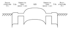
酸化物半導体層205に接する導電膜は酸素親和性の高い金属を含む材料が好ましい。
The conductive film in contact with the
酸素親和性の高い金属としては、チタン(Ti)、アルミニウム(Al)、マンガン(M
n)、マグネシウム(Mg)、ジルコニウム、ベリリウム、トリウムのいずれか一または
複数から選択された材料であることが好ましい。本実施の形態ではチタン膜を用いる。
Metals with high oxygen affinity include titanium (Ti), aluminum (Al), and manganese (M
It is preferable that the material be one or more selected from the group consisting of arsenic (arsenic), magnesium (Mg), zirconium, beryllium, and thorium. In this embodiment, a titanium film is used.
酸化物半導体層と酸素親和性の高い導電膜を接して形成すると、界面付近のキャリア密度
が増加し、低抵抗な領域が形成され、酸化物半導体と、導電膜のコンタクト抵抗を低減で
きる。これは、酸素親和性の高い導電膜が酸化物半導体層から酸素を引き抜くことにより
、酸化物半導体層と導電膜の界面に、酸化物半導体層中の金属が過剰な層(複合層とも呼
ぶ。)または酸化された導電膜のいずれか、もしくはその両方が形成されることによる。
例えば、In-Ga-Zn-O系の酸化物半導体層とチタン膜が接する構成においては、
酸化物半導体層とチタン膜に接する界面付近に、インジウムが過剰な層と酸化チタン層が
生成する場合がある。また、酸化物半導体層とチタン膜に接する界面付近に、インジウム
が過剰な層または酸化チタン層のいずれかが生成する場合がある。In-Ga-Zn-O
系の酸化物半導体層から酸素が欠損したインジウムが過剰な層は電気伝導度が高く、酸化
物半導体層と導電膜との接触抵抗の低減を図ることができる。
When an oxide semiconductor layer is formed in contact with a conductive film having high oxygen affinity, the carrier density near the interface is increased, a low-resistance region is formed, and the contact resistance between the oxide semiconductor and the conductive film can be reduced. This is because the conductive film having high oxygen affinity extracts oxygen from the oxide semiconductor layer, so that either a layer containing excess metal in the oxide semiconductor layer (also referred to as a composite layer) or an oxidized conductive film, or both, are formed at the interface between the oxide semiconductor layer and the conductive film.
For example, in a structure in which an In—Ga—Zn—O-based oxide semiconductor layer is in contact with a titanium film,
A layer containing excessive indium and a titanium oxide layer may be formed near the interface between the oxide semiconductor layer and the titanium film. In addition, either a layer containing excessive indium or a titanium oxide layer may be formed near the interface between the oxide semiconductor layer and the titanium film.
A layer in which oxygen is lost from the oxide semiconductor layer and indium is excessive has high electrical conductivity, and contact resistance between the oxide semiconductor layer and a conductive film can be reduced.
なお、酸化物半導体層と接する導電膜として導電性を有する酸化チタン膜を用いても良い
。その場合、In-Ga-Zn-O系の酸化物半導体層と酸化チタン膜が接する構成にお
いては、酸化物半導体層と酸化チタン膜に接する界面付近に、インジウムが過剰な層が生
成する場合がある。
Note that a conductive titanium oxide film may be used as a conductive film in contact with the oxide semiconductor layer. In that case, in a structure in which an In—Ga—Zn—O-based oxide semiconductor layer is in contact with a titanium oxide film, a layer containing excess indium may be generated near the interface between the oxide semiconductor layer and the titanium oxide film.
なお以上の、In-Ga-Zn-O系酸化物半導体膜を薄膜トランジスタの活性層として
用いたチャネルエッチ構造の薄膜トランジスタにおいて、ソース電極またはドレイン電極
として用いる金属膜と、In-Ga-Zn-O系酸化物半導体膜との界面近傍において、
インジウムの濃度が他の領域よりも高い層(Inリッチな層)と、酸化チタン膜(TiO
X)が形成される現象については、実施の形態14で詳しく説明する。
In addition, in the above-mentioned thin film transistor having a channel etch structure in which the In—Ga—Zn—O-based oxide semiconductor film is used as an active layer of the thin film transistor, in the vicinity of the interface between the metal film used as the source electrode or the drain electrode and the In—Ga—Zn—O-based oxide semiconductor film,
A layer having a higher indium concentration than other regions (In-rich layer) and a titanium oxide film (TiO
The phenomenon in which X 2 is formed will be described in detail in the fourteenth embodiment.
導電膜は100nm以上500nm以下、好ましくは200nm以上300nm以下の厚
さで形成する。なお、導電膜の成膜方法は、スパッタ法や真空蒸着法(電子ビーム蒸着法
など)や、アーク放電イオンプレーティング法や、スプレー法を用いる。また、銀、金、
銅などの導電性ナノペーストを用いてスクリーン印刷法、インクジェット法などを用いて
吐出し焼成して形成しても良い。
The conductive film is formed to a thickness of 100 nm to 500 nm, preferably 200 nm to 300 nm. The conductive film is formed by sputtering, vacuum deposition (electron beam deposition, etc.), arc discharge ion plating, or spraying.
The
次いで、該導電膜上にフォトリソグラフィ法またはインクジェット法等によりマスクを形
成し、該マスクを用いて導電膜をエッチングして、ソース電極として機能する電極207
a、ドレイン電極として機能する電極207bを形成することができる。本実施の形態で
は、導電膜としてスパッタリング法で厚さ200nmのTiを形成し、第5のフォトリソ
グラフィ工程で形成したレジストマスクを用いて、ドライエッチング法にて導電膜を選択
的にエッチングして、電極207a、電極207bを形成する。
Next, a mask is formed on the conductive film by a photolithography method, an ink-jet method, or the like, and the conductive film is etched using the mask to form an
In this embodiment mode, a Ti film having a thickness of 200 nm is formed as a conductive film by a sputtering method, and the conductive film is selectively etched by a dry etching method using a resist mask formed in a fifth photolithography process, to form the
また、第5のフォトリソグラフィ工程においては、酸化物半導体層上に接する導電膜のみ
を選択的に除去する部分がある。酸化物半導体層上に接する導電膜のみを選択的に除去す
るため、アルカリ性のエッチャントとしてアンモニア過水(組成の重量比として、過酸化
水素:アンモニア:水=5:2:2)などを用いると、金属導電膜を選択的に除去し、I
n-Ga-Zn-O系酸化物半導体からなる酸化物半導体層を残存させることができる。
In the fifth photolithography step, only the conductive film in contact with the oxide semiconductor layer is selectively removed. In order to selectively remove only the conductive film in contact with the oxide semiconductor layer, an alkaline etchant such as ammonia hydrogen peroxide (w/w ratio of hydrogen peroxide:ammonia:water=5:2:2) is used to selectively remove the metal conductive film, and the I
An oxide semiconductor layer made of an n-Ga-Zn-O based oxide semiconductor can be left.
また、エッチング条件にもよるが第5のフォトリソグラフィ工程において酸化物半導体層
の露出領域がエッチングされる場合がある。その場合、ソース電極層とドレイン電極層に
挟まれる領域(207aと207bに挟まれる領域)の酸化物半導体層の厚みは、ゲート
配線203上でソース電極層が重なる領域の酸化物半導体層の厚み、又はドレイン電極層
が重なる領域の酸化物半導体層の厚みに比べ、薄くなる。(図4(D)参照)。
Depending on the etching conditions, an exposed region of the oxide semiconductor layer may be etched in the fifth photolithography step. In that case, the thickness of the oxide semiconductor layer in a region sandwiched between the source electrode layer and the drain electrode layer (a region sandwiched between 207a and 207b) is thinner than the thickness of the oxide semiconductor layer in a region overlapping with the source electrode layer over the
次いで、絶縁層208をゲート絶縁層204、酸化物半導体層205上に形成する。絶縁
層208は水分や、水素イオンや、OH-などの不純物を含まず、これらが外部から侵入
することを防ぐ無機絶縁膜を用いて形成する。また、絶縁層208は後の工程で形成する
ソース配線から、Cuを含む層のマイグレーションを抑制する無機絶縁膜を用いて形成す
る。本実施の形態では、絶縁層208a上に絶縁層208bを積層して絶縁層208を形
成する。
Next, an insulating
酸化物半導体層205と接する絶縁層208aには、酸化物絶縁膜を用いる。絶縁層20
8aは、少なくとも1nm以上の膜厚とし、スパッタリング法など、酸化物絶縁膜に水、
水素等の不純物を混入させない方法を適宜用いて形成することができる。代表的には酸化
珪素膜、窒化酸化珪素膜、酸化アルミニウム膜、または酸化窒化アルミニウム膜などを用
い、単層または積層して形成する。
An oxide insulating film is used for the insulating
The insulating film 8a has a thickness of at least 1 nm.
The insulating film can be formed by appropriately using a method that does not mix impurities such as hydrogen, etc. Typically, the insulating film is formed by using a silicon oxide film, a silicon nitride oxide film, an aluminum oxide film, an aluminum oxynitride film, or the like, in a single layer or a stacked layer.
成膜時の基板温度は、室温以上300℃以下とすればよく、本実施の形態では100℃と
する。酸化珪素膜のスパッタリング法による成膜は、希ガス(代表的にはアルゴン)雰囲
気下、酸素雰囲気下、または希ガス(代表的にはアルゴン)及び酸素雰囲気下において行
うことができる。なお、スパッタ法で形成した酸化物絶縁膜は特に緻密であり、接する層
へ不純物が拡散する現象を抑制する保護膜として単層であっても利用することができる。
また、リン(P)や硼素(B)をドープしたターゲットを用い、酸化物絶縁膜にリン(P
)や硼素(B)を添加することもできる。
The substrate temperature during film formation may be from room temperature to 300° C. inclusive, and is set to 100° C. in this embodiment. The silicon oxide film can be formed by sputtering in a rare gas (typically argon) atmosphere, an oxygen atmosphere, or a rare gas (typically argon) and oxygen atmosphere. Note that an oxide insulating film formed by sputtering is particularly dense and can be used as a single layer as a protective film that suppresses the phenomenon of impurities diffusing into a layer in contact with it.
In addition, a phosphorus (P) or boron (B) doped target is used to deposit phosphorus (P) on the oxide insulating film.
) and boron (B) can also be added.
また、ターゲットとして酸化珪素ターゲットまたは珪素ターゲットを用いることができ、
特に珪素ターゲットが好ましい。珪素ターゲットを用いて、酸素、及び希ガス雰囲気下で
スパッタリング法により成膜した酸化珪素膜は、珪素原子または酸素原子の未結合手(ダ
ングリングボンド)を多く含んでいる。
In addition, a silicon oxide target or a silicon target can be used as the target.
A silicon target is particularly preferable. A silicon oxide film formed by sputtering a silicon target in an atmosphere of oxygen and rare gas contains many dangling bonds of silicon atoms or oxygen atoms.
絶縁層208aは未結合手を多く含むため、酸化物半導体層205に含まれる不純物は、
酸化物半導体層205と絶縁層208aが接する界面を介して、絶縁層208aに拡散し
易くなる。具体的には、酸化物半導体層205に含まれる水素原子や、H2Oなど水素原
子を含む化合物や、炭素原子を含む化合物等が絶縁層208aに拡散移動し易くなり、絶
縁層208aに固定化される。
Since the insulating
The hydrogen atoms contained in the
本実施の形態では、純度が6Nであり、柱状多結晶Bドープの珪素ターゲット(抵抗値0
.01Ωcm)を用い、基板とターゲットの間との距離(T-S間距離)を89mm、圧
力0.4Pa、直流(DC)電源6kW、酸素(酸素流量比率100%)雰囲気下でパル
スDCスパッタ法により成膜する。膜厚は300nmとする。
In this embodiment, a columnar polycrystalline B-doped silicon target (resistance value 0.01 mm) with a purity of 6N is used.
The film is formed by pulse DC sputtering using a target having a resistivity of 0.01 Ωcm, a distance between the substrate and the target (T-S distance) of 89 mm, a pressure of 0.4 Pa, a direct current (DC) power supply of 6 kW, and an oxygen (oxygen flow rate ratio of 100%) atmosphere. The film thickness is 300 nm.
この段階で、酸化物半導体層205と酸化物絶縁層208aが接する領域が形成される。
ゲート電極に重畳し、ゲート絶縁層204と絶縁層208aに接して挟まれる酸化物半導
体層205の領域がチャネル形成領域となる。また、絶縁層208aはチャネル保護層と
して機能する。
At this stage, a region where the
A region of the
絶縁層208a上に形成する絶縁層208bには、窒素を含む絶縁膜を用いる。絶縁層2
08bは、少なくとも1nm以上の膜厚とし、スパッタリング法など、絶縁膜に水、水素
等の不純物を混入させない方法を適宜用いて形成する。代表的には窒化珪素膜、窒化酸化
珪素膜、または窒化アルミニウム膜などを用いる。本実施の形態では、RFスパッタ法を
用いて窒化珪素膜の絶縁層208bを形成する。
The insulating
The insulating
本実施の形態では、絶縁層208bとして厚さ400nmの窒化珪素膜を形成する。
In this embodiment, a silicon nitride film with a thickness of 400 nm is formed as the insulating
次いで、電極207aとソース配線209を接続するための開口部216(コンタクトホ
ールともいう)を絶縁層208に形成する。絶縁層208上にフォトリソグラフィ法また
はインクジェット法等によりマスクを形成し、該マスクを用いて絶縁層208を選択的に
エッチングしてコンタクトホールを形成する。本実施の形態では、第6のフォトリソグラ
フィ工程で形成したレジストマスクを用いて絶縁層208を選択的にエッチングして、コ
ンタクトホールを形成する。
Next, an opening 216 (also referred to as a contact hole) for connecting the
次いで、ソース配線209を形成するため、スパッタリング法、真空蒸着法などを用いて
W、Ta、Mo、Ti、CrなどのCuよりも融点が高い導電膜、または上述した元素を
組み合わせた合金等を導電膜として5nm以上200nm以下、好ましくは10nm以上
100nm以下の厚さで形成する。また、反応性スパッタリング法にて窒化タンタル(T
aN)、窒化チタン(TiN)を形成してもよい。
Next, in order to form the
Alternatively, titanium nitride (TiN) or titanium nitride (TiN) may be formed.
続いて、スパッタリング法、真空蒸着法、またはメッキ法を用いてCuを含む導電膜を1
00nm以上500nm以下、好ましくは200nm以上300nm以下の厚さで形成し
、該導電膜上にフォトリソグラフィ法またはインクジェット法等によりマスクを形成し、
該マスクを用いてCuを含む導電膜及びソース配線209を形成するための導電膜をエッ
チングしてソース配線209及びソース配線210を形成することができる。
Next, a conductive film containing Cu is formed on the substrate by sputtering, vacuum deposition, or plating.
a mask is formed on the conductive film by a photolithography method, an ink-jet method, or the like;
The conductive film containing Cu and the conductive film for forming the
本実施の形態では、ソース配線209を形成するための導電膜に厚さ50nmの窒化チタ
ン膜を用い、ソース配線210を形成するための導電膜に厚さ250nmのCu膜を用い
、第7のフォトリソグラフィ工程で形成したレジストマスクを用いて導電膜を選択的にエ
ッチングして、ソース配線209及びソース配線210を形成する(図5(A)参照)。
In this embodiment, a 50-nm-thick titanium nitride film is used as a conductive film for forming the
ソース配線を、Cuを含む層と、Cuよりも融点が高い元素を含む層の積層とすることで
、Cuを含む層のマイグレーションを抑制し、半導体装置の信頼性を向上させることがで
きる。さらに、ソース配線210の上にもCuよりも融点が高い元素を含む層を設け、C
uを含む層をCuよりも融点が高い元素を含む層で挟む構造としてもよい。なお、半導体
装置の使用環境や使用条件によっては、Cuを含む層のみでソース配線を形成してもよい
。
By forming the source wiring as a laminate of a layer containing Cu and a layer containing an element having a melting point higher than that of Cu, migration in the layer containing Cu can be suppressed, and the reliability of the semiconductor device can be improved.
A structure in which a layer containing u is sandwiched between layers containing an element having a melting point higher than that of Cu may be used. Depending on the environment and conditions in which the semiconductor device is used, the source wiring may be formed only of a layer containing Cu.
次いで、絶縁層211を50nm以上300nm以下、好ましくは100nm以上200
nm以下の厚さで形成する。絶縁層211は、絶縁層201と同様の方法で形成すること
ができる。本実施の形態では、絶縁層211として厚さ10nmの窒化珪素膜を形成する
。また、絶縁層211は保護層としても機能する。Cuを含む導電層の下側及び上側に位
置する絶縁層を、窒化珪素を含む絶縁層とし、該絶縁層でCuを含む導電層を挟む、もし
くは包むことで、Cu拡散を防ぐことができる(図5(B)参照)。
Next, the insulating
The insulating
次いで、電極207bと画素電極として機能する電極212を接続するためのコンタクト
ホールを絶縁層211及び絶縁層208に形成する。絶縁層211上にフォトリソグラフ
ィ法またはインクジェット法等によりマスクを形成し、該マスクを用いて絶縁層211及
び絶縁層208を選択的にエッチングしてコンタクトホールを形成する。本実施の形態で
は、第8のフォトリソグラフィ工程で形成したレジストマスクを用いて絶縁層211及び
絶縁層208を選択的にエッチングして、コンタクトホール(開口部217)を形成する
。
Next, a contact hole for connecting the
次いで、スパッタリング法、真空蒸着法などを用いて、透光性を有する導電膜を30nm
以上200nm以下、好ましくは50nm以上100nm以下の厚さで形成し、該導電膜
上にフォトリソグラフィ法またはインクジェット法等によりマスクを形成し、該マスクを
用いて該導電膜をエッチングして画素電極として機能する電極212を形成することがで
きる。
Next, a light-transmitting conductive film is formed to a thickness of 30 nm by using a sputtering method, a vacuum deposition method, or the like.
The conductive film is formed to a thickness of 200 nm or more, preferably 50 nm or more and 100 nm or less, and a mask is formed on the conductive film by photolithography, inkjet, or the like. The conductive film is etched using the mask to form the
透光性を有する導電膜としては、酸化タングステンを含むインジウム酸化物、酸化タング
ステンを含むインジウム亜鉛酸化物、酸化チタンを含むインジウム酸化物、酸化チタンを
含むインジウム錫酸化物、インジウム錫酸化物(以下、ITOと示す。)、インジウム亜
鉛酸化物、酸化ケイ素を添加したインジウム錫酸化物などの透光性を有する導電性材料を
用いることができる。
As the light-transmitting conductive film, a light-transmitting conductive material such as indium oxide containing tungsten oxide, indium zinc oxide containing tungsten oxide, indium oxide containing titanium oxide, indium tin oxide containing titanium oxide, indium tin oxide (hereinafter referred to as ITO), indium zinc oxide, or indium tin oxide to which silicon oxide has been added can be used.
また、透光性を有する導電膜を、導電性高分子(導電性ポリマーともいう)を含む導電性
組成物を用いて形成することができる。導電性組成物を用いて形成した画素電極は、シー
ト抵抗が10000Ω/□以下、波長550nmにおける透光率が70%以上であること
が好ましい。また、導電性組成物に含まれる導電性高分子の抵抗率が0.1Ω・cm以下
であることが好ましい。
A light-transmitting conductive film can be formed using a conductive composition containing a conductive polymer. A pixel electrode formed using the conductive composition preferably has a sheet resistance of 10,000 Ω/□ or less and a light transmittance of 70% or more at a wavelength of 550 nm. The resistivity of the conductive polymer contained in the conductive composition is preferably 0.1 Ω cm or less.
本実施の形態では、透光性を有する導電膜として厚さ80nmのITOを形成し、第9の
フォトリソグラフィ工程で形成したレジストマスクを用いて透光性を有する導電膜を選択
的にエッチングして、画素電極として機能する電極212を形成する(図5(C)参照)
。
In this embodiment mode, ITO having a thickness of 80 nm is formed as a light-transmitting conductive film, and the light-transmitting conductive film is selectively etched using a resist mask formed in a ninth photolithography process to form an
.
なお、本実施の形態ではゲート絶縁層204と、酸化物半導体層205を連続成膜するが
、成膜したゲート絶縁層204を大気に暴露し、その後酸化物半導体層205を形成して
もよい。その場合は、ゲート絶縁層204を不活性ガス雰囲気(窒素、またはヘリウム、
ネオン、アルゴン等)下において加熱処理(400℃以上であって基板の歪み点未満)す
ることが好ましい。この加熱処理により、酸化物半導体膜の成膜前にゲート絶縁層204
内に含まれる水素及び水などの不純物を除去することができる。
Note that in this embodiment, the
It is preferable that the
Impurities such as hydrogen and water contained in the fuel can be removed.
また、酸化珪素層、窒化珪素層、酸化窒化珪素層又は窒化酸化珪素層は、スパッタリング
法の他プラズマCVD法を用いて形成してもよい。例えば、成膜ガスとして、SiH4、
酸素及び窒素を用いてプラズマCVD法により酸化窒化珪素層を形成すればよい。ゲート
絶縁層204の膜厚は、100nm以上500nm以下とし、積層の場合は、例えば、厚
50nm以上200nm以下の第1のゲート絶縁層と、第1のゲート絶縁層上に膜厚5n
m以上300nm以下の第2のゲート絶縁層の積層とする。なお、プラズマCVD法等を
用いて形成した膜が水素及び水などの不純物を含む場合、上記の加熱処理を施し、不純物
を除去した後に酸化物半導体膜を成膜するのが好ましい。
The silicon oxide layer, the silicon nitride layer, the silicon oxynitride layer, or the silicon nitride oxide layer may be formed by a plasma CVD method other than a sputtering method.
A silicon oxynitride layer may be formed by plasma CVD using oxygen and nitrogen. The thickness of the
In the case where a film formed by a plasma CVD method or the like contains impurities such as hydrogen and water, the impurities are preferably removed by the above-described heat treatment before the oxide semiconductor film is formed.
なお、本実施の形態では、第4のフォトリソグラフィ工程によりゲート絶縁層を選択的に
エッチングして図示されていないゲート配線層に達するコンタクトホールを形成するが、
この方法に限定されない。例えば、ゲート絶縁層204を形成した後、ゲート絶縁層上に
レジストマスクを形成し、ゲート配線層に達するコンタクトホールを形成してもよい。
In this embodiment, the gate insulating layer is selectively etched by the fourth photolithography process to form a contact hole reaching a gate wiring layer (not shown).
This method is not limited to the above, but may be modified in such a way that, after the
また、酸化物半導体層205を形成した後、酸化物半導体層205の脱水化または脱水素
化を行ってもよい。
After the
脱水化または脱水素化を行う第1の加熱処理の温度は、400℃以上であって750℃未
満、好ましくは425℃以上とする。なお、425℃以上であれば熱処理時間は1時間以
下でよいが、425℃未満であれば加熱処理時間は、1時間よりも長時間行うこととする
。第1の加熱処理では、加熱処理装置の一つである電気炉に基板を導入し、酸化物半導体
層に対して窒素雰囲気下において加熱処理を行った後、大気に触れることなく、酸化物半
導体層への水や水素の再混入を防ぎ、酸化物半導体層を得る。酸化物半導体層の脱水化ま
たは脱水素化を行う加熱温度Tから、再び水が入らないような十分な温度まで同じ炉を用
い、具体的には加熱温度Tよりも100℃以上下がるまで窒素雰囲気下で徐冷する。また
、窒素雰囲気に限定されず、ヘリウム、ネオン、アルゴン等の希ガス雰囲気下において脱
水化または脱水素化を行う。
The temperature of the first heat treatment for dehydration or dehydrogenation is 400° C. or higher and lower than 750° C., preferably 425° C. or higher. If the temperature is 425° C. or higher, the heat treatment time may be 1 hour or shorter, whereas if the temperature is lower than 425° C., the heat treatment time is longer than 1 hour. In the first heat treatment, the substrate is introduced into an electric furnace, which is one of heat treatment apparatuses, and the oxide semiconductor layer is subjected to heat treatment in a nitrogen atmosphere. Then, the oxide semiconductor layer is obtained without being exposed to air and preventing re-mixing of water or hydrogen into the oxide semiconductor layer. The oxide semiconductor layer is gradually cooled in a nitrogen atmosphere from a heating temperature T for dehydrating or dehydrogenating the oxide semiconductor layer to a temperature sufficient to prevent re-mixing of water, specifically, until the temperature is 100° C. or higher lower than the heating temperature T. The dehydration or dehydrogenation is performed in a rare gas atmosphere such as helium, neon, or argon, without being limited to a nitrogen atmosphere.
なお、加熱処理装置は電気炉に限られず、例えば、GRTA(Gas Rapid Th
ermal Anneal)装置、LRTA(Lamp Rapid Thermal
Anneal)装置等のRTA(Rapid Thermal Anneal)装置を用
いることができる。LRTA装置は、ハロゲンランプ、メタルハライドランプ、キセノン
アークランプ、カーボンアークランプ、高圧ナトリウムランプ、高圧水銀ランプなどのラ
ンプから発する光(電磁波)の輻射により、被処理物を加熱する装置である。GRTA装
置は、上記のランプから発する光による熱輻射、およびランプから発する光で気体を加熱
し、加熱された気体からの熱伝導によって、被処理物を加熱する装置である。気体には、
アルゴンなどの希ガス、または窒素のような、加熱処理によって被処理物と反応しない不
活性気体が用いられる。また、LRTA装置、GRTA装置には、ランプだけでなく、抵
抗発熱体などの発熱体からの熱伝導または熱輻射によって、被処理物を加熱する装置を備
えていてもよい。
The heat treatment device is not limited to an electric furnace, and may be, for example, a GRTA (Gas Rapid Transient Annealing) device.
thermal annealing) device, LRTA (Lamp Rapid Thermal)
For example, an RTA (Rapid Thermal Anneal) apparatus such as a LRTA apparatus can be used. The LRTA apparatus is an apparatus that heats the workpiece by radiation of light (electromagnetic waves) emitted from a lamp such as a halogen lamp, a metal halide lamp, a xenon arc lamp, a carbon arc lamp, a high-pressure sodium lamp, or a high-pressure mercury lamp. The GRTA apparatus is an apparatus that heats the workpiece by thermal radiation from the light emitted from the lamps, and by heating a gas with the light emitted from the lamp, and by thermal conduction from the heated gas. The gas may be, for example,
An inert gas that does not react with the workpiece by heat treatment, such as a rare gas such as argon or nitrogen, is used. The LRTA apparatus and the GRTA apparatus may also be equipped with a device that heats the workpiece by heat conduction or heat radiation from a heating element such as a resistance heating element, in addition to the lamp.
また、第1の加熱処理においては、窒素、またはヘリウム、ネオン、アルゴン等の希ガス
に、水、水素などが含まれないことが好ましい。または、加熱処理装置に導入する窒素、
またはヘリウム、ネオン、アルゴン等の希ガスの純度を、6N(99.9999%)以上
、好ましくは7N(99.99999%)以上、(即ち不純物濃度を1ppm以下、好ま
しくは0.1ppm以下)とすることが好ましい。
In the first heat treatment, it is preferable that nitrogen or a rare gas such as helium, neon, or argon does not contain water, hydrogen, or the like.
Alternatively, it is preferable that the purity of rare gas such as helium, neon, or argon is 6N (99.9999%) or more, preferably 7N (99.99999%) or more (i.e., impurity concentration is 1 ppm or less, preferably 0.1 ppm or less).
なお、第1の加熱処理の条件、または酸化物半導体層の材料によっては、酸化物半導体層
が結晶化し、微結晶膜または多結晶膜となる場合もある。例えば、結晶化率が90%以上
、または80%以上の微結晶の酸化物半導体層となる場合もある。また、第1の加熱処理
の条件、または酸化物半導体層の材料によっては、結晶成分を含まない非晶質の酸化物半
導体膜となる場合もある。
Depending on the conditions of the first heat treatment or the material of the oxide semiconductor layer, the oxide semiconductor layer may be crystallized to become a microcrystalline film or a polycrystalline film. For example, the oxide semiconductor layer may be a microcrystalline film with a crystallization rate of 90% or more, or 80% or more. Depending on the conditions of the first heat treatment or the material of the oxide semiconductor layer, the oxide semiconductor layer may be an amorphous oxide semiconductor film that does not contain a crystalline component.
酸化物半導体層は、第1の加熱処理後に酸素欠乏型となり、低抵抗化する。第1の加熱処
理後の酸化物半導体膜は、成膜直後の酸化物半導体膜よりもキャリア濃度が高まり、好ま
しくは1×10¹⁸/cm3以上のキャリア濃度を有する酸化物半導体層となる。
The oxide semiconductor layer becomes oxygen-deficient and has low resistance after the first heat treatment. The oxide semiconductor film after the first heat treatment has a higher carrier concentration than the oxide semiconductor film immediately after deposition, and preferably has a carrier concentration of 1×10 18 /cm 3 or more.
また、酸化物半導体層の第1の加熱処理は、島状の酸化物半導体層に加工する前の酸化物
半導体膜に行うこともできる。その場合には、第1の加熱処理後に、加熱装置から基板を
取り出し、第3のフォトリソグラフィ工程を行う。
The first heat treatment of the oxide semiconductor layer can be performed on the oxide semiconductor film before it is processed into an island-shaped oxide semiconductor layer. In that case, after the first heat treatment, the substrate is taken out of the heating apparatus and a third photolithography step is performed.
また、絶縁層208の形成後、第2の加熱処理(好ましくは200℃以上400℃以下、
例えば250℃以上350℃以下)を不活性ガス雰囲気下、または窒素ガス雰囲気下で行
ってもよい。
After the insulating
For example, the heating at a temperature of 250° C. or higher and 350° C. or lower may be performed in an inert gas atmosphere or a nitrogen gas atmosphere.
例えば、窒素雰囲気下で250℃、1時間の第2の加熱処理を行う。第2の加熱処理を行
うと、酸化物半導体層205の一部が酸化物絶縁層208aと接した状態で加熱され、ま
た、酸化物半導体層205の他の一部が電極207a、電極207bと接した状態で加熱
される。
For example, the second heat treatment is performed in a nitrogen atmosphere at 250° C. for 1 hour. By the second heat treatment, part of the
第1の加熱処理で低抵抗化された酸化物半導体層205が酸化物絶縁層208aと接した
状態で第2の加熱処理が施されると、酸化物絶縁層208aが接した領域が酸素過剰な状
態となる。その結果、酸化物半導体層205の酸化物絶縁層208aが接する領域から、
酸化物半導体層205の深さ方向に向けて、高抵抗化(I型化)する。
When the second heat treatment is performed in a state in which the
The
具体的には、酸化物半導体層205と酸化物絶縁層208aが接する界面からゲート絶縁
層204にかけて、高抵抗化(I型化)された領域を有する酸化物半導体層205が形成
される。
Specifically, the
本実施の形態で作製された薄膜トランジスタはチャネル形成領域に高抵抗化(I型化)さ
れた酸化物半導体層が形成されているため、閾値電圧が正の値を示し、エンハンスメント
型の挙動を示す。
Since a high-resistance (i-type) oxide semiconductor layer is formed in a channel formation region of the thin film transistor manufactured in this embodiment, the threshold voltage has a positive value and exhibits enhancement-type behavior.
なお、酸素との親和性が強い金属導電膜からなる電極207a、電極207bと酸化物半
導体層205が接する領域に第2の加熱処理を行うと、該金属導電膜側に酸素が移動しや
すくなり、酸素との親和性が強い金属導電膜と接する領域の該酸化物半導体層はN型化す
る。酸素と親和性が強い金属としては、例えばTiをその例に挙げることができる。
When the second heat treatment is performed on the region where the
また、第2の加熱処理を行うタイミングは、第6のフォトリソグラフィ工程の終了直後に
限定されず、第6のフォトリソグラフィ工程よりも後の工程であれば特に限定されない。
Furthermore, the timing of performing the second heat treatment is not limited to immediately after the end of the sixth photolithography process, and is not particularly limited as long as it is a process subsequent to the sixth photolithography process.
なお、本実施の形態において、多階調マスクを用いたフォトリソグラフィ工程を適用する
こともできる。多階調マスクを用いたフォトリソグラフィ工程について、図6及び図7を
用いて説明する。
In this embodiment, a photolithography process using a multi-tone mask can also be applied. The photolithography process using a multi-tone mask will be described with reference to FIGS.
多階調マスクとは、多段階の光量で露光を行うことが可能なマスクであり、代表的には露
光部分、中間露光部分、及び未露光部分に3つの露光レベルで露光を行う。一度の露光及
び現像工程により、複数(代表的には二種類)の厚さの領域を有するレジストマスクを形
成することが可能である。このため、多階調マスクを用いることで、露光マスクの枚数を
削減することが可能である。
A multi-tone mask is a mask capable of performing exposure with multiple levels of light intensity, typically performing exposure with three exposure levels for exposed, intermediately exposed, and unexposed parts. A resist mask having regions with multiple (typically two types) thicknesses can be formed by a single exposure and development process. Therefore, by using a multi-tone mask, it is possible to reduce the number of exposure masks.
多階調マスクの代表例としては、図6(A)に示すようなグレートーンマスク801a、
図6(C)に示すようなハーフトーンマスク801bがある。
A typical example of a multi-tone mask is a gray-
There is a half-
図6(A)に示すように、グレートーンマスク801aは、透光性基板802及びその上
に形成される遮光部803並びに回折格子804で構成される。遮光部803においては
、光の透過率が0%である。一方、回折格子804はスリット、ドット、メッシュ等の光
透過部の間隔を、露光に用いる光の解像度限界以下の間隔とすることにより、光の透過率
を制御することができる。なお、回折格子804は、周期的なスリット、ドット、メッシ
ュ、または非周期的なスリット、ドット、メッシュどちらも用いることができる。
As shown in Fig. 6A, the
透光性基板802としては、石英等の透光性基板を用いることができる。遮光部803及
び回折格子804は、クロムや酸化クロム等の光を吸収する遮光材料を用いて形成するこ
とができる。
A light-transmitting substrate such as quartz can be used as the light-transmitting
グレートーンマスク801aに露光光を照射した場合、図6(B)に示すように、遮光部
803においては、光透過率805は0%であり、遮光部803及び回折格子804が設
けられていない領域では光透過率805は100%である。また、回折格子804が設け
られた領域における光透過率805は、10~70%の範囲で調整可能である。回折格子
804における光の透過率の調整は、回折格子のスリット、ドット、またはメッシュの間
隔及びピッチの調整により可能である。
6B, when the
図6(C)に示すように、ハーフトーンマスク801bは、透光性基板802及びその上
に形成される半透過部807並びに遮光部806で構成される。半透過部807は、Mo
SiN、MoSi、MoSiO、MoSiON、CrSiなどを用いることができる。遮
光部806は、クロムや酸化クロム等の光を吸収する遮光材料を用いて形成することがで
きる。
As shown in FIG. 6C, the half-
Examples of materials that can be used include SiN, MoSi, MoSiO, MoSiON, and CrSi. The
ハーフトーンマスク801bに露光光を照射した場合、図6(D)に示すように、遮光部
806においては、光透過率808は0%であり、遮光部806及び半透過部807が設
けられていない領域では光透過率808は100%である。また、半透過部807が設け
られた領域における光透過率808は、10~70%の範囲で調整可能である。半透過部
807における光の透過率の調整は、半透過部807の材料により調整により可能である
。
6D, when the
続いて、図7を用いて、前述した第3のフォトリソグラフィ工程と第5のフォトリソグラ
フィ工程を、1回の多階調マスクを用いたフォトリソグラフィ工程に置き換える例につい
て説明する。
Next, an example in which the above-described third and fifth photolithography steps are replaced with a single photolithography step using a multi-tone mask will be described with reference to FIG.
前述した本実施の形態の第3のフォトリソグラフィ工程では、絶縁層204上に半導体層
205を形成した後に島状の半導体層としていたが、ここでは島状の半導体層とせず、続
けて半導体層205上に電極層207を形成する。次いで、電極層207の上に多階調マ
スクを用いて、凹部又は凸部を有するレジストマスク231を形成する(図7(A)参照
)。
In the third photolithography step of the present embodiment described above, the
レジストマスク231は、厚さの異なる複数の領域(ここでは、2つの領域)からなるレ
ジストマスクともいうことができる。レジストマスク231において、厚い領域をレジス
トマスク231の凸部と呼び、薄い領域をレジストマスク231の凹部と呼ぶこととする
。
The resist
レジストマスク231において、ソース電極として機能する電極207a及びドレイン電
極として機能する電極207bが形成される部分には凸部が形成され、電極207a及び
電極207bが形成される部分に挟まれている部分には凹部が形成される。
In the resist
次いで、レジストマスク231を用いて、電極層207、及び半導体層205を選択的か
つ同時にエッチングし、島状の半導体層205を形成する(図7(B)参照)。
Next, the
次いで、レジストマスク231を後退(縮小)させることで、レジストマスク231a、
レジストマスク231bを形成する。レジストマスクを後退(縮小)させるには、酸素プ
ラズマによるアッシング等を行えばよい。レジストマスクを後退(縮小)させることによ
り、レジストマスク231aとレジストマスク231bに挟まれた部分の電極層207が
露出する(図7(C)参照)。
Next, the resist
A resist
次いで、レジストマスク231a及びレジストマスク231bに挟まれた部分の電極層2
07を、レジストマスク231a及びレジストマスク231bを用いて選択的にエッチン
グすることにより、電極207a、及び電極207bを形成する。なお、この時、半導体
層205は一部のみがエッチングされ、溝部(凹部)を有する半導体層となる。また、半
導体層205の端部が、電極207a及び電極207bの端部より外側に突出した形状と
なる。(図7(D)参照)。次いで、レジストマスク231a及びレジストマスク231
bを除去する(図7(E)参照)。
Next, the
7D , the
b is removed (see FIG. 7(E)).
多階調マスクを用いると、複数回のフォトリソグラフィ工程を一回のフォトリソグラフィ
工程に置き換えることが可能となるため、半導体装置の生産性を向上させることができる
。
By using a multi-tone mask, it becomes possible to replace a plurality of photolithography steps with a single photolithography step, thereby improving the productivity of semiconductor devices.
なお、本実施の形態において、第6のフォトリソグラフィ工程において電極207aとソ
ース配線209を接続するためのコンタクトホールを形成する際に、薄膜トランジスタを
囲むように、絶縁層204b、絶縁層208a及び絶縁層208bに開口を形成し、絶縁
層211が該開口を介して絶縁層204aと接するような構造の薄膜トランジスタ253
を形成してもよい。薄膜トランジスタ253の断面図を図38に例示する。
In this embodiment mode, when a contact hole for connecting the
A cross-sectional view of the
図38に例示した薄膜トランジスタ253は、薄膜トランジスタ250と同様に、チャネ
ルエッチ型の薄膜トランジスタであり、基板200上に設けられた絶縁層201と、絶縁
層201に設けられたゲート配線202と、ゲート配線202上に設けられたゲート配線
203と、ゲート配線203上に設けられた絶縁層204aと、絶縁層204a上に設け
られた絶縁層204bと、絶縁層204b上に設けられた半導体層205と、半導体層2
05上に設けられた一対の電極207a及び電極207bと、電極207a、電極207
b、及び半導体層205上に設けられた絶縁層208aと、絶縁層208a上に設けられ
た絶縁層208bと、絶縁層208a及び絶縁層208bに設けられた開口部を介して電
極207aに接するソース配線209と、ソース配線209上に設けられたソース配線2
10と、ソース配線210上に設けられた絶縁層211と、絶縁層211、絶縁層208
a及び絶縁層208bに設けられた開口部を介して電極207bに接する電極212と、
を有する。
The
A pair of
b, an insulating
10, an insulating
an
has.
ここで、絶縁層204b、絶縁層208a及び絶縁層208bは、第6のフォトリソグラ
フィにおいて、選択的に開口を形成し、絶縁層204aが露出するようにし、絶縁層21
1は、絶縁層208bの上面及び側面、絶縁層208a及び絶縁層204bの側面を覆い
、該開口を介して絶縁層204aと接する。
Here, the insulating
1 covers the upper surface and side surfaces of insulating
ここで、絶縁層211と絶縁層204aは窒素を含む絶縁膜からなり、水分や、水素イオ
ンや、OH―などの不純物を含まず、これらが外部から侵入することをブロックする無機
絶縁膜である。
Here, the insulating
よって、図38に示す構造とすることで、窒素を含む絶縁膜からなる絶縁層211と絶縁
層204aによって、薄膜トランジスタ253を密封することができるので、絶縁層21
1の形成後の製造プロセスにおいて、外部からの水分の侵入を防ぐことができる。また、
表示装置、例えば液晶表示装置としてデバイスが完成した後にも長期的に、外部からの水
分の侵入を防ぐことができデバイスの長期信頼性を向上することができる。
38, the
In the manufacturing process after the formation of the first insulating
Even after the device is completed as a display device, for example a liquid crystal display device, it is possible to prevent the intrusion of moisture from the outside for a long period of time, thereby improving the long-term reliability of the device.
また、本実施の形態では一つの薄膜トランジスタを窒素を含む絶縁膜で囲む構成を示した
が特に限定されず、複数の薄膜トランジスタを窒素を含む絶縁膜で囲む構成としてもよい
し、画素部の複数の薄膜トランジスタをまとめて窒素を含む絶縁膜で囲む構成としてもよ
い。少なくともアクティブマトリクス基板の画素部の周縁を囲むように絶縁層211と絶
縁層204aとが接する領域を設ける構成とすればよい。
In addition, although the present embodiment shows a structure in which one thin film transistor is surrounded by an insulating film containing nitrogen, the present invention is not particularly limited thereto, and a structure in which a plurality of thin film transistors are surrounded by an insulating film containing nitrogen, or a structure in which a plurality of thin film transistors in a pixel portion are collectively surrounded by an insulating film containing nitrogen, may be used. A structure may be used in which a region in which the insulating
また、電気抵抗の低い配線材料としてAlを主成分として含む導電膜をゲート配線203
及びソース配線209に用いることもできる。図1に示した表示装置の画素の構成例につ
いて、図39を用いて説明する。図39(A)は、画素の平面構成を示す上面図であり、
図39(B)乃至図39(C)は、画素の積層構成を示す断面図である。なお、図39(
A)におけるA1-A2、B1-B2、C1-C2の鎖線は、図39(B)における断面
A1-A2、断面B1-B2、断面C1-C2に相当する。図39(A)におけるD1-
D2の鎖線は、図39(C)における断面D1-D2に相当する。
In addition, a conductive film containing Al as a main component as a wiring material with low electrical resistance is used as the
The insulating
39B to 39C are cross-sectional views showing the stacked structure of a pixel.
The dashed lines A1-A2, B1-B2, and C1-C2 in FIG. 39A correspond to the cross sections A1-A2, B1-B2, and C1-C2 in FIG. 39B.
The dashed line D2 corresponds to the cross section D1-D2 in FIG.
断面A1-A2及び断面D1-D2は、画素部で用いられる薄膜トランジスタ252の積
層構造を示している。薄膜トランジスタ252はボトムゲート構造の一態様である。
The cross sections A1-A2 and D1-D2 show a stacked structure of a
断面A1-A2及び断面D1-D2において、基板200上に設けられた絶縁層201と
、絶縁層201に設けられたゲート配線203と、ゲート配線203上に設けられた絶縁
層204と、絶縁層204上に設けられた半導体層205と、半導体層205上に設けら
れた一対の電極207a及び電極207bと、電極207a、電極207b、及び半導体
層205上に設けられた絶縁層208と、絶縁層208に設けられた開口部を介して電極
207aに接するソース配線209と、ソース配線209上に設けられた絶縁層211と
、絶縁層211及び絶縁層208に設けられた開口部を介して電極207bに接する電極
212と、を有する。
In the cross sections A1-A2 and D1-D2, there is an
また、断面B1-B2は、保持容量(Cs容量ともいう)の積層構造を示している。断面
B1-B2において、基板200上に絶縁層201と、絶縁層201上に保持容量配線2
13と、保持容量配線213上に絶縁層204と、絶縁層204上に電極207bと、電
極207b上に絶縁層208と、絶縁層208上に絶縁層211と、絶縁層211上に電
極212と、を有する。
The cross section B1-B2 shows a laminated structure of a storage capacitor (also called a Cs capacitor). In the cross section B1-B2, an insulating
13, an insulating
また、断面C1-C2は、ゲート配線とソース配線の配線交差部における積層構造を示し
ている。断面C1-C2において、基板200上に絶縁層201と、絶縁層201上にゲ
ート配線203と、ゲート配線203上に絶縁層204と、絶縁層204上に絶縁層20
8と、絶縁層208上にソース配線209と、ソース配線209上に絶縁層211と、を
有する。なお、配線交差部において、絶縁層204と絶縁層208の間に半導体層を形成
する構造としてもよい。
The cross section C1-C2 shows a laminated structure at a wiring intersection between a gate wiring and a source wiring. In the cross section C1-C2, an insulating
8, a
電気抵抗の低い配線材料として用いるAlを主成分とする導電膜としては、純アルミニウ
ムを用いることもできるが、チタン(Ti)、タンタル(Ta)、タングステン(W)、
モリブデン(Mo)、クロム(Cr)、ネオジム(Nd)、スカンジウム(Sc)、ニッ
ケル(Ni)、白金(Pt)、銅(Cu)、金(Au)、銀(Ag)、マンガン(Mn)
、炭素(C)、又はシリコン(Si)などの耐熱性向上元素もしくはヒロック防止元素、
又はこれらの元素を主成分とする合金材料もしくは化合物が添加されたアルミニウム合金
を用いる方が好ましい。また、Alを主成分とする導電膜と、W、Ta、Mo、Ti、C
rなどのAlよりも融点が高い元素を含む導電膜を積層して用いることもできる。
As the conductive film mainly composed of Al used as a wiring material with low electrical resistance, pure aluminum can be used, but titanium (Ti), tantalum (Ta), tungsten (W),
Molybdenum (Mo), Chromium (Cr), Neodymium (Nd), Scandium (Sc), Nickel (Ni), Platinum (Pt), Copper (Cu), Gold (Au), Silver (Ag), Manganese (Mn)
, a heat resistance improving element or a hillock preventing element such as carbon (C) or silicon (Si);
Alternatively, it is preferable to use an aluminum alloy containing an alloy material or a compound containing these elements as a main component.
It is also possible to use a laminate of conductive films containing an element such as r that has a melting point higher than that of Al.
図39に例示した表示装置の画素の構成例では、導電膜としてモリブデン膜上にアルミニ
ウムを主成分とする導電膜を積層し、さらにアルミニウムを主成分とする導電膜上にモリ
ブデン膜を積層した3層構造を有する導電膜や、チタンとアルミニウムを積層した導電膜
を用いればよい。
In the example of the pixel configuration of the display device illustrated in Figure 39, a conductive film having a three-layer structure in which a conductive film mainly composed of aluminum is stacked over a molybdenum film and a molybdenum film is further stacked over the conductive film mainly composed of aluminum, or a conductive film in which titanium and aluminum are stacked may be used as the conductive film.
ボトムゲート型トランジスタにおいて、ゲート電極は工程の初期に形成される。従って、
ゲート電極を形成した後に続く工程の加熱処理に耐えられる材料を選定して、ゲート電極
に適用する必要がある。しかし、本実施の形態で説明した工程に含まれる加熱処理は穏和
であるため、ゲート電極に適用できる材料の幅が広く、表示装置が求められる性能に応じ
て選択できる。例えば、Alを主成分として含む導電膜は電気抵抗が比較的低く、安価で
あり、加工性に優れているため有用であるが、比較的耐熱温度が低い。しかし、本実施の
形態の工程に従えばAlを主成分として含む導電膜であってもゲート電極に用いることが
できる。
In a bottom gate transistor, the gate electrode is formed early in the process.
It is necessary to select a material that can withstand the heat treatment in the process following the formation of the gate electrode and apply it to the gate electrode. However, since the heat treatment included in the process described in this embodiment is mild, a wide range of materials can be applied to the gate electrode, and the material can be selected according to the performance required of the display device. For example, a conductive film containing Al as a main component is useful because it has a relatively low electrical resistance, is inexpensive, and has excellent processability, but has a relatively low heat resistance. However, if the process of this embodiment is followed, even a conductive film containing Al as a main component can be used for the gate electrode.
また、透光性を有する薄膜トランジスタを提供できる。ここでは、実施の形態1及び実施
の形態2で説明した表示装置の画素部に設ける薄膜トランジスタに、透光性を有する酸化
物半導体層205、並びに透光性を有する導電膜をゲート配線203、電極207a、及
び電極207bを適用する場合について説明する。
Here, the case where the light-transmitting
図2(B)に示す画素構成が有する薄膜トランジスタに適用するとした場合、基板200
上に設けられた絶縁層201と、絶縁層201に設けられたゲート配線202と、ゲート
配線202上に設けられた透光性を有するゲート配線203と、ゲート配線203上に設
けられた絶縁層204と、絶縁層204上に設けられた半導体層205と、半導体層20
5上に設けられた一対の透光性を有する電極207a及び電極207bと、電極207a
、電極207b、及び半導体層205上に設けられた絶縁層208と、絶縁層208に設
けられた開口部を介して電極207aに接するソース配線209と、ソース配線209上
に設けられたソース配線210と、ソース配線210上に設けられた絶縁層211と、絶
縁層211及び絶縁層208に設けられた開口部を介して電極207bに接する電極21
2と、を有する透光性を有する薄膜トランジスタを提供できる。
When the thin film transistor in the pixel configuration shown in FIG.
A light-transmitting
A pair of light-transmitting
, an insulating
It is possible to provide a thin film transistor having a light-transmitting property.
また、図3に例示したチャネル保護層を有するボトムゲート構造の薄膜トランジスタであ
ってもよい。具体的には、基板200上に設けられた絶縁層201と、絶縁層201に設
けられたゲート配線202と、ゲート配線202上に設けられた透光性を有するゲート配
線203と、透光性を有するゲート配線203上に設けられた絶縁層204と、絶縁層2
04上に設けられた半導体層205と、半導体層205上に設けられたチャネル保護層2
25と、チャネル保護層225上に設けられた透光性を有する一対の電極207a及び電
極207bと、電極207a、電極207b、及び半導体層205上に設けられた絶縁層
208と、絶縁層208に設けられた開口部を介して電極207aに接するソース配線2
09と、ソース配線209上に設けられたソース配線210と、ソース配線210上に設
けられた絶縁層211と、絶縁層211及び絶縁層208に設けられた開口部を介して電
極207bに接する電極212と、を有する透光性を有する薄膜トランジスタを提供でき
る。
3 may be used. Specifically, the thin film transistor may include an insulating
A
25, a pair of light-transmitting
09, a
実施の形態2で説明した酸化物半導体層205に適用できる酸化物半導体の多くは、可視
光を透過する。また、透光性を有する導電性材料、例えば、酸化タングステンを含むイン
ジウム酸化物、酸化タングステンを含むインジウム亜鉛酸化物、酸化チタンを含むインジ
ウム酸化物、酸化チタンを含むインジウム錫酸化物、インジウム錫酸化物(以下、ITO
と示す。)、インジウム亜鉛酸化物、酸化ケイ素を添加したインジウム錫酸化物、In-
Sn-Zn-O系、In-Al-Zn-O系、Sn-Ga-Zn-O系、Al-Ga-Z
n-O系、Sn-Al-Zn-O系、Sn-Zn-O系、Al-Zn-O系、In-O系
、Sn-O系、Zn-O系酸化物半導体などを、スパッタリング法などを用いて成膜し、
ゲート配線203、電極207a、及び電極207bに適用することができる。
Many of the oxide semiconductors that can be used for the
), indium zinc oxide, indium tin oxide doped with silicon oxide, In-
Sn-Zn-O system, In-Al-Zn-O system, Sn-Ga-Zn-O system, Al-Ga-Z
A film of an n-O-based, Sn-Al-Zn-O-based, Sn-Zn-O-based, Al-Zn-O-based, In-O-based, Sn-O-based, or Zn-O-based oxide semiconductor is formed by using a sputtering method or the like,
This can be applied to the
透光性を有する酸化物半導体層205、並びに透光性を有する導電膜をゲート配線203
、電極207a、及び電極207bに適用した薄膜トランジスタは、透光性を有するため
、画素部の開口率を損なうことがない。
The light-transmitting
Since the thin film transistors used for the
なお、透光性を有する導電性酸化物は、酸化物半導体層と接する領域においてn+層とし
て機能するため、コンタクト抵抗が低く、寄生抵抗が低く抑制された薄膜トランジスタを
提供できる。
Note that the light-transmitting conductive oxide functions as an n+ layer in a region in contact with the oxide semiconductor layer; therefore, a thin film transistor with low contact resistance and low parasitic resistance can be provided.
以上の工程により、配線抵抗の増大を抑え、表示品質の良い表示装置を代表とする半導体
装置を提供することができる。また、Cuを含む導電層の下側及び上側に位置する絶縁層
を、窒化珪素を含む絶縁層とし、該絶縁層でCuを含む導電層を挟む、もしくは包むこと
で、Cuの拡散を防ぎ、信頼性の良い半導体装置を提供することができる。
The above process can provide a semiconductor device, such as a display device with good display quality, that suppresses an increase in wiring resistance. Also, by using insulating layers that contain silicon nitride as insulating layers located above and below the conductive layer containing Cu, and by sandwiching or wrapping the conductive layer containing Cu between the insulating layers, diffusion of Cu can be prevented, and a semiconductor device with good reliability can be provided.
本実施の形態で例示する方法により作製した不純物の濃度が抑制された酸化物半導体層を
適用することにより、信頼性の高い半導体素子を提供できる。具体的には、閾値電圧が制
御された酸化物半導体を用いた薄膜トランジスタを提供できる。また、動作速度が速く、
製造工程が比較的簡単であり、十分な信頼性を有する、酸化物半導体を用いた薄膜トラン
ジスタを提供できる。
By using an oxide semiconductor layer in which the concentration of impurities is suppressed, which is manufactured by the method exemplified in this embodiment, a highly reliable semiconductor element can be provided. Specifically, a thin film transistor using an oxide semiconductor in which the threshold voltage is controlled can be provided.
It is possible to provide a thin film transistor using an oxide semiconductor, which can be manufactured by a relatively simple process and has sufficient reliability.
また、本実施の形態によって、閾値電圧が制御され、動作速度が速く、製造工程が比較的
簡単であり、十分な信頼性を有する、酸化物半導体を用いた薄膜トランジスタの作製方法
を提供できる。
Moreover, according to this embodiment, a method for manufacturing a thin film transistor including an oxide semiconductor can be provided, which has a controlled threshold voltage, a high operating speed, a relatively simple manufacturing process, and sufficient reliability.
なお、本実施の形態は、本明細書で示す他の実施の形態と適宜組み合わせることができる
。
Note that this embodiment mode can be appropriately combined with other embodiment modes described in this specification.
(実施の形態3)
本実施の形態では、実施の形態1において図1で示した表示装置30について、ゲート駆
動回路91またはソース駆動回路92に用いられる薄膜トランジスタの構成の一例を示す
。
(Embodiment 3)
In this embodiment mode, an example of the structure of a thin film transistor used in a
画素部を駆動するための駆動回路は、インバータ回路、容量、抵抗などを用いて構成する
。本実施の形態では、駆動回路中に用いられる薄膜トランジスタとして、2つの薄膜トラ
ンジスタからなるインバータ回路の構成について説明する。2つのnチャネル型TFTを
組み合わせてインバータ回路を形成する場合、エンハンスメント型TFT同士で形成する
場合(以下、EEMOS回路という)と、エンハンスメント型トランジスタとデプレッシ
ョン型トランジスタとを組み合わせて形成する場合(以下、EDMOS回路という)があ
る。なお、nチャネル型TFTのしきい値電圧が正の場合は、エンハンスメント型トラン
ジスタと定義し、nチャネル型TFTのしきい値電圧が負の場合は、デプレッション型ト
ランジスタと定義し、本明細書を通してこの定義に従うものとする。
A driving circuit for driving a pixel portion is configured using an inverter circuit, a capacitance, a resistor, and the like. In this embodiment, the configuration of an inverter circuit consisting of two thin film transistors will be described as a thin film transistor used in the driving circuit. When forming an inverter circuit by combining two n-channel TFTs, it may be formed by combining enhancement type TFTs (hereinafter referred to as an EEMOS circuit), or it may be formed by combining an enhancement type transistor and a depletion type transistor (hereinafter referred to as an EDMOS circuit). Note that when the threshold voltage of the n-channel TFT is positive, it is defined as an enhancement type transistor, and when the threshold voltage of the n-channel TFT is negative, it is defined as a depletion type transistor, and this definition will be followed throughout this specification.
駆動回路のインバータ回路の断面構造を図8(A)に示す。また、駆動回路のインバータ
回路の上面図を図8(C)に示す。図8(C)において、鎖線Z1-Z2で切断した断面
が図8(A)に相当する。なお、図8に示す第1の薄膜トランジスタ430a、第2の薄
膜トランジスタ430bは、ボトムゲート構造の逆スタガ型薄膜トランジスタである。
A cross-sectional structure of the inverter circuit of the driver circuit is shown in Fig. 8A. A top view of the inverter circuit of the driver circuit is shown in Fig. 8C. In Fig. 8C, the cross section taken along the dashed line Z1-Z2 corresponds to Fig. 8A. Note that the first
図8(A)に示す第1の薄膜トランジスタ430aは、絶縁層410が形成された基板4
00上に第1のゲート配線401aが設けられ、第1のゲート配線401a上に絶縁層4
11及び絶縁層412が設けられ、絶縁層412上に第1の半導体層403aが設けられ
、第1の半導体層403a上に電極405a及び電極405bが設けられている。同様に
、第2の薄膜トランジスタ430bも、絶縁層410が形成された基板400上に第2の
ゲート配線401bが設けられ、第2のゲート配線401b上に絶縁層411及び絶縁層
412が設けられ、絶縁層412上に第2の半導体層403bが設けられ、第2の半導体
層403b上に電極405b及び電極405cが設けられている。ここで、電極405c
は、絶縁層411及び絶縁層412に形成されたコンタクトホール404を介して第2の
ゲート配線401bと直接接続する。また、電極405a、電極405b及び電極405
c上に絶縁層413、絶縁層414及び絶縁層415が形成されている。なお、電極40
5a乃至電極405cは、図8(C)に示すように延伸されており、駆動回路において薄
膜トランジスタを電気的に接続する配線としても機能する。
The first
A
11 and an insulating
The
An insulating
The electrodes 5a to 405c are extended as shown in FIG. 8C, and also function as wirings that electrically connect thin film transistors in a driver circuit.
ここで、第1のゲート配線401a及び第2のゲート配線401bは、実施の形態1また
は実施の形態2に示したゲート配線203と同様の材料、同様の方法を用いて形成するこ
とができる。また、第1の半導体層403a及び第2の半導体層403bは、実施の形態
1または実施の形態2に示した半導体層205と同様の材料、同様の方法を用いて形成す
ることができる。また、電極405a、電極405b及び電極405cは、実施の形態1
または実施の形態2に示した一対の電極207a及び電極207bと同様の材料、同様の
方法を用いて形成することができる。また、絶縁層410乃至絶縁層415は、実施の形
態1または実施の形態2に示した、絶縁層201、絶縁層204a、204b、絶縁層2
08a、208b及び絶縁層211と同様の材料、同様の方法を用いて形成することがで
きる。
Here, the
Alternatively, the insulating
The insulating
また、コンタクトホール404は、実施の形態2に示す第4のフォトリソグラフィ工程に
おいて、絶縁層412上にマスクを形成し、該マスクを用いて絶縁層412及び絶縁層4
11を選択的にエッチングすることによって形成する。コンタクトホール404を介して
電極405cと第2のゲート配線401bとを直接接続させることにより、良好なコンタ
クトを得ることができ、接触抵抗を低減することができる。また、電極405cと第2の
ゲート配線401bとを他の導電膜、例えば透明導電膜を介して接続する場合と比較して
、コンタクトホールの数の低減を図ることができ、これによって薄膜トランジスタの占有
面積を縮小し、駆動回路における薄膜トランジスタ間の距離を短くすることができる。
In addition, the
11 is formed by selectively etching the
また上述のように、駆動回路内における薄膜トランジスタ間の距離は短くでき、配線抵抗
を十分に低減することができるので、各薄膜トランジスタを電気的に接続する配線として
Cuを含む導電層を必ずしも用いる必要はない。これにより、駆動回路内の薄膜トランジ
スタとCuを含む導電層からなる配線との間に十分距離を取ることができるので、酸化物
半導体層にCuが拡散することを防ぐことができる。ただし、各薄膜トランジスタに電源
電位を与える電源線や、共通配線などの引き回し距離が比較的長い配線は、配線抵抗の影
響を比較的受けやすいので、Cuを含む導電層からなる配線を用いるのが好ましい。
As described above, the distance between the thin film transistors in the driving circuit can be shortened and the wiring resistance can be sufficiently reduced, so that it is not necessary to use a conductive layer containing Cu as the wiring electrically connecting each thin film transistor. This allows a sufficient distance to be maintained between the thin film transistors in the driving circuit and the wiring made of the conductive layer containing Cu, so that it is possible to prevent Cu from diffusing into the oxide semiconductor layer. However, wiring that has a relatively long running distance, such as a power line that provides a power supply potential to each thin film transistor and a common wiring, is relatively susceptible to the influence of wiring resistance, so it is preferable to use a wiring made of a conductive layer containing Cu.
また、実施の形態2で説明したように、本実施の形態で説明した工程に含まれる加熱処理
は穏和であるため、ゲート電極に適用できる材料の幅が広く、表示装置が求められる性能
に応じて選択できる。例えば、Alを主成分として含む導電膜は電気抵抗が比較的低く、
安価であり、加工性に優れているため有用であるが、比較的耐熱温度が低い。しかし、本
実施の形態の工程に従えばAlを主成分として含む導電膜であってもゲート電極に用いる
ことができる。
In addition, as described in the second embodiment, the heat treatment included in the process described in the second embodiment is mild, so that a wide range of materials can be used for the gate electrode, and the materials can be selected according to the performance required for the display device. For example, a conductive film containing Al as a main component has a relatively low electrical resistance,
Although it is useful because it is inexpensive and has excellent processability, it has a relatively low heat resistance. However, if the process of this embodiment is followed, even a conductive film containing Al as a main component can be used for a gate electrode.
なお、実施の形態1で示したように、ゲート駆動回路91はゲート配線(20_1~20
_n(但しnは自然数))と、ソース駆動回路92はソース配線(60_1~60_m(
但しmは自然数))と接続されており、ゲート配線(20_1~20_n(但しnは自然
数))及びソース配線(60_1~60_m(但しmは自然数))はCuを含む導電層で
形成されているので、配線の引き回し距離の長い表示部においても、十分に配線抵抗を低
減することができる。
As described in the first embodiment, the
_n (where n is a natural number)), and the
Since the gate wiring (20_1 to 20_n (where n is a natural number)) and the source wiring (60_1 to 60_m (where m is a natural number)) are formed of a conductive layer containing Cu, the wiring resistance can be sufficiently reduced even in a display area where the wiring has a long routing distance.
電極405aは、接地電位の電源線(接地電源線)である。この接地電位の電源線は、負
の電圧VDLが印加される電源線(負電源線)としてもよい。電極405cは、正の電圧
VDDが印加される電源線(正電源線)と電気的に接続されている。
The
また、EEMOS回路の等価回路を図8(B)に示す。図8(A)及び図8(C)示す回
路接続は、図8(B)に示す等価回路に相当し、第1の薄膜トランジスタ430a及び第
2の薄膜トランジスタ430bをエンハンスメント型のnチャネル型トランジスタとする
例である。
An equivalent circuit of the EEMOS circuit is shown in Fig. 8B. The circuit connections shown in Fig. 8A and Fig. 8C correspond to the equivalent circuit shown in Fig. 8B, and are an example in which the first
なお、酸化物半導体層の上下にゲート電極を設けてしきい値制御を行うことによって、第
1の薄膜トランジスタ430a及び第2の薄膜トランジスタ430bをエンハンスメント
型のnチャネル型トランジスタとしてもよい。
Note that the first
また、EEMOS回路だけではなく、第1の薄膜トランジスタ430aをエンハンスメン
ト型のnチャネル型トランジスタとし、第2の薄膜トランジスタ430bをデプレッショ
ン型のnチャネル型トランジスタとすることで、EDMOS回路を作製することもできる
。その場合、電極405cと第2のゲート配線401bを接続する代わりに電極405b
と第2のゲート配線401bを接続する。
In addition to the EEMOS circuit, an EDMOS circuit can be fabricated by forming the first
and the
同一基板上にエンハンスメント型のnチャネル型トランジスタとデプレッション型のnチ
ャネル型トランジスタとを作製する方法は、例えば、第1の半導体層403aと第2の半
導体層403bとを異なる材料や異なる成膜条件を用いて作製する。また、酸化物半導体
層の上側にしきい値制御用のゲート電極を設けてしきい値制御を行い、一方のTFTがノ
ーマリーオンとなるようにしきい値制御用のゲート電極に電圧をかけ、もう一方のTFT
がノーマリーオフとなるようにしてEDMOS回路を構成してもよい。
A method for manufacturing an enhancement-type n-channel transistor and a depletion-type n-channel transistor on the same substrate is, for example, to manufacture the
The EDMOS circuit may be configured so that the transistor is normally off.
なお、本実施の形態に示す構成は、他の実施の形態に示した構成を適宜組み合わせて用い
ることができることとする。
Note that the structure described in this embodiment mode can be used in appropriate combination with structures described in other embodiment modes.
(実施の形態4)
本実施の形態では、半導体素子を用いた保護回路について、図9、及び図10を用いて説
明する。また、絶縁膜を介して形成された異なる共通配線同士を接続する接続部の構成に
ついて図11を用いて説明する。
(Embodiment 4)
In this embodiment mode, a protection circuit using a semiconductor element will be described with reference to Fig. 9 and Fig. 10. In addition, a structure of a connection portion that connects different common wirings formed with an insulating film therebetween will be described with reference to Fig. 11.
保護回路97に適用可能な回路の一例を図9(A)に示す。この保護回路は非線形素子1
70a及び170bによって構成されている。非線形素子170a及び170bは、ダイ
オードのような二端子素子又はトランジスタのような三端子素子で構成される。例えば、
画素部が有するトランジスタと同じ工程で形成することが可能であり、例えばゲート端子
とドレイン端子を接続することによりダイオードと同様の特性を持たせることができる。
An example of a circuit that can be used as the
The
It can be formed in the same process as the transistor in the pixel portion, and for example, by connecting the gate terminal and the drain terminal, it can have the same characteristics as a diode.
非線形素子170aの第1端子(ゲート)と第3端子(ドレイン)は共通配線45に接続
され、第2端子(ソース)はソース配線60_1に接続されている。また、非線形素子1
70bの第1端子(ゲート)と第3端子(ドレイン)はソース配線60_1に接続され、
第2端子(ソース)は共通配線45に接続されている。すなわち、図9(A)で示す保護
回路は、二つのトランジスタのそれぞれが、整流方向を互いに逆向きにして、共通配線4
5とソース配線60_1を接続する構成である。言い換えると、共通配線45とソース配
線60_1の間に、整流方向が共通配線45からとソース配線60_1に向かうトランジ
スタと整流方向がとソース配線60_1から共通配線45に向かうトランジスタを接続す
る構成である。
The first terminal (gate) and the third terminal (drain) of the
The first terminal (gate) and the third terminal (drain) of 70b are connected to the source wiring 60_1,
The second terminal (source) is connected to the
In other words, a transistor whose rectification direction is from the
上記の保護回路は、ソース配線60_1が静電気等により正又は負に帯電した場合、その
電荷を打ち消す方向に電流が流れる。例えば、ソース配線60_1が正に帯電した場合は
、その正電荷を共通配線45に逃がす方向に電流が流れる。この動作により、帯電したソ
ース配線60_1に接続している画素トランジスタの静電破壊又はしきい値電圧のシフト
を防止することができる。また、帯電しているソース配線60_1と絶縁層を介して交差
する他の配線との間で、絶縁層の絶縁破壊を防止することができる。
In the above protection circuit, when the source wiring 60_1 is positively or negatively charged due to static electricity or the like, a current flows in a direction to cancel the charge. For example, when the source wiring 60_1 is positively charged, a current flows in a direction to release the positive charge to the
なお、保護回路は上記構成に限定されない。例えば、整流方向が共通配線45からとソー
ス配線60_1に向かう複数のトランジスタと、整流方向がとソース配線60_1から共
通配線45に向かう複数のトランジスタを接続する構成であってもよい。共通配線45と
ソース配線60_1を複数の非線形素子で接続して、ソース配線60_1にサージ電圧が
印加された場合のみならず、共通配線45が静電気等により帯電した場合であっても、そ
の電荷がそのままソース配線60_1に流れ込んでしまうのを防止することができる。ま
た、奇数個の非線形素子を使って保護回路を構成することもできる。
The protection circuit is not limited to the above configuration. For example, a configuration may be used in which a plurality of transistors whose rectification direction is from the
図9(A)の保護回路はソース配線60_1と共通配線45に設ける構成を例示したが、
同様な構成は他の部位の保護回路にも適用できる。なお、図9(A)の保護回路は、本発
明の一態様の半導体素子を非線形素子170a及び非線形素子170bに適用して作製で
きる。
In FIG. 9A, the protection circuit is provided on the source wiring 60_1 and the
A similar structure can be applied to the protection circuits of other portions. Note that the protection circuit in FIG 9A can be manufactured by applying the semiconductor element of one embodiment of the present invention to the
次に、本発明の一態様の半導体素子を用いて基板上に保護回路を作製する例を、図9(B
)、及び図10を用いて説明する。なお、図9(B)は配線、及び配線間の接続部位の上
面図の一例であり、図10は図9(B)中のQ1-Q2切断線、Q3-Q4切断線、及び
Q5-Q6切断線に対応した断面図である。
Next, an example of manufacturing a protection circuit over a substrate using a semiconductor element of one embodiment of the present invention is shown in FIG.
9B is an example of a top view of the wirings and the connection portions between the wirings, and FIG. 10 is a cross-sectional view corresponding to the Q1-Q2 cutting line, the Q3-Q4 cutting line, and the Q5-Q6 cutting line in FIG.
図9(B)で示す構成は、共通配線45とソース配線60_1を非線形素子170a及び
非線形素子170bで接続する部位の上面図であり、保護回路97の一例である。
The configuration shown in FIG. 9B is a top view of a portion where the
非線形素子170aはゲート配線111aを有し、ゲート配線111aは共通配線45と
接続している。非線形素子170aのソース電極またはドレイン電極の一方はソース配線
60_1と接続され、もう一方は第1の電極115aからなる。また、第1の電極115
aは共通配線45と接続している。
The
a is connected to a
非線形素子170bはゲート配線111bを有し、ゲート配線111bはコンタクトホー
ル126、第2の電極115b、及びコンタクトホール125を介してソース配線60_
1と接続している。非線形素子170bのソース電極及びドレイン電極は第1の電極11
5a及び第2の電極115bからなる。また、非線形素子170bは、半導体層113を
有する。
The
The source and drain electrodes of the
The
次に、共通配線45、ソース配線60_1、及び非線形素子170bの構成について、図
10を用いて説明する。
Next, the configurations of the
共通配線45は、ゲート配線と同じ配線層で形成する。共通配線45は、基板100に設
けられた絶縁膜101上にゲート配線45aとゲート配線45bを積層して形成する。な
お、ゲート配線45b上には絶縁層102が形成され、絶縁層102上に絶縁層117が
設けられ、絶縁層117上に絶縁層118が形成されている。
The
また、ソース配線60_1は、絶縁層102上に形成されている。ソース配線60_1は
ソース配線60_1a上にソース配線60_1bを積層して形成する。なお、ソース配線
60_1上には絶縁膜119が形成されている。
The source wiring 60_1 is formed on the insulating
非線形素子170bは、基板100に設けた絶縁膜101上にゲート配線111bを有し
、ゲート配線111b上に絶縁層102を有する。また、絶縁層102を介してゲート配
線111b上に半導体層113を有し、ゲート配線111bに端部を重畳して半導体層1
13に接する電極115a及び電極115bを有する。また、ゲート配線111bに重畳
し、電極115aと電極115bの端部に挟まれた半導体層113に接して絶縁層117
が形成され、絶縁層117上に絶縁層118が形成されている。なお、絶縁層102は絶
縁層102aと絶縁層102bを積層して構成する。
The
The
An insulating
また、電極115bは絶縁層102に設けたコンタクトホール125を介してゲート配線
111bと直接接続している。また、電極115bはコンタクトホール126を介してソ
ース配線60_1と接続している。また、絶縁層118及びソース配線60_1上に絶縁
膜119が形成されている。
The
電極115a及び電極115bとなる導電膜としては、Ti、Mo、W、Al、Cr、C
u、Ta、から選ばれた元素、または上述した元素を成分とする合金か、上述した元素を
組み合わせた合金等を用いる。導電膜は、上述した元素を含む単層に限定されず、二層以
上の積層を用いることができる。
The conductive film that becomes the
An element selected from U and Ta, an alloy containing the above-mentioned element, an alloy combining the above-mentioned elements, etc. are used. The conductive film is not limited to a single layer containing the above-mentioned element, and a stack of two or more layers can be used.
特に、半導体層113に接する導電膜は酸素親和性の金属が好ましく、酸素親和性の金属
と酸化物半導体の接合が形成される。酸素親和性の金属の中でも、特にチタンが好ましい
。本実施の形態では、チタン膜(膜厚100nm)とアルミニウム膜(膜厚200nm)
とチタン膜(膜厚100nm)の3層構造の導電膜を形成する。また、チタン膜に変えて
窒化チタン膜を用いてもよい。
In particular, the conductive film in contact with the
A conductive film having a three-layer structure of a titanium film (
このような接合構造を半導体層113と電極115a、及び半導体層113と電極115
bの間に設けることにより、非線形素子170a及び非線形素子170bの動作が安定す
る。すなわち、熱的安定性が増し、安定動作をさせることが可能となる。それにより保護
回路の機能を高め動作の安定化を図ることができる。また、接合リークが低減し、非線形
素子170a及び非線形素子170bの寄生抵抗、及びそのバラツキを低減できる。
Such a junction structure is formed between the
By providing the protection circuit between the
なお、非線形素子170a及び非線形素子170bは主要部において同じ構成を有してい
る。また、非線形素子170bは実施の形態1で説明した画素部の薄膜トランジスタと同
じ構成を適用できる。よって、本実施の形態においては、非線形素子170aおよび非線
形素子170bの詳細な説明を省略する。また、上記薄膜トランジスタと共に同一基板上
に、同じ工程で作製できる。
The
共通配線間の接続の一例を、図11を用いて説明する。なお、図11(A)は配線、及び
配線間の接続部位の上面図の一例であり、図11(B)は図11(A)中のR1-R2切
断線、R3-R4切断線に対応した断面図である。
An example of a connection between common wirings will be described with reference to Fig. 11. Fig. 11A is an example of a top view of wirings and a connection portion between the wirings, and Fig. 11B is a cross-sectional view corresponding to the R1-R2 cutting line and the R3-R4 cutting line in Fig. 11A.
すでに説明した通り、共通配線45はゲート配線45a上にゲート配線45bを積層した
構成を有する。また、共通配線65は、ソース配線60_1と同じ構成を有する。すなわ
ち、共通配線65はソース配線65a上にソース配線65bを積層した構成を有し、ソー
ス配線65aはソース配線60_1aと同じ導電膜で形成され、ソース配線65bはソー
ス配線60_1bと同じ導電膜で形成されている。
As already described, the
接続部95において、共通配線45と共通配線65が電気的に接続している。接続部95
を、図11(B)を用いて説明する。共通配線45と共通配線65は、絶縁層102、絶
縁層117、及び絶縁層118に形成したコンタクトホール127を介して接続している
。
At the
The
接続部95では、Cuよりも融点が高い元素を含む導電材料を含むゲート配線45bとソ
ース配線65aが接続され、信頼性が高い接続を実現している。また、Cuを含む導電材
料で形成されたゲート配線45a及びソース配線65bが配線抵抗を抑制している。
In the
また、共通接続部96は画素部の外側領域に設けられ、導電性粒子(プラスチック粒子表
面に金メッキ処理した粒子等)を介して対向して配置した接続部を有する基板と電気的に
接続する接続部である。共通接続部96の一例として、ゲート配線45a上にゲート配線
45bを積層した導電層上に形成する構成について図11(B)を用いて説明する。
The
共通接続部96は共通配線45と電気的に接続されている。ゲート配線45a上にゲート
配線45bを積層した導電層上の、絶縁層102に形成したコンタクトホール128を介
して、電極115cが導電層と電気的に接続されている。また、電極115c上に絶縁層
117、及び絶縁層118に形成したコンタクトホールを介して共通配線65と同じ構成
を有する導電層66が積層され、さらに画素電極として機能する電極212と同じ透明導
電膜で導電層129を形成する。
The
本実施の形態で例示した保護回路と接続しているゲート配線45a及びソース配線60_
1bは、Cuを含む導電材料で形成されており、配線抵抗が低い。
The
The wiring 1b is made of a conductive material containing Cu and has a low wiring resistance.
また、ゲート配線45bを、W、Ta、Mo、Ti、CrなどのCuよりも融点が高い元
素を含む導電材料を用いて、ゲート配線45aに接し且つ覆うように形成することで、ゲ
ート配線45aのマイグレーションを抑制し、半導体装置の信頼性を向上させることがで
きる。また、Cuを含むゲート配線45aの下側及び上側に位置する絶縁層を、窒化珪素
を含む絶縁とし、該絶縁層でCuを含むゲート配線45aを挟む、もしくは包む構成とす
ることで、Cu拡散を防ぐことができる。
Moreover, by forming the
また、本実施の形態で例示した保護回路は、非線形素子の第1端子(ゲート)が、第2端
子(ソース)または第3端子(ドレイン)と一つのコンタクトホールを介して直接接続す
る構成を有する。その結果、一つの接続で形成される界面およびコンタクトホールは各一
つに過ぎず、別の配線層を介して接続する場合に比べて少ない。
In addition, the protection circuit exemplified in this embodiment has a configuration in which the first terminal (gate) of the nonlinear element is directly connected to the second terminal (source) or the third terminal (drain) through one contact hole, resulting in only one interface and one contact hole being formed for one connection, which is fewer than the number of interfaces and contact holes formed when connecting through separate wiring layers.
なお、接続に要する界面の数が少ないと電気抵抗を抑制できる。加えて、接続に要するコ
ンタクトホールの数が少ないと、接続部分が専有する面積を抑制できる。
In addition, the fewer the number of interfaces required for connection, the lower the electrical resistance, and the fewer the number of contact holes required for connection, the smaller the area occupied by the connection parts.
従って、本実施の形態で例示した保護回路は接続抵抗を抑制することができる。その結果
、保護回路が安定動作する。また、接続に必要なコンタクトホールがひとつであるため、
保護回路の占有面積を小さくして、表示装置の小型化を図ることができる。
Therefore, the protection circuit exemplified in this embodiment can suppress the connection resistance. As a result, the protection circuit operates stably. In addition, since only one contact hole is required for connection,
The area occupied by the protection circuit can be reduced, thereby making it possible to miniaturize the display device.
なお、本実施の形態は、本明細書で示す他の実施の形態と適宜組み合わせることができる
。
Note that this embodiment mode can be appropriately combined with other embodiment modes described in this specification.
(実施の形態5)
本実施の形態では、実施の形態1において図1で示した表示装置について、ゲート端子部
7のゲート信号線端子及びソース端子部8のソース信号線端子の構成の一例を示す。
(Embodiment 5)
In this embodiment mode, an example of the configuration of the gate signal line terminals of the
図12(A1)、図12(A2)は、ゲート信号線端子の上面図及び断面図をそれぞれ図
示している。図12(A1)は図12(A2)中のC1-C2線に沿った断面図に相当す
る。ゲート信号線端子は、図12(A1)に示すように、基板300上に絶縁層360が
形成され、絶縁層360上にゲート配線351aが形成され、ゲート配線351aの端部
を覆うようにゲート配線351bが形成され、ゲート配線351b上に絶縁層361、絶
縁層362、絶縁層363、絶縁層364、絶縁層365が形成され、絶縁層365及び
ゲート配線351b上に透明導電層355が形成されている。ここで、ゲート配線351
aとゲート配線351bを合わせてゲート配線351と呼び、ゲート配線351bはゲー
ト信号線端子における第1の端子として機能する。また、絶縁層361乃至絶縁層365
の端部はパターニングされ、ゲート配線351bの端部は露出し、透明導電層355と直
接接している。第1の端子であるゲート配線351bの端部と直接接する透明導電層35
5は、入力端子として機能する接続用の端子電極である。ここで、ゲート配線351a、
ゲート配線351b及び透明導電層355は、実施の形態1及び実施の形態2に示した、
ゲート配線202、ゲート配線203及び電極212と同様の材料、同様の方法を用いて
形成することができる。また、絶縁層360乃至絶縁層365は、実施の形態1及び実施
の形態2に示した、絶縁層201、絶縁層204a、204b、絶縁層208a、208
b及び絶縁層211と同様の材料、同様の方法を用いて形成することができる。
12A1 and 12A2 are a top view and a cross-sectional view of a gate signal line terminal, respectively. FIG. 12A1 corresponds to a cross-sectional view taken along line C1-C2 in FIG. 12A2. As shown in FIG. 12A1, the gate signal line terminal is formed in such a manner that an insulating
The insulating
The end of the
5 denotes a terminal electrode for connection that functions as an input terminal.
The
The insulating
The insulating
ゲート配線351aを、Cuを含む導電材料で形成することにより、ゲート信号線端子及
びゲート信号線端子からの引き込み配線における配線抵抗を低減することができる。また
、ゲート配線351bを、W、Ta、Mo、Ti、CrなどのCuよりも融点が高い元素
を含む導電材料を用いて、ゲート配線351aに接し且つ覆うように形成することで、ゲ
ート配線351aのマイグレーションを抑制し、半導体装置の信頼性を向上させることが
できる。また、Cuを含むゲート配線351aを、窒化珪素を含む絶縁層360と絶縁層
361で挟む構成とすることで、ゲート配線351aからのCu拡散を防ぐことができる
。
By forming the
また、図12(B1)、図12(B2)は、ソース信号線端子の上面図及び断面図をそれ
ぞれ図示している。図12(B1)は図12(B2)中のD1-D2線に沿った断面図に
相当する。ソース信号線端子は、図12(B1)に示すように、基板300上に絶縁層3
60、絶縁層361及び絶縁層362が形成され、絶縁層362上に電極352が形成さ
れ、電極352上に絶縁層363及び絶縁層364が形成され、絶縁層364上にソース
配線354aが形成され、ソース配線354a上にソース配線354bが形成され、ソー
ス配線354b上に絶縁層365が形成され、絶縁層365及び電極352上に透明導電
層355が形成されている。ここで、ソース配線354aとソース配線354bを合わせ
てソース配線354と呼ぶ。また、絶縁層363乃至絶縁層365の端部はパターニング
され、電極352の端部は露出し、透明導電層355と直接接している。また、絶縁層3
63及び絶縁層364にはコンタクトホールが形成され、ソース信号線端子における第2
の端子として機能する電極352とソース配線354を接続している。また、第2の端子
である電極352の端部と直接接する透明導電層355は、入力端子として機能する接続
用の端子電極である。ここで、電極352、ソース配線354a、ソース配線354b及
び透明導電層355は、実施の形態1及び実施の形態2に示した、一対の電極207a及
び電極207b、ソース配線209、ソース配線210及び電極212と同様の材料、同
様の方法を用いて形成することができる。また、絶縁層360乃至絶縁層365は、実施
の形態1及び実施の形態2に示した、絶縁層201、絶縁層204a、204b、絶縁層
208a、208b及び絶縁層211と同様の材料、同様の方法を用いて形成することが
できる。
12B1 and 12B2 are a top view and a cross-sectional view, respectively, of the source signal line terminal. FIG. 12B1 corresponds to a cross-sectional view taken along line D1-D2 in FIG. 12B2. As shown in FIG. 12B1, the source signal line terminal is formed by forming an insulating
60, insulating
A contact hole is formed in the insulating
The
ソース配線354bを、Cuを含む導電材料で形成することにより、ソース信号線端子及
びソース信号線端子からの引き込み配線における配線抵抗を低減することができる。また
、ソース配線354aを、W、Ta、Mo、Ti、CrなどのCuよりも融点が高い元素
を含む導電材料、または上述した元素を組み合わせた合金、または窒化タンタル(TaN
)、窒化チタン(TiN)、窒化モリブデン(MoN)等を用いて、ソース配線354b
と接するように形成することで、ソース配線354bのマイグレーションを抑制し、半導
体装置の信頼性を向上させることができる。また、Cuを含むソース配線354bを、窒
化珪素を含む絶縁層364と絶縁層365で挟む構成とすることで、ソース配線354b
からのCu拡散を防ぐことができる。
By forming the
), titanium nitride (TiN), molybdenum nitride (MoN), etc. are used to form the
By forming the
This can prevent Cu diffusion from the substrate.
本実施の形態では、積層構造のゲート配線351のうち、第1の端子であるゲート配線3
51bが、入力端子として機能する透明導電層355と接続される例を示したが、本実施
の形態はこれに限られるものではない。図13(A1)及び図13(A2)に示すように
、第1の端子がゲート配線351aのみで構成され、ゲート配線351aが透明導電層3
55と直接接するような構成としてもよい。ここで図13(A1)は図13(A2)中の
C1-C2線に沿った断面図に相当する。
In this embodiment, the
13A1 and 13A2, the first terminal is formed of only the
It may be configured so as to be in direct contact with 55. Here, Fig. 13(A1) corresponds to a cross-sectional view taken along line C1-C2 in Fig. 13(A2).
また、本実施の形態では、ソース配線354が第2の端子である電極352を介して、入
力端子として機能する透明導電層355と接続する例を示したが、本実施の形態はこれに
限られるものではない。図13(B1)及び図13(B2)に示すように、第2の端子と
して機能するソース配線354において、ソース配線354bが透明導電層355と直接
接するような構成としてもよい。ここで図13(B1)は図13(B2)中のD1-D2
線に沿った断面図に相当する。
In this embodiment mode, the
It corresponds to a cross-sectional view taken along the line.
ゲート配線、ソース配線、及び容量配線は画素密度に応じて複数本設けられるものである
。また、端子部においては、ゲート配線と同電位の第1の端子、ソース配線と同電位の第
2の端子、容量配線と同電位の第3の端子などが複数並べられて配置される。それぞれの
端子の数は、それぞれ任意な数で設ければ良いものとし、実施者が適宣決定すれば良い。
A plurality of gate wirings, source wirings, and capacitance wirings are provided according to the pixel density. In addition, in the terminal section, a first terminal having the same potential as the gate wirings, a second terminal having the same potential as the source wirings, a third terminal having the same potential as the capacitance wirings, etc. are arranged in a line. The number of each terminal may be any number, and may be determined appropriately by the implementer.
なお、本実施の形態に示す構成は、他の実施の形態に示す構成を適宜組み合わせてもちい
ることができることとする。
Note that the structure described in this embodiment mode can be used in appropriate combination with structures described in other embodiment modes.
(実施の形態6)
本実施の形態では、同一基板上に少なくとも駆動回路の一部と、画素部に配置する薄膜ト
ランジスタを作製する例について以下に説明する。
(Embodiment 6)
In this embodiment mode, an example in which at least a part of a driver circuit and a thin film transistor disposed in a pixel portion are manufactured over the same substrate will be described below.
画素部に配置する薄膜トランジスタは、実施の形態1乃至実施の形態4に従って形成する
。また、実施の形態1乃至実施の形態4に示す薄膜トランジスタはnチャネル型TFTで
あるため、駆動回路のうち、nチャネル型TFTで構成することができる駆動回路の一部
を画素部の薄膜トランジスタと同一基板上に形成する。
The thin film transistors disposed in the pixel portion are formed according to any one of
アクティブマトリクス型表示装置のブロック図の一例を図18(A)に示す。表示装置の
基板5300上には、画素部5301、第1の走査線駆動回路5302、第2の走査線駆
動回路5303、信号線駆動回路5304を有する。画素部5301には、複数の信号線
が信号線駆動回路5304から延伸して配置され、複数の走査線が第1の走査線駆動回路
5302、及び第2の走査線駆動回路5303から延伸して配置されている。なお走査線
と信号線との交差領域には、各々、表示素子を有する画素がマトリクス状に配置されてい
る。また、表示装置の基板5300はFPC(Flexible Printed Ci
rcuit)等の接続部を介して、タイミング制御回路5305(コントローラ、制御I
Cともいう)に接続されている。
FIG. 18A shows an example of a block diagram of an active matrix display device. A
A timing control circuit 5305 (controller, control I/F) is connected to the
C).
図18(A)では、第1の走査線駆動回路5302、第2の走査線駆動回路5303、信
号線駆動回路5304は、画素部5301と同じ基板5300上に形成される。そのため
、外部に設ける駆動回路等の部品の数が減るので、コストの低減を図ることができる。ま
た、基板5300外部に駆動回路を設けた場合、配線を延伸させる必要が生じ、配線間の
接続数が増える。同じ基板5300上に駆動回路を設けた場合、その配線間の接続数を減
らすことができ、信頼性の向上、又は歩留まりの向上を図ることができる。
18A, a first scanning
なお、タイミング制御回路5305は、第1の走査線駆動回路5302に対し、一例とし
て、第1の走査線駆動回路用スタート信号(GSP1)、走査線駆動回路用クロック信号
(GCLK1)を供給する。また、タイミング制御回路5305は、第2の走査線駆動回
路5303に対し、一例として、第2の走査線駆動回路用スタート信号(GSP2)(ス
タートパルスともいう)、走査線駆動回路用クロック信号(GCLK2)を供給する。ま
たタイミング制御回路5305は、信号線駆動回路5304に、信号線駆動回路用スター
ト信号(SSP)、信号線駆動回路用クロック信号(SCLK)、ビデオ信号用データ(
DATA)(単にビデオ信号ともいう)、ラッチ信号(LAT)を供給するものとする。
なお各クロック信号は、周期のずれた複数のクロック信号でもよいし、クロック信号を反
転させた信号(CKB)とともに供給されるものであってもよい。なお、第1の走査線駆
動回路5302と第2の走査線駆動回路5303との一方を省略することが可能である。
For example, the
The CLK signal (CLK) is supplied to the
Each clock signal may be a plurality of clock signals with different periods, or may be supplied together with an inverted clock signal (CKB). It is possible to omit one of the first scanning
図18(B)では、駆動周波数が低い回路(例えば、第1の走査線駆動回路5302、第
2の走査線駆動回路5303)を画素部5301と同じ基板5300に形成し、信号線駆
動回路5304を画素部5301とは別の基板に形成する構成について示している。当該
構成により、単結晶半導体を用いたトランジスタと比較すると電界効果移動度が小さい薄
膜トランジスタによって、基板5300に形成する駆動回路を構成することができる。し
たがって、表示装置の大型化、工程数の削減、コストの低減、又は歩留まりの向上などを
図ることができる。
18B shows a structure in which circuits with a low driving frequency (for example, a first scanning
また、実施の形態1乃至実施の形態4に示す薄膜トランジスタは、nチャネル型TFTで
ある。図19(A)、図19(B)ではnチャネル型TFTで構成する信号線駆動回路の
構成、動作について一例を示し説明する。
The thin film transistors described in any of
信号線駆動回路は、シフトレジスタ5601、及びスイッチング回路5602を有する。
スイッチング回路5602は、スイッチング回路5602_1~5602_N(Nは自然
数)という複数の回路を有する。スイッチング回路5602_1~5602_Nは、各々
、薄膜トランジスタ5603_1~5603_k(kは自然数)という複数のトランジス
タを有する。薄膜トランジスタ5603_1~5603_kが、nチャネル型TFTであ
る例を説明する。
The signal line driver circuit has a
The
信号線駆動回路の接続関係について、スイッチング回路5602_1を例にして説明する
。薄膜トランジスタ5603_1~5603_kの第1端子は、各々、配線5604_1
~5604_kと接続される。薄膜トランジスタ5603_1~5603_kの第2端子
は、各々、信号線S1~Skと接続される。薄膜トランジスタ5603_1~5603_
kのゲートは、配線5605_1と接続される。
The connection relationship of the signal line driver circuit will be described using the switching circuit 5602_1 as an example.
The second terminals of the thin film transistors 5603_1 to 5603_k are connected to the signal lines S1 to Sk, respectively.
The gate of k is connected to the wiring 5605_1.
シフトレジスタ5601は、配線5605_1~5605_Nに順番にHレベル(H信号
、高電源電位レベル、ともいう)の信号を出力し、スイッチング回路5602_1~56
02_Nを順番に選択する機能を有する。
The
02_N in order.
スイッチング回路5602_1は、配線5604_1~5604_kと信号線S1~Sk
との導通状態(第1端子と第2端子との間の導通)を制御する機能、即ち配線5604_
1~5604_kの電位を信号線S1~Skに供給するか否かを制御する機能を有する。
このように、スイッチング回路5602_1は、セレクタとしての機能を有する。また薄
膜トランジスタ5603_1~5603_kは、各々、配線5604_1~5604_k
と信号線S1~Skとの導通状態を制御する機能、即ち配線5604_1~5604_k
の電位を信号線S1~Skに供給する機能を有する。このように、薄膜トランジスタ56
03_1~5603_kは、各々、スイッチとしての機能を有する。
The switching circuit 5602_1 is connected to wirings 5604_1 to 5604_k and signal lines S1 to Sk.
5604_, that is, a function of controlling the conduction state (conduction between the first terminal and the second terminal) with
The signal lines S1 to Sk have a function of controlling whether or not the potentials of 1 to 5604_k are supplied to the signal lines S1 to Sk.
In this manner, the switching circuit 5602_1 has a function as a selector.
and the signal lines S1 to Sk, that is, the wirings 5604_1 to 5604_k.
to the signal lines S1 to Sk.
Each of 03_1 to 5603_k has a function as a switch.
なお、配線5604_1~5604_kには、各々、ビデオ信号用データ(DATA)が
入力される。ビデオ信号用データ(DATA)は、画像情報又は画像信号に応じたアナロ
グ信号である場合が多い。
Note that video signal data (DATA) is input to each of the wirings 5604_1 to 5604_k. The video signal data (DATA) is often an analog signal corresponding to image information or an image signal.
次に、図19(A)の信号線駆動回路の動作について、図19(B)のタイミングチャー
トを参照して説明する。図19(B)には、信号Sout_1~Sout_N、及び信号
Vdata_1~Vdata_kの一例を示す。信号Sout_1~Sout_Nは、各
々、シフトレジスタ5601の出力信号の一例であり、信号Vdata_1~Vdata
_kは、各々、配線5604_1~5604_kに入力される信号の一例である。なお、
信号線駆動回路の1動作期間は、表示装置における1ゲート選択期間に対応する。1ゲー
ト選択期間は、一例として、期間T1~期間TNに分割される。期間T1~TNは、各々
、選択された行に属する画素にビデオ信号用データ(DATA)を書き込むための期間で
ある。
Next, the operation of the signal line driver circuit in FIG. 19A will be described with reference to the timing chart in FIG. 19B. FIG. 19B shows examples of signals Sout_1 to Sout_N and signals Vdata_1 to Vdata_k. The signals Sout_1 to Sout_N are examples of output signals of the
_k are examples of signals input to the wirings 5604_1 to 5604_k, respectively.
One operation period of the signal line driver circuit corresponds to one gate selection period in the display device. As an example, one gate selection period is divided into periods T1 to TN. Each of the periods T1 to TN is a period for writing video signal data (DATA) to pixels belonging to a selected row.
なお、本実施の形態の図面等において示す各構成の、信号波形のなまり等は、明瞭化のた
めに誇張して表記している場合がある。よって、必ずしもそのスケールに限定されないも
のであることを付記する。
In addition, in the drawings of the present embodiment, the signal waveforms of the components may be exaggerated for clarity. Therefore, it should be noted that the drawings are not necessarily limited to the scale.
期間T1~期間TNにおいて、シフトレジスタ5601は、Hレベルの信号を配線560
5_1~5605_Nに順番に出力する。例えば、期間T1において、シフトレジスタ5
601は、ハイレベルの信号を配線5605_1に出力する。すると、薄膜トランジスタ
5603_1~5603_kはオンになるので、配線5604_1~5604_kと、信
号線S1~Skとが導通状態になる。このとき、配線5604_1~5604_kには、
Data(S1)~Data(Sk)が入力される。Data(S1)~Data(Sk
)は、各々、薄膜トランジスタ5603_1~5603_kを介して、選択される行に属
する画素のうち、1列目~k列目の画素に書き込まれる。こうして、期間T1~TNにお
いて、選択された行に属する画素に、k列ずつ順番にビデオ信号用データ(DATA)が
書き込まれる。
During the period T1 to the period TN, the
For example, in the period T1, the
The
Data (S1) to Data (Sk) are input.
) is written to the pixels in the first to k-th columns among the pixels in the selected row through the thin film transistors 5603_1 to 5603_k, respectively. In this manner, during the periods T1 to TN, the video signal data (DATA) is written to the pixels in the selected row in order of k columns.
以上のように、ビデオ信号用データ(DATA)が複数の列ずつ画素に書き込まれること
によって、ビデオ信号用データ(DATA)の数、又は配線の数を減らすことができる。
よって、外部回路との接続数を減らすことができる。また、ビデオ信号が複数の列ずつ画
素に書き込まれることによって、書き込み時間を長くすることができ、ビデオ信号の書き
込み不足を防止することができる。
As described above, by writing the video signal data (DATA) to the pixels for multiple columns at a time, the number of video signal data (DATA) or the number of wirings can be reduced.
This makes it possible to reduce the number of connections to external circuits. Also, by writing video signals to pixels in groups of multiple columns, the writing time can be extended, making it possible to prevent insufficient writing of video signals.
なお、シフトレジスタ5601及びスイッチング回路5602としては、実施の形態3に
示す薄膜トランジスタで構成される回路を用いることが可能である。この場合、シフトレ
ジスタ5601が有する全てのトランジスタの極性をnチャネル型、又はpチャネル型の
いずれかの極性のみで構成することができる。
Note that the
走査線駆動回路及び/または信号線駆動回路の一部に用いるシフトレジスタの一形態につ
いて図20及び図21を用いて説明する。
One mode of a shift register used in a part of a scanning line driver circuit and/or a signal line driver circuit will be described with reference to FIGS.
走査線駆動回路は、シフトレジスタを有している。また場合によってはレベルシフタやバ
ッファを有していても良い。走査線駆動回路において、シフトレジスタにクロック信号(
CLK)及びスタートパルス信号(SP)が入力されることによって、選択信号が生成さ
れる。生成された選択信号はバッファにおいて緩衝増幅され、対応する走査線に供給され
る。走査線には、1ライン分の画素のトランジスタのゲート電極が接続されている。そし
て、1ライン分の画素のトランジスタを一斉にONにしなくてはならないので、バッファ
は大きな電流を流すことが可能なものが用いられる。
The scanning line driver circuit has a shift register. In some cases, it may also have a level shifter or a buffer. In the scanning line driver circuit, a clock signal (
A selection signal is generated by inputting a clock signal (CLK) and a start pulse signal (SP). The generated selection signal is buffered and amplified in a buffer, and then supplied to a corresponding scanning line. The gate electrodes of the transistors of one line of pixels are connected to the scanning line. Since the transistors of one line of pixels must all be turned ON at the same time, a buffer capable of passing a large current is used.
シフトレジスタは、第1のパルス出力回路10_1乃至第Nのパルス出力回路10_N(
Nは3以上の自然数)を有している(図20(A)参照)。図20(A)に示すシフトレ
ジスタの第1のパルス出力回路10_1乃至第Nのパルス出力回路10_Nには、第1の
配線11より第1のクロック信号CK1、第2の配線12より第2のクロック信号CK2
、第3の配線13より第3のクロック信号CK3、第4の配線14より第4のクロック信
号CK4が供給される。また第1のパルス出力回路10_1では、第5の配線15からの
スタートパルスSP1(第1のスタートパルス)が入力される。また2段目以降の第nの
パルス出力回路10_n(nは、2以上N以下の自然数)では、一段前段のパルス出力回
路からの信号(前段信号OUT(n-1)という)(nは2以上の自然数)が入力される
。また第1のパルス出力回路10_1では、2段後段の第3のパルス出力回路10_3か
らの信号が入力される。同様に、2段目以降の第nのパルス出力回路10_nでは、2段
後段の第(n+2)のパルス出力回路10_(n+2)からの信号(後段信号OUT(n
+2)という)が入力される。従って、各段のパルス出力回路からは、後段及び/または
二つ前段のパルス出力回路に入力するための第1の出力信号(OUT(1)(SR)~O
UT(N)(SR))、別の配線等に電気的に接続される第2の出力信号(OUT(1)
~OUT(N))が出力される。なお、図20(A)に示すように、シフトレジスタの最
終段の2つの段には、後段信号OUT(n+2)が入力されないが、一例としては、別途
第6の配線16より第2のスタートパルスSP2、第7の配線17より第3のスタートパ
ルスSP3をそれぞれ入力する構成とすればよい。または、別途シフトレジスタの内部で
生成された信号であってもよい。例えば、画素部へのパルス出力に寄与しない第(N+1
)のパルス出力回路10_(N+1)、第(N+2)のパルス出力回路10_(N+2)
を設け(ダミー段ともいう)、当該ダミー段より第2のスタートパルス(SP2)及び第
3のスタートパルス(SP3)に相当する信号を生成する構成としてもよい。
The shift register includes the first pulse output circuit 10_1 to the N-th pulse output circuit 10_N (
In the first pulse output circuit 10_1 to the N-th pulse output circuit 10_N of the shift register shown in FIG. 20A, a first clock signal CK1 is supplied from a
, a third clock signal CK3 is supplied from the
Therefore, the first output signal (OUT(1)(SR) to O+2) is input from the pulse output circuit of each stage to be input to the pulse output circuit of the next stage and/or the previous stage.
UT(N)(SR)), a second output signal (OUT(1)
20A, the next stage signal OUT(n+2) is not input to the last two stages of the shift register. However, as an example, a second start pulse SP2 and a third start pulse SP3 may be input from a sixth wiring 16 and a seventh wiring 17, respectively. Alternatively, a signal generated separately within the shift register may be used. For example, the (N+1)th signal that does not contribute to the pulse output to the pixel unit may be input from the sixth wiring 16 and the seventh wiring 17.
) pulse output circuit 10_(N+1), (N+2)th pulse output circuit 10_(N+2)
(also referred to as a dummy stage) may be provided, and signals corresponding to the second start pulse (SP2) and the third start pulse (SP3) may be generated from the dummy stage.
なお、クロック信号(CK)は、一定の間隔でHレベルとLレベル(L信号、低電源電位
レベル、ともいう)を繰り返す信号である。ここで、第1のクロック信号(CK1)~第
4のクロック信号(CK4)は、順に1/4周期分遅延している。本実施の形態では、第
1のクロック信号(CK1)~第4のクロック信号(CK4)を利用して、パルス出力回
路の駆動の制御等を行う。なお、クロック信号は、入力される駆動回路に応じて、GCL
K、SCLKということもあるが、ここではCKとして説明を行う
The clock signal (CK) is a signal that repeats H level and L level (also called an L signal or low power supply potential level) at regular intervals. Here, the first clock signal (CK1) to the fourth clock signal (CK4) are delayed by 1/4 cycle in order. In this embodiment, the first clock signal (CK1) to the fourth clock signal (CK4) are used to control the driving of the pulse output circuit. The clock signal is inputted to the GCL in accordance with the driving circuit.
It may also be called K or SCLK, but here we will use CK for explanation.
第1の入力端子21、第2の入力端子22及び第3の入力端子23は、第1の配線11~
第4の配線14のいずれかと電気的に接続されている。例えば、図20(A)において、
第1のパルス出力回路10_1は、第1の入力端子21が第1の配線11と電気的に接続
され、第2の入力端子22が第2の配線12と電気的に接続され、第3の入力端子23が
第3の配線13と電気的に接続されている。また、第2のパルス出力回路10_2は、第
1の入力端子21が第2の配線12と電気的に接続され、第2の入力端子22が第3の配
線13と電気的に接続され、第3の入力端子23が第4の配線14と電気的に接続されて
いる。
The
The
In the first pulse output circuit 10_1, the
第1のパルス出力回路10_1~第Nのパルス出力回路10_Nの各々は、第1の入力端
子21、第2の入力端子22、第3の入力端子23、第4の入力端子24、第5の入力端
子25、第1の出力端子26、第2の出力端子27を有しているとする(図20(B)参
照)。第1のパルス出力回路10_1において、第1の入力端子21に第1のクロック信
号CK1が入力され、第2の入力端子22に第2のクロック信号CK2が入力され、第3
の入力端子23に第3のクロック信号CK3が入力され、第4の入力端子24にスタート
パルスが入力され、第5の入力端子25に後段信号OUT(3)が入力され、第1の出力
端子26より第1の出力信号OUT(1)(SR)が出力され、第2の出力端子27より
第2の出力信号OUT(1)が出力されていることとなる。
Each of the first pulse output circuit 10_1 to the N-th pulse output circuit 10_N has a
A third clock signal CK3 is input to the
次に、パルス出力回路の具体的な回路構成の一例について、図20(C)で説明する。 Next, an example of a specific circuit configuration of a pulse output circuit is described with reference to Figure 20 (C).
第1のパルス出力回路10_1は、第1のトランジスタ31~第11のトランジスタ4
1を有している(図20(C)参照)。また、上述した第1の入力端子21~第5の入力
端子25、及び第1の出力端子26、第2の出力端子27に加え、第1の高電源電位VD
Dが供給される電源線51、第2の高電源電位VCCが供給される電源線52、低電源電
位VSSが供給される電源線53から、第1のトランジスタ31~第11のトランジスタ
41に信号、または電源電位が供給される。ここで図20(C)における各電源線の電源
電位の大小関係は、第1の電源電位VDDは第2の電源電位VCC以上の電位とし、第2
の電源電位VCCは第3の電源電位VSSより大きい電位とする。なお、第1のクロック
信号(CK1)~第4のクロック信号(CK4)は、一定の間隔でHレベルとLレベルを
繰り返す信号であるが、HレベルのときVDD、LレベルのときVSSであるとする。な
お電源線51の電位VDDを、電源線52の電位VCCより高くすることにより、動作に
影響を与えることなく、トランジスタのゲート電極に印加される電位を低く抑えることが
でき、トランジスタのしきい値のシフトを低減し、劣化を抑制することができる。
The first pulse output circuit 10_1 includes a
1 (see FIG. 20C). In addition to the
A signal or power supply potential is supplied to the
The power supply potential VCC of the first clock signal (CK1) to the fourth clock signal (CK4) is a potential higher than the third power supply potential VSS. The first clock signal (CK1) to the fourth clock signal (CK4) are signals that alternate between H level and L level at regular intervals, and are assumed to be VDD at the H level and VSS at the L level. By making the potential VDD of the
図20(C)において、第1のトランジスタ31は、第1端子が電源線51に電気的に接
続され、第2端子が第9のトランジスタ39の第1端子に電気的に接続され、ゲート電極
が第4の入力端子24に電気的に接続されている。第2のトランジスタ32は、第1端子
が電源線53に電気的に接続され、第2端子が第9のトランジスタ39の第1端子に電気
的に接続され、ゲート電極が第4のトランジスタ34のゲート電極に電気的に接続されて
いる。第3のトランジスタ33は、第1端子が第1の入力端子21に電気的に接続され、
第2端子が第1の出力端子26に電気的に接続されている。第4のトランジスタ34は、
第1端子が電源線53に電気的に接続され、第2端子が第1の出力端子26に電気的に接
続されている。第5のトランジスタ35は、第1端子が電源線53に電気的に接続され、
第2端子が第2のトランジスタ32のゲート電極及び第4のトランジスタ34のゲート電
極に電気的に接続され、ゲート電極が第4の入力端子24に電気的に接続されている。第
6のトランジスタ36は、第1端子が電源線52に電気的に接続され、第2端子が第2の
トランジスタ32のゲート電極及び第4のトランジスタ34のゲート電極に電気的に接続
され、ゲート電極が第5の入力端子25に電気的に接続されている。第7のトランジスタ
37は、第1端子が電源線52に電気的に接続され、第2端子が第8のトランジスタ38
の第2端子に電気的に接続され、ゲート電極が第3の入力端子23に電気的に接続されて
いる。第8のトランジスタ38は、第1端子が第2のトランジスタ32のゲート電極及び
第4のトランジスタ34のゲート電極に電気的に接続され、ゲート電極が第2の入力端子
22に電気的に接続されている。第9のトランジスタ39は、第1端子が第1のトランジ
スタ31の第2端子及び第2のトランジスタ32の第2端子に電気的に接続され、第2端
子が第3のトランジスタ33のゲート電極及び第10のトランジスタ40のゲート電極に
電気的に接続され、ゲート電極が電源線52電気的に接続されている。第10のトランジ
スタ40は、第1端子が第1の入力端子21に電気的に接続され、第2端子が第2の出力
端子27に電気的に接続され、ゲート電極が第9のトランジスタ39の第2端子に電気的
に接続されている。第11のトランジスタ41は、第1端子が電源線53に電気的に接続
され、第2端子が第2の出力端子27に電気的に接続され、ゲート電極が第2のトランジ
スタ32のゲート電極及び第4のトランジスタ34のゲート電極に電気的に接続されてい
る。
20C , the
The second terminal is electrically connected to the
The
The second terminal of the
The
図20(C)において、第3のトランジスタ33のゲート電極、第10のトランジスタ4
0のゲート電極、及び第9のトランジスタ39の第2端子の接続箇所をノードAとする。
また、第2のトランジスタ32のゲート電極、第4のトランジスタ34のゲート電極、第
5のトランジスタ35の第2端子、第6のトランジスタ36の第2端子、第8のトランジ
スタ38の第1端子、及び第11のトランジスタ41のゲート電極の接続箇所をノードB
とする(図21(A)参照)。
In FIG. 20C, the gate electrode of the
A connection point between the gate electrode of
A connection point of the gate electrode of the
(See FIG. 21A).
図21(A)に、図20(C)で説明したパルス出力回路を第1のパルス出力回路10_
1に適用した場合に、第1の入力端子21乃至第5の入力端子25と第1の出力端子26
及び第2の出力端子27に入力または出力される信号を示している。
FIG. 21A shows the pulse output circuit described in FIG. 20C as a first pulse output circuit 10_
1, the
and a signal input to or output from a
具体的には、第1の入力端子21に第1のクロック信号CK1が入力され、第2の入力端
子22に第2のクロック信号CK2が入力され、第3の入力端子23に第3のクロック信
号CK3が入力され、第4の入力端子24にスタートパルスが入力され、第5の入力端子
25に後段信号OUT(3)が入力され、第1の出力端子26より第1の出力信号OUT
(1)(SR)が出力され、第2の出力端子27より第2の出力信号OUT(1)が出力
される。
Specifically, a first clock signal CK1 is input to a
(1) (SR) is output, and the second output signal OUT(1) is output from the
なお、薄膜トランジスタとは、ゲートと、ドレインと、ソースとを含む少なくとも三つの
端子を有する素子である。また、ゲートと重畳した領域にチャネル領域が形成される半導
体を有しており、ゲートの電位を制御することで、チャネル領域を介してドレインとソー
スの間に流れる電流を制御することが出来る。ここで、ソースとドレインとは、薄膜トラ
ンジスタの構造や動作条件等によって変わるため、いずれがソースまたはドレインである
かを限定することが困難である。そこで、ソース及びドレインとして機能する領域を、ソ
ースもしくはドレインと呼ばない場合がある。その場合、一例としては、それぞれを第1
端子、第2端子と表記する場合がある。
A thin film transistor is an element having at least three terminals including a gate, a drain, and a source. A thin film transistor also has a semiconductor in which a channel region is formed in a region overlapping with the gate, and the current flowing between the drain and the source via the channel region can be controlled by controlling the potential of the gate. Here, the source and the drain vary depending on the structure and operating conditions of the thin film transistor, so it is difficult to determine which is the source and which is the drain. Therefore, the regions that function as the source and the drain may not be called the source or the drain. In such cases, as an example, each may be called the first
These terminals may be referred to as "terminal" or "second terminal."
ここで、図21(A)に示したパルス出力回路を複数具備するシフトレジスタのタイミン
グチャートについて図21(B)に示す。なおシフトレジスタが走査線駆動回路である場
合、図21(B)中の期間61は垂直帰線期間であり、期間62はゲート選択期間に相当
する。
Here, Fig. 21B shows a timing chart of a shift register having a plurality of pulse output circuits shown in Fig. 21A. Note that when the shift register is a scanning line driver circuit, a
なお、図21(A)に示すように、ゲートに第2の電源電位VCCが印加される第9のト
ランジスタ39を設けておくことにより、ブートストラップ動作の前後において、以下の
ような利点がある。
As shown in FIG. 21A, by providing the
ゲート電極に第2の電源電位VCCが印加される第9のトランジスタ39がない場合、ブ
ートストラップ動作によりノードAの電位が上昇すると、第1のトランジスタ31の第2
端子であるソースの電位が上昇していき、第1の電源電位VDDより大きくなる。そして
、第1のトランジスタ31のソースが第1端子側、即ち電源線51側に切り替わる。その
ため、第1のトランジスタ31においては、ゲートとソースの間、ゲートとドレインの間
ともに、大きなバイアス電圧が印加されるために大きなストレスがかかり、トランジスタ
の劣化の要因となりうる。そこで、ゲート電極に第2の電源電位VCCが印加される第9
のトランジスタ39を設けておくことにより、ブートストラップ動作によりノードAの電
位は上昇するものの、第1のトランジスタ31の第2端子の電位の上昇を生じないように
することができる。つまり、第9のトランジスタ39を設けることにより、第1のトラン
ジスタ31のゲートとソースの間に印加される負のバイアス電圧の値を小さくすることが
できる。よって、本実施の形態の回路構成とすることにより、第1のトランジスタ31の
ゲートとソースの間に印加される負のバイアス電圧も小さくできるため、ストレスによる
第1のトランジスタ31の劣化を抑制することができる。
In the absence of the
The potential of the source, which is a terminal, rises and becomes higher than the first power supply potential VDD. Then, the source of the
By providing the
なお、第9のトランジスタ39を設ける箇所については、第1のトランジスタ31の第2
端子と第3のトランジスタ33のゲートとの間に第1端子と第2端子を介して接続される
ように設ける構成であればよい。なお、本実施形態でのパルス出力回路を複数具備するシ
フトレジスタの場合、走査線駆動回路より段数の多い信号線駆動回路では、第9のトラン
ジスタ39を省略してもよく、トランジスタ数を削減できる利点がある。
The
It is sufficient that the
なお第1のトランジスタ31乃至第11のトランジスタ41の半導体層として、酸化物半
導体を用いることにより、薄膜トランジスタのオフ電流を低減すると共に、オン電流及び
電界効果移動度を高めることが出来ると共に、劣化の度合いを低減することが出来るため
、回路内の誤動作を低減することができる。また酸化物半導体を用いたトランジスタ、ア
モルファスシリコンを用いたトランジスタに比べ、ゲート電極に高電位が印加されること
によるトランジスタの劣化の程度が小さい。そのため、第2の電源電位VCCを供給する
電源線に、第1の電源電位VDDを供給しても同様の動作が得られ、且つ回路間を引き回
す電源線の数を低減することができるため、回路の小型化を図ることが出来る。
By using an oxide semiconductor for the semiconductor layers of the
なお、第7のトランジスタ37のゲート電極に第3の入力端子23によって供給されるク
ロック信号、第8のトランジスタ38のゲート電極に第2の入力端子22によって供給さ
れるクロック信号は、第7のトランジスタ37のゲート電極に第2の入力端子22によっ
て供給されるクロック信号、第8のトランジスタ38のゲート電極に第3の入力端子23
によって供給されるクロック信号となるように、結線関係を入れ替えても同様の作用を奏
する。この時、図21(A)に示すシフトレジスタにおいて、第7のトランジスタ37及
び第8のトランジスタ38が共にオンの状態から、第7のトランジスタ37がオフ、第8
のトランジスタ38がオンの状態、次いで第7のトランジスタ37がオフ、第8のトラン
ジスタ38がオフの状態とすることによって、第2の入力端子22及び第3の入力端子2
3の電位が低下することで生じる、ノードBの電位の低下が第7のトランジスタ37のゲ
ート電極の電位の低下、及び第8のトランジスタ38のゲート電極の電位の低下に起因し
て2回生じることとなる。一方、図21(A)に示すシフトレジスタにおいて、第7のト
ランジスタ37及び第8のトランジスタ38が共にオンの状態から、第7のトランジスタ
37がオン、第8のトランジスタ38がオフの状態、次いで、第7のトランジスタ37が
オフ、第8のトランジスタ38がオフの状態とすることによって、第2の入力端子22及
び第3の入力端子23の電位が低下することで生じるノードBの電位の低下を、第8のト
ランジスタ38のゲート電極の電位の低下による一回に低減することができる。そのため
、第7のトランジスタ37のゲート電極に第3の入力端子23からクロック信号CK3が
供給され、第8のトランジスタ38のゲート電極に第2の入力端子22からクロック信号
CK2が供給される結線関係とすることが好適である。なぜなら、ノードBの電位の変動
回数が低減され、またノイズを低減することができるからである。
The clock signal supplied to the gate electrode of the
At this time, in the shift register shown in FIG. 21A, the
The
21A, the potential of the node B caused by the potential of the
このように、第1の出力端子26及び第2の出力端子27の電位をLレベルに保持する期
間に、ノードBに定期的にHレベルの信号が供給される構成とすることにより、パルス出
力回路の誤動作を抑制することができる。
In this manner, by configuring the node B to periodically supply an H-level signal during the period in which the potentials of the
本実施の形態は、他の実施の形態に記載した構成と適宜組み合わせて実施することが可能
である。
This embodiment mode can be implemented in appropriate combination with structures described in other embodiment modes.
(実施の形態7)
薄膜トランジスタを作製し、該薄膜トランジスタを画素部、さらには駆動回路に用いて表
示機能を有する半導体装置(表示装置ともいう)を作製することができる。また、薄膜ト
ランジスタを駆動回路の一部または全体を、画素部と同じ基板上に一体形成し、システム
オンパネルを形成することができる。
(Seventh embodiment)
A semiconductor device having a display function (also called a display device) can be manufactured by using a thin film transistor in a pixel portion or a driver circuit. A system-on-panel can be formed by forming a part or the whole driver circuit of the thin film transistor over the same substrate as the pixel portion.
表示装置は表示素子を含む。表示素子としては液晶素子(液晶表示素子ともいう)、発光
素子(発光表示素子ともいう)を用いることができる。発光素子は、電流または電圧によ
って輝度が制御される素子をその範疇に含んでおり、具体的には無機EL(Electr
o Luminescence)、有機EL等が含まれる。また、電子インクなど、電気
的作用によりコントラストが変化する表示媒体も適用することができる。
A display device includes a display element. As the display element, a liquid crystal element (also called a liquid crystal display element) or a light-emitting element (also called a light-emitting display element) can be used. The light-emitting element includes an element whose luminance is controlled by a current or a voltage, and specifically, an inorganic EL (Electroluminescent) element
In addition, display media such as electronic ink, whose contrast changes due to an electrical effect, can also be used.
また、表示装置は、表示素子が封止された状態にあるパネルと、該パネルにコントローラ
を含むIC等を実装した状態にあるモジュールとを含む。さらに、該表示装置を作製する
過程における、表示素子が完成する前の一形態に相当する素子基板に関し、該素子基板は
、電流を表示素子に供給するための手段を複数の各画素に備える。素子基板は、具体的に
は、表示素子の画素電極(画素電極層ともいう)のみが形成された状態であっても良いし
、画素電極となる導電膜を成膜した後であって、エッチングして画素電極を形成する前の
状態であっても良いし、あらゆる形態があてはまる。
The display device includes a panel in which a display element is sealed, and a module in which an IC including a controller is mounted on the panel. Furthermore, the display device includes an element substrate corresponding to one form before the display element is completed in the process of manufacturing the display device, and the element substrate includes a means for supplying a current to the display element for each of a plurality of pixels. Specifically, the element substrate may be in a state where only a pixel electrode (also called a pixel electrode layer) of the display element is formed, or in a state after a conductive film that becomes a pixel electrode is formed and before the pixel electrode is formed by etching, and any form is applicable.
なお、本明細書中における表示装置とは、画像表示デバイス、表示デバイス、もしくは光
源(照明装置含む)を指す。また、コネクター、例えばFPC(Flexible pr
inted circuit)もしくはTAB(Tape Automated Bon
ding)テープもしくはTCP(Tape Carrier Package)が取り
付けられたモジュール、TABテープやTCPの先にプリント配線板が設けられたモジュ
ール、または表示素子にCOG(Chip On Glass)方式によりIC(集積回
路)が直接実装されたモジュールも全て表示装置に含むものとする。
In this specification, the term "display device" refers to an image display device, a display device, or a light source (including a lighting device).
integrated circuit) or TAB (Tape Automated Bon
The term "display device" also includes modules to which TAB tape or TCP (Tape Carrier Package) is attached, modules in which a printed wiring board is provided at the end of TAB tape or TCP, and modules in which an IC (integrated circuit) is directly mounted on a display element by a COG (chip on glass) method.
半導体装置の一形態に相当する液晶表示パネルの外観及び断面について、図14を用いて
説明する。図14(A1)(A2)は、薄膜トランジスタ4010、4011、及び液晶
素子4013を、第2の基板4006との間にシール材4005によって封止した、パネ
ルの平面図であり、図14(B)は、図14(A1)(A2)のM-Nにおける断面図に
相当する。
The appearance and cross section of a liquid crystal display panel, which corresponds to one mode of a semiconductor device, will be described with reference to Fig. 14. Fig. 14A1 and Fig. 14A2 are plan views of a panel in which
第1の基板4001上に設けられた画素部4002と、走査線駆動回路4004とを囲む
ようにして、シール材4005が設けられている。また画素部4002と、走査線駆動回
路4004の上に第2の基板4006が設けられている。よって画素部4002と、走査
線駆動回路4004とは、第1の基板4001とシール材4005と第2の基板4006
とによって、液晶層4008と共に封止されている。また第1の基板4001上のシール
材4005によって囲まれている領域とは異なる領域に、別途用意された基板上に単結晶
半導体膜又は多結晶半導体膜で形成された信号線駆動回路4003が実装されている。
A
The
なお、別途形成した駆動回路の接続方法は、特に限定されるものではなく、COG法、ワ
イヤボンディング法、或いはTAB法などを用いることができる。図14(A1)は、C
OG法により信号線駆動回路4003を実装する例であり、図14(A2)は、TAB法
により信号線駆動回路4003を実装する例である。
The method for connecting the separately formed driver circuit is not particularly limited, and COG method, wire bonding method, TAB method, or the like can be used.
FIG. 14A2 shows an example in which the signal
また第1の基板4001上に設けられた画素部4002と、走査線駆動回路4004は、
薄膜トランジスタを複数有しており、図14(B)では、画素部4002に含まれる薄膜
トランジスタ4010と、走査線駆動回路4004に含まれる薄膜トランジスタ4011
とを例示している。薄膜トランジスタ4010、4011上には絶縁層4041、402
0、4042、4021が設けられている。また、第1の基板4001上には絶縁層40
43が設けられ、薄膜トランジスタのゲート電極層上には絶縁層4044、絶縁層404
5が設けられている。また、絶縁層4020上にはソース配線4046が設けられており
、絶縁層4020及び絶縁層4041に形成されたコンタクトホールを介して、薄膜トラ
ンジスタ4010のソース電極またはドレイン電極に接続されている。
A
In FIG. 14B, a
Insulating
4001, 4042, and 4021 are provided on the
43 is provided on the gate electrode layer of the thin film transistor, and an insulating
A
薄膜トランジスタ4010、4011は、実施の形態1乃至実施の形態4で示した酸化物
半導体層を含む信頼性の高い薄膜トランジスタを適用することができる。本実施の形態に
おいて、薄膜トランジスタ4010、4011はnチャネル型薄膜トランジスタである。
The
絶縁層4021上において、駆動回路用の薄膜トランジスタ4011の酸化物半導体層の
チャネル形成領域と重なる位置に導電層4040が設けられている。導電層4040を酸
化物半導体層のチャネル形成領域と重なる位置に設けることによって、BT試験前後にお
ける薄膜トランジスタ4011のしきい値電圧の変化量を低減することができる。また、
導電層4040は、電位が薄膜トランジスタ4011のゲート電極層と同じでもよいし、
異なっていても良く、第2のゲート電極層として機能させることもできる。また、導電層
4040の電位がGND、0V、或いはフローティング状態であってもよい。
A
The
The
なお、実施の形態2で説明した工程に従って作製した薄膜トランジスタは、高純度化され
た酸化物半導体層を有する。例えば、酸化物半導体層の成膜時に不純物(水素原子や、H
2Oなど水素原子を含む化合物や、炭素原子を含む化合物等)が混入しないように、クラ
イオポンプ等により排気される。また、脱水化または脱水素化のために、成膜後に酸化物
半導体層は加熱処理される。また、薄膜トランジスタの所謂バックチャネルが形成される
領域に酸化物絶縁膜を形成することによって、不純物を酸化物半導体層から酸化物絶縁膜
に移動する。
Note that the thin film transistor manufactured according to the process described in
The atmosphere is evacuated by a cryopump or the like so as to prevent contamination with impurities such as compounds containing hydrogen atoms, such as 2O , and compounds containing carbon atoms. In addition, the oxide semiconductor layer is subjected to heat treatment after the film formation for dehydration or dehydrogenation. In addition, impurities are moved from the oxide semiconductor layer to the oxide insulating film by forming an oxide insulating film in a region where a so-called back channel of a thin film transistor is formed.
また、チャネル形成領域と重なる位置に導電層4040を設けることにより、薄膜トラン
ジスタは静電気から遮蔽される。静電気から薄膜トランジスタを遮蔽することにより、静
電気が誘起するキャリアの量を低減できる。
In addition, the thin film transistor is shielded from static electricity by providing the
酸化物半導体層が、高純度化され、静電気から遮蔽されることにより、酸化物半導体層の
キャリア密度は低減する。例えば、酸化物半導体層のキャリア密度は1×10¹⁴/cm
3以下に抑制できる。このようにキャリア密度が抑制された酸化物半導体層を薄膜トラン
ジスタに用いることにより、オフ電流(Ioff)が小さい薄膜トランジスタを提供でき
る。また、オフ電流(Ioff)が抑制された薄膜トランジスタを表示装置に適用するこ
とにより、消費電力が小さい表示装置を提供できる。
When the oxide semiconductor layer is highly purified and shielded from static electricity, the carrier density of the oxide semiconductor layer is reduced. For example, when the carrier density of the oxide semiconductor layer is 1×10 14 /cm
By using an oxide semiconductor layer with a reduced carrier density in a thin film transistor, a thin film transistor with a low off current (I off ) can be provided. In addition, by applying a thin film transistor with a reduced off current ( I off ) to a display device, a display device with low power consumption can be provided.
また、液晶素子4013が有する画素電極層4030は、薄膜トランジスタ4010と電
気的に接続されている。そして液晶素子4013の対向電極層4031は第2の基板40
06上に形成されている。画素電極層4030と対向電極層4031と液晶層4008と
が重なっている部分が、液晶素子4013に相当する。なお、画素電極層4030、対向
電極層4031はそれぞれ配向膜として機能する絶縁層4032、4033が設けられ、
絶縁層4032、4033を介して液晶層4008を挟持している。
A
06. A portion where the
A
なお、第1の基板4001、第2の基板4006としては、透光性基板を用いることがで
き、ガラス、セラミックス、プラスチックを用いることができる。プラスチックとしては
、FRP(Fiberglass-Reinforced Plastics)板、PV
F(ポリビニルフルオライド)フィルム、ポリエステルフィルムまたはアクリル樹脂フィ
ルムを用いることができる。
Note that a light-transmitting substrate can be used as the
For example, a polyvinyl fluoride (F) film, a polyester film or an acrylic resin film can be used.
またスペーサ4035は、絶縁膜を選択的にエッチングすることで得られる柱状のスペー
サであり、画素電極層4030と対向電極層4031との間の距離(セルギャップ)を制
御するために設けられている。なおスペーサ4035として球状のスペーサを用いてもよ
い。また、対向電極層4031は、薄膜トランジスタ4010と同一基板上に設けられる
共通電位線と電気的に接続される。共通接続部を用いて、一対の基板間に配置される導電
性粒子を介して対向電極層4031と共通電位線とを電気的に接続することができる。な
お、導電性粒子はシール材4005に含有させる。
The
また、配向膜を用いないブルー相を示す液晶を用いてもよい。ブルー相は液晶相の一つで
あり、コレステリック液晶を昇温していくと、コレステリック相から等方相へ転移する直
前に発現する相である。ブルー相は狭い温度範囲でしか発現しないため、温度範囲を改善
するために5重量%以上のカイラル剤を混合させた液晶組成物を用いて液晶層4008に
用いる。ブルー相を示す液晶とカイラル剤とを含む液晶組成物は、応答速度が1msec
以下と短く、光学的等方性であるため配向処理が不要であり、視野角依存性が小さい。
Alternatively, liquid crystal exhibiting a blue phase without using an alignment film may be used. The blue phase is one of the liquid crystal phases, and is a phase that appears immediately before the cholesteric phase transitions to an isotropic phase when the temperature of cholesteric liquid crystal is increased. Since the blue phase appears only in a narrow temperature range, a liquid crystal composition containing 5% by weight or more of a chiral agent is used for the
Since the liquid crystal display is optically isotropic, no alignment treatment is required, and the viewing angle dependency is small.
なお透過型液晶表示装置の他に、半透過型液晶表示装置でも適用できる。 In addition to transmissive LCD devices, this can also be used with semi-transmissive LCD devices.
また、液晶表示装置では、基板の外側(視認側)に偏光板を設け、内側に着色層(カラー
フィルター)、表示素子に用いる電極層という順に設ける例を示すが、偏光板は基板の内
側に設けてもよい。また、偏光板と着色層の積層構造も本実施の形態に限定されず、偏光
板及び着色層の材料や作製工程条件によって適宜設定すればよい。
In addition, in the liquid crystal display device, a polarizing plate is provided on the outer side (viewing side) of the substrate, and a colored layer (color filter) and an electrode layer used for the display element are provided on the inner side in this order, but the polarizing plate may be provided on the inner side of the substrate. The laminated structure of the polarizing plate and the colored layer is not limited to this embodiment, and may be appropriately set depending on the materials of the polarizing plate and the colored layer and the manufacturing process conditions.
薄膜トランジスタ4010、4011上には、保護絶縁膜としてチャネル形成領域を含む
半導体層に接して絶縁層4041が形成されている。絶縁層4041は、例えば実施の形
態1及び実施の形態2で示した絶縁層208と同様な材料及び方法で形成すればよい。こ
こでは、絶縁層4041として、実施の形態1及び実施の形態2と同様にスパッタリング
法により酸化珪素膜を形成する。
An insulating
また、薄膜トランジスタ起因の表面凹凸を低減するため、絶縁層4020上に平坦化絶縁
膜として機能する絶縁層4021を形成する。絶縁層4021としては、ポリイミド、ア
クリル、ベンゾシクロブテン、ポリアミド、エポキシ等の、耐熱性を有する有機材料を用
いることができる。また上記有機材料の他に、低誘電率材料(low-k材料)、シロキ
サン系樹脂、PSG(リンガラス)、BPSG(リンボロンガラス)等を用いることがで
きる。なお、これらの材料で形成される絶縁膜を複数積層させることで、絶縁層4021
を形成してもよい。
In addition, in order to reduce surface unevenness caused by thin film transistors, an insulating
may be formed.
なおシロキサン系樹脂とは、シロキサン系材料を出発材料として形成されたSi-O-S
i結合を含む樹脂に相当する。シロキサン系樹脂は置換基としては有機基(例えばアルキ
ル基やアリール基)やフルオロ基を用いても良い。また、有機基はフルオロ基を有してい
ても良い。
The siloxane-based resin is a Si—O—S resin formed using a siloxane-based material as a starting material.
The siloxane-based resin corresponds to a resin containing an i bond. The siloxane-based resin may have an organic group (e.g., an alkyl group or an aryl group) or a fluoro group as a substituent. The organic group may have a fluoro group.
絶縁層4021の形成法は、特に限定されず、その材料に応じて、スパッタ法、SOG法
、スピンコート、ディップ、スプレー塗布、液滴吐出法(インクジェット法、スクリーン
印刷、オフセット印刷等)、ドクターナイフ、ロールコーター、カーテンコーター、ナイ
フコーター等を用いることができる。絶縁層4021の焼成工程と半導体層のアニールを
兼ねることで効率よく半導体装置を作製することが可能となる。
The method for forming the insulating
画素電極層4030、対向電極層4031は、酸化タングステンを含むインジウム酸化物
、酸化タングステンを含むインジウム亜鉛酸化物、酸化チタンを含むインジウム酸化物、
酸化チタンを含むインジウム錫酸化物、インジウム錫酸化物(以下、ITOと示す。)、
インジウム亜鉛酸化物、酸化ケイ素を添加したインジウム錫酸化物などの透光性を有する
導電性材料を用いることができる。
The
Indium tin oxide containing titanium oxide, indium tin oxide (hereinafter referred to as ITO),
A light-transmitting conductive material such as indium zinc oxide or indium tin oxide doped with silicon oxide can be used.
また、画素電極層4030、対向電極層4031として、導電性高分子(導電性ポリマー
ともいう)を含む導電性組成物を用いて形成することができる。導電性組成物を用いて形
成した画素電極は、シート抵抗が10000Ω/□以下、波長550nmにおける透光率
が70%以上であることが好ましい。また、導電性組成物に含まれる導電性高分子の抵抗
率が0.1Ω・cm以下であることが好ましい。
The
導電性高分子としては、いわゆるπ電子共役系導電性高分子を用いることができる。例え
ば、ポリアニリンまたはその誘導体、ポリピロールまたはその誘導体、ポリチオフェンま
たはその誘導体、若しくはこれらの2種以上の共重合体などがあげられる。
As the conductive polymer, a so-called π-electron conjugated conductive polymer can be used, such as polyaniline or a derivative thereof, polypyrrole or a derivative thereof, polythiophene or a derivative thereof, or a copolymer of two or more of these.
また別途形成された信号線駆動回路4003と、走査線駆動回路4004または画素部4
002に与えられる各種信号及び電位は、FPC4018から供給されている。
A signal
Various signals and potentials are provided to the terminal 002 through the
接続端子電極4015は、液晶素子4013が有する画素電極層4030と同じ導電膜か
ら形成され、端子電極4016は、薄膜トランジスタ4010、4011のソース電極層
及びドレイン電極層と同じ導電膜で形成されている。
The
接続端子電極4015は、FPC4018が有する端子と、異方性導電膜4019を介し
て電気的に接続されている。
The
また図14においては、信号線駆動回路4003を別途形成し、第1の基板4001に実
装している例を示しているがこの構成に限定されない。走査線駆動回路を別途形成して実
装しても良いし、信号線駆動回路の一部または走査線駆動回路の一部のみを別途形成して
実装しても良い。
14, an example in which the signal
図23は、本明細書に開示する作製方法により作製されるTFT基板2600を用いて半
導体装置として液晶表示モジュールを構成する一例を示している。
FIG. 23 shows an example of a liquid crystal display module that is configured as a semiconductor device using a
図23は液晶表示モジュールの一例であり、TFT基板2600と対向基板2601がシ
ール材2602により固着され、その間にTFT等を含む画素部2603、液晶層を含む
表示素子2604、着色層2605が設けられ表示領域を形成している。着色層2605
はカラー表示を行う場合に必要であり、RGB方式の場合は、赤、緑、青の各色に対応し
た着色層が各画素に対応して設けられている。TFT基板2600と対向基板2601の
外側には偏光板2606、偏光板2607、拡散板2613が配設されている。光源は冷
陰極管2610と反射板2611により構成され、回路基板2612は、フレキシブル配
線基板2609によりTFT基板2600の配線回路部2608と接続され、コントロー
ル回路や電源回路などの外部回路が組みこまれている。また偏光板と、液晶層との間に位
相差板を有した状態で積層してもよい。
23 shows an example of a liquid crystal display module, in which a
is necessary for color display, and in the case of the RGB system, colored layers corresponding to the colors red, green, and blue are provided for each pixel. A
液晶表示モジュールには、TN(Twisted Nematic)モード、IPS(I
n-Plane-Switching)モード、FFS(Fringe Field S
witching)モード、MVA(Multi-domain Vertical A
lignment)モード、PVA(Patterned Vertical Alig
nment)モード、ASM(Axially Symmetric aligned
Micro-cell)モード、OCB(Optical Compensated B
irefringence)モード、FLC(Ferroelectric Liqui
d Crystal)モード、AFLC(AntiFerroelectric Liq
uid Crystal)モードなどを用いることができる。
The liquid crystal display module is available in TN (Twisted Nematic) mode, IPS (In-plane Switching) mode,
n-Plane-Switching mode, FFS (Fringe Field Switching) mode
switching mode, MVA (Multi-domain Vertical A)
lignment) mode, PVA (Patterned Vertical Alig.
nment) mode, ASM (Axially Symmetric aligned
Micro-cell mode, OCB (Optical Compensated B)
irefringence) mode, FLC (Ferroelectric Liquid
d Crystal) mode, AFLC (AntiFerroelectric Liq)
uid Crystal mode, etc. can be used.
以上の工程により、半導体装置として信頼性の高い液晶表示パネルを作製することができ
る。
Through the above steps, a highly reliable liquid crystal display panel can be manufactured as a semiconductor device.
実施の形態1乃至実施の形態5に示す表示装置を用いて上記液晶表示装置を作製すること
により、ゲート配線やソース配線を、Cuを含む導電材料で形成することができるので、
配線抵抗の増大を防ぐことができる。これにより、上記液晶表示装置の高速化及び省電力
化を図ることができるので、大画面、高精細画面に対応しうる液晶表示装置を提供するこ
とができる。
By manufacturing the liquid crystal display device using the display device described in any of
An increase in wiring resistance can be prevented, and thus the liquid crystal display device can be made faster and more energy-efficient, making it possible to provide a liquid crystal display device that can accommodate a large screen and a high-definition screen.
本実施の形態は、他の実施の形態に記載した構成と適宜組み合わせて実施することが可能
である。
This embodiment mode can be implemented in appropriate combination with structures described in other embodiment modes.
(実施の形態8)
半導体装置の一形態として電子ペーパーの例を示す。
(Embodiment 8)
An example of electronic paper will be shown as one mode of a semiconductor device.
実施の形態1の薄膜トランジスタは、スイッチング素子と電気的に接続する素子を利用し
て電子インクを駆動させる電子ペーパーに用いてもよい。電子ペーパーは、電気泳動表示
装置(電気泳動ディスプレイ)も呼ばれており、紙と同じ読みやすさ、他の表示装置に比
べ低消費電力、薄くて軽い形状とすることが可能という利点を有している。
The thin film transistor of the first embodiment may be used for electronic paper that drives electronic ink by utilizing an element electrically connected to the switching element. Electronic paper is also called an electrophoretic display device, and has advantages such as being as easy to read as paper, having lower power consumption than other display devices, and being able to be made thin and lightweight.
電気泳動ディスプレイは、様々な形態が考えられ得るが、プラスの電荷を有する第1の粒
子と、マイナスの電荷を有する第2の粒子とを含むマイクロカプセルが溶媒または溶質に
複数分散されたものであり、マイクロカプセルに電界を印加することによって、マイクロ
カプセル中の粒子を互いに反対方向に移動させて一方側に集合した粒子の色のみを表示す
るものである。なお、第1の粒子または第2の粒子は染料を含み、電界がない場合におい
て移動しないものである。また、第1の粒子の色と第2の粒子の色は異なるもの(無色を
含む)とする。
Electrophoretic displays may take various forms, but one example is a display in which multiple microcapsules containing first particles with a positive charge and second particles with a negative charge are dispersed in a solvent or solute, and an electric field is applied to the microcapsules to move the particles in the microcapsules in opposite directions to each other, thereby displaying only the color of the particles gathered on one side. Note that the first particles or the second particles contain a dye and do not move in the absence of an electric field. The colors of the first particles and the second particles are different (including colorless).
このように、電気泳動ディスプレイは、誘電定数の高い物質が高い電界領域に移動する、
いわゆる誘電泳動的効果を利用したディスプレイである。
Thus, electrophoretic displays operate in such a way that materials with high dielectric constants migrate to areas of high electric field.
This is a display that utilizes the so-called dielectrophoretic effect.
上記マイクロカプセルを溶媒中に分散させたものが電子インクと呼ばれるものであり、こ
の電子インクはガラス、プラスチック、布、紙などの表面に印刷することができる。また
、カラーフィルタや色素を有する粒子を用いることによってカラー表示も可能である。
The microcapsules dispersed in a solvent are called electronic ink, and this electronic ink can be printed on the surfaces of glass, plastic, cloth, paper, etc. Also, color display is possible by using color filters or particles having pigments.
また、アクティブマトリクス基板上に適宜、二つの電極の間に挟まれるように上記マイク
ロカプセルを複数配置すればアクティブマトリクス型の表示装置が完成し、マイクロカプ
セルに電界を印加すれば表示を行うことができる。例えば、実施の形態1の薄膜トランジ
スタによって得られるアクティブマトリクス基板を用いることができる。
Moreover, an active matrix display device can be completed by appropriately arranging a plurality of the above-mentioned microcapsules on an active matrix substrate so as to be sandwiched between two electrodes, and display can be performed by applying an electric field to the microcapsules. For example, the active matrix substrate obtained by using the thin film transistor of the first embodiment can be used.
なお、マイクロカプセル中の第1の粒子および第2の粒子は、導電体材料、絶縁体材料、
半導体材料、磁性材料、液晶材料、強誘電性材料、エレクトロルミネセント材料、エレク
トロクロミック材料、磁気泳動材料から選ばれた一種の材料、またはこれらの複合材料を
用いればよい。
The first particles and the second particles in the microcapsules are made of a conductive material, an insulating material,
A material selected from the group consisting of semiconductor materials, magnetic materials, liquid crystal materials, ferroelectric materials, electroluminescent materials, electrochromic materials, and magnetophoretic materials, or a composite material of these materials may be used.
図22は、半導体装置の例としてアクティブマトリクス型の電子ペーパーを示す。半導体
装置に用いられる薄膜トランジスタ581としては、実施の形態1及び実施の形態2で示
す薄膜トランジスタと同様に作製でき、酸化物半導体層を含む信頼性の高い薄膜トランジ
スタである。
22 shows active matrix electronic paper as an example of a semiconductor device. A
図22の電子ペーパーは、ツイストボール表示方式を用いた表示装置の例である。ツイス
トボール表示方式とは、白と黒に塗り分けられた球形粒子を表示素子に用いる電極層であ
る第1の電極層及び第2の電極層の間に配置し、第1の電極層及び第2の電極層に電位差
を生じさせての球形粒子の向きを制御することにより、表示を行う方法である。
The electronic paper in Fig. 22 is an example of a display device using a twisting ball display method. The twisting ball display method is a method of displaying by disposing spherical particles painted in black and white between a first electrode layer and a second electrode layer, which are electrode layers used in a display element, and controlling the orientation of the spherical particles by generating a potential difference between the first electrode layer and the second electrode layer.
基板580上に形成された薄膜トランジスタ581はボトムゲート構造の薄膜トランジス
タであり、半導体層と接する絶縁層583に覆われている。また、基板580上には、絶
縁層591が形成され、薄膜トランジスタのゲート電極層上には絶縁層592及び絶縁層
582が形成され、絶縁層583上には絶縁層597及び絶縁層598が形成される。ま
た、絶縁層583上にはソース配線599a及びソース配線599bが形成されており、
絶縁層583及び絶縁層597に形成されたコンタクトホールを介して薄膜トランジスタ
581のソース電極層またはドレイン電極層に接続されている。薄膜トランジスタ581
のソース電極層又はドレイン電極層によって第1の電極層587と、絶縁層585に形成
する開口で接しており電気的に接続している。第1の電極層587と基板596に形成さ
れた第2の電極層588との間には黒色領域590a及び白色領域590bを有し、周り
に液体で満たされているキャビティ594を含む球形粒子589が設けられており、球形
粒子589の周囲は樹脂等の充填材595で充填されている(図22参照。)。第1の電
極層587が画素電極に相当し、第2の電極層588が共通電極に相当する。第2の電極
層588は、薄膜トランジスタ581と同一基板上に設けられる共通電位線と電気的に接
続される。共通接続部を用いて、一対の基板間に配置される導電性粒子を介して第2の電
極層588と共通電位線とを電気的に接続することができる。
A
The source electrode layer or the drain electrode layer of the
The source electrode layer or drain electrode layer of the
また、ツイストボールの代わりに、電気泳動素子を用いることも可能である。透明な液体
と、正に帯電した白い微粒子と負に帯電した黒い微粒子とを封入した直径10μm~20
0μm程度のマイクロカプセルを用いる。第1の電極層と第2の電極層との間に設けられ
るマイクロカプセルは、第1の電極層と第2の電極層によって、電場が与えられると、白
い微粒子と、黒い微粒子が逆の方向に移動し、白または黒を表示することができる。この
原理を応用した表示素子が電気泳動表示素子であり、一般的に電子ペーパーとよばれてい
る。電気泳動表示素子は、液晶表示素子に比べて反射率が高いため、補助ライトは不要で
あり、また消費電力が小さく、薄暗い場所でも表示部を認識することが可能である。また
、表示部に電源が供給されない場合であっても、一度表示した像を保持することが可能で
あるため、電波発信源から表示機能付き半導体装置(単に表示装置、又は表示装置を具備
する半導体装置ともいう)を遠ざけた場合であっても、表示された像を保存しておくこと
が可能となる。
Instead of the twist ball, an electrophoretic element can be used.
Microcapsules with a diameter of about 0 μm are used. When an electric field is applied to the microcapsules provided between the first electrode layer and the second electrode layer by the first electrode layer and the second electrode layer, white particles and black particles move in opposite directions, and white or black can be displayed. A display element that applies this principle is an electrophoretic display element, which is generally called electronic paper. Since the electrophoretic display element has a higher reflectance than the liquid crystal display element, an auxiliary light is not required, and the power consumption is small, so that the display part can be recognized even in a dim place. In addition, since it is possible to hold an image once displayed even when power is not supplied to the display part, it is possible to store the displayed image even when the semiconductor device with a display function (also simply called a display device or a semiconductor device equipped with a display device) is moved away from the radio wave source.
以上の工程により、半導体装置として信頼性の高い電子ペーパーを作製することができる
。
Through the above steps, electronic paper with high reliability as a semiconductor device can be manufactured.
実施の形態1乃至実施の形態3に示す薄膜トランジスタの作製方法を用いて上記電子ペー
パーの画素部の薄膜トランジスタを作製することにより、各画素の薄膜トランジスタのし
きい値電圧のバラツキに起因する表示ムラを抑制することができる。
By manufacturing a thin film transistor in a pixel portion of the electronic paper by the manufacturing method of a thin film transistor described in any of
実施の形態1乃至実施の形態5に示す表示装置を用いて上記電子ペーパーを作製すること
により、ゲート配線やソース配線を、Cuを含む導電材料で形成することができるので、
配線抵抗の増大を防ぐことができる。これにより、上記電子ペーパーの高速化及び省電力
化を図ることができるので、大画面、高精細画面に対応しうる電子ペーパーを提供するこ
とができる。
By manufacturing the electronic paper using the display device described in any of
It is possible to prevent an increase in wiring resistance, which in turn makes it possible to increase the speed and reduce power consumption of the electronic paper, thereby providing electronic paper that can be used for large screens and high-resolution screens.
本実施の形態は、他の実施の形態に記載した構成と適宜組み合わせて実施することが可能
である。
This embodiment mode can be implemented in appropriate combination with structures described in other embodiment modes.
(実施の形態9)
半導体装置として発光表示装置の例を示す。表示装置の有する表示素子としては、ここで
はエレクトロルミネッセンスを利用する発光素子を用いて示す。エレクトロルミネッセン
スを利用する発光素子は、発光材料が有機化合物であるか、無機化合物であるかによって
区別され、一般的に、前者は有機EL素子、後者は無機EL素子と呼ばれている。
(Embodiment 9)
An example of a light-emitting display device is shown as a semiconductor device. A light-emitting element using electroluminescence is shown here as a display element of the display device. Light-emitting elements using electroluminescence are classified according to whether the light-emitting material is an organic compound or an inorganic compound, and the former are generally called organic EL elements and the latter inorganic EL elements.
有機EL素子は、発光素子に電圧を印加することにより、一対の電極から電子および正孔
がそれぞれ発光性の有機化合物を含む層に注入され、電流が流れる。そして、それらキャ
リア(電子および正孔)が再結合することにより、発光性の有機化合物が励起状態を形成
し、その励起状態が基底状態に戻る際に発光する。このようなメカニズムから、このよう
な発光素子は、電流励起型の発光素子と呼ばれる。
In an organic EL element, when a voltage is applied to a light-emitting element, electrons and holes are injected from a pair of electrodes into a layer containing a light-emitting organic compound, causing a current to flow. Then, the carriers (electrons and holes) recombine to form an excited state in the light-emitting organic compound, and light is emitted when the excited state returns to the ground state. Due to this mechanism, such a light-emitting element is called a current-excited light-emitting element.
無機EL素子は、その素子構成により、分散型無機EL素子と薄膜型無機EL素子とに分
類される。分散型無機EL素子は、発光材料の粒子をバインダ中に分散させた発光層を有
するものであり、発光メカニズムはドナー準位とアクセプター準位を利用するドナー-ア
クセプター再結合型発光である。薄膜型無機EL素子は、発光層を誘電体層で挟み込み、
さらにそれを電極で挟んだ構造であり、発光メカニズムは金属イオンの内殻電子遷移を利
用する局在型発光である。なお、ここでは、発光素子として有機EL素子を用いて説明す
る。
Inorganic EL elements are classified into dispersion-type inorganic EL elements and thin-film inorganic EL elements according to the element structure. Dispersion-type inorganic EL elements have a light-emitting layer in which particles of a light-emitting material are dispersed in a binder, and the light-emitting mechanism is a donor-acceptor recombination type light emission that utilizes the donor level and the acceptor level. Thin-film inorganic EL elements have a light-emitting layer sandwiched between dielectric layers,
The light emitting mechanism is localized light emission that utilizes the inner shell electron transition of metal ions. Note that the following description will be given using an organic EL element as the light emitting element.
図16は、半導体装置の例としてデジタル時間階調駆動を適用可能な画素構成の一例を示
す図である。
FIG. 16 is a diagram showing an example of a pixel configuration to which digital time gray scale driving can be applied as an example of a semiconductor device.
デジタル時間階調駆動を適用可能な画素の構成及び画素の動作について説明する。ここで
は酸化物半導体層をチャネル形成領域に用いるnチャネル型のトランジスタを1つの画素
に2つ用いる例を示す。
The configuration and operation of a pixel to which digital time gray scale driving can be applied will be described below. Here, an example will be shown in which one pixel includes two n-channel transistors each having an oxide semiconductor layer in its channel formation region.
画素6400は、スイッチング用トランジスタ6401、発光素子駆動用トランジスタ6
402、発光素子6404及び容量素子6403を有している。スイッチング用トランジ
スタ6401はゲートが走査線6406に接続され、第1電極(ソース電極及びドレイン
電極の一方)が信号線6405に接続され、第2電極(ソース電極及びドレイン電極の他
方)が発光素子駆動用トランジスタ6402のゲートに接続されている。発光素子駆動用
トランジスタ6402は、ゲートが容量素子6403を介して電源線6407に接続され
、第1電極が電源線6407に接続され、第2電極が発光素子6404の第1電極(画素
電極)に接続されている。発光素子6404の第2電極は共通電極6408に相当する。
共通電極6408は、同一基板上に形成される共通電位線と電気的に接続される。
The
6402, a light-emitting
The
なお、発光素子6404の第2電極(共通電極6408)には低電源電位が設定されてい
る。なお、低電源電位とは、電源線6407に設定される高電源電位を基準にして低電源
電位<高電源電位を満たす電位であり、低電源電位としては例えばGND、0Vなどが設
定されていても良い。この高電源電位と低電源電位との電位差を発光素子6404に印加
して、発光素子6404に電流を流して発光素子6404を発光させるため、高電源電位
と低電源電位との電位差が発光素子6404の順方向しきい値電圧以上となるようにそれ
ぞれの電位を設定する。
A low power supply potential is set to the second electrode (common electrode 6408) of the light-emitting
なお、容量素子6403は発光素子駆動用トランジスタ6402のゲート容量を代用して
省略することも可能である。発光素子駆動用トランジスタ6402のゲート容量について
は、チャネル領域とゲート電極との間で容量が形成されていてもよい。
Note that the
ここで、電圧入力電圧駆動方式の場合には、発光素子駆動用トランジスタ6402のゲー
トには、発光素子駆動用トランジスタ6402が十分にオンするか、オフするかの二つの
状態となるようなビデオ信号を入力する。つまり、発光素子駆動用トランジスタ6402
は線形領域で動作させる。発光素子駆動用トランジスタ6402は線形領域で動作させる
ため、電源線6407の電圧よりも高い電圧を発光素子駆動用トランジスタ6402のゲ
ートにかける。なお、信号線6405には、(電源線電圧+発光素子駆動用トランジスタ
6402のVth)以上の電圧をかける。
In the case of a voltage input voltage driving method, a video signal is input to the gate of the light emitting
is operated in a linear region. In order to operate the light-emitting
また、デジタル時間階調駆動に代えて、アナログ階調駆動を行う場合、信号の入力を異な
らせることで、図16と同じ画素構成を用いることができる。
Furthermore, when analog gray scale driving is performed instead of digital time gray scale driving, the same pixel configuration as that in FIG. 16 can be used by changing the signal input.
アナログ階調駆動を行う場合、発光素子駆動用トランジスタ6402のゲートに発光素子
6404の順方向電圧+発光素子駆動用トランジスタ6402のVth以上の電圧をかけ
る。発光素子6404の順方向電圧とは、所望の輝度とする場合の電圧を指しており、少
なくとも順方向しきい値電圧を含む。なお、発光素子駆動用トランジスタ6402が飽和
領域で動作するようなビデオ信号を入力することで、発光素子6404に電流を流すこと
ができる。発光素子駆動用トランジスタ6402を飽和領域で動作させるため、電源線6
407の電位は、発光素子駆動用トランジスタ6402のゲート電位よりも高くする。ビ
デオ信号をアナログとすることで、発光素子6404にビデオ信号に応じた電流を流し、
アナログ階調駆動を行うことができる。
When analog gradation driving is performed, a voltage equal to or greater than the forward voltage of the
The potential of 407 is set higher than the gate potential of the light-emitting
Analog gray scale driving is possible.
なお、図16に示す画素構成は、これに限定されない。例えば、図16に示す画素に新た
にスイッチ、抵抗素子、容量素子、トランジスタ又は論理回路などを追加してもよい。
Note that the pixel configuration shown in Fig. 16 is not limited to this. For example, a switch, a resistor, a capacitor, a transistor, a logic circuit, or the like may be newly added to the pixel shown in Fig. 16.
次に、発光素子の構成について、図17を用いて説明する。ここでは、発光素子駆動用T
FTがnチャネル型の場合を例に挙げて、画素の断面構造について説明する。図17(A
)、図17(B)、及び図17(C)の半導体装置に用いられる発光素子駆動用TFTで
あるTFT7001、7011、7021は、実施の形態1及び実施の形態2で示す薄膜
トランジスタと同様に作製でき、酸化物半導体層を含む信頼性の高い薄膜トランジスタで
ある。
Next, the configuration of the light emitting element will be described with reference to FIG.
The cross-sectional structure of a pixel will be described by taking an example in which FT is an n-channel type.
17B, and 17C can be manufactured in a manner similar to that of the thin film transistors described in
発光素子は光を取り出すために少なくとも陽極又は陰極の一方が透明であればよい。そし
て、基板上に薄膜トランジスタ及び発光素子を形成し、基板とは逆側の面から光を取り出
す上面射出や、基板側の面から光を取り出す下面射出や、基板側及び基板とは反対側の面
から光を取り出す両面射出構造の発光素子があり、画素構成はどの射出構造の発光素子に
も適用することができる。
The light-emitting element only needs to have at least one of the anode and cathode transparent in order to extract light. A thin film transistor and a light-emitting element are formed on a substrate, and light-emitting elements may have a top emission structure in which light is extracted from the surface opposite to the substrate, a bottom emission structure in which light is extracted from the surface on the substrate side, or a double-sided emission structure in which light is extracted from the substrate side and the surface opposite to the substrate. The pixel configuration can be applied to light-emitting elements of any emission structure.
下面射出構造の発光素子について図17(A)を用いて説明する。 The light-emitting element with a bottom emission structure is explained using Figure 17 (A).
図17(A)に、発光素子駆動用TFT7011がnチャネル型で、発光素子7012か
ら発せられる光が陰極7013側に射出する場合の、画素の断面図を示す。図17(A)
では、発光素子駆動用TFT7011と電気的に接続された透光性を有する導電膜701
7上に、発光素子7012の陰極7013が形成されており、陰極7013上にEL層7
014、陽極7015が順に積層されている。また、基板上には、絶縁層7031が形成
され発光素子駆動用TFT7011のゲート電極層上には絶縁層7032及び絶縁層70
36が形成され、発光素子駆動用TFT7011のソース電極層及びドレイン電極層上に
は絶縁層7037、7038、7039が形成される。また、絶縁層7038上にはソー
ス配線7018a及びソース配線7018bが形成されており、絶縁層7037及び絶縁
層7038に形成されたコンタクトホールを介して発光素子駆動用TFT7011のソー
ス電極層に接続されている。なお、透光性を有する導電膜7017は、絶縁層7037、
7038、7039に形成されたコンタクトホールを介して発光素子駆動用TFT701
1のドレイン電極層と電気的に接続されている。
17A shows a cross-sectional view of a pixel in which a light-emitting
In the example shown in FIG. 1, a light-transmitting
A
An insulating
36 is formed, and insulating
Through contact holes formed in 7038 and 7039, the light emitting
The drain electrode layer is electrically connected to the drain electrode layer of the first gate electrode.
透光性を有する導電膜7017としては、酸化タングステンを含むインジウム酸化物、酸
化タングステンを含むインジウム亜鉛酸化物、酸化チタンを含むインジウム酸化物、酸化
チタンを含むインジウム錫酸化物、インジウム錫酸化物(以下、ITOと示す。)、イン
ジウム亜鉛酸化物、酸化ケイ素を添加したインジウム錫酸化物などの透光性を有する導電
膜を用いることができる。
As the light-transmitting
また、陰極7013は様々な材料を用いることができるが、仕事関数が小さい材料、例え
ば、具体的には、LiやCs等のアルカリ金属、およびMg、Ca、Sr等のアルカリ土
類金属、およびこれらを含む合金(Mg:Ag、Al:Liなど)の他、YbやEr等の
希土類金属等が好ましい。図17(A)では、陰極7013の膜厚は、光を透過する程度
(好ましくは、5nm~30nm程度)とする。例えば20nmの膜厚を有するアルミニ
ウム膜を、陰極7013として用いる。
In addition, various materials can be used for the
なお、透光性を有する導電膜とアルミニウム膜を積層成膜した後、選択的にエッチングし
て透光性を有する導電膜7017と陰極7013を形成してもよく、この場合、同じマス
クを用いてエッチングすることができ、好ましい。
Note that after a light-transmitting conductive film and an aluminum film are stacked, the light-transmitting
また、陰極7013の周縁部は、隔壁7019で覆う。隔壁7019は、ポリイミド、ア
クリル、ポリアミド、エポキシ等の有機樹脂膜、無機絶縁膜または有機ポリシロキサンを
用いて形成する。隔壁7019は、特に感光性の樹脂材料を用い、陰極7013上に開口
部を形成し、その開口部の側壁が連続した曲率を持って形成される傾斜面となるように形
成することが好ましい。隔壁7019として感光性の樹脂材料を用いる場合、レジストマ
スクを形成する工程を省略することができる。
The periphery of the
また、陰極7013及び隔壁7019上に形成するEL層7014は、単数の層で構成さ
れていても、複数の層が積層されるように構成されていてもどちらでも良い。EL層70
14が複数の層で構成されている場合、陰極7013上に電子注入層、電子輸送層、発光
層、ホール輸送層、ホール注入層の順に積層する。なおこれらの内、発光層以外の層を全
て設ける必要はない。
The
When 14 is composed of a plurality of layers, an electron injection layer, an electron transport layer, a light emitting layer, a hole transport layer, and a hole injection layer are laminated in this order on the
また、上記積層順に限定されず、陰極7013上にホール注入層、ホール輸送層、発光層
、電子輸送層、電子注入層の順に積層してもよい。ただし、消費電力を比較する場合、陰
極7013上に電子注入層、電子輸送層、発光層、ホール輸送層、ホール注入層の順に積
層するほうが消費電力が少ないため好ましい。
Furthermore, the order of lamination is not limited to the above, and the hole injection layer, hole transport layer, light emitting layer, electron transport layer, and electron injection layer may be laminated in this order on the
また、EL層7014上に形成する陽極7015としては、様々な材料を用いることがで
きるが、仕事関数が大きい材料、例えば、窒化チタン、ZrN、Ti、W、Ni、Pt、
Cr等や、ITO、IZO(酸化インジウム酸化亜鉛)、ZnOなどの透明導電性材料が
好ましい。また、陽極7015上に遮蔽膜7016、例えば光を遮光する金属、光を反射
する金属等を用いる。本実施の形態では、陽極7015としてITO膜を用い、遮蔽膜7
016としてTi膜を用いる。
In addition, various materials can be used for the
A transparent conductive material such as Cr, ITO, IZO (indium oxide zinc oxide), or ZnO is preferable. A
A Ti film is used as 016.
陰極7013及び陽極7015で、EL層7014を挟んでいる領域が発光素子7012
に相当する。図17(A)に示した素子構造の場合、発光素子7012から発せられる光
は、矢印で示すように陰極7013側に射出する。
The region where the
17A, light emitted from the
なお、図17(A)ではゲート電極層として透光性を有する導電膜を用いる例を示してお
り、発光素子7012から発せられる光は、カラーフィルタ層7033を通過して射出さ
せる。
Note that FIG. 17A shows an example in which a light-transmitting conductive film is used as a gate electrode layer, and light emitted from a light-emitting
カラーフィルタ層7033はインクジェット法などの液滴吐出法や、印刷法、フォトリソ
グラフィ技術を用いたエッチング方法などでそれぞれ形成する。
The
また、カラーフィルタ層7033はオーバーコート層7034で覆われ、さらに保護絶縁
層7035によって覆う。なお、図17(A)ではオーバーコート層7034は薄い膜厚
で図示したが、オーバーコート層7034は、カラーフィルタ層7033に起因する凹凸
を平坦化する機能を有している。
The
また、保護絶縁層7035、オーバーコート層7034及び絶縁層7037、7038、
7039に形成され、且つ、ドレイン電極層に達するコンタクトホールは、隔壁7019
と重なる位置に配置する。図17(A)では、ドレイン電極層7030に達するコンタク
トホールと、隔壁7019と、を重ねるレイアウトとすることで開口率の向上を図ること
ができる。
In addition, a protective insulating
The contact hole formed in the
17A, a contact hole reaching the drain electrode layer 7030 and a
次に、両面射出構造の発光素子について、図17(B)を用いて説明する。 Next, we will explain the light-emitting element with a dual-side emission structure using Figure 17 (B).
図17(B)では、発光素子駆動用TFT7021と電気的に接続された透光性を有する
導電膜7027上に、発光素子7022の陰極7023が形成されており、陰極7023
上にEL層7024、陽極7025が順に積層されている。また、基板上には、絶縁層7
041が形成され発光素子駆動用TFT7021のゲート電極層上には絶縁層7042及
び絶縁層7046が形成され、発光素子駆動用TFT7021のソース電極層及びドレイ
ン電極層上には絶縁層7047、7048、7049が形成される。また、絶縁層704
8上にはソース配線7028a及びソース配線7028bが形成されており、絶縁層70
47及び絶縁層7048に形成されたコンタクトホールを介して発光素子駆動用TFT7
021のソース電極層に接続されている。なお、透光性を有する導電膜7027は絶縁層
7047、7048、7049に形成されたコンタクトホールを介して発光素子駆動用T
FT7021のドレイン電極層と電気的に接続されている。
In FIG. 17B, a
An
An insulating
A
The light-emitting
The light-transmitting
It is electrically connected to the drain electrode layer of FT7021.
透光性を有する導電膜7027としては、酸化タングステンを含むインジウム酸化物、酸
化タングステンを含むインジウム亜鉛酸化物、酸化チタンを含むインジウム酸化物、酸化
チタンを含むインジウム錫酸化物、インジウム錫酸化物(以下、ITOと示す。)、イン
ジウム亜鉛酸化物、酸化ケイ素を添加したインジウム錫酸化物などの透光性を有する導電
膜を用いることができる。
As the light-transmitting
また、陰極7023は様々な材料を用いることができるが、仕事関数が小さい材料、例え
ば、具体的には、LiやCs等のアルカリ金属、およびMg、Ca、Sr等のアルカリ土
類金属、およびこれらを含む合金(Mg:Ag、Al:Liなど)の他、YbやEr等の
希土類金属等が好ましい。本実施の形態では、陰極7023の膜厚は、光を透過する程度
(好ましくは、5nm~30nm程度)とする。例えば20nmの膜厚を有するアルミニ
ウム膜を、陰極7023として用いる。
In addition, various materials can be used for the
なお、透光性を有する導電膜とアルミニウム膜を積層成膜した後、選択的にエッチングし
て透光性を有する導電膜7027と陰極7023を形成してもよく、この場合、同じマス
クを用いてエッチングすることができ、好ましい。
Note that after a light-transmitting conductive film and an aluminum film are stacked, the light-transmitting
また、陰極7023の周縁部は、隔壁7029で覆う。隔壁7029は、ポリイミド、ア
クリル、ポリアミド、エポキシ等の有機樹脂膜、無機絶縁膜または有機ポリシロキサンを
用いて形成する。隔壁7029は、特に感光性の樹脂材料を用い、陰極7023上に開口
部を形成し、その開口部の側壁が連続した曲率を持って形成される傾斜面となるように形
成することが好ましい。隔壁7029として感光性の樹脂材料を用いる場合、レジストマ
スクを形成する工程を省略することができる。
The periphery of the
また、陰極7023及び隔壁7029上に形成するEL層7024は、単数の層で構成さ
れていても、複数の層が積層されるように構成されていてもどちらでも良い。EL層70
24が複数の層で構成されている場合、陰極7023上に電子注入層、電子輸送層、発光
層、ホール輸送層、ホール注入層の順に積層する。なおこれらの内、発光層以外の層を全
て設ける必要はない。
The
When 24 is composed of a plurality of layers, an electron injection layer, an electron transport layer, a light emitting layer, a hole transport layer, and a hole injection layer are laminated in this order on the
また、上記積層順に限定されず、陰極7023上にホール注入層、ホール輸送層、発光層
、電子輸送層、電子注入層の順に積層してもよい。ただし、消費電力を比較する場合、陰
極7023上に電子注入層、電子輸送層、発光層、ホール輸送層、ホール注入層の順に積
層するほうが消費電力が少ないため好ましい。
Furthermore, the stacking order is not limited to the above, and the hole injection layer, hole transport layer, light emitting layer, electron transport layer, and electron injection layer may be stacked in this order on the
また、EL層7024上に形成する陽極7025としては、様々な材料を用いることがで
きるが、仕事関数が大きい材料、例えば、ITO、IZO、ZnOなどの透明導電性材料
が好ましい。本実施の形態では、陽極7025として酸化珪素を含むITO膜を用いる。
Although various materials can be used for the
陰極7023及び陽極7025で、EL層7024を挟んでいる領域が発光素子7022
に相当する。図17(B)に示した素子構造の場合、発光素子7022から発せられる光
は、矢印で示すように陽極7025側と陰極7023側の両方に射出する。
The region where the
17B, light emitted from the
なお、図17(B)ではゲート電極層として透光性を有する導電膜を用いる例を示してお
り、発光素子7022から陰極7023側に発せられる光は、カラーフィルタ層7043
を通過して射出させる。
In FIG. 17B, an example in which a light-transmitting conductive film is used as a gate electrode layer is shown. Light emitted from the light-emitting
The nozzle is then passed through the nozzle and ejected.
カラーフィルタ層7043はインクジェット法などの液滴吐出法や、印刷法、フォトリソ
グラフィ技術を用いたエッチング方法などでそれぞれ形成する。
The
また、カラーフィルタ層7043はオーバーコート層7044で覆われ、さらに保護絶縁
層7045によって覆う。
The
また、保護絶縁層7045、オーバーコート層7044及び絶縁層7047、7048、
7049に形成され、且つ、ドレイン電極層に達するコンタクトホールは、隔壁7029
と重なる位置に配置する。ドレイン電極層に達するコンタクトホールと、隔壁7029と
を重ねるレイアウトとすることで陽極7025側の開口率と陰極7023側の開口率をほ
ぼ同一とすることができる。
In addition, a protective insulating
The contact hole formed in the
By adopting a layout in which the contact hole reaching the drain electrode layer and the
また、保護絶縁層7045及び絶縁層7042に形成され、且つ、透光性を有する導電膜
7027に達するコンタクトホールは、隔壁7029と重なる位置に配置する。
Further, a contact hole which is formed in the protective insulating
ただし、両面射出構造の発光素子を用い、どちらの表示面もフルカラー表示とする場合、
陽極7025側からの光はカラーフィルタ層7043を通過しないため、別途カラーフィ
ルタ層を備えた封止基板を陽極7025上方に設けることが好ましい。
However, when using a light-emitting element with a dual-side emission structure and making both display surfaces full color display,
Since light from the
次に、上面射出構造の発光素子について、図17(C)を用いて説明する。 Next, we will explain the light-emitting element with a top emission structure using Figure 17 (C).
図17(C)に、発光素子駆動用TFT7001がnチャネル型で、発光素子7002か
ら発せられる光が陽極7005側に抜ける場合の、画素の断面図を示す。図17(C)で
は、発光素子駆動用TFT7001と電気的に接続された発光素子7002の陰極700
3が形成されており、陰極7003上にEL層7004、陽極7005が順に積層されて
いる。また、基板上には、絶縁層7051が形成され発光素子駆動用TFT7001のゲ
ート電極層上には絶縁層7052及び絶縁層7056が形成され、発光素子駆動用TFT
7001のソース電極層及びドレイン電極層上には絶縁層7057、7058、7059
が形成される。また、絶縁層7058上にはソース配線7008a及びソース配線700
8bが形成されており、絶縁層7057及び絶縁層7058に形成されたコンタクトホー
ルを介して発光素子駆動用TFT7001のソース電極層に接続されている。なお、陰極
7003は、絶縁層7057、7058、7059に形成されたコンタクトホールを介し
て発光素子駆動用TFT7001のドレイン電極層と電気的に接続されている。
17C shows a cross-sectional view of a pixel in which the light-emitting
3 is formed, and an
On the source electrode layer and the drain electrode layer of 7001, insulating
In addition, the
The
また、陰極7003は様々な材料を用いることができるが、仕事関数が小さい材料、例え
ば、具体的には、LiやCs等のアルカリ金属、およびMg、Ca、Sr等のアルカリ土
類金属、およびこれらを含む合金(Mg:Ag、Al:Liなど)の他、YbやEr等の
希土類金属等が好ましい。
In addition, various materials can be used for the
また、陰極7003の周縁部は、隔壁7009で覆う。隔壁7009は、ポリイミド、ア
クリル、ポリアミド、エポキシ等の有機樹脂膜、無機絶縁膜または有機ポリシロキサンを
用いて形成する。隔壁7009は、特に感光性の樹脂材料を用い、陰極7003上に開口
部を形成し、その開口部の側壁が連続した曲率を持って形成される傾斜面となるように形
成することが好ましい。隔壁7009として感光性の樹脂材料を用いる場合、レジストマ
スクを形成する工程を省略することができる。
The periphery of the
また、陰極7003及び隔壁7009上に形成するEL層7004は、単数の層で構成さ
れていても、複数の層が積層されるように構成されていてもどちらでも良い。EL層70
04が複数の層で構成されている場合、陰極7003上に電子注入層、電子輸送層、発光
層、ホール輸送層、ホール注入層の順に積層する。なおこれらの内、発光層以外の層を全
て設ける必要はない。
The
When 04 is composed of a plurality of layers, an electron injection layer, an electron transport layer, a light emitting layer, a hole transport layer, and a hole injection layer are laminated in this order on the
また、上記積層順に限定されず、陰極7003上にホール注入層、ホール輸送層、発光層
、電子輸送層、電子注入層の順に積層してもよい。この順に積層する場合は、陰極700
3は陽極として機能することとなる。
The stacking order is not limited to the above, and the hole injection layer, the hole transport layer, the light emitting layer, the electron transport layer, and the electron injection layer may be stacked on the
3 functions as an anode.
図17(C)ではTi膜、アルミニウム膜、Ti膜の順に積層した積層膜上に、ホール注
入層、ホール輸送層、発光層、電子輸送層、電子注入層の順に積層し、その上にMg:A
g合金薄膜とITO膜との積層を形成する。
In FIG. 17C, a hole injection layer, a hole transport layer, a light emitting layer, an electron transport layer, and an electron injection layer are laminated in this order on a laminated film in which a Ti film, an aluminum film, and a Ti film are laminated in this order, and Mg:A
A laminate of the g-alloy thin film and the ITO film is formed.
ただし、消費電力を比較する場合、陰極7003上に電子注入層、電子輸送層、発光層、
ホール輸送層、ホール注入層の順に積層するほうが消費電力が少ないため好ましい。
However, when comparing power consumption, an electron injection layer, an electron transport layer, a light emitting layer,
It is preferable to laminate the hole transport layer and the hole injection layer in this order, since this reduces power consumption.
陽極7005は光を透過する透光性を有する導電性材料を用いて形成し、例えば酸化タン
グステンを含むインジウム酸化物、酸化タングステンを含むインジウム亜鉛酸化物、酸化
チタンを含むインジウム酸化物、酸化チタンを含むインジウム錫酸化物、インジウム錫酸
化物、インジウム亜鉛酸化物、酸化ケイ素を添加したインジウム錫酸化物などの透光性を
有する導電膜を用いても良い。
The
陰極7003及び陽極7005でEL層7004を挟んでいる領域が発光素子7002に
相当する。図17(C)に示した画素の場合、発光素子7002から発せられる光は、矢
印で示すように陽極7005側に射出する。
A region where the
また、図17(C)において、発光素子駆動用TFT7001のドレイン電極層は、絶縁
層7057、7058、7059に形成されたコンタクトホールを介して陰極7003と
電気的に接続する。平坦化絶縁層7053は、ポリイミド、アクリル、ベンゾシクロブテ
ン、ポリアミド、エポキシ等の樹脂材料を用いることができる。また上記樹脂材料の他に
、低誘電率材料(low-k材料)、シロキサン系樹脂、PSG(リンガラス)、BPS
G(リンボロンガラス)等を用いることができる。なお、これらの材料で形成される絶縁
膜を複数積層させることで、平坦化絶縁層7053を形成してもよい。平坦化絶縁層70
53の形成法は、特に限定されず、その材料に応じて、スパッタ法、SOG法、スピンコ
ート、ディップ、スプレー塗布、液滴吐出法(インクジェット法、スクリーン印刷、オフ
セット印刷等)、ドクターナイフ、ロールコーター、カーテンコーター、ナイフコーター
等を用いることができる。
17C, the drain electrode layer of the light-emitting
The
The method for forming 53 is not particularly limited, and depending on the material, a sputtering method, an SOG method, a spin coating, a dip, a spray coating, a droplet ejection method (an inkjet method, a screen printing, an offset printing, etc.), a doctor knife, a roll coater, a curtain coater, a knife coater, etc. can be used.
また、陰極7003と、隣り合う画素の陰極とを絶縁するために隔壁7009を設ける。
隔壁7009は、ポリイミド、アクリル、ポリアミド、エポキシ等の有機樹脂膜、無機絶
縁膜または有機ポリシロキサンを用いて形成する。隔壁7009は、特に感光性の樹脂材
料を用い、陰極7003上に開口部を形成し、その開口部の側壁が連続した曲率を持って
形成される傾斜面となるように形成することが好ましい。隔壁7009として感光性の樹
脂材料を用いる場合、レジストマスクを形成する工程を省略することができる。
In addition, a
The
また、図17(C)の構造においては、フルカラー表示を行う場合、例えば発光素子70
02として緑色発光素子とし、隣り合う一方の発光素子を赤色発光素子とし、もう一方の
発光素子を青色発光素子とする。また、3種類の発光素子だけでなく白色素子を加えた4
種類の発光素子でフルカラー表示ができる発光表示装置を作製してもよい。
In the structure of FIG. 17C, when a full-color display is performed, for example, the light-emitting
02 is a green light emitting element, one of the adjacent light emitting elements is a red light emitting element, and the other light emitting element is a blue light emitting element.
A light-emitting display device capable of full-color display may be manufactured using a variety of light-emitting elements.
また、図17(C)の構造においては、配置する複数の発光素子を全て白色発光素子とし
て、発光素子7002上方にカラーフィルタなどを有する封止基板を配置する構成とし、
フルカラー表示ができる発光表示装置を作製してもよい。白色などの単色の発光を示す材
料を形成し、カラーフィルタや色変換層を組み合わせることによりフルカラー表示を行う
ことができる。
In addition, in the structure of FIG. 17C, all of the light emitting elements to be arranged are white light emitting elements, and a sealing substrate having a color filter or the like is arranged above the
A light-emitting display device capable of full-color display may be manufactured by forming a material that emits single-color light such as white light, and combining a color filter and a color conversion layer to achieve full-color display.
もちろん単色発光の表示を行ってもよい。例えば、白色発光を用いて照明装置を形成して
もよいし、単色発光を用いてエリアカラータイプの発光装置を形成してもよい。
Of course, a single-color display may be performed. For example, a lighting device may be formed using white light, or a single-color light-emitting device may be formed using an area color type light-emitting device.
また、必要があれば、円偏光板などの偏光フィルムなどの光学フィルムを設けてもよい。 If necessary, an optical film such as a circular polarizing plate or other polarizing film may be provided.
なお、ここでは、発光素子として有機EL素子について述べたが、発光素子として無機E
L素子を設けることも可能である。
Although the organic EL element has been described as the light-emitting element here, the light-emitting element may be an inorganic EL element.
It is also possible to provide an L element.
なお、発光素子の駆動を制御する薄膜トランジスタ(発光素子駆動用TFT)と発光素子
が電気的に接続されている例を示したが、発光素子駆動用TFTと発光素子との間に電流
制御用TFTが接続されている構成であってもよい。
Although an example has been shown in which a thin film transistor (light-emitting element driving TFT) that controls the driving of the light-emitting element is electrically connected to the light-emitting element, a configuration in which a current control TFT is connected between the light-emitting element driving TFT and the light-emitting element may also be used.
また、発光素子、及び隔壁を設けない構成であれば液晶表示装置にも適用することができ
る。液晶表示装置の場合について図37に示す。
In addition, the present invention can also be applied to a liquid crystal display device as long as the device does not include a light emitting element and a partition wall.
発光素子駆動用TFT7061がnチャネル型の場合について示す。図37では、発光素
子駆動用TFT7061と電気的に接続された透光性を有する導電膜7067を有する。
また、基板上には、絶縁層7071が形成され発光素子駆動用TFT7061のゲート電
極層上には絶縁層7072及び絶縁層7076が形成され、発光素子駆動用TFT706
1のソース電極層及びドレイン電極層上には絶縁層7077、7078、7079が形成
される。また、絶縁層7078上にはソース配線7068a及びソース配線7068bが
形成されており、絶縁層7077及び絶縁層7078に形成されたコンタクトホールを介
して発光素子駆動用TFT7061のソース電極層に接続されている。透光性を有する導
電膜7067は、絶縁層7077、7078、7079に形成されたコンタクトホールを
介して発光素子駆動用TFT7061のドレイン電極層と電気的に接続されている。
37 shows the case where the light-emitting
Further, an insulating
Insulating
透光性を有する導電膜7067としては、酸化タングステンを含むインジウム酸化物、酸
化タングステンを含むインジウム亜鉛酸化物、酸化チタンを含むインジウム酸化物、酸化
チタンを含むインジウム錫酸化物、インジウム錫酸化物(以下、ITOと示す。)、イン
ジウム亜鉛酸化物、酸化ケイ素を添加したインジウム錫酸化物などの透光性を有する導電
膜を用いることができる。
As the light-transmitting
なお、図37では、バックライトなどから発せられる光は、カラーフィルタ層7063を
通過して射出させる。カラーフィルタ層7063はインクジェット法などの液滴吐出法や
、印刷法、フォトリソグラフィ技術を用いたエッチング方法などでそれぞれ形成する。
37, light emitted from a backlight or the like is emitted through a
また、カラーフィルタ層7063はオーバーコート層7064で覆われ、さらに保護絶縁
層7065によって覆われる。なお、図37ではオーバーコート層7064は薄い膜厚で
図示したが、オーバーコート層7064は、カラーフィルタ層7063に起因する凹凸を
平坦化する機能を有している。
The
さらに透光性を有する導電膜7067の上に液晶層を設けることにより、液晶表示装置に
も適用することができる。
Furthermore, by providing a liquid crystal layer over the light-transmitting
次に、半導体装置の一形態に相当する発光表示パネル(発光パネルともいう)の外観及び
断面について、図15を用いて説明する。図15(A)は、第1の基板上に形成された薄
膜トランジスタ及び発光素子を、第2の基板との間にシール材によって封止した、パネル
の平面図であり、図15(B)は、図15(A)のH-Iにおける断面図に相当する。
Next, the appearance and cross section of a light-emitting display panel (also referred to as a light-emitting panel), which corresponds to one embodiment of a semiconductor device, will be described with reference to Fig. 15. Fig. 15A is a plan view of a panel in which a thin film transistor and a light-emitting element formed over a first substrate are sealed between the first substrate and the second substrate with a sealant, and Fig. 15B is a cross-sectional view taken along the line H-I in Fig. 15A.
第1の基板4501上に設けられた画素部4502、信号線駆動回路4503a、450
3b、及び走査線駆動回路4504a、4504bを囲むようにして、シール材4505
が設けられている。また画素部4502、信号線駆動回路4503a、4503b、及び
走査線駆動回路4504a、4504bの上に第2の基板4506が設けられている。よ
って画素部4502、信号線駆動回路4503a、4503b、及び走査線駆動回路45
04a、4504bは、第1の基板4501とシール材4505と第2の基板4506と
によって、充填材4507と共に密封されている。このように外気に曝されないように気
密性が高く、脱ガスの少ない保護フィルム(貼り合わせフィルム、紫外線硬化樹脂フィル
ム等)やカバー材でパッケージング(封入)することが好ましい。
A
A
In addition, a
4504a and 4504b are sealed together with the
また第1の基板4501上に設けられた画素部4502、信号線駆動回路4503a、4
503b、及び走査線駆動回路4504a、4504bは、薄膜トランジスタを複数有し
ており、図15(B)では、画素部4502に含まれる薄膜トランジスタ4510と、信
号線駆動回路4503aに含まれる薄膜トランジスタ4509とを例示している。薄膜ト
ランジスタ4509、4510上には絶縁層4541、4542、4543が設けられて
いる。また、薄膜トランジスタ4510上には絶縁層4544が設けられている。また、
第1の基板4501上には絶縁層4545が設けられ、薄膜トランジスタのゲート電極層
上には絶縁層4546、絶縁層4547が設けられている。また、絶縁層4542上には
ソース配線4548が設けられており、絶縁層4541及び絶縁層4542に形成された
コンタクトホールを介して、薄膜トランジスタ4510のソース電極層またはドレイン電
極層に接続されている。
A
15B shows a
An insulating
薄膜トランジスタ4509、4510は、実施の形態1乃至実施の形態3で示した酸化物
半導体層を含む信頼性の高い薄膜トランジスタを適用することができる。本実施の形態に
おいて、薄膜トランジスタ4509、4510はnチャネル型薄膜トランジスタである。
The
絶縁層4543上において、駆動回路用の薄膜トランジスタ4509の酸化物半導体層の
チャネル形成領域と重なる位置に導電層4540が設けられている。導電層4540を酸
化物半導体層のチャネル形成領域と重なる位置に設けることによって、BT試験前後にお
ける薄膜トランジスタ4509のしきい値電圧の変化量を低減することができる。また、
導電層4540は、電位が薄膜トランジスタ4509のゲート電極層と同じでもよいし、
異なっていても良く、第2のゲート電極層として機能させることもできる。また、導電層
4540の電位がGND、0V、或いはフローティング状態であってもよい。
A
The
The
薄膜トランジスタ4509は、保護絶縁膜としてチャネル形成領域を含む半導体層に接し
て絶縁層4541が形成されている。絶縁層4541は実施の形態1で示した絶縁層20
8と同様な材料及び方法で形成すればよい。また、薄膜トランジスタ起因の表面凹凸を低
減するため平坦化絶縁膜として機能する絶縁層4544で覆う構成となっている。ここで
は、絶縁層4541として、実施の形態1に示す絶縁層208を用いてスパッタ法により
酸化珪素膜を形成する。
In the
8. In addition, in order to reduce surface unevenness due to a thin film transistor, the insulating
また、平坦化絶縁膜として絶縁層4544を形成する。絶縁層4544としては、実施の
形態7で示した絶縁層4021と同様な材料及び方法で形成すればよい。ここでは、平坦
化絶縁層とする絶縁層4544としてアクリルを用いる。
Further, an insulating
また4511は発光素子に相当し、発光素子4511が有する画素電極である第1の電極
層4517は、薄膜トランジスタ4510のソース電極層またはドレイン電極層と電気的
に接続されている。なお発光素子4511の構成は、第1の電極層4517、電界発光層
4512、第2の電極層4513の積層構造であるが、示した構成に限定されない。発光
素子4511から取り出す光の方向などに合わせて、発光素子4511の構成は適宜変え
ることができる。
Further, 4511 corresponds to a light-emitting element, and a
隔壁4520は、有機樹脂膜、無機絶縁膜または有機ポリシロキサンを用いて形成する。
特に感光性の材料を用い、第1の電極層4517上に開口部を形成し、その開口部の側壁
が連続した曲率を持って形成される傾斜面となるように形成することが好ましい。
The
In particular, it is preferable to form an opening over the
電界発光層4512は、単数の層で構成されていても、複数の層が積層されるように構成
されていてもどちらでも良い。
The
発光素子4511に酸素、水素、水分、二酸化炭素等が侵入しないように、第2の電極層
4513及び隔壁4520上に保護膜を形成してもよい。保護膜としては、窒化珪素膜、
窒化酸化珪素膜、DLC膜等を形成することができる。
A protective film may be formed over the
A silicon oxynitride film, DLC film, or the like can be formed.
また、信号線駆動回路4503a、4503b、走査線駆動回路4504a、4504b
、または画素部4502に与えられる各種信号及び電位は、FPC4518a、4518
bから供給されている。
In addition, signal
Various signals and potentials applied to the
It is supplied from b.
接続端子電極4515が、発光素子4511が有する第1の電極層4517と同じ導電膜
から形成され、端子電極4516は、薄膜トランジスタ4509、4510が有するソー
ス電極層及びドレイン電極層と同じ導電膜から形成されている。
The
接続端子電極4515は、FPC4518aが有する端子と、異方性導電膜4519を介
して電気的に接続されている。
The
発光素子4511からの光の取り出し方向に位置する第2の基板は透光性でなければなら
ない。その場合には、ガラス板、プラスチック板、ポリエステルフィルムまたはアクリル
フィルムのような透光性を有する材料を用いる。
The second substrate located in the direction in which light is extracted from the
また、充填材4507としては窒素やアルゴンなどの不活性な気体の他に、紫外線硬化樹
脂または熱硬化樹脂を用いることができ、PVC(ポリビニルクロライド)、アクリル、
ポリイミド、エポキシ樹脂、シリコーン樹脂、PVB(ポリビニルブチラル)またはEV
A(エチレンビニルアセテート)を用いることができる。例えば充填材として窒素を用い
ればよい。
In addition, as the
Polyimide, epoxy resin, silicone resin, PVB (polyvinyl butyral) or EV
A (ethylene vinyl acetate) can be used. For example, nitrogen can be used as a filler.
また、必要であれば、発光素子の射出面に偏光板、又は円偏光板(楕円偏光板を含む)、
位相差板(λ/4板、λ/2板)、カラーフィルタなどの光学フィルムを適宜設けてもよ
い。また、偏光板又は円偏光板に反射防止膜を設けてもよい。例えば、表面の凹凸により
反射光を拡散し、映り込みを低減できるアンチグレア処理を施すことができる。
If necessary, a polarizing plate or a circular polarizing plate (including an elliptical polarizing plate) may be provided on the light-emitting surface of the light-emitting element.
Optical films such as retardation plates (lambda/4 plates, lambda/2 plates) and color filters may be provided as appropriate. In addition, an anti-reflection film may be provided on the polarizing plate or the circular polarizing plate. For example, an anti-glare treatment may be applied to the plate to diffuse reflected light by using surface irregularities, thereby reducing glare.
信号線駆動回路4503a、4503b、及び走査線駆動回路4504a、4504bは
、別途用意された基板上に単結晶半導体膜又は多結晶半導体膜によって形成された駆動回
路で実装されていてもよい。また、信号線駆動回路のみ、或いは一部、又は走査線駆動回
路のみ、或いは一部のみを別途形成して実装しても良く、図15の構成に限定されない。
The signal
以上の工程により、半導体装置として信頼性の高い発光表示装置(表示パネル)を作製す
ることができる。
Through the above steps, a highly reliable light-emitting display device (display panel) can be manufactured as a semiconductor device.
実施の形態1乃至実施の形態5に示す表示装置を用いて上記発光表示装置を作製すること
により、ゲート配線やソース配線を、Cuを含む導電材料で形成することができるので、
配線抵抗の増大を防ぐことができる。これにより、上記発光表示装置の高速化及び省電力
化を図ることができるので、大画面、高精細画面に対応しうる発光表示装置を提供するこ
とができる。
By manufacturing the light-emitting display device using the display device described in any of
An increase in wiring resistance can be prevented, and thus the light emitting display device can be made faster and more energy efficient, making it possible to provide a light emitting display device that can be adapted to a large screen and a high-definition screen.
本実施の形態は、他の実施の形態に記載した構成と適宜組み合わせて実施することが可能
である。
This embodiment mode can be implemented in appropriate combination with structures described in other embodiment modes.
(実施の形態10)
本明細書に開示する半導体装置は、電子ペーパーとして適用することができる。電子ペー
パーは、情報を表示するものであればあらゆる分野の電子機器に用いることが可能である
。例えば、電子ペーパーを用いて、電子書籍(電子ブック)、ポスター、電車などの乗り
物の車内広告、クレジットカード等の各種カードにおける表示等に適用することができる
。電子機器の一例を図24及び図25に示す。
(Embodiment 10)
The semiconductor device disclosed in this specification can be applied as electronic paper. Electronic paper can be used in any electronic device in any field as long as it displays information. For example, electronic paper can be used for electronic books, posters, in-vehicle advertisements in vehicles such as trains, and displays on various cards such as credit cards. Examples of electronic devices are shown in FIGS. 24 and 25.
図24(A)は、電子ペーパーで作られたポスター2631を示している。広告媒体が紙
の印刷物である場合には、広告の交換は人手によって行われるが、電子ペーパーを用いれ
ば短時間で広告の表示を変えることができる。また、表示も崩れることなく安定した画像
が得られる。なお、ポスターは無線で情報を送受信できる構成としてもよい。
Fig. 24A shows a
実施の形態1乃至実施の形態5に示す表示装置を用いてポスター2631を作製すること
により、ゲート配線やソース配線を、Cuを含む導電材料で形成することができるので、
配線抵抗の増大を防ぐことができる。これにより、上記表示装置の高速化及び省電力化を
図ることができるので、大画面、高精細画面に対応しうるポスター2631を提供するこ
とができる。
By manufacturing the
An increase in wiring resistance can be prevented, and thus the display device can be made faster and more energy-efficient, making it possible to provide a
また、図24(B)は、電車などの乗り物の車内広告2632を示している。広告媒体が
紙の印刷物である場合には、広告の交換は人手によって行われるが、電子ペーパーを用い
れば人手を多くかけることなく短時間で広告の表示を変えることができる。また表示も崩
れることなく安定した画像が得られる。なお、車内広告は無線で情報を送受信できる構成
としてもよい。
Also, Fig. 24(B) shows an in-
実施の形態1乃至実施の形態5に示す表示装置を用いて車内広告2632を作製すること
により、ゲート配線やソース配線を、Cuを含む導電材料で形成することができるので、
配線抵抗の増大を防ぐことができる。これにより、上記表示装置の高速化及び省電力化を
図ることができるので、大画面、高精細画面に対応しうる車内広告2632を提供するこ
とができる。
By manufacturing the in-
It is possible to prevent an increase in wiring resistance, which in turn makes it possible to increase the speed and reduce power consumption of the display device, thereby providing an in-
図25は、電子書籍の一例を示している。例えば、電子書籍2700は、筐体2701お
よび筐体2703の2つの筐体で構成されている。筐体2701および筐体2703は、
軸部2711により一体とされており、該軸部2711を軸として開閉動作を行うことが
できる。このような構成により、紙の書籍のような動作を行うことが可能となる。
25 shows an example of an electronic book. For example, an
It is integrated with an
筐体2701には表示部2705が組み込まれ、筐体2703には表示部2707が組み
込まれている。表示部2705および表示部2707は、続き画面を表示する構成として
もよいし、異なる画面を表示する構成としてもよい。異なる画面を表示する構成とするこ
とで、例えば右側の表示部(図25では表示部2705)に文章を表示し、左側の表示部
(図25では表示部2707)に画像を表示することができる。
A
また、図25では、筐体2701に操作部などを備えた例を示している。例えば、筐体2
701において、電源2721、操作キー2723、スピーカ2725などを備えている
。操作キー2723により、頁を送ることができる。なお、筐体の表示部と同一面にキー
ボードやポインティングデバイスなどを備える構成としてもよい。また、筐体の裏面や側
面に、外部接続用端子(イヤホン端子、USB端子、またはACアダプタおよびUSBケ
ーブルなどの各種ケーブルと接続可能な端子など)、記録媒体挿入部などを備える構成と
してもよい。さらに、電子書籍2700は、電子辞書としての機能を持たせた構成として
もよい。
FIG. 25 shows an example in which an operation unit and the like are provided on a
701 includes a
また、電子書籍2700は、無線で情報を送受信できる構成としてもよい。無線により、
電子書籍サーバから、所望の書籍データなどを購入し、ダウンロードする構成とすること
も可能である。
The
It is also possible to configure the system so that desired book data, etc. can be purchased and downloaded from an electronic book server.
(実施の形態11)
本明細書に開示する半導体装置は、さまざまな電子機器(遊技機も含む)に適用すること
ができる。電子機器としては、例えば、テレビジョン装置(テレビ、またはテレビジョン
受信機ともいう)、コンピュータ用などのモニタ、デジタルカメラやデジタルビデオカメ
ラなどのカメラ、デジタルフォトフレーム、携帯電話機(携帯電話、携帯電話装置ともい
う)、携帯型ゲーム機、携帯情報端末、音響再生装置、パチンコ機などの大型ゲーム機な
どが挙げられる。
(Embodiment 11)
The semiconductor device disclosed in this specification can be applied to various electronic devices (including game machines), such as television devices (also called televisions or television receivers), monitors for computers, cameras such as digital cameras and digital video cameras, digital photo frames, mobile phones (also called mobile phones or mobile phone devices), portable game machines, personal digital assistants, audio playback devices, and large game machines such as pachinko machines.
図26(A)は、テレビジョン装置の一例を示している。テレビジョン装置9600は、
筐体9601に表示部9603が組み込まれている。表示部9603により、映像を表示
することが可能である。また、ここでは、スタンド9605により筐体9601を支持し
た構成を示している。
FIG. 26A shows an example of a television device. The
A
テレビジョン装置9600の操作は、筐体9601が備える操作スイッチや、別体のリモ
コン操作機9610により行うことができる。リモコン操作機9610が備える操作キー
9609により、チャンネルや音量の操作を行うことができ、表示部9603に表示され
る映像を操作することができる。また、リモコン操作機9610に、当該リモコン操作機
9610から出力する情報を表示する表示部9607を設ける構成としてもよい。
The
なお、テレビジョン装置9600は、受信機やモデムなどを備えた構成とする。受信機に
より一般のテレビ放送の受信を行うことができ、さらにモデムを介して有線または無線に
よる通信ネットワークに接続することにより、一方向(送信者から受信者)または双方向
(送信者と受信者間、あるいは受信者間同士など)の情報通信を行うことも可能である。
The
実施の形態1乃至実施の形態5に示す表示装置を用いてテレビジョン装置9600を作製
することにより、ゲート配線やソース配線を、Cuを含む導電材料で形成することができ
るので、配線抵抗の増大を防ぐことができる。これにより、上記表示装置の高速化及び省
電力化を図ることができるので、大画面、高精細画面に対応しうるテレビジョン装置96
00を提供することができる。
By manufacturing the
00 can be provided.
図26(B)は、デジタルフォトフレームの一例を示している。例えば、デジタルフォト
フレーム9700は、筐体9701に表示部9703が組み込まれている。表示部970
3は、各種画像を表示することが可能であり、例えばデジタルカメラなどで撮影した画像
データを表示させることで、通常の写真立てと同様に機能させることができる。
FIG. 26B shows an example of a digital photo frame. For example, a
The
なお、デジタルフォトフレーム9700は、操作部、外部接続用端子(USB端子、US
Bケーブルなどの各種ケーブルと接続可能な端子など)、記録媒体挿入部などを備える構
成とする。これらの構成は、表示部と同一面に組み込まれていてもよいが、側面や裏面に
備えるとデザイン性が向上するため好ましい。例えば、デジタルフォトフレームの記録媒
体挿入部に、デジタルカメラで撮影した画像データを記憶したメモリを挿入して画像デー
タを取り込み、取り込んだ画像データを表示部9703に表示させることができる。
The
The digital photo frame is configured to include a terminal that can be connected to various cables such as a B cable, a recording medium insertion portion, etc. These components may be incorporated on the same surface as the display portion, but it is preferable to provide them on the side or back side to improve the design. For example, a memory that stores image data captured by a digital camera can be inserted into the recording medium insertion portion of the digital photo frame to import the image data, and the imported image data can be displayed on the
また、デジタルフォトフレーム9700は、無線で情報を送受信できる構成としてもよい
。無線により、所望の画像データを取り込み、表示させる構成とすることもできる。
The
図27(A)は携帯型遊技機であり、筐体9881と筐体9891の2つの筐体で構成さ
れており、連結部9893により、開閉可能に連結されている。筐体9881には表示部
9882が組み込まれ、筐体9891には表示部9883が組み込まれている。また、図
27(A)に示す携帯型遊技機は、その他、スピーカ部9884、記録媒体挿入部988
6、LEDランプ9890、入力手段(操作キー9885、接続端子9887、センサ9
888(力、変位、位置、速度、加速度、角速度、回転数、距離、光、液、磁気、温度、
化学物質、音声、時間、硬度、電場、電流、電圧、電力、放射線、流量、湿度、傾度、振
動、におい又は赤外線を測定する機能を含むもの)、マイクロフォン9889)等を備え
ている。もちろん、携帯型遊技機の構成は上述のものに限定されず、少なくとも本明細書
に開示する半導体装置を備えた構成であればよく、その他付属設備が適宜設けられた構成
とすることができる。図27(A)に示す携帯型遊技機は、記録媒体に記録されているプ
ログラム又はデータを読み出して表示部に表示する機能や、他の携帯型遊技機と無線通信
を行って情報を共有する機能を有する。なお、図27(A)に示す携帯型遊技機が有する
機能はこれに限定されず、様々な機能を有することができる。
27A shows a portable game machine, which is composed of two housings, a
6,
888 (force, displacement, position, velocity, acceleration, angular velocity, rotation speed, distance, light, liquid, magnetism, temperature,
The portable gaming machine includes a function for measuring a chemical substance, a voice, a time, a hardness, an electric field, a current, a voltage, a power, radiation, a flow rate, a humidity, a gradient, vibration, an odor, or infrared rays, a
図27(B)は大型遊技機であるスロットマシンの一例を示している。スロットマシン9
900は、筐体9901に表示部9903が組み込まれている。また、スロットマシン9
900は、その他、スタートレバーやストップスイッチなどの操作手段、コイン投入口、
スピーカなどを備えている。もちろん、スロットマシン9900の構成は上述のものに限
定されず、少なくとも本明細書に開示する半導体装置を備えた構成であればよく、その他
付属設備が適宜設けられた構成とすることができる。
FIG. 27B shows an example of a slot machine, which is a large gaming machine.
The slot machine 900 includes a
900 includes other operating means such as a start lever and a stop switch, a coin slot,
Of course, the configuration of the
図28(A)は携帯型のコンピュータの一例を示す斜視図である。 Figure 28(A) is an oblique view showing an example of a portable computer.
図28(A)の携帯型のコンピュータは、上部筐体9301と下部筐体9302とを接続
するヒンジユニットを閉状態として表示部9303を有する上部筐体9301と、キーボ
ード9304を有する下部筐体9302とを重ねた状態とすることができ、持ち運ぶこと
が便利であるとともに、使用者がキーボード入力する場合には、ヒンジユニットを開状態
として、表示部9303を見て入力操作を行うことができる。
The portable computer in Figure 28 (A) can be placed in a state where the
また、下部筐体9302はキーボード9304の他に入力操作を行うポインティングデバ
イス9306を有する。また、表示部9303をタッチ入力パネルとすれば、表示部の一
部に触れることで入力操作を行うこともできる。また、下部筐体9302はCPUやハー
ドディスク等の演算機能部を有している。また、下部筐体9302は他の機器、例えばU
SBの通信規格に準拠した通信ケーブルが差し込まれる外部接続ポート9305を有して
いる。
The
It has an
上部筐体9301には更に上部筐体9301内部にスライドさせて収納可能な表示部93
07を有しており、広い表示画面を実現することができる。また、収納可能な表示部93
07の画面の向きを使用者は調節できる。また、収納可能な表示部9307をタッチ入力
パネルとすれば、収納可能な表示部の一部に触れることで入力操作を行うこともできる。
The
07, which allows for a wide display screen.
A user can adjust the orientation of the screen of the
表示部9303または収納可能な表示部9307は、液晶表示パネル、有機発光素子また
は無機発光素子などの発光表示パネルなどの映像表示装置を用いる。
The
また、図28(A)の携帯型のコンピュータは、受信機などを備えた構成として、テレビ
放送を受信して映像を表示部に表示することができる。また、上部筐体9301と下部筐
体9302とを接続するヒンジユニットを閉状態としたまま、表示部9307をスライド
させて画面全面を露出させ、画面角度を調節して使用者がテレビ放送を見ることもできる
。この場合には、ヒンジユニットを開状態として表示部9303を表示させず、さらにテ
レビ放送を表示するだけの回路の起動のみを行うため、最小限の消費電力とすることがで
き、バッテリー容量の限られている携帯型のコンピュータにおいて有用である。
28A is a configuration including a receiver and the like, and can receive television broadcasts and display images on the display unit. The
また、図28(B)は、腕時計のように使用者の腕に装着可能な形態を有している携帯電
話の一例を示す斜視図である。
FIG. 28B is a perspective view showing an example of a mobile phone that can be worn on the user's arm like a wristwatch.
この携帯電話は、少なくとも電話機能を有する通信装置及びバッテリーを有する本体、本
体を腕に装着するためのバンド部9204、腕に対するバンド部の固定状態を調節する調
節部9205、表示部9201、スピーカ9207、及びマイク9208から構成されて
いる。
This mobile phone is composed of a main body having at least a communication device with telephone functions and a battery, a
また、本体は、操作スイッチ9203を有し、電源入力スイッチや、表示切り替えスイッ
チや、撮像開始指示スイッチの他、例えばボタンを押すとインタネット用のプログラムが
起動されるなど、各ファンクションを対応づけることができる。
The main body also has an
この携帯電話の入力操作は、表示部9201に指や入力ペンなどで触れること、又は操作
スイッチ9203の操作、またはマイク9208への音声入力により行われる。なお、図
28(B)では、表示部9201に表示された表示ボタン9202を図示しており、指な
どで触れることにより入力を行うことができる。
An input operation of this mobile phone is performed by touching the
また、本体は、撮影レンズを通して結像される被写体像を電子画像信号に変換する撮像手
段を有するカメラ部9206を有する。なお、特にカメラ部は設けなくともよい。
The main body also has a
また、図28(B)に示す携帯電話は、テレビ放送の受信機などを備えた構成として、テ
レビ放送を受信して映像を表示部9201に表示することができ、さらにメモリなどの記
憶装置などを備えた構成として、テレビ放送をメモリに録画できる。また、図28(B)
に示す携帯電話は、GPSなどの位置情報を収集できる機能を有していてもよい。
The mobile phone shown in FIG. 28B includes a television broadcast receiver and can receive television broadcasts and display images on the
The mobile phone shown in FIG. 2 may have a function for collecting location information such as GPS.
表示部9201は、液晶表示パネル、有機発光素子または無機発光素子などの発光表示パ
ネルなどの映像表示装置を用いる。図28(B)に示す携帯電話は、小型、且つ、軽量で
あるため、バッテリー容量の限られており、表示部9201に用いる表示装置は低消費電
力で駆動できるパネルを用いることが好ましい。
A video display device such as a liquid crystal display panel, a light-emitting display panel of an organic light-emitting element, an inorganic light-emitting element, or the like is used for the
なお、図28(B)では”腕”に装着するタイプの電子機器を図示したが、特に限定され
ず、携行できる形状を有しているものであればよい。
Although FIG. 28B illustrates an electronic device that is worn on the "wrist," there is no particular limitation, and any device having a portable shape may be used.
(実施の形態12)
本実施の形態では、半導体装置の一形態として、実施の形態1で示す薄膜トランジスタを
有する表示装置の例を図29乃至図32を用いて説明する。本実施の形態は、表示素子と
して液晶素子を用いた液晶表示装置の例を図29乃至図32を用いて説明する。図29乃
至図32の液晶表示装置に用いられるTFT628、629は、実施の形態1で示す薄膜
トランジスタを適用することができ、実施の形態2で示す工程で同様に作製できる電気特
性及び信頼性の高い薄膜トランジスタである。TFT628及びTFT629は、酸化物
半導体層をチャネル形成領域とする薄膜トランジスタである。図29乃至図32では、薄
膜トランジスタの一例として図1に示す薄膜トランジスタを用いる場合について説明する
が、これに限定されるものではない。
(Embodiment 12)
In this embodiment, an example of a display device including the thin film transistor described in
VA(Vertical Alignment)型の液晶表示装置について示す。VA型
の液晶表示装置とは、液晶表示パネルの液晶分子の配列を制御する方式の一種である。V
A型の液晶表示装置は、電圧が印加されていないときにパネル面に対して液晶分子が垂直
方向を向く方式である。本実施の形態では、特に画素(ピクセル)をいくつかの領域(サ
ブピクセル)に分け、それぞれ別の方向に分子を倒すよう工夫されている。これをマルチ
ドメイン化あるいはマルチドメイン設計という。以下の説明では、マルチドメイン設計が
考慮された液晶表示装置について説明する。
This section describes a VA (Vertical Alignment) type liquid crystal display device. A VA type liquid crystal display device is a type of liquid crystal display device that controls the alignment of liquid crystal molecules in a liquid crystal display panel.
A type liquid crystal display device is a type in which liquid crystal molecules are oriented vertically to the panel surface when no voltage is applied. In this embodiment, a pixel is divided into several regions (subpixels), and the molecules are tilted in a different direction in each region. This is called multi-domain or multi-domain design. In the following explanation, a liquid crystal display device that takes multi-domain design into consideration will be described.
図30及び図31は、それぞれ画素電極及び対向電極を示している。なお、図30は画素
電極が形成される基板側の平面図であり、図中に示す切断線E-Fに対応する断面構造を
図29に表している。また、図31は対向電極が形成される基板側の平面図である。以下
の説明ではこれらの図を参照して説明する。
Fig. 30 and Fig. 31 respectively show a pixel electrode and a counter electrode. Fig. 30 is a plan view of the substrate side on which the pixel electrode is formed, and Fig. 29 shows a cross-sectional structure corresponding to the cutting line E-F shown in the figure. Fig. 31 is a plan view of the substrate side on which the counter electrode is formed. The following explanation will be made with reference to these figures.
図29は、TFT628とそれに接続する画素電極層624、及び保持容量部630が形
成された基板600と、対向電極層640等が形成される対向基板601とが重ね合わせ
られ、液晶が注入された状態を示している。
FIG. 29 shows a state in which a
対向基板601においてスペーサ(図示せず)が形成される位置には、着色膜636(第
1の着色膜、第2の着色膜、第3着色膜(図示せず))、対向電極層640が形成され、
対向電極層640上に突起644が形成されている。この構造により、液晶の配向を制御
するための突起644とスペーサの高さを異ならせている。画素電極層624上には配向
膜648が形成され、同様に対向電極層640及び突起644上にも配向膜646が形成
されている。基板600と対向基板601との間に液晶層650が形成されている。
In the position where the spacer (not shown) is to be formed on the
スペーサは柱状スペーサを用いてもよいし、ビーズスペーサを散布してもよい。さらには
、スペーサを基板600上に形成される画素電極層624上に形成してもよい。
The spacers may be columnar spacers or bead spacers. Furthermore, the spacers may be formed on the
絶縁層661が形成された基板600上には、TFT628とそれに接続する画素電極層
624、及び保持容量部630が形成される。画素電極層624は、TFT628、ソー
ス配線616、及び保持容量部630を覆う絶縁層664、絶縁層664上の絶縁層66
5、絶縁層665上の絶縁層666及び絶縁層666上の絶縁層622をそれぞれ貫通す
るコンタクトホール623で、配線618と接続する。また、絶縁層665上にはソース
配線616a及びソース配線616bの積層からなるソース配線616が形成されており
、絶縁層665及び絶縁層664に形成されたコンタクトホールを介してTFT628の
ソース電極層またはドレイン電極層に接続されている。ここで、TFT628は実施の形
態1で示す薄膜トランジスタを適宜用いることができる。
On the
5, the
また、保持容量部630は、TFT628のゲート配線602と同時に形成した第1の容
量配線である容量配線604と、ゲート配線602上の絶縁層662及び絶縁層663と
、配線618と同時に形成した第2の容量配線である容量配線617で構成される。ここ
で、ゲート配線602はゲート配線602a、602bの積層であり、ゲート配線602
bはTFT628のゲート電極層として機能する。また、容量配線604も容量配線60
4a、604bの積層である。
The
The gate electrode layer of the
4a and 604b are stacked.
画素電極層624と液晶層650と対向電極層640が重なり合うことで、液晶素子が形
成されている。
The
図30に基板600上の平面構造を示す。画素電極層624は実施の形態1で示した材料
を用いて形成する。画素電極層624にはスリット625を設ける。スリット625は液
晶の配向を制御するためのものである。
30 shows a planar structure on a
図30に示すTFT629とそれに接続する画素電極層626及び保持容量部631は、
それぞれTFT628、画素電極層624及び保持容量部630と同様に形成することが
できる。なお、保持容量部631を形成する容量配線605も、容量配線604と同様に
容量配線605a、605bの積層である。ここで、TFT628とTFT629は共に
ソース配線616及びゲート配線602と接続している。この液晶表示パネルの画素(ピ
クセル)は、画素電極層624と画素電極層626により構成されている。画素電極層6
24と画素電極層626はサブピクセルである。
The
They can be formed in the same manner as the
24 and the
図31に対向基板側の平面構造を示す。対向電極層640は、画素電極層624と同様の
材料を用いて形成することが好ましい。対向電極層640上には液晶の配向を制御する突
起644が形成されている。なお、図31に基板600上に形成される画素電極層624
及び画素電極層626とを破線で示し、対向電極層640と、画素電極層624及び画素
電極層626とが重なり合って配置されている様子を示している。
31 shows a planar structure on the opposing substrate side. The opposing
6, the
この画素構造の等価回路を図32に示す。TFT628とTFT629は、共にゲート配
線602、ソース配線616と接続している。この場合、容量配線604と容量配線60
5の電位を異ならせることで、液晶素子651と液晶素子652の動作を異ならせること
ができる。すなわち、容量配線604と容量配線605の電位を個別に制御することによ
り液晶の配向を精密に制御して視野角を広げている。
An equivalent circuit of this pixel structure is shown in Fig. 32. The
By making the potentials of the
スリット625を設けた画素電極層624に電圧を印加すると、スリット625の近傍に
は電界の歪み(斜め電界)が発生する。このスリット625と、対向基板601側の突起
644とを交互に咬み合うように配置することで、斜め電界を効果的に発生させて液晶の
配向を制御することで、液晶が配向する方向を場所によって異ならせている。すなわち、
マルチドメイン化して液晶表示パネルの視野角を広げている。
When a voltage is applied to the
The viewing angle of the LCD panel is expanded by creating a multi-domain structure.
次に、上記とは異なるVA型の液晶表示装置について、図33乃至図36を用いて説明す
る。なお、以下に説明する発明の構成において、上述のVA型の液晶表示装置と同一部分
又は同様な機能を有する部分には同一の符号を異なる図面間で共通して用い、その繰り返
しの説明は省略する。
Next, a VA type liquid crystal display device different from the above will be described with reference to Figures 33 to 36. In the configuration of the invention described below, the same parts or parts having similar functions as those of the above-mentioned VA type liquid crystal display device are denoted by the same reference numerals in different drawings, and repeated description thereof will be omitted.
図33と図34は、VA型液晶表示パネルの画素構造を示している。図34は基板600
の平面図であり、図中に示す切断線Y-Zに対応する断面構造を図33に表している。
33 and 34 show the pixel structure of a VA type liquid crystal display panel.
33 shows a cross-sectional structure corresponding to the cutting line YZ shown in the figure.
この画素構造は、一つの画素に複数の画素電極が有り、それぞれの画素電極にTFTが接
続されている。各TFTは、異なるゲート信号で駆動されるように構成されている。すな
わち、マルチドメイン設計された画素において、個々の画素電極に印加する信号を、独立
して制御する構成を有している。
In this pixel structure, one pixel has multiple pixel electrodes, and each pixel electrode is connected to a TFT. Each TFT is configured to be driven by a different gate signal. In other words, in a pixel with a multi-domain design, the signal applied to each pixel electrode is controlled independently.
画素電極層624は、絶縁層664、絶縁層665、及び絶縁層666をそれぞれ貫通す
るコンタクトホール623において、配線618でTFT628と接続している。また、
画素電極層626は、絶縁層664、絶縁層665、及び絶縁層666をそれぞれ貫通す
るコンタクトホール627において、配線619でTFT629と接続している。TFT
628のゲート配線602と、TFT629のゲート配線603には、異なるゲート信号
を与えることができるように分離されている。一方、データ線として機能するソース配線
616は、絶縁層664及び絶縁層665に形成されたコンタクトホールを介してTFT
628とTFT629のソース電極層と接続され、TFT628とTFT629で共通に
用いられている。TFT628とTFT629は実施の形態1で示す薄膜トランジスタを
適宜用いることができる。また、容量配線690が設けられている。なお、上述のVA型
液晶表示パネルの画素構造と同様に、ゲート配線602はゲート配線602a、602b
の積層であり、ゲート配線603はゲート配線603a、603bの積層であり、ソース
配線616はソース配線616a、616bの積層であり、容量配線690は容量配線6
90a、690bの積層である。また、絶縁層661乃至絶縁層666も、上述のVA型
液晶表示パネルの画素構造と同様に形成される。
The
The
The
The
The
The insulating
画素電極層624と画素電極層626の形状は異なっており、スリット625によって分
離されている。V字型に広がる画素電極層624の外側を囲むように画素電極層626が
形成されている。画素電極層624と画素電極層626に印加する電圧を、TFT628
及びTFT629により異ならせることで、液晶の配向を制御している。この画素構造の
等価回路を図36に示す。TFT628はゲート配線602と接続し、TFT629はゲ
ート配線603と接続している。また、TFT628とTFT629は、共にソース配線
616と接続している。ゲート配線602とゲート配線603に異なるゲート信号を与え
ることで、液晶素子651と液晶素子652の動作を異ならせることができる。すなわち
、TFT628とTFT629の動作を個別に制御することにより、液晶素子651と液
晶素子652の液晶の配向を精密に制御して視野角を広げることができる。
The
and
対向基板601には、着色膜636、対向電極層640が形成されている。また、着色膜
636と対向電極層640の間には平坦化膜637が形成され、液晶の配向乱れを防いで
いる。図35に対向基板側の平面構造を示す。対向電極層640は異なる画素間で共通化
されている電極であるが、スリット641が形成されている。このスリット641と、画
素電極層624及び画素電極層626側のスリット625とを交互に咬み合うように配置
することで、斜め電界を効果的に発生させて液晶の配向を制御することができる。これに
より、液晶が配向する方向を場所によって異ならせることができ、視野角を広げている。
なお、図32に基板600上に形成される画素電極層624及び画素電極層626を破線
で示し、対向電極層640と、画素電極層624及び画素電極層626が重なりあって配
置されている様子を示している。
A
In addition, in FIG. 32, the
画素電極層624及び画素電極層626上には配向膜648が形成され、同様に対向電極
層640上にも配向膜646が形成されている。基板600と対向基板601との間に液
晶層650が形成されている。また、画素電極層624と液晶層650と対向電極層64
0が重なり合うことで、液晶素子651が形成されている。また、画素電極層626と液
晶層650と対向電極層640が重なり合うことで、液晶素子652が形成されている。
図33乃至図36で説明する表示パネルの画素構造は、一画素に液晶素子651と液晶素
子652が設けられたマルチドメイン構造となっている。
An
6. The
The pixel structure of the display panel described with reference to FIGS. 33 to 36 has a multi-domain structure in which a
実施の形態1乃至実施の形態5に示す表示装置を用いることにより、以上のような液晶表
示装置を作製することができる。なお、VA(Vertical Alignment)
型の液晶表示装置について説明したが、本実施の形態はこれに限られる物ではない。例え
ば、セル内の液晶分子に対して水平方向に電界を加えることで液晶を駆動して階調表現す
る横電界方式の液晶表示装置(例えばIPS型の液晶表示装置。)や、TN型の液晶表示
装置としてもよい。
The above liquid crystal display device can be manufactured using the display device described in any of
In the above, a liquid crystal display device of the horizontal electric field type has been described, but the present embodiment is not limited to this. For example, a liquid crystal display device of the horizontal electric field type (e.g., an IPS type liquid crystal display device) in which an electric field is applied horizontally to liquid crystal molecules in a cell to drive the liquid crystal to express gradations, or a liquid crystal display device of the TN type may be used.
実施の形態1乃至実施の形態5に示す表示装置を用いて上記液晶表示装置を作製すること
により、ゲート配線やソース配線を、Cuを含む導電材料で形成することができるので、
配線抵抗の増大を防ぐことができる。これにより、表示装置の高速化及び省電力化を図る
ことができるので、大画面、高精細画面に対応しうる液晶表示装置を提供することができ
る。
By manufacturing the liquid crystal display device using the display device described in any of
An increase in wiring resistance can be prevented, which leads to an increase in the speed and power saving of the display device, making it possible to provide a liquid crystal display device that can accommodate a large screen and a high-definition screen.
(実施の形態13)
本実施の形態では、薄膜トランジスタを有する第1の基板と、対向基板となる第2の基板
とを貼り合わせる表示パネルの作製例について以下に説明する。
(Embodiment 13)
In this embodiment mode, an example of manufacturing a display panel in which a first substrate having a thin film transistor and a second substrate serving as an opposing substrate are attached to each other will be described below.
液晶表示パネルやEL表示パネルの生産工程では、静電気が電子回路に影響を与え、電気
的な特性の変動や、回路の破壊を招く恐れがある。また、静電気により製品にゴミが付着
しやすくなる問題もある。
In the production process of liquid crystal display panels and EL display panels, static electricity can affect electronic circuits, causing fluctuations in electrical characteristics and even destruction of the circuits. Static electricity also poses the problem of dust easily sticking to products.
特に絶縁性基板を用いる場合には静電気を帯電しやすく、絶縁性基板は、静電気を帯びや
すい材質、例えばガラス、樹脂などで形成されている。
In particular, when an insulating substrate is used, it is easy to become charged with static electricity, and the insulating substrate is made of a material that easily becomes charged with static electricity, such as glass or resin.
なお、静電気とは、2つの物体を摩擦、接触、剥離した時に、一方が正に帯電し、もう一
方が負に帯電し、これらの電荷を指す。摩擦などによって2つの物体の間で電子の移動が
起こり、電荷が発生する現象を帯電と呼び、帯電が生じると、物体の材料が絶縁体の場合
には発生した電荷が流れず、静電気として蓄積される。
Static electricity refers to the electric charge that occurs when two objects are rubbed, touched, or peeled apart, causing one to become positively charged and the other to become negatively charged. Friction or other factors cause the transfer of electrons between two objects, generating an electric charge, which is called charging. If the object is made of an insulator, the generated electric charge will not flow and will accumulate as static electricity.
また、酸化物半導体層を用いる薄膜トランジスタは、静電気の影響により薄膜トランジス
タの電気的な特性が変動して設計範囲を逸脱する恐れがある。
Furthermore, in a thin film transistor using an oxide semiconductor layer, there is a risk that the electrical characteristics of the thin film transistor may vary due to the influence of static electricity and deviate from the designed range.
そこで、薄膜トランジスタを有する第1の基板と、対向基板となる第2の基板とを貼り合
わせた後に、薄膜トランジスタに帯電した静電気が接地側に逃げ、帯電量を徐々に減衰さ
せてより解消されやすくなるようにした状態で加熱処理する。なお、この加熱処理を表示
パネルを作製する際に行われる加熱処理のうち少なくとも一つで兼ねることによって工程
数を増やすことなく、静電気の帯電量の低減を図ることができる。
Therefore, after bonding the first substrate having the thin film transistors to the second substrate serving as the opposing substrate, a heat treatment is performed in such a state that the static electricity charged in the thin film transistors escapes to the ground side and the amount of charge is gradually attenuated and easily eliminated. By combining this heat treatment with at least one of the heat treatments performed when manufacturing the display panel, the amount of static electricity can be reduced without increasing the number of steps.
以下に液晶表示パネルを作製する場合について図40を用いて説明する。 The following describes how to fabricate a liquid crystal display panel with reference to Figure 40.
まず、実施の形態2に従って、酸化物半導体層を有する薄膜トランジスタ710及び画素
電極730を基板上に形成した第1の基板701を用意する。また、第1の基板701に
は同一基板上に駆動回路が設けられており、駆動回路の薄膜トランジスタ711も薄膜ト
ランジスタ710と同一工程で作製する。薄膜トランジスタ711は層間絶縁膜742で
覆われ、層間絶縁膜742上に画素電極730が形成されている。また、駆動回路の薄膜
トランジスタ711には上方に導電層740を形成し、静電遮蔽を行っている。なお、導
電層740は、画素電極730と同一材料で形成されている。
First, according to the second embodiment, a
画素電極の形成後、洗浄を行い、150℃、2分の乾燥を行う。次いで、配向膜を形成す
る。配向膜は、オフセット印刷法またはスクリーン印刷法などによって液状の水平配向膜
形成材料(或いは垂直配向膜形成材料)、例えばポリイミドを選択的に塗布し、焼成させ
ることで形成する。ホットプレートを用いて80℃、2分のプリベークを行った後、クリ
ーンオーブンで230℃、40分の焼成を行う。焼成後にラビング処理を行い、その後洗
浄し、150℃、2分の乾燥を行う。
After the pixel electrodes are formed, they are washed and dried at 150°C for 2 minutes. Next, an alignment film is formed. The alignment film is formed by selectively applying a liquid horizontal alignment film forming material (or vertical alignment film forming material), such as polyimide, by offset printing or screen printing, and baking it. After pre-baking at 80°C for 2 minutes using a hot plate, it is baked at 230°C for 40 minutes in a clean oven. After baking, a rubbing treatment is performed, followed by washing and drying at 150°C for 2 minutes.
また、対向基板となる第2の基板706にカラーフィルタ、配向膜、シール材などの形成
を行う工程を示す。
Also shown are steps of forming a color filter, an alignment film, a sealant, and the like on a
まず、第2の基板706にブラックマトリクスとなる黒色樹脂層パターンを形成する。次
いで、緑色の樹脂層パターン、青色の樹脂層パターン、赤色の樹脂層パターンを形成する
。緑色の樹脂層パターン、青色の樹脂層パターン、及び赤色の樹脂層パターンがカラーフ
ィルタを構成する。そしてこれらの樹脂層パターンを覆うオーバーコート層を形成する。
First, a black resin layer pattern that will become a black matrix is formed on the
次いで、オーバーコート層上にスパッタ法で酸化ケイ素を添加したインジウム錫酸化物か
らなる対向電極731を形成する。対向電極731の抵抗を低減するため、250℃、1
時間の加熱を行う。
Next, a
Heat for an hour.
次いで、対向電極731上に柱状のスペーサ735を形成する。柱状のスペーサ735は
、アクリル樹脂膜等の有機樹脂膜を選択的にエッチングすることにより得られる。
Next, a
次いで、洗浄を行い、150℃、2分の乾燥を行う。次いで、スペーサ735上に配向膜
を形成する。配向膜は、オフセット印刷法またはスクリーン印刷法などによって液状の水
平配向膜形成材料(或いは垂直配向膜形成材料)、例えばポリイミドを選択的に塗布し、
焼成させることで形成する。ホットプレートを用いて80℃、2分のプリベークを行った
後、クリーンオーブンで230℃、40分の焼成を行う。焼成後にラビング処理を行い、
その後洗浄し、150℃、2分の乾燥を行う。
Next, cleaning is performed, and drying is performed at 150° C. for 2 minutes. Next, an alignment film is formed on the
The film is formed by baking the film. After pre-baking at 80° C. for 2 minutes using a hot plate, the film is baked at 230° C. for 40 minutes in a clean oven. After baking, a rubbing treatment is performed.
Thereafter, the substrate is washed and dried at 150° C. for 2 minutes.
次いで、スクリーン印刷法、インクジェット装置、またはディスペンス装置を用いてシー
ル材を形成する。シール材としては、アクリル系光硬化樹脂などを用いればよい。シール
材としてはフィラー(直径6μm~24μm)を含み、且つ、粘度40~400Pa・s
のものを用いる。なお、後に接する液晶に溶解しないシール材料を選択することが好まし
い。このシール材は閉ループとなって表示領域を囲んでいる。
Next, a sealant is formed using a screen printing method, an inkjet device, or a dispensing device. The sealant may be an acrylic photocurable resin or the like. The sealant contains a filler (
It is preferable to select a sealing material that does not dissolve in the liquid crystal that will come into contact with it later. This sealing material forms a closed loop and surrounds the display area.
また、対向電極731と第1の基板に設けられる共通接続部702とを電気的に接続する
ため、導電性粒子を含むシール材704もインクジェット装置、またはディスペンス装置
を用いて形成する。共通接続部702は、第1の基板と第2の基板とを接着するためのシ
ール材と重なる位置に配置され、シール材に含まれる導電性粒子を介して対向電極と電気
的な接続が行われる。或いは、シール材と重ならない箇所(ただし画素部を除く)に共通
接続部を設け、共通接続部に重なるように導電性粒子を含むペーストをシール材とは別途
設けて、対向電極と電気的な接続が行われる。また、共通接続部702は、画素電極73
0及び導電層740と同一材料、且つ、同一工程で形成されている。
In addition, a
0 and the
シール材を形成するまで第2の基板706は静電気が帯電しても薄膜トランジスタ等の素
子が形成されていないため問題ないが、後の工程で第1の基板と貼り合わせるため、貼り
合わせる前に第2の基板706の帯電量を低減しておくことが好ましい。従って、イオナ
イザーなどで第2の基板706の帯電量を低減してもよいし、対向電極731を固定電位
、例えば接地電位に電気的に接続した状態で上述した焼成などの熱処理を行えばよい。
Although there is no problem even if the
次いで、第2の基板706の配向膜上に液晶の滴下を行う。大気圧下でインクジェット装
置、またはディスペンス装置を用いて液晶材料の滴下を行う。液晶材料としては、特に限
定されず、TN液晶、OCB液晶、STN液晶、VA液晶、ECB型液晶、GH液晶、高
分子分散型液晶、ディスコティック液晶などを用いることができる。
Next, liquid crystal is dropped onto the alignment film of the
次いで、減圧下で一対の基板の貼り合わせを行う。液晶が滴下された第2の基板706と
、薄膜トランジスタ710を有する第1の基板701を貼り合わせる。次いで、基板の貼
り合わせ直後にシール材705への紫外線照射を行う。
Next, the pair of substrates are attached together under reduced pressure. The
次いで、シール材705をさらに硬化させるために、80℃以上200℃以下、0.5時
間以上10時間以下の熱処理を行う。なお、ここでの熱処理は、図40(A)に示すよう
に加熱装置の炉780の中に貼り合わせた一対の基板を入れる。なお、炉780は接地電
位に電気的に接続されたステンレス製の床の上に接して設置させ、炉780を接地電位と
電気的に接続する。そして、共通接続部702と電気的に接続する共通接続端子715に
接地電位が接続された外部端子716を接続した状態で加熱を行う。また、炉780や共
通接続部702を電気的に接続するのは接地電位(GNDとも呼ぶ)に限定されず、固定
電位としてもよい。この加熱処理によって、シール材705の硬化することと、帯電した
静電気を好適に除去することを同時に行うことができる。
Next, in order to further harden the
本実施の形態では120℃、1時間の加熱を行う。 In this embodiment, heating is performed at 120°C for 1 hour.
なお、接地電位に接続した状態での加熱処理における表示領域の断面拡大図を図40(B
)に示す。図40(B)に示すように接地電位に電気的に接続された対向電極731と、
薄膜トランジスタ710と電気的に接続された画素電極730との間には、液晶層708
が存在しているが、液晶層708を加熱することにより、薄膜トランジスタ710に帯電
した静電気790が液晶層708を介して接地側に逃げる。また、その様子を簡略に示し
た模式図を図40(C)に示す。等価回路を用いた模式図である図40(C)には、薄膜
トランジスタ710に帯電した静電気790が液晶層を介して接地側に逃げる経路791
を示している。加熱処理により帯電した静電気は、接地側に逃げる経路791を経て徐々
に減衰されて解消されやすくなる。
In addition, an enlarged cross-sectional view of the display area during the heat treatment in the state where the display area is connected to the ground potential is shown in FIG.
As shown in FIG. 40B, a
A
However, by heating the
The static electricity generated by the heat treatment is gradually attenuated and easily eliminated via a
対向電極を接地電位とした状態で加熱処理することで、ノーマリーオフの薄膜トランジス
タを安定して作製することができるため、液晶表示パネルの歩留まりを向上することがで
きる。
By performing the heat treatment in a state where the counter electrode is at a ground potential, a normally-off thin film transistor can be stably manufactured, and therefore the yield of liquid crystal display panels can be improved.
また、1枚の基板から複数のパネルを作製する場合には、一対の基板を貼り合わせた後、
スクライバー装置、ブレイカー装置、ロールカッターなどの切断装置を用いて第1の基板
または両方の基板を切断する。こうして、1枚の基板から複数のパネルを作製することが
できる。
In addition, when multiple panels are to be produced from one substrate, after bonding a pair of substrates,
A cutting device such as a scriber, breaker, roll cutter, etc. is used to cut the first substrate or both substrates, thus allowing multiple panels to be produced from a single substrate.
次いで、液晶の配向を揃える加熱処理、即ち再配向処理(例えば80℃~200℃、10
分~1時間、好ましくは100℃~170℃、10分間~1時間)を行う。
Next, a heat treatment for aligning the liquid crystal, that is, a realignment treatment (for example, 80° C. to 200° C., 10
C. for 10 minutes to 1 hour, preferably at 100.degree. C. to 170.degree. C. for 10 minutes to 1 hour.
本実施の形態では再配向処理として120℃、1時間の加熱を行う。この熱処理において
も図40(A)に示したように対向電極を接地電位とした状態で加熱処理を行ってもよい
。また、本実施の形態では、シール材の硬化のための加熱処理と液晶の配向を揃える加熱
処理とを別々に行う例を示したが、同一の加熱処理としてもよい。
In this embodiment, the realignment treatment is performed at 120° C. for 1 hour. This heat treatment may also be performed with the opposing electrode at ground potential as shown in FIG 40A. In addition, although this embodiment shows an example in which the heat treatment for hardening the sealant and the heat treatment for aligning the liquid crystal are performed separately, they may be performed in the same heat treatment.
以上の工程で液晶表示パネルを形成することができる。 The above steps allow the formation of an LCD panel.
また、液晶表示装置に限定されず、実施の形態8に示した電子インクを駆動させる電子ペ
ーパーなどの表示パネルにも静電気の帯電を低減する加熱処理を行うことができる。例え
ば、電子インクを封止する第2の基板に設ける電極を接地電位に電気的に接続した状態で
、第2の基板を薄膜トランジスタが設けられている第1の基板に固定するシール材を硬化
する加熱処理を行えばよい。第2の基板に設ける電極を接地電位とした状態で加熱処理す
ることで、ノーマリーオフの薄膜トランジスタを安定して作製することができるため、ア
クティブマトリクス型の電子ペーパーの歩留まりを向上することができる。
Heat treatment for reducing static electricity can be performed not only on liquid crystal display devices but also on display panels such as electronic paper that drives electronic ink as described in
また、液晶表示装置に限定されず、実施の形態9に示したEL表示パネルにも静電気の帯
電を低減する熱処理を行うことができる。
Further, the heat treatment for reducing static electricity can be performed not only on the liquid crystal display device but also on the EL display panel described in the
EL表示パネルを作製する場合には、実施の形態2に従って第1の基板上に酸化物半導体
層を有する薄膜トランジスタと電気的に接続する第1の電極と、第1の電極の周縁を覆う
隔壁を形成した後に加熱を行う。この加熱は、窒素雰囲気での200℃、1時間の加熱後
に、さらに真空で150℃1時間の熱処理を行い、その第1の基板の第1の電極上に有機
化合物を含む層を蒸着する。
When an EL display panel is manufactured, a first electrode electrically connected to a thin film transistor having an oxide semiconductor layer and a partition covering the periphery of the first electrode are formed on a first substrate according to
次いで、有機化合物を含む層上に第2の電極を蒸着法またはスパッタ法により形成する。
第2の電極は、表示領域の薄膜トランジスタの上方に重なるように設けられる。また、駆
動回路の薄膜トランジスタの上方にも第2の電極を重なるように設けることができる。こ
の第2の電極を共通電位とする場合、後に行う加熱処理で第2の電極と接地電位とを電気
的に接続することが好ましい。
Next, a second electrode is formed on the layer containing an organic compound by evaporation or sputtering.
The second electrode is provided so as to overlap the thin film transistor in the display region. The second electrode can also be provided so as to overlap the thin film transistor in the driver circuit. When the second electrode is set to a common potential, it is preferable to electrically connect the second electrode to a ground potential by a heat treatment to be performed later.
次いで、乾燥剤が固定された凹部を有する第2の基板を用いてシール材で第1の基板と固
定し、シール材を硬化するため加熱処理を行う。EL表示パネルの場合、80℃よりも高
い加熱温度とすると発光素子が劣化する恐れがあるため、80℃で0.5時間以上10時
間以下の熱処理を行う。
Next, a second substrate having a recess in which a desiccant is fixed is fixed to the first substrate with a sealant, and heat treatment is performed to harden the sealant. In the case of an EL display panel, since a heating temperature higher than 80° C. may cause deterioration of the light emitting element, heat treatment is performed at 80° C. for 0.5 to 10 hours.
第2の電極を接地電位とした状態で加熱処理することで、ノーマリーオフの薄膜トランジ
スタを安定して作製することができるため、EL表示パネルの歩留まりを向上することが
できる。
By performing heat treatment in a state where the second electrode is at a ground potential, a normally-off thin film transistor can be stably manufactured, so that the yield of EL display panels can be improved.
また、膜厚の薄いステンレス基板を第2の基板として発光素子の封止を行う場合には、ス
テンレス基板を固定するための接着材(エポキシ樹脂など)の硬化の際にステンレス基板
と接地電位を電気的に接続した状態で加熱処理する。ステンレス基板を用いる場合には、
表示領域の薄膜トランジスタだけでなく、同一基板上に形成された駆動回路の薄膜トラン
ジスタを含む全ての薄膜トランジスタと導電材料であるステンレス基板が重なる。薄膜ト
ランジスタと重なるステンレス基板を固定電位、例えば接地電位とした状態で加熱処理を
行うことで、ノーマリーオフの薄膜トランジスタを安定して作製することができるため、
フレキシブルなEL表示パネルの歩留まりを向上することができる。
In addition, when sealing the light-emitting element by using a thin stainless steel substrate as the second substrate, the adhesive (epoxy resin, etc.) for fixing the stainless steel substrate is cured by heat treatment in a state in which the stainless steel substrate is electrically connected to the ground potential.
Not only the thin film transistors in the display area, but also all the thin film transistors including the thin film transistors of the driver circuit formed on the same substrate are overlapped with the stainless steel substrate, which is a conductive material. By performing a heat treatment while the stainless steel substrate overlapping the thin film transistor is set to a fixed potential, for example, a ground potential, it is possible to stably manufacture a normally-off thin film transistor.
The yield of flexible EL display panels can be improved.
薄膜トランジスタと重なる電極を固定電位、例えば接地電位とした状態で加熱処理を行う
ことにより、半導体装置の製造工程において基板に帯電した静電気を好適に除去すること
ができる。
By carrying out the heat treatment while the electrode overlapping the thin film transistor is at a fixed potential, for example, the ground potential, static electricity that has been charged on the substrate during the manufacturing process of the semiconductor device can be suitably removed.
(実施の形態14)
本実施の形態では、実施の形態2で説明した、In-Ga-Zn-O系酸化物半導体膜を
薄膜トランジスタの活性層として用いたチャネルエッチ構造の薄膜トランジスタにおいて
、ソース電極またはドレイン電極として用いる金属膜と、In-Ga-Zn-O系酸化物
半導体膜との界面近傍において、インジウムの濃度が他の領域よりも高い層(Inリッチ
な層)と、酸化チタン膜(TiOX)が形成される現象について、計算科学により検証し
た。
(Embodiment 14)
In this embodiment, in a thin film transistor having a channel-etched structure in which an In-Ga-Zn-O-based oxide semiconductor film is used as an active layer of the thin film transistor as described in the second embodiment, a phenomenon in which a layer having a higher indium concentration than other regions (In-rich layer) and a titanium oxide film (TiO x ) are formed in the vicinity of the interface between a metal film used as a source electrode or drain electrode and the In-Ga-Zn-O-based oxide semiconductor film is verified by computational science.
まず、In-Ga-Zn-O系酸化物半導体を構成しているインジウム、ガリウム、亜鉛
それぞれの酸化物が、酸素欠損状態を形成するために必要なエネルギー(欠損形成エネル
ギーEdef)を計算し、いずれの金属酸化物が酸素欠損状態を形成しやすいのかについ
て考察を行った。
First, the energy required for forming an oxygen vacancy state (deficiency formation energy E def ) of each of the oxides of indium, gallium, and zinc constituting the In—Ga—Zn—O-based oxide semiconductor was calculated, and a consideration was given to which metal oxide is more likely to form an oxygen vacancy state.
なお、欠損形成エネルギーEdefの定義は、以下の数式1に示す式で表される。Aは、
インジウム単独、ガリウム単独、亜鉛単独、インジウムとガリウムと亜鉛、のいずれかを
意味する。なお、E(O)は、酸素原子のエネルギー、E(AmOn-1)は、酸素欠損
のある酸化物AmOn-1のエネルギーを表す。
The deficiency formation energy E def is defined by the following
It means any one of indium alone, gallium alone, zinc alone, and indium, gallium, and zinc. Note that E(O) represents the energy of an oxygen atom, and E(A m O n-1 ) represents the energy of an oxide A m O n-1 having oxygen deficiency.
(数式1)
Edef=(E(AmOn-1)+E(O))-E(AmOn)
(Formula 1)
E def = (E (A m O n-1 ) + E (O)) - E (A m O n )
欠損の濃度nと欠損形成エネルギーEdefの関係は、近似的に以下の数式2に示す式で
表される。なお、Nは、欠損が形成されていない状態における酸素位置の数、kBはボル
ツマン定数、Tは温度を表す。
The relationship between the vacancy concentration n and the vacancy formation energy E def is approximately expressed by the following
(数式2)
n=N×exp(-Edef/kBT)
(Formula 2)
n=N×exp(-E def /k B T)
計算には密度汎関数法のプログラムであるCASTEPを用いた。密度汎関数の方法とし
て平面波基底擬ポテンシャル法を用い、汎関数はGGA-PBEを用いた。カットオフエ
ネルギーは500eVを用いた。k点のグリッド数はIGZOについては3×3×1、I
n2O3については2×2×2、Ga2O3については2×3×2、ZnOについては4
×4×1とした。
The calculation was performed using CASTEP, a density functional theory program. The plane wave basis pseudopotential method was used as the density functional method, and the functional was GGA-PBE. The cutoff energy was 500 eV. The number of k-point grids was 3 × 3 × 1 for IGZO and 1 × 1 for I
2x2x2 for n2O3 , 2x3x2 for Ga2O3 , 4 for ZnO
×4×1.
結晶構造は、IGZO結晶については対称性R-3(国際番号:148)の構造について
a軸、b軸にそれぞれ2倍した84原子の構造に対して、Ga、Znをエネルギーが最小
になるように配置した構造を用いた。In2O3については80原子のbixbyite
構造を、Ga2O3については80原子のβ-Gallia構造を、ZnOについては8
0原子のウルツ構造を用いた。
The crystal structure of the IGZO crystal was a structure in which Ga and Zn were arranged to minimize energy, in contrast to the 84-atom structure obtained by doubling the a-axis and b-axis of the symmetric R - 3 (international number: 148) structure.
structure, β-Gallia structure of 80 atoms for Ga 2 O 3 , and β-Gallia structure of 80 atoms for ZnO.
The wurtzite structure with 0 atoms was used.
数式2から、欠損形成エネルギーEdefが大きくなると、酸素欠損の濃度n、すなわち
酸素の欠損量は小さくなることが分かる。以下の表1に、Aがそれぞれ、インジウム単独
、ガリウム単独、亜鉛単独、インジウムとガリウムと亜鉛の場合の、欠損形成エネルギー
Edefの値を示す。
It can be seen from
IGZO(Model1)は、結晶中においてインジウム3つと亜鉛1つに隣接する酸素
の欠損形成エネルギーEdefの値を示している。図41(A)に構造を示す。
IGZO (Model 1) shows the value of the vacancy formation energy E def of oxygen adjacent to three indium atoms and one zinc atom in the crystal. The structure is shown in FIG. 41(A).
IGZO(Model2)は、結晶中においてインジウム3つとガリウム1つに隣接する
酸素の欠損形成エネルギーEdefの値を示している。図41(B)に構造を示す。
IGZO (Model 2) shows the value of the vacancy formation energy E def of oxygen adjacent to three indium atoms and one gallium atom in the crystal. The structure is shown in FIG. 41(B).
IGZO(Model3)は、結晶中において亜鉛2つとガリウム2つに隣接する酸素の
欠損形成エネルギーEdefの値を示している。図41(C)に構造を示す。
IGZO (Model 3) shows the value of the vacancy formation energy E def of oxygen adjacent to two zinc atoms and two gallium atoms in the crystal. The structure is shown in FIG. 41(C).
欠損形成エネルギーEdefの値は、大きければ大きい程、酸素欠損状態を形成するのに
エネルギーが必要である、つまり、酸素との結合が強い傾向にあることを意味する。従っ
て、表1に示す欠損形成エネルギーEdefの値から、インジウムが最も酸素との結合が
弱く、インジウムの近くにおいて酸素が抜けやすいことが分かる。
The larger the value of the deficiency formation energy E def, the more energy is required to form an oxygen deficiency state, that is, the stronger the bond with oxygen tends to be. Therefore, from the values of the deficiency formation energy E def shown in Table 1, it can be seen that indium has the weakest bond with oxygen, and oxygen is easily removed near indium.
In-Ga-Zn-O系酸化物半導体における酸素欠損状態の形成は、ソース電極または
ドレイン電極として用いられている金属が、酸化物半導体から酸素を引き抜くために起こ
ると考えられる。酸化物半導体は、酸素欠損状態が形成されることで電気伝導度が上がる
ため、上記の酸素の引き抜きが起これば、金属膜との界面近傍において酸化物半導体膜の
電気伝導度が上がることが期待される。
The formation of oxygen vacancies in an In-Ga-Zn-O-based oxide semiconductor is believed to occur because the metal used as the source or drain electrode extracts oxygen from the oxide semiconductor. Since the electrical conductivity of an oxide semiconductor increases when an oxygen vacancy is formed, the above-mentioned extraction of oxygen is expected to increase the electrical conductivity of the oxide semiconductor film near the interface with the metal film.
次に、金属による酸化物半導体からの酸素の引き抜きが起こっているかどうかを確認する
ために、In-Ga-Zn-O系酸化物半導体膜と金属の積層構造に対して量子分子動力
学(QMD)計算をした。
Next, in order to confirm whether or not the metal is extracting oxygen from the oxide semiconductor, quantum molecular dynamics (QMD) calculations were performed on a stacked structure of an In-Ga-Zn-O based oxide semiconductor film and a metal.
計算する構造は以下のようにして作製した。まず、古典分子動力学(CMD)法により作
製したアモルファス構造のIn-Ga-Zn-O系酸化物半導体(In:Ga:Zn:O
=1:1:1:4 全84原子)に対して第一原理計算により構造最適化を行った。構造
最適化した単位格子を更に切断することで得られるa-IGZO層上に、金属原子(W、
Mo、Ti)の結晶を積層し、構造最適化を行った。この構造を出発点として、623.
0Kで、量子分子動力学(QMD)計算を行った。なお、界面の相互作用だけを見積もる
ために、a-IGZO層の下端と金属層の上端は固定した。
The structure to be calculated was prepared as follows. First, an amorphous In-Ga-Zn-O oxide semiconductor (In:Ga:Zn:O
The structure was optimized by first-principles calculations for the a-IGZO layer obtained by further cutting the unit cell with the optimized structure. Metal atoms (W,
Mo, Ti) crystals were stacked and the structure was optimized.
Quantum molecular dynamics (QMD) calculations were performed at 0 K. In order to estimate only the interface interaction, the bottom end of the a-IGZO layer and the top end of the metal layer were fixed.
古典分子動力学計算の計算条件を以下に示す。計算プログラムにはMaterials
Explorerを用いた。a-IGZOを次の条件で作製した。一辺1nmの計算セル
にIn:Ga:Zn:O=1:1:1:4の比率で全84原子をランダムに配置し密度を
5.9g/cm3に設定。NVTアンサンブルで温度を5500Kから1Kに徐々に下げ
た後、1Kで10nsの構造緩和を行った。時間刻み幅は0.1fs、総計算時間は10
nsとした。ポテンシャルは金属-酸素間、酸素-酸素間にはBorn-Mayer-H
uggins型を、金属-金属間にはLennard Jones型を適用した。電荷は
In:+3、Ga:+3、Zn:+2、O:-2とした。
The calculation conditions for the classical molecular dynamics calculation are shown below.
Explorer was used. a-IGZO was fabricated under the following conditions. A total of 84 atoms were randomly arranged in a calculation cell with a side length of 1 nm at a ratio of In:Ga:Zn:O = 1:1:1:4, and the density was set to 5.9 g/ cm3 . After gradually lowering the temperature from 5500 K to 1 K in the NVT ensemble, structural relaxation was performed at 1 K for 10 ns. The time step width was 0.1 fs, and the total calculation time was 10
The potential was set to Born-Mayer-H between the metal and oxygen, and between the oxygen and oxygen.
The Uggins type was applied between the metals and the Lennard Jones type was applied between the metals. The charges were In: +3, Ga: +3, Zn: +2, and O: -2.
QMD計算の計算条件を以下に示す。計算プログラムには第一原理計算ソフトCASTE
Pを用いた。汎関数はGGA-PBEを、擬ポテンシャルはUltrasoftをそれぞ
れ用いた。カットオフエネルギーは260eV、k点の数は1×1×1である。MD計算
はNVTアンサンブルで行い温度は623Kとした。総計算時間は2.0psで時間刻み
幅は1.0fsである。
The calculation conditions for the QMD calculation are shown below. The calculation program is the first-principles calculation software CASTE
P was used. The functional was GGA-PBE, and the pseudopotential was Ultrasoft. The cutoff energy was 260 eV, and the number of k-points was 1 x 1 x 1. The MD calculation was performed in the NVT ensemble at a temperature of 623 K. The total calculation time was 2.0 ps, and the time step width was 1.0 fs.
図42~図44に上記計算の結果を示す。図42乃至図44において、白丸は金属原子を
表し、黒丸は酸素原子を表している。図42は、Wからなる金属層を用いた場合の構造を
示す図であり、図42(A)はQMD計算前、図42(B)はQMD計算後の構造である
。図43は、Moからなる金属層を用いた場合の構造を示す図であり、図43(A)はQ
MD計算前、図43(B)はQMD計算後の構造である。図44は、Tiからなる金属層
を用いた場合の構造を示す図であり、図44(A)はQMD計算前、図44(B)はQM
D計算後の構造である。
The results of the above calculations are shown in Figures 42 to 44. In Figures 42 to 44, the white circles represent metal atoms and the black circles represent oxygen atoms. Figure 42 shows a structure when a metal layer made of W is used, with Figure 42(A) showing the structure before QMD calculations and Figure 42(B) showing the structure after QMD calculations. Figure 43 shows a structure when a metal layer made of Mo is used, with Figure 43(A) showing the structure after QMD calculations.
FIG. 43(A) shows the structure before the MD calculation, and FIG. 43(B) shows the structure after the QMD calculation. FIG. 44 shows the structure when a metal layer made of Ti is used. FIG. 44(A) shows the structure before the QMD calculation, and FIG. 44(B) shows the structure after the QMD calculation.
This is the structure after D calculation.
図43(A)と図44(A)から、MoとTiの場合には構造最適化時において、既に金
属層に移動した酸素が見られる。そして、図42(B)、図43(B)、図44(B)の
比較から、Tiの場合に、最も酸素の移動が見られることが分かった。これより、a-I
GZOに酸素欠損をもたらす電極として最適なのはTiであると考えられる。
From Figures 43(A) and 44(A), it can be seen that oxygen has already migrated to the metal layer during structural optimization in the cases of Mo and Ti. Furthermore, from a comparison of Figures 42(B), 43(B), and 44(B), it can be seen that the most oxygen migration is observed in the case of Ti. From this, it can be seen that a-I
It is believed that Ti is the most suitable electrode for creating oxygen vacancies in GZO.
チタンに引き抜かれた酸素がチタンと反応することで、酸化チタンが形成されると考えら
れる。そこで、酸化物半導体膜とチタン膜との間に形成される酸化チタン膜が、導電性を
有するかどうかの検証を行った。
It is believed that the oxygen extracted by titanium reacts with titanium to form titanium oxide. Therefore, the inventors investigated whether the titanium oxide film formed between the oxide semiconductor film and the titanium film has electrical conductivity.
二酸化チタンは、ルチル構造(高温型の正方晶)、アナターゼ構造(低温型の正方晶)、
ブルッカイト構造(斜方晶)など、幾つかの結晶構造をとる。アナターゼ型もブルッカイ
ト型も加熱すると最も安定な構造のルチル型に変化することから、上記二酸化チタンがル
チル構造であるものと仮定した。ルチル構造を有する二酸化チタンの結晶構造を、図45
に示す。ルチル構造は正方晶であり、結晶の対称性を示す空間群はP42/mnmである
。
Titanium dioxide has a rutile structure (high-temperature tetragonal crystal), anatase structure (low-temperature tetragonal crystal),
It has several crystal structures, including the brookite structure (orthorhombic). Both the anatase type and the brookite type change to the most stable rutile type when heated, so it is assumed that the titanium dioxide has the rutile structure. The crystal structure of titanium dioxide with the rutile structure is shown in Figure 45.
The rutile structure is tetragonal and the space group indicating the symmetry of the crystal is P4 2 /mnm.
上記二酸化チタンの構造に対して、GGA-PBE汎関数を用いた密度汎関数法により、
状態密度を求める計算を行った。対称性は維持したままセル構造も含めた構造最適化を行
い、状態密度を計算した。密度汎関数計算には、CASTEPコードに導入された平面波
擬ポテンシャル法を用いている。カットオフエネルギーは380eVとした。
For the titanium dioxide structure, the density functional method using the GGA-PBE functional was used to calculate
A calculation was performed to obtain the density of states. The structure was optimized, including the cell structure, while maintaining symmetry, and the density of states was calculated. The plane wave pseudopotential method introduced in the CASTEP code was used for the density functional calculation. The cutoff energy was set to 380 eV.
図46に、ルチル構造の二酸化チタンの、状態密度図を示す。図46に示すように、ルチ
ル構造の二酸化チタンはバンドギャップを有しているので、絶縁体または半導体的な状態
密度を有する事が分かる。なお、密度汎関数法ではバンドギャップが小さく見積もられる
傾向にあり、実際の二酸化チタンのバンドギャップは3.0eV程度と、図46の状態密
度図に示すバンドギャップよりも大きい。
Figure 46 shows a density of states diagram for titanium dioxide with a rutile structure. As shown in Figure 46, titanium dioxide with a rutile structure has a band gap, and therefore has an insulator or semiconductor-like density of states. Note that the density functional theory tends to estimate the band gap to be small, and the actual band gap of titanium dioxide is about 3.0 eV, which is larger than the band gap shown in the density of states diagram in Figure 46.
次いで、図47に、酸素欠損がある場合の、ルチル構造の二酸化チタンの状態密度図を示
す。具体的に、計算には、Ti24原子、O48原子を有する酸化チタンから、O原子を
一つ抜いたTi24原子、O47原子を有する酸化チタンを、モデルとして用いた。図4
7に示す状態密度図では、フェルミ準位が伝導帯内部に移動しており金属的であり、酸素
欠損がある場合、二酸化チタンがN型の導電性を示すことが分かる。
Next, Fig. 47 shows a density of states diagram of titanium dioxide having a rutile structure when there is an oxygen deficiency. Specifically, for the calculation, titanium oxide having Ti24 atoms and O47 atoms, which is obtained by removing one O atom from titanium oxide having Ti24 atoms and O48 atoms, was used as a model.
In the density of states diagram shown in FIG. 7, it can be seen that the Fermi level has shifted to the inside of the conduction band, making it metallic, and that when there is oxygen deficiency, titanium dioxide exhibits N-type conductivity.
次いで、図48に、一酸化チタン(TiO)の状態密度図を示す。図48から、一酸化チ
タンは金属的な状態密度を有することがわかる。
Next, a density of states diagram of titanium monoxide (TiO) is shown in Fig. 48. It is seen from Fig. 48 that titanium monoxide has a metallic density of states.
よって、図46に示す二酸化チタンの状態密度図と、図47に示す酸素欠損を有する二酸
化チタンの状態密度図と、図48に示す一酸化チタンの状態密度図から、酸素欠損を有す
る二酸化チタン(TiO2-δ)が、0<δ<1の範囲にわたってN型の導電性を有する
ものと予測される。したがって、チタン酸化膜の組成が、一酸化チタン、酸素欠損を有す
る二酸化チタンのいずれかを含んだものであっても、チタン酸化膜が、In-Ga-Zn
-O系の酸化物半導体膜とチタン膜間の電流の流れを阻害しにくいと考えられる。
Therefore, from the density of states diagram of titanium dioxide shown in Fig. 46, the density of states diagram of titanium dioxide having oxygen vacancies shown in Fig. 47, and the density of states diagram of titanium monoxide shown in Fig. 48, it is predicted that titanium dioxide having oxygen vacancies (TiO 2-δ ) has N-type conductivity in the range of 0<δ<1. Therefore, even if the composition of the titanium oxide film contains either titanium monoxide or titanium dioxide having oxygen vacancies, it is possible to predict that the titanium oxide film will have N-type conductivity in the range of 0<δ<1.
It is considered that the current flow between the —O-based oxide semiconductor film and the titanium film is not easily hindered.
また、図49は、薄膜トランジスタのソース電極とドレイン電極との間におけるエネルギ
ーバンド図である。なお、図49においては、酸化物半導体膜としてIn-Ga-Zn-
O系膜(IGZO)を用い、酸化物半導体膜とソース電極との間、及び酸化物半導体膜と
ドレイン電極との間にTiOx膜とを有する薄膜トランジスタである。ただし、TiOx
膜の膜厚は、0.1nm以上10nm以下である。また、上記酸化物半導体膜は、金属(
In、Ga、Znなど)を多く含み、なおかつ上記一対のTiOx膜にそれぞれ接する一
対の複合層を有する。複合層以外の領域におけるIn-Ga-Zn-O系膜(IGZO)
の電子親和力を4.3eV、TiOx膜を4.3eV、ソース電極またはドレイン電極と
してのTiを4.1eV、複合層を4.5eVとして表記している。なお、図49では各
物質でフェルミ準位の位置が合うようにバンドの位置が変化している。ゲート電圧が印加
されていない時、IGZOではキャリア数が少ないためフェルミ準位はバンドギャップ中
央付近にあり、TiOx膜や複合層ではキャリア数が多いためにフェルミ準位の位置が伝
導帯の近くになる。そのため、図49において、各物質の伝導帯の位置は上記の電子親和
力の相対値と異なっている。図49に示すように複合層は電子親和力に差がほとんどない
ため、酸化物半導体膜とソース電極の間、及び酸化物半導体膜とドレイン電極との間に、
良好な接続構造を実現できる。
49 is an energy band diagram between the source electrode and the drain electrode of the thin film transistor.
This thin film transistor uses an O-based film (IGZO) and has a TiO x film between the oxide semiconductor film and the source electrode and between the oxide semiconductor film and the drain electrode.
The thickness of the oxide semiconductor film is 0.1 nm to 10 nm.
The In-Ga-Zn-O based film (IGZO) in the region other than the composite layer contains a large amount of In, Ga, Zn, etc. and has a pair of composite layers in contact with the pair of TiO x films.
The electron affinity of the oxide semiconductor film is 4.3 eV, the TiO x film is 4.3 eV, Ti as the source electrode or drain electrode is 4.1 eV, and the composite layer is 4.5 eV. In FIG. 49, the band position is changed so that the Fermi level position of each material is aligned. When no gate voltage is applied, the Fermi level is near the center of the band gap in IGZO because the number of carriers is small, and the Fermi level position is near the conduction band in the TiO x film and composite layer because the number of carriers is large. Therefore, in FIG. 49, the position of the conduction band of each material is different from the relative value of the electron affinity. As shown in FIG. 49, since there is almost no difference in the electron affinity of the composite layer, between the oxide semiconductor film and the source electrode, and between the oxide semiconductor film and the drain electrode,
A good connection structure can be achieved.
7 ゲート端子部
8 ソース端子部
10 パルス出力回路
11 配線
12 配線
13 配線
14 配線
15 配線
16 配線
17 配線
20 ゲート配線
21 入力端子
22 入力端子
23 入力端子
24 入力端子
25 入力端子
26 出力端子
27 出力端子
30 表示装置
31 トランジスタ
32 トランジスタ
33 トランジスタ
34 トランジスタ
35 トランジスタ
36 トランジスタ
37 トランジスタ
38 トランジスタ
39 トランジスタ
40 トランジスタ
41 トランジスタ
44 共通配線
45a ゲート配線
45b ゲート配線
45 共通配線
46 共通配線
51 電源線
52 電源線
53 電源線
60 ソース配線
61 期間
62 期間
65 共通配線
65a ソース配線
65b ソース配線
66 導電層
71 端子
74 端子
75 端子
81 端子
84 端子
85 端子
91 ゲート駆動回路
92 ソース駆動回路
93 画素
94 画素領域
95 接続部
96 共通接続部
97 保護回路
100 基板
101 絶縁膜
102 絶縁層
102a 絶縁層
102b 絶縁層
111a ゲート配線
111b ゲート配線
113 半導体層
115a 電極
115b 電極
115c 電極
117 絶縁層
118 絶縁層
119 絶縁膜
125 コンタクトホール
126 コンタクトホール
127 コンタクトホール
128 コンタクトホール
129 導電層
170a 非線形素子
170b 非線形素子
200 基板
201 絶縁層
202 ゲート配線
203 ゲート配線
204 絶縁層
204a 絶縁層
204b 絶縁層
205 半導体層
207 電極層
207a 電極
207b 電極
208 絶縁層
208a 絶縁層
208b 絶縁層
209 ソース配線
210 ソース配線
211 絶縁層
212 電極
213 保持容量配線
214 保持容量配線
216 開口部
217 開口部
225 チャネル保護層
231 レジストマスク
231a レジストマスク
231b レジストマスク
250 薄膜トランジスタ
251 薄膜トランジスタ
252 薄膜トランジスタ
253 薄膜トランジスタ
300 基板
351 ゲート配線
351a ゲート配線
351b ゲート配線
352 電極
354 ソース配線
354a ソース配線
354b ソース配線
355 透明導電層
360 絶縁層
361 絶縁層
362 絶縁層
363 絶縁層
364 絶縁層
365 絶縁層
400 基板
401a ゲート配線
401b ゲート配線
403a 半導体層
403b 半導体層
404 コンタクトホール
405a 電極
405b 電極
405c 電極
410 絶縁層
411 絶縁層
412 絶縁層
413 絶縁層
414 絶縁層
415 絶縁層
430a 薄膜トランジスタ
430b 薄膜トランジスタ
580 基板
581 薄膜トランジスタ
582 絶縁層
583 絶縁層
585 絶縁層
587 電極層
588 電極層
589 球形粒子
590a 黒色領域
590b 白色領域
591 絶縁層
592 絶縁層
594 キャビティ
595 充填材
596 基板
597 絶縁層
598 絶縁層
599a ソース配線
599b ソース配線
600 基板
601 対向基板
602 ゲート配線
602a ゲート配線
602b ゲート配線
603 ゲート配線
603a ゲート配線
604 容量配線
604a 容量配線
604b 容量配線
605 容量配線
605a 容量配線
605b 容量配線
616 ソース配線
616a ソース配線
616b ソース配線
617 容量配線
618 配線
619 配線
622 絶縁層
623 コンタクトホール
624 画素電極層
625 スリット
626 画素電極層
627 コンタクトホール
628 TFT
629 TFT
630 保持容量部
631 保持容量部
636 着色膜
637 平坦化膜
640 対向電極層
641 スリット
644 突起
646 配向膜
648 配向膜
650 液晶層
651 液晶素子
652 液晶素子
661 絶縁層
662 絶縁層
663 絶縁層
664 絶縁層
665 絶縁層
666 絶縁層
690 容量配線
690a 容量配線
690b 容量配線
701 基板
702 共通接続部
704 シール材
705 シール材
706 基板
708 液晶層
710 薄膜トランジスタ
711 薄膜トランジスタ
715 共通接続端子
716 外部端子
730 画素電極
731 対向電極
735 スペーサ
740 導電層
742 層間絶縁膜
780 炉
790 静電気
791 経路
801a グレートーンマスク
801b ハーフトーンマスク
802 透光性基板
803 遮光部
804 回折格子
805 光透過率
806 遮光部
807 半透過部
808 光透過率
2600 TFT基板
2601 対向基板
2602 シール材
2603 画素部
2604 表示素子
2605 着色層
2606 偏光板
2607 偏光板
2608 配線回路部
2609 フレキシブル配線基板
2610 冷陰極管
2611 反射板
2612 回路基板
2613 拡散板
2631 ポスター
2632 車内広告
2700 電子書籍
2701 筐体
2703 筐体
2705 表示部
2707 表示部
2711 軸部
2721 電源
2723 操作キー
2725 スピーカ
4001 基板
4002 画素部
4003 信号線駆動回路
4004 走査線駆動回路
4005 シール材
4006 基板
4008 液晶層
4010 薄膜トランジスタ
4011 薄膜トランジスタ
4013 液晶素子
4015 接続端子電極
4016 端子電極
4018 FPC
4019 異方性導電膜
4020 絶縁層
4021 絶縁層
4030 画素電極層
4031 対向電極層
4032 絶縁層
4035 スペーサ
4040 導電層
4041 絶縁層
4043 絶縁層
4044 絶縁層
4045 絶縁層
4046 ソース配線
4047 絶縁層
4341 トランジスタ
4501 基板
4502 画素部
4503a 信号線駆動回路
4503b 信号線駆動回路
4504a 走査線駆動回路
4504b 走査線駆動回路
4505 シール材
4506 基板
4507 充填材
4509 薄膜トランジスタ
4510 薄膜トランジスタ
4511 発光素子
4512 電界発光層
4513 電極層
4515 接続端子電極
4516 端子電極
4517 電極層
4518a FPC
4519 異方性導電膜
4520 隔壁
4540 導電層
4541 絶縁層
4542 絶縁層
4543 絶縁層
4544 絶縁層
4545 絶縁層
4546 絶縁層
4547 絶縁層
4548 ソース配線
5300 基板
5301 画素部
5302 走査線駆動回路
5303 走査線駆動回路
5304 信号線駆動回路
5305 タイミング制御回路
5601 シフトレジスタ
5602 スイッチング回路
5603 薄膜トランジスタ
5604 配線
5605 配線
6400 画素
6401 スイッチング用トランジスタ
6402 発光素子駆動用トランジスタ
6403 容量素子
6404 発光素子
6405 信号線
6406 走査線
6407 電源線
6408 共通電極
7001 発光素子駆動用TFT
7002 発光素子
7003 陰極
7004 EL層
7005 陽極
7008a ソース配線
7008b ソース配線
7009 隔壁
7011 発光素子駆動用TFT
7012 発光素子
7013 陰極
7014 EL層
7015 陽極
7016 遮蔽膜
7017 導電膜
7018a ソース配線
7018b ソース配線
7019 隔壁
7021 発光素子駆動用TFT
7022 発光素子
7023 陰極
7024 EL層
7025 陽極
7027 導電膜
7028a ソース配線
7028b ソース配線
7029 隔壁
7030 ドレイン電極層
7031 絶縁層
7032 絶縁層
7033 カラーフィルタ層
7034 オーバーコート層
7035 保護絶縁層
7036 絶縁層
7037 絶縁層
7038 絶縁層
7039 絶縁層
7041 絶縁層
7042 絶縁層
7043 カラーフィルタ層
7044 オーバーコート層
7045 保護絶縁層
7046 絶縁層
7047 絶縁層
7048 絶縁層
7049 絶縁層
7051 絶縁層
7052 絶縁層
7053 平坦化絶縁層
7056 絶縁層
7057 絶縁層
7058 絶縁層
7059 絶縁層
7061 発光素子駆動用TFT
7063 カラーフィルタ層
7064 オーバーコート層
7065 保護絶縁層
7067 導電膜
7068a ソース配線
7068b ソース配線
7071 絶縁層
7072 絶縁層
7076 絶縁層
7077 絶縁層
7078 絶縁層
7079 絶縁層
9201 表示部
9202 表示ボタン
9203 操作スイッチ
9204 バンド部
9205 調節部
9206 カメラ部
9207 スピーカ
9208 マイク
9301 上部筐体
9302 下部筐体
9303 表示部
9304 キーボード
9305 外部接続ポート
9306 ポインティングデバイス
9307 表示部
9600 テレビジョン装置
9601 筐体
9603 表示部
9605 スタンド
9607 表示部
9609 操作キー
9610 リモコン操作機
9700 デジタルフォトフレーム
9701 筐体
9703 表示部
9881 筐体
9882 表示部
9883 表示部
9884 スピーカ部
9885 操作キー
9886 記録媒体挿入部
9887 接続端子
9888 センサ
9889 マイクロフォン
9890 LEDランプ
9891 筐体
9893 連結部
9900 スロットマシン
9901 筐体
9903 表示部
7 Gate terminal section 8 Source terminal section 10 Pulse output circuit 11 Wiring 12 Wiring 13 Wiring 14 Wiring 15 Wiring 16 Wiring 17 Wiring 20 Gate wiring 21 Input terminal 22 Input terminal 23 Input terminal 24 Input terminal 25 Input terminal 26 Output terminal 27 Output terminal 30 Display device 31 Transistor 32 Transistor 33 Transistor 34 Transistor 35 Transistor 36 Transistor 37 Transistor 38 Transistor 39 Transistor 40 Transistor 41 Transistor 44 Common wiring 45a Gate wiring 45b Gate wiring 45 Common wiring 46 Common wiring 51 Power supply line 52 Power supply line 53 Power supply line 60 Source wiring 61 Period 62 Period 65 Common wiring 65a Source wiring 65b Source wiring 66 Conductive layer 71 Terminal 74 Terminal 75 Terminal 81 Terminal 84 Terminal 85 Terminal 91 Gate driving circuit 92 Source driving circuit 93 Pixel 94 Pixel area 95 Connection portion 96 Common connection portion 97 Protection circuit 100 Substrate 101 Insulating film 102 Insulating layer 102a Insulating layer 102b Insulating layer 111a Gate wiring 111b Gate wiring 113 Semiconductor layer 115a Electrode 115b Electrode 115c Electrode 117 Insulating layer 118 Insulating layer 119 Insulating film 125 Contact hole 126 Contact hole 127 Contact hole 128 Contact hole 129 Conductive layer 170a Nonlinear element 170b Nonlinear element 200 Substrate 201 Insulating layer 202 Gate wiring 203 Gate wiring 204 Insulating layer 204a Insulating layer 204b Insulating layer 205 Semiconductor layer 207 Electrode layer 207a Electrode 207b Electrode 208 Insulating layer 208a Insulating layer 208b Insulating layer 209 Source wiring 210 Source wiring 211 Insulating layer 212 Electrode 213 Storage capacitor wiring 214 Storage capacitor wiring 216 Opening 217 Opening 225 Channel protection layer 231 Resist mask 231a Resist mask 231b Resist mask 250 Thin film transistor 251 Thin film transistor 252 Thin film transistor 253 Thin film transistor 300 Substrate 351 Gate wiring 351a Gate wiring 351b Gate wiring 352 Electrode 354 Source wiring 354a Source wiring 354b Source wiring 355 Transparent conductive layer 360 Insulating layer 361 Insulating layer 362 Insulating layer 363 Insulating layer 364 Insulating layer 365 Insulating layer 400 Substrate 401a Gate wiring 401b Gate wiring 403a Semiconductor layer 403b Semiconductor layer 404 Contact hole 405a Electrode 405b Electrode 405c Electrode 410 Insulating layer 411 Insulating layer 412 Insulating layer 413 Insulating layer 414 Insulating layer 415 Insulating layer 430a Thin film transistor 430b Thin film transistor 580 Substrate 581 Thin film transistor 582 Insulating layer 583 Insulating layer 585 Insulating layer 587 Electrode layer 588 Electrode layer 589 Spherical particle 590a Black region 590b White region 591 Insulating layer 592 Insulating layer 594 Cavity 595 Filler 596 Substrate 597 Insulating layer 598 Insulating layer 599a Source wiring 599b Source wiring 600 Substrate 601 Counter substrate 602 Gate wiring 602a Gate wiring 602b Gate wiring 603 Gate wiring 603a Gate wiring 604 Capacitor wiring 604a Capacitor wiring 604b Capacitor wiring 605 Capacitor wiring 605a Capacitor wiring 605b Capacitor wiring 616 Source wiring 616a Source wiring 616b Source wiring 617 Capacitor wiring 618 Wiring 619 Wiring 622 Insulating layer 623 Contact hole 624 Pixel electrode layer 625 Slit 626 Pixel electrode layer 627 Contact hole 628 TFT
629 TFT
630 Storage capacitor section 631 Storage capacitor section 636 Colored film 637 Planarization film 640 Counter electrode layer 641 Slit 644 Protrusion 646 Orientation film 648 Orientation film 650 Liquid crystal layer 651 Liquid crystal element 652 Liquid crystal element 661 Insulation layer 662 Insulation layer 663 Insulation layer 664 Insulation layer 665 Insulation layer 666 Insulation layer 690 Capacitance wiring 690a Capacitance wiring 690b Capacitance wiring 701 Substrate 702 Common connection section 704 Sealing material 705 Sealing material 706 Substrate 708 Liquid crystal layer 710 Thin film transistor 711 Thin film transistor 715 Common connection terminal 716 External terminal 730 Pixel electrode 731 Counter electrode 735 Spacer 740 Conductive layer 742 Interlayer insulating film 780 Furnace 790 Static electricity 791 Path 801a Gray-tone mask 801b Half-tone mask 802 Light-transmitting substrate 803 Light-shielding portion 804 Diffraction grating 805 Light transmittance 806 Light-shielding portion 807 Semi-transmitting portion 808 Light transmittance 2600 TFT substrate 2601 Counter substrate 2602 Sealing material 2603 Pixel portion 2604 Display element 2605 Colored layer 2606 Polarizing plate 2607 Polarizing plate 2608 Wiring circuit portion 2609 Flexible wiring board 2610 Cold cathode fluorescent tube 2611 Reflecting plate 2612 Circuit board 2613 Diffusion plate 2631 Poster 2632 In-car advertisement 2700 Electronic book 2701 Housing 2703 Housing 2705 Display portion 2707 Display portion 2711 Shaft portion 2721 Power supply 2723 Operation keys 2725 Speaker 4001 Substrate 4002 Pixel portion 4003 Signal line driver circuit 4004 Scanning line driver circuit 4005 Sealing material 4006 Substrate 4008 Liquid crystal layer 4010 Thin film transistor 4011 Thin film transistor 4013 Liquid crystal element 4015 Connection terminal electrode 4016 Terminal electrode 4018 FPC
4019 Anisotropic
4519 Anisotropic
7002
7012
7022
7063
Claims (2)
前記端子部は、外部の電源と、ゲート駆動回路とを接続する機能を有し、
前記画素部は、トランジスタを有し、
前記端子部は、第1の導電層と、前記第1の導電層の上方に位置する第3の導電層と、前記第3の導電層の上方に位置する第1の絶縁層と、前記第1の絶縁層の上方に位置する第2の絶縁層と、前記第2の絶縁層の上方に位置する第2の導電層と、を有し、
前記第1の導電層は、銅を有し、
前記第2の導電層は、透光性を有し、
前記第3の導電層は、チタンを有し、
前記第3の導電層は、前記第1の導電層の少なくとも一部を覆う領域を有し、
前記第3の導電層は、前記第1の絶縁層及び前記第2の絶縁層から露出した領域を有し、
前記第2の導電層は、前記第3の導電層の前記露出した領域において前記第3の導電層と重なり、
前記第1の導電層は、前記第3の導電層を介して前記第2の導電層と電気的に接続され、
前記トランジスタは、ゲート電極と、酸化物半導体層とを有し、
前記酸化物半導体層は、前記ゲート電極と重なる領域を有し、
前記酸化物半導体層は、インジウム、ガリウム、または亜鉛の少なくとも一を有し、
前記ゲート電極は、銅を有し、
前記端子部の第1の導電層と、前記トランジスタのゲート電極は、同層に設けられている、表示装置。 A pixel portion and a terminal portion located outside the pixel portion,
the terminal portion has a function of connecting an external power supply and a gate drive circuit,
The pixel portion includes a transistor,
the terminal portion has a first conductive layer, a third conductive layer located above the first conductive layer, a first insulating layer located above the third conductive layer, a second insulating layer located above the first insulating layer, and a second conductive layer located above the second insulating layer;
the first conductive layer comprises copper;
the second conductive layer has a light-transmitting property,
the third conductive layer comprises titanium;
the third conductive layer has a region covering at least a portion of the first conductive layer;
the third conductive layer has an area exposed from the first insulating layer and the second insulating layer;
the second conductive layer overlaps the third conductive layer at the exposed area of the third conductive layer;
the first conductive layer is electrically connected to the second conductive layer via the third conductive layer;
the transistor includes a gate electrode and an oxide semiconductor layer;
the oxide semiconductor layer has a region overlapping with the gate electrode,
the oxide semiconductor layer contains at least one of indium, gallium, and zinc;
the gate electrode comprises copper;
a first conductive layer of the terminal portion and a gate electrode of the transistor are provided in the same layer.
前記端子部は、外部の電源と、ゲート駆動回路とを接続する機能を有し、
前記画素部は、トランジスタを有し、
前記端子部は、第1の導電層と、前記第1の導電層の上方に位置する第3の導電層と、前記第3の導電層の上方に位置する第1の絶縁層と、前記第1の絶縁層の上方に位置する第2の絶縁層と、前記第2の絶縁層の上方に位置する第2の導電層と、を有し、
前記第1の導電層は、銅を有し、
前記第2の導電層は、透光性を有し、
前記第3の導電層は、チタンを有し、
前記第3の導電層は、前記第1の導電層の少なくとも一部を覆う領域を有し、
前記第3の導電層は、前記第1の絶縁層及び前記第2の絶縁層から露出した領域を有し、
前記第2の導電層は、前記第3の導電層の前記露出した領域において前記第3の導電層と重なり、
前記第1の導電層は、前記第3の導電層を介して前記第2の導電層と電気的に接続され、
前記トランジスタは、ゲート電極と、酸化物半導体層とを有し、
前記酸化物半導体層は、前記ゲート電極と重なる領域と、前記ゲート電極と重ならない領域と、を有し、
前記酸化物半導体層は、インジウム、ガリウム、または亜鉛の少なくとも一を有し、
前記ゲート電極は、銅を有し、
前記端子部の第1の導電層と、前記トランジスタのゲート電極は、同層に設けられている、表示装置。
A pixel portion and a terminal portion located outside the pixel portion,
the terminal portion has a function of connecting an external power supply and a gate drive circuit;
The pixel portion includes a transistor,
the terminal portion has a first conductive layer, a third conductive layer located above the first conductive layer, a first insulating layer located above the third conductive layer, a second insulating layer located above the first insulating layer, and a second conductive layer located above the second insulating layer;
the first conductive layer comprises copper;
the second conductive layer has a light-transmitting property,
the third conductive layer comprises titanium;
the third conductive layer has a region covering at least a portion of the first conductive layer;
the third conductive layer has an area exposed from the first insulating layer and the second insulating layer;
the second conductive layer overlaps the third conductive layer at the exposed area of the third conductive layer;
the first conductive layer is electrically connected to the second conductive layer via the third conductive layer;
the transistor includes a gate electrode and an oxide semiconductor layer;
the oxide semiconductor layer has a region overlapping with the gate electrode and a region not overlapping with the gate electrode,
the oxide semiconductor layer contains at least one of indium, gallium, and zinc;
the gate electrode comprises copper;
a first conductive layer of the terminal portion and a gate electrode of the transistor are provided in the same layer.
Priority Applications (1)
| Application Number | Priority Date | Filing Date | Title |
|---|---|---|---|
| JP2025088034A JP2025116092A (en) | 2009-10-09 | 2025-05-27 | display device |
Applications Claiming Priority (5)
| Application Number | Priority Date | Filing Date | Title |
|---|---|---|---|
| JP2009235792 | 2009-10-09 | ||
| JP2009235792 | 2009-10-09 | ||
| JP2019140443A JP2020004977A (en) | 2009-10-09 | 2019-07-31 | Display device |
| JP2021105451A JP2021179612A (en) | 2009-10-09 | 2021-06-25 | Display device |
| JP2023015913A JP2023062012A (en) | 2009-10-09 | 2023-02-06 | Display device |
Related Parent Applications (1)
| Application Number | Title | Priority Date | Filing Date |
|---|---|---|---|
| JP2023015913A Division JP2023062012A (en) | 2009-10-09 | 2023-02-06 | Display device |
Related Child Applications (1)
| Application Number | Title | Priority Date | Filing Date |
|---|---|---|---|
| JP2025088034A Division JP2025116092A (en) | 2009-10-09 | 2025-05-27 | display device |
Publications (2)
| Publication Number | Publication Date |
|---|---|
| JP2025010565A true JP2025010565A (en) | 2025-01-22 |
| JP7689616B2 JP7689616B2 (en) | 2025-06-06 |
Family
ID=43854116
Family Applications (10)
| Application Number | Title | Priority Date | Filing Date |
|---|---|---|---|
| JP2010226669A Withdrawn JP2011100995A (en) | 2009-10-09 | 2010-10-06 | Semiconductor device |
| JP2012203750A Active JP5192604B2 (en) | 2009-10-09 | 2012-09-17 | Semiconductor device |
| JP2015074811A Active JP6067768B2 (en) | 2009-10-09 | 2015-04-01 | Semiconductor device |
| JP2016247395A Active JP6294449B2 (en) | 2009-10-09 | 2016-12-21 | Display device |
| JP2018024724A Active JP6567711B2 (en) | 2009-10-09 | 2018-02-15 | Display device |
| JP2019140443A Withdrawn JP2020004977A (en) | 2009-10-09 | 2019-07-31 | Display device |
| JP2021105451A Withdrawn JP2021179612A (en) | 2009-10-09 | 2021-06-25 | Display device |
| JP2023015913A Withdrawn JP2023062012A (en) | 2009-10-09 | 2023-02-06 | Display device |
| JP2024160055A Active JP7689616B2 (en) | 2009-10-09 | 2024-09-17 | display device |
| JP2025088034A Pending JP2025116092A (en) | 2009-10-09 | 2025-05-27 | display device |
Family Applications Before (8)
| Application Number | Title | Priority Date | Filing Date |
|---|---|---|---|
| JP2010226669A Withdrawn JP2011100995A (en) | 2009-10-09 | 2010-10-06 | Semiconductor device |
| JP2012203750A Active JP5192604B2 (en) | 2009-10-09 | 2012-09-17 | Semiconductor device |
| JP2015074811A Active JP6067768B2 (en) | 2009-10-09 | 2015-04-01 | Semiconductor device |
| JP2016247395A Active JP6294449B2 (en) | 2009-10-09 | 2016-12-21 | Display device |
| JP2018024724A Active JP6567711B2 (en) | 2009-10-09 | 2018-02-15 | Display device |
| JP2019140443A Withdrawn JP2020004977A (en) | 2009-10-09 | 2019-07-31 | Display device |
| JP2021105451A Withdrawn JP2021179612A (en) | 2009-10-09 | 2021-06-25 | Display device |
| JP2023015913A Withdrawn JP2023062012A (en) | 2009-10-09 | 2023-02-06 | Display device |
Family Applications After (1)
| Application Number | Title | Priority Date | Filing Date |
|---|---|---|---|
| JP2025088034A Pending JP2025116092A (en) | 2009-10-09 | 2025-05-27 | display device |
Country Status (7)
| Country | Link |
|---|---|
| US (3) | US8344374B2 (en) |
| EP (1) | EP2486595B1 (en) |
| JP (10) | JP2011100995A (en) |
| KR (6) | KR102295450B1 (en) |
| CN (2) | CN104733540B (en) |
| TW (2) | TWI562381B (en) |
| WO (1) | WO2011043195A1 (en) |
Families Citing this family (111)
| Publication number | Priority date | Publication date | Assignee | Title |
|---|---|---|---|---|
| WO2007011061A1 (en) * | 2005-07-22 | 2007-01-25 | Semiconductor Energy Laboratory Co., Ltd. | Semiconductor device |
| TWI491048B (en) | 2008-07-31 | 2015-07-01 | Semiconductor Energy Lab | Semiconductor device |
| CN101719493B (en) * | 2008-10-08 | 2014-05-14 | 株式会社半导体能源研究所 | Display device |
| KR101968855B1 (en) * | 2009-06-30 | 2019-04-12 | 가부시키가이샤 한도오따이 에네루기 켄큐쇼 | Method for manufacturing semiconductor device |
| KR102295450B1 (en) * | 2009-10-09 | 2021-08-27 | 가부시키가이샤 한도오따이 에네루기 켄큐쇼 | Display device |
| WO2011043194A1 (en) | 2009-10-09 | 2011-04-14 | Semiconductor Energy Laboratory Co., Ltd. | Semiconductor device and method for manufacturing the same |
| KR102462043B1 (en) | 2009-10-16 | 2022-11-03 | 가부시키가이샤 한도오따이 에네루기 켄큐쇼 | Semiconductor device |
| KR20130130879A (en) | 2009-10-21 | 2013-12-02 | 가부시키가이샤 한도오따이 에네루기 켄큐쇼 | Method for manufacturing semiconductor device |
| KR101847656B1 (en) | 2009-10-21 | 2018-05-24 | 가부시키가이샤 한도오따이 에네루기 켄큐쇼 | Semiconductor device and method for manufacturing the same |
| KR102345456B1 (en) | 2009-11-27 | 2021-12-29 | 가부시키가이샤 한도오따이 에네루기 켄큐쇼 | Semiconductor device and method for manufacturing the same |
| JP5453303B2 (en) * | 2010-02-22 | 2014-03-26 | パナソニック株式会社 | Light emitting device and manufacturing method thereof |
| WO2011108382A1 (en) * | 2010-03-05 | 2011-09-09 | Semiconductor Energy Laboratory Co., Ltd. | Method for manufacturing semiconductor device |
| US8207025B2 (en) * | 2010-04-09 | 2012-06-26 | Semiconductor Energy Laboratory Co., Ltd. | Manufacturing method of semiconductor device |
| CN102906804B (en) | 2010-05-24 | 2014-03-12 | 夏普株式会社 | Thin film transistor substrate and manufacturing method thereof |
| US8642380B2 (en) | 2010-07-02 | 2014-02-04 | Semiconductor Energy Laboratory Co., Ltd. | Manufacturing method of semiconductor device |
| JP5739257B2 (en) | 2010-08-05 | 2015-06-24 | 株式会社半導体エネルギー研究所 | Method for manufacturing semiconductor device |
| KR20120026970A (en) | 2010-09-10 | 2012-03-20 | 가부시키가이샤 한도오따이 에네루기 켄큐쇼 | Semiconductor device and light-emitting device |
| WO2012077682A1 (en) * | 2010-12-08 | 2012-06-14 | シャープ株式会社 | Semiconductor device and display apparatus |
| JP5429718B2 (en) * | 2011-03-08 | 2014-02-26 | 合同会社先端配線材料研究所 | Oxide semiconductor electrode and method for forming the same |
| KR101209163B1 (en) * | 2011-04-19 | 2012-12-06 | 주식회사 세미콘라이트 | Semiconductor light emitting device |
| CN102185070A (en) * | 2011-05-06 | 2011-09-14 | 西安神光安瑞光电科技有限公司 | Light emitting diode and preparation method thereof |
| US8804344B2 (en) * | 2011-06-10 | 2014-08-12 | Scott Moncrieff | Injection molded control panel with in-molded decorated plastic film |
| WO2012173035A1 (en) * | 2011-06-13 | 2012-12-20 | シャープ株式会社 | Semiconductor device and manufacturing method thereof |
| CN103650046B (en) | 2011-06-27 | 2017-03-15 | 薄膜电子有限公司 | Ferroelectric memory cell with lateral dimension change absorbing buffer layer and method of manufacturing the same |
| US9934836B2 (en) * | 2011-06-27 | 2018-04-03 | Thin Film Electronics Asa | Short circuit reduction in an electronic component comprising a stack of layers arranged on a flexible substrate |
| US8673426B2 (en) * | 2011-06-29 | 2014-03-18 | Semiconductor Energy Laboratory Co., Ltd. | Driver circuit, method of manufacturing the driver circuit, and display device including the driver circuit |
| KR101415684B1 (en) * | 2011-07-07 | 2014-08-07 | 엘지디스플레이 주식회사 | Substrate for organic electro luminescent device and method of fabricating the same |
| WO2013042608A1 (en) * | 2011-09-20 | 2013-03-28 | シャープ株式会社 | Semiconductor device and method for manufacturing same |
| US8716708B2 (en) | 2011-09-29 | 2014-05-06 | Semiconductor Energy Laboratory Co., Ltd. | Semiconductor device and method for manufacturing the same |
| KR20130043063A (en) | 2011-10-19 | 2013-04-29 | 가부시키가이샤 한도오따이 에네루기 켄큐쇼 | Semiconductor device and manufacturing method thereof |
| JP5717607B2 (en) * | 2011-10-28 | 2015-05-13 | 株式会社ジャパンディスプレイ | Electro-optical device and display device |
| US20130140671A1 (en) * | 2011-12-06 | 2013-06-06 | Win Semiconductors Corp. | Compound semiconductor integrated circuit with three-dimensionally formed components |
| JP5981711B2 (en) * | 2011-12-16 | 2016-08-31 | ルネサスエレクトロニクス株式会社 | Semiconductor device and manufacturing method of semiconductor device |
| JPWO2013111225A1 (en) * | 2012-01-26 | 2015-05-11 | パナソニック株式会社 | Thin film transistor array device and EL display device using the same |
| JP5951329B2 (en) * | 2012-04-10 | 2016-07-13 | 株式会社ジャパンディスプレイ | Liquid crystal display |
| US9519164B2 (en) * | 2012-06-08 | 2016-12-13 | Apple Inc. | Systems and methods for mura calibration preparation |
| US9742378B2 (en) * | 2012-06-29 | 2017-08-22 | Semiconductor Energy Laboratory Co., Ltd. | Pulse output circuit and semiconductor device |
| TWI596778B (en) | 2012-06-29 | 2017-08-21 | 半導體能源研究所股份有限公司 | Semiconductor device and method of manufacturing semiconductor device |
| KR20220013471A (en) * | 2012-06-29 | 2022-02-04 | 가부시키가이샤 한도오따이 에네루기 켄큐쇼 | Liquid crystal display device |
| TWI575663B (en) * | 2012-08-31 | 2017-03-21 | 半導體能源研究所股份有限公司 | Semiconductor device |
| TWI627483B (en) * | 2012-11-28 | 2018-06-21 | 半導體能源研究所股份有限公司 | Display device and television receiver |
| KR102209871B1 (en) * | 2012-12-25 | 2021-02-01 | 가부시키가이샤 한도오따이 에네루기 켄큐쇼 | Semiconductor device |
| CN103066017A (en) * | 2012-12-28 | 2013-04-24 | 北京京东方光电科技有限公司 | Preparing method of array substrate |
| CN103117224A (en) * | 2013-01-21 | 2013-05-22 | 京东方科技集团股份有限公司 | Manufacturing method of thin film transistor and array substrate |
| KR102069192B1 (en) * | 2013-02-08 | 2020-01-23 | 삼성디스플레이 주식회사 | Method for forming nano crystalline and manufacturing of organic light emitting display device including the same |
| TWI611566B (en) * | 2013-02-25 | 2018-01-11 | 半導體能源研究所股份有限公司 | Display device and electronic device |
| JP2014186200A (en) * | 2013-03-25 | 2014-10-02 | Seiko Epson Corp | Electro-optic device and electronic apparatus |
| US10566455B2 (en) | 2013-03-28 | 2020-02-18 | Semiconductor Energy Laboratory Co., Ltd. | Semiconductor device and manufacturing method thereof |
| JP6300589B2 (en) | 2013-04-04 | 2018-03-28 | 株式会社半導体エネルギー研究所 | Method for manufacturing semiconductor device |
| US20140374744A1 (en) * | 2013-06-19 | 2014-12-25 | Semiconductor Energy Laboratory Co., Ltd. | Semiconductor device |
| KR102290801B1 (en) | 2013-06-21 | 2021-08-17 | 가부시키가이샤 한도오따이 에네루기 켄큐쇼 | Semiconductor device and manufacturing method thereof |
| JP6386323B2 (en) | 2013-10-04 | 2018-09-05 | 株式会社半導体エネルギー研究所 | Semiconductor device |
| US20150155313A1 (en) | 2013-11-29 | 2015-06-04 | Semiconductor Energy Laboratory Co., Ltd. | Semiconductor device |
| US9882014B2 (en) | 2013-11-29 | 2018-01-30 | Semiconductor Energy Laboratory Co., Ltd. | Semiconductor device and method for manufacturing the same |
| JP2016027597A (en) | 2013-12-06 | 2016-02-18 | 株式会社半導体エネルギー研究所 | Semiconductor device |
| JP6506545B2 (en) | 2013-12-27 | 2019-04-24 | 株式会社半導体エネルギー研究所 | Semiconductor device |
| CN117690933A (en) | 2013-12-27 | 2024-03-12 | 株式会社半导体能源研究所 | Lighting device |
| US9397149B2 (en) | 2013-12-27 | 2016-07-19 | Semiconductor Energy Laboratory Co., Ltd. | Semiconductor device |
| US9704888B2 (en) | 2014-01-08 | 2017-07-11 | Apple Inc. | Display circuitry with reduced metal routing resistance |
| CN103760730B (en) * | 2014-01-08 | 2017-03-22 | 京东方科技集团股份有限公司 | Black matrix, method for manufacturing same, display panel and display device |
| US9530801B2 (en) | 2014-01-13 | 2016-12-27 | Apple Inc. | Display circuitry with improved transmittance and reduced coupling capacitance |
| US9443876B2 (en) | 2014-02-05 | 2016-09-13 | Semiconductor Energy Laboratory Co., Ltd. | Semiconductor device, display device including the semiconductor device, display module including the display device, and electronic device including the semiconductor device, the display device, and the display module |
| JP2015158572A (en) * | 2014-02-24 | 2015-09-03 | 株式会社Joled | Display device, electronic apparatus |
| CN108663862B (en) * | 2014-02-25 | 2020-02-07 | 群创光电股份有限公司 | Display panel |
| TWI532154B (en) | 2014-02-25 | 2016-05-01 | 群創光電股份有限公司 | Display panel and display device |
| JP6585354B2 (en) | 2014-03-07 | 2019-10-02 | 株式会社半導体エネルギー研究所 | Semiconductor device |
| JP2015173177A (en) * | 2014-03-11 | 2015-10-01 | 株式会社東芝 | semiconductor light-emitting element |
| JP6615490B2 (en) * | 2014-05-29 | 2019-12-04 | 株式会社半導体エネルギー研究所 | Semiconductor device and electronic equipment |
| US10297653B2 (en) * | 2014-07-23 | 2019-05-21 | Sony Corporation | Display device, method of manufacturing display device, and electronic apparatus |
| TWI552321B (en) | 2014-09-30 | 2016-10-01 | 群創光電股份有限公司 | Display panel and display device |
| KR102226601B1 (en) | 2014-12-02 | 2021-03-15 | 삼성디스플레이 주식회사 | Touch panel and method of manufacturing the same |
| JP6444745B2 (en) * | 2015-01-22 | 2018-12-26 | 東芝メモリ株式会社 | Semiconductor device and manufacturing method thereof |
| US10403646B2 (en) * | 2015-02-20 | 2019-09-03 | Semiconductor Energy Laboratory Co., Ltd. | Semiconductor device and method for manufacturing the same |
| JP6609970B2 (en) * | 2015-04-02 | 2019-11-27 | アイシン精機株式会社 | Perimeter monitoring device |
| US10192995B2 (en) * | 2015-04-28 | 2019-01-29 | Semiconductor Energy Laboratory Co., Ltd. | Semiconductor device and manufacturing method thereof |
| KR102314738B1 (en) | 2015-05-04 | 2021-10-20 | 삼성디스플레이 주식회사 | Display device and manufacturing method thereof |
| JP6851166B2 (en) | 2015-10-12 | 2021-03-31 | 株式会社半導体エネルギー研究所 | Manufacturing method of semiconductor device |
| JP2018032839A (en) * | 2015-12-11 | 2018-03-01 | 株式会社半導体エネルギー研究所 | Transistor, circuit, semiconductor device, display device, and electronic apparatus |
| US11227825B2 (en) * | 2015-12-21 | 2022-01-18 | Intel Corporation | High performance integrated RF passives using dual lithography process |
| JP6746937B2 (en) | 2016-02-15 | 2020-08-26 | セイコーエプソン株式会社 | Electro-optical device and electronic device |
| WO2017149413A1 (en) * | 2016-03-04 | 2017-09-08 | Semiconductor Energy Laboratory Co., Ltd. | Semiconductor device and manufacturing method thereof |
| JP6827270B2 (en) | 2016-03-28 | 2021-02-10 | 株式会社ジャパンディスプレイ | Manufacturing method of semiconductor device |
| JP6668455B2 (en) | 2016-04-01 | 2020-03-18 | 株式会社半導体エネルギー研究所 | Method for manufacturing oxide semiconductor film |
| CN107452748B (en) * | 2016-06-01 | 2020-03-17 | 群创光电股份有限公司 | Element substrate and display device |
| US10483285B2 (en) | 2016-06-01 | 2019-11-19 | Innolux Corporation | Element substrate and display device |
| JP6802653B2 (en) * | 2016-07-15 | 2020-12-16 | 株式会社ジャパンディスプレイ | Display device |
| US10916430B2 (en) | 2016-07-25 | 2021-02-09 | Semiconductor Energy Laboratory Co., Ltd. | Semiconductor device and method for manufacturing the same |
| KR102832749B1 (en) * | 2016-09-23 | 2025-07-10 | 엘지디스플레이 주식회사 | Flexible display device |
| KR102765791B1 (en) * | 2016-11-30 | 2025-02-07 | 엘지디스플레이 주식회사 | Organic Light Emitting Display Panel |
| US10700011B2 (en) * | 2016-12-07 | 2020-06-30 | STATS ChipPAC Pte. Ltd. | Semiconductor device and method of forming an integrated SIP module with embedded inductor or package |
| KR102575531B1 (en) * | 2017-01-31 | 2023-09-06 | 삼성디스플레이 주식회사 | Display panel and display device having the smae |
| KR102343573B1 (en) * | 2017-05-26 | 2021-12-28 | 삼성디스플레이 주식회사 | Flexible display device |
| KR102517092B1 (en) * | 2017-08-02 | 2023-04-04 | 삼성전자주식회사 | An electronic device comprising a flexible display panel |
| JP2019102153A (en) * | 2017-11-29 | 2019-06-24 | 株式会社ジャパンディスプレイ | Light emitting device and display device |
| CN108231794B (en) * | 2018-01-02 | 2020-07-17 | 京东方科技集团股份有限公司 | Preparation method of array substrate and array substrate |
| EP3633658B1 (en) * | 2018-02-28 | 2022-10-05 | Kyocera Corporation | Display device, glass substrate, and method for manufacturing glass substrate |
| JP6706653B2 (en) * | 2018-03-20 | 2020-06-10 | シャープ株式会社 | Active matrix substrate |
| JP2019169660A (en) * | 2018-03-26 | 2019-10-03 | 三菱電機株式会社 | Thin-film transistor substrate, display device, and method for manufacturing thin-film transistor substrate |
| KR102628795B1 (en) * | 2018-07-30 | 2024-01-25 | 삼성디스플레이 주식회사 | Display substrate, method of manufacturing the same, and display device including the same |
| US10847201B2 (en) | 2019-02-27 | 2020-11-24 | Kepler Computing Inc. | High-density low voltage non-volatile differential memory bit-cell with shared plate line |
| US11476260B2 (en) * | 2019-02-27 | 2022-10-18 | Kepler Computing Inc. | High-density low voltage non-volatile memory with unidirectional plate-line and bit-line and pillar capacitor |
| CN110600381A (en) * | 2019-08-26 | 2019-12-20 | 深圳市华星光电半导体显示技术有限公司 | Array substrate and preparation method thereof |
| JP2021086380A (en) * | 2019-11-27 | 2021-06-03 | 双葉電子工業株式会社 | Touch panel |
| KR102825751B1 (en) * | 2020-01-13 | 2025-06-26 | 삼성디스플레이 주식회사 | Display device and manufactoring method tehreof |
| CN113556882B (en) * | 2020-04-23 | 2022-08-16 | 鹏鼎控股(深圳)股份有限公司 | Manufacturing method of transparent circuit board and transparent circuit board |
| KR102741338B1 (en) * | 2020-07-07 | 2024-12-13 | 삼성디스플레이 주식회사 | Display device |
| TWI732626B (en) * | 2020-07-14 | 2021-07-01 | 友達光電股份有限公司 | Display panel and manufacturing method thereof |
| KR102881994B1 (en) * | 2020-09-10 | 2025-11-07 | 삼성디스플레이 주식회사 | Display device and method for fabricating the same |
| CN116171467B (en) * | 2021-09-23 | 2025-05-13 | 京东方科技集团股份有限公司 | Display substrate and display device |
| WO2024054799A1 (en) * | 2022-09-07 | 2024-03-14 | Adeia Semiconductor Bonding Technologies Inc. | Rapid thermal processing for direct bonding |
| TW202501782A (en) * | 2022-12-23 | 2025-01-01 | 日商半導體能源研究所股份有限公司 | Semiconductor Devices |
Citations (5)
| Publication number | Priority date | Publication date | Assignee | Title |
|---|---|---|---|---|
| JP2006165520A (en) * | 2004-12-08 | 2006-06-22 | Samsung Electronics Co Ltd | Thin film transistor array panel and manufacturing method thereof |
| US20090026450A1 (en) * | 2007-07-27 | 2009-01-29 | Eun-Guk Lee | Thin film transistor substrate and method of manufacturing the same |
| JP2009141002A (en) * | 2007-12-04 | 2009-06-25 | Canon Inc | Oxide semiconductor element having insulating layer and display device using the same |
| JP2009231664A (en) * | 2008-03-25 | 2009-10-08 | Idemitsu Kosan Co Ltd | Field-effect transistor, and manufacturing method thereof |
| WO2011013434A1 (en) * | 2009-07-28 | 2011-02-03 | シャープ株式会社 | Wiring board, method for manufacturing same, display panel, and display device |
Family Cites Families (165)
| Publication number | Priority date | Publication date | Assignee | Title |
|---|---|---|---|---|
| US4447272A (en) | 1982-11-22 | 1984-05-08 | The United States Of America As Represented By The Secretary Of The Navy | Method for fabricating MNOS structures utilizing hydrogen ion implantation |
| JPS60198861A (en) | 1984-03-23 | 1985-10-08 | Fujitsu Ltd | Thin film transistor |
| JPH0244256B2 (en) | 1987-01-28 | 1990-10-03 | Kagaku Gijutsucho Mukizaishitsu Kenkyushocho | INGAZN2O5DESHIMESARERUROTSUHOSHOKEINOSOJOKOZOOJUSURUKAGOBUTSUOYOBISONOSEIZOHO |
| JPH0244260B2 (en) | 1987-02-24 | 1990-10-03 | Kagaku Gijutsucho Mukizaishitsu Kenkyushocho | INGAZN5O8DESHIMESARERUROTSUHOSHOKEINOSOJOKOZOOJUSURUKAGOBUTSUOYOBISONOSEIZOHO |
| JPS63210023A (en) | 1987-02-24 | 1988-08-31 | Natl Inst For Res In Inorg Mater | Compound having a hexagonal layered structure represented by InGaZn↓4O↓7 and its manufacturing method |
| JPH0244258B2 (en) | 1987-02-24 | 1990-10-03 | Kagaku Gijutsucho Mukizaishitsu Kenkyushocho | INGAZN3O6DESHIMESARERUROTSUHOSHOKEINOSOJOKOZOOJUSURUKAGOBUTSUOYOBISONOSEIZOHO |
| JPH0244262B2 (en) | 1987-02-27 | 1990-10-03 | Kagaku Gijutsucho Mukizaishitsu Kenkyushocho | INGAZN6O9DESHIMESARERUROTSUHOSHOKEINOSOJOKOZOOJUSURUKAGOBUTSUOYOBISONOSEIZOHO |
| JPH0244263B2 (en) | 1987-04-22 | 1990-10-03 | Kagaku Gijutsucho Mukizaishitsu Kenkyushocho | INGAZN7O10DESHIMESARERUROTSUHOSHOKEINOSOJOKOZOOJUSURUKAGOBUTSUOYOBISONOSEIZOHO |
| JPH05129760A (en) | 1991-11-06 | 1993-05-25 | Fujitsu Ltd | Method of forming conductor pattern |
| JPH05251705A (en) | 1992-03-04 | 1993-09-28 | Fuji Xerox Co Ltd | Thin-film transistor |
| JPH07326756A (en) | 1994-05-30 | 1995-12-12 | Kyocera Corp | Thin film transistor and manufacturing method thereof |
| JP3479375B2 (en) | 1995-03-27 | 2003-12-15 | 科学技術振興事業団 | Metal oxide semiconductor device in which a pn junction is formed with a thin film transistor made of a metal oxide semiconductor such as cuprous oxide, and methods for manufacturing the same |
| DE69635107D1 (en) | 1995-08-03 | 2005-09-29 | Koninkl Philips Electronics Nv | SEMICONDUCTOR ARRANGEMENT WITH A TRANSPARENT CIRCUIT ELEMENT |
| JP3625598B2 (en) | 1995-12-30 | 2005-03-02 | 三星電子株式会社 | Manufacturing method of liquid crystal display device |
| JP3896624B2 (en) * | 1997-02-14 | 2007-03-22 | ソニー株式会社 | Thin film semiconductor device and display device using the same |
| US6218219B1 (en) * | 1997-09-29 | 2001-04-17 | Semiconductor Energy Laboratory Co., Ltd. | Semiconductor device and fabrication method thereof |
| JPH11274504A (en) | 1998-03-20 | 1999-10-08 | Advanced Display Inc | Tft and its manufacture |
| JP4170454B2 (en) | 1998-07-24 | 2008-10-22 | Hoya株式会社 | Article having transparent conductive oxide thin film and method for producing the same |
| JP2000150861A (en) | 1998-11-16 | 2000-05-30 | Tdk Corp | Oxide thin film |
| JP3276930B2 (en) | 1998-11-17 | 2002-04-22 | 科学技術振興事業団 | Transistor and semiconductor device |
| KR100399556B1 (en) * | 1998-12-14 | 2003-10-17 | 엘지.필립스 엘시디 주식회사 | Wiring, thin-film transistor substrate with the wiring, method of manufacture thereof, and liquid crystal display device |
| JP3356159B2 (en) * | 1999-05-20 | 2002-12-09 | 日本電気株式会社 | Method for manufacturing thin film transistor |
| JP2001053283A (en) * | 1999-08-12 | 2001-02-23 | Semiconductor Energy Lab Co Ltd | Semiconductor device and manufacturing method thereof |
| TW460731B (en) | 1999-09-03 | 2001-10-21 | Ind Tech Res Inst | Electrode structure and production method of wide viewing angle LCD |
| US6828587B2 (en) * | 2000-06-19 | 2004-12-07 | Semiconductor Energy Laboratory Co., Ltd. | Semiconductor device |
| JP4089858B2 (en) | 2000-09-01 | 2008-05-28 | 国立大学法人東北大学 | Semiconductor device |
| KR20020038482A (en) | 2000-11-15 | 2002-05-23 | 모리시타 요이찌 | Thin film transistor array, method for producing the same, and display panel using the same |
| JP4993810B2 (en) * | 2001-02-16 | 2012-08-08 | 株式会社半導体エネルギー研究所 | Method for manufacturing semiconductor device |
| SG103846A1 (en) | 2001-02-28 | 2004-05-26 | Semiconductor Energy Lab | A method of manufacturing a semiconductor device |
| JP3997731B2 (en) | 2001-03-19 | 2007-10-24 | 富士ゼロックス株式会社 | Method for forming a crystalline semiconductor thin film on a substrate |
| JP2002353245A (en) | 2001-03-23 | 2002-12-06 | Seiko Epson Corp | Electro-optical substrate device and method of manufacturing the same, electro-optical device, electronic equipment, and method of manufacturing substrate device |
| JP2002289859A (en) | 2001-03-23 | 2002-10-04 | Minolta Co Ltd | Thin film transistor |
| JP3925839B2 (en) | 2001-09-10 | 2007-06-06 | シャープ株式会社 | Semiconductor memory device and test method thereof |
| JP4090716B2 (en) | 2001-09-10 | 2008-05-28 | 雅司 川崎 | Thin film transistor and matrix display device |
| JP4164562B2 (en) | 2002-09-11 | 2008-10-15 | 独立行政法人科学技術振興機構 | Transparent thin film field effect transistor using homologous thin film as active layer |
| EP1443130B1 (en) | 2001-11-05 | 2011-09-28 | Japan Science and Technology Agency | Natural superlattice homologous single crystal thin film, method for preparation thereof, and device using said single crystal thin film |
| KR100415617B1 (en) * | 2001-12-06 | 2004-01-24 | 엘지.필립스 엘시디 주식회사 | Etchant and method of fabricating metal wiring and thin film transistor using the same |
| JP4083486B2 (en) | 2002-02-21 | 2008-04-30 | 独立行政法人科学技術振興機構 | Method for producing LnCuO (S, Se, Te) single crystal thin film |
| US7049190B2 (en) | 2002-03-15 | 2006-05-23 | Sanyo Electric Co., Ltd. | Method for forming ZnO film, method for forming ZnO semiconductor layer, method for fabricating semiconductor device, and semiconductor device |
| JP3933591B2 (en) | 2002-03-26 | 2007-06-20 | 淳二 城戸 | Organic electroluminescent device |
| US7339187B2 (en) | 2002-05-21 | 2008-03-04 | State Of Oregon Acting By And Through The Oregon State Board Of Higher Education On Behalf Of Oregon State University | Transistor structures |
| KR100864490B1 (en) * | 2002-06-07 | 2008-10-20 | 삼성전자주식회사 | The contact portion of the wiring and the thin film transistor substrate including the same |
| JP2004022625A (en) | 2002-06-13 | 2004-01-22 | Murata Mfg Co Ltd | Semiconductor device and method of manufacturing the semiconductor device |
| US7105868B2 (en) | 2002-06-24 | 2006-09-12 | Cermet, Inc. | High-electron mobility transistor with zinc oxide |
| KR100866976B1 (en) | 2002-09-03 | 2008-11-05 | 엘지디스플레이 주식회사 | Array substrate for LCD and manufacturing method |
| JP4439861B2 (en) * | 2002-09-20 | 2010-03-24 | 株式会社半導体エネルギー研究所 | Method for manufacturing display device |
| AU2003264515A1 (en) * | 2002-09-20 | 2004-04-08 | Semiconductor Energy Laboratory Co., Ltd. | Display device and manufacturing method thereof |
| US7067843B2 (en) | 2002-10-11 | 2006-06-27 | E. I. Du Pont De Nemours And Company | Transparent oxide semiconductor thin film transistors |
| KR100883769B1 (en) | 2002-11-08 | 2009-02-18 | 엘지디스플레이 주식회사 | Manufacturing method of array substrate for liquid crystal display device |
| JP4166105B2 (en) | 2003-03-06 | 2008-10-15 | シャープ株式会社 | Semiconductor device and manufacturing method thereof |
| JP2004273732A (en) | 2003-03-07 | 2004-09-30 | Sharp Corp | Active matrix substrate and manufacturing method thereof |
| JP4108633B2 (en) | 2003-06-20 | 2008-06-25 | シャープ株式会社 | THIN FILM TRANSISTOR, MANUFACTURING METHOD THEREOF, AND ELECTRONIC DEVICE |
| KR20050001936A (en) * | 2003-06-28 | 2005-01-07 | 엘지.필립스 엘시디 주식회사 | Thin film transistor and manufacturing method thereof and thin film transistor array substrate and manufacturing method thereof using the same |
| KR100939560B1 (en) * | 2003-06-30 | 2010-01-29 | 엘지디스플레이 주식회사 | Array substrate for LCD and manufacturing method |
| US7262463B2 (en) | 2003-07-25 | 2007-08-28 | Hewlett-Packard Development Company, L.P. | Transistor including a deposited channel region having a doped portion |
| US6987059B1 (en) | 2003-08-14 | 2006-01-17 | Lsi Logic Corporation | Method and structure for creating ultra low resistance damascene copper wiring |
| US7495644B2 (en) | 2003-12-26 | 2009-02-24 | Semiconductor Energy Laboratory Co., Ltd. | Display device and method for manufacturing display device |
| US7297977B2 (en) | 2004-03-12 | 2007-11-20 | Hewlett-Packard Development Company, L.P. | Semiconductor device |
| US7282782B2 (en) | 2004-03-12 | 2007-10-16 | Hewlett-Packard Development Company, L.P. | Combined binary oxide semiconductor device |
| EP1737044B1 (en) | 2004-03-12 | 2014-12-10 | Japan Science and Technology Agency | Amorphous oxide and thin film transistor |
| US7145174B2 (en) | 2004-03-12 | 2006-12-05 | Hewlett-Packard Development Company, Lp. | Semiconductor device |
| KR101086477B1 (en) * | 2004-05-27 | 2011-11-25 | 엘지디스플레이 주식회사 | Method for manufacturing thin film transistor substrate for display element |
| US7211825B2 (en) | 2004-06-14 | 2007-05-01 | Yi-Chi Shih | Indium oxide-based thin film transistors and circuits |
| JP2006100760A (en) | 2004-09-02 | 2006-04-13 | Casio Comput Co Ltd | Thin film transistor and manufacturing method thereof |
| US7285501B2 (en) | 2004-09-17 | 2007-10-23 | Hewlett-Packard Development Company, L.P. | Method of forming a solution processed device |
| KR101219038B1 (en) * | 2004-10-26 | 2013-01-07 | 삼성디스플레이 주식회사 | Thin film transistor array panel and manufacturing method thereof |
| US7298084B2 (en) | 2004-11-02 | 2007-11-20 | 3M Innovative Properties Company | Methods and displays utilizing integrated zinc oxide row and column drivers in conjunction with organic light emitting diodes |
| JP5118811B2 (en) | 2004-11-10 | 2013-01-16 | キヤノン株式会社 | Light emitting device and display device |
| US7829444B2 (en) | 2004-11-10 | 2010-11-09 | Canon Kabushiki Kaisha | Field effect transistor manufacturing method |
| US7863611B2 (en) | 2004-11-10 | 2011-01-04 | Canon Kabushiki Kaisha | Integrated circuits utilizing amorphous oxides |
| US7453065B2 (en) | 2004-11-10 | 2008-11-18 | Canon Kabushiki Kaisha | Sensor and image pickup device |
| US7791072B2 (en) | 2004-11-10 | 2010-09-07 | Canon Kabushiki Kaisha | Display |
| KR100911698B1 (en) | 2004-11-10 | 2009-08-10 | 캐논 가부시끼가이샤 | Field effect transistor employing an amorphous oxide |
| CA2585190A1 (en) | 2004-11-10 | 2006-05-18 | Canon Kabushiki Kaisha | Amorphous oxide and field effect transistor |
| KR101090258B1 (en) * | 2005-01-03 | 2011-12-06 | 삼성전자주식회사 | Method of manufacturing thin film transistor array panel using plastic substrate |
| US7579224B2 (en) | 2005-01-21 | 2009-08-25 | Semiconductor Energy Laboratory Co., Ltd. | Method for manufacturing a thin film semiconductor device |
| TWI569441B (en) | 2005-01-28 | 2017-02-01 | 半導體能源研究所股份有限公司 | Semiconductor device, electronic device, and method of manufacturing semiconductor device |
| TWI562380B (en) | 2005-01-28 | 2016-12-11 | Semiconductor Energy Lab Co Ltd | Semiconductor device, electronic device, and method of manufacturing semiconductor device |
| US7858451B2 (en) | 2005-02-03 | 2010-12-28 | Semiconductor Energy Laboratory Co., Ltd. | Electronic device, semiconductor device and manufacturing method thereof |
| JP4696576B2 (en) * | 2005-02-04 | 2011-06-08 | セイコーエプソン株式会社 | Electro-optical device and electronic apparatus |
| US7948171B2 (en) | 2005-02-18 | 2011-05-24 | Semiconductor Energy Laboratory Co., Ltd. | Light emitting device |
| JP5117667B2 (en) * | 2005-02-28 | 2013-01-16 | カシオ計算機株式会社 | Thin film transistor panel |
| US20060197092A1 (en) | 2005-03-03 | 2006-09-07 | Randy Hoffman | System and method for forming conductive material on a substrate |
| US8681077B2 (en) | 2005-03-18 | 2014-03-25 | Semiconductor Energy Laboratory Co., Ltd. | Semiconductor device, and display device, driving method and electronic apparatus thereof |
| US7544967B2 (en) | 2005-03-28 | 2009-06-09 | Massachusetts Institute Of Technology | Low voltage flexible organic/transparent transistor for selective gas sensing, photodetecting and CMOS device applications |
| US7645478B2 (en) | 2005-03-31 | 2010-01-12 | 3M Innovative Properties Company | Methods of making displays |
| US8300031B2 (en) | 2005-04-20 | 2012-10-30 | Semiconductor Energy Laboratory Co., Ltd. | Semiconductor device comprising transistor having gate and drain connected through a current-voltage conversion element |
| JP2006344849A (en) | 2005-06-10 | 2006-12-21 | Casio Comput Co Ltd | Thin film transistor |
| US7691666B2 (en) | 2005-06-16 | 2010-04-06 | Eastman Kodak Company | Methods of making thin film transistors comprising zinc-oxide-based semiconductor materials and transistors made thereby |
| US7402506B2 (en) | 2005-06-16 | 2008-07-22 | Eastman Kodak Company | Methods of making thin film transistors comprising zinc-oxide-based semiconductor materials and transistors made thereby |
| US7507618B2 (en) | 2005-06-27 | 2009-03-24 | 3M Innovative Properties Company | Method for making electronic devices using metal oxide nanoparticles |
| US7732330B2 (en) * | 2005-06-30 | 2010-06-08 | Semiconductor Energy Laboratory Co., Ltd. | Semiconductor device and manufacturing method using an ink-jet method of the same |
| KR100711890B1 (en) | 2005-07-28 | 2007-04-25 | 삼성에스디아이 주식회사 | OLED display and manufacturing method thereof |
| JP2007059128A (en) | 2005-08-23 | 2007-03-08 | Canon Inc | Organic EL display device and manufacturing method thereof |
| JP2007073705A (en) | 2005-09-06 | 2007-03-22 | Canon Inc | Oxide semiconductor channel thin film transistor and method for manufacturing the same |
| JP5116225B2 (en) | 2005-09-06 | 2013-01-09 | キヤノン株式会社 | Manufacturing method of oxide semiconductor device |
| JP4280736B2 (en) | 2005-09-06 | 2009-06-17 | キヤノン株式会社 | Semiconductor element |
| JP4850457B2 (en) | 2005-09-06 | 2012-01-11 | キヤノン株式会社 | Thin film transistor and thin film diode |
| EP3614442A3 (en) | 2005-09-29 | 2020-03-25 | Semiconductor Energy Laboratory Co., Ltd. | Semiconductor device having oxide semiconductor layer and manufactoring method thereof |
| JP5064747B2 (en) | 2005-09-29 | 2012-10-31 | 株式会社半導体エネルギー研究所 | Semiconductor device, electrophoretic display device, display module, electronic device, and method for manufacturing semiconductor device |
| JP5078246B2 (en) | 2005-09-29 | 2012-11-21 | 株式会社半導体エネルギー研究所 | Semiconductor device and manufacturing method of semiconductor device |
| JP5037808B2 (en) | 2005-10-20 | 2012-10-03 | キヤノン株式会社 | Field effect transistor using amorphous oxide, and display device using the transistor |
| KR101117948B1 (en) | 2005-11-15 | 2012-02-15 | 가부시키가이샤 한도오따이 에네루기 켄큐쇼 | Method of Manufacturing a Liquid Crystal Display Device |
| US7615495B2 (en) | 2005-11-17 | 2009-11-10 | Semiconductor Energy Laboratory Co., Ltd. | Display device and manufacturing method of the same |
| JP5250929B2 (en) | 2005-11-30 | 2013-07-31 | 凸版印刷株式会社 | Transistor and manufacturing method thereof |
| TWI292281B (en) | 2005-12-29 | 2008-01-01 | Ind Tech Res Inst | Pixel structure of active organic light emitting diode and method of fabricating the same |
| US7867636B2 (en) | 2006-01-11 | 2011-01-11 | Murata Manufacturing Co., Ltd. | Transparent conductive film and method for manufacturing the same |
| JP4977478B2 (en) | 2006-01-21 | 2012-07-18 | 三星電子株式会社 | ZnO film and method of manufacturing TFT using the same |
| US7576394B2 (en) | 2006-02-02 | 2009-08-18 | Kochi Industrial Promotion Center | Thin film transistor including low resistance conductive thin films and manufacturing method thereof |
| US7977169B2 (en) | 2006-02-15 | 2011-07-12 | Kochi Industrial Promotion Center | Semiconductor device including active layer made of zinc oxide with controlled orientations and manufacturing method thereof |
| KR20070101595A (en) | 2006-04-11 | 2007-10-17 | 삼성전자주식회사 | ZnO TFT |
| KR101206033B1 (en) | 2006-04-18 | 2012-11-28 | 삼성전자주식회사 | Fabrication method of ZnO Thin Film and ZnO Transistor, and Thin Film Transistor adopting the same |
| US20070252928A1 (en) | 2006-04-28 | 2007-11-01 | Toppan Printing Co., Ltd. | Structure, transmission type liquid crystal display, reflection type display and manufacturing method thereof |
| KR101232159B1 (en) * | 2006-06-12 | 2013-02-12 | 엘지디스플레이 주식회사 | Tunneling effect thin film transistor and method of manufacturing the same and organcic electroluminescence dispaly using the same |
| JP5028033B2 (en) | 2006-06-13 | 2012-09-19 | キヤノン株式会社 | Oxide semiconductor film dry etching method |
| JP4884864B2 (en) | 2006-07-19 | 2012-02-29 | 三菱電機株式会社 | TFT array substrate, manufacturing method thereof, and display device using the same |
| JP4609797B2 (en) | 2006-08-09 | 2011-01-12 | Nec液晶テクノロジー株式会社 | Thin film device and manufacturing method thereof |
| JP4999400B2 (en) | 2006-08-09 | 2012-08-15 | キヤノン株式会社 | Oxide semiconductor film dry etching method |
| JP5214125B2 (en) * | 2006-09-11 | 2013-06-19 | 三星ディスプレイ株式會社 | Wiring structure, wiring forming method, thin film transistor substrate and manufacturing method thereof |
| JP4332545B2 (en) | 2006-09-15 | 2009-09-16 | キヤノン株式会社 | Field effect transistor and manufacturing method thereof |
| JP4274219B2 (en) | 2006-09-27 | 2009-06-03 | セイコーエプソン株式会社 | Electronic devices, organic electroluminescence devices, organic thin film semiconductor devices |
| JP5164357B2 (en) | 2006-09-27 | 2013-03-21 | キヤノン株式会社 | Semiconductor device and manufacturing method of semiconductor device |
| US7622371B2 (en) | 2006-10-10 | 2009-11-24 | Hewlett-Packard Development Company, L.P. | Fused nanocrystal thin film semiconductor and method |
| US7772021B2 (en) | 2006-11-29 | 2010-08-10 | Samsung Electronics Co., Ltd. | Flat panel displays comprising a thin-film transistor having a semiconductive oxide in its channel and methods of fabricating the same for use in flat panel displays |
| JP2008140684A (en) | 2006-12-04 | 2008-06-19 | Toppan Printing Co Ltd | Color EL display and manufacturing method thereof |
| KR101303578B1 (en) | 2007-01-05 | 2013-09-09 | 삼성전자주식회사 | Etching method of thin film |
| US8207063B2 (en) | 2007-01-26 | 2012-06-26 | Eastman Kodak Company | Process for atomic layer deposition |
| KR101410926B1 (en) | 2007-02-16 | 2014-06-24 | 삼성전자주식회사 | Thin film transistor and manufacturing method thereof |
| JP5121254B2 (en) | 2007-02-28 | 2013-01-16 | キヤノン株式会社 | Thin film transistor and display device |
| KR100858088B1 (en) * | 2007-02-28 | 2008-09-10 | 삼성전자주식회사 | Thin film transistor and method of manufacturing the same |
| KR100851215B1 (en) | 2007-03-14 | 2008-08-07 | 삼성에스디아이 주식회사 | Thin film transistor and organic light emitting display device using same |
| US7795613B2 (en) | 2007-04-17 | 2010-09-14 | Toppan Printing Co., Ltd. | Structure with transistor |
| KR101325053B1 (en) | 2007-04-18 | 2013-11-05 | 삼성디스플레이 주식회사 | Thin film transistor substrate and manufacturing method thereof |
| KR20080094300A (en) | 2007-04-19 | 2008-10-23 | 삼성전자주식회사 | Thin film transistors and methods of manufacturing the same and flat panel displays comprising thin film transistors |
| KR101334181B1 (en) | 2007-04-20 | 2013-11-28 | 삼성전자주식회사 | Thin Film Transistor having selectively crystallized channel layer and method of manufacturing the same |
| CN101663762B (en) | 2007-04-25 | 2011-09-21 | 佳能株式会社 | Oxynitride semiconductor |
| KR101345376B1 (en) | 2007-05-29 | 2013-12-24 | 삼성전자주식회사 | Fabrication method of ZnO family Thin film transistor |
| KR20090002841A (en) | 2007-07-04 | 2009-01-09 | 삼성전자주식회사 | Oxide semiconductor, thin film transistor comprising same, and method of manufacturing |
| TWI456663B (en) | 2007-07-20 | 2014-10-11 | Semiconductor Energy Lab | Display device manufacturing method |
| US7897971B2 (en) | 2007-07-26 | 2011-03-01 | Semiconductor Energy Laboratory Co., Ltd. | Display device |
| US8686412B2 (en) * | 2007-07-31 | 2014-04-01 | Hewlett-Packard Development Company, L.P. | Microelectronic device |
| KR101576813B1 (en) * | 2007-08-17 | 2015-12-11 | 가부시키가이샤 한도오따이 에네루기 켄큐쇼 | Display device |
| JP5388500B2 (en) * | 2007-08-30 | 2014-01-15 | 株式会社半導体エネルギー研究所 | Method for manufacturing semiconductor device |
| JP2009105390A (en) | 2007-10-05 | 2009-05-14 | Semiconductor Energy Lab Co Ltd | Semiconductor device and manufacturing method thereof |
| JP5380037B2 (en) * | 2007-10-23 | 2014-01-08 | 株式会社半導体エネルギー研究所 | Method for manufacturing semiconductor device |
| JP2009123957A (en) | 2007-11-15 | 2009-06-04 | Sumitomo Chemical Co Ltd | Oxide semiconductor material, manufacturing method thereof, electronic device, and field effect transistor |
| JP5377940B2 (en) * | 2007-12-03 | 2013-12-25 | 株式会社半導体エネルギー研究所 | Semiconductor device |
| JP5137798B2 (en) * | 2007-12-03 | 2013-02-06 | 株式会社半導体エネルギー研究所 | Method for manufacturing semiconductor device |
| US8202365B2 (en) | 2007-12-17 | 2012-06-19 | Fujifilm Corporation | Process for producing oriented inorganic crystalline film, and semiconductor device using the oriented inorganic crystalline film |
| EP2073255B1 (en) * | 2007-12-21 | 2016-08-10 | Semiconductor Energy Laboratory Co., Ltd. | Diode and display device comprising the diode |
| KR101425131B1 (en) * | 2008-01-15 | 2014-07-31 | 삼성디스플레이 주식회사 | Display substrate and display device comprising the same |
| KR101412761B1 (en) * | 2008-01-18 | 2014-07-02 | 삼성디스플레이 주식회사 | Thin film transistor substrate and manufacturing method thereof |
| JP5409024B2 (en) | 2008-02-15 | 2014-02-05 | 株式会社半導体エネルギー研究所 | Display device |
| JP2009216977A (en) * | 2008-03-11 | 2009-09-24 | Epson Imaging Devices Corp | Electrooptical device and electronic equipment |
| TWI491048B (en) | 2008-07-31 | 2015-07-01 | Semiconductor Energy Lab | Semiconductor device |
| TWI495108B (en) | 2008-07-31 | 2015-08-01 | 半導體能源研究所股份有限公司 | Semiconductor device manufacturing method |
| KR101499239B1 (en) | 2008-08-26 | 2015-03-06 | 삼성디스플레이 주식회사 | Thin film transistor display panel and manufacturing method thereof |
| JP4623179B2 (en) | 2008-09-18 | 2011-02-02 | ソニー株式会社 | Thin film transistor and manufacturing method thereof |
| JP5451280B2 (en) | 2008-10-09 | 2014-03-26 | キヤノン株式会社 | Wurtzite crystal growth substrate, manufacturing method thereof, and semiconductor device |
| WO2011027649A1 (en) | 2009-09-02 | 2011-03-10 | Semiconductor Energy Laboratory Co., Ltd. | Semiconductor device including a transistor, and manufacturing method of semiconductor device |
| WO2011034068A1 (en) * | 2009-09-16 | 2011-03-24 | Semiconductor Energy Laboratory Co., Ltd. | Light-emitting device and manufacturing method thereof |
| KR102295450B1 (en) * | 2009-10-09 | 2021-08-27 | 가부시키가이샤 한도오따이 에네루기 켄큐쇼 | Display device |
| WO2011043194A1 (en) | 2009-10-09 | 2011-04-14 | Semiconductor Energy Laboratory Co., Ltd. | Semiconductor device and method for manufacturing the same |
| KR20130130879A (en) | 2009-10-21 | 2013-12-02 | 가부시키가이샤 한도오따이 에네루기 켄큐쇼 | Method for manufacturing semiconductor device |
| JP2011100669A (en) | 2009-11-06 | 2011-05-19 | Toshiba Corp | Secondary battery device and its battery pack exchange method |
-
2010
- 2010-09-15 KR KR1020207023193A patent/KR102295450B1/en active Active
- 2010-09-15 KR KR1020127009011A patent/KR20120093864A/en not_active Ceased
- 2010-09-15 CN CN201510102867.2A patent/CN104733540B/en active Active
- 2010-09-15 KR KR1020177019448A patent/KR20170085148A/en not_active Ceased
- 2010-09-15 EP EP10821866.0A patent/EP2486595B1/en active Active
- 2010-09-15 KR KR1020187002097A patent/KR101940962B1/en active Active
- 2010-09-15 KR KR1020197001349A patent/KR102070268B1/en active Active
- 2010-09-15 CN CN201080045729.0A patent/CN102598278B/en active Active
- 2010-09-15 WO PCT/JP2010/066468 patent/WO2011043195A1/en not_active Ceased
- 2010-09-15 KR KR1020207001860A patent/KR102145488B1/en active Active
- 2010-10-05 US US12/898,366 patent/US8344374B2/en active Active
- 2010-10-05 TW TW099133858A patent/TWI562381B/en active
- 2010-10-05 TW TW104142711A patent/TWI590468B/en active
- 2010-10-06 JP JP2010226669A patent/JP2011100995A/en not_active Withdrawn
-
2012
- 2012-09-17 JP JP2012203750A patent/JP5192604B2/en active Active
- 2012-12-28 US US13/729,322 patent/US9865742B2/en active Active
-
2015
- 2015-04-01 JP JP2015074811A patent/JP6067768B2/en active Active
-
2016
- 2016-12-21 JP JP2016247395A patent/JP6294449B2/en active Active
-
2017
- 2017-10-10 US US15/728,591 patent/US10290742B2/en active Active
-
2018
- 2018-02-15 JP JP2018024724A patent/JP6567711B2/en active Active
-
2019
- 2019-07-31 JP JP2019140443A patent/JP2020004977A/en not_active Withdrawn
-
2021
- 2021-06-25 JP JP2021105451A patent/JP2021179612A/en not_active Withdrawn
-
2023
- 2023-02-06 JP JP2023015913A patent/JP2023062012A/en not_active Withdrawn
-
2024
- 2024-09-17 JP JP2024160055A patent/JP7689616B2/en active Active
-
2025
- 2025-05-27 JP JP2025088034A patent/JP2025116092A/en active Pending
Patent Citations (5)
| Publication number | Priority date | Publication date | Assignee | Title |
|---|---|---|---|---|
| JP2006165520A (en) * | 2004-12-08 | 2006-06-22 | Samsung Electronics Co Ltd | Thin film transistor array panel and manufacturing method thereof |
| US20090026450A1 (en) * | 2007-07-27 | 2009-01-29 | Eun-Guk Lee | Thin film transistor substrate and method of manufacturing the same |
| JP2009141002A (en) * | 2007-12-04 | 2009-06-25 | Canon Inc | Oxide semiconductor element having insulating layer and display device using the same |
| JP2009231664A (en) * | 2008-03-25 | 2009-10-08 | Idemitsu Kosan Co Ltd | Field-effect transistor, and manufacturing method thereof |
| WO2011013434A1 (en) * | 2009-07-28 | 2011-02-03 | シャープ株式会社 | Wiring board, method for manufacturing same, display panel, and display device |
Also Published As
Similar Documents
| Publication | Publication Date | Title |
|---|---|---|
| JP7689616B2 (en) | display device | |
| JP7603867B2 (en) | Display device |
Legal Events
| Date | Code | Title | Description |
|---|---|---|---|
| A621 | Written request for application examination |
Free format text: JAPANESE INTERMEDIATE CODE: A621 Effective date: 20241017 |
|
| TRDD | Decision of grant or rejection written | ||
| A01 | Written decision to grant a patent or to grant a registration (utility model) |
Free format text: JAPANESE INTERMEDIATE CODE: A01 Effective date: 20250430 |
|
| A61 | First payment of annual fees (during grant procedure) |
Free format text: JAPANESE INTERMEDIATE CODE: A61 Effective date: 20250527 |
|
| R150 | Certificate of patent or registration of utility model |
Ref document number: 7689616 Country of ref document: JP Free format text: JAPANESE INTERMEDIATE CODE: R150 |