CN108231794B - Preparation method of array substrate and array substrate - Google Patents
Preparation method of array substrate and array substrate Download PDFInfo
- Publication number
- CN108231794B CN108231794B CN201810003073.4A CN201810003073A CN108231794B CN 108231794 B CN108231794 B CN 108231794B CN 201810003073 A CN201810003073 A CN 201810003073A CN 108231794 B CN108231794 B CN 108231794B
- Authority
- CN
- China
- Prior art keywords
- layer
- array substrate
- barrier layer
- forming
- light shielding
- Prior art date
- Legal status (The legal status is an assumption and is not a legal conclusion. Google has not performed a legal analysis and makes no representation as to the accuracy of the status listed.)
- Active
Links
Images


Classifications
-
- H—ELECTRICITY
- H10—SEMICONDUCTOR DEVICES; ELECTRIC SOLID-STATE DEVICES NOT OTHERWISE PROVIDED FOR
- H10D—INORGANIC ELECTRIC SEMICONDUCTOR DEVICES
- H10D86/00—Integrated devices formed in or on insulating or conducting substrates, e.g. formed in silicon-on-insulator [SOI] substrates or on stainless steel or glass substrates
-
- H—ELECTRICITY
- H10—SEMICONDUCTOR DEVICES; ELECTRIC SOLID-STATE DEVICES NOT OTHERWISE PROVIDED FOR
- H10D—INORGANIC ELECTRIC SEMICONDUCTOR DEVICES
- H10D84/00—Integrated devices formed in or on semiconductor substrates that comprise only semiconducting layers, e.g. on Si wafers or on GaAs-on-Si wafers
- H10D84/01—Manufacture or treatment
Landscapes
- Thin Film Transistor (AREA)
- Liquid Crystal (AREA)
- Devices For Indicating Variable Information By Combining Individual Elements (AREA)
Abstract
本发明提供一种阵列基板的制备方法,属于显示技术领域,其可解决现有的低温多晶硅阵列基板制备工艺复杂的问题。本发明的阵列基板的制备方法,包括:在衬底基板上形成遮光层;在遮光层上方,通过溅射工艺形成阻挡层;在阻挡层上方形成半导体材料层;通过一次构图工艺,形成包括遮光图案、阻挡图案,以及有源层的图形。

The invention provides a preparation method of an array substrate, belonging to the technical field of display, which can solve the problem of complicated preparation process of the existing low temperature polysilicon array substrate. The preparation method of the array substrate of the present invention includes: forming a light shielding layer on a base substrate; forming a blocking layer on the light shielding layer by a sputtering process; forming a semiconductor material layer on the blocking layer; patterns, blocking patterns, and patterns of active layers.
Description
技术领域technical field
本发明属于显示技术领域,具体涉及一种阵列基板的制备方法、阵列基板。The invention belongs to the technical field of display, and in particular relates to a preparation method of an array substrate and an array substrate.
背景技术Background technique
在目前的显示面板技术领域中,低温多晶硅(Low Temperature Poly-silicon;LTPS)技术已受到广泛的重视和应用。由于低温多晶硅具有高迁移率的特性,因此在显示面板中采用低温多晶硅制成的TFT(Thin Film Transistor;薄膜晶体管)器件,可提高显示面板的分辨率、反应速度、亮度和开口率。同时,利用低温多晶硅技术可将显示面板的外围驱动电路集成于基板上,还可起到节省显示面板的空间和降低生产成本的作用。In the current field of display panel technology, low temperature polysilicon (Low Temperature Poly-silicon; LTPS) technology has received extensive attention and application. Because low temperature polysilicon has the characteristics of high mobility, the use of TFT (Thin Film Transistor; thin film transistor) devices made of low temperature polysilicon in the display panel can improve the resolution, response speed, brightness and aperture ratio of the display panel. At the same time, the peripheral driving circuit of the display panel can be integrated on the substrate by using the low temperature polysilicon technology, which can also save the space of the display panel and reduce the production cost.
然而,在低温多晶硅阵列基板的制备过程中,目前的低温多晶硅TFT半导体层的制备工艺复杂,与传统的基于非晶硅显示技术的阵列基板相比,非晶硅阵列基板需采用4-5道构图工艺,而低温多晶硅阵列基板需要采用9-11道构图工艺,其生产工艺较为复杂,导致低温多晶硅阵列基板的生产效率降低且生产成本较高。However, in the preparation process of the low temperature polysilicon array substrate, the current preparation process of the low temperature polysilicon TFT semiconductor layer is complicated. Compared with the traditional array substrate based on the amorphous silicon display technology, the amorphous silicon array substrate needs 4-5 channels. The low temperature polysilicon array substrate requires 9-11 patterning processes, and the production process thereof is relatively complicated, resulting in lower production efficiency and higher production costs of the low temperature polysilicon array substrate.
现有技术中,在制备低温多晶硅阵列基板中的遮光图案和有源层时,分别通过两次构图工艺形成。而遮光图案是用来对有层进行遮挡的,故若将二者采用一次构图工艺进行制备,则可以提高低温多晶硅阵列基板的生产效率。In the prior art, when preparing the light-shielding pattern and the active layer in the low-temperature polysilicon array substrate, they are respectively formed through two patterning processes. The light-shielding pattern is used to shield the layered layer, so if the two are prepared by a single patterning process, the production efficiency of the low-temperature polysilicon array substrate can be improved.
但是,遮光图案通常为金属材料膜层,而有源层以及其与遮光图案之间的缓冲层通常通过PECVD(Plasma Enhanced Chemical Vapor Deposition;等离子体增强化学气相沉积法)进行制备,若直接将形成有整面金属层(遮光图案所在层)的低温多晶硅阵列基板直接放入PECVD腔室中制备,会产生弧光放电现象,影响低温多晶硅阵列基板的产品良率。However, the shading pattern is usually a metal material film layer, and the active layer and the buffer layer between it and the shading pattern are usually prepared by PECVD (Plasma Enhanced Chemical Vapor Deposition; Plasma Enhanced Chemical Vapor Deposition). The low temperature polysilicon array substrate with the entire metal layer (the layer where the shading pattern is located) is directly placed in a PECVD chamber for preparation, which will cause arc discharge and affect the product yield of the low temperature polysilicon array substrate.
发明内容SUMMARY OF THE INVENTION
本发明旨在至少解决现有技术中存在的技术问题之一,提供一种制备工艺简单,且不会影响产品良率的阵列基板的制备方法。The present invention aims to solve at least one of the technical problems existing in the prior art, and provides a method for preparing an array substrate with a simple preparation process and no influence on product yield.
解决本发明技术问题所采用的技术方案是一种阵列基板的制备方法,包括:The technical solution adopted to solve the technical problem of the present invention is a preparation method of an array substrate, including:
在衬底基板上形成遮光层;forming a light shielding layer on the base substrate;
在所述遮光层上方,通过溅射工艺形成阻挡层;over the light shielding layer, a blocking layer is formed by a sputtering process;
在所述阻挡层上方形成半导体材料层;forming a layer of semiconductor material over the barrier layer;
通过一次构图工艺,形成包括遮光图案、阻挡图案,以及有源层的图形。Through one patterning process, a pattern including a light-shielding pattern, a blocking pattern, and an active layer is formed.
优选的,所述半导体材料层的材料包括:低温多晶硅、非晶硅、金属氧化物中的任意一种。Preferably, the material of the semiconductor material layer includes any one of low temperature polysilicon, amorphous silicon and metal oxide.
优选的,所述阻挡层的材料包括二氧化钛。Preferably, the material of the barrier layer includes titanium dioxide.
进一步优选的,所述在所述遮光层上方形成绝缘的阻挡层具体包括:Further preferably, the insulating barrier layer formed above the light shielding layer specifically includes:
在所述遮光层上形成钛膜层;forming a titanium film layer on the light shielding layer;
通过退火氧化工艺,使所述钛膜层形成所述阻挡层。The barrier layer is formed from the titanium film layer through an annealing and oxidation process.
进一步优选的,所述钛膜层的厚度为100至200埃米。Further preferably, the thickness of the titanium film layer is 100 to 200 angstroms.
优选的,在所述遮光层上方形成绝缘的阻挡层之后,在所述阻挡层上方形成多晶硅膜层之前,还包括:Preferably, after the insulating barrier layer is formed over the light shielding layer, and before the polysilicon film layer is formed over the barrier layer, the method further includes:
在所述阻挡层上形成缓冲层。A buffer layer is formed on the barrier layer.
解决本发明技术问题所采用的另一技术方案是一种阵列基板,包括:Another technical solution adopted to solve the technical problem of the present invention is an array substrate, including:
衬底基板;依次设于衬底基板上方的遮光图案、阻挡图案、有源层,且这三者在所述衬底基板上的正投影完全重合。A base substrate; a light-shielding pattern, a blocking pattern, and an active layer are sequentially arranged above the base substrate, and the orthographic projections of the three on the base substrate are completely coincident.
优选的,所述阻挡层的材料包括二氧化钛。Preferably, the material of the barrier layer includes titanium dioxide.
优选的,所述有源层的材料包括:低温多晶硅、非晶硅、金属氧化物中的任意一种。Preferably, the material of the active layer includes any one of low temperature polysilicon, amorphous silicon and metal oxide.
解决本发明技术问题所采用的另一技术方案是一种显示面板,包括上述任意一种阵列基板。Another technical solution adopted to solve the technical problem of the present invention is a display panel including any of the above array substrates.
由于本发明提供的阵列基板的制备方法,在形成遮光层后,通过溅射工艺在阵列基板上形成阻挡层,因此,在后续形成半导体材料层时,阵列基板在PECVD腔室中不会产生弧光放电的现象,而且在本发明的制备方法中,采用一次构图工艺形成包括遮光图案和有源层的图形,因此,不但可以减少工艺步骤,而且在工艺过程中不会对阵列基板的性能产生影响。In the preparation method of the array substrate provided by the present invention, after the light shielding layer is formed, the barrier layer is formed on the array substrate through the sputtering process. Therefore, when the semiconductor material layer is subsequently formed, the array substrate will not generate arc light in the PECVD chamber. In addition, in the preparation method of the present invention, a patterning process is used to form the pattern including the light-shielding pattern and the active layer, so not only can the process steps be reduced, but also the performance of the array substrate will not be affected during the process. .
附图说明Description of drawings
图1为本发明的实施例1的阵列基板的制备方法的流程图;FIG. 1 is a flowchart of a method for preparing an array substrate according to
图2为本发明的实施例2的阵列基板的制备方法的流程图;FIG. 2 is a flowchart of a method for preparing an array substrate according to
图3为本发明的实施例2的阵列基板的制备方法的步骤S21的示意图;3 is a schematic diagram of step S21 of the method for preparing an array substrate according to
图4为本发明的实施例2的阵列基板的制备方法的步骤S221的示意图;FIG. 4 is a schematic diagram of step S221 of the method for preparing an array substrate according to
图5为本发明的实施例2的阵列基板的制备方法的步骤S222的示意图;FIG. 5 is a schematic diagram of step S222 of the method for preparing an array substrate according to
图6为本发明的实施例2的阵列基板的制备方法的步骤S23的示意图;FIG. 6 is a schematic diagram of step S23 of the method for preparing an array substrate according to
图7为本发明的实施例2的阵列基板的制备方法的步骤S24的示意图;FIG. 7 is a schematic diagram of step S24 of the method for preparing an array substrate according to
图8为本发明的实施例2的阵列基板的制备方法的步骤S25的示意图;FIG. 8 is a schematic diagram of step S25 of the method for preparing an array substrate according to
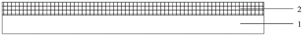
其中附图标记为:1、衬底基板;2、遮光层;3、阻挡层;31、钛膜层;4、缓冲层;5、多晶硅膜层。The reference signs are: 1, base substrate; 2, light shielding layer; 3, barrier layer; 31, titanium film layer; 4, buffer layer; 5, polysilicon film layer.
具体实施方式Detailed ways
为使本领域技术人员更好地理解本发明的技术方案,下面结合附图和具体实施方式对本发明作进一步详细描述。In order to make those skilled in the art better understand the technical solutions of the present invention, the present invention will be further described in detail below with reference to the accompanying drawings and specific embodiments.
实施例1:Example 1:
如图1所示,本实施例提供一种阵列基板的制备方法,其包括在衬底基板上形成遮光图案和位于遮光层上方的薄膜晶体管的各层结构;其中,薄膜晶体管为顶栅型薄膜晶体管,遮光层的位置与薄膜晶体管的有源层的位置相对应。而特别的是,本实施例中的遮光图案层和薄膜晶体管的有源层采用以下工艺制备。As shown in FIG. 1 , the present embodiment provides a method for preparing an array substrate, which includes forming a light-shielding pattern on a base substrate and various layer structures of thin film transistors located above the light-shielding layer; wherein, the thin film transistors are top-gate thin films For transistors, the position of the light shielding layer corresponds to the position of the active layer of the thin film transistor. In particular, the light-shielding pattern layer and the active layer of the thin film transistor in this embodiment are prepared by the following processes.
S11、在衬底基板上形成遮光层。S11, forming a light shielding layer on the base substrate.
S12、在遮光层上方,通过溅射工艺形成阻挡层。S12 , forming a barrier layer above the light shielding layer by a sputtering process.
S13、在阻挡层上方形成半导体材料层。S13, forming a semiconductor material layer over the barrier layer.
S14、通过一次构图工艺,形成包括遮光图案、阻挡图案,以及有源层的图形。S14, a pattern including a light shielding pattern, a blocking pattern, and an active layer is formed through a patterning process.
其中,“构图工艺”是指通过将完整材料层中的一部分除去,从而使该层剩余部分形成所需结构的技术,其通常包括形成材料层、涂布光刻胶、曝光、显影、刻蚀、光刻胶剥离等步骤中的一部或多步。Among them, "patterning process" refers to the technology of removing a part of the complete material layer, so that the remaining part of the layer forms a desired structure, which usually includes forming a material layer, coating photoresist, exposing, developing, etching , one or more of steps such as photoresist stripping.
由于本实施例提供的阵列基板的制备方法,在形成遮光层后,通过溅射工艺在阵列基板上形成阻挡层,因此,在后续形成半导体材料层时,阵列基板在PECVD腔室中不会产生弧光放电的现象,而且在本实施例的制备方法中,采用一次构图工艺形成包括遮光图案和有源层的图形,因此,不但可以减少工艺步骤,而且在工艺过程中不会对阵列基板的性能产生影响。In the method for preparing an array substrate provided in this embodiment, after the light shielding layer is formed, a barrier layer is formed on the array substrate through a sputtering process. Therefore, when the semiconductor material layer is subsequently formed, the array substrate will not be generated in the PECVD chamber. The phenomenon of arc discharge, and in the preparation method of this embodiment, a patterning process is used to form the pattern including the light-shielding pattern and the active layer, so not only can the process steps be reduced, but also the performance of the array substrate is not affected during the process. make an impact.
实施例2:Example 2:
如图2至图8所示,本实施例提供一种阵列基板的制备方法。其中,阵列基板可以为用于液晶显示的阵列基板中,也可以用于有机电致发光二极管阵列基板中。阵列基板中的薄膜晶体管可以为低温多晶硅薄膜晶体管、非晶硅薄膜晶体管、金属氧化物薄膜晶体管的任意一种。As shown in FIG. 2 to FIG. 8 , this embodiment provides a method for fabricating an array substrate. Wherein, the array substrate can be used in an array substrate for liquid crystal display, and can also be used in an organic electroluminescent diode array substrate. The thin film transistors in the array substrate can be any one of low temperature polysilicon thin film transistors, amorphous silicon thin film transistors, and metal oxide thin film transistors.
具体的,以下以阵列基板上包括低温多晶硅薄膜晶体管的制备方法为例进行介绍,本实施例中的制备方法具体包括以下步骤:Specifically, the following takes the preparation method of the low-temperature polysilicon thin film transistor on the array substrate as an example to introduce. The preparation method in this embodiment specifically includes the following steps:
S21、如图3所示,在衬底基板1上形成遮光层2。S21 , as shown in FIG. 3 , a
其中,衬底基板1可以为玻璃基板,遮光层2的材料可以为金属,例如钼(Mo)。具体的,本步骤中,可以通过溅射等工艺在衬底基板1上形成遮光层2。Wherein, the
S22、如图4所示,在遮光层2上方,通过溅射工艺形成阻挡层3。S22 , as shown in FIG. 4 , above the
其中,阻挡层3具有较高的电阻率。本步骤中,通过溅射工艺在衬底基板1上形成覆盖遮光层2的高电阻率的阻挡层3,从而可以在后续制备过程中,避免因覆盖有整面金属层的衬底基板1直接进入PECVD腔室中而发生弧光放电现象,导致最终制备完成的阵列基板的性能不佳。Among them, the
在此需要说明的是,本实施例中,“通过溅射工艺形成阻挡层3”指形成阻挡层3的工艺包括溅射工艺,并不用于限制通过溅射工艺可以直接形成阻挡层3。It should be noted here that, in this embodiment, "forming the
优选的,本实施例中的阻挡层3的材料包括二氧化钛(TiO2)。也即,可利用二氧化钛作为阻挡层3。具体的,当利用二氧化钛作为阻挡层3时,本步骤具体包括:Preferably, the material of the
S221、如图5所示,在遮光层2上形成钛膜层31。具体可通过溅射工艺在形成遮光层2的衬底基板1上沉积一层钛膜层31。S221 , as shown in FIG. 5 , a
优选的,本步骤中钛膜层31的厚度范围在100至200埃米之间。之所以这样设置是因为,通过测试不同厚度的钛膜层31氧化前后的电阻值(实验数据详见表1),发现当钛膜层31的厚度在100至200埃米之间时,其氧化后形成的二氧化钛膜层31的电阻值较大,故可以利用其作为阻挡层3,从而避免阵列基板在PECVD腔室发生弧光放电现象。Preferably, the thickness of the
表1.不同厚度钛膜层31氧化前后电阻值对应表Table 1. Corresponding table of resistance values before and after oxidation of


在此需要说明的是,表1中-9999表示被测物的电阻值超出了测量范围,此种情况可以认为其具有较大的电阻值,近似于绝缘体。It should be noted here that -9999 in Table 1 indicates that the resistance value of the measured object exceeds the measurement range. In this case, it can be considered that it has a large resistance value and is similar to an insulator.
S222、如图6所示,通过退火氧化工艺,使钛膜层31形成阻挡层3。S222 , as shown in FIG. 6 , a
即对钛膜层31进行氧化处理,以使其氧化成为二氧化钛膜层31,从而形成阻挡层3。具体的,可将形成有遮光层2的衬底基板1放置于退火炉中,在氧气或者空气中进行退火,使钛膜层31氧化,形成一层二氧化钛膜层31,以得到所需的阻挡层3。That is, the
优选的,本实施例中,阵列基板的制备方法还包括S23、在阻挡层3上形成缓冲层4。在阻挡层3上形成缓冲层4,可以在后续制备多晶硅膜层5的工艺中,采用ELA(ExcimerLaser Anneal;准分子激光退火)工艺对待晶化非晶硅膜层进行晶化处理时,阻挡热量和氢离子的传递,从而减缓被激光加热的硅的冷却速率,有利于硅的结晶。Preferably, in this embodiment, the preparation method of the array substrate further includes S23 , forming a
具体的,本实施例中,缓冲层4可通过PECVD方法沉积形成。可以理解的是,在利用PECVD方法形成缓冲层4时,由于衬底基板1上形成有阻挡层3,故其不会在PECVD腔室中发生弧光放电。Specifically, in this embodiment, the
优选的,本实施例中,缓冲层4采用氧化硅材料制成,氧化硅材料与硅晶硅材料具有较高的晶格匹配性,在采用ELA工艺形成多晶硅膜层5时,可提高多晶硅膜层5的晶粒质量,并减少多晶硅膜层5与缓冲层4之间的层间缺陷。Preferably, in this embodiment, the
S24、如图7所示,在阻挡层3上方形成多晶硅膜层5。多晶硅膜层5用于在后续构图工艺后形成有源层的图形。S24 , as shown in FIG. 7 , a
具体的,S24可包括:通过PECVD工艺在完成上述步骤的衬底基板1上形成待晶化非晶硅膜层,采用ELA工艺对待晶化非晶硅膜层进行净化处理,使其形成多晶硅膜层5。Specifically, S24 may include: forming an amorphous silicon film layer to be crystallized on the
可以理解的是,根据阵列基板上薄膜晶体管类型的不同,多晶硅膜层5可以相应更改为其它半导体材料层,例如非晶硅膜层、金属氧化物层等。It can be understood that, according to different types of thin film transistors on the array substrate, the
S25、如图8所示,通过一次构图工艺,形成包括遮光图案、阻挡图案,以及有源层的图形。S25 , as shown in FIG. 8 , a pattern including a light-shielding pattern, a blocking pattern, and an active layer is formed through a patterning process.
即通过涂布光刻胶、曝光、显影、刻蚀、光刻胶剥离等步骤,将衬底基板1上的遮光层2、阻挡层3以及多晶硅膜层5中的部分材料一次去除,从而在衬底基板1上形成对应遮光图案、阻挡图案以及有源层的图形。That is, through the steps of coating photoresist, exposing, developing, etching, and peeling off the photoresist, some materials in the
至此,完成本实施例的阵列基板的有源层的制备。So far, the preparation of the active layer of the array substrate of this embodiment is completed.
当然,在完成上述步骤的衬底基板1上还可以依次形成栅绝缘层、栅极、层间绝缘层以及源极、漏极,以完成薄膜晶体管的各层结构,且这几层结构可以采用现有工艺完成,故在此不再详细描述。Of course, a gate insulating layer, a gate electrode, an interlayer insulating layer, a source electrode and a drain electrode can also be formed on the
利用本实施例提供的阵列基板的制备方法制备阵列基板时,可以通过一次构图工艺同时形成包括遮光图案和有源层的图形,且不会对阵列基板的产品良率产生影响。故相对于现有技术,本实施例提供的阵列基板的制备方法可以简化阵列基板的制备工艺,提高生产效率,降低生产成本。When an array substrate is prepared by using the method for preparing an array substrate provided in this embodiment, a pattern including a light-shielding pattern and an active layer can be simultaneously formed through one patterning process without affecting the product yield of the array substrate. Therefore, compared with the prior art, the preparation method of the array substrate provided in this embodiment can simplify the preparation process of the array substrate, improve the production efficiency, and reduce the production cost.
实施例3:Example 3:
本实施例提供一种阵列基板,其可由实施例1或者实施例2中提供的阵列基板的制备方法制备而成。该阵列基板包括:衬底基板;依次设于衬底基板上方的遮光图案、阻挡图案、有源层,且这三者在衬底基板上的正投影完全重合。This embodiment provides an array substrate, which can be prepared by the preparation method of the array substrate provided in
其中,优选的,有源层的材料包括:低温多晶硅、非晶硅、金属氧化物中的任意一种。Wherein, preferably, the material of the active layer includes: any one of low temperature polysilicon, amorphous silicon, and metal oxide.
优选的,阻挡层的材料包括二氧化钛。Preferably, the material of the barrier layer includes titanium dioxide.
本实施例中的阵列基板中,遮光图案、阻挡图案以及有源层可通过一次构图工艺形成,故相对于现有技术,本实施例提供的阵列基板的制备工艺更为简化,生产效率较高,且生产成本较低。In the array substrate in this embodiment, the light-shielding pattern, the blocking pattern and the active layer can be formed through a single patterning process. Therefore, compared with the prior art, the preparation process of the array substrate provided in this embodiment is simpler and the production efficiency is higher , and the production cost is low.
实施例4:Example 4:
本实施例提供一种显示面板,其包括实施例3中提供的任意一种阵列基板。This embodiment provides a display panel including any one of the array substrates provided in
其中,显示装置可以为液晶面板、电子纸、手机、平板电脑、电视机、显示器、笔记本电脑、数码相框、导航仪等任何具有显示功能的产品或部件。Wherein, the display device can be any product or component with display function, such as liquid crystal panel, electronic paper, mobile phone, tablet computer, television, monitor, notebook computer, digital photo frame, navigator, etc.
可以理解的是,以上实施方式仅仅是为了说明本发明的原理而采用的示例性实施方式,然而本发明并不局限于此。对于本领域内的普通技术人员而言,在不脱离本发明的精神和实质的情况下,可以做出各种变型和改进,这些变型和改进也视为本发明的保护范围。It can be understood that the above embodiments are only exemplary embodiments adopted to illustrate the principle of the present invention, but the present invention is not limited thereto. For those skilled in the art, without departing from the spirit and essence of the present invention, various modifications and improvements can be made, and these modifications and improvements are also regarded as the protection scope of the present invention.
Claims (8)
Priority Applications (1)
| Application Number | Priority Date | Filing Date | Title |
|---|---|---|---|
| CN201810003073.4A CN108231794B (en) | 2018-01-02 | 2018-01-02 | Preparation method of array substrate and array substrate |
Applications Claiming Priority (1)
| Application Number | Priority Date | Filing Date | Title |
|---|---|---|---|
| CN201810003073.4A CN108231794B (en) | 2018-01-02 | 2018-01-02 | Preparation method of array substrate and array substrate |
Publications (2)
| Publication Number | Publication Date |
|---|---|
| CN108231794A CN108231794A (en) | 2018-06-29 |
| CN108231794B true CN108231794B (en) | 2020-07-17 |
Family
ID=62642597
Family Applications (1)
| Application Number | Title | Priority Date | Filing Date |
|---|---|---|---|
| CN201810003073.4A Active CN108231794B (en) | 2018-01-02 | 2018-01-02 | Preparation method of array substrate and array substrate |
Country Status (1)
| Country | Link |
|---|---|
| CN (1) | CN108231794B (en) |
Families Citing this family (1)
| Publication number | Priority date | Publication date | Assignee | Title |
|---|---|---|---|---|
| CN110416274B (en) * | 2019-08-02 | 2023-04-07 | 京东方科技集团股份有限公司 | Substrate, preparation method thereof and OLED display panel |
Citations (8)
| Publication number | Priority date | Publication date | Assignee | Title |
|---|---|---|---|---|
| CN101022085A (en) * | 2007-03-12 | 2007-08-22 | 友达光电股份有限公司 | Semiconductor element and manufacturing method thereof |
| CN104538454A (en) * | 2014-12-26 | 2015-04-22 | 深圳市华星光电技术有限公司 | Low-temperature polycrystalline silicon thin film transistor and manufacturing method thereof |
| CN104733540A (en) * | 2009-10-09 | 2015-06-24 | 株式会社半导体能源研究所 | Semiconductor device |
| CN105575819A (en) * | 2016-02-26 | 2016-05-11 | 华南理工大学 | Metal oxide thin film transistor with top gate structure and manufacturing method thereof |
| CN107046042A (en) * | 2017-04-20 | 2017-08-15 | 京东方科技集团股份有限公司 | A kind of low temperature polycrystalline silicon backboard and its manufacture method, display device |
| CN107104110A (en) * | 2017-05-24 | 2017-08-29 | 京东方科技集团股份有限公司 | Array base palte, preparation method, display panel and display device |
| CN107275195A (en) * | 2017-07-18 | 2017-10-20 | 京东方科技集团股份有限公司 | Film pattern method, array base palte and preparation method thereof |
| CN107342260A (en) * | 2017-08-31 | 2017-11-10 | 京东方科技集团股份有限公司 | A kind of low temperature polycrystalline silicon tft array substrate preparation method and array base palte |
-
2018
- 2018-01-02 CN CN201810003073.4A patent/CN108231794B/en active Active
Patent Citations (8)
| Publication number | Priority date | Publication date | Assignee | Title |
|---|---|---|---|---|
| CN101022085A (en) * | 2007-03-12 | 2007-08-22 | 友达光电股份有限公司 | Semiconductor element and manufacturing method thereof |
| CN104733540A (en) * | 2009-10-09 | 2015-06-24 | 株式会社半导体能源研究所 | Semiconductor device |
| CN104538454A (en) * | 2014-12-26 | 2015-04-22 | 深圳市华星光电技术有限公司 | Low-temperature polycrystalline silicon thin film transistor and manufacturing method thereof |
| CN105575819A (en) * | 2016-02-26 | 2016-05-11 | 华南理工大学 | Metal oxide thin film transistor with top gate structure and manufacturing method thereof |
| CN107046042A (en) * | 2017-04-20 | 2017-08-15 | 京东方科技集团股份有限公司 | A kind of low temperature polycrystalline silicon backboard and its manufacture method, display device |
| CN107104110A (en) * | 2017-05-24 | 2017-08-29 | 京东方科技集团股份有限公司 | Array base palte, preparation method, display panel and display device |
| CN107275195A (en) * | 2017-07-18 | 2017-10-20 | 京东方科技集团股份有限公司 | Film pattern method, array base palte and preparation method thereof |
| CN107342260A (en) * | 2017-08-31 | 2017-11-10 | 京东方科技集团股份有限公司 | A kind of low temperature polycrystalline silicon tft array substrate preparation method and array base palte |
Also Published As
| Publication number | Publication date |
|---|---|
| CN108231794A (en) | 2018-06-29 |
Similar Documents
| Publication | Publication Date | Title |
|---|---|---|
| CN107275350B (en) | Array substrate, method for making the same, and display device | |
| CN103123910B (en) | Array base palte and manufacture method, display unit | |
| CN105470197B (en) | The preparation method of low temperature polycrystalline silicon array base palte | |
| CN103700665B (en) | Metal oxide thin-film transistor array base palte and preparation method thereof, display unit | |
| US20160370621A1 (en) | Array substrate, manufacturing method thereof and liquid crystal display | |
| WO2015180269A1 (en) | Array substrate and manufacturing method therefor, and display apparatus | |
| US10008516B2 (en) | LTPS TFT array substrate, its manufacturing method, and display device | |
| JP2011258918A (en) | Display device and method for manufacturing the same | |
| US20160254298A1 (en) | Array Substrate, Manufacturing Method Thereof, and Display Device | |
| CN107482066A (en) | Thin film transistor (TFT) and preparation method thereof, array base palte and display device | |
| US11245037B2 (en) | Method of fabricating array substrate, array substrate, and display apparatus | |
| WO2020177080A1 (en) | Method of forming crystallized semiconductor layer, method of fabricating thin film transistor, thin film transistor, and display apparatus | |
| JP2017508275A (en) | Low temperature polysilicon thin film transistor and method for manufacturing the same | |
| WO2015096307A1 (en) | Oxide thin-film transistor, display device and manufacturing method for array substrate | |
| WO2015165174A1 (en) | Thin film transistor and manufacturing method therefor, display substrate, and display device | |
| WO2017031937A1 (en) | Method for preparing oxide semiconductor thin film and method for preparing thin film transistor | |
| WO2015161619A1 (en) | Thin film transistor and manufacturing method thereof, array substrate and display device | |
| CN105679772A (en) | Manufacturing method of low-temperature polycrystalline silicon TFT substrate and low-temperature polycrystalline silicon TFT substrate | |
| CN105957805A (en) | Manufacturing method of low-temperature polycrystalline silicon thin film, thin film transistor, array substrate and display device | |
| CN105206569A (en) | Array substrate, manufacturing method thereof, display panel and display device | |
| US9651839B2 (en) | Array substrate and manufacturing method thereof, display panel and display device | |
| US20190386143A1 (en) | Thin film transistor array substrate, method of manufacturing the same, and display device including thin film transistor substrate | |
| CN202009000U (en) | Array substrate and liquid crystal display | |
| CN108321208A (en) | Low-temperature polysilicon film transistor and preparation method thereof, array substrate, display device | |
| CN110690232A (en) | Manufacturing method of array substrate, array substrate and display panel |
Legal Events
| Date | Code | Title | Description |
|---|---|---|---|
| PB01 | Publication | ||
| PB01 | Publication | ||
| SE01 | Entry into force of request for substantive examination | ||
| SE01 | Entry into force of request for substantive examination | ||
| GR01 | Patent grant | ||
| GR01 | Patent grant |