JP2014186200A - Electro-optic device and electronic apparatus - Google Patents
Electro-optic device and electronic apparatus Download PDFInfo
- Publication number
- JP2014186200A JP2014186200A JP2013061550A JP2013061550A JP2014186200A JP 2014186200 A JP2014186200 A JP 2014186200A JP 2013061550 A JP2013061550 A JP 2013061550A JP 2013061550 A JP2013061550 A JP 2013061550A JP 2014186200 A JP2014186200 A JP 2014186200A
- Authority
- JP
- Japan
- Prior art keywords
- electrode
- electro
- optical device
- pad
- vct
- Prior art date
- Legal status (The legal status is an assumption and is not a legal conclusion. Google has not performed a legal analysis and makes no representation as to the accuracy of the status listed.)
- Pending
Links
Images


Classifications
-
- H—ELECTRICITY
- H10—SEMICONDUCTOR DEVICES; ELECTRIC SOLID-STATE DEVICES NOT OTHERWISE PROVIDED FOR
- H10D—INORGANIC ELECTRIC SEMICONDUCTOR DEVICES
- H10D89/00—Aspects of integrated devices not covered by groups H10D84/00 - H10D88/00
- H10D89/60—Integrated devices comprising arrangements for electrical or thermal protection, e.g. protection circuits against electrostatic discharge [ESD]
-
- H—ELECTRICITY
- H04—ELECTRIC COMMUNICATION TECHNIQUE
- H04N—PICTORIAL COMMUNICATION, e.g. TELEVISION
- H04N13/00—Stereoscopic video systems; Multi-view video systems; Details thereof
- H04N13/30—Image reproducers
- H04N13/332—Displays for viewing with the aid of special glasses or head-mounted displays [HMD]
- H04N13/344—Displays for viewing with the aid of special glasses or head-mounted displays [HMD] with head-mounted left-right displays
-
- H—ELECTRICITY
- H10—SEMICONDUCTOR DEVICES; ELECTRIC SOLID-STATE DEVICES NOT OTHERWISE PROVIDED FOR
- H10K—ORGANIC ELECTRIC SOLID-STATE DEVICES
- H10K50/00—Organic light-emitting devices
- H10K50/80—Constructional details
- H10K50/84—Passivation; Containers; Encapsulations
-
- H—ELECTRICITY
- H10—SEMICONDUCTOR DEVICES; ELECTRIC SOLID-STATE DEVICES NOT OTHERWISE PROVIDED FOR
- H10K—ORGANIC ELECTRIC SOLID-STATE DEVICES
- H10K59/00—Integrated devices, or assemblies of multiple devices, comprising at least one organic light-emitting element covered by group H10K50/00
- H10K59/10—OLED displays
- H10K59/12—Active-matrix OLED [AMOLED] displays
- H10K59/131—Interconnections, e.g. wiring lines or terminals
-
- G—PHYSICS
- G02—OPTICS
- G02B—OPTICAL ELEMENTS, SYSTEMS OR APPARATUS
- G02B27/00—Optical systems or apparatus not provided for by any of the groups G02B1/00 - G02B26/00, G02B30/00
- G02B27/01—Head-up displays
- G02B27/017—Head mounted
- G02B2027/0178—Eyeglass type
-
- G—PHYSICS
- G02—OPTICS
- G02F—OPTICAL DEVICES OR ARRANGEMENTS FOR THE CONTROL OF LIGHT BY MODIFICATION OF THE OPTICAL PROPERTIES OF THE MEDIA OF THE ELEMENTS INVOLVED THEREIN; NON-LINEAR OPTICS; FREQUENCY-CHANGING OF LIGHT; OPTICAL LOGIC ELEMENTS; OPTICAL ANALOGUE/DIGITAL CONVERTERS
- G02F1/00—Devices or arrangements for the control of the intensity, colour, phase, polarisation or direction of light arriving from an independent light source, e.g. switching, gating or modulating; Non-linear optics
- G02F1/01—Devices or arrangements for the control of the intensity, colour, phase, polarisation or direction of light arriving from an independent light source, e.g. switching, gating or modulating; Non-linear optics for the control of the intensity, phase, polarisation or colour
- G02F1/13—Devices or arrangements for the control of the intensity, colour, phase, polarisation or direction of light arriving from an independent light source, e.g. switching, gating or modulating; Non-linear optics for the control of the intensity, phase, polarisation or colour based on liquid crystals, e.g. single liquid crystal display cells
- G02F1/133—Constructional arrangements; Operation of liquid crystal cells; Circuit arrangements
- G02F1/136—Liquid crystal cells structurally associated with a semi-conducting layer or substrate, e.g. cells forming part of an integrated circuit
- G02F1/1362—Active matrix addressed cells
- G02F1/136204—Arrangements to prevent high voltage or static electricity failures
Landscapes
- Engineering & Computer Science (AREA)
- Multimedia (AREA)
- Signal Processing (AREA)
- Microelectronics & Electronic Packaging (AREA)
- Physics & Mathematics (AREA)
- Optics & Photonics (AREA)
- Electroluminescent Light Sources (AREA)
- Devices For Indicating Variable Information By Combining Individual Elements (AREA)
- Control Of Indicators Other Than Cathode Ray Tubes (AREA)
- Control Of El Displays (AREA)
Abstract
【課題】従来に比べてより効率的に静電気を逃がすことができる電気光学装置、及び電子機器等を提供する。
【解決手段】電気光学装置100は、パッド300と、複数の有機発光ダイオード215と、各有機発光ダイオード215のカソードに共通に電気的に接続されるVCT電極250と、一端がパッド300に電気的に接続され、他端がVCT電極250に電気的に接続される保護素子312とを含む。パッド300は、電気光学装置100が形成される基板の外周辺のうち少なくとも3辺のそれぞれに沿って配置されてもよいし、該基板の外周辺に沿って配置される複数のパッドの1つとして配置されてもよい。
【選択図】図5An electro-optical device, an electronic apparatus, and the like that can release static electricity more efficiently than conventional ones.
An electro-optical device 100 includes a pad 300, a plurality of organic light emitting diodes 215, a VCT electrode 250 electrically connected in common to the cathode of each organic light emitting diode 215, and one end electrically connected to the pad 300. And a protection element 312 having the other end electrically connected to the VCT electrode 250. The pad 300 may be disposed along each of at least three sides of the outer periphery of the substrate on which the electro-optical device 100 is formed, or one of a plurality of pads disposed along the outer periphery of the substrate. May be arranged.
[Selection] Figure 5
Description
本発明は、電気光学装置、及び電子機器等に関し、例えば電気光学素子として有機発光ダイオードを用いた電気光学装置、及びこれを含む電子機器等に関する。 The present invention relates to an electro-optical device, an electronic apparatus, and the like, for example, an electro-optical apparatus using an organic light emitting diode as an electro-optical element, and an electronic apparatus including the same.
近年、有機発光ダイオード(Organic Light Emitting Diode:以下、OLED)等の発光素子を電気光学素子として用いた電気光学装置に関する技術が種々提案されている。この種の電気光学装置では、複数の走査線と複数のデータ線とが交差して配置されると共に、走査線とデータ線の交差に対応して複数の画素回路がマトリックス状に配置される。各画素回路は、少なくとも駆動トランジスター及び発光素子を有し、画素の階調レベルに対応したデータ信号が駆動トランジスターのゲートに供給されると、該駆動トランジスターは、そのゲート・ソース間電圧に応じた電流を発光素子に供給する。発光素子は、駆動トランジスターからの電流に応じた輝度で発光する。 In recent years, various technologies relating to electro-optical devices using light-emitting elements such as organic light emitting diodes (hereinafter referred to as OLEDs) as electro-optical elements have been proposed. In this type of electro-optical device, a plurality of scanning lines and a plurality of data lines are arranged so as to intersect with each other, and a plurality of pixel circuits are arranged in a matrix corresponding to the intersection of the scanning lines and the data lines. Each pixel circuit has at least a driving transistor and a light emitting element. When a data signal corresponding to the gradation level of the pixel is supplied to the gate of the driving transistor, the driving transistor corresponds to the voltage between the gate and the source. A current is supplied to the light emitting element. The light emitting element emits light with a luminance corresponding to the current from the driving transistor.
このような電気光学装置は、例えば電子ビューファインダー(Electronic View Finder:以下、EVF)やヘッドマウントディスプレイ(Head Mounted Display:以下、HMD)等の超小型ディスプレイへの応用に好適な装置である。この場合、電気光学装置には、1画素当たりのサイズをできるだけ小さくしながら画素数を増大させ、限られた画面サイズでより高品質の画像を表示することが要求される。そのため、電気光学装置が形成される半導体基板(チップ)のサイズは、大きくなる傾向にある。 Such an electro-optical device is suitable for application to an ultra-small display such as an electronic view finder (hereinafter referred to as EVF) or a head mounted display (hereinafter referred to as HMD). In this case, the electro-optic device is required to display a higher quality image with a limited screen size by increasing the number of pixels while reducing the size per pixel as much as possible. Therefore, the size of the semiconductor substrate (chip) on which the electro-optical device is formed tends to increase.
その一方で、この種の電気光学装置においても、静電気放電(Electro Static Discharge:以下、ESD)による損傷や誤動作発生等を防止する静電破壊対策は重要であり、電気光学装置における静電破壊対策に関する技術が種々提案されている。例えば、特許文献1には、ESDから半導体回路を保護する保護回路を、該半導体回路と半導体回路に信号で供給するための入力端子との間に配置した半導体装置を含む電気光学装置が開示されている。
On the other hand, in this type of electro-optical device, it is important to take measures against electrostatic breakdown to prevent damage or malfunction due to electrostatic discharge (ESD). Various techniques have been proposed. For example,
例えば特許文献1に開示されているように、ESDから半導体回路等を保護する保護回路は、端子から侵入した静電気を、半導体回路等の高電位側電源電圧が供給される電源線又は該半導体回路の接地電圧が供給される電源線に逃がすように構成される。
For example, as disclosed in
しかしながら、このような手法では、電気光学装置が形成される半導体基板のサイズが大きくなると、基板の外周辺に沿って配置される端子(パッド)によっては、上記の高電位側電源電圧又は接地電圧が供給される端子との距離が遠くなる。 However, in such a method, when the size of the semiconductor substrate on which the electro-optical device is formed increases, depending on the terminals (pads) arranged along the outer periphery of the substrate, the high-potential-side power supply voltage or ground voltage The distance to the terminal to which is supplied is increased.
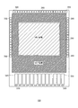
図16に、一般的な電気光学装置における静電破壊対策の説明図を示す。図16は、電気光学装置の端子の配置を模式的に示した平面図を表す。 FIG. 16 is an explanatory diagram of countermeasures against electrostatic breakdown in a general electro-optical device. FIG. 16 is a plan view schematically showing the arrangement of terminals of the electro-optical device.
電気光学装置10は、半導体基板上に形成され、該半導体基板には、複数の画素回路がマトリックス状に配置される表示部12と、基板の外周辺に沿って配置される複数のパッド14とが設けられる。表示部12を構成する画素回路には、複数のパッド14のいずれかを介して外部から制御信号や電源電圧が供給される。
The electro-
なお、電気光学装置10が、表示部12を構成する画素回路に駆動信号を供給する駆動回路を備える場合、該駆動回路は表示部12と複数のパッド14との間に配置され、複数のパッド14には、駆動回路を制御するための各種信号や電源電圧が外部から供給される。
In the case where the electro-
複数のパッド14のうちパッド14aは、表示部12を挟んで対向する位置に配置されるパッド14bから最も遠い。例えばパッド14bが、外部から高電位側電源電圧又は接地電圧が供給される電源パッドであるものとすると、パッド14aの近傍に配置される静電気保護回路16aは、パッド14bとの間で長い配線18を介して接続される。このとき、配線18のインピーダンスが高くなり、パッド14aから侵入する静電気を効率的に電源パッド14bに逃がすことができないケースが懸念される。配線18を表示部12の厚さ方向の上部又は下部に配置することも考えられるが、いずれの場合も配線18のインピーダンスが高くなり、同様のケースが懸念される。
Of the plurality of
本発明は、以上のような技術的課題に鑑みてなされたものである。本発明の幾つかの態様によれば、従来に比べてより効率的に静電気を逃がすことができる電気光学装置、及び電子機器等を提供することができる。 The present invention has been made in view of the above technical problems. According to some aspects of the present invention, it is possible to provide an electro-optical device, an electronic apparatus, and the like that can release static electricity more efficiently than in the past.
(1)本発明の第1の態様は、電気光学装置が、パッドと、複数の有機発光ダイオードと、前記複数の有機発光ダイオードを構成する各有機発光ダイオードのカソードに共通に電気的に接続される第1の電極と、一端が前記パッドに電気的に接続され、他端が前記第1の電極に電気的に接続される第1の保護素子とを含む。 (1) In the first aspect of the present invention, the electro-optical device is electrically connected in common to a pad, a plurality of organic light emitting diodes, and a cathode of each organic light emitting diode constituting the plurality of organic light emitting diodes. A first electrode having one end electrically connected to the pad and the other end electrically connected to the first electrode.
本態様においては、複数の有機発光ダイオードを備えた電気光学装置が、各有機発光ダイオードのカソードに共通に接続される第1の電極と、パッドとの間に接続された第1の保護素子を含んで構成される。これにより、電気光学装置のサイズ(又は電気光学装置が形成される基板のサイズ)が大きくなった場合でも、第1の保護素子と第1の電極とを従来より短い接続配線で接続した状態で、より低いインピーダンスを有する第1の電極に静電気を逃がすことができる。この結果、本態様によれば、従来に比べてより効率的に静電気を逃がすことができる電気光学装置を提供することができる。 In this aspect, an electro-optical device including a plurality of organic light emitting diodes includes a first protective element connected between a first electrode commonly connected to the cathode of each organic light emitting diode and a pad. Consists of including. As a result, even when the size of the electro-optical device (or the size of the substrate on which the electro-optical device is formed) is increased, the first protective element and the first electrode are connected with a shorter connection wiring than before. Static electricity can be released to the first electrode having a lower impedance. As a result, according to this aspect, it is possible to provide an electro-optical device that can release static electricity more efficiently than in the past.
(2)本発明の第2の態様に係る電気光学装置では、第1の態様において、前記第1の保護素子は、保護ダイオード、オフトランジスター、及びサイリスターのうちのいずれかである。 (2) In the electro-optical device according to the second aspect of the invention, in the first aspect, the first protection element is any one of a protection diode, an off-transistor, and a thyristor.
本態様によれば、第1の保護素子として保護ダイオード、オフトランジスター、及びサイリスターのうちのいずれかを採用するようにしたので、第1の保護素子に接続される電極を変更するだけで、従来に比べてより効率的に静電気を逃がすことができる。 According to this aspect, since any one of the protection diode, the off-transistor, and the thyristor is employed as the first protection element, it is possible to simply change the electrode connected to the first protection element. Static electricity can be released more efficiently than.
(3)本発明の第3の態様に係る電気光学装置は、第1の態様又は第2の態様において、それぞれが前記各有機発光ダイオードに電流を供給する複数の駆動トランジスターと、前記複数の駆動トランジスターを構成する各駆動トランジスターのソースに共通に電気的に接続される第2の電極と、一端が前記パッドに電気的に接続され、他端が前記第2の電極に電気的に接続される第2の保護素子とを含む。 (3) The electro-optical device according to a third aspect of the present invention is the electro-optical device according to the first aspect or the second aspect, wherein a plurality of driving transistors each supply current to the organic light emitting diodes, and the plurality of driving A second electrode commonly connected to the source of each driving transistor constituting the transistor, one end electrically connected to the pad, and the other end electrically connected to the second electrode A second protection element.
本態様においては、電気光学装置が、各有機発光ダイオードに電流を供給する各駆動トランジスターのソースに共通に接続される第2の電極と、パッドとの間に接続された第2の保護素子を更に含んで構成される。これにより、電気光学装置のサイズ(又は電気光学装置が形成される基板のサイズ)が大きくなった場合でも、第2の保護素子を介して、より低いインピーダンスを有する第2の電極に静電気を逃がすことができる。この結果、本態様によれば、従来に比べてより効率的に静電気を逃がすことができる電気光学装置を提供することができる。 In this aspect, the electro-optical device includes a second protective element connected between the second electrode connected in common to the source of each driving transistor that supplies current to each organic light emitting diode and the pad. Furthermore, it is comprised. Accordingly, even when the size of the electro-optical device (or the size of the substrate on which the electro-optical device is formed) is increased, static electricity is released to the second electrode having a lower impedance via the second protective element. be able to. As a result, according to this aspect, it is possible to provide an electro-optical device that can release static electricity more efficiently than in the past.
(4)本発明の第4の態様に係る電気光学装置では、第3の態様において、前記第2の保護素子は、保護ダイオード、又はオフトランジスターである。 (4) In the electro-optical device according to the fourth aspect of the present invention, in the third aspect, the second protection element is a protection diode or an off-transistor.
本態様によれば、第2の保護素子として保護ダイオード又はオフトランジスターを採用するようにしたので、第2の保護素子に接続される電極を変更するだけで、従来に比べてより効率的に静電気を逃がすことができる。 According to this aspect, since the protection diode or the off-transistor is employed as the second protection element, the static electricity is more efficiently compared to the conventional case only by changing the electrode connected to the second protection element. Can escape.
(5)本発明の第5の態様に係る電気光学装置では、第3の態様又は第4の態様において、前記第2の電極は、前記複数の有機発光ダイオードが形成される表示領域に平面視で重なるように配置され、前記第1の電極は、前記第2の電極を周回するように配置される1又は複数の電極により構成される。 (5) In the electro-optical device according to the fifth aspect of the present invention, in the third aspect or the fourth aspect, the second electrode is planarly viewed in a display region in which the plurality of organic light emitting diodes are formed. The first electrode is composed of one or a plurality of electrodes arranged so as to go around the second electrode.
本態様によれば、表示領域を有効活用して配置されるため、第1の電極及び第2の電極のそれぞれのインピーダンスがより一層低くなり、パッドから侵入した静電気をより一層効率よく逃がすことができるようになる。 According to this aspect, since the display area is effectively utilized, the impedance of each of the first electrode and the second electrode is further reduced, and static electricity that has entered from the pad can be released more efficiently. become able to.
(6)本発明の第6の態様に係る電気光学装置では、第3の態様又は第4の態様において、前記第2の電極は、前記複数の有機発光ダイオードが形成される表示領域に平面視で重なるように配置され、前記第1の電極は、前記第2の電極の外周辺のうち互いに交差する2辺に沿った外周辺を有する。 (6) In the electro-optical device according to the sixth aspect of the present invention, in the third aspect or the fourth aspect, the second electrode is planarly viewed in a display region where the plurality of organic light emitting diodes are formed. The first electrode has an outer periphery along two sides that intersect each other among the outer periphery of the second electrode.
ここで、第2の電極が矩形形状を有する場合、第1の電極は、第2の電極の外周辺の3辺に沿った外周辺を有していてもよい。本態様によれば、表示領域を有効活用して配置されるため、第1の電極及び第2の電極のそれぞれのインピーダンスがより一層低くなり、パッドから侵入した静電気をより一層効率よく逃がすことができるようになる。 Here, when the second electrode has a rectangular shape, the first electrode may have an outer periphery along three sides of the outer periphery of the second electrode. According to this aspect, since the display area is effectively utilized, the impedance of each of the first electrode and the second electrode is further reduced, and static electricity that has entered from the pad can be released more efficiently. become able to.
(7)本発明の第7の態様に係る電気光学装置は、第3の態様乃至第6の態様のいずれかにおいて、前記第2の電極と前記第2の保護素子の他端とを電気的に接続する接続配線を含み、前記接続配線は、前記第1の電極と平面視で重なるように配置される。 (7) An electro-optical device according to a seventh aspect of the present invention is the electro-optical device according to any one of the third to sixth aspects, in which the second electrode and the other end of the second protection element are electrically connected. The connection wiring is arranged to overlap the first electrode in plan view.
本態様においては、第2の電極の外側に第1の電極が配置されるため第1の電極と第1の保護素子との間は最短距離で接続することができる。そして、更に、その内部に配置される第2の電極と第2の保護素子とを接続する接続配線を、第1の電極と平面視で重なるように配置することで、第2の電極と第2の保護素子との間は最短距離で接続することで、より効率よく静電気を逃がすことができる。 In this aspect, since the first electrode is disposed outside the second electrode, the first electrode and the first protective element can be connected with the shortest distance. Further, by disposing a connection wiring for connecting the second electrode and the second protection element disposed therein so as to overlap the first electrode in plan view, the second electrode and the second electrode Static electricity can be released more efficiently by connecting the two protective elements with the shortest distance.
(8)本発明の第8の態様に係る電気光学装置では、第1の態様乃至第7の態様のいずれかにおいて、接地電圧が供給される電源パッドを含み、前記第1の電極と前記第1の保護素子とを接続する配線のインピーダンスと前記第1の電極のインピーダンスとの合成インピーダンスが、前記電源パッドに電気的に接続される配線のインピーダンスより低い。 (8) In an electro-optical device according to an eighth aspect of the present invention, the electro-optical device according to any one of the first to seventh aspects includes a power supply pad to which a ground voltage is supplied, and the first electrode and the first electrode The combined impedance of the impedance of the wiring connecting one protection element and the impedance of the first electrode is lower than the impedance of the wiring electrically connected to the power supply pad.
本態様によれば、第1の電極と第1の保護素子とを接続する配線のインピーダンスと第1の電極のインピーダンスとの合成インピーダンスが、電源電圧が供給される電源パッドに接続される配線のインピーダンスより低くなるようにしたので、従来に比べてより効率的に静電気を逃がすことができる電気光学装置を提供することができる。 According to this aspect, the combined impedance of the impedance of the wiring connecting the first electrode and the first protection element and the impedance of the first electrode is equal to the wiring connected to the power supply pad to which the power supply voltage is supplied. Since the impedance is lower than the impedance, it is possible to provide an electro-optical device that can release static electricity more efficiently than in the past.
(9)本発明の第9の態様に係る電気光学装置では、第1の態様乃至第8の態様のいずれかにおいて、前記パッドは、前記電気光学装置が形成される基板の外周辺に沿って配置される複数のパッドの1つである。 (9) In the electro-optical device according to the ninth aspect of the present invention, in any one of the first to eighth aspects, the pad extends along the outer periphery of the substrate on which the electro-optical device is formed. One of a plurality of pads to be arranged.
本態様によれば、基板の外周辺に沿って複数のパッドが配置される場合に、基板のサイズが大きくなっても、従来に比べてより効率的に静電気を逃がすことができる電気光学装置を提供することができる。 According to this aspect, when a plurality of pads are arranged along the outer periphery of the substrate, the electro-optical device can discharge static electricity more efficiently than the conventional case even when the size of the substrate is increased. Can be provided.
(10)本発明の第10の態様に係る電気光学装置では、第1の態様乃至第8の態様のいずれかにおいて、前記電気光学装置が形成される基板の外周辺のうち少なくとも3辺のそれぞれに沿って前記パッドが配置される。 (10) In the electro-optical device according to the tenth aspect of the present invention, in any one of the first to eighth aspects, each of at least three sides of the outer periphery of the substrate on which the electro-optical device is formed The pad is disposed along the line.
本態様によれば、基板の外周辺のうち少なくとも3辺のそれぞれに沿って複数のパッドが配置される場合に、基板のサイズが大きくなっても、従来に比べてより効率的に静電気を逃がすことができる電気光学装置を提供することができる。 According to this aspect, when a plurality of pads are arranged along each of at least three sides of the outer periphery of the substrate, the static electricity is released more efficiently than the conventional case even if the size of the substrate is increased. An electro-optical device that can be provided can be provided.
(11)本発明の第11の態様に係る電気光学装置では、第1の態様乃至第10の態様のいずれかにおいて、前記パッドは、前記電気光学装置の実装用パッドである。 (11) In the electro-optical device according to the eleventh aspect of the present invention, in any one of the first to tenth aspects, the pad is a mounting pad for the electro-optical device.
本態様によれば、表示モジュール等に実装するため実装用パッドから侵入する静電気を従来より効率よく逃がすことができる電気光学装置を提供することができる。 According to this aspect, it is possible to provide an electro-optical device that can efficiently dissipate static electricity entering from a mounting pad for mounting on a display module or the like.
(12)本発明の第12の態様は、電子機器が、第1の態様乃至第11の態様のいずれかの電気光学装置を含む。 (12) In a twelfth aspect of the present invention, the electronic apparatus includes the electro-optical device according to any one of the first to eleventh aspects.
本態様によれば、パッドから侵入する静電気を従来より効率よく逃がすことができる電気光学装置が適用された電子機器を提供することができる。 According to this aspect, it is possible to provide an electronic apparatus to which an electro-optical device that can efficiently discharge static electricity entering from a pad is more than conventional.
以下、本発明の実施の形態について図面を用いて詳細に説明する。なお、以下に説明する実施の形態は、特許請求の範囲に記載された本発明の内容を不当に限定するものではない。また以下で説明される構成のすべてが本発明の課題を解決するために必須の構成要件であるとは限らない。 Hereinafter, embodiments of the present invention will be described in detail with reference to the drawings. The embodiments described below do not unduly limit the contents of the present invention described in the claims. In addition, all of the configurations described below are not necessarily indispensable configuration requirements for solving the problems of the present invention.
〔電気光学装置〕
図1に、本発明の一実施形態に係る電気光学装置の構成の概要を示す。
本実施形態における電気光学装置100は、発光素子としてOLEDが用いられる複数の画素回路や各画素回路に駆動信号等を供給する駆動回路等が、例えばシリコン基板に形成された有機EL装置である。
Electro-optical device
FIG. 1 shows an outline of the configuration of an electro-optical device according to an embodiment of the invention.
The electro-
電気光学装置100は、走査線駆動回路110と、データ線駆動回路120と、表示部200とを備えている。電気光学装置100の外部には、制御回路150と、電源回路160とが設けられる。
電気光学装置100は、走査線駆動回路110及びデータ線駆動回路120のうち少なくとも1つが外部に設けられた構成を有していてもよい。また、電気光学装置100は、制御回路150及び電源回路160の少なくとも1つが内蔵された構成を有していてもよい。
The electro-
The electro-
表示部200は、マトリックス状に配列されている複数の画素回路210を備えている。複数の画素回路210は、それぞれが同一の構成を有する。表示部200には、各走査線が図1のX方向に延びるようにm(mは2以上の整数)本の走査線112が配列される。また、表示部200には、各データ線が図1のY方向に延びるようにn(nは2以上の整数)列のデータ線122が配列される。そして、m行の走査線112とn列のデータ線122との交差に対応して、画素回路210が設けられる。1本の走査線112とX方向に隣接する3本のデータ線122との交差に対応した3つの画素回路210は、それぞれR(赤)、G(緑)、及びB(青)の画素に対応し、カラー画像を構成する画素の1ドットを表現する。
The
制御回路150は、走査線駆動回路110及びデータ線駆動回路120に対して制御信号Ctr1,Ctr2を供給すると共に、データ線駆動回路120に対して各行の画素に対応した画像データを供給する。また、制御回路150は、電源回路160による各種の電源電圧の生成を制御することができる。
制御信号Ctr1は、走査線駆動回路110を制御するためのパルス信号である垂直同期信号、水平同期信号、クロック信号やイネーブル信号である。
制御信号Ctr2は、データ線駆動回路120を制御するための水平同期信号、ドットクロック信号DCLK、ラッチパルス信号LPやイネーブル信号である。
画像データは、走査線駆動回路110からの走査信号により選択された行の画素毎の階調レベルに対応したデータである。
The
The control signal Ctr1 is a vertical synchronization signal, a horizontal synchronization signal, a clock signal, and an enable signal that are pulse signals for controlling the scanning
The control signal Ctr2 is a horizontal synchronization signal for controlling the data line driving
The image data is data corresponding to the gradation level for each pixel in the row selected by the scanning signal from the scanning
走査線駆動回路110は、垂直同期信号により規定される各フレーム期間において走査線112を1行毎に順番に走査するための走査信号Gwr(1)〜Gwr(m)を制御信号Ctr1に基づいて生成する。図1では、1,2,3,・・・,(m−1),m行目の走査線112に供給される走査信号を、それぞれGwr(1),Gwr(2),Gwr(3),・・・,Gwr(m−1),Gwr(m)と表記している。
なお、走査線駆動回路110は、走査信号Gwr(1)〜GWr(m)の他に、各画素回路に供給する制御信号を行毎に生成するが、図1では図示を省略している。
The scanning
The scanning
データ線駆動回路120は、水平走査期間毎に、走査線駆動回路110により選択され行の各画素の階調レベルに対応したデータ信号Vd(1)〜Vd(n)を各データ線122に供給する。
The data line driving
電源回路160は、走査線駆動回路110、データ線駆動回路120、及び制御回路150のそれぞれに必要な各種の電源電圧を生成し供給する。
具体的には、電源回路160は、走査線駆動回路110に対し、走査線駆動回路110を動作させるための電源電圧や、走査信号Gwr(1)〜Gwr(m)や各画素回路に供給される制御信号を生成するための各種電源電圧を供給する。
また、電源回路160は、データ線駆動回路120に対し、データ線駆動回路120を動作させるための電源電圧や、階調レベルに対応した複数の階調電圧を供給する。
更に、電源回路160は、表示部200を構成する各画素回路に対し、各画素回路を動作させるための電源電圧を供給する。
The
Specifically, the
The
Further, the
図2に、図1の電気光学装置100の回路平面配置の一例を示す。図2において、図1と同様の部分には同一符号を付し、適宜説明を省略する。
FIG. 2 shows an example of a circuit plane arrangement of the electro-
電気光学装置100が形成される半導体基板(以下では、適宜、基板と略す)では、矩形形状の表示部200の外周辺に沿って、走査線駆動回路110a,110bと、データ線駆動回路120と、図1では図示しないテスト回路130とが配置される。
走査線駆動回路110a,110bは、表示部200の外周辺のうち対向する2辺SD1,SD2のそれぞれに沿って配置される。表示部200の外周辺のうち辺SD1,SD2と交差する辺SD3に沿ってデータ線駆動回路120が配置され、表示部200の外周辺のうち辺SD3に対向する辺SD4に沿ってテスト回路130が配置される。
In a semiconductor substrate (hereinafter, appropriately abbreviated as a substrate) on which the electro-
The scanning
また、電気光学装置100が形成される基板の外周辺のうち対向する辺SD10,SD11と、辺SD10,SD11と交差する辺SD12に沿って複数のパッド300がテスト用パッドとして配置される。各パッド300に対応して各保護回路310が設けられており、各保護回路310は、対応するパッド300の近傍位置で、該パッド300より基板の内部側に配置されている。
In addition, a plurality of
更に、電気光学装置100が形成される基板の外周辺のうち辺SD12に対向する辺SD13に沿って複数の実装用パッド320が配置される。各実装用パッド320に対応して各保護回路330が設けられており、各保護回路330は、対応する実装用パッド320の近傍位置で、該実装用パッド320より基板の端部側に配置されている。なお、保護回路330の構成は、保護回路310の構成と同様である。
Furthermore, a plurality of mounting
走査線駆動回路110a,110bは、それぞれ図1の走査線駆動回路110の機能を有し、同一走査線に対して互いに同一タイミングで走査信号や制御信号を供給する。これにより、表示部200を構成する画素回路210の位置によって走査信号等のなまりに起因した表示ムラを低減する。
Each of the scanning
テスト回路130は、表示部200を構成する複数の画素回路210の動作を検証するための制御を行う。具体的には、テストモード動作時に、テスト回路130は、1又は複数のデータ線122毎に、対応するパッド300を介してデータ信号を出力する制御を行う。これにより、表示部200を構成する複数の画素回路210やこれらに接続されるデータ線122等の検証が可能となる。
The
以上のような構成を有する電気光学装置100において、パッド300に対応して設けられる保護回路310は、表示部200を構成する複数の画素回路210に共通に接続されるVEL電極及びVCT電極の少なくとも一方に静電気を逃がす構成を有している。
In the electro-
以下、本実施形態におけるVEL電極及びVCT電極について説明するため、VEL電極及びVCT電極が接続される画素回路210について説明する。
Hereinafter, in order to describe the VEL electrode and the VCT electrode in the present embodiment, the
図3に、図1の画素回路210の構成例を示す。図3は、i(iは自然数)行目のj(jは自然数)列目に位置する画素回路を表す。図3において、図1と同様の部分には同一符号を付し、適宜説明を省略する。
FIG. 3 shows a configuration example of the
画素回路210は、P型金属酸化膜半導体(Metal-Oxide Semiconductor:以下、MOS)トランジスター211〜214と、OLED215と、保持容量216とを備えている。画素回路210には、トランジスター212〜214のそれぞれのゲート信号となる走査信号Gwr(i)、制御信号Gcmp(i),Gel(i)が供給される。走査信号Gwr(i)、制御信号Gcmp(i),Gel(i)は、i行目に対応して走査線駆動回路110(110a,110b)によって供給された信号であり、i行目のj列以外の他の列の画素回路にも共通に供給される。
The
トランジスター211は、駆動トランジスターとして、ソースがVEL電極250(第2の電極)に電気的に接続され、ドレインがトランジスター213のドレインと、トランジスター214のソースとに電気的に接続される。また、トランジスター211のゲートは、トランジスター212のドレインと、トランジスター213のソースと、保持容量216の一端とに電気的に接続される。VEL電極250には、画素回路210において電源の高電位側となる電圧Velが供給される。電圧Velは、電源回路160から供給される電圧である。
As the driving transistor, the
トランジスター212は、書き込みトランジスターとして、ソースがデータ線122に電気的に接続され、ゲートが走査線112に接続される。トランジスター212のゲートは、ゲート信号としての走査信号Gwr(i)により制御される。
The
トランジスター213は、閾値補償トランジスターとして、ゲートに制御信号Gcmp(i)が供給される。トランジスター213のゲートは、ゲート信号としての制御信号Gcmp(i)により制御される。 The transistor 213 is a threshold compensation transistor, and a control signal Gcmp (i) is supplied to the gate. The gate of the transistor 213 is controlled by a control signal Gcmp (i) as a gate signal.
トランジスター214は、電流供給制御トランジスターとして、ドレインがOLED215のアノードに電気的に接続され、ゲートに制御信号Gel(i)が供給される。トランジスター214のゲートは、ゲート信号としての制御信号Gel(i)により制御される。トランジスター214を設けることにより、例えば電源投入直後にOLED215に電流が供給されて意図しない画像を表示してしまうという事態を回避することができる。
The
また、図3に示すように、トランジスター211〜214の基板電位として、電圧Velが供給される。
更に、画素回路210には、ドレインがOLED215のアノードに電気的に接続され、ソースに所与の初期電圧が供給されるP型MOSトランジスターを設けてもよい。所定のタイミングで、このトランジスターを介して初期電圧をOLED215のアノードに印加することで、OLED215の寄生容量に蓄積された電荷を初期化することができ、OLED215の寄生容量に起因した表示劣化を防止することができるようになる。
Further, as illustrated in FIG. 3, the voltage Vel is supplied as the substrate potential of the
Furthermore, the
OLED215のカソードは、VCT電極260(第1の電極)に電気的に接続され、該カソードには、画素回路210において電源の低電位側である電圧Vctが供給される。OLED215は、基板においてアノードと光透過性を有するカソードとにより白色有機EL層を挟持することにより構成される発光素子であり、出射側であるカソードには、R、G、Bのいずれかのカラーフィルターが重ねて配置されている。OLED215に、アノードからカソードに電流が流れると、アノードから注入された正孔とカソードから注入された電子とが有機EL層において再結合して励起子が生成され、白色光が発光する。この白色光は、カソードを透過後にカラーフィルターにより着色され、観察者に視認される。
The cathode of the
保持容量216の他端は、VEL電極250に電気的に接続され、トランジスター211のゲート・ソース間電圧を保持する。
保持容量216は、トランジスター211のゲートの寄生容量や、絶縁層を導電層で挟持して形成される容量を用いて形成される。
The other end of the
The
図3に示す画素回路210の動作について、簡単に説明すると、走査信号により選択された1水平走査期間内に、階調レベルに対応したデータ信号がトランジスター212を介して書き込まれる。すると、トランジスター213がオンとなり、トランジスター211の閾値が補償された状態で保持容量216にデータ信号が保持される。その後、トランジスター214がオンとなり、OLED215には、トランジスター211のゲート・ソース間電圧に対応した電流が供給される。このため、OLED215は、トランジスター211の閾値を補償した状態で、階調レベルに対応した輝度で発光することができる。
The operation of the
図4に、図3のVEL電極250及びVCT電極260の平面配置の一例を示す。図4において、図2又は図3と同様の部分には同一符号を付し、適宜説明を省略する。
FIG. 4 shows an example of a planar arrangement of the
VEL電極250は、複数のOLEDが形成される表示領域である表示部200に平面視で重なるように配置される。VEL電極250は、複数の実装用パッド320のいずれかに電気的に接続され、この実装用パッド320を介して電圧VelがVEL電極250に供給される。
The
これに対して、VCT電極260は、VEL電極250と電気的に分離された状態で、VEL電極250を周回するように配置される。VCT電極260は、複数の実装用パッド320のいずれかに電気的に接続され、この実装用パッド320を介して電圧VctがVCT電極260に供給される。これにより、表示部200を構成する複数の画素回路210のそれぞれは同一の条件でVEL電極250に接続されるため、表示ムラの低減を図ることができる。
On the other hand, the
なお、電圧Vctは、接地電圧Vssと同電位の電圧とすることができる。しかしながら、本実施形態では、複数の実装用パッド320は、接地電圧Vssを供給するための電源パッドとは別に、電圧Vctを供給するためのパッドを含む。そのため、保護回路310(具体的には、保護回路310を構成する保護素子)とVCT電極260とを接続する配線のインピーダンスとVCT電極260のインピーダンスとの合成インピーダンスを、接地電圧Vssを供給するための電源パッドに電気的に接続される配線のインピーダンスより低くすることができる。
The voltage Vct can be the same potential as the ground voltage Vss. However, in the present embodiment, the plurality of mounting
更に、基板の外周辺に沿って配置されるパッド300の近傍の保護回路310(図4では図示せず)は、従来よりも短い配線を介してVEL電極250又はVCT電極260に電気的に接続される。そのため、本実施形態によれば、従来と比べて、より低いインピーダンスの電極に静電気を効率よく逃がすことができるようになる。
Further, the protection circuit 310 (not shown in FIG. 4) in the vicinity of the
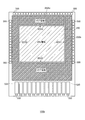
図5に、本実施形態における保護回路310の説明図を示す。図5において、図1〜図4と同一部分には同一符号を付し、適宜説明を省略する。
図6に、図5の保護回路310の構成例の回路図を示す。図6において、図5と同様の部分には同一符号を付し、適宜説明を省略する。
FIG. 5 is an explanatory diagram of the
FIG. 6 shows a circuit diagram of a configuration example of the
本実施形態では、パッド300に接続されその近傍に配置される図2の保護回路310が、上記のVEL電極250及びVCT電極260に接続される。パッド300から侵入した静電気は、従来よりもインピーダンスが低いVEL電極250又はVCT電極260に逃がされ、保護回路310に接続される内部回路を保護する。
In the present embodiment, the
図6に示すように、保護回路310は、保護素子312,314と、保護抵抗316とを備えている。保護素子312(第1の保護素子)の一端は、パッド300に電気的に接続され、他端はVCT電極260に電気的に接続される。保護素子314(第2の保護素子)の一端は、パッド300に電気的に接続され、他端は、VEL電極250に電気的に接続される。
As shown in FIG. 6, the
即ち、電気光学装置100は、パッド300と、複数のOLED215と、各OLED215のカソードに共通に電気的に接続されるVCT電極260と、一端がパッド300に電気的に接続され他端がVCT電極260に電気的に接続される保護素子312とを含むことができる。図6では、保護素子312は、保護ダイオードにより構成され、該保護ダイオードのアノードは、VCT電極260に電気的に接続され、該保護ダイオードのカソードは、パッド300に電気的に接続される。
なお、保護素子312は、オフトランジスター又はサイリスターにより構成されていてもよい。
That is, the electro-
Note that the
更に、電気光学装置100は、複数のトランジスター211と、各トランジスター211のソースに共通に電気的に接続されるVEL電極250と、一端がパッド300に電気的に接続され他端がVEL電極250に接続される保護素子314とを含むことができる。図6では、保護素子314は、保護ダイオードにより構成され、該保護ダイオードのアノードは、パッド300に電気的に接続され、該保護ダイオードのカソードは、VEL電極250に電気的に接続される。
なお、保護素子314は、オフトランジスターにより構成されていてもよい。
Further, the electro-
Note that the
このとき、VCT電極260は、VEL電極250を周回するように配置されるため、図7に示すように、保護回路310を構成する保護素子312の他端とVCT電極260との間は、最短経路の接続配線410により接続されることが望ましい。また、図7に示すように、電気光学装置100は、VEL電極250と保護回路310を構成する保護素子314の他端とを接続する接続配線400を備え、接続配線400は、VCT電極260と平面視で重なるように配置されることが望ましい。こうすることで、保護素子312の他端とVCT電極260との間のみならず、保護素子314の他端とVEL電極250との間を、最短経路で接続することができる。
At this time, since the
図8に、図2のA−A線に沿った電気光学装置100の断面構造の一例を模式的に示す。図8において、図1〜図3と同様の部分には同一符号を付し、適宜説明を省略する。なお、図8は、走査線駆動回路110bを通るA−A線に沿った断面構造の一例を表すが、走査線駆動回路110aを通る線に沿った断面構造も同様である。また、図8において、OLED215の断面構造の詳細については図示を省略している。
FIG. 8 schematically shows an example of a cross-sectional structure of the electro-
電気光学装置100は、P型半導体基板500に形成される。P型半導体基板500には、N型不純物領域(ウェル)502,504やP型不純物領域506,508,510が形成される。N型不純物領域502上に、画素回路210が形成される。N型不純物領域504及びP型不純物領域506,508上に、走査線駆動回路110bを構成する回路の一部が形成される。P型不純物領域510上に、図6に示す保護回路310を構成する保護素子312が形成される。
The electro-
P型半導体基板500の上層に形成されたパッド300は、スルーホールを介して電気的に接続される複数の配線層を介して、P型不純物領域510に形成されるN型高濃度不純物領域512に接続される。このP型不純物領域510には、更にP型高濃度不純物領域514が形成されており、P型高濃度不純物領域514は、スルーホールを介して電気的に接続される複数の配線層を介して、VCT電極260に電気的に接続される。N型高濃度不純物領域512側が保護ダイオードのカソード側となり、P型高濃度不純物領域514側が保護ダイオードのアノード側となる。N型高濃度不純物領域512とP型高濃度不純物領域514により、保護素子312が形成される。なお、図8では図示されていないが、同様にして保護素子314も形成される。
The
VCT電極260は、走査線駆動回路110bを構成するトランジスターの上層に形成される。
The
VEL電極250の下層には、絶縁膜を挟持した導電層からなる容量がスタックされた保持容量216が形成される。この保持容量216の一端は、上層のVEL電極250に電気的に接続され、他端は図示しないトランジスターのゲート等に接続されている。
Under the
VEL電極250は、スルーホールを介して電気的に接続される複数の配線層を介して、N型不純物領域502に形成されるN型高濃度不純物領域516に電気的に接続される。N型不純物領域502には、上層にゲート酸化膜を介してゲート電極が形成されるチャネル領域を挟んでP型アクティブ領域518,520が形成されている。P型アクティブ領域518は、P型トランジスターのソースとなり、P型アクティブ領域520は、P型トランジスターのドレインとなる。P型アクティブ領域520は、スルーホールを介して電気的に接続される複数の配線層を介して、VEL電極250の上層に形成されるOLED215に電気的に接続される。
The
なお、本実施形態では、実装用パッド320の近傍に配置される保護回路330を構成する保護素子は、VEL電極250又はVCT電極260に接続されていない。これは、VEL電極250又はVCT電極260より、実装用パッド320のうち電圧Vel又は電圧Vctが供給されるパッドに接続される電源線に最短距離で接続することができるためである。しかしながら、実装用パッド320についても、パッド300と同様に、その近傍に配置される保護回路330を構成する保護素子を、VEL電極250又はVCT電極260に接続するようにしてもよい。
即ち、本発明に係るパッドは、電気光学装置100が形成される基板の外周辺のうち少なくとも3辺のそれぞれに沿って配置されるが、該基板の外周辺に沿って配置される複数のパッド300の1つ、又は電気光学装置100の実装用パッド320であってもよい。
In the present embodiment, the protection element constituting the
In other words, the pads according to the present invention are arranged along each of at least three sides of the outer periphery of the substrate on which the electro-
以上説明したように、本実施形態では、表示部200に形成される複数のOLEDに共通に接続されるVEL電極250又はVCT電極260を、保護回路310を構成する保護素子に接続するようにした。これにより、電気光学装置100が形成される基板のサイズが大きくなった場合であっても、配線を引き回すことなく、従来に比べてより低いインピーダンスの電極に、パッドから侵入する静電気を効率よく逃がすことができるようになる。
As described above, in this embodiment, the
〔変形例〕
図4では、VCT電極260は、VEL電極250に周回するように配置されていたが、本実施形態におけるVCT電極260の平面形状は、これに限定されるものではない。VCT電極は、VEL電極を周回するように配置される複数の電極に構成されたり、VEL電極の外周辺のうち少なくとも2辺に沿った外周辺を有するように配置されたりしてもよい。
[Modification]
In FIG. 4, the
1. 第1の変形例
図9に、本実施形態の第1の変形例における電気光学装置のVEL電極及びVCT電極の平面配置の一例を示す。図9において、図4と同様の部分には同一符号を付し、適宜説明を省略する。
1. First Modified Example FIG. 9 shows an example of a planar arrangement of the VEL electrode and the VCT electrode of the electro-optical device in the first modified example of the present embodiment. 9, parts that are the same as those in FIG. 4 are given the same reference numerals, and descriptions thereof will be omitted as appropriate.
第1の変形例における電気光学装置100aにおいて配置されるVEL電極及びVCT電極が、図4の電気光学装置100において配置されるVEL電極250及びVCT電極260と異なる点は、平面視におけるVCT電極の形状である。電気光学装置100aでは、VCT電極260aは、矩形形状のVEL電極250の外周辺のうち3辺に沿った外周辺を有し、コ字又はU字の形状を有する。
The VEL electrode and the VCT electrode arranged in the electro-
具体的には、VCT電極260aは、VEL電極250の外周辺のうち対向する辺SD20,SD21と、辺SD20,SD21と交差する辺SD22に沿った外周辺を有する。図9では、辺SD22は、実装用パッド320の配列方向に沿う辺である。VCT電極260aは、複数の実装用パッド320のいずれかに電気的に接続され、この実装用パッド320を介して電圧VctがVCT電極260aに供給される。
Specifically, the
なお、図9では、VCT電極260aの開口側が、辺SD22に対向する辺SD23側に設けられているが、この開口側が、辺SD20,SD21,辺SD22のいずれかの辺側に設けられていてもよい。
In FIG. 9, the opening side of the
第1の変形例によれば、パッド300とVCT電極260aとを接続する配線をより短くでき、且つ、VCT電極260aのインピーダンスをより低くすることができるので、本実施形態と同様に、表示ムラの低減を図ることができる。
According to the first modification, the wiring connecting the
2. 第2の変形例
図10に、本実施形態の第2の変形例における電気光学装置のVEL電極及びVCT電極の平面配置の一例を示す。図10において、図4又は図9と同様の部分には同一符号を付し、適宜説明を省略する。
2. Second Modification FIG. 10 shows an example of a planar arrangement of the VEL electrode and the VCT electrode of the electro-optical device according to the second modification of the present embodiment. 10, parts that are the same as those in FIG. 4 or FIG. 9 are given the same reference numerals, and descriptions thereof will be omitted as appropriate.
第2の変形例における電気光学装置100bにおいて配置されるVEL電極及びVCT電極が、図4の電気光学装置100において配置されるVEL電極250及びVCT電極260と異なる点は、VCT電極が分割されて配置される点である。電気光学装置100bには、VCT電極260b1,260b2が形成され、VCT電極260b1は、図9のVCT電極260aと同様に、図10の矩形形状のVEL電極250の外周辺のうち3辺に沿った外周辺を有し、コ字又はU字の形状を有する。VCT電極260b2は、VEL電極250の外周辺のうち残りの1辺に沿った外周辺を有する。
The VEL electrode and the VCT electrode arranged in the electro-
具体的には、VCT電極260b1は、VEL電極250の外周辺のうち対向する辺SD20,SD21と、辺SD20,SD21と交差する辺SD22に沿った外周辺を有する。VCT電極260b2は、VEL電極250の外周辺のうち辺SD22に対向する辺SD23に沿った外周辺を有する。即ち、VCT電極260b1は、VCT電極260b2の開口側に設けられ、VCT電極260b1,260b2は、対向配置することにより、VEL電極250を周回するように配置される。VCT電極260b1,260b2は、複数の実装用パッド320のいずれかに電気的に接続され、この実装用パッド320を介して電圧VctがVCT電極260b1,260b2に供給される。
Specifically, VCT electrodes 260b 1 includes a side SD20, SD21 opposite of the outer periphery of the
なお、図10では、VCT電極260b1の開口側が、辺SD23側に設けられているが、この開口側が、辺SD20,SD21,辺SD22のいずれかの辺側に設けられていてもよい。 In FIG 10, the opening side of the VCT electrodes 260b 1 is, although provided on the side SD23 side, the opening side, the sides SD20, SD21, may be provided on either side of the edge SD22.
第2の変形例によれば、パッド300とVCT電極260b1,260b2のいずれかとを接続する配線をより短くでき、且つ、VCT電極260b1,260b2のインピーダンスをより低くすることができるので、本実施形態と同様に、表示ムラの低減を図ることができる。
According to the second modification, the wiring connecting the
3. 第3の変形例
図11に、本実施形態の第3の変形例における電気光学装置のVEL電極及びVCT電極の平面配置の一例を示す。図11において、図4又は図9と同様の部分には同一符号を付し、適宜説明を省略する。
3. Third Modified Example FIG. 11 shows an example of a planar arrangement of the VEL electrode and the VCT electrode of the electro-optical device in the third modified example of the present embodiment. In FIG. 11, the same parts as those in FIG. 4 or FIG.
第3の変形例における電気光学装置100cにおいて配置されるVEL電極及びVCT電極が、図4の電気光学装置100において配置されるVEL電極250及びVCT電極260と異なる点は、平面視におけるVCT電極の形状である。電気光学装置100cでは、VCT電極260cは、矩形形状のVEL電極250の外周辺のうち互いに交差する2辺に沿った外周辺を有し、L字の形状を有する。
The VEL electrode and the VCT electrode arranged in the electro-
具体的には、VCT電極260cは、VEL電極250の外周辺のうち互いに交差する辺SD20,SD22に沿った外周辺を有する。VCT電極260cは、複数の実装用パッド320のいずれかに電気的に接続され、この実装用パッド320を介して電圧VctがVCT電極260cに供給される。
Specifically, the
なお、図11では、VCT電極260cが、辺SD20,SD22に沿った外周辺を有するが、辺SD20,SD23や辺SD23,SD21、又は辺SD21,SD22に沿った外周辺を有していてもよい。
In FIG. 11, the
第3の変形例によれば、パッド300とVCT電極260cとを接続する配線をより短くでき、且つ、VCT電極260cのインピーダンスをより低くすることができるので、本実施形態と同様に、表示ムラの低減を図ることができる。
According to the third modified example, the wiring connecting the
4. 第4の変形例
図12に、本実施形態の第4の変形例における電気光学装置のVEL電極及びVCT電極の平面配置の一例を示す。図12において、図4又は図9と同様の部分には同一符号を付し、適宜説明を省略する。
4). Fourth Modified Example FIG. 12 shows an example of a planar arrangement of the VEL electrode and the VCT electrode of the electro-optical device in the fourth modified example of the present embodiment. In FIG. 12, the same parts as those in FIG. 4 or FIG.
第4の変形例における電気光学装置100dにおいて配置されるVEL電極及びVCT電極が、図4の電気光学装置100において配置されるVEL電極250及びVCT電極260と異なる点は、VCT電極が分割されて配置される点である。電気光学装置100dには、VCT電極260d1,260d2が形成され、VCT電極260d1は、図11のVCT電極260cと同様に、矩形形状のVEL電極250の外周辺のうち互いに交差する2辺に沿った外周辺を有し、L字の形状を有する。VCT電極260d2もまた、VEL電極250の外周辺のうち互いに交差する残りの2辺に沿った外周辺を有し、L字の形状を有する。
The VEL electrode and the VCT electrode arranged in the electro-
具体的には、VCT電極260d1は、VEL電極250の外周辺のうち互いに交差する辺SD20,SD22に沿った外周辺を有し、VCT電極260d2は、VEL電極250の外周辺のうち互いに対向する辺SD23,SD21に沿った外周辺を有する。即ち、VCT電極260d1,260b2は、対向配置することにより、VEL電極250を周回するように配置される。VCT電極260d1,260d2は、複数の実装用パッド320のいずれかに電気的に接続され、この実装用パッド320を介して電圧VctがVCT電極260d1,260d2に供給される。
Specifically, the VCT electrode 260d 1 has an outer periphery along the sides SD20 and SD22 that intersect each other among the outer periphery of the
なお、図12では、VCT電極260d1が、辺SD20,SD22に沿った外周辺を有し、VCT電極260d2が、辺SD23,SD21に沿った外周辺を有しているが、VCT電極260d1が、辺SD20,SD23に沿った外周辺を有し、VCT電極260d2が、辺SD21,SD22に沿った外周辺を有していてもよい。 In FIG. 12, the VCT electrode 260d 1 has an outer periphery along the sides SD20 and SD22, and the VCT electrode 260d 2 has an outer periphery along the sides SD23 and SD21. 1 has an outer peripheral along the sides SD20, SD23, VCT electrode 260d 2 may have an outer periphery along the sides SD21, SD22.
第4の変形例によれば、パッド300とVCT電極260d1,260d2のいずれかとを接続する配線をより短くでき、且つ、VCT電極260d1,260d2のインピーダンスをより低くすることができるので、本実施形態と同様に、表示ムラの低減を図ることができる。
According to the fourth modification, the wiring connecting the
〔電子機器〕
本実施形態における電気光学装置100とフレキシブルプリント回路(Flexible Printed Circuits:以下、FPC)基板とを用いた表示モジュールを構成することで、電気光学装置100の電子機器への搭載がより簡素化される。
〔Electronics〕
By configuring a display module using the electro-
図13に、本実施形態における電気光学装置100を適用した表示モジュールの構成例を示す。
FIG. 13 shows a configuration example of a display module to which the electro-
表示モジュール600は、電気光学装置100と、FPC基板610とを備えている。FPC基板610には、電気光学装置100の実装用パッド320に接続される複数の実装端子(図示せず)と、COF(Chip On Film)技術により実装される集積回路装置620と、外部回路に接続される複数の端子622とを備えている。FPC基板610には、複数の実装端子と集積回路装置620の端子とを電気的に接続する配線や、集積回路装置620の端子と複数の端子622とを電気的に接続する配線とが形成されている。
集積回路装置620は、図1の制御回路150及び電源回路160の機能を有し、電気光学装置100の表示制御を行う。
The
The
本実施形態における電気光学装置100又はこれを用いた表示モジュール600は、次のような電子機器に適用することができる。
The electro-
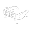
図14に、本実施形態における電子機器としてのHMDの外観を示す。
図15に、図14に示すHMDの光学的な構成の概要を示す。図15において、図14と同様の部分には同一符号を付し、適宜説明を省略する。
In FIG. 14, the external appearance of HMD as an electronic device in this embodiment is shown.
FIG. 15 shows an outline of the optical configuration of the HMD shown in FIG. In FIG. 15, the same parts as those in FIG.
本実施形態におけるHMD700は、テンプル710L,710Rと、ブリッジ720と、レンズ701L,701Rとを備えている。このHMD700は、図15に示すように、テンプル710L及びレンズ701Lの近傍に、左眼用の電気光学装置730L(又は電気光学装置730Lを備えた表示モジュール)及び光学レンズ702Lを備えている。また、HMD700は、図15に示すように、テンプル710R及びレンズ701Rの近傍に、右眼用の電気光学装置730R(又は電気光学装置730Rを備えた表示モジュール)及び光学レンズ702Rを備えている。
The
更に、HMD700は、図15に示すように、レンズ701Lからの光が左眼に届く光路上に配置されるハーフミラー703Lと、レンズ701Rからの光が右眼に届く光路上に配置されるハーフミラー703Rとを備えている。電気光学装置730L,730Rとして、それぞれ本実施形態の電気光学装置100を適用することができる。
Further, as shown in FIG. 15, the
電気光学装置730Lの画像表示面は、図15において右側を向くように配置され、電気光学装置730Lによる表示画像に対応した光は、光学レンズ702Lを介してハーフミラー703Lに照射される。ハーフミラー703Lは、光学レンズ702Lからの光を左眼が位置する方向に反射すると共に、レンズ701Lからの光を左眼が位置する方向に透過させる。
電気光学装置730Rの画像表示面は、図15において左側を向くように配置され、電気光学装置730Rによる表示画像に対応した光は、光学レンズ702Rを介してハーフミラー703Rに照射される。ハーフミラー703Rは、光学レンズ702Rからの光を右眼が位置する方向に反射すると共に、レンズ701Rからの光を右眼が位置する方向に透過させる。
The image display surface of the electro-
The image display surface of the electro-
これにより、HMD700の装着者は、電気光学装置730L,730Rの表示画像を、レンズ701L,702Rを介して入ってくる外の様子を重ね合わせたシースルー状態で観察することができる。
このとき、HMD700において、視差を伴う両眼画像のうち左眼用画像を電気光学装置730Lに表示させ、該両眼画像のうち右眼用画像を電気光学装置730Rに表示させることで、装着者は、立体感を有する画像を認識することができる。
As a result, the wearer of the
At this time, in the
以上のようなHMD700に本実施形態における電気光学装置100を適用することにより、静電破壊対策を十分に実施する一方で、より高画質の画像表示が可能となる。
By applying the electro-
以上、本発明に係る電気光学装置、及び電子機器等を上記の実施形態に基づいて説明したが、本発明は上記の実施形態に限定されるものではない。例えば、その要旨を逸脱しない範囲において種々の態様において実施することが可能であり、次のような変形も可能である。 The electro-optical device, the electronic apparatus, and the like according to the present invention have been described based on the above embodiment, but the present invention is not limited to the above embodiment. For example, the present invention can be implemented in various modes without departing from the gist thereof, and the following modifications are possible.
(1)本実施形態では、電気光学装置100が、図1に示す構成を例に説明したが、本発明は、これに限定されるものではない。
(1) In the present embodiment, the electro-
(2)本実施形態では、電気光学装置100の回路配置や電極配置が、図2や図4に示す配置であるものとして説明したが、本発明は、これらに限定されるものではない。
(2) In the present embodiment, the circuit arrangement and the electrode arrangement of the electro-
(3)本実施形態では、画素回路210の構成を図3に示す構成を例に説明したが、本発明は、これに限定されるものではない。
(3) In the present embodiment, the configuration of the
(4)本実施形態では、画素回路210内を構成するトランジスターがP型のMOSトランジスターであるものとして説明したが、本発明は、これに限定されるものではなく、少なくとも1つがN型のMOSトランジスターであってもよい。
(4) In the present embodiment, the transistor constituting the
(5)本実施形態では、電気光学装置100が適用された電子機器として、HMDを例に説明したが、本発明は、これに限定されるものではない。例えば、本発明に係る電子機器として、超小型ディスプレイとしてEVF等の直視型の表示パネルを用いた機器であってもよい。
また、本発明に係る電子機器として、情報携帯端末(PDA:Personal Digital Assistants)、デジタルスチルカメラ、テレビ、ビデオカメラ、カーナビゲーション装置、ページャー、電子手帳、電子ペーパー、電卓、ワードプロセッサー、ワークステーション、テレビ電話、POS(Point of sale system)端末、プリンター、スキャナー、複写機、ビデオプレーヤー、タッチパネルを備えた機器等が挙げられる。
(5) In this embodiment, the HMD is described as an example of the electronic apparatus to which the electro-
In addition, as an electronic device according to the present invention, a personal digital assistant (PDA), a digital still camera, a television, a video camera, a car navigation device, a pager, an electronic notebook, electronic paper, a calculator, a word processor, a workstation, a television Examples include telephones, point-of-sale (POS) terminals, printers, scanners, copiers, video players, and devices equipped with touch panels.
(6)上記の実施形態において、本発明を電気光学装置、及び電子機器等として説明したが、本発明は、これに限定されるものではない。例えば、本発明に係る電気光学装置の素子保護方法等であってもよい。 (6) In the above embodiments, the present invention has been described as an electro-optical device, an electronic apparatus, and the like, but the present invention is not limited to this. For example, an element protection method for an electro-optical device according to the present invention may be used.
10,100,100a,100b,100c,100d,730L,730R…電気光学装置、 12,200…表示部、 14,14a,14b,300…パッド、
16a…静電気保護回路、 18…配線、
110,110a,110b…走査線駆動回路、 120…データ線駆動回路、
130…テスト回路、 150…制御回路、 160…電源回路、 210…画素回路、
211〜214…トランジスター、 215…OLED、 216…保持容量、
250…VEL電極(第2の電極)、 260,260a,260b1,260b2,260c,260d1,260d2…VCT電極(第1の電極)、
310,330…保護回路、 312…保護素子(第1の保護素子)、
314…保護素子(第2の保護素子)、 316…保護抵抗、 320…実装用パッド、
400,410…接続配線、 500…P型半導体基板、
502,504…N型不純物領域、 506,508,510…P型不純物領域、
512,516…N型高濃度不純物領域、 514…P型高濃度不純物領域、
518,520…P型アクティブ領域、 600…表示モジュール、
610…FPC基板、 620…集積回路装置、 622…端子、
700…HMD、 701L,701R…レンズ、 702L,702R…光学レンズ、
703L,703R…ハーフミラー、 710L,710R…テンプル、
720…ブリッジ
10, 100, 100a, 100b, 100c, 100d, 730L, 730R ... electro-optical device, 12, 200 ... display unit, 14, 14a, 14b, 300 ... pad,
16a ... Electrostatic protection circuit, 18 ... Wiring,
110, 110a, 110b ... scanning line driving circuit, 120 ... data line driving circuit,
130 ...
211-214 ... transistor, 215 ... OLED, 216 ... retention capacity,
250 ... VEL electrode (second electrode), 260,260a, 260b 1, 260b 2, 260c,
310, 330 ... protection circuit, 312 ... protection element (first protection element),
314 ... Protection element (second protection element), 316 ... Protection resistance, 320 ... Mounting pad,
400, 410 ... connection wiring, 500 ... P-type semiconductor substrate,
502, 504 ... N-type impurity region, 506, 508, 510 ... P-type impurity region,
512, 516 ... N-type high concentration impurity region, 514 ... P-type high concentration impurity region,
518, 520 ... P-type active region, 600 ... Display module,
610 ... FPC board, 620 ... integrated circuit device, 622 ... terminal,
700 ... HMD, 701L, 701R ... lens, 702L, 702R ... optical lens,
703L, 703R ... half mirror, 710L, 710R ... temple,
720 ... Bridge
Claims (12)
複数の有機発光ダイオードと、
前記複数の有機発光ダイオードを構成する各有機発光ダイオードのカソードに共通に電気的に接続される第1の電極と、
一端が前記パッドに電気的に接続され、他端が前記第1の電極に電気的に接続される第1の保護素子とを含むことを特徴とする電気光学装置。 Pad,
A plurality of organic light emitting diodes;
A first electrode electrically connected in common to the cathode of each organic light emitting diode constituting the plurality of organic light emitting diodes;
An electro-optical device comprising: a first protection element having one end electrically connected to the pad and the other end electrically connected to the first electrode.
保護ダイオード、オフトランジスター、及びサイリスターのうちのいずれかであることを特徴とする請求項1に記載の電気光学装置。 The first protection element is:
The electro-optical device according to claim 1, wherein the electro-optical device is any one of a protective diode, an off-transistor, and a thyristor.
前記複数の駆動トランジスターを構成する各駆動トランジスターのソースに共通に電気的に接続される第2の電極と、
一端が前記パッドに電気的に接続され、他端が前記第2の電極に電気的に接続される第2の保護素子とを含むことを特徴とする請求項1又は2に記載の電気光学装置。 A plurality of driving transistors each supplying current to each of the organic light emitting diodes;
A second electrode that is electrically connected in common to the sources of the drive transistors constituting the plurality of drive transistors;
The electro-optical device according to claim 1, further comprising: a second protection element having one end electrically connected to the pad and the other end electrically connected to the second electrode. .
保護ダイオード、又はオフトランジスターであることを特徴とする請求項3に記載の電気光学装置。 The second protective element is:
The electro-optical device according to claim 3, wherein the electro-optical device is a protective diode or an off-transistor.
前記複数の有機発光ダイオードが形成される表示領域に平面視で重なるように配置され、
前記第1の電極は、
前記第2の電極を周回するように配置される1又は複数の電極により構成されることを特徴とする請求項3又は4に記載の電気光学装置。 The second electrode is
Arranged so as to overlap the display area in which the plurality of organic light emitting diodes are formed in plan view,
The first electrode is
The electro-optical device according to claim 3, wherein the electro-optical device includes one or a plurality of electrodes arranged so as to go around the second electrode.
前記複数の有機発光ダイオードが形成される表示領域に平面視で重なるように配置され、
前記第1の電極は、
前記第2の電極の外周辺のうち互いに交差する2辺に沿った外周辺を有することを特徴とする請求項3又は4に記載の電気光学装置。 The second electrode is
Arranged so as to overlap the display area in which the plurality of organic light emitting diodes are formed in plan view,
The first electrode is
5. The electro-optical device according to claim 3, further comprising an outer periphery along two sides that intersect each other among the outer periphery of the second electrode.
前記接続配線は、
前記第1の電極と平面視で重なるように配置されることを特徴とする請求項3乃至6のいずれか1項に記載の電気光学装置。 Including a connection wiring for electrically connecting the second electrode and the other end of the second protection element;
The connection wiring is
The electro-optical device according to claim 3, wherein the electro-optical device is disposed so as to overlap the first electrode in plan view.
前記第1の電極と前記第1の保護素子とを接続する配線のインピーダンスと前記第1の電極のインピーダンスとの合成インピーダンスが、前記電源パッドに電気的に接続される配線のインピーダンスより低いことを特徴とする請求項1乃至7のいずれか1項に記載の電気光学装置。 Including a power pad to which a ground voltage is supplied;
The combined impedance of the impedance of the wiring connecting the first electrode and the first protection element and the impedance of the first electrode is lower than the impedance of the wiring electrically connected to the power supply pad. The electro-optical device according to claim 1, wherein the electro-optical device is characterized in that:
前記電気光学装置が形成される基板の外周辺に沿って配置される複数のパッドの1つであることを特徴とする請求項1乃至8のいずれか1項に記載の電気光学装置。 The pad
9. The electro-optical device according to claim 1, wherein the electro-optical device is one of a plurality of pads arranged along an outer periphery of a substrate on which the electro-optical device is formed.
前記電気光学装置の実装用パッドであることを特徴とする請求項1乃至10のいずれか1項に記載の電気光学装置。 The pad
The electro-optical device according to claim 1, wherein the electro-optical device is a mounting pad for the electro-optical device.
Priority Applications (3)
| Application Number | Priority Date | Filing Date | Title |
|---|---|---|---|
| JP2013061550A JP2014186200A (en) | 2013-03-25 | 2013-03-25 | Electro-optic device and electronic apparatus |
| US14/196,849 US20140284571A1 (en) | 2013-03-25 | 2014-03-04 | Electrooptical device and electronic apparatus |
| CN201410111722.4A CN104078002A (en) | 2013-03-25 | 2014-03-24 | Electro-optic devices and electronics |
Applications Claiming Priority (1)
| Application Number | Priority Date | Filing Date | Title |
|---|---|---|---|
| JP2013061550A JP2014186200A (en) | 2013-03-25 | 2013-03-25 | Electro-optic device and electronic apparatus |
Publications (1)
| Publication Number | Publication Date |
|---|---|
| JP2014186200A true JP2014186200A (en) | 2014-10-02 |
Family
ID=51568467
Family Applications (1)
| Application Number | Title | Priority Date | Filing Date |
|---|---|---|---|
| JP2013061550A Pending JP2014186200A (en) | 2013-03-25 | 2013-03-25 | Electro-optic device and electronic apparatus |
Country Status (3)
| Country | Link |
|---|---|
| US (1) | US20140284571A1 (en) |
| JP (1) | JP2014186200A (en) |
| CN (1) | CN104078002A (en) |
Cited By (1)
| Publication number | Priority date | Publication date | Assignee | Title |
|---|---|---|---|---|
| JP2023527096A (en) * | 2020-03-17 | 2023-06-27 | 京東方科技集團股▲ふん▼有限公司 | Light-emitting substrate, driving method thereof, and display device |
Families Citing this family (6)
| Publication number | Priority date | Publication date | Assignee | Title |
|---|---|---|---|---|
| KR101747268B1 (en) * | 2015-11-30 | 2017-06-14 | 엘지디스플레이 주식회사 | Organic light emitting display device and head mounted display including the same |
| CN113809137A (en) | 2016-09-21 | 2021-12-17 | 索尼半导体解决方案公司 | Display device and electronic apparatus |
| CN107705742A (en) * | 2017-09-28 | 2018-02-16 | 惠科股份有限公司 | Display panel's drive circuit and display device |
| CN107993579B (en) * | 2017-11-29 | 2019-11-12 | 武汉天马微电子有限公司 | Display panel, driving method thereof and display device |
| US10948976B1 (en) * | 2019-02-06 | 2021-03-16 | Facebook Technologies, Llc | Systems and methods for electric discharge-based sensing via wearables donned by users of artificial reality systems |
| US11992102B2 (en) * | 2021-04-09 | 2024-05-28 | Samsung Electronics Co., Ltd. | Case for electronic device |
Family Cites Families (5)
| Publication number | Priority date | Publication date | Assignee | Title |
|---|---|---|---|---|
| JP3290772B2 (en) * | 1993-08-18 | 2002-06-10 | 株式会社東芝 | Display device |
| JP2006066871A (en) * | 2004-07-27 | 2006-03-09 | Seiko Epson Corp | LIGHT EMITTING DEVICE, IMAGE FORMING DEVICE, AND DISPLAY DEVICE |
| KR101574210B1 (en) * | 2008-09-25 | 2015-12-07 | 삼성디스플레이 주식회사 | Organic light emitting display and fabrication method of the same |
| KR101040859B1 (en) * | 2009-09-02 | 2011-06-14 | 삼성모바일디스플레이주식회사 | Organic light emitting display |
| KR102295450B1 (en) * | 2009-10-09 | 2021-08-27 | 가부시키가이샤 한도오따이 에네루기 켄큐쇼 | Display device |
-
2013
- 2013-03-25 JP JP2013061550A patent/JP2014186200A/en active Pending
-
2014
- 2014-03-04 US US14/196,849 patent/US20140284571A1/en not_active Abandoned
- 2014-03-24 CN CN201410111722.4A patent/CN104078002A/en active Pending
Cited By (2)
| Publication number | Priority date | Publication date | Assignee | Title |
|---|---|---|---|---|
| JP2023527096A (en) * | 2020-03-17 | 2023-06-27 | 京東方科技集團股▲ふん▼有限公司 | Light-emitting substrate, driving method thereof, and display device |
| JP7701275B2 (en) | 2020-03-17 | 2025-07-01 | 京東方科技集團股▲ふん▼有限公司 | Light-emitting substrate, driving method thereof, and display device |
Also Published As
| Publication number | Publication date |
|---|---|
| CN104078002A (en) | 2014-10-01 |
| US20140284571A1 (en) | 2014-09-25 |
Similar Documents
| Publication | Publication Date | Title |
|---|---|---|
| KR102051357B1 (en) | Electro-optical device and electronic apparatus | |
| JP6015095B2 (en) | Electro-optical device and electronic apparatus | |
| KR102048253B1 (en) | Electro-optical device and electronic apparatus | |
| US20190156762A1 (en) | Display device, electronic device, and driving method of display device | |
| JP5929136B2 (en) | Electro-optical device and electronic apparatus | |
| JP2014186200A (en) | Electro-optic device and electronic apparatus | |
| US12062341B2 (en) | Light-emitting device and electronic apparatus | |
| US11107406B2 (en) | Light-emitting device and electronic apparatus | |
| JP5929121B2 (en) | Electro-optical device and electronic apparatus | |
| KR20210065096A (en) | Display device and manufacturing method thereof | |
| JP6213644B2 (en) | Electro-optical device and electronic apparatus | |
| KR20200009008A (en) | Display device and electronic device | |
| US11132950B2 (en) | Electro-optical device and electronic apparatus | |
| US20250031535A1 (en) | Display device and mobile electronic device including the same | |
| JP2013238723A (en) | Electro-optic device and electronic apparatus | |
| US12586526B2 (en) | Display device and mobile electronic device including the same | |
| JP6673406B2 (en) | Electro-optical devices and electronic equipment | |
| JP6376258B2 (en) | Electro-optical device and electronic apparatus |
Legal Events
| Date | Code | Title | Description |
|---|---|---|---|
| RD04 | Notification of resignation of power of attorney |
Free format text: JAPANESE INTERMEDIATE CODE: A7424 Effective date: 20150109 |