CN102176444B - High integration level system in package (SIP) structure - Google Patents

High integration level system in package (SIP) structure Download PDF

Info

Publication number
CN102176444B
CN102176444B CN2011100696669A CN201110069666A CN102176444B CN 102176444 B CN102176444 B CN 102176444B CN 2011100696669 A CN2011100696669 A CN 2011100696669A CN 201110069666 A CN201110069666 A CN 201110069666A CN 102176444 B CN102176444 B CN 102176444B
Authority
CN
China
Prior art keywords
layer
wiring
substrate
packaging
chip
Prior art date
Legal status (The legal status is an assumption and is not a legal conclusion. Google has not performed a legal analysis and makes no representation as to the accuracy of the status listed.)
Active
Application number
CN2011100696669A
Other languages
Chinese (zh)
Other versions
CN102176444A (en
Inventor
陶玉娟
石磊
Current Assignee (The listed assignees may be inaccurate. Google has not performed a legal analysis and makes no representation or warranty as to the accuracy of the list.)
Tongfu Microelectronics Co Ltd
Original Assignee
Nantong Fujitsu Microelectronics Co Ltd
Priority date (The priority date is an assumption and is not a legal conclusion. Google has not performed a legal analysis and makes no representation as to the accuracy of the date listed.)
Filing date
Publication date
Application filed by Nantong Fujitsu Microelectronics Co Ltd filed Critical Nantong Fujitsu Microelectronics Co Ltd
Priority to CN2011100696669A priority Critical patent/CN102176444B/en
Publication of CN102176444A publication Critical patent/CN102176444A/en
Priority to PCT/CN2012/072769 priority patent/WO2012126377A1/en
Application granted granted Critical
Publication of CN102176444B publication Critical patent/CN102176444B/en
Priority to US15/362,625 priority patent/US10741499B2/en
Active legal-status Critical Current
Anticipated expiration legal-status Critical

Links

Images

Classifications

    • HELECTRICITY
    • H10SEMICONDUCTOR DEVICES; ELECTRIC SOLID-STATE DEVICES NOT OTHERWISE PROVIDED FOR
    • H10WGENERIC PACKAGES, INTERCONNECTIONS, CONNECTORS OR OTHER CONSTRUCTIONAL DETAILS OF DEVICES COVERED BY CLASS H10
    • H10W70/00Package substrates; Interposers; Redistribution layers [RDL]
    • H10W70/60Insulating or insulated package substrates; Interposers; Redistribution layers
    • HELECTRICITY
    • H10SEMICONDUCTOR DEVICES; ELECTRIC SOLID-STATE DEVICES NOT OTHERWISE PROVIDED FOR
    • H10WGENERIC PACKAGES, INTERCONNECTIONS, CONNECTORS OR OTHER CONSTRUCTIONAL DETAILS OF DEVICES COVERED BY CLASS H10
    • H10W72/00Interconnections or connectors in packages
    • H10W72/20Bump connectors, e.g. solder bumps or copper pillars; Dummy bumps; Thermal bumps
    • H10W72/241Dispositions, e.g. layouts
    • HELECTRICITY
    • H10SEMICONDUCTOR DEVICES; ELECTRIC SOLID-STATE DEVICES NOT OTHERWISE PROVIDED FOR
    • H10WGENERIC PACKAGES, INTERCONNECTIONS, CONNECTORS OR OTHER CONSTRUCTIONAL DETAILS OF DEVICES COVERED BY CLASS H10
    • H10W72/00Interconnections or connectors in packages
    • H10W72/851Dispositions of multiple connectors or interconnections
    • H10W72/874On different surfaces
    • HELECTRICITY
    • H10SEMICONDUCTOR DEVICES; ELECTRIC SOLID-STATE DEVICES NOT OTHERWISE PROVIDED FOR
    • H10WGENERIC PACKAGES, INTERCONNECTIONS, CONNECTORS OR OTHER CONSTRUCTIONAL DETAILS OF DEVICES COVERED BY CLASS H10
    • H10W74/00Encapsulations, e.g. protective coatings
    • HELECTRICITY
    • H10SEMICONDUCTOR DEVICES; ELECTRIC SOLID-STATE DEVICES NOT OTHERWISE PROVIDED FOR
    • H10WGENERIC PACKAGES, INTERCONNECTIONS, CONNECTORS OR OTHER CONSTRUCTIONAL DETAILS OF DEVICES COVERED BY CLASS H10
    • H10W74/00Encapsulations, e.g. protective coatings
    • H10W74/10Encapsulations, e.g. protective coatings characterised by their shape or disposition
    • H10W74/15Encapsulations, e.g. protective coatings characterised by their shape or disposition on active surfaces of flip-chip devices, e.g. underfills
    • HELECTRICITY
    • H10SEMICONDUCTOR DEVICES; ELECTRIC SOLID-STATE DEVICES NOT OTHERWISE PROVIDED FOR
    • H10WGENERIC PACKAGES, INTERCONNECTIONS, CONNECTORS OR OTHER CONSTRUCTIONAL DETAILS OF DEVICES COVERED BY CLASS H10
    • H10W90/00Package configurations
    • HELECTRICITY
    • H10SEMICONDUCTOR DEVICES; ELECTRIC SOLID-STATE DEVICES NOT OTHERWISE PROVIDED FOR
    • H10WGENERIC PACKAGES, INTERCONNECTIONS, CONNECTORS OR OTHER CONSTRUCTIONAL DETAILS OF DEVICES COVERED BY CLASS H10
    • H10W90/00Package configurations
    • H10W90/701Package configurations characterised by the relative positions of pads or connectors relative to package parts
    • H10W90/721Package configurations characterised by the relative positions of pads or connectors relative to package parts of bump connectors
    • H10W90/724Package configurations characterised by the relative positions of pads or connectors relative to package parts of bump connectors between a chip and a stacked insulating package substrate, interposer or RDL

Landscapes

  • Wire Bonding (AREA)

Abstract

本发明涉及高集成度系统级封装结构,包括基板;位于基板上的至少一组布线封装层,所述布线封装层包括依次位于基板上的正贴装层、封料层、布线层;位于布线封装层上的顶部倒装封装层,所述顶部倒装封装层包括依次位于布线封装层上的倒贴装层、底部填充料、封料层;设置于基板下方的连接球;其中,封装层之间透过布线层实现相邻封装层或间隔封装层间的电互联。与现有技术相比,本发明请求保护的高集成度系统级封装结构,可以形成包含整体系统功能而非单一的芯片功能的最终封装产品,降低了系统内电阻、电感以及芯片间的干扰因素。此外,可以形成更为复杂的多层互联结构,实现集成度更高的圆片系统级封装。

Figure 201110069666

The invention relates to a highly integrated system-level packaging structure, which includes a substrate; at least one group of wiring packaging layers located on the substrate, and the wiring packaging layer includes a positive mounting layer, a sealing material layer, and a wiring layer sequentially located on the substrate; The top flip-chip packaging layer on the packaging layer, the top flip-chip packaging layer includes a flip-chip packaging layer, an underfill material, and a sealing material layer sequentially located on the wiring packaging layer; connecting balls arranged under the substrate; wherein, the packaging layer The electrical interconnection between adjacent packaging layers or interval packaging layers is realized through the wiring layer. Compared with the prior art, the highly integrated system-in-package structure claimed in the present invention can form a final packaged product that includes the overall system function rather than a single chip function, reducing the internal resistance, inductance and interference factors between chips in the system . In addition, a more complex multi-layer interconnection structure can be formed to realize a system-in-a-wafer package with a higher degree of integration.

Figure 201110069666

Description

High-integration system-in-package structure
Technical Field
The present invention relates to semiconductor technologies, and in particular, to a high-integration system-in-package structure.
Background
With the continuous development of integrated circuit technology, electronic products are increasingly developing toward miniaturization, intellectualization, high performance and high reliability. The integrated circuit package not only directly affects the performance of the integrated circuit, the electronic module and even the complete machine, but also restricts the miniaturization, low cost and reliability of the whole electronic system. Under the conditions of the gradual reduction of the size of the integrated circuit wafer and the continuous improvement of the integration level, the electronic industry puts higher and higher requirements on the integrated circuit packaging technology.
A package substrate is disclosed in chinese patent No. CN 1747156C. The package substrate includes: a substrate, the substrate comprising a surface; the ball receiving pad is positioned on the surface of the substrate; the solder mask layer is formed on the surface of the substrate and comprises at least one opening, and the ball receiving pad is exposed out of the opening; the packaging substrate further comprises a patterned metal reinforcing layer, and the patterned metal reinforcing layer is formed on the ball pad along the side wall of the solder mask layer opening.
However, with the trend of light, thin, short and small semiconductor products and the increasing demand for system functions of products, how to further improve the integration of system-in-package is a problem to be solved by those skilled in the art.
Disclosure of Invention
The technical problem solved by the invention is as follows: how to realize a high-density system-in-package having a multi-layer structure.
To solve the above technical problem, the present invention provides a high-integration system-in-package structure, which includes: a substrate; the wiring packaging layer comprises a positive mounting layer, a material sealing layer and a wiring layer which are sequentially arranged on the substrate; the top flip-chip packaging layer is positioned on the wiring packaging layer and comprises a flip-chip packaging layer, a bottom filling material and a material sealing layer which are sequentially positioned on the wiring packaging layer; a connection ball disposed below the substrate; and the packaging layers are electrically interconnected through the wiring layer.
Optionally, the high-integration-level system-in-package structure includes a first wiring package layer, where the first wiring package layer includes a first front-mounting layer, a first material sealing layer, and a first wiring layer, which are sequentially located on the substrate.
Optionally, the functional side of each device in the first positive mounting layer faces upward.
Optionally, the first sealing material layer is filled between the devices of the first front mounting layer, and exposes the connecting members of the devices of the first front mounting layer.
Optionally, the wiring layer includes a longitudinal wiring penetrating through the sealing material layer, and a transverse wiring covering the sealing material layer and connected to the longitudinal wiring.
Optionally, the functional side of each device in the flip-chip layer faces downward.
Optionally, the sealing material layer of the top flip-chip packaging layer is filled between the devices of the flip-chip packaging layer and encapsulates the flip-chip packaging layer.
Optionally, the substrate is a BT substrate or a PCB substrate.
Optionally, the front mounting layer includes a single chip or multiple chips, and the back mounting layer includes a single chip or multiple chips.
Optionally, the front mounting layer further includes a passive device, and the passive device of the front mounting layer is one or more of a capacitor, a resistor, or an inductor.
Compared with the prior art, the high-integration-level system-in-package structure disclosed by the invention integrates the chip and the passive device and then packages the integrated chip and the passive device together, so that a final package product comprising the functions of the whole system instead of a single chip can be formed; meanwhile, the interconnection of a high-density system in a three-dimensional angle is realized through the wiring layers among the multilayer packaging layers, compared with the existing system-in-package, the multilayer wiring structure fully utilizes the thickness of the chip, meets the trend requirement of light, thin, short and small semiconductor packaging and the more complex system function integration requirement, and simultaneously better reduces the resistance, inductance and interference factors among the chips in the system, and the structural strength and the product reliability are well enhanced.
Drawings
Fig. 1 is a schematic diagram of an embodiment of a high-integration system-in-package structure according to the present invention.
Detailed Description
In the following description, numerous specific details are set forth in order to provide a thorough understanding of the present invention. This invention may, however, be embodied in many different forms and should not be construed as limited to the embodiments set forth herein, but rather construed as limited to the embodiments set forth herein.
Next, the present invention is described in detail by using schematic diagrams, and when the embodiments of the present invention are described in detail, the schematic diagrams are only examples for convenience of description, and the scope of the present invention should not be limited herein.
The invention provides a high-integration level system-in-package structure, which comprises: a substrate; the wiring packaging layer comprises a positive mounting layer, a material sealing layer and a wiring layer which are sequentially arranged on the substrate; the top flip-chip packaging layer is positioned on the wiring packaging layer and comprises a flip-chip packaging layer, bottom filling and a material sealing layer which are sequentially positioned on the wiring packaging layer; a connection ball disposed below the substrate; and the packaging layers are electrically interconnected through the wiring layer.
The following detailed description of embodiments of the invention refers to the accompanying drawings.
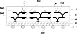
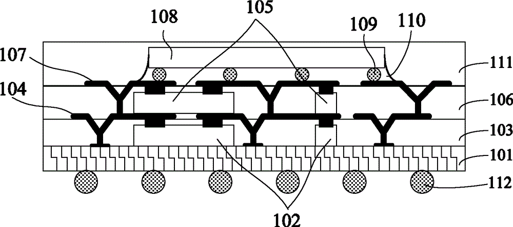
Referring to fig. 1, a schematic diagram of an embodiment of a high-integration system-in-package structure according to the present invention is shown, in this embodiment, two sets of a wiring package layer and a top flip-chip package layer are taken as an example of the high-integration system-in-package structure, but the present invention is not limited thereto, and the high-integration system-in-package structure includes: the package structure comprises a substrate 101, a first wiring packaging layer positioned on the substrate 101, a second wiring packaging layer positioned on the first wiring packaging layer, a top flip-chip packaging layer positioned on the second wiring packaging layer, and connecting balls 110 arranged below the substrate 101. Wherein,
the substrate 101 is a base for subsequently stacking each package group and also a base for carrying subsequent layers of package layers. The substrate 101 includes two functional surfaces, wherein a first surface of the substrate 101 is used for stacking a package layer, and a second surface of the substrate 101 is used for embedding balls (embedding connection balls), in this embodiment, an upper surface of the substrate 101 is used for stacking a package layer, the upper surface of the substrate 101 is provided with a pad for realizing electrical connection, and a lower surface of the substrate 101 is used for embedding connection balls. Specifically, the substrate 101 is typically a bt (bimoleimide) substrate or a Printed Circuit Board (PCB), etc., so as to facilitate routing between the first surface and the second surface of the substrate 101. The substrate 101 includes a connection trace penetrating through the substrate 101, and the connection trace can electrically connect the pad and the connection ball.
In order to fix the package on the substrate 101 better, the high-integration system-in-package structure further includes a glue layer attached to the substrate 101, the glue layer is used to attach the first mounting layer 103 to the substrate 101, the glue layer may be made of various materials, and the glue layer formed on the substrate 101 may be dispensed or printed. Such methods are well known to those skilled in the art of semiconductor fabrication and will not be described in detail herein.
The first wiring encapsulation layer comprises a first positive mounting layer 102, a first material sealing layer 103 and a first wiring layer 104 which are sequentially arranged on the substrate 101. Wherein,
the first front mounting layer 102 includes a plurality of semiconductor devices, in this embodiment, the first front mounting layer 102 includes a chip and a passive device, and is attached to the substrate 101 through a glue layer in a manner that a functional surface faces upward, where the functional surface of the first front mounting layer 102 refers to a surface where pads of the chip and the passive device in the first front mounting layer 102 are located.
In a preferred embodiment of the present invention, the first positive mounting layer 102 and the subsequent-mentioned mounting layers disposed on the substrate 101 may comprise one or more same or different chips, and may further comprise one or more same or different passive devices. These chips and passive devices each become part of a system-in-package product, each performing one or more individual functions among the system-in-package functions.
In a preferred embodiment of the present invention, the combination of the chip and the passive device in the first positive mounting layer 102 is configured according to the system function. Therefore, around one or a group of chips, there may be another chip or group of chips, which may be the same or different, or passive devices such as capacitors, resistors or inductors, which may be the same or different; similarly, there may be other passive devices that are the same or different, or one or more of the same or different chips, around a passive device.
The first encapsulant layer 103 serves to insulate and isolate the various devices of the first front side mounting layer 102, as well as to insulate and isolate the different encapsulation layers. The first sealing material layer 103 is filled between the devices of the first front mounting layer 102, and a part of the first sealing material layer 103 covers the devices of the first front mounting layer 102, the first sealing material layer 103 exposes the connectors of the devices of the first front mounting layer 102, and specifically, the first sealing material layer 103 exposes the surfaces of the bonding pads of the chip and the passive device group, so as to facilitate electrical connection.
Since the first sealing material layer 103 is filled between the devices of the first front mounting layer 102 and exposes the connectors of the devices, the thickness of the first sealing material layer 103 is equal to that of the first front mounting layer 102, so that the stacking thickness of the mounting layers can be reduced, and the integration of the package structure can be improved to the maximum extent.
The first wiring layer 104 includes a first vertical wiring and a first horizontal wiring. The first longitudinal wiring is a wire (e.g., a metal wire) penetrating through the first encapsulant layer 103, and is used for electrically connecting the first wiring encapsulation layer and the substrate 101.
In practical application, longitudinal wiring can be selectively formed in the sealing material layer according to design requirements so as to realize the electrical connection between the mounting layers or between the mounting layers and the substrate.
The first transverse wiring is a wire (e.g., a metal wire) covering the first encapsulant layer 103 and is conductively connected to the first longitudinal wiring for electrically connecting the devices of the first front mounting layer 102, in this embodiment, the first transverse wiring is used for electrically connecting the chip and the passive device group in the first front mounting layer 102, and specifically, the first transverse wiring is connected to the pad surfaces of the chip and the passive device.
The second wiring encapsulation layer is stacked on the first wiring encapsulation layer, and specifically comprises: and the second positive mounting layer 105, the second material sealing layer 106 and the second wiring layer 107 are sequentially positioned on the first wiring packaging layer. In this embodiment, the second front mounting layer 105 includes a chip and a passive device, and is stacked on the first sealing material layer 103 in a manner that the functional surface faces upward. The second front mounting layer 105, similar to the first front mounting layer 102, may include one or more same or different chips, and may further include one or more same or different passive devices.
The second encapsulant layer 106 serves to insulate and isolate the individual devices of the second positive mounting layer 105, as well as to insulate and isolate the different encapsulation layers. The second sealing material layer 106 is filled between the devices of the second front mounting layer 105, and a part of the second sealing material layer 106 covers the devices of the second front mounting layer 105, the second sealing material layer 106 exposes the connectors of the devices of the second front mounting layer 106, and specifically, the second sealing material layer 106 exposes the surfaces of the bonding pads of the chip and the passive device group, so as to facilitate electrical connection.
The second wiring layer 107 includes a second vertical wiring and a second horizontal wiring. The second vertical wirings are wires (e.g., metal wires) penetrating through the second encapsulant layer 106, and are used for realizing electrical connection between the second wiring encapsulation layer and other encapsulation layers, and according to design requirements, the second vertical wirings are also used for realizing electrical connection between the second wiring encapsulation layer and the substrate 101;
the second transverse wiring is a wire (e.g., a metal wire) covering the second encapsulant layer 106, and the second transverse wiring is connected to the second longitudinal wiring for electrically connecting devices of the second front mounting layer 105, in this embodiment, the second transverse wiring is used for electrically connecting a chip and a passive device group in the second front mounting layer 105.
The top flip-chip package layer includes a flip-chip layer 108, an underfill, and a third encapsulant layer 111 sequentially on the second wire-bond package layer.
The flip-chip mounting layer 108, similar to the mounting layer described above, may contain one or more of the same or different chips and may also include one or more of the same or different passive devices. In this embodiment, the flip-chip layer 108 includes a chip and is attached to the second encapsulant layer 106 in a functional-surface-down manner, the functional surface of the chip has solder bumps 109, and the chip is electrically connected to the second transverse wires of the second wiring layer 107 through the solder bumps 109.
In a preferred embodiment of the present invention, passive devices may be disposed around the flip chip according to design requirements, and a mounting direction of the passive devices may be consistent with a mounting direction of the chip to simplify a process flow.
A filler 110 is disposed in a gap between the chip of the flip chip package 108 and the second wire encapsulation layer to form an underfill. The underfill is used for avoiding product reliability problems such as internal cavities in the sealant layer. The filler 110 may be a high molecular epoxy resin, which has good fluidity and can fully fill the gap between the flip chip and the encapsulant layer.
The third encapsulant layer 111 encapsulates the devices of the flip-chip packaging layer 108 to form a package body, so as to prevent pollution and corrosion of the external environment. The material forming the third encapsulant layer 111 may be the same as the material forming the first encapsulant layer 103 and the second encapsulant layer 106, i.e., epoxy is used to form the third encapsulant layer 111.
The high-integration system-in-package structure further includes a connection ball 112 disposed below the substrate 101, where the connection ball 112 is located at a position corresponding to the connection trace in the substrate 101, and is connected to the pad of the substrate 101 through the connection trace in the substrate 101.
The above embodiments include two wiring encapsulation layers and a top flip-chip encapsulation layer, but the present invention is not limited thereto, and one or more wiring encapsulation layers may be used to match with the top encapsulation layer, and those skilled in the art may make modifications, alterations and substitutions according to the above embodiments.
According to the high-integration system-level packaging structure, the electrical connection between adjacent or separated packaging layers is realized through the wiring layers, the integration of the system is realized through the arrangement of the connecting wires in the substrate 101, and finally the functions are output through the connecting balls 112.
Although the present invention has been described with reference to the preferred embodiments, it is not limited thereto. Various changes and modifications may be effected therein by one skilled in the art without departing from the spirit and scope of the invention as defined in the appended claims.

Claims (10)

1.高集成度系统级封装结构,其特征在于,包括:1. Highly integrated system-in-package structure, characterized in that it includes: 基板;位于基板上的至少一组布线封装层,所述布线封装层包括依次位于基板上的正贴装层、封料层、布线层;位于布线封装层上的顶部倒装封装层,所述顶部倒装封装层包括依次位于布线封装层上的倒贴装层、底部填充料、封料层;设置于基板下方的连接球;其中,封装层之间透过布线层实现相邻封装层或间隔封装层间的电互联。Substrate; at least one group of wiring encapsulation layers on the substrate, the wiring encapsulation layer includes a positive mounting layer, a sealing material layer, and a wiring layer sequentially located on the substrate; a top flip-chip encapsulation layer on the wiring encapsulation layer, the The top flip-chip packaging layer includes a flip-chip layer, an underfill material, and a sealing material layer sequentially located on the wiring packaging layer; connecting balls are arranged under the substrate; wherein, the wiring layer between the packaging layers realizes the adjacent packaging layer or interval Electrical interconnection between packaging layers. 2.如权利要求1所述的高集成度系统级封装结构,其特征在于,所述高集成度系统级封装结构包括第一布线封装层,所述第一布线封装层包括依次位于基板上的第一正贴装层、第一封料层、第一布线层。2. The highly integrated system-in-package structure according to claim 1, wherein the highly integrated system-in-package structure comprises a first wiring packaging layer, and the first wiring packaging layer comprises sequentially positioned on the substrate. The first positive mounting layer, the first packaging material layer, and the first wiring layer. 3.如权利要求2所述的高集成度系统级封装结构,其特征在于,所述第一正贴装层中各个器件的功能面朝上。3 . The highly integrated system-in-package structure according to claim 2 , wherein the functional faces of the devices in the first positive mounting layer face upward. 4 . 4.如权利要求2所述的高集成度系统级封装结构,其特征在于,所述第一封料层填充于第一正贴装层各个器件之间,并裸露出所述第一正贴装层各个器件的连接件。4. The highly integrated system-in-package structure according to claim 2, wherein the first encapsulant layer is filled between the devices of the first positive mounting layer and exposes the first positive mounting layer. Layer the connectors of each device. 5.如权利要求1所述的高集成度系统级封装结构,其特征在于,所述布线层包括贯穿所在封料层的纵向布线、覆盖于所在封料层上且连接于所述纵向布线的横向布线。5. The highly integrated system-in-package structure according to claim 1, wherein the wiring layer includes a vertical wiring penetrating through the encapsulant layer, a wire covering the encapsulant layer and connected to the vertical wiring. Horizontal wiring. 6.如权利要求1所述的高集成度系统级封装结构,其特征在于,所述倒贴装层中各个器件的功能面朝下。6 . The highly integrated system-in-package structure according to claim 1 , wherein the function of each device in the flip-mount layer faces downward. 7.如权利要求1所述的高集成度系统级封装结构,其特征在于,所述顶部倒装封装层的封料层填充于倒贴装层各个器件之间并将倒贴装层包覆密封。7 . The highly integrated system-in-package structure according to claim 1 , wherein the encapsulant layer of the top flip-chip packaging layer is filled between each device of the flip-chip layer and encapsulates and seals the flip-chip layer. 8.如权利要求1所述的高集成度系统级封装结构,其特征在于:所述基板为BT基板或PCB基板。8. The highly integrated system-in-package structure according to claim 1, wherein the substrate is a BT substrate or a PCB substrate. 9.如权利要求1~7任意一权利要求所述的高集成度系统级封装结构,其特征在于:所述正贴装层中包括单颗或多颗芯片,所述倒贴装层中包括单颗或多颗芯片。9. The highly integrated system-in-package structure according to any one of claims 1 to 7, wherein the front mounting layer includes a single chip or multiple chips, and the flip mounting layer includes a single chip one or more chips. 10.如权利要求9所述的高集成度系统级封装结构,其特征在于:所述正贴装层还包括无源器件,所述正贴装层的无源器件为电容、电阻或电感中的一种或多种。10. The highly integrated system-in-package structure according to claim 9, characterized in that: the positive mounting layer also includes passive devices, and the passive devices of the positive mounting layer are capacitors, resistors or inductors one or more of .
CN2011100696669A 2011-03-22 2011-03-22 High integration level system in package (SIP) structure Active CN102176444B (en)

Priority Applications (3)

Application Number Priority Date Filing Date Title
CN2011100696669A CN102176444B (en) 2011-03-22 2011-03-22 High integration level system in package (SIP) structure
PCT/CN2012/072769 WO2012126377A1 (en) 2011-03-22 2012-03-22 System-level packaging methods and structures
US15/362,625 US10741499B2 (en) 2011-03-22 2016-11-28 System-level packaging structures

Applications Claiming Priority (1)

Application Number Priority Date Filing Date Title
CN2011100696669A CN102176444B (en) 2011-03-22 2011-03-22 High integration level system in package (SIP) structure

Publications (2)

Publication Number Publication Date
CN102176444A CN102176444A (en) 2011-09-07
CN102176444B true CN102176444B (en) 2013-07-03

Family

ID=44519589

Family Applications (1)

Application Number Title Priority Date Filing Date
CN2011100696669A Active CN102176444B (en) 2011-03-22 2011-03-22 High integration level system in package (SIP) structure

Country Status (1)

Country Link
CN (1) CN102176444B (en)

Families Citing this family (7)

* Cited by examiner, † Cited by third party
Publication number Priority date Publication date Assignee Title
WO2012126377A1 (en) 2011-03-22 2012-09-27 Nantong Fujitsu Microelectronics Co., Ltd. System-level packaging methods and structures
US9543269B2 (en) 2011-03-22 2017-01-10 Nantong Fujitsu Microelectronics Co., Ltd. System-level packaging methods and structures
CN102157502B (en) * 2011-03-23 2014-05-07 南通富士通微电子股份有限公司 System-in-package structure
US9099448B2 (en) * 2011-03-23 2015-08-04 Nantong Fujitsu Microelectronics Co., Ltd. Three-dimensional system-level packaging methods and structures
CN105047657A (en) * 2015-08-13 2015-11-11 陈明涵 AIO packaged structure and packaging method
CN105552054B (en) * 2016-02-03 2018-02-27 美新半导体(无锡)有限公司 A kind of wafer level packaging structure and its manufacture method
CN113299620B (en) * 2021-05-21 2023-01-06 维沃移动通信有限公司 Packaging structure, circuit board assembly and electronic equipment

Citations (3)

* Cited by examiner, † Cited by third party
Publication number Priority date Publication date Assignee Title
CN100514633C (en) * 2006-09-12 2009-07-15 日月光半导体制造股份有限公司 System-in-package structure
CN101789420A (en) * 2010-02-03 2010-07-28 南通富士通微电子股份有限公司 System-in-a-package (SIP) structure of semiconductor device and manufacturing method thereof
CN202025746U (en) * 2011-03-22 2011-11-02 南通富士通微电子股份有限公司 High integrated level SiP structure

Family Cites Families (1)

* Cited by examiner, † Cited by third party
Publication number Priority date Publication date Assignee Title
US7989269B2 (en) * 2008-03-13 2011-08-02 Stats Chippac, Ltd. Semiconductor package with penetrable encapsulant joining semiconductor die and method thereof

Patent Citations (3)

* Cited by examiner, † Cited by third party
Publication number Priority date Publication date Assignee Title
CN100514633C (en) * 2006-09-12 2009-07-15 日月光半导体制造股份有限公司 System-in-package structure
CN101789420A (en) * 2010-02-03 2010-07-28 南通富士通微电子股份有限公司 System-in-a-package (SIP) structure of semiconductor device and manufacturing method thereof
CN202025746U (en) * 2011-03-22 2011-11-02 南通富士通微电子股份有限公司 High integrated level SiP structure

Also Published As

Publication number Publication date
CN102176444A (en) 2011-09-07

Similar Documents

Publication Publication Date Title
CN102867800B (en) Functional chip is connected to packaging part to form package on package
KR101190920B1 (en) Stacked semiconductor package and method of manufacturing thereof
US7888785B2 (en) Semiconductor package embedded in substrate, system including the same and associated methods
CN102176444B (en) High integration level system in package (SIP) structure
TWI416700B (en) Wafer stacked package structure and manufacturing method thereof
CN102176450B (en) High-density system-in-package structure
CN102157394A (en) High-density system-in-a-package method
CN202025746U (en) High integrated level SiP structure
US10741499B2 (en) System-level packaging structures
CN102157402B (en) System-in-package method
CN105957841A (en) Semiconductor packaging structure
CN201994292U (en) High-density system-level packaging structure
US10515883B2 (en) 3D system-level packaging methods and structures
CN102769009A (en) Semiconductor packaging piece
CN102176419B (en) Method of high-integrated-level SiP (system in package)
CN102176448B (en) Fanout system class encapsulation structure
CN102157502B (en) System-in-package structure
CN102176445B (en) Fan-out high-density packaging structure
CN102176446B (en) A kind of Three-dimensional high-integration system-in-package structure
CN102176449B (en) High-density system-in-package structure
CN102176420A (en) Three-dimensional high-density system in package (SIP) method
CN202025748U (en) High-density system-on-package structure
CN201994291U (en) Three-dimensional high-integration system-in-package structure
CN202025749U (en) Three-dimensional high-density system level packaging structure
CN201994290U (en) Fan-out high-density package structure

Legal Events

Date Code Title Description
C06 Publication
PB01 Publication
C10 Entry into substantive examination
SE01 Entry into force of request for substantive examination
C14 Grant of patent or utility model
GR01 Patent grant
C56 Change in the name or address of the patentee
CP01 Change in the name or title of a patent holder

Address after: 226006 Jiangsu Province, Nantong City Chongchuan District Chongchuan Road No. 288

Patentee after: Tongfu Microelectronics Co., Ltd.

Address before: 226006 Jiangsu Province, Nantong City Chongchuan District Chongchuan Road No. 288

Patentee before: Fujitsu Microelectronics Co., Ltd., Nantong