KR101627728B1 - 박막 트랜지스터 기판 및 그 제조 방법 - Google Patents
박막 트랜지스터 기판 및 그 제조 방법 Download PDFInfo
- Publication number
- KR101627728B1 KR101627728B1 KR1020080136895A KR20080136895A KR101627728B1 KR 101627728 B1 KR101627728 B1 KR 101627728B1 KR 1020080136895 A KR1020080136895 A KR 1020080136895A KR 20080136895 A KR20080136895 A KR 20080136895A KR 101627728 B1 KR101627728 B1 KR 101627728B1
- Authority
- KR
- South Korea
- Prior art keywords
- protective film
- layer
- forming
- gate
- etching
- Prior art date
- Legal status (The legal status is an assumption and is not a legal conclusion. Google has not performed a legal analysis and makes no representation as to the accuracy of the status listed.)
- Expired - Fee Related
Links
Images


Classifications
-
- H—ELECTRICITY
- H10—SEMICONDUCTOR DEVICES; ELECTRIC SOLID-STATE DEVICES NOT OTHERWISE PROVIDED FOR
- H10D—INORGANIC ELECTRIC SEMICONDUCTOR DEVICES
- H10D86/00—Integrated devices formed in or on insulating or conducting substrates, e.g. formed in silicon-on-insulator [SOI] substrates or on stainless steel or glass substrates
- H10D86/40—Integrated devices formed in or on insulating or conducting substrates, e.g. formed in silicon-on-insulator [SOI] substrates or on stainless steel or glass substrates characterised by multiple TFTs
-
- H—ELECTRICITY
- H10—SEMICONDUCTOR DEVICES; ELECTRIC SOLID-STATE DEVICES NOT OTHERWISE PROVIDED FOR
- H10D—INORGANIC ELECTRIC SEMICONDUCTOR DEVICES
- H10D30/00—Field-effect transistors [FET]
- H10D30/60—Insulated-gate field-effect transistors [IGFET]
- H10D30/67—Thin-film transistors [TFT]
- H10D30/674—Thin-film transistors [TFT] characterised by the active materials
- H10D30/6755—Oxide semiconductors, e.g. zinc oxide, copper aluminium oxide or cadmium stannate
-
- H—ELECTRICITY
- H10—SEMICONDUCTOR DEVICES; ELECTRIC SOLID-STATE DEVICES NOT OTHERWISE PROVIDED FOR
- H10D—INORGANIC ELECTRIC SEMICONDUCTOR DEVICES
- H10D86/00—Integrated devices formed in or on insulating or conducting substrates, e.g. formed in silicon-on-insulator [SOI] substrates or on stainless steel or glass substrates
- H10D86/01—Manufacture or treatment
- H10D86/021—Manufacture or treatment of multiple TFTs
- H10D86/0231—Manufacture or treatment of multiple TFTs using masks, e.g. half-tone masks
-
- H—ELECTRICITY
- H10—SEMICONDUCTOR DEVICES; ELECTRIC SOLID-STATE DEVICES NOT OTHERWISE PROVIDED FOR
- H10D—INORGANIC ELECTRIC SEMICONDUCTOR DEVICES
- H10D86/00—Integrated devices formed in or on insulating or conducting substrates, e.g. formed in silicon-on-insulator [SOI] substrates or on stainless steel or glass substrates
- H10D86/40—Integrated devices formed in or on insulating or conducting substrates, e.g. formed in silicon-on-insulator [SOI] substrates or on stainless steel or glass substrates characterised by multiple TFTs
- H10D86/421—Integrated devices formed in or on insulating or conducting substrates, e.g. formed in silicon-on-insulator [SOI] substrates or on stainless steel or glass substrates characterised by multiple TFTs having a particular composition, shape or crystalline structure of the active layer
- H10D86/423—Integrated devices formed in or on insulating or conducting substrates, e.g. formed in silicon-on-insulator [SOI] substrates or on stainless steel or glass substrates characterised by multiple TFTs having a particular composition, shape or crystalline structure of the active layer comprising semiconductor materials not belonging to the Group IV, e.g. InGaZnO
-
- H—ELECTRICITY
- H10—SEMICONDUCTOR DEVICES; ELECTRIC SOLID-STATE DEVICES NOT OTHERWISE PROVIDED FOR
- H10D—INORGANIC ELECTRIC SEMICONDUCTOR DEVICES
- H10D86/00—Integrated devices formed in or on insulating or conducting substrates, e.g. formed in silicon-on-insulator [SOI] substrates or on stainless steel or glass substrates
- H10D86/40—Integrated devices formed in or on insulating or conducting substrates, e.g. formed in silicon-on-insulator [SOI] substrates or on stainless steel or glass substrates characterised by multiple TFTs
- H10D86/451—Integrated devices formed in or on insulating or conducting substrates, e.g. formed in silicon-on-insulator [SOI] substrates or on stainless steel or glass substrates characterised by multiple TFTs characterised by the compositions or shapes of the interlayer dielectrics
-
- H—ELECTRICITY
- H10—SEMICONDUCTOR DEVICES; ELECTRIC SOLID-STATE DEVICES NOT OTHERWISE PROVIDED FOR
- H10D—INORGANIC ELECTRIC SEMICONDUCTOR DEVICES
- H10D86/00—Integrated devices formed in or on insulating or conducting substrates, e.g. formed in silicon-on-insulator [SOI] substrates or on stainless steel or glass substrates
- H10D86/40—Integrated devices formed in or on insulating or conducting substrates, e.g. formed in silicon-on-insulator [SOI] substrates or on stainless steel or glass substrates characterised by multiple TFTs
- H10D86/60—Integrated devices formed in or on insulating or conducting substrates, e.g. formed in silicon-on-insulator [SOI] substrates or on stainless steel or glass substrates characterised by multiple TFTs wherein the TFTs are in active matrices
Landscapes
- Thin Film Transistor (AREA)
Abstract
Description
Claims (17)
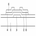
- 절연 기판 상에 게이트 라인 및 게이트 전극을 포함하는 게이트 배선을 형성하는 단계,상기 게이트 배선 상에 게이트 절연막을 형성하는 단계,상기 게이트 절연막 상에 반도체층과, 데이터 라인, 소오스 전극, 및 드레인 전극을 포함하는 데이터 배선을 형성하는 단계,상기 데이터 배선 상에 제 1 보호막을 형성하는 단계,제 1 온도 범위로 상기 제 1 보호막의 상부에 제 2 보호막을 형성하는 단계,제 1 온도 범위 보다 높은 제 2 온도 범위로 상기 제 2 보호막의 상부에 연속하여 제 3 보호막을 형성하는 단계,상기 제 3 보호막, 상기 제 2 보호막 및 상기 제 1 보호막을 연속 식각하여, 드레인 전극-화소 전극 콘택부의 드레인 전극을 노출하는 단계, 및상기 드레인 전극과 전기적으로 연결된 화소 전극을 형성하는 단계를 포함하는 박막 트랜지스터 어레이 기판의 제조 방법.
- 제 1항에 있어서, 상기 반도체층은 Hf, Zn, In, Ga, Sn 및 이들의 조합에서 선택된 물질의 산화물로 이루어진 박막 트랜지스터 어레이 기판의 제조 방법.
- 제 1항에 있어서, 상기 제 1 보호막, 상기 제 2 보호막 및 상기 제 3 보호막은 등방성 식각으로 진행되는 박막 트랜지스터 어레이 기판의 제조 방법.
- 제 3 항에 있어서, 상기 제 2 보호막은 상기 제 3 보호막보다 식각률이 높아 측면부에서 언더컷이 형성되는 박막트랜지스터 어레이 기판의 제조 방법.
- 제 1 항에 있어서, 상기 제 1 보호막은 산화규소 또는 산질화 규소를 포함하고, 상기 제 2 보호막과 상기 제 3 보호막은 질화규소를 포함하는 박막 트랜지스터 어레이 기판의 제조 방법.
- 제 3항에 있어서, 상기 제 3 보호막, 상기 제 2 보호막 및 상기 제 1 보호막을 식각하는 단계는상기 제 3 보호막 상부에 포토레지스트 층을 형성하는 단계,상기 포토레지스트 층을 노광 및 현상하여 패터닝하는 단계,패터닝된 상기 포토레지스트 층을 식각 마스크로 하여 상기 제 1, 제2, 제3 보호막을 식각하고,상기 제 2 보호막은 식각시에 상기 제 3 보호막보다 더 식각되어 측면에서 언더컷이 형성되는 단계를 포함하는박막 트랜지스터 어레이 기판의 제조 방법.
- 제 6항에 있어서, 상기 화소 전극을 형성하는 단계는식각 마스크로 이용된 상기 포토레지스트층을 제거하고 상기 제 3 보호막을 전면노출하는 단계,노출된 상기 제 3 보호막 상부에 화소 전극용 도전 물질을 적층하는 단계,PE 모드에서 상기 제 2 보호막 및 제 3 보호막을 식각하는 단계,상기 제 3 보호막 상부에 형성된 화소 전극용 도전 물질을 세정 공정을 통하여 제거하는 단계를 포함하는 박막 트랜지스터 어레이 기판의 제조 방법.
- 절연 기판 상에 게이트 라인 및 게이트 전극을 포함하는 게이트 배선을 형성하는 단계,상기 게이트 배선 상에 게이트 절연막을 형성하는 단계,상기 게이트 절연막 상에 반도체층과, 데이터 라인, 소오스 전극, 및 드레인 전극을 포함하는 데이터 배선을 형성하는 단계,상기 데이터 배선 상에 제 1 보호막을 형성하는 단계,상기 제 1 보호막 상부에 제 2 보호막을 형성하는 단계,상기 제 2 보호막 및 상기 제 1 보호막을 건식 식각 및 습식 식각하여, 드레인 전극-화소 전극 콘택부의 드레인 전극을 노출하는 단계 및 상기 드레인 전극과 전기적으로 연결된 화소 전극을 형성하는 단계를 포함하고,상기 제 2 보호막 및 상기 제 1 보호막을 습식 식각하는 단계는 상기 드레인 전극-화소 전극 콘택부에서 드러나는 상기 제 1 보호막의 측면을 과식각하여 상기 제 1 보호막의 언더컷을 형성하는 단계를 포함하는 박막 트랜지스터 어레이 기판의 제조 방법.
- 제 8항에 있어서, 상기 반도체층은 Hf, Zn, In, Ga, Sn 및 이들의 조합에서 선택된 물질의 산화물로 이루어진 박막 트랜지스터 어레이 기판의 제조 방법.
- 제 8항에 있어서, 상기 제 2 보호막 및 상기 제 1 보호막을 습식 식각하는 단계에서, HF를 포함하는 습식 식각액을 이용하는 박막 트랜지스터 어레이 기판의 제조 방법.
- 제 9항에 있어서, 상기 제 1 보호막은 산화규소 또는 산질화 규소를 포함하고, 상기 제 2 보호막은 질화규소를 포함하는 박막 트랜지스터 어레이 기판의 제조 방법.
- 제 8항에 있어서, 상기 제 1 보호막 및 상기 제 2 보호막을 식각하는 단계는상기 제 2 보호막 상부에 포토레지스트 층을 형성하는 단계상기 포토레지스트 층을 노광 및 현상하여 패터닝하는 단계패터닝된 상기 포토레지스트 층을 식각 마스크로 하여 상기 제1 및 제2 보호막을 식각하고, 상기 제 1 보호막은 상기 제 2 보호막보다 더 식각되어 측면에서 언더컷이 형성되는 단계를 포함하는 박막 트랜지스터 어레이 기판의 제조 방법.
- 제 12항에 있어서, 상기 화소 전극을 형성하는 단계는,식각 마스크로 이용된 상기 포토레지스트층을 제거하고 상기 제 2 보호막을 전면 노출하는 단계,상기 노출된 제 2 보호막 상부에 화소 전극용 도전 물질을 적층하는 단계,PE 모드에서 상기 제 2 보호막을 식각하는 단계, 및상기 제 2 보호막 상부에 형성된 화소 전극용 도전 물질을 세정 공정을 통하여 제거하는 단계를 포함하는 박막 트랜지스터 어레이 기판의 제조 방법.
- 삭제
- 삭제
- 삭제
- 삭제
Priority Applications (3)
| Application Number | Priority Date | Filing Date | Title |
|---|---|---|---|
| KR1020080136895A KR101627728B1 (ko) | 2008-12-30 | 2008-12-30 | 박막 트랜지스터 기판 및 그 제조 방법 |
| US12/484,116 US8017459B2 (en) | 2008-12-30 | 2009-06-12 | Method of fabricating a thin film transistor array substrate |
| US13/210,282 US8586990B2 (en) | 2008-12-30 | 2011-08-15 | Method of fabricating a thin film transistor array substrate |
Applications Claiming Priority (1)
| Application Number | Priority Date | Filing Date | Title |
|---|---|---|---|
| KR1020080136895A KR101627728B1 (ko) | 2008-12-30 | 2008-12-30 | 박막 트랜지스터 기판 및 그 제조 방법 |
Publications (2)
| Publication Number | Publication Date |
|---|---|
| KR20100078593A KR20100078593A (ko) | 2010-07-08 |
| KR101627728B1 true KR101627728B1 (ko) | 2016-06-08 |
Family
ID=42283738
Family Applications (1)
| Application Number | Title | Priority Date | Filing Date |
|---|---|---|---|
| KR1020080136895A Expired - Fee Related KR101627728B1 (ko) | 2008-12-30 | 2008-12-30 | 박막 트랜지스터 기판 및 그 제조 방법 |
Country Status (2)
| Country | Link |
|---|---|
| US (2) | US8017459B2 (ko) |
| KR (1) | KR101627728B1 (ko) |
Families Citing this family (24)
| Publication number | Priority date | Publication date | Assignee | Title |
|---|---|---|---|---|
| WO2009129391A2 (en) * | 2008-04-17 | 2009-10-22 | Applied Materials, Inc. | Low temperature thin film transistor process, device property, and device stability improvement |
| EP2180518B1 (en) * | 2008-10-24 | 2018-04-25 | Semiconductor Energy Laboratory Co, Ltd. | Method for manufacturing semiconductor device |
| US8741702B2 (en) * | 2008-10-24 | 2014-06-03 | Semiconductor Energy Laboratory Co., Ltd. | Method for manufacturing semiconductor device |
| JP5781720B2 (ja) * | 2008-12-15 | 2015-09-24 | ルネサスエレクトロニクス株式会社 | 半導体装置及び半導体装置の製造方法 |
| KR101575750B1 (ko) | 2009-06-03 | 2015-12-09 | 삼성디스플레이 주식회사 | 박막 트랜지스터 표시판 및 그 제조 방법 |
| KR101506304B1 (ko) | 2009-11-27 | 2015-03-26 | 가부시키가이샤 한도오따이 에네루기 켄큐쇼 | 반도체 장치 및 반도체 장치의 제작방법 |
| KR102089200B1 (ko) | 2009-11-28 | 2020-03-13 | 가부시키가이샤 한도오따이 에네루기 켄큐쇼 | 반도체 장치 및 그 제조 방법 |
| KR101623961B1 (ko) * | 2009-12-02 | 2016-05-26 | 삼성전자주식회사 | 트랜지스터와 그 제조방법 및 트랜지스터를 포함하는 전자소자 |
| WO2011135987A1 (en) * | 2010-04-28 | 2011-11-03 | Semiconductor Energy Laboratory Co., Ltd. | Method for manufacturing semiconductor device |
| US9490368B2 (en) | 2010-05-20 | 2016-11-08 | Semiconductor Energy Laboratory Co., Ltd. | Semiconductor device and manufacturing method of the same |
| KR101125904B1 (ko) * | 2010-07-26 | 2012-03-21 | 서울대학교산학협력단 | 박막 트랜지스터 및 박막 트랜지스터의 제조 방법 |
| US9437743B2 (en) * | 2010-10-07 | 2016-09-06 | Semiconductor Energy Laboratory Co., Ltd. | Thin film element, semiconductor device, and method for manufacturing the same |
| KR101298612B1 (ko) * | 2010-10-12 | 2013-08-26 | 엘지디스플레이 주식회사 | 횡전계 방식 액정표시장치용 어레이기판 및 그 제조방법 |
| KR20120042029A (ko) * | 2010-10-22 | 2012-05-03 | 삼성모바일디스플레이주식회사 | 표시 장치 및 그 제조 방법 |
| TWI445180B (zh) * | 2011-09-28 | 2014-07-11 | E Ink Holdings Inc | 陣列基板及使用其之顯示裝置 |
| KR102017204B1 (ko) * | 2012-11-01 | 2019-09-03 | 삼성디스플레이 주식회사 | 박막 트랜지스터 표시판 및 그 제조 방법 |
| JP6113500B2 (ja) * | 2012-12-27 | 2017-04-12 | ルネサスエレクトロニクス株式会社 | 半導体装置及び半導体装置の製造方法 |
| KR102098712B1 (ko) * | 2013-07-16 | 2020-04-09 | 삼성디스플레이 주식회사 | 표시 장치 및 이의 제조 방법 |
| US9627413B2 (en) * | 2013-12-12 | 2017-04-18 | Semiconductor Energy Laboratory Co., Ltd. | Semiconductor device and display device |
| CN104882453B (zh) * | 2015-06-11 | 2017-12-15 | 京东方科技集团股份有限公司 | 阵列基板及其制作方法、显示装置 |
| TW201838024A (zh) | 2017-03-21 | 2018-10-16 | 美商康寧公司 | 載具設備及處理載具設備之方法 |
| JP6597740B2 (ja) * | 2017-08-30 | 2019-10-30 | 東京エレクトロン株式会社 | 成膜方法及び成膜装置 |
| CN108447821B (zh) * | 2018-03-09 | 2021-08-31 | 惠科股份有限公司 | 一种阵列基板的制造方法和阵列基板 |
| US10971530B2 (en) * | 2018-04-20 | 2021-04-06 | Wuhan China Star Optoelectronics Technology Co., Ltd. | Manufacturing method for a TFT array substrate and TFT array substrate |
Family Cites Families (7)
| Publication number | Priority date | Publication date | Assignee | Title |
|---|---|---|---|---|
| KR101007686B1 (ko) * | 2003-12-11 | 2011-01-13 | 엘지디스플레이 주식회사 | 액정표시패널의 제조방법 |
| KR20070012081A (ko) * | 2005-07-22 | 2007-01-25 | 삼성전자주식회사 | 박막 트랜지스터 기판의 제조 방법 |
| KR20070039274A (ko) * | 2005-10-07 | 2007-04-11 | 삼성전자주식회사 | 박막 트랜지스터 표시판의 제조 방법 |
| WO2007108390A1 (en) * | 2006-03-21 | 2007-09-27 | Semiconductor Energy Laboratory Co., Ltd. | Light-emitting element, display device, and electronic appliance |
| TWI306668B (en) * | 2006-08-16 | 2009-02-21 | Au Optronics Corp | Display panel and method of manufacturing the same |
| KR101509663B1 (ko) * | 2007-02-16 | 2015-04-06 | 삼성전자주식회사 | 산화물 반도체층 형성 방법 및 이를 이용한 반도체 소자제조방법 |
| JP5172178B2 (ja) * | 2007-03-15 | 2013-03-27 | 三菱電機株式会社 | 薄膜トランジスタ、それを用いた表示装置、及びそれらの製造方法 |
-
2008
- 2008-12-30 KR KR1020080136895A patent/KR101627728B1/ko not_active Expired - Fee Related
-
2009
- 2009-06-12 US US12/484,116 patent/US8017459B2/en not_active Expired - Fee Related
-
2011
- 2011-08-15 US US13/210,282 patent/US8586990B2/en not_active Expired - Fee Related
Also Published As
| Publication number | Publication date |
|---|---|
| US20100163862A1 (en) | 2010-07-01 |
| US8586990B2 (en) | 2013-11-19 |
| US8017459B2 (en) | 2011-09-13 |
| US20110297931A1 (en) | 2011-12-08 |
| KR20100078593A (ko) | 2010-07-08 |
Similar Documents
| Publication | Publication Date | Title |
|---|---|---|
| KR101627728B1 (ko) | 박막 트랜지스터 기판 및 그 제조 방법 | |
| KR100865451B1 (ko) | 박막 트랜지스터 lcd 화소 유닛 및 그 제조방법 | |
| KR101213708B1 (ko) | 어레이 기판 및 이의 제조방법 | |
| US8558984B2 (en) | Liquid crystal display and method of fabricating the same to have TFT's with pixel electrodes integrally extending from one of the source/drain electrodes | |
| EP2804207B1 (en) | Method for manufacturing tft array substrate | |
| KR101593443B1 (ko) | 어레이 기판의 제조방법 | |
| JP4837649B2 (ja) | 薄膜トランジスタ液晶ディスプレイ画素構造及びその製造方法 | |
| KR101293130B1 (ko) | 어레이 기판 및 이의 제조방법 | |
| US8294153B2 (en) | TFT-LCD pixel unit and method for manufacturing the same | |
| US20080258143A1 (en) | Thin film transitor substrate and method of manufacturing the same | |
| KR101636998B1 (ko) | 박막 트랜지스터 및 그 제조 방법 | |
| JP4994014B2 (ja) | フラットパネルディスプレイに使用される薄膜トランジスタの製造方法 | |
| US8193534B2 (en) | Array substrate of thin film transistor liquid crystal display and method of manufacturing the same | |
| US12210252B2 (en) | Array substrate and manufacturing method therefor, and display panel | |
| US11114476B2 (en) | Manufacturing method of TFT array substrate, TFT array substrate and display panel | |
| KR20100070082A (ko) | 박막 트랜지스터 표시판 및 이의 제조 방법 | |
| US12100711B2 (en) | Active matrix substrate and method for manufacturing same | |
| US20100155730A1 (en) | Thin film transistor display panel and manufacturing method thereof | |
| CN109979945A (zh) | 薄膜晶体管基板及其制造方法以及液晶显示装置 | |
| KR20150068746A (ko) | 박막 트랜지스터 및 그 제조 방법, 이를 포함하는 디스플레이 | |
| KR101542914B1 (ko) | 박막 트랜지스터 기판 및 그의 제조 방법 | |
| KR102090518B1 (ko) | 산화물 반도체 박막 트랜지스터와 디스플레이 장치 및 그들의 제조방법 | |
| US9035364B2 (en) | Active device and fabricating method thereof | |
| KR101960743B1 (ko) | 어레이 기판 및 이의 제조방법 | |
| KR101847063B1 (ko) | 어레이 기판의 제조방법 |
Legal Events
| Date | Code | Title | Description |
|---|---|---|---|
| PA0109 | Patent application |
St.27 status event code: A-0-1-A10-A12-nap-PA0109 |
|
| PG1501 | Laying open of application |
St.27 status event code: A-1-1-Q10-Q12-nap-PG1501 |
|
| R18-X000 | Changes to party contact information recorded |
St.27 status event code: A-3-3-R10-R18-oth-X000 |
|
| N231 | Notification of change of applicant | ||
| PN2301 | Change of applicant |
St.27 status event code: A-3-3-R10-R13-asn-PN2301 St.27 status event code: A-3-3-R10-R11-asn-PN2301 |
|
| A201 | Request for examination | ||
| PA0201 | Request for examination |
St.27 status event code: A-1-2-D10-D11-exm-PA0201 |
|
| E902 | Notification of reason for refusal | ||
| PE0902 | Notice of grounds for rejection |
St.27 status event code: A-1-2-D10-D21-exm-PE0902 |
|
| P11-X000 | Amendment of application requested |
St.27 status event code: A-2-2-P10-P11-nap-X000 |
|
| P13-X000 | Application amended |
St.27 status event code: A-2-2-P10-P13-nap-X000 |
|
| E902 | Notification of reason for refusal | ||
| PE0902 | Notice of grounds for rejection |
St.27 status event code: A-1-2-D10-D21-exm-PE0902 |
|
| R18-X000 | Changes to party contact information recorded |
St.27 status event code: A-3-3-R10-R18-oth-X000 |
|
| E13-X000 | Pre-grant limitation requested |
St.27 status event code: A-2-3-E10-E13-lim-X000 |
|
| P11-X000 | Amendment of application requested |
St.27 status event code: A-2-2-P10-P11-nap-X000 |
|
| P13-X000 | Application amended |
St.27 status event code: A-2-2-P10-P13-nap-X000 |
|
| E902 | Notification of reason for refusal | ||
| PE0902 | Notice of grounds for rejection |
St.27 status event code: A-1-2-D10-D21-exm-PE0902 |
|
| P11-X000 | Amendment of application requested |
St.27 status event code: A-2-2-P10-P11-nap-X000 |
|
| P13-X000 | Application amended |
St.27 status event code: A-2-2-P10-P13-nap-X000 |
|
| E701 | Decision to grant or registration of patent right | ||
| PE0701 | Decision of registration |
St.27 status event code: A-1-2-D10-D22-exm-PE0701 |
|
| GRNT | Written decision to grant | ||
| PR0701 | Registration of establishment |
St.27 status event code: A-2-4-F10-F11-exm-PR0701 |
|
| PR1002 | Payment of registration fee |
St.27 status event code: A-2-2-U10-U11-oth-PR1002 Fee payment year number: 1 |
|
| PG1601 | Publication of registration |
St.27 status event code: A-4-4-Q10-Q13-nap-PG1601 |
|
| R18-X000 | Changes to party contact information recorded |
St.27 status event code: A-5-5-R10-R18-oth-X000 |
|
| FPAY | Annual fee payment |
Payment date: 20190429 Year of fee payment: 4 |
|
| PR1001 | Payment of annual fee |
St.27 status event code: A-4-4-U10-U11-oth-PR1001 Fee payment year number: 4 |
|
| FPAY | Annual fee payment |
Payment date: 20200428 Year of fee payment: 5 |
|
| PR1001 | Payment of annual fee |
St.27 status event code: A-4-4-U10-U11-oth-PR1001 Fee payment year number: 5 |
|
| LAPS | Lapse due to unpaid annual fee | ||
| PC1903 | Unpaid annual fee |
St.27 status event code: A-4-4-U10-U13-oth-PC1903 Not in force date: 20210601 Payment event data comment text: Termination Category : DEFAULT_OF_REGISTRATION_FEE |
|
| PC1903 | Unpaid annual fee |
St.27 status event code: N-4-6-H10-H13-oth-PC1903 Ip right cessation event data comment text: Termination Category : DEFAULT_OF_REGISTRATION_FEE Not in force date: 20210601 |
|
| P22-X000 | Classification modified |
St.27 status event code: A-4-4-P10-P22-nap-X000 |