KR101636998B1 - 박막 트랜지스터 및 그 제조 방법 - Google Patents
박막 트랜지스터 및 그 제조 방법 Download PDFInfo
- Publication number
- KR101636998B1 KR101636998B1 KR1020100013611A KR20100013611A KR101636998B1 KR 101636998 B1 KR101636998 B1 KR 101636998B1 KR 1020100013611 A KR1020100013611 A KR 1020100013611A KR 20100013611 A KR20100013611 A KR 20100013611A KR 101636998 B1 KR101636998 B1 KR 101636998B1
- Authority
- KR
- South Korea
- Prior art keywords
- insulating film
- pattern
- oxide semiconductor
- gate insulating
- gate
- Prior art date
- Legal status (The legal status is an assumption and is not a legal conclusion. Google has not performed a legal analysis and makes no representation as to the accuracy of the status listed.)
- Active
Links
Images


Classifications
-
- H—ELECTRICITY
- H10—SEMICONDUCTOR DEVICES; ELECTRIC SOLID-STATE DEVICES NOT OTHERWISE PROVIDED FOR
- H10D—INORGANIC ELECTRIC SEMICONDUCTOR DEVICES
- H10D30/00—Field-effect transistors [FET]
- H10D30/60—Insulated-gate field-effect transistors [IGFET]
- H10D30/67—Thin-film transistors [TFT]
- H10D30/674—Thin-film transistors [TFT] characterised by the active materials
- H10D30/6755—Oxide semiconductors, e.g. zinc oxide, copper aluminium oxide or cadmium stannate
-
- H—ELECTRICITY
- H10—SEMICONDUCTOR DEVICES; ELECTRIC SOLID-STATE DEVICES NOT OTHERWISE PROVIDED FOR
- H10D—INORGANIC ELECTRIC SEMICONDUCTOR DEVICES
- H10D30/00—Field-effect transistors [FET]
- H10D30/01—Manufacture or treatment
- H10D30/021—Manufacture or treatment of FETs having insulated gates [IGFET]
- H10D30/031—Manufacture or treatment of FETs having insulated gates [IGFET] of thin-film transistors [TFT]
-
- H—ELECTRICITY
- H10—SEMICONDUCTOR DEVICES; ELECTRIC SOLID-STATE DEVICES NOT OTHERWISE PROVIDED FOR
- H10D—INORGANIC ELECTRIC SEMICONDUCTOR DEVICES
- H10D30/00—Field-effect transistors [FET]
- H10D30/60—Insulated-gate field-effect transistors [IGFET]
- H10D30/67—Thin-film transistors [TFT]
- H10D30/6704—Thin-film transistors [TFT] having supplementary regions or layers in the thin films or in the insulated bulk substrates for controlling properties of the device
-
- H—ELECTRICITY
- H10—SEMICONDUCTOR DEVICES; ELECTRIC SOLID-STATE DEVICES NOT OTHERWISE PROVIDED FOR
- H10D—INORGANIC ELECTRIC SEMICONDUCTOR DEVICES
- H10D30/00—Field-effect transistors [FET]
- H10D30/60—Insulated-gate field-effect transistors [IGFET]
- H10D30/67—Thin-film transistors [TFT]
- H10D30/6729—Thin-film transistors [TFT] characterised by the electrodes
- H10D30/673—Thin-film transistors [TFT] characterised by the electrodes characterised by the shapes, relative sizes or dispositions of the gate electrodes
-
- H—ELECTRICITY
- H10—SEMICONDUCTOR DEVICES; ELECTRIC SOLID-STATE DEVICES NOT OTHERWISE PROVIDED FOR
- H10D—INORGANIC ELECTRIC SEMICONDUCTOR DEVICES
- H10D86/00—Integrated devices formed in or on insulating or conducting substrates, e.g. formed in silicon-on-insulator [SOI] substrates or on stainless steel or glass substrates
- H10D86/40—Integrated devices formed in or on insulating or conducting substrates, e.g. formed in silicon-on-insulator [SOI] substrates or on stainless steel or glass substrates characterised by multiple TFTs
- H10D86/421—Integrated devices formed in or on insulating or conducting substrates, e.g. formed in silicon-on-insulator [SOI] substrates or on stainless steel or glass substrates characterised by multiple TFTs having a particular composition, shape or crystalline structure of the active layer
- H10D86/423—Integrated devices formed in or on insulating or conducting substrates, e.g. formed in silicon-on-insulator [SOI] substrates or on stainless steel or glass substrates characterised by multiple TFTs having a particular composition, shape or crystalline structure of the active layer comprising semiconductor materials not belonging to the Group IV, e.g. InGaZnO
-
- H—ELECTRICITY
- H10—SEMICONDUCTOR DEVICES; ELECTRIC SOLID-STATE DEVICES NOT OTHERWISE PROVIDED FOR
- H10D—INORGANIC ELECTRIC SEMICONDUCTOR DEVICES
- H10D86/00—Integrated devices formed in or on insulating or conducting substrates, e.g. formed in silicon-on-insulator [SOI] substrates or on stainless steel or glass substrates
- H10D86/40—Integrated devices formed in or on insulating or conducting substrates, e.g. formed in silicon-on-insulator [SOI] substrates or on stainless steel or glass substrates characterised by multiple TFTs
- H10D86/60—Integrated devices formed in or on insulating or conducting substrates, e.g. formed in silicon-on-insulator [SOI] substrates or on stainless steel or glass substrates characterised by multiple TFTs wherein the TFTs are in active matrices
-
- H—ELECTRICITY
- H10—SEMICONDUCTOR DEVICES; ELECTRIC SOLID-STATE DEVICES NOT OTHERWISE PROVIDED FOR
- H10D—INORGANIC ELECTRIC SEMICONDUCTOR DEVICES
- H10D99/00—Subject matter not provided for in other groups of this subclass
Landscapes
- Thin Film Transistor (AREA)
Abstract
Description
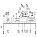
도 2 내지 도 3은 도 1의 Ⅱ-Ⅱ' 및 Ⅲ-Ⅲ'선을 따라 절단한 단면도들이다.
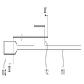
도 4 내지 도 14는 본 발명의 일 실시예에 따른 도 1의 산화물 반도체 박막 트랜지스터를 형성하는 방법을 설명하기위한 배치도 및 단면도들이다.
제1 게이트 절연막 패턴 121a 제2 게이트 절연막 패턴 121b
산화물 반도체 패턴 141 절연막 패턴 171
소스 전극 134 드레인 전극 133
보호 절연막 161 화소 전극 152
Claims (22)
- 게이트 전극,
상기 게이트 전극 위에 위치하는 산화물 반도체 패턴,
상기 게이트 전극과 상기 산화물 반도체 패턴 사이에 위치하며 섬 형이거나 두께가 서로 다른 두 부분을 갖는 제 1 게이트 절연막 패턴
상기 산화물 반도체 패턴 위에 위치하며 서로 이격된 소스 전극 및 드레인 전극 및
상기 소스 전극 및 상기 드레인 전극과 상기 산화물 반도체 패턴 사이에 위치하며, 상기 소스 전극 및 상기 드레인 전극 그리고 상기 제 1 게이트 절연막 패턴과 부분적으로 접하고, 계단 형태의 외곽 부로 둘러싸인 제 1 절연막 패턴을 포함하며,
상기 소스 전극 및 상기 드레인 전극은 상기 산화물 반도체 패턴의 채널 방향 측면과 접하는 박막 트랜지스터. - 제 1 항에 있어서, 상기 계단 형태의 외곽 부는 상기 소스 전극 및 상기 드레인 전극과 접하면서 탄소를 포함하는고분자 화합물로 이루어진 막을 더 포함하는 박막 트랜지스터.
- 제 1항에 있어서, 상기 제 1 게이트 절연막 패턴은 실리콘 산화막인 박막 트랜지스터
- 제 3 항에 있어서, 상기 게이트 전극과 상기 산화물 반도체 패턴은 적어도 1000Å 이상 이격되어 있는 박막 트랜지스터.
- 제 3항에 있어서, 상기 제 1 절연막 패턴은 실리콘 산화막인 박막 트랜지스터
- 제 5항에 있어서, 상기 제 1 절연막 패턴의 두께는 3000Å 이하인 박막 트랜지스터.
- 제 5 항에 있어서, 상기 계단 형태의 외곽 부는 상기 소스 전극 및 상기 드레인 전극과 접하면서, 탄소를 포함하는고분자 화합물로 이루어진 막을 더 포함하는 박막 트랜지스터.
- 제 1항에 있어서, 상기 게이트 전극과 상기 제1 게이트 절연막 패턴 사이에 위치하는 제 2 게이트 절연막을 더 포함하는 박막 트랜지스터.
- 제 8항에 있어서, 상기 제 2 게이트 절연막은 상기 게이트 전극과 접하며, 실리콘 질화막인 박막 트랜지스터.
- 제 9항에 있어서, 상기 제 2 게이트 절연막의 두께는 1000Å 이상인 박막 트랜지스터.
- 게이트 전극을 형성하는 단계,
상기 게이트 전극 상에 제 1 게이트 절연막을 형성하는 단계 ,
상기 제 1 게이트 절연막 상에 산화물 반도체 패턴을 형성하는 단계,
상기 산화물 반도체 패턴 상에 형성되며 상기 제 1 게이트 절연막과 부분적으로 접하는 제 1 절연막 패턴을 형성하는단계
연속하여 상기 제 1 게이트 절연막을 패터닝하여 섬 형이거나 두께가 서로 다른 두 부분을 갖는 제 1 게이트 절연막 패턴을 형성하는 단계
상기 제 1 절연막 패턴을 부분 식각 하여 상기 제1 게이트 절연막과 부분적으로 접하며, 계단 형태의 외곽 부로 둘러싸인 제 2 절연막 패턴을 형성하는 단계 및
상기 산화물 반도체 패턴과 전기적으로 연결되고, 상기 제 2 절연막 패턴과 부분적으로 접하며 서로 떨어져 위치하는 소스 전극 및 드레인 전극을 형성하는 단계를 포함하고,
상기 소스 전극 및 상기 드레인 전극은 상기 산화물 반도체 패턴의 채널 방향 측면과 접하는 박막 트랜지스터 형성방법. - 제 11항에 있어서, 상기 제 1 게이트 절연막 패턴은 실리콘 산화막인 박막 트랜지스터 형성방법.
- 제 12항에 있어서, 상기 제 2 절연막 패턴은 실리콘 산화막인 박막 트랜지스터 형성방법.
- 제 13항에 있어서, 상기 제 2 절연막 패턴의 두께는 3000Å 이하인 박막 트랜지스터 형성방법.
- 제 11항에 있어서, 상기 제 1 절연막 패턴을 형성하는 단계 및 섬 형의 제 1 게이트 절연막 패턴을 형성하는단계는
할로겐 탄소 화합물 및 산소 가스를 원료 가스로 하는 제 1 식각 공정인 박막 트랜지스터 형성방법. - 제 15항에 있어서, 상기 제 1 식각 공정은 할로겐 황 화합물을 원료 가스로 더 포함하며, 할로겐 황 화합물을 할로겐 탄소 화합물 및 산소 가스 유량 대비 20%이하의 유량으로 공급하는박막 트랜지스터 형성방법.
- 제 16항에 있어서, 상기 할로겐 탄소 화합물은 C4F8인 박막트랜지스터 형성방법
- 제 11항에 있어서, 상기 제 1 절연막 패턴을 부분 식각 하여 계단 형태의 외곽 부로 둘러싸인 제 2 절연막 패턴을 형성하는 단계는
제 1 절연막 패턴 표면에 형성된 탄소를 포함하는 고분자 화합물을 제거하는 단계
고분자 화합물이 제거된 상기 제 1 절연막 패턴을 부분 식각하며, 외곽 부에 탄소를 포함하는 고분자 화합물을 형성하는단계를 포함하는 박막 트랜지스터 형성방법. - 제 18항에 있어서, 상기 고분자 화합물을 제거하는 단계는 불활성 가스 및 산소 가스를 원료 가스로 하는 제 2 식각 공정인 박막 트랜지스터 형성방법.
- 제 18항에 있어서, 상기 고분자 화합물이 제거된 상기 제 1 절연막 패턴을 부분 식각하며, 외곽 부에 탄소를 포함하는 고분자 화합물을 형성하는단계는
할로겐 탄소 화합물 및 산소 가스를 원료 가스로 하는 제 3 식각 공정인 박막 트랜지스터 형성방법. - 제 20항에 있어서, 상기 제 3 식각 공정은 할로겐 탄소 화합물을 산소 가스 유량 대비 동등 또는 그 이상으로 공급하는 박막 트랜지스터 형성방법.
- 제 21항에 있어서, 상기 할로겐 탄소 화합물은 C4F8인 박막트랜지스터 형성방법
Priority Applications (4)
| Application Number | Priority Date | Filing Date | Title |
|---|---|---|---|
| KR1020100013611A KR101636998B1 (ko) | 2010-02-12 | 2010-02-12 | 박막 트랜지스터 및 그 제조 방법 |
| US12/902,786 US8853699B2 (en) | 2010-02-12 | 2010-10-12 | Thin film transistor and method of forming the same |
| TW099136178A TWI532186B (zh) | 2010-02-12 | 2010-10-22 | 薄膜電晶體及其形成方法 |
| JP2010280796A JP5690574B2 (ja) | 2010-02-12 | 2010-12-16 | 薄膜トランジスター及びその形成方法 |
Applications Claiming Priority (1)
| Application Number | Priority Date | Filing Date | Title |
|---|---|---|---|
| KR1020100013611A KR101636998B1 (ko) | 2010-02-12 | 2010-02-12 | 박막 트랜지스터 및 그 제조 방법 |
Publications (2)
| Publication Number | Publication Date |
|---|---|
| KR20110093511A KR20110093511A (ko) | 2011-08-18 |
| KR101636998B1 true KR101636998B1 (ko) | 2016-07-08 |
Family
ID=44369015
Family Applications (1)
| Application Number | Title | Priority Date | Filing Date |
|---|---|---|---|
| KR1020100013611A Active KR101636998B1 (ko) | 2010-02-12 | 2010-02-12 | 박막 트랜지스터 및 그 제조 방법 |
Country Status (4)
| Country | Link |
|---|---|
| US (1) | US8853699B2 (ko) |
| JP (1) | JP5690574B2 (ko) |
| KR (1) | KR101636998B1 (ko) |
| TW (1) | TWI532186B (ko) |
Families Citing this family (14)
| Publication number | Priority date | Publication date | Assignee | Title |
|---|---|---|---|---|
| KR102089200B1 (ko) | 2009-11-28 | 2020-03-13 | 가부시키가이샤 한도오따이 에네루기 켄큐쇼 | 반도체 장치 및 그 제조 방법 |
| KR20120045178A (ko) * | 2010-10-29 | 2012-05-09 | 삼성전자주식회사 | 박막 트랜지스터 및 이의 제조 방법 |
| KR20120063809A (ko) * | 2010-12-08 | 2012-06-18 | 삼성전자주식회사 | 박막 트랜지스터 표시판 |
| US9660092B2 (en) * | 2011-08-31 | 2017-05-23 | Semiconductor Energy Laboratory Co., Ltd. | Oxide semiconductor thin film transistor including oxygen release layer |
| KR101951296B1 (ko) * | 2011-12-06 | 2019-04-26 | 엘지디스플레이 주식회사 | 산화물 반도체층을 갖는 박막트랜지스터 및 이를 구비한 어레이 기판 |
| US9040981B2 (en) * | 2012-01-20 | 2015-05-26 | Semiconductor Energy Laboratory Co., Ltd. | Semiconductor device |
| CN102629591B (zh) * | 2012-02-28 | 2015-10-21 | 京东方科技集团股份有限公司 | 一种阵列基板的制造方法及阵列基板、显示器 |
| JP2013229453A (ja) * | 2012-04-26 | 2013-11-07 | Sony Corp | 半導体装置、表示装置及び半導体装置の製造方法 |
| CN107403840B (zh) * | 2012-05-10 | 2021-05-11 | 株式会社半导体能源研究所 | 半导体装置 |
| KR101976133B1 (ko) * | 2012-11-20 | 2019-05-08 | 삼성디스플레이 주식회사 | 표시 장치 |
| JPWO2015025499A1 (ja) * | 2013-08-19 | 2017-03-02 | 出光興産株式会社 | 酸化物半導体基板及びショットキーバリアダイオード |
| KR102293595B1 (ko) * | 2015-03-24 | 2021-08-25 | 삼성디스플레이 주식회사 | 박막 트랜지스터 표시판 및 그 제조 방법 |
| JP6611521B2 (ja) * | 2015-08-25 | 2019-11-27 | 三菱電機株式会社 | 薄膜トランジスタ及びアレイ基板 |
| KR20170131787A (ko) * | 2016-05-20 | 2017-11-30 | 삼성디스플레이 주식회사 | 박막트랜지스터의 제조방법 및 박막트랜지스터를 채용하는 표시장치 |
Citations (2)
| Publication number | Priority date | Publication date | Assignee | Title |
|---|---|---|---|---|
| JP2007123861A (ja) * | 2005-09-29 | 2007-05-17 | Semiconductor Energy Lab Co Ltd | 半導体装置及びその作製方法 |
| US20100032664A1 (en) | 2008-08-06 | 2010-02-11 | Samsung Electronics Co., Ltd. | Thin film transistor substrate and a fabricating method thereof |
Family Cites Families (21)
| Publication number | Priority date | Publication date | Assignee | Title |
|---|---|---|---|---|
| JPS6237935A (ja) | 1985-08-13 | 1987-02-18 | Matsushita Electric Ind Co Ltd | 平坦化ドライエツチング方法 |
| US5354386A (en) | 1989-03-24 | 1994-10-11 | National Semiconductor Corporation | Method for plasma etching tapered and stepped vias |
| JP3208596B2 (ja) | 1992-04-01 | 2001-09-17 | ソニー株式会社 | ドライエッチング方法 |
| JPH0918006A (ja) | 1995-07-03 | 1997-01-17 | Citizen Watch Co Ltd | 薄膜トランジスタおよびその製造方法 |
| JP3801687B2 (ja) | 1996-06-06 | 2006-07-26 | 三菱電機株式会社 | 薄膜トランジスタおよびその製法 |
| JPH10209458A (ja) | 1997-01-22 | 1998-08-07 | Mitsubishi Electric Corp | 液晶表示装置とこれに用いられる薄膜トランジスタ及びその製造方法 |
| JP2000036491A (ja) | 1998-05-15 | 2000-02-02 | Fujitsu Ltd | 半導体装置の製造方法 |
| US6184119B1 (en) | 1999-03-15 | 2001-02-06 | Vlsi Technology, Inc. | Methods for reducing semiconductor contact resistance |
| JP2001119029A (ja) | 1999-10-18 | 2001-04-27 | Fujitsu Ltd | 薄膜トランジスタ及びその製造方法及びそれを備えた液晶表示装置 |
| JP2002134756A (ja) | 2000-10-26 | 2002-05-10 | Matsushita Electric Ind Co Ltd | 半導体装置およびその製造方法 |
| KR100404479B1 (ko) | 2001-06-21 | 2003-11-05 | 주식회사 하이닉스반도체 | 듀얼 다마신 배선 형성방법 |
| US7265056B2 (en) * | 2004-01-09 | 2007-09-04 | Taiwan Semiconductor Manufacturing Company, Ltd. | Method for forming novel BARC open for precision critical dimension control |
| EP1998373A3 (en) * | 2005-09-29 | 2012-10-31 | Semiconductor Energy Laboratory Co, Ltd. | Semiconductor device having oxide semiconductor layer and manufacturing method thereof |
| TWI275183B (en) * | 2006-01-12 | 2007-03-01 | Ind Tech Res Inst | Structure of thin film transistor array and method for making the same |
| KR101226974B1 (ko) | 2006-05-03 | 2013-01-28 | 엘지디스플레이 주식회사 | 액정표시장치용 어레이 기판 및 그 제조 방법 |
| US7938931B2 (en) | 2006-05-24 | 2011-05-10 | Lam Research Corporation | Edge electrodes with variable power |
| KR101146574B1 (ko) * | 2006-12-05 | 2012-05-16 | 캐논 가부시끼가이샤 | 산화물 반도체를 이용한 박막 트랜지스터의 제조방법 및 표시장치 |
| JP4626659B2 (ja) * | 2008-03-13 | 2011-02-09 | ソニー株式会社 | 表示装置 |
| JP5704790B2 (ja) | 2008-05-07 | 2015-04-22 | キヤノン株式会社 | 薄膜トランジスタ、および、表示装置 |
| KR100963027B1 (ko) * | 2008-06-30 | 2010-06-10 | 삼성모바일디스플레이주식회사 | 박막 트랜지스터, 그의 제조 방법 및 박막 트랜지스터를구비하는 평판 표시 장치 |
| JP5123141B2 (ja) * | 2008-11-19 | 2013-01-16 | 株式会社東芝 | 表示装置 |
-
2010
- 2010-02-12 KR KR1020100013611A patent/KR101636998B1/ko active Active
- 2010-10-12 US US12/902,786 patent/US8853699B2/en active Active
- 2010-10-22 TW TW099136178A patent/TWI532186B/zh active
- 2010-12-16 JP JP2010280796A patent/JP5690574B2/ja active Active
Patent Citations (2)
| Publication number | Priority date | Publication date | Assignee | Title |
|---|---|---|---|---|
| JP2007123861A (ja) * | 2005-09-29 | 2007-05-17 | Semiconductor Energy Lab Co Ltd | 半導体装置及びその作製方法 |
| US20100032664A1 (en) | 2008-08-06 | 2010-02-11 | Samsung Electronics Co., Ltd. | Thin film transistor substrate and a fabricating method thereof |
Also Published As
| Publication number | Publication date |
|---|---|
| TWI532186B (zh) | 2016-05-01 |
| JP5690574B2 (ja) | 2015-03-25 |
| KR20110093511A (ko) | 2011-08-18 |
| JP2011166120A (ja) | 2011-08-25 |
| US20110198603A1 (en) | 2011-08-18 |
| US8853699B2 (en) | 2014-10-07 |
| TW201128779A (en) | 2011-08-16 |
Similar Documents
| Publication | Publication Date | Title |
|---|---|---|
| KR101636998B1 (ko) | 박막 트랜지스터 및 그 제조 방법 | |
| KR101533391B1 (ko) | 박막 트랜지스터 기판과 그 제조 방법 | |
| US20110183463A1 (en) | Thin film transitor substrate and method of manufacturing the same | |
| US9726940B2 (en) | Active matrix substrate manufacturing method, display apparatus manufacturing method, and display apparatus | |
| KR101790176B1 (ko) | 어레이 기판의 제조방법 | |
| US20090225249A1 (en) | Thin film transistor array substrate and manufacturing method thereof | |
| CN100517729C (zh) | 薄膜晶体管衬底及其制造方法 | |
| US8193534B2 (en) | Array substrate of thin film transistor liquid crystal display and method of manufacturing the same | |
| JP2011258949A (ja) | 薄膜トランジスタ表示板及びその製造方法 | |
| US20140120657A1 (en) | Back Channel Etching Oxide Thin Film Transistor Process Architecture | |
| KR20100063493A (ko) | 박막 트랜지스터 기판 및 그 제조 방법 | |
| US9842915B2 (en) | Array substrate for liquid crystal display device and method of manufacturing the same | |
| US20090174834A1 (en) | Liquid crystal display and method of fabricating the same | |
| US6853405B2 (en) | Method of fabricating liquid crystal display | |
| US7638375B2 (en) | Method of manufacturing thin film transistor substrate | |
| JP2011186424A (ja) | 液晶表示装置のアレイ基板及びその製造方法 | |
| KR20150010065A (ko) | 산화물 반도체 소자의 제조 방법 및 산화물 반도체 소자를 포함하는 표시 장치의 제조 방법 | |
| CN100580906C (zh) | 制造薄膜晶体管基板的方法 | |
| KR20100070082A (ko) | 박막 트랜지스터 표시판 및 이의 제조 방법 | |
| US7125756B2 (en) | Method for fabricating liquid crystal display device | |
| KR20120067108A (ko) | 어레이 기판 및 이의 제조방법 | |
| US9035303B2 (en) | Semiconductor device and method for manufacturing same | |
| US20150048360A1 (en) | Semiconductor device and semiconductor device manufacturing method | |
| KR102120171B1 (ko) | 산화물 박막트랜지스터 어레이 기판 및 그 제조방법 | |
| CN1901209B (zh) | 薄膜晶体管阵列面板及其制造方法 |
Legal Events
| Date | Code | Title | Description |
|---|---|---|---|
| PA0109 | Patent application |
Patent event code: PA01091R01D Comment text: Patent Application Patent event date: 20100212 |
|
| PG1501 | Laying open of application | ||
| N231 | Notification of change of applicant | ||
| PN2301 | Change of applicant |
Patent event date: 20120913 Comment text: Notification of Change of Applicant Patent event code: PN23011R01D |
|
| A201 | Request for examination | ||
| PA0201 | Request for examination |
Patent event code: PA02012R01D Patent event date: 20141218 Comment text: Request for Examination of Application Patent event code: PA02011R01I Patent event date: 20100212 Comment text: Patent Application |
|
| E902 | Notification of reason for refusal | ||
| PE0902 | Notice of grounds for rejection |
Comment text: Notification of reason for refusal Patent event date: 20151209 Patent event code: PE09021S01D |
|
| E701 | Decision to grant or registration of patent right | ||
| PE0701 | Decision of registration |
Patent event code: PE07011S01D Comment text: Decision to Grant Registration Patent event date: 20160331 |
|
| GRNT | Written decision to grant | ||
| PR0701 | Registration of establishment |
Comment text: Registration of Establishment Patent event date: 20160630 Patent event code: PR07011E01D |
|
| PR1002 | Payment of registration fee |
Payment date: 20160630 End annual number: 3 Start annual number: 1 |
|
| PG1601 | Publication of registration | ||
| FPAY | Annual fee payment |
Payment date: 20190529 Year of fee payment: 4 |
|
| PR1001 | Payment of annual fee |
Payment date: 20190529 Start annual number: 4 End annual number: 4 |
|
| FPAY | Annual fee payment |
Payment date: 20200527 Year of fee payment: 5 |
|
| PR1001 | Payment of annual fee |
Payment date: 20200527 Start annual number: 5 End annual number: 5 |
|
| FPAY | Annual fee payment |
Payment date: 20210601 Year of fee payment: 6 |
|
| PR1001 | Payment of annual fee |
Payment date: 20210601 Start annual number: 6 End annual number: 6 |
|
| FPAY | Annual fee payment |
Payment date: 20220523 Year of fee payment: 7 |
|
| PR1001 | Payment of annual fee |
Payment date: 20220523 Start annual number: 7 End annual number: 7 |
|
| PR1001 | Payment of annual fee |
Payment date: 20230524 Start annual number: 8 End annual number: 8 |