CN100399390C - image display device - Google Patents
image display device Download PDFInfo
- Publication number
- CN100399390C CN100399390C CNB021559864A CN02155986A CN100399390C CN 100399390 C CN100399390 C CN 100399390C CN B021559864 A CNB021559864 A CN B021559864A CN 02155986 A CN02155986 A CN 02155986A CN 100399390 C CN100399390 C CN 100399390C
- Authority
- CN
- China
- Prior art keywords
- mentioned
- signal data
- shows signal
- pixel
- image display
- Prior art date
- Legal status (The legal status is an assumption and is not a legal conclusion. Google has not performed a legal analysis and makes no representation as to the accuracy of the status listed.)
- Expired - Lifetime
Links
Images


Classifications
-
- G—PHYSICS
- G09—EDUCATION; CRYPTOGRAPHY; DISPLAY; ADVERTISING; SEALS
- G09G—ARRANGEMENTS OR CIRCUITS FOR CONTROL OF INDICATING DEVICES USING STATIC MEANS TO PRESENT VARIABLE INFORMATION
- G09G3/00—Control arrangements or circuits, of interest only in connection with visual indicators other than cathode-ray tubes
- G09G3/20—Control arrangements or circuits, of interest only in connection with visual indicators other than cathode-ray tubes for presentation of an assembly of a number of characters, e.g. a page, by composing the assembly by combination of individual elements arranged in a matrix no fixed position being assigned to or needed to be assigned to the individual characters or partial characters
- G09G3/2007—Display of intermediate tones
- G09G3/2011—Display of intermediate tones by amplitude modulation
-
- G—PHYSICS
- G09—EDUCATION; CRYPTOGRAPHY; DISPLAY; ADVERTISING; SEALS
- G09G—ARRANGEMENTS OR CIRCUITS FOR CONTROL OF INDICATING DEVICES USING STATIC MEANS TO PRESENT VARIABLE INFORMATION
- G09G3/00—Control arrangements or circuits, of interest only in connection with visual indicators other than cathode-ray tubes
- G09G3/20—Control arrangements or circuits, of interest only in connection with visual indicators other than cathode-ray tubes for presentation of an assembly of a number of characters, e.g. a page, by composing the assembly by combination of individual elements arranged in a matrix no fixed position being assigned to or needed to be assigned to the individual characters or partial characters
- G09G3/22—Control arrangements or circuits, of interest only in connection with visual indicators other than cathode-ray tubes for presentation of an assembly of a number of characters, e.g. a page, by composing the assembly by combination of individual elements arranged in a matrix no fixed position being assigned to or needed to be assigned to the individual characters or partial characters using controlled light sources
- G09G3/30—Control arrangements or circuits, of interest only in connection with visual indicators other than cathode-ray tubes for presentation of an assembly of a number of characters, e.g. a page, by composing the assembly by combination of individual elements arranged in a matrix no fixed position being assigned to or needed to be assigned to the individual characters or partial characters using controlled light sources using electroluminescent panels
- G09G3/32—Control arrangements or circuits, of interest only in connection with visual indicators other than cathode-ray tubes for presentation of an assembly of a number of characters, e.g. a page, by composing the assembly by combination of individual elements arranged in a matrix no fixed position being assigned to or needed to be assigned to the individual characters or partial characters using controlled light sources using electroluminescent panels semiconductive, e.g. using light-emitting diodes [LED]
- G09G3/3208—Control arrangements or circuits, of interest only in connection with visual indicators other than cathode-ray tubes for presentation of an assembly of a number of characters, e.g. a page, by composing the assembly by combination of individual elements arranged in a matrix no fixed position being assigned to or needed to be assigned to the individual characters or partial characters using controlled light sources using electroluminescent panels semiconductive, e.g. using light-emitting diodes [LED] organic, e.g. using organic light-emitting diodes [OLED]
- G09G3/3225—Control arrangements or circuits, of interest only in connection with visual indicators other than cathode-ray tubes for presentation of an assembly of a number of characters, e.g. a page, by composing the assembly by combination of individual elements arranged in a matrix no fixed position being assigned to or needed to be assigned to the individual characters or partial characters using controlled light sources using electroluminescent panels semiconductive, e.g. using light-emitting diodes [LED] organic, e.g. using organic light-emitting diodes [OLED] using an active matrix
- G09G3/3233—Control arrangements or circuits, of interest only in connection with visual indicators other than cathode-ray tubes for presentation of an assembly of a number of characters, e.g. a page, by composing the assembly by combination of individual elements arranged in a matrix no fixed position being assigned to or needed to be assigned to the individual characters or partial characters using controlled light sources using electroluminescent panels semiconductive, e.g. using light-emitting diodes [LED] organic, e.g. using organic light-emitting diodes [OLED] using an active matrix with pixel circuitry controlling the current through the light-emitting element
-
- G—PHYSICS
- G09—EDUCATION; CRYPTOGRAPHY; DISPLAY; ADVERTISING; SEALS
- G09G—ARRANGEMENTS OR CIRCUITS FOR CONTROL OF INDICATING DEVICES USING STATIC MEANS TO PRESENT VARIABLE INFORMATION
- G09G3/00—Control arrangements or circuits, of interest only in connection with visual indicators other than cathode-ray tubes
- G09G3/20—Control arrangements or circuits, of interest only in connection with visual indicators other than cathode-ray tubes for presentation of an assembly of a number of characters, e.g. a page, by composing the assembly by combination of individual elements arranged in a matrix no fixed position being assigned to or needed to be assigned to the individual characters or partial characters
- G09G3/34—Control arrangements or circuits, of interest only in connection with visual indicators other than cathode-ray tubes for presentation of an assembly of a number of characters, e.g. a page, by composing the assembly by combination of individual elements arranged in a matrix no fixed position being assigned to or needed to be assigned to the individual characters or partial characters by control of light from an independent source
- G09G3/36—Control arrangements or circuits, of interest only in connection with visual indicators other than cathode-ray tubes for presentation of an assembly of a number of characters, e.g. a page, by composing the assembly by combination of individual elements arranged in a matrix no fixed position being assigned to or needed to be assigned to the individual characters or partial characters by control of light from an independent source using liquid crystals
- G09G3/3611—Control of matrices with row and column drivers
- G09G3/3648—Control of matrices with row and column drivers using an active matrix
-
- G—PHYSICS
- G09—EDUCATION; CRYPTOGRAPHY; DISPLAY; ADVERTISING; SEALS
- G09G—ARRANGEMENTS OR CIRCUITS FOR CONTROL OF INDICATING DEVICES USING STATIC MEANS TO PRESENT VARIABLE INFORMATION
- G09G2300/00—Aspects of the constitution of display devices
- G09G2300/04—Structural and physical details of display devices
- G09G2300/0404—Matrix technologies
- G09G2300/0417—Special arrangements specific to the use of low carrier mobility technology
-
- G—PHYSICS
- G09—EDUCATION; CRYPTOGRAPHY; DISPLAY; ADVERTISING; SEALS
- G09G—ARRANGEMENTS OR CIRCUITS FOR CONTROL OF INDICATING DEVICES USING STATIC MEANS TO PRESENT VARIABLE INFORMATION
- G09G2300/00—Aspects of the constitution of display devices
- G09G2300/08—Active matrix structure, i.e. with use of active elements, inclusive of non-linear two terminal elements, in the pixels together with light emitting or modulating elements
- G09G2300/0809—Several active elements per pixel in active matrix panels
- G09G2300/0819—Several active elements per pixel in active matrix panels used for counteracting undesired variations, e.g. feedback or autozeroing
-
- G—PHYSICS
- G09—EDUCATION; CRYPTOGRAPHY; DISPLAY; ADVERTISING; SEALS
- G09G—ARRANGEMENTS OR CIRCUITS FOR CONTROL OF INDICATING DEVICES USING STATIC MEANS TO PRESENT VARIABLE INFORMATION
- G09G2300/00—Aspects of the constitution of display devices
- G09G2300/08—Active matrix structure, i.e. with use of active elements, inclusive of non-linear two terminal elements, in the pixels together with light emitting or modulating elements
- G09G2300/0809—Several active elements per pixel in active matrix panels
- G09G2300/0842—Several active elements per pixel in active matrix panels forming a memory circuit, e.g. a dynamic memory with one capacitor
- G09G2300/0861—Several active elements per pixel in active matrix panels forming a memory circuit, e.g. a dynamic memory with one capacitor with additional control of the display period without amending the charge stored in a pixel memory, e.g. by means of additional select electrodes
-
- G—PHYSICS
- G09—EDUCATION; CRYPTOGRAPHY; DISPLAY; ADVERTISING; SEALS
- G09G—ARRANGEMENTS OR CIRCUITS FOR CONTROL OF INDICATING DEVICES USING STATIC MEANS TO PRESENT VARIABLE INFORMATION
- G09G2310/00—Command of the display device
- G09G2310/02—Addressing, scanning or driving the display screen or processing steps related thereto
- G09G2310/0243—Details of the generation of driving signals
- G09G2310/0259—Details of the generation of driving signals with use of an analog or digital ramp generator in the column driver or in the pixel circuit
-
- G—PHYSICS
- G09—EDUCATION; CRYPTOGRAPHY; DISPLAY; ADVERTISING; SEALS
- G09G—ARRANGEMENTS OR CIRCUITS FOR CONTROL OF INDICATING DEVICES USING STATIC MEANS TO PRESENT VARIABLE INFORMATION
- G09G2310/00—Command of the display device
- G09G2310/02—Addressing, scanning or driving the display screen or processing steps related thereto
- G09G2310/0264—Details of driving circuits
- G09G2310/027—Details of drivers for data electrodes, the drivers handling digital grey scale data, e.g. use of D/A converters
-
- G—PHYSICS
- G09—EDUCATION; CRYPTOGRAPHY; DISPLAY; ADVERTISING; SEALS
- G09G—ARRANGEMENTS OR CIRCUITS FOR CONTROL OF INDICATING DEVICES USING STATIC MEANS TO PRESENT VARIABLE INFORMATION
- G09G2310/00—Command of the display device
- G09G2310/06—Details of flat display driving waveforms
-
- G—PHYSICS
- G09—EDUCATION; CRYPTOGRAPHY; DISPLAY; ADVERTISING; SEALS
- G09G—ARRANGEMENTS OR CIRCUITS FOR CONTROL OF INDICATING DEVICES USING STATIC MEANS TO PRESENT VARIABLE INFORMATION
- G09G2320/00—Control of display operating conditions
- G09G2320/02—Improving the quality of display appearance
- G09G2320/0252—Improving the response speed
-
- G—PHYSICS
- G09—EDUCATION; CRYPTOGRAPHY; DISPLAY; ADVERTISING; SEALS
- G09G—ARRANGEMENTS OR CIRCUITS FOR CONTROL OF INDICATING DEVICES USING STATIC MEANS TO PRESENT VARIABLE INFORMATION
- G09G2320/00—Control of display operating conditions
- G09G2320/04—Maintaining the quality of display appearance
- G09G2320/043—Preventing or counteracting the effects of ageing
-
- G—PHYSICS
- G09—EDUCATION; CRYPTOGRAPHY; DISPLAY; ADVERTISING; SEALS
- G09G—ARRANGEMENTS OR CIRCUITS FOR CONTROL OF INDICATING DEVICES USING STATIC MEANS TO PRESENT VARIABLE INFORMATION
- G09G3/00—Control arrangements or circuits, of interest only in connection with visual indicators other than cathode-ray tubes
- G09G3/20—Control arrangements or circuits, of interest only in connection with visual indicators other than cathode-ray tubes for presentation of an assembly of a number of characters, e.g. a page, by composing the assembly by combination of individual elements arranged in a matrix no fixed position being assigned to or needed to be assigned to the individual characters or partial characters
- G09G3/2007—Display of intermediate tones
- G09G3/2014—Display of intermediate tones by modulation of the duration of a single pulse during which the logic level remains constant
-
- G—PHYSICS
- G09—EDUCATION; CRYPTOGRAPHY; DISPLAY; ADVERTISING; SEALS
- G09G—ARRANGEMENTS OR CIRCUITS FOR CONTROL OF INDICATING DEVICES USING STATIC MEANS TO PRESENT VARIABLE INFORMATION
- G09G3/00—Control arrangements or circuits, of interest only in connection with visual indicators other than cathode-ray tubes
- G09G3/20—Control arrangements or circuits, of interest only in connection with visual indicators other than cathode-ray tubes for presentation of an assembly of a number of characters, e.g. a page, by composing the assembly by combination of individual elements arranged in a matrix no fixed position being assigned to or needed to be assigned to the individual characters or partial characters
- G09G3/2007—Display of intermediate tones
- G09G3/2018—Display of intermediate tones by time modulation using two or more time intervals
- G09G3/2022—Display of intermediate tones by time modulation using two or more time intervals using sub-frames
-
- G—PHYSICS
- G09—EDUCATION; CRYPTOGRAPHY; DISPLAY; ADVERTISING; SEALS
- G09G—ARRANGEMENTS OR CIRCUITS FOR CONTROL OF INDICATING DEVICES USING STATIC MEANS TO PRESENT VARIABLE INFORMATION
- G09G3/00—Control arrangements or circuits, of interest only in connection with visual indicators other than cathode-ray tubes
- G09G3/20—Control arrangements or circuits, of interest only in connection with visual indicators other than cathode-ray tubes for presentation of an assembly of a number of characters, e.g. a page, by composing the assembly by combination of individual elements arranged in a matrix no fixed position being assigned to or needed to be assigned to the individual characters or partial characters
- G09G3/2007—Display of intermediate tones
- G09G3/2077—Display of intermediate tones by a combination of two or more gradation control methods
Landscapes
- Engineering & Computer Science (AREA)
- Physics & Mathematics (AREA)
- Computer Hardware Design (AREA)
- General Physics & Mathematics (AREA)
- Theoretical Computer Science (AREA)
- Chemical & Material Sciences (AREA)
- Crystallography & Structural Chemistry (AREA)
- Control Of El Displays (AREA)
- Control Of Indicators Other Than Cathode Ray Tubes (AREA)
- Electroluminescent Light Sources (AREA)
- Liquid Crystal (AREA)
- Liquid Crystal Display Device Control (AREA)
Abstract
提供一种图象显示装置,可避免微小噪声或驱动频率高速化的问题,同时可进行多灰度等级的高精度显示。构成1帧的显示信号数据,由多个子帧,例如4个子帧1/4到4/4构成,1/4帧定为模拟信号的寻址期间,2/4帧定为模拟灰度等级显示期间,3/4帧定为数字信号的寻址期间,4/4帧定为数字灰度等级发光期间。把图象显示装置构成为使得模拟灰度等级显示期间,象素(6)内的OLED元件(4),借助于模拟驱动信号电路(12)进行与写入象素内的存储电容(1)中的模拟信号电压对应的时间的发光,数字灰度等级显示期间,借助于数字信号驱动电路(16),与写入存储电容(1)中的数字信号电压相对应地进行发光/非发光的两值的发光动作。
To provide an image display device capable of performing multi-gray-scale high-precision display while avoiding the problems of minute noise and high-speed driving frequency. The display signal data constituting one frame is composed of multiple subframes, such as four subframes 1/4 to 4/4, 1/4 frame is defined as the addressing period of the analog signal, and 2/4 frame is defined as the analog grayscale display During the period, 3/4 frame is defined as the addressing period of the digital signal, and 4/4 frame is defined as the digital grayscale light emitting period. The image display device is configured such that during the analog grayscale display period, the OLED element (4) in the pixel (6) is written into the storage capacitor (1) in the pixel by means of an analog drive signal circuit (12). During the digital grayscale display period, by means of the digital signal drive circuit (16), the digital signal voltage written in the storage capacitor (1) is correspondingly luminous/non-luminous. Two-valued glow action.
Description
技术领域 technical field
本发明涉及可进行多灰度等级显示的图象显示装置,特别是涉及适合于高灰度等级显示的图象显示装置。The present invention relates to an image display device capable of displaying multiple gray levels, in particular to an image display device suitable for high gray level display.
背景技术 Background technique
以下,用图16-图18对两个现有技术进行说明。Hereinafter, two prior art techniques will be described with reference to FIGS. 16 to 18 .
图16是使用第1现有技术的发光显示元件(以下,叫作第1现有例)的构成图。具有作为象素发光体的有机EL(电致发光)元件204的象素205在显示部分上被配置成矩阵状。象素205通过栅极线206、源极线207、电源线208等被连接到外部的驱动电路上。在各个象素205中,源极线207通过逻辑TFT(薄膜晶0体管)201连接到电力TFT203的栅极和存储电容202的一端上,电力TFT203的一端和存储电容202的另一端共同连接到电源线208上。Fig. 16 is a configuration diagram of a light-emitting display device using the first conventional technology (hereinafter referred to as the first conventional example).
此外,电力TFT203的另一端通过有机EL元件204连接到共用电源端子上。栅极线206的一端连接到帧扫描电路210上,源极线207的一端连接到模拟信号电压输入电路209上。另外在这里逻辑TFT201和电力TFT203,用Si-TFT在SiO2基板上形成。In addition, the other end of the power TFT 203 is connected to a common power supply terminal through the
下面,说明这样地构成的第1现有例的动作。Next, the operation of the first conventional example thus configured will be described.
采用帧扫描电路210通过栅极线206使规定的象素行的逻辑TFT201进行开闭的办法,从模拟信号电压输入电路209输入到源极线207上的模拟信号电压,被输入给电力TFT203的栅极和存储电容202上,在一直到进行其次的扫描写入为止的1帧期间内进行保持。电力TFT203,把与上述模拟信号电压对应的模拟信号电流输入至有机EL元件204。借助于此,有机EL元件204就以与上述模拟信号电压对应的辉度发光。Adopt
关于上述第1现有例的技术,例如,在特开平8-241048号公报中详细地进行了讲述。另外,在现有例的说明中,上述发光元件虽然与该公报相一致地使用了有机EL元件这样的术语,但是,由于近些年来大多被称之为有机发光二极管,故在本说明书中,以下也使用后者的术语。The technique of the above-mentioned first conventional example is described in detail in, for example, JP-A-8-241048. In addition, in the description of the conventional example, although the term "organic EL element" was used for the above-mentioned light-emitting element in conformity with this publication, since it is often referred to as an organic light-emitting diode in recent years, in this specification, The latter term is also used below.
其次,用图17和图18说明另外的现有技术。Next, another prior art will be described with reference to FIGS. 17 and 18 .
图17是使用第2现有技术的发光显示器件(以下,叫做第2现有例)的构成图。该第2现有例的构造,基本上与上述第1现有例中说明的构造是同样的,不同的是设置数字信号电压输入电路211来代替模拟信号电压输入电路209,设置子帧扫描电路212来代替帧扫描电路212。因此,在这里仅仅对因这些不同产生的动作上的差异进行说明。Fig. 17 is a configuration diagram of a light-emitting display device using a second conventional technology (hereinafter referred to as a second conventional example). The structure of this second conventional example is basically the same as that described in the above-mentioned first conventional example, except that a digital signal voltage input circuit 211 is provided instead of the analog signal
用图18说明第2现有例的动作。如图18所示,在本现有例中,显示1张画面信息的1帧期间,被分割成多个子帧期间。此外,该子帧期间,由作为向各个象素写入显示信号的期间的寻址期间Ts,和根据所写入的显示信号进行发光/非发光显示的确认期间T1~Tn(为使说明简单起见,在图18中用n=5表示)构成。在寻址期间Ts内OLED元件的驱动电压为OFF电平,根本不发光。在这里,在各个寻址期间内的向各个象素写入的显示信号动作,基本上与上述第1现有例是同样的,但象素信号不是模拟信号,是‘高电平’或‘低电平’的二进制的数字信号。The operation of the second conventional example will be described with reference to FIG. 18 . As shown in FIG. 18 , in this conventional example, one frame period for displaying one screen information is divided into a plurality of subframe periods. In addition, this subframe period consists of an address period Ts, which is a period in which a display signal is written to each pixel, and a confirmation period T1 to Tn in which light-emitting/non-luminous display is performed according to the written display signal (for simplicity of description). For the sake of consideration, it is represented by n=5 in FIG. 18 ). During the address period Ts, the driving voltage of the OLED element is OFF level, and does not emit light at all. Here, the display signal operation written to each pixel in each address period is basically the same as that of the above-mentioned first conventional example, but the pixel signal is not an analog signal, but a 'high level' or ' Low level' binary digital signal.
因此,在跟在寻址期间Ts后边的确认期间T1~T5中的OLED元件的发光,也是‘ON’或‘OFF ‘的数字发光。在这里,如图18所示,在各个子帧的确认期间T1~T5中,由于已赋予2的i次方的时间加权,故可以给各个发光位加权。借助于此,在第2现有例中,就可以进行与数字数据的各位对应的中间色调显示。Therefore, the light emission of the OLED elements in the verification period T1-T5 following the address period Ts is also digital light emission of 'ON' or 'OFF'. Here, as shown in FIG. 18 , in the confirmation periods T1 to T5 of each subframe, since a time weight of 2 to the power of i is given, weighting can be given to each light-emitting bit. With this, in the second conventional example, halftone display corresponding to each bit of digital data can be performed.
该现有例的优点在于,由于仅仅把电力TFT203用做开关,故阈值电压等的电力TFT的特性波动,不能在发光时的辉度中反映出来。借助于此,在本现有例中,可以进行辉度波动小、高画质的显示。另外,关于这样的现有技术,例如,已在特开2001-159878号公报中详细地进行了讲述。The advantage of this conventional example is that since only the
发明内容 Contents of the invention
对于上述现有技术的延伸,要想提供实现今后TV等的用途上必须的6位或8位等的多灰度等级显示的图象显示装置,是有困难的。以下对此进行说明。It is difficult to provide an image display device that realizes multi-gradation display such as 6-bit or 8-bit, which is necessary for future TV and other applications, by extension of the above-mentioned prior art. This is explained below.
在图16所示的第1现有例中,用电力TFT203驱动作为电流驱动型的元件的有机EL元件204。该电力TFT203虽然起着电压输入的电流输出元件的作用,但是如果在电力TFT203的阈值电压Vth中存在着波动,由于该波动成分将加到输入的信号电压上去,故在每一象素中都将产生辉度的不均匀。In the first conventional example shown in FIG. 16 , an
一般地说,TFT与单晶硅元件比较起来,每个元件间的波动大,特别是在象象素那样精心制作多个TFT的情况下,要抑制各个元件间的特性波动是非常困难的。例如,在低温多晶Si-TFT的情况下,已公知将产生以1V为单位的Vth的波动。另一方面,一般地说,OLED元件的发光特性对于输入电压是敏感的,1V的输入电压的不同,常常会带来发光辉度近一倍的变化,故在中间色调显示的情况下,这样的辉度不均匀是不允许的。为此,在第1现有例中,需要正确的辉度控制的多灰度等级中间色调显示是困难的。Generally speaking, TFTs have larger fluctuations among individual elements than single-crystal silicon elements, and it is very difficult to suppress characteristic fluctuations among individual elements especially when a plurality of TFTs are elaborately produced like pixels. For example, in the case of a low-temperature polycrystalline Si-TFT, it is known that Vth fluctuations in units of 1V will occur. On the other hand, generally speaking, the luminous characteristics of OLED elements are sensitive to the input voltage, and the difference in input voltage of 1V often brings about a double change in luminous luminance, so in the case of mid-tone display, such The uneven brightness is not allowed. Therefore, in the first conventional example, multi-gradation halftone display requiring accurate luminance control is difficult.
相对于此,用图17和图18说明的第2现有例,通过对各个象素的OLED元件进行数字控制得到正确的辉度控制。但是如要为了进行多灰度等级中间色调显示而用多位进行这样的数字控制,则需要增加子帧数。例如,在8位显示的情况下,除去8次的确认期间T1~T8之外,还需要与8个子帧对应的8次的寻址期间Ts。为此,就要给子帧扫描电路212加上很大的负担,结果是使得功耗和价格上升。In contrast, in the second conventional example described with reference to FIGS. 17 and 18, accurate luminance control is obtained by digitally controlling the OLED elements of each pixel. However, if such digital control is to be performed with multiple bits for multi-grayscale halftone display, the number of sub-frames needs to be increased. For example, in the case of 8-bit display, eight address periods Ts corresponding to eight subframes are required in addition to eight check periods T1 to T8. For this reason, a large load is imposed on the
此外,若用某种程度大小的大显示面板,由于栅极线206的时间常数界限就会表现出来,故在子帧扫描频率方面存在着物理上的上限。In addition, if a large display panel of a certain size is used, the time constant limit of the
如上所述,即便是使用第2现有例的技术,用于实现多灰度等级中间显示的多位化,存在着驱动上的困难。As described above, even if the technique of the second conventional example is used, there are difficulties in driving for realizing multi-bit multi-gradation intermediate display.
总之,第1现有例那样的‘模拟信号’,由于怕微小的噪声,故难于高精度化,而第2现有例那样的‘数字信号’,由于必须把数据分成子字段,故需要驱动电路的高速化,因而难于高精度化。In short, the "analog signal" like the first conventional example is difficult to achieve high precision because of the fear of minute noise, and the "digital signal" like the second conventional example needs to be driven because the data must be divided into sub-fields. The high speed of the circuit makes it difficult to achieve high precision.
于是,本发明的目的在于提供可以进行用来多灰度等级显示的多位化的图象显示装置。Therefore, an object of the present invention is to provide an image display device capable of multi-bit display for multi-gray scale display.
更具体地,目的在于提供通过同时使用‘模拟信号’和‘数字信号’这两者,在可以避免微小的噪声的问题和驱动频率高速化的问题的同时,实现多灰度等级的高精度显示的图象显示装置。More specifically, the object is to provide a multi-gray scale high-precision display while avoiding the problem of minute noise and the problem of high-speed driving frequency by using both "analog signal" and "digital signal" simultaneously. image display device.
如上所述,听起来有仅仅把现存的‘模拟’和‘数字’组合起来的意思,但是是一种基于与把‘模拟’和‘数字’简单组合的迄今为止的情况完全不同的思考方法的发明,以下,简单地进行说明。As mentioned above, it sounds like just combining the existing 'analog' and 'digital', but it is based on a completely different way of thinking from the conventional situation of simply combining 'analog' and 'digital' The invention is briefly described below.
现有的电子电路中的‘数字’和‘模拟’的同时使用的思考方法,说到底只不过是在同一硅(Si)芯片或组件内同时形成‘数字电路’和‘模拟电路’的混合装配而已。The existing way of thinking about the simultaneous use of 'digital' and 'analog' in electronic circuits is nothing more than a mixed assembly of 'digital circuits' and 'analog circuits' simultaneously formed in the same silicon (Si) chip or package That's all.
与此不同,作成为向‘数字电路’输入‘模拟信号’,或用‘数字电路’驱动‘模拟电路’,比把单一的‘数字电路’或‘模拟电路’混合装配起来的情况下更为高性能化这一设想,在本发明人了解的范围内,迄今为止的图象显示装置中是不曾有过的。本发明,是通过考虑到人的视觉特性不论是模拟显示还是数字显示都感知同样的中间色调这样的显示器的特殊环境条件,采用在同一电路中使‘数字电路’和‘模拟电路’共存的办法,来实现用单一的‘数字电路’或‘模拟电路’难以实现的、高精度、高灰度等级特性这样的从现有常识中设想不到的发明。In contrast, inputting an 'analog signal' to a 'digital circuit' or using a 'digital circuit' to drive an 'analog circuit' is more efficient than combining a single 'digital circuit' or 'analog circuit' The idea of increasing the performance has never occurred in the conventional image display device within the range known by the present inventors. The present invention considers the special environmental conditions of a display such that human visual characteristics perceive the same half tone regardless of the analog display or digital display, and adopts a method of co-existing 'digital circuit' and 'analog circuit' in the same circuit , to realize inventions that cannot be conceived from the existing common sense, such as high precision and high gray scale characteristics, which are difficult to realize with a single 'digital circuit' or 'analog circuit'.
本发明的代表性装置的一个例子如下。就是说,本发明是具有由多个象素构成的显示部分、用来向上述象素写入显示信号数据的信号线、用来从多个上述象素中选择写入输入到上述信号线输入的显示信号数据的象素的写入象素选择装置、用来产生上述显示信号数据的信号数据产生装置的图象显示装置,其特征在于:上述信号数据产生装置,包括用来产生具有三值以上的多值电平的多值显示信号数据的多值信号数据产生装置,构成1帧的上述显示信号数据,由要向由在同一帧期间内显示的多个上述象素构成的象素群输入的多个子帧的显示信号数据构成,在1帧内的至少1个子帧中的上述显示信号数据,具有至少三值的多值电平,就是说,具有三值以上的多值电平。An example of a representative device of the present invention is as follows. That is, the present invention has a display section composed of a plurality of pixels, a signal line for writing display signal data to the pixel, and a signal line for selectively writing input to the signal line from a plurality of the above-mentioned pixels. A pixel selection device for writing display signal data, a signal data generating device for generating the above-mentioned display signal data, and an image display device are characterized in that: the above-mentioned signal data generating device includes a device for generating The multi-valued signal data generating device for the multi-valued display signal data of the above multi-valued level constitutes the above-mentioned display signal data of one frame, and is composed of a pixel group composed of a plurality of the above-mentioned pixels to be displayed in the same frame period The input display signal data of a plurality of subframes is constituted, and the display signal data in at least one subframe within one frame has a multilevel of at least three values, that is, a multilevel of three or more values.
在这里,上述写入象素选择装置,理想的是由多晶Si-TFT构成。Here, the above-mentioned write-in pixel selection means is desirably composed of polycrystalline Si-TFT.
此外,上述子帧中的上述显示信号数据,也可以作成为全都具有三值以上的多值电平的构成。In addition, the above-mentioned display signal data in the above-mentioned sub-frames may all have a configuration having multi-levels of three or more values.
附图说明 Description of drawings
图1的OLED显示面板的构成图示出了本发明的图象显示装置的实施形态1。FIG. 1 is a configuration diagram of an OLED display
图2是实施形态1中的前半子帧的时序图。Fig. 2 is a timing diagram of the first half subframe in the first embodiment.
图3是实施形态1中的后半子帧的时序图。Fig. 3 is a timing diagram of the second half of the subframe in the first embodiment.
图4是实施形态1中的1帧内的驱动顺序图。Fig. 4 is a driving sequence diagram within one frame in the first embodiment.
图5的OLED显示面板的构成图示出了本发明的图象显示装置的实施形态2。FIG. 5 is a configuration diagram of an OLED display
图6是实施形态2中的1帧内的驱动顺序图。Fig. 6 is a diagram showing a driving sequence within one frame in the second embodiment.
图7的OLED显示面板的构成图示出了本发明的图象显示装置的实施形态3。Fig. 7 is a configuration diagram of an OLED display
图8是实施形态3中的1帧内的驱动顺序图。Fig. 8 is a driving sequence diagram within one frame in the third embodiment.
图9的OLED显示面板的构成图示出了本发明的图象显示装置的实施形态4。FIG. 9 is a configuration diagram of an OLED display
图10是实施形态4中的1/4帧的时序图。Fig. 10 is a timing chart of 1/4 frame in
图11是实施形态4中的3/4帧的时序图。Fig. 11 is a timing chart of 3/4 frames in the fourth embodiment.
图12是实施形态4中的1帧内的驱动顺序图。Fig. 12 is a driving sequence diagram within one frame in
图13的OLED显示面板的构成图示出了本发明的图象显示装置的实施形态5。Fig. 13 is a configuration diagram of an OLED display
图14是实施形态5中的1帧内的驱动顺序图。Fig. 14 is a driving sequence diagram within one frame in
图15的图象显示终端构成图示出了本发明的图象显示装置的实施形态6。Fig. 15 is a configuration diagram of an image display
图16的发光显示器件的构成图示出了第1现有例。The configuration diagram of a light-emitting display device in FIG. 16 shows a first conventional example.
图17的发光显示器件的构成图示出了第2现有例。The configuration diagram of a light-emitting display device in FIG. 17 shows a second conventional example.
图18是第2现有例的动作顺序图。Fig. 18 is an operation sequence diagram of the second conventional example.
具体实施方式 Detailed ways
以下,边参看附图边详细地对本发明的图象显示装置的优选实施形态进行说明。Hereinafter, preferred embodiments of the image display device of the present invention will be described in detail with reference to the drawings.
<实施形态1><
用图1-图4,对本发明的图象显示装置的实施形态1进行说明。首先,用图1讲述本实施形态的整体构成。
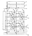
图1是本实施形态的OLED显示面板的构成图。在显示部分内矩阵状地配置具有作为象素发光体的OLED元件4的象素6。各个象素6通过写入线9、亮灯线10、信号线7、电源线8等连接到规定的外围驱动电路上。在这里,写入线9和亮灯线10被连接到象素选择电路11上,信号线7则通过信号输入开关13连接到模拟信号驱动电路12和时钟信号驱动电路16上,此外,还通过三角波输入开关14连接到三角波输入线15上。此外,象素6、象素选择电路11、模拟信号驱动电路12和数字信号驱动电路16,都用多晶Si-TFT在玻璃基板上形成。FIG. 1 is a configuration diagram of an OLED display panel according to the present embodiment.
在各个象素6中,信号线7通过存储电容1连接到驱动TFT2的栅极上,驱动TFT2的源极端子连接到电源线8上,驱动TFT2的漏极端子通过亮灯TFT5连接到OLED元件4上。此外,在驱动TFT2的栅极和漏极之间,设置复位TFT3,亮灯TFT5与复位TFT3的栅极分别连接到亮灯线10和写入线9上。在这里,驱动TFT2被构成为以OLED元件4为负载的反相器的一部分,复位TFT3可以看作是使上述反相器的输入输出短路的开关。In each
另外,至于多晶Si-TFT或OLED元件的制造方法,由于一般地说与已报道的方法没有什么大的不同,故在这里省略其说明。对于OLED元件4,例如可以参看先前说过的第1和第2现有例。In addition, as for the method of manufacturing a polycrystalline Si-TFT or an OLED element, generally speaking, there is no big difference from the reported method, so its description is omitted here. For the
此外,本实施形态中的象素选择电路11的构成,一般使用的是作为移位寄存器公知的电路构成,可以在一般的知识的范围内进行再构成。模拟信号驱动电路12虽然使用的是多晶Si-TFT面板中的一般的DA(数模)转换电路,但是除此之外也可以使用液晶驱动器LSI中的信号线驱动电路等。数字信号驱动电路16缓冲输出1位的输入数据,是并联缓冲电路。In addition, the configuration of the
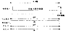
本实施形态,把1帧期间分成4个阶段进行动作。虽然实际上由分别由2个阶段构成的2个子帧构成,但是,在这里为了方便起见给这些阶段起一个从1/4帧到4/4帧的名字,按照顺序用图2和图3说明各个阶段中的动作。In the present embodiment, one frame period is divided into four stages to operate. Although it is actually composed of 2 subframes composed of 2 stages, here, for the sake of convenience, these stages are given a name from 1/4 frame to 4/4 frame, and are illustrated in Figure 2 and Figure 3 in order actions in each phase.
图2的(A)和(B)的时序图示出了构成帧前半子帧的1/4帧,和2/4帧的动作。在图2(A)的1/4帧期间中,用象素选择电路11依次扫描与各个象素行对应的写入线9和亮灯线10。在这里为了方便起见,在时序图中决定使上边表示‘ON’,使下边表示‘OFF’状态。这时信号输入开关13为ON,三角波输入开关14为OFF,象素选择电路11随着把象素行选择为A、B、C、…,通过信号线7,从模拟信号输出电路12向被选择的象素6写入模拟电压信号。在这里,由于已把模拟信号设定为5位,故具有32种信号电压电平。另外,写入线9、亮灯线10的附加字母A、B、C与各个象素行对应。在以下,也是同样的。The timing diagrams of (A) and (B) in FIG. 2 show operations of 1/4 frame and 2/4 frame constituting the first half of a frame. In the 1/4 frame period of FIG. 2(A), the writing line 9 and the
其次,在图2(B)的2/4帧期间中,归因于象素选择电路11,写入线9平常为OFF,亮灯线10则平常为ON。此外这时信号输入开关13为OFF,三角波输入开关14为ON。为此,通过三角波输入开关14和信号线7,从三角波输入线15,向全部象素输入图2(B)所示的那样的三角波形。Next, in the 2/4 frame period of FIG. 2(B), due to the
在这里,用图1更为详细地说明本子帧中的本实施形态的象素电路动作。如果在已给信号线7加上了某一模拟信号电压的状态下使复位TFT3和亮灯TFT5进行ON/OFF,则在向信号线7输入与之相同的模拟信号电压时,就把由驱动TFT2和OLED元件4构成的反相器的栅极电压变成反相器反转的阈值状态这样的状态,存储到存储电容1内。这就是1/4帧期间的模拟信号电压写入。接着,在2/4帧期间中,其动作是这样的:当向信号线7输入含有已写入的模拟信号电压值的三角波时,各个象素的反相器,在信号线7的电压比预先写入的模拟信号电压大的情况下,电流就不向OLED元件4流,而在比预先写入的模拟信号电压小的情况下,电流就向OLED元件4流。借助于此,可以借助于已写入的模拟信号电压来控制OLED的发光时间,同时,还可以消除起因于驱动TFT2的特性波动的反相器的反转阈值的波动。Here, the pixel circuit operation of this embodiment in this subframe will be described in more detail with reference to FIG. 1 . If the reset TFT3 and the lighting TFT5 are turned ON/OFF in the state where a certain analog signal voltage has been applied to the
下面,说明后半子帧。Next, the latter half of the subframes will be described.
图3的(A)和(B)的时序图示出了构成后半子帧的3/4帧和4/4帧的动作。图3(A)的3/4帧期间的动作,基本上也与1/4帧的动作是同样的。该情况下的动作与1/4帧的动作之间的差异在于:向信号线7输出的电压不是从模拟信号电压输出电路12,而是从数字信号电压输出电路16输出的数字电压。借助于此,随着象素选择电路11把象素行选择为A、B、C,通过信号线7从数字信号电压输出电路16向被选择的象素6写入相当于‘发光’或‘非发光’的两值中的任何一个的数字电压信号。The timing diagrams of (A) and (B) of FIG. 3 show operations of 3/4 frames and 4/4 frames constituting the second half of the subframes. The operation during the 3/4 frame period in FIG. 3(A) is basically the same as the operation during the 1/4 frame period. The difference between the operation in this case and the operation of 1/4 frame is that the voltage output to the
其次,在图3(B)的4/4帧期间中,归因于象素选择电路11,写入线9平常为OFF,亮灯线10平常为ON。此外,这时,虽然信号输入开关13为OFF,三角波输入开关14为ON,但是,该期间要通过三角波输入开关14和信号线7,从三角波输入线15向全部象素输入图3(B)所示的那样的数字信号电压的中间电压。Next, in the 4/4 frame period of FIG. 3(B), the writing line 9 is always OFF and the
在该情况下,各个象素的反相器电路(以下叫做象素反相器)的动作如下:在信号线7的中间电压比预先写入的数字信号电压大的情况下,电流就不向OLED元件4流,而在比预先写入的数字信号电压小的情况下,电流则向OLED元件4流。借助于此,就可以用已写入的数字信号电压决定各个OLED元件4的发光。另外,在这里由于象素反相器可以确实地选择ON或OFF状态,故也不会产生在控制象素反相器的反转时间的2/4帧中有可能产生的、起因于寄生效应的反转误差。就是说,在4/4帧中,可以期待极其正确的发光控制。结果是在本实施形态中,可以进行比仅仅用模拟信号电压驱动驱动全部的情况下,精度高2倍的发光控制。In this case, the operation of the inverter circuit of each pixel (hereinafter referred to as pixel inverter) is as follows: when the intermediate voltage of the
图4归纳示出了以上的OLED驱动顺序。另外,在图4还示出了1帧内的寻址期间Ts、模拟和数字灰度等级期间和与它们对应的OLED驱动的ON、OFF期间。帧期间,由前半和后半两个子帧构成,前半子帧由作为模拟信号电压寻址期间的1/4帧和作为模拟灰度等级发光期间的2/4帧构成,后半子帧由作为数字信号电压寻址期间的3/4帧和作为数字灰度等级发光期间的4/4帧构成。FIG. 4 generally shows the above OLED driving sequence. In addition, FIG. 4 also shows the addressing period Ts, analog and digital grayscale periods, and their corresponding ON and OFF periods of OLED driving within one frame. The frame period consists of the first half and the second half of two subframes. The first half of the subframe is composed of 1/4 frame as the analog signal voltage addressing period and 2/4 frame as the analog grayscale light emitting period. The second half of the subframe is composed of The 3/4 frame of the digital signal voltage addressing period is constituted by the 4/4 frame of the digital gray scale light emitting period.
在这里,模拟信号电压,表示全6位的数据中的除去MSB(最高位)之外的5位数据,数字信号电压则表示MSB数据。模拟灰度等级发光期间灰度等级显示,是发光/非发光的两值显示。另外,模拟灰度等级发光期间的最大发光(ON)期间,与数字灰度等级发光期间相等。Here, the analog signal voltage represents 5-bit data excluding the MSB (most significant bit) among all 6-bit data, and the digital signal voltage represents MSB data. The gray scale display during the simulated gray scale light emission is a two-value display of light emission/non-light emission. In addition, the maximum light-emitting (ON) period of the analog grayscale light-emitting period is equal to the digital grayscale light-emitting period.
在以上所述的本实施形态的例子中,在不偏离本发明的宗旨的范围内,可以有种种变更。例如,在本实施形态中,作为TFT基板虽然使用的是玻璃基板,但是,也可以把它变更为石英基板或透明塑料基板等别的透明绝缘基板。此外,只要把OLED元件4的发光取出到上表面上,则也可以使用不透明基板。In the examples of this embodiment described above, various changes can be made without departing from the gist of the present invention. For example, in this embodiment, a glass substrate is used as the TFT substrate, but it may be changed to another transparent insulating substrate such as a quartz substrate or a transparent plastic substrate. In addition, an opaque substrate may also be used as long as the light emitted by the
或者,对于各TFT,虽然在本实施形态中象素TFT使用的都是p沟道,但是,只要适宜变更驱动波形,也可以把它变更为n沟道或CMOS开关。对于象素反相器,也不限于由在这里使用的那样的驱动TFT2和OLED元件4构成的反相器,以CMOS反相器或使用n沟道TFT的恒流源电路位负载的构成,不言而喻也是可能的。Alternatively, although p-channel TFTs are used for the pixel TFTs in this embodiment, they can be changed to n-channel or CMOS switches as long as the driving waveform is changed as appropriate. For the pixel inverter, it is not limited to the inverter composed of the driving TFT2 and the
此外,在本实施形态的说明中,没有特意提到象素数和面板尺寸等。这是因为本发明并不特别限于这些规格或格式的发明。此外,虽然把显示信号电压作成64个灰度等级(6位),但是,比这更多的灰度等级也可以,反之,减少灰度等级也是容易的。就是说,作为由m位构成的2m灰度等级显示,在m位之内,只要从最高位(MSB)开始把k位用做两值的显示信号数据,(m-k)位就变成在模拟灰度等级显示中使用的信号,在本实施形态中,相当于m=6,k=1的情况。因此,可以根据需要的灰度等级变更m和k。In addition, in the description of this embodiment, the number of pixels, the panel size, etc. are not mentioned in particular. This is because the present invention is not particularly limited to inventions of these specifications or formats. In addition, although the display signal voltage is made into 64 gradation levels (6 bits), more gradation levels than this are possible, and conversely, it is easy to reduce the gradation levels. That is to say, as a 2 m grayscale display composed of m bits, within m bits, as long as k bits are used as two-valued display signal data starting from the most significant bit (MSB), the (mk) bits become in Signals used for analog grayscale display correspond to the case of m=6 and k=1 in this embodiment. Therefore, m and k can be changed according to the desired gray scale.
此外,在本实施形态中,由象素选择电路11、模拟信号驱动电路12、数字信号驱动电路16构成的外围驱动电路,用低温多晶Si-TFT电路构成。但是,在本发明的范围内,也可以用单晶LSI(大规模集成电路)构成并装配这些外围驱动电路或其一部分,反之,除此之外,三角波产生电路等也可以用低温多晶Si-TFT电路构成。In addition, in this embodiment, the peripheral driving circuit composed of the
在本实施形态中,作为发光元件使用OLED元件4。但是,显然,即便是不使用OLED元件4而代之以使用除此之外的含无机的一般的发光元件也会实现本发明。In this embodiment, an
以上的种种变更等并不限于本实施形态,在以下讲述的别的实施形态中,基本上也可以同样地应用。The above-mentioned various changes and the like are not limited to this embodiment, and can basically be applied in the same way to other embodiments described below.
<实施形态2><
其次,用图5和图6,对本发明的实施形态2进行说明。图5是本实施形态的OLED显示面板的构成图。在显示部分上,具有作为象素发光体的OLED元件24的象素25被配置成矩阵状。各个象素25,通过栅极线26、信号线27、电源线28等连接到外围的驱动电路上。Next,
在各象素25内,信号线27通过输入TFT21连接到驱动TFT23的栅极和存储电容22的一端上,驱动TFT23的一端和存储电容22的另一端共同连接到共用电源端子上。另一方面,栅极线26的一端连接到栅极扫描电路30上,信号线27的一端连接到模拟信号驱动电路29和数字信号驱动电路31上。另外,在这里,包括输入TFT21、驱动TFT23在内,用多晶Si-TFT,在玻璃基板上形成栅极扫描电路30、模拟信号驱动电路29和数字信号驱动电路31。In each
以下,说明本实施形态中的OLED显示面板的动作。在本实施形态中,帧由2个子帧构成。在这里,为了便于理解,假定把第1个子帧叫做1/2帧,把第2个子帧叫做2/2子帧进行以下的说明。Hereinafter, the operation of the OLED display panel in this embodiment will be described. In this embodiment, a frame is composed of two subframes. Here, for ease of understanding, it is assumed that the first subframe is called a 1/2 frame, and the second subframe is called a 2/2 subframe for the following description.
首先,在1/2帧的写入期间中,模拟信号驱动电路29因被激活而输出模拟信号电压,而数字信号驱动电路31因未被激活而使得输出阻抗变成为非常大。在这里,采用栅极扫描电路30通过栅极线26对规定的象素行的输入TFT21进行开闭扫描的办法,从模拟信号驱动电路29输入到信号线27上来的模拟信号电压,被输入至驱动TFT23的栅极和存储电容22,并保持一直到进行下一扫描写入为止的1个子帧期间。该期间,驱动TFT23向OLED元件24输入与上述模拟信号电压对应的模拟信号电流,借助于此,OLED元件24就以与上述模拟信号电压对应的模拟辉度进行发光。在这里,上述模拟信号电压是相当于5位的32个灰度等级的信号。First, in the writing period of 1/2 frame, the analog signal driving circuit 29 is activated to output an analog signal voltage, but the digital
其次,在2/2帧的写入期间中,数字信号驱动电路31因被激活而输出数字信号电压,而模拟信号驱动电路29因为未被激活而使得输出阻抗变成极大。在这里,采用栅极扫描电路30通过栅极线26对规定的象素行的输入TFT21进行开闭扫描的办法,从模拟信号驱动电路29输入到信号线27上来的模拟信号电压,被输入至驱动TFT23的栅极和存储电容22,并保持一直到进行下一扫描写入为止的1个子帧期间。该期间,驱动TFT23向OLED元件24输入与上述数字信号电压对应的数字信号电流,借助于此,OLED元件24就与上述数字信号电压对应地表示发光或非发光状态。在这里,上述数字信号是相当于MSB1位的ON或OFF的信号。Next, in the writing period of 2/2 frames, the digital
在本实施形态中,由于数字驱动时的OLED元件24可以确实地选择ON或OFF状态,故不会产生在模拟驱动时成为悬念的、起因于驱动TFT23中的阈值波动之类的特性波动的发光辉度误差。就是说,在2/2帧中,可以进行极其正确的发光控制。结果是在本实施形态中,可以进行比仅仅用模拟信号电压驱动驱动全部的情况下,精度高两倍的发光控制。In this embodiment, since the ON or OFF state of the
图6归纳示出了以上的驱动顺序。另外,图6还示出了与1帧内的扫描线扫描对应的模拟和数字灰度等级期间,和与之对应的第1行的OLED驱动辉度。帧期间由前半和后半两个子帧构成,前半子帧用作为模拟信号电压寻址期间的1/2帧,后半子帧是作为数字信号电压寻址期间的2/2帧构成。在这里,模拟信号电压,表示全6位的数据中的除去MSB(最高位)之外的5位数据,数字信号电压则表示MSB数据。模拟灰度等级发光期间的灰度等级显示,可以采用对发光辉度进行调制的办法进行控制,数字灰度等级发光期间的灰度等级,是发光/非发光的两值显示。另外,模拟灰度等级的发光期间被设定为与数字灰度等级发光期间相等的长度。FIG. 6 summarizes the above driving sequence. In addition, FIG. 6 also shows the analog and digital grayscale periods corresponding to the scanning lines in one frame, and the corresponding OLED driving luminance in the first row. The frame period is composed of two subframes, the first half and the second half, the first half subframe is used as 1/2 frame of the analog signal voltage addressing period, and the second half subframe is formed as 2/2 frame of the digital signal voltage addressing period. Here, the analog signal voltage represents 5-bit data excluding the MSB (most significant bit) among all 6-bit data, and the digital signal voltage represents MSB data. The grayscale display during the analog grayscale lighting period can be controlled by modulating the luminous brightness, and the grayscale level during the digital grayscale lighting period is a two-value display of luminous/non-luminous. In addition, the light-emitting period of the analog grayscale is set to have the same length as the light-emitting period of the digital grayscale.
本实施形态,模拟灰度等级发光时的辉度波动虽然变得比实施形态1比较大,但却具有象素构成简单的优点。This embodiment has the advantage that the pixel structure is simple although the fluctuation in luminance during pseudo-gradation light emission is larger than that of the first embodiment.
另外,人们知道在本实施形态那样的模拟信号电压驱动期间中,通过导入补偿抵消(自动归零)电路来抵消驱动TFT23的阈值电压波动的方法。这样的方法,例如,已在Technical digest of SID 98,pp.11-14(1998)(以下,叫做第3现有例)等中进行了讲述,但是在本实施形态中,采用使在该第3现有例中讲述的补偿抵消技术进行组合的办法,使得可以实现辉度波动更少的多灰度等级显示,或者,尽管使用特性波动更大的TFT却可以实现同样的高精度显示。In addition, it is known to introduce a compensation cancellation (auto-zero) circuit to cancel fluctuations in the threshold voltage of the driving
<实施形态3><
用图7和图8,对本发明的实施形态3进行说明。图7是本实施形态的液晶显示面板的构成图。具有作为光学特性调制元件的液晶电容33的象素34,在显示部分上被配置成矩阵状,象素34通过栅极线36、信号线35被连接到外围的驱动电路上。
在各象素34内,信号线35通过输入TFT 32被连接到液晶电容33的一端上,液晶电容33的另一端则连接到共用电源端子上。另一方面,栅极线36的一端连接到栅极扫描电路38上,信号线35的一端被连接到模拟信号驱动电路37和数字信号驱动电路39上。另外,在这里,包括输入TFT32在内,用多晶Si-TFT在玻璃基板上形成栅极扫描电路38、模拟信号驱动电路37和数字信号驱动电路39。此外,在本实施形态中,虽然显示面板在玻璃基板的背面上设置背光源,并形成为把液晶电容的相向电极和已形成了滤色片的相向玻璃基板等组合起来,但是,它们的构造是极其普通的构造,故在这里省略其详细的说明。In each
以下,说明本实施形态的动作。在本实施形态中,帧由3个子帧构成。在这里,为了便于理解起见,假定把第1个子帧叫做1/3帧,把第2个子帧叫做2/3帧,把第3个子帧叫做3/3帧,进行以下的说明。The operation of this embodiment will be described below. In this embodiment, a frame is composed of three subframes. Here, for ease of understanding, it is assumed that the first subframe is called a 1/3 frame, the second subframe is called a 2/3 frame, and the third subframe is called a 3/3 frame, and the following description will be given.
首先,在1/3帧的写入期间中,模拟信号驱动电路37因被激活而输出模拟信号电压,而数字信号驱动电路39因未被激活而使得输出阻抗变成非常大。在这里,采用栅极扫描电路38通过栅极线36对规定的象素行的输入TFT32进行开闭扫描的办法,从模拟信号驱动电路37输入到信号线35上的模拟信号电压,被输入至液晶电容33,并保持一直到进行下一扫描写入为止的1个子帧期间。该期间,液晶电容33给液晶层加上相当于所写入的模拟信号电压的模拟信号电场,液晶层产生规定的光学特性调制效应。在这里,上述模拟信号电压是相当于4位的16个灰度等级的信号。First, in the writing period of 1/3 frame, the analog
其次,在2/3帧的写入期间中,数字信号驱动电路39因被激活而输出模拟信号电压,而模拟信号驱动电路37因未被激活而使得输出阻抗变成为非常大。在这里,再次采用通过栅极线36栅极扫描电路38对规定的象素行的输入TFT21进行开闭扫描的办法,从数字信号驱动电路39输入到信号线35上的数字信号电压,被输入至液晶电容33,并保持一直到进行其后的扫描写入为止的1个子帧期间。该期间,液晶电容33给液晶层加上相当于上所写入的数字信号电压的数字信号电场,借助于此,液晶层就与上述数字信号对应地表示光学性地透过或非透过状态。在这里,上述数字信号,是相当于MSB1位的ON或OFF的信号。Next, in the writing period of 2/3 frames, the digital signal driving circuit 39 is activated to output an analog signal voltage, but the analog
其次,在3/3帧的写入期间中,数字信号驱动电路39也因被激活输出模拟信号电压,而模拟信号驱动电路37也因未被激活而使得输出阻抗变成为非常大。在这里,再次采用通过栅极线36栅极扫描电路38对规定的象素行的输入TFT21进行开闭扫描的办法,从数字信号驱动电路39输入到信号线35上的数字信号电压,被输入至液晶电容33,并保持一直到进行其后的扫描写入为止的1个子帧期间。该期间,液晶电容33给液晶层加上相当于上所写入的数字信号电压的数字信号电场,借助于此,液晶层就与上述数字信号对应地表示光学性地透过或非透过状态。在这里,上述数字信号,是相当于MSB1位的ON或OFF的信号。Next, in the writing period of 3/3 frame, the digital signal driving circuit 39 is also activated to output an analog signal voltage, and the analog
在本实施形态中,在作为数字驱动的2/3和3/3帧时的液晶电容33,也由于可以确实地选择ON或OFF状态,而使得不会产生在模拟驱动时成为悬念那样的、起因于驱动TFT32的场穿通电荷的调制辉度误差。就是说,在2/3帧和3/3帧中,可以进行极其正确的发光控制。结果,在本实施形态中,可以进行比仅仅用模拟信号电压驱动驱动全部的情况下,精度高4倍的发光控制。In the present embodiment, the
图8归纳示出了以上的驱动顺序。另外,图8还示出了与1帧内的扫描线扫描对应的模拟和数字灰度等级期间,和与之对应的第1行的象素辉度。帧期间由3个子帧构成,第1个子帧用作为模拟信号电压寻址期间的1/3帧,后半的2个子帧由作为数字信号电压寻址期间的2/3和3/3帧构成。在这里,模拟信号电压表示全6位的数据内的从MSB开始除去2位的4位数据,数字信号电压表示MSB和下1位数据。FIG. 8 summarizes the above driving sequence. In addition, FIG. 8 also shows the analog and digital grayscale periods corresponding to the scanning lines in one frame, and the corresponding pixel luminance of the first line. The frame period is composed of 3 subframes, the first subframe is used as 1/3 frame during the analog signal voltage addressing period, and the second half of the 2 subframes is composed of 2/3 and 3/3 frames during the digital signal voltage addressing period . Here, the analog signal voltage represents 4-bit data excluding 2 bits from the MSB in all 6-bit data, and the digital signal voltage represents the MSB and next 1-bit data.
模拟灰度等级发光期间的灰度等级显示,可以采用对发光辉度进行调制的办法进行控制,数字灰度等级发光期间的灰度等级,是发光/非发光的两值显示。另外,作为1/3帧的模拟灰度等级期间,被设定为比作为3/3帧的数字灰度等级发光期间2的长度相等,这相当于作为2/3帧的数字灰度等级期间1的一半。The grayscale display during the analog grayscale lighting period can be controlled by modulating the luminous brightness, and the grayscale level during the digital grayscale lighting period is a two-value display of luminous/non-luminous. In addition, the analog grayscale period that is 1/3 frame is set to be equal in length to the digital grayscale
在这里,之所以把相当于最高位的灰度等级显示作成3个子帧中在时间上位于中间的2/3帧,理由如下。就是说,人们知道,如果发光(透过)期间的时间轴重心随着显示灰度等级而变动,则就会产生模拟轮廓这样的伪信号。为了缓和这一现象,于是就把发光期间最长的最高位的位配置到帧的中心附近。Here, the reason why the gradation corresponding to the highest bit is displayed as the temporally middle 2/3 frame among the three subframes is as follows. That is, it is known that if the center of gravity of the time axis during the light emission (transmission) period changes with the display gray scale, false signals such as analog contours will be generated. In order to alleviate this phenomenon, the most significant bit with the longest light-emitting period is arranged near the center of the frame.
另外,在本实施形态中,虽然把模拟信号定为4位,把数字信号定为2位,这些位数可以根据所求的规格适当进行变更,数字信号位数大的一方灰度等级精度会提高,但是相反,帧数的增加却会招致面板驱动频率的增大,所以,理想的是选择与用途相对应的位数。此外,在本实施形态那样的液晶面板的情况下,一般由于存在着应答速度的问题,故对于子帧的增加,存在着液晶层应答速度上的界限。In addition, in this embodiment, although the analog signal is set to 4 bits, and the digital signal is set to 2 bits, these bits can be appropriately changed according to the required specifications. However, on the contrary, an increase in the number of frames will lead to an increase in the drive frequency of the panel, so it is ideal to select the number of bits corresponding to the purpose. In addition, in the case of a liquid crystal panel as in this embodiment, there is generally a problem with the response speed, so there is a limit in the response speed of the liquid crystal layer with respect to the increase of sub-frames.
此外,数字信号的位数的变更,并不限于本实施形态这样的液晶显示面板,前边所说的实施形态1、2那样的发光显示面板,当然也是可能的。In addition, the change of the number of digits of the digital signal is not limited to the liquid crystal display panel of this embodiment, and of course it is also possible for the light-emitting display panels of the first and second embodiments mentioned above.
<实施形态4><
用图9-图12,对本发明的实施形态4进行说明。首先,用图9说明本实施形态的全体构成。
图9是本实施形态的OLED显示面板的构成图。具有作为象素发光体的OLED44的象素47在显示部分上被配置成矩阵状。象素47通过写入线50、复位线52、显示线51、信号线48、电源线49等被连接到规定的外围驱动电路上。在这里,写入线50、复位线52和显示线51被连接到象素选择电路53上,信号线48则被连接到模拟信号驱动电路54和数字信号驱动电路55上。此外,象素47,象素选择电路53、模拟信号驱动电路54和数字信号驱动电路55全都用多晶Si-TFT在玻璃基板上形成。FIG. 9 is a configuration diagram of an OLED display panel according to this embodiment.
在各个象素47内,信号线48通过输入TFT41和存储电容42连接到驱动TFT46的栅极上,驱动TFT46的源极端子则连接到输入TFT41和显示TFT45的一端上。在这里,显示TFT45的多端连接到电源线49上。驱动TFT46的漏极端子则连接到OLED44上。此外,驱动TFT46的漏极端子和栅极端子之间设置有复位TFT43,输入TFT41、复位TFT43、显示TFT45的栅极分别连接到写入线50、复位线52、显示线45上。In each
在这里,模拟信号驱动电路54和数字信号驱动电路55的基本作用,虽然与实施形态1中的模拟信号驱动电路12和数字信号驱动电路16是同样的,但在本实施形态中不同的是输出信号是电流而不是电压。为此,在本实施形态中,在模拟信号驱动电路54和数字信号驱动电路55的信号输出部分中使用进行电流源连接的TFT。Here, although the basic functions of the analog
本实施形态,把1帧期间分成4个阶段进行动作。实际上,虽然分别由2个阶段构成2个子帧,但是在这里为了便于理解,赋予这些阶段从1/4帧到4/4帧的名字,用图10和图11按照顺序说明各个阶段中的动作。In the present embodiment, one frame period is divided into four stages to operate. In fact, although two subframes are composed of two stages, for the sake of easy understanding, these stages are given names from 1/4 frame to 4/4 frame, and Figures 10 and 11 are used to illustrate the steps in each stage in order. action.
图10的时序图示出了构成帧的前半子帧的1/4帧的动作。在1/4帧期间中,用象素选择电路53依次扫描与各个象素行对应的写入线50和复位线52。该期间,显示线51平常是OFF状态。随着象素选择电路53把象素行选择为A、B、C…,通过信号线48从模拟信号驱动电路54向被选择的象素47写入模拟信号电流。在这里,模拟信号由于被设计为5位,故具有32种信号电流电平。接着,在2/4帧期间(未画出来)采用使显示线51变成为ON的办法,向各个象素供给发光电力。The timing chart of FIG. 10 shows the operation of 1/4 frame which constitutes the first half of the subframe of a frame. In a 1/4 frame period, the
在这里,用图9更详细地说明本子帧中的象素电路动作。当在已向信号线48加上了模拟信号电流的状态下使输入TFT和复位TFT43变成ON/OFF时,通过驱动TFT46向OLED元件44流动正在向信号线49输入的同一信号电流。这时的驱动TFT46的栅极-源极间电压,由于已连接到存储电容42的两端上,故在复位TFT43变成OFF的时刻处,该栅极-源极间电压条件就被存储在存储电容42的两端。这就是在1/4帧期间的模拟信号电流写入。Here, the operation of the pixel circuit in this subframe will be described in more detail with reference to FIG. 9 . When the input TFT and the
接着,在2/4帧期间中,显示线52变成ON。借助于此,驱动TFT46虽然会再次变成为ON,但是,由于这时向驱动TFT46流的电流量由已预先存储在存储电容42中的栅极-源极间电压条件决定,故与在帧1/4处输入到象素内的模拟信号电流值相等。因此,OLED元件44的驱动电流受所写入的模拟信号电流控制,也可以同时控制发光电流量。Next, during the 2/4 frame period, the
其次,说明后半子帧。图11的时序图示出了构成后半子帧的3/4帧的动作。3/4帧期间的动作,基本上也与1/4帧的动作是同样的,在该情况下与1/4帧的动作之间的差异在于供往信号线48的电流不是从模拟信号电流驱动电路54,而是从数字信号驱动电路55输出的数字电流。借助于此,随着象素选择电路53把象素行选择为A、B、C、…,就通过信号线48,从数字信号驱动电路55向被选择的象素47写入相当于‘发光’或‘非发光’的两值中的任何一个数字电流信号,接着,在4/4帧期间(未画出来)采用使显示线51再次变成ON的办法,向各个象素供给发光电力。Next, the latter half of the subframes will be described. The timing chart in FIG. 11 shows the operation of 3/4 frames constituting the second half of the subframes. The operation during the 3/4 frame is basically the same as the operation of the 1/4 frame. In this case, the difference from the operation of the 1/4 frame is that the current supplied to the
图12归纳示出了以上的驱动顺序。另外,图12示出了1帧之内的寻址期间Ts、模拟和数字灰度等级期间和与它们对应的OLED驱动和显示线51的ON、OFF期间。帧期间由前半和后半2个子帧构成。前半子帧由作为模拟信号电流寻址期间的1/4帧,和作为模拟灰度等级发光期间的2/4帧构成;后半子帧由作为数字信号电流寻址期间的3/4帧,和作为数字灰度等级发光期间的4/4帧构成。在这里,模拟信号电流显示除去全6位数据中的LSB(最低位)之外的5位数据,数字信号电压显示LSB数据。模拟灰度等级发光期间的灰度等级显示,采用对发光时间进行调制的办法被控制为32个值,数字灰度等级发光期间的灰度等级,是发光/非发光两值显示。另外,数字灰度等级发光期间,是模拟灰度等级发光期间的1/64的期间。FIG. 12 summarizes the above driving sequence. In addition, FIG. 12 shows the addressing period Ts, the analog and digital grayscale periods, and the ON and OFF periods of the OLED driving and
在这里,本实施形态中的象素47内的电路构成本身是已知的技术,详细情况已在Technical digest of International Electron DeviceMeeting 98,pp.875-878(1998)(以下,叫做第4现有例)等中讲述。在该第4现有例的情况下,发光辉度仅仅用模拟信号电流进行灰度等级控制。但是,在该第4现有例中,存在着当模拟信号电流的值变小时,就不能向象素正确地写入信号电流的问题。这是因为在模拟信号电流的值小的情况下,信号线的寄生电容的充放电就要花费时间,现实上在可进行动画显示的帧速率的情况下,就不能进行图象信号的写入了。Here, the circuit configuration itself in the
例如,即便是假定为是2英寸左右的OLED面板的情况下,即便是在通常的设计中,把与写入线或象素之间的寄生电容估计得小,在信号线上也会产生4pF左右。在这里,假定最小信号电流值为2nA,假定写入电压为1V,则上述寄生电容的充放电也需要200微秒,如果是每秒60帧,则必须把最大象素行数作成83行。For example, even if the OLED panel is assumed to be about 2 inches, even in a normal design, if the parasitic capacitance between the writing line or the pixel is estimated to be small, 4pF will be generated on the signal line about. Here, assuming that the minimum signal current value is 2nA and the writing voltage is 1V, it takes 200 microseconds to charge and discharge the above-mentioned parasitic capacitance. If it is 60 frames per second, the maximum number of pixel rows must be set to 83 rows.
相对于此,在本实施形态的情况下,由于最低位的位即最小位(LSB)以数字电流信号进行输入,故信号电流值与模拟信号电流值的最大值是相同的。因此,必须以实质上最小信号电流值写入的是从LSB开始的第2位,所以如果是上述的数值,则最小电流值为40nA。归因于此,在本实施形态的情况下,在同一条件下也可以使最大象素行增加到166行。On the other hand, in this embodiment, since the least significant bit (LSB) which is the lowest bit is input as a digital current signal, the maximum value of the signal current value and the analog signal current value are the same. Therefore, it is the second bit from the LSB that must be written with substantially the minimum signal current value, so if it is the above-mentioned value, the minimum current value is 40nA. Due to this, in the case of the present embodiment, the maximum number of pixel lines can be increased to 166 under the same conditions.
在本实施形态中虽然仅仅把数字灰度等级应用于LSB,但是,如果把数字灰度等级应用于从LSB开始的多位,则也可以实现更多象素、大型或更多灰度等级的显示面板。就是说,如果假定作为由m位得到的2m灰度等级显示,把m位中的从最低位(LSB)开始的n位作为两值的显示信号数据,则(m-n)位就进行DA转换变成为在模拟多值灰度等级显示中使用的信号,在本实施形态中,相当于m=6,n=1的情况。因此只要根据需要的灰度等级变更该m和n即可。但是,在把n取得大的情况下,必须注意会伴随有子帧数的增加这一点。In this embodiment, although the digital gray scale is only applied to the LSB, if the digital gray scale is applied to multiple bits starting from the LSB, it is also possible to realize more pixels, large or more gray scales. display panel. That is to say, if it is assumed that 2m grayscale display obtained by m bits is used, and n bits starting from the lowest bit (LSB) of m bits are used as two-valued display signal data, then (mn) bits are subjected to DA conversion. This becomes a signal used for analog multi-level grayscale display, and corresponds to the case of m=6 and n=1 in this embodiment. Therefore, it is only necessary to change the m and n according to the required gray scale. However, when n is made large, attention must be paid to the fact that the number of subframes is accompanied by an increase.
<实施形态5><
用图13和图14对本发明的实施形态5进行说明。首先,用图13对本实施形态的全体构成进行说明。
图13是作为本实施形态的OLED显示面板的构成图。具有作为象素发光体的OLED44的象素47在显示部分上被配置成矩阵状。各个象素47都通过写入线50、复位线52、显示线51、信号线48、电源线49等被连接到规定的外围驱动电路上。在这里,写入线50、复位线52和显示线51被连接到象素选择电路53上,信号线48则被连接到多值信号驱动电路60上。此外,象素47、象素选择电路53、多值信号驱动电路60全都用多晶Si-TFT在玻璃基板上形成。在各个象素47内,信号线48通过输入TFT41和存储电容42连接到驱动TFT46的栅极上,驱动TFT46的源极端子则连接到输入TFT41和显示TFT45的一端上。FIG. 13 is a configuration diagram of an OLED display panel according to this embodiment.
在这里,显示TFT45的多端连接到电源线49上。驱动TFT46的漏极端子则连接到OLED元件44上。此外,驱动TFT46的漏极端子和栅极端子之间设置有复位TFT43,输入TFT41、复位TFT43、显示TFT45的栅极,分别连接到写入线50、复位线52、显示线45上。Here, multiple terminals of
在这里,多值信号驱动电路60的基本作用,是输出多值的信号电流,对于一般熟知的多值信号电压输出电路,向信号输出部分附加上了进行电流源连接的TFT。Here, the basic function of the multi-valued
本实施形态把1帧期间分成4个阶段进行动作。虽然实际上由分别由2个阶段构成的2个帧构成,但是,在这里为了方便起见给这些阶段起一个从1/4帧到4/4帧的名字。本实施形态中的动作,要加到信号线48上的信号电流的大小,除去1/4帧和3/4帧包括0在内都是8个灰度等级这一点之外,与已经用图10和图11说明的实施形态4中的动作是同样的,故在此省略除此之外的说明。In this embodiment, one frame period is divided into four stages to operate. Although it actually consists of two frames each consisting of two stages, these stages are given names from 1/4 frame to 4/4 frame here for convenience. The action in this embodiment, the size of the signal current to be added to the
图14归纳示出了本实施形态的驱动顺序。另外,图14还示出了1帧内的、寻址期间Ts和时间权数为8的高位的位数字灰度等级期间和时间权数为1的低位的位数字灰度等级期间和8个灰度等级显示OLED驱动和信号线51的ON/OFF期间。Fig. 14 schematically shows the driving sequence of this embodiment. In addition, FIG. 14 also shows the address period Ts and the high bit digital gray scale period with a time weight of 8, the low bit digital gray scale period with a time weight of 1, and the 8 bit digital gray scale periods within one frame. Gray scales show ON/OFF periods of the OLED drive and
帧期间由前半和后半两个子帧构成,前半子帧的高位的3位的数据和后半子帧的低位的3位的数据,分别用8个灰度等级的OLED元件44的发光辉度表现。在这里,前半子帧,由作为高位的3位的多值信号电流寻址期间的1/4帧,和作为高位的3位的多灰度等级发光期间的2/4帧构成;后半子帧由作为低位的3位的多值信号电流寻址期间的3/4帧,和作为低位的3位的多灰度等级发光期间的4/4帧构成。The frame period is composed of two subframes, the first half and the second half, and the high-order 3-bit data of the first-half subframe and the low-order 3-bit data of the second half subframe use the luminous luminance of the
在这里,前半子帧可以看作是8进制2位数据中的高位显示,后半子帧则可以看作是8进制2位数据中的低位显示。因此,把相当于8进制的8倍的时间权数赋予2/4帧和4/4帧的发光期间。Here, the first half of the subframes can be regarded as the high-order display in the 2-bit octal data, and the second half of the sub-frames can be regarded as the low-order display in the 2-bit octal data. Therefore, a time weight equivalent to eight times the octal system is given to the light-emitting periods of the 2/4 frame and the 4/4 frame.
在本实施形态中,也具有可以把多值信号电流的最小写入电流值取得大的优点,具有可以向象素写入正确的信号电流的优点。这是因为如果仅仅是通常的模拟信号电流,则需要64个灰度等级的信号电流写入,而在本实施形态的情况下,只需8个灰度等级信号电流写入即可。Also in this embodiment, there is an advantage that the minimum write current value of the multi-valued signal current can be made large, and there is an advantage that an accurate signal current can be written to the pixel. This is because it is necessary to write signal currents for 64 gradation levels if only normal analog signal currents are used, but only 8 gradation level signal currents are required for writing in the present embodiment.
另外,在本实施形态的情况下,虽然实现了用8进制8位得到的64个灰度等级的显示,但是并不特别限于上述值。若采用另外的表现,则可以是x进制y位的组合。例如,人们认为同样是实现64个灰度等级,可以采用4进制3位,而256个灰度等级的实现,可以采用4进制4位。In addition, in the case of the present embodiment, although the display of 64 gradation levels obtained by 8 bits in octal is realized, it is not particularly limited to the above-mentioned values. If another expression is adopted, it may be a combination of x-ary and y-digit. For example, it is believed that to realize 64 gray levels, 3 bits in 4-ary system can be used, and 256 gray-scale levels can be realized, and 4 bits in 4-ary system can be used.
此外,也没有必要把x进制y位的组合全部都用在灰度等级显示上。例如,也可以借助于在64个灰度等级的显示中采用5进制3位的办法,对64个灰度等级加以非线性灰度系数修正的、或仅仅使最大辉度灰度等级极端地突出,实现所谓的峰值辉度产生那样的非线性辉度显示。In addition, it is not necessary to use all combinations of x-ary and y-bits for grayscale display. For example, it is also possible to apply nonlinear gamma correction to the 64 gray levels, or only make the maximum luminance gray level extreme It stands out and realizes a nonlinear luminance display such as so-called peak luminance generation.
或者,也可以借助于R、G、B的显示色,变更要使用的信号电流级。Alternatively, the signal current level to be used may be changed by displaying colors of R, G, and B.
由于本实施形态是x进制数字驱动的概念,由于可能会被看作是偏离了作为本发明的构思的‘模拟信号’和‘数字信号’的并用这一概念,所以为了慎重起见,在这里再加以说明。现有的图象显示装置中的‘数字信号’的定义,很明显是‘2进制字信号’,其值只能选取ON或OFF这两个值。与此不同,本发明是在同一个装置上并用‘选取多值的模拟信号’的概念。就是说,在本发明中定义的‘模拟信号’没有必要非是连续的无限灰度等级不可,而是‘多值信号’,这也包括‘x进制字信号’。本实施形态的概念是一种在子帧这一数字化的概念中存在着‘多值信号’这样的思考方法,所以就是本发明的思考方法。另外,由以上的讨论可知,不言而喻,本发明的概念中含有在使用‘子帧’的同时在每一个子帧中仅仅显示‘模拟信号’这样的概念。Since this embodiment is the concept of x-ary digital drive, it may be regarded as deviating from the concept of the combined use of 'analog signal' and 'digital signal' as the concept of the present invention, so for the sake of caution, here Let me explain. The definition of 'digital signal' in the existing image display device is obviously 'binary word signal', and its value can only select these two values of ON or OFF. Different from this, the present invention uses the concept of 'selecting multi-valued analog signals' together on the same device. That is to say, the 'analog signal' defined in the present invention does not necessarily have to be a continuous infinite gray scale, but a 'multi-valued signal', which also includes 'x-ary word signal'. The concept of this embodiment is a way of thinking that a 'multi-valued signal' exists in the digitized concept of a subframe, and thus is the way of thinking of the present invention. In addition, from the above discussion, it goes without saying that the concept of the present invention includes the concept of displaying only 'analog signal' in each subframe while using 'subframe'.
<实施形态6><
用图15对本发明的实施形态6进行说明。图15是作为本实施形态的个人数字助理(PDA)100的构成图。
在无线接口(I/F)电路102中,作为以近距离无线存取系统的规格为基础的无线数据,从外部输入压缩图象数据等。无线I/F电路102的输出,通过I/O电路103连接到数据总线108上。在数据总线108上,除此之外,还连接有微处理器(MPU)104、显示面板控制器106和帧存储器107。In the wireless interface (I/F)
此外,显示面板控制器106的输出,输入至OLED显示面板101。另外,在个人数字助理100中,还设置有三角波产生电路105和电源109,三角波产生电路105的输出输入至OLED显示面板101。在这里,OLED显示面板101由于具有与先前所说的实施形态1同样的构成和动作,故在这里省略其内部的构成和动作的叙述。In addition, the output of the
说明本实施形态的动作。首先,无线I/F电路102根据指令从外部取入压缩图象数据,通过I/O电路103把该图象数据传送给微处理器104和帧存储器107。微处理器104接受来自使用者的指令操作,根据需要驱动个人数字助理100全体,进行压缩图象数据的译码或信号处理。信号处理后的图象数据,暂时存储在帧存储器107内。The operation of this embodiment will be described. First, the wireless I/
在这里,在微处理器104发出了显示指令的情况下,就根据该指令通过显示面板控制器106从帧存储器107向OLED显示面板101输入图象数据,OLED显示面板101就实时地显示所输入的图象数据。这时显示面板控制器106输出为了同时显示图象所必须的定时脉冲,三角波产生电路105与之同步地输出三角波形状的图象驱动电压。Here, when the microprocessor 104 issues a display instruction, the image data is input from the
另外,OLED显示面板101用这些信号实时地显示由6位的图象数据产生的显示数据,对于这一点与实施形态1所述的情况是同样的。在这里,在电源109中含有二次电池,供给驱动这些个人数字助理100全体的电力。In addition, the
倘采用本实施形态,则可以提供可进行高精度的多灰度等级显示的个人数字助理100。According to this embodiment, the personal
另外,在本实施形态中,作为图象显示元件使用的是在实施形态1中说明的OLED显示面板,但是除此之外,显然还可以使用本发明的其它实施形态中说明的种种显示面板。In this embodiment, the OLED display panel described in
由前边所说的实施形态可知,倘采用本发明,则可以得到消除了微小噪声或驱动频率的高速化的问题的、可进行多灰度等级的高精度显示的图象显示装置。As can be seen from the above-mentioned embodiments, according to the present invention, an image display device capable of multi-gray scale high-precision display can be obtained that eliminates the problems of minute noise and high-speed driving frequency.
Claims (21)
Applications Claiming Priority (2)
| Application Number | Priority Date | Filing Date | Title |
|---|---|---|---|
| JP2002142469A JP2003330422A (en) | 2002-05-17 | 2002-05-17 | Image display device |
| JP142469/2002 | 2002-05-17 |
Publications (2)
| Publication Number | Publication Date |
|---|---|
| CN1514426A CN1514426A (en) | 2004-07-21 |
| CN100399390C true CN100399390C (en) | 2008-07-02 |
Family
ID=29417003
Family Applications (1)
| Application Number | Title | Priority Date | Filing Date |
|---|---|---|---|
| CNB021559864A Expired - Lifetime CN100399390C (en) | 2002-05-17 | 2002-12-12 | image display device |
Country Status (5)
| Country | Link |
|---|---|
| US (1) | US7286105B2 (en) |
| JP (1) | JP2003330422A (en) |
| KR (1) | KR20030089404A (en) |
| CN (1) | CN100399390C (en) |
| TW (1) | TW594639B (en) |
Families Citing this family (68)
| Publication number | Priority date | Publication date | Assignee | Title |
|---|---|---|---|---|
| GB0218172D0 (en) * | 2002-08-06 | 2002-09-11 | Koninkl Philips Electronics Nv | Electroluminescent display device |
| JP2004157250A (en) | 2002-11-05 | 2004-06-03 | Hitachi Ltd | Display device |
| JP2004341144A (en) * | 2003-05-15 | 2004-12-02 | Hitachi Ltd | Image display device |
| JP2005099713A (en) * | 2003-08-25 | 2005-04-14 | Seiko Epson Corp | Electro-optical device, driving method of electro-optical device, and electronic apparatus |
| US7126566B2 (en) * | 2003-11-01 | 2006-10-24 | Wintek Corporation | Driving circuit and driving method of active matrix organic electro-luminescence display |
| JP5051565B2 (en) * | 2003-12-10 | 2012-10-17 | 奇美電子股▲ふん▼有限公司 | Image display device |
| KR100560446B1 (en) * | 2004-03-15 | 2006-03-13 | 삼성에스디아이 주식회사 | Light emitting display device and driving method thereof |
| KR100560445B1 (en) * | 2004-03-15 | 2006-03-13 | 삼성에스디아이 주식회사 | Light emitting display device and driving method thereof |
| US20050243032A1 (en) * | 2004-04-29 | 2005-11-03 | Kuo-Sheng Lee | Power line layout for electroluminescent display |
| US7023449B2 (en) * | 2004-04-30 | 2006-04-04 | Hewlett-Packard Development Company, L.P. | Displaying least significant color image bit-planes in less than all image sub-frame locations |
| JP5087820B2 (en) * | 2004-05-25 | 2012-12-05 | 株式会社Jvcケンウッド | Display device |
| JP4843914B2 (en) * | 2004-07-07 | 2011-12-21 | セイコーエプソン株式会社 | Electro-optical device, driving method thereof, and electronic apparatus |
| KR100624311B1 (en) * | 2004-08-30 | 2006-09-19 | 삼성에스디아이 주식회사 | Frame memory control method and display device using same |
| JP4846998B2 (en) * | 2004-10-08 | 2011-12-28 | 株式会社 日立ディスプレイズ | Image display device |
| JP4403401B2 (en) * | 2004-10-13 | 2010-01-27 | ソニー株式会社 | Information processing apparatus and method, recording medium, and program |
| JP4846999B2 (en) * | 2004-10-20 | 2011-12-28 | 株式会社 日立ディスプレイズ | Image display device |
| KR100688799B1 (en) * | 2004-11-17 | 2007-03-02 | 삼성에스디아이 주식회사 | Light emitting display, driving method and driving method of pixel circuit |
| JP4437110B2 (en) | 2004-11-17 | 2010-03-24 | 三星モバイルディスプレイ株式會社 | Organic light emitting display device, driving method of organic light emitting display device, and driving method of pixel circuit |
| JP5264014B2 (en) * | 2004-11-30 | 2013-08-14 | 株式会社半導体エネルギー研究所 | Semiconductor device, display device and electronic apparatus |
| WO2006059737A1 (en) * | 2004-11-30 | 2006-06-08 | Semiconductor Energy Laboratory Co., Ltd. | Display device and driving method thereof, semiconductor device, and electronic apparatus |
| US7502040B2 (en) * | 2004-12-06 | 2009-03-10 | Semiconductor Energy Laboratory Co., Ltd. | Display device, driving method thereof and electronic appliance |
| US7515149B2 (en) * | 2004-12-17 | 2009-04-07 | Eastman Kodak Company | Display with wirelessly controlled illumination |
| US7646367B2 (en) * | 2005-01-21 | 2010-01-12 | Semiconductor Energy Laboratory Co., Ltd. | Semiconductor device, display device and electronic apparatus |
| US8681077B2 (en) | 2005-03-18 | 2014-03-25 | Semiconductor Energy Laboratory Co., Ltd. | Semiconductor device, and display device, driving method and electronic apparatus thereof |
| CN102394049B (en) * | 2005-05-02 | 2015-04-15 | 株式会社半导体能源研究所 | Driving method of display device |
| EP1720149A3 (en) * | 2005-05-02 | 2007-06-27 | Semiconductor Energy Laboratory Co., Ltd. | Display device |
| US8059109B2 (en) | 2005-05-20 | 2011-11-15 | Semiconductor Energy Laboratory Co., Ltd. | Display device and electronic apparatus |
| US7683913B2 (en) * | 2005-08-22 | 2010-03-23 | Semiconductor Energy Laboratory Co., Ltd. | Display device and driving method thereof |
| KR101324756B1 (en) | 2005-10-18 | 2013-11-05 | 가부시키가이샤 한도오따이 에네루기 켄큐쇼 | Display device and driving method thereof |
| KR100662998B1 (en) | 2005-11-04 | 2006-12-28 | 삼성에스디아이 주식회사 | Organic electroluminescent display and its driving method |
| GB2436391B (en) | 2006-03-23 | 2011-03-16 | Cambridge Display Tech Ltd | Image processing systems |
| EP2924498A1 (en) | 2006-04-06 | 2015-09-30 | Semiconductor Energy Laboratory Co, Ltd. | Liquid crystal desplay device, semiconductor device, and electronic appliance |
| JP2007323036A (en) * | 2006-06-05 | 2007-12-13 | Samsung Sdi Co Ltd | Organic electroluminescent display device and driving method thereof |
| TWI391890B (en) * | 2006-10-11 | 2013-04-01 | Japan Display West Inc | Display apparatus |
| US7928939B2 (en) * | 2007-02-22 | 2011-04-19 | Apple Inc. | Display system |
| JP2008292649A (en) | 2007-05-23 | 2008-12-04 | Hitachi Displays Ltd | Image display device |
| KR100789654B1 (en) * | 2007-08-20 | 2008-01-02 | 주식회사 티엘아이 | Mixing pixel driving method in active display device |
| JP5327774B2 (en) * | 2007-11-09 | 2013-10-30 | グローバル・オーエルイーディー・テクノロジー・リミテッド・ライアビリティ・カンパニー | Display device |
| KR101409539B1 (en) * | 2007-12-18 | 2014-07-03 | 엘지디스플레이 주식회사 | Organic electroluminescence display device and driving method thereof |
| WO2009082056A1 (en) * | 2007-12-24 | 2009-07-02 | Syncoam Co., Ltd | Hybrid driving device and method of amoled panel using multi-analog gradation current |
| JP5236324B2 (en) | 2008-03-19 | 2013-07-17 | グローバル・オーエルイーディー・テクノロジー・リミテッド・ライアビリティ・カンパニー | Display panel |
| JP2009244666A (en) * | 2008-03-31 | 2009-10-22 | Sony Corp | Panel and driving controlling method |
| CN101620817B (en) * | 2008-07-02 | 2011-09-28 | 联咏科技股份有限公司 | Driving method for a flat panel display and related driving device |
| JP2010054989A (en) * | 2008-08-29 | 2010-03-11 | Mitsubishi Electric Corp | Gradation control method and display device |
| JP2010078807A (en) * | 2008-09-25 | 2010-04-08 | Canon Inc | Active matrix type display device, method of manufacturing the same, and method of driving the same |
| JP2009294676A (en) * | 2009-09-17 | 2009-12-17 | Hitachi Ltd | Display device |
| JP2011150004A (en) * | 2010-01-19 | 2011-08-04 | Seiko Epson Corp | Electro-optic device and electronic equipment |
| KR20150028000A (en) | 2013-09-05 | 2015-03-13 | 삼성디스플레이 주식회사 | Display device and driving method thereof |
| KR102072403B1 (en) * | 2013-12-31 | 2020-02-03 | 엘지디스플레이 주식회사 | Hybrid drive type organic light emitting display device |
| KR20150092412A (en) * | 2014-02-04 | 2015-08-13 | 삼성디스플레이 주식회사 | Stereoscopic image display device and method for driving the same |
| KR102158826B1 (en) * | 2014-02-25 | 2020-09-24 | 삼성디스플레이 주식회사 | Organic light emitting display device and method for driving the same |
| KR102221155B1 (en) * | 2014-03-17 | 2021-03-02 | 삼성디스플레이 주식회사 | Organic light emitting display device and method for driving the same |
| JP6561413B2 (en) | 2014-04-28 | 2019-08-21 | 株式会社Joled | Display device, driving method, and electronic apparatus |
| US9940873B2 (en) * | 2014-11-07 | 2018-04-10 | Apple Inc. | Organic light-emitting diode display with luminance control |
| US10186187B2 (en) * | 2015-03-16 | 2019-01-22 | Apple Inc. | Organic light-emitting diode display with pulse-width-modulated brightness control |
| US10586487B2 (en) | 2017-10-12 | 2020-03-10 | Shenzhen China Star Optoelectronics Semiconductor Display Technology Co., Ltd | Driving method of display panel |
| CN107507569B (en) * | 2017-10-12 | 2019-10-25 | 深圳市华星光电半导体显示技术有限公司 | Driving method for display panel |
| JP6669178B2 (en) * | 2018-01-30 | 2020-03-18 | セイコーエプソン株式会社 | Electro-optical devices and electronic equipment |
| TWI689913B (en) * | 2018-12-25 | 2020-04-01 | 友達光電股份有限公司 | Display device |
| CN110570803B (en) * | 2019-10-17 | 2024-12-13 | 南京芯视元电子有限公司 | A system for increasing the number of effective display digits |
| CN110767173B (en) * | 2019-11-08 | 2021-03-23 | 京东方科技集团股份有限公司 | Display driving method, display driver and display device |
| KR102266326B1 (en) * | 2020-01-22 | 2021-06-18 | 주식회사 사피엔반도체 | Display control method for high color depth in small driving voltage gap |
| US11567325B2 (en) * | 2020-10-09 | 2023-01-31 | Meta Platforms Technologies, Llc | Artificial reality systems including digital and analog control of pixel intensity |
| CN115547233B (en) * | 2021-06-30 | 2025-12-09 | 成都辰显光电有限公司 | Pixel driving circuit, driving method thereof and display panel |
| US11783760B2 (en) | 2021-09-09 | 2023-10-10 | Wuhan China Star Optoelectronics Semiconductor Display Technology Co., Ltd. | Pixel circuit and display panel |
| CN113707079B (en) * | 2021-09-09 | 2023-03-28 | 武汉华星光电半导体显示技术有限公司 | Pixel circuit and display panel |
| JP7790066B2 (en) | 2021-09-28 | 2025-12-23 | セイコーエプソン株式会社 | Electro-optical device, electronic device, and driving method |
| TWI900251B (en) * | 2024-09-23 | 2025-10-01 | 大陸商北京集創北方科技股份有限公司 | Method and information processing device for increasing the brightness of the first row of LED beads |
Citations (3)
| Publication number | Priority date | Publication date | Assignee | Title |
|---|---|---|---|---|
| US5309151A (en) * | 1988-11-01 | 1994-05-03 | Seiko Epson Corporation | Current-supplying integrated circuit |
| CN1216135A (en) * | 1997-01-28 | 1999-05-05 | 卡西欧计算机株式会社 | Electroluminescent display device and driving method thereof |
| US6337674B1 (en) * | 1998-03-13 | 2002-01-08 | Hyundai Electronics Industries Co., Ltd. | Driving method for an alternating-current plasma display panel device |
Family Cites Families (4)
| Publication number | Priority date | Publication date | Assignee | Title |
|---|---|---|---|---|
| DE69535970D1 (en) | 1994-12-14 | 2009-08-06 | Eastman Kodak Co | Electroluminescent device with an organic electroluminescent layer |
| JP4906017B2 (en) | 1999-09-24 | 2012-03-28 | 株式会社半導体エネルギー研究所 | Display device |
| US20010043169A1 (en) * | 2000-03-31 | 2001-11-22 | Salters Bart Andre | Method of and unit for displaying an image in sub-fields |
| US6791516B2 (en) * | 2001-01-18 | 2004-09-14 | Lg Electronics Inc. | Method and apparatus for providing a gray level in a plasma display panel |
-
2002
- 2002-05-17 JP JP2002142469A patent/JP2003330422A/en active Pending
- 2002-11-08 TW TW091132904A patent/TW594639B/en not_active IP Right Cessation
- 2002-12-12 CN CNB021559864A patent/CN100399390C/en not_active Expired - Lifetime
-
2003
- 2003-01-09 KR KR10-2003-0001322A patent/KR20030089404A/en not_active Abandoned
- 2003-01-10 US US10/339,436 patent/US7286105B2/en not_active Expired - Lifetime
Patent Citations (3)
| Publication number | Priority date | Publication date | Assignee | Title |
|---|---|---|---|---|
| US5309151A (en) * | 1988-11-01 | 1994-05-03 | Seiko Epson Corporation | Current-supplying integrated circuit |
| CN1216135A (en) * | 1997-01-28 | 1999-05-05 | 卡西欧计算机株式会社 | Electroluminescent display device and driving method thereof |
| US6337674B1 (en) * | 1998-03-13 | 2002-01-08 | Hyundai Electronics Industries Co., Ltd. | Driving method for an alternating-current plasma display panel device |
Also Published As
| Publication number | Publication date |
|---|---|
| TW200307241A (en) | 2003-12-01 |
| KR20030089404A (en) | 2003-11-21 |
| US7286105B2 (en) | 2007-10-23 |
| JP2003330422A (en) | 2003-11-19 |
| CN1514426A (en) | 2004-07-21 |
| US20030214493A1 (en) | 2003-11-20 |
| TW594639B (en) | 2004-06-21 |
Similar Documents
| Publication | Publication Date | Title |
|---|---|---|
| CN100399390C (en) | image display device | |
| KR101404582B1 (en) | Method of driving display device | |
| KR100842511B1 (en) | Image display | |
| JP3661650B2 (en) | Reference voltage generation circuit, display drive circuit, and display device | |
| CN100416636C (en) | Signal line driving circuit, light emitting device and driving method thereof | |
| JP3807322B2 (en) | Reference voltage generation circuit, display drive circuit, display device, and reference voltage generation method | |
| KR100924740B1 (en) | Signal line drive circuit and light emitting device | |
| CN100501825C (en) | Electro-luminescence display device and method of driving the same | |
| JP3807321B2 (en) | Reference voltage generation circuit, display drive circuit, display device, and reference voltage generation method | |
| US7443367B2 (en) | Display device and method for driving the same | |
| KR101391157B1 (en) | Electronic appliance | |
| TWI405163B (en) | Driving method of display device | |
| JP2003099000A (en) | Driving method, driving circuit, and display device for current-driven display panel | |
| WO2004054114A1 (en) | Semiconductor device, digital-analog conversion circuit, and display device using them | |
| US7042447B2 (en) | Display device and display method | |
| JP2004233522A (en) | Driving method of electro-optical device, electro-optical device, and electronic apparatus | |
| CN117649823A (en) | display device | |
| CN113160761B (en) | Driving method, driving circuit and display device | |
| CN101149899B (en) | Driving circuit and organic light emitting diode display device thereof | |
| JP3969422B2 (en) | Reference voltage generation circuit, display drive circuit, and display device | |
| JP2004246182A (en) | Display device and display method therefor | |
| JP2004271899A (en) | Display device | |
| KR100629177B1 (en) | Organic electroluminescent display | |
| JP2004233969A (en) | Driving method of electro-optical device, electro-optical device, and electronic apparatus | |
| JP4999352B2 (en) | Display device and electronic device |
Legal Events
| Date | Code | Title | Description |
|---|---|---|---|
| C06 | Publication | ||
| PB01 | Publication | ||
| C10 | Entry into substantive examination | ||
| SE01 | Entry into force of request for substantive examination | ||
| C14 | Grant of patent or utility model | ||
| GR01 | Patent grant | ||
| ASS | Succession or assignment of patent right |
Owner name: HITACHI DISPLAY CO., LTD. Free format text: FORMER OWNER: HITACHI, LTD. Effective date: 20111130 |
|
| C41 | Transfer of patent application or patent right or utility model | ||
| C56 | Change in the name or address of the patentee | ||
| CP01 | Change in the name or title of a patent holder |
Address after: Chiba County, Japan Co-patentee after: Panasonic Liquid Crystal Display Co.,Ltd. Patentee after: Hitachi Displays, Ltd. Address before: Chiba County, Japan Co-patentee before: IPS pioneer support society Patentee before: Hitachi Displays, Ltd. Address after: Chiba County, Japan Co-patentee after: IPS Pioneer Support Society Patentee after: Hitachi Displays, Ltd. Address before: Chiba County, Japan Patentee before: Hitachi Displays, Ltd. |
|
| TR01 | Transfer of patent right |
Effective date of registration: 20111130 Address after: Chiba County, Japan Patentee after: Hitachi Displays, Ltd. Address before: Tokyo, Japan Patentee before: Hitachi, Ltd. |
|
| C56 | Change in the name or address of the patentee |
Owner name: JAPAN DISPLAY, INC. Free format text: FORMER NAME: APAN DISPLAY EAST, INC. Owner name: APAN DISPLAY EAST, INC. Free format text: FORMER NAME: HITACHI DISPLAY CO., LTD. |
|
| CP01 | Change in the name or title of a patent holder |
Address after: Chiba County, Japan Patentee after: JAPAN DISPLAY Inc. Patentee after: Panasonic Liquid Crystal Display Co.,Ltd. Address before: Chiba County, Japan Patentee before: Japan Display East Inc. Patentee before: Panasonic Liquid Crystal Display Co.,Ltd. Address after: Chiba County, Japan Patentee after: Japan Display East Inc. Patentee after: Panasonic Liquid Crystal Display Co.,Ltd. Address before: Chiba County, Japan Patentee before: Hitachi Displays, Ltd. Patentee before: Panasonic Liquid Crystal Display Co.,Ltd. |
|
| CP02 | Change in the address of a patent holder |
Address after: Tokyo, Japan Patentee after: JAPAN DISPLAY Inc. Patentee after: Panasonic Liquid Crystal Display Co.,Ltd. Address before: Chiba County, Japan Patentee before: JAPAN DISPLAY Inc. Patentee before: Panasonic Liquid Crystal Display Co.,Ltd. |
|
| EE01 | Entry into force of recordation of patent licensing contract |
Application publication date: 20040721 Assignee: BOE TECHNOLOGY GROUP Co.,Ltd. Assignor: JAPAN DISPLAY Inc.|Panasonic Liquid Crystal Display Co.,Ltd. Contract record no.: 2013990000688 Denomination of invention: Image display Granted publication date: 20080702 License type: Common License Record date: 20131016 |
|
| LICC | Enforcement, change and cancellation of record of contracts on the licence for exploitation of a patent or utility model | ||
| TR01 | Transfer of patent right |
Effective date of registration: 20180913 Address after: Gyeonggi Do, South Korea Patentee after: SAMSUNG DISPLAY Co.,Ltd. Address before: Tokyo, Japan Co-patentee before: Panasonic Liquid Crystal Display Co.,Ltd. Patentee before: JAPAN DISPLAY Inc. |
|
| TR01 | Transfer of patent right | ||
| CX01 | Expiry of patent term |
Granted publication date: 20080702 |
|
| CX01 | Expiry of patent term |