JP2010078807A - Active matrix type display device, method of manufacturing the same, and method of driving the same - Google Patents
Active matrix type display device, method of manufacturing the same, and method of driving the same Download PDFInfo
- Publication number
- JP2010078807A JP2010078807A JP2008245939A JP2008245939A JP2010078807A JP 2010078807 A JP2010078807 A JP 2010078807A JP 2008245939 A JP2008245939 A JP 2008245939A JP 2008245939 A JP2008245939 A JP 2008245939A JP 2010078807 A JP2010078807 A JP 2010078807A
- Authority
- JP
- Japan
- Prior art keywords
- signal
- light emitting
- line
- emitting element
- display device
- Prior art date
- Legal status (The legal status is an assumption and is not a legal conclusion. Google has not performed a legal analysis and makes no representation as to the accuracy of the status listed.)
- Pending
Links
Images


Landscapes
- Electroluminescent Light Sources (AREA)
- Control Of Indicators Other Than Cathode Ray Tubes (AREA)
- Control Of El Displays (AREA)
Abstract
【課題】表示装置のエージング処理を大きな電流で短時間で行う。
【解決手段】発光素子と、ソースとドレインが電源と前記発光素子にそれぞれ接続された駆動トランジスタとを有する画素がマトリックス状に配置され、行方向に配置された画素に共通に接続された制御線と、列方向に配置された前記画素に共通に接続された信号線とを有し、制御線により行ごとに画素を選択して、選択した画素に信号線から信号を書き込み、
発光素子に前記駆動トランジスタを介して電源の電圧を印加する第1のモードと、駆動トランジスタのゲート電圧に基づいて、電源から発光素子に電流を供給して発光素子を発光させる第2のモードとを有し、
第1のモードで駆動トランジスタを動作させるために、画素に書き込む固定信号と、第2のモードで前記駆動トランジスタを動作させるために、画素に書き込む画像信号とを切り換えて前記信号線に与える切換手段を備えた。
【選択図】図1An aging process of a display device is performed with a large current in a short time.
A control line in which pixels having a light emitting element, a source and a drain having a power source and a driving transistor connected to the light emitting element are arranged in a matrix and commonly connected to pixels arranged in a row direction. And a signal line commonly connected to the pixels arranged in the column direction, selecting a pixel for each row by the control line, and writing a signal from the signal line to the selected pixel,
A first mode in which a voltage of a power source is applied to the light emitting element via the driving transistor; and a second mode in which a current is supplied from the power source to the light emitting element based on the gate voltage of the driving transistor to cause the light emitting element to emit light. Have
Switching means for switching between a fixed signal to be written to the pixel to operate the driving transistor in the first mode and an image signal to be written to the pixel to operate the driving transistor in the second mode to be applied to the signal line Equipped with.
[Selection] Figure 1
Description
本発明は、入力された映像信号に基づいて画像を表示するアクティブマトリックス型表示装置に関し、特に、各画素に表示に応じた電流信号を入力して画像を表示するアクティブマトリックス型表示装置、その製造方法、およびその駆動方法に関する。 The present invention relates to an active matrix display device that displays an image based on an input video signal, and in particular, an active matrix display device that displays an image by inputting a current signal corresponding to display to each pixel, and its manufacture The present invention relates to a method and a driving method thereof.
有機エレクトロルミネッセンス(EL)素子を用いたアクティブマトリックス型表示装置は、従来の格子状に電極を並べてオン・オフ動作のみで発光を制御していた単純マトリクス方式に比べて、個々の画素を高階調に点灯させることができる。そのため、このアクティブマトリックス型表示装置は、コントラスト比が大きく、且つ応答速度の高いディスプレイを実現することができる。 An active matrix display device using organic electroluminescence (EL) elements has a higher gray scale for each pixel compared to the simple matrix method in which the electrodes are arranged in a grid and the light emission is controlled only by on / off operation. Can be turned on. Therefore, this active matrix display device can realize a display with a high contrast ratio and a high response speed.
EL表示装置は、画素を配置した画像表示部と、外部より入力した映像信号等の信号情報を処理して該画像表示部の各画素に送るための駆動回路とを備えている。駆動回路の中でも、画像表示部と同じ表示パネル内に作り込まれる駆動制御回路は、通常薄膜トランジスタ(TFT)を用いて構成されている。また、各画素においてEL素子の発光状態を制御するための駆動トランジスタにも、主としてTFTが用いられている。 The EL display device includes an image display unit in which pixels are arranged, and a drive circuit for processing signal information such as a video signal input from the outside and sending it to each pixel of the image display unit. Among the drive circuits, a drive control circuit built in the same display panel as the image display unit is usually configured using thin film transistors (TFTs). Also, TFTs are mainly used as drive transistors for controlling the light emission state of EL elements in each pixel.
上記TFTにより駆動される、有機薄膜を用いたEL素子は、近年、発光効率を向上させるべく、電極からのキャリア注入の効率性を高めたり、燐光など特定の材料による内部量子効率が向上した結果、実用に近い特性になってきている。また有機発光層の材料には真空蒸着法が可能な低分子材料を用いたものや、低温での製膜が可能なロール・ツー・ロール法やインクジェット方式などによる高分子材料を用いた製造法など多数の方法が提案されている。そして、これらの方法において、それぞれ発光効率を高める開発が行われている。 In recent years, EL devices driven by TFTs using organic thin films have improved the efficiency of carrier injection from the electrodes and improved the internal quantum efficiency of specific materials such as phosphorescence in order to improve the light emission efficiency. The characteristics are close to practical use. In addition, the organic light-emitting layer is made of a low-molecular material that can be vacuum-deposited, or a manufacturing method that uses a high-molecular material such as a roll-to-roll method or an inkjet method that can form a film at a low temperature. Many methods have been proposed. And in these methods, development which raises luminous efficiency is performed, respectively.
一方、EL素子は、製品化するにあたり安定した発光特性を得るためには次の課題がある。 On the other hand, the EL device has the following problems in order to obtain stable light emission characteristics when commercialized.
現状のEL素子は、駆動時間と駆動電流量との積算量に比例し素子の劣化が生じる。したがって同一駆動条件において、特定時間経過後の発光輝度が低下してしまう。そしてその劣化特性には図12に示す1例のように、期間t1内で、製造初期において急激に輝度劣化が起こる初期劣化と、それ以降の期間t2における、初期劣化に比べて劣化速度が緩やかになる後期劣化があり、劣化の速度も一定ではない。 In the current EL element, the element deteriorates in proportion to the integrated amount of the drive time and the drive current amount. Therefore, the light emission luminance after the elapse of a specific time is lowered under the same driving conditions. As shown in the example of FIG. 12, the deterioration characteristic has an initial deterioration in which the luminance deterioration suddenly occurs in the initial stage of production within the period t1, and the deterioration rate is slower than the initial deterioration in the subsequent period t2. There will be late deterioration, and the rate of deterioration is not constant.
そこで、発光素子の比較的劣化が緩やかである後期劣化の状態にした特性で製品化するように、工場出荷時において初期劣化を通過させるべくエージング処理を行っている。そしてエージング状態では、通常表示状態より多くの電流を発光素子に注入することで初期劣化を短期間に通過させようとしている。 Therefore, an aging process is performed at the time of shipment from the factory so as to pass the initial deterioration so that the light-emitting element is commercialized with characteristics in a late deterioration state where the deterioration of the light emitting element is relatively gradual. In the aging state, the initial deterioration is passed in a short time by injecting more current into the light emitting element than in the normal display state.
特許文献1には、有機発光層を駆動時の電流密度の5〜1000倍の電流密度でエージングすることの記載がある。
有機EL素子を駆動するアクティブマトリックス型画素には主に2つの駆動方法に大別される。第1の駆動方式は、電流を駆動トランジスタに書き込み、表示素子に電流を注入する電流駆動方式であり、第2の駆動方式は、電圧を駆動トランジスタに書き込み、駆動トランジスタを主にスイッチ状態として電源から直接電力を注入する電圧駆動方式である。 Active matrix pixels for driving organic EL elements are roughly classified into two driving methods. The first driving method is a current driving method in which a current is written into a driving transistor and a current is injected into a display element. The second driving method is a method in which a voltage is written in a driving transistor and the driving transistor is mainly switched to a power source. This is a voltage drive system in which power is directly injected from the power source.
電流駆動方式は、主に有機EL素子に注入する電流情報を列の制御部に内蔵し、線順次書き込みを行うため、画素内の駆動トランジスタのばらつきを抑えた設計にできる利点があり、表示領域内の2次元の輝度ばらつきを抑えることができる。しかしながら、エージングに必要な大電流を駆動する画素内の駆動トランジスタ及び、それを書き込む列制御回路内の駆動トランジスタの安定した駆動特性を実現するのが困難である。従ってエージング処理に時間を要するため製造時の歩留まり悪化を避けることが難しい。 The current drive method has an advantage that it can be designed to suppress variations in drive transistors in a pixel because current information to be injected into an organic EL element is mainly built in a column control unit and line sequential writing is performed. The two-dimensional brightness variation can be suppressed. However, it is difficult to realize stable driving characteristics of the driving transistor in the pixel that drives a large current necessary for aging and the driving transistor in the column control circuit that writes the driving transistor. Therefore, it takes time for the aging process, and it is difficult to avoid the yield deterioration during the manufacturing.
また、電圧駆動方式はスイッチとして画素内の駆動トランジスタを使用し、階調表現においてはPWM駆動により1フィールド内に駆動トランジスタのON/OFF時間で行っている。表示素子への電力供給は電源から主に行われるため、駆動トランジスタの特性に左右された表示領域の輝度むらは比較的抑えられる傾向にある。そして表示素子の駆動能力限界まで駆動できるため、エージング状態で大電流を注入することができ、短期間で処理することができる。しかしながら通常表示状態での電圧駆動方式は電流駆動方式に比べ、有機EL素子が電源インピーダンスの影響を受けやすく、輝度ばらつきが生じることによりシェーディングやスミアの現象を引き起こしやすい。また、各色の発光効率において電源線を独自に用意する、もしくは同一電源線を用いるならば各色の発光効率が一律になるように、I−V特性を変えることが求められる。 In the voltage driving method, a driving transistor in a pixel is used as a switch, and in gradation expression, the driving transistor is ON / OFF time in one field by PWM driving. Since power supply to the display element is mainly performed from the power supply, the luminance unevenness in the display region depending on the characteristics of the driving transistor tends to be relatively suppressed. And since it can drive to the drive capability limit of a display element, a large current can be inject | poured in an aging state and it can process in a short period. However, in the voltage driving method in the normal display state, the organic EL element is more easily affected by the power supply impedance than the current driving method, and the luminance variation is likely to cause the phenomenon of shading and smear. Further, it is required to change the IV characteristic so that the light emission efficiency of each color is prepared independently or if the same power supply line is used, the light emission efficiency of each color is uniform.
本発明は、発光素子と、ソースとドレインが電源線と前記発光素子にそれぞれ接続された駆動トランジスタとを有する画素がマトリックス状に配置され、行方向に配置された前記画素に共通に接続された制御線と、列方向に配置された前記画素に共通に接続された信号線とを有し、前記制御線により行ごとに前記画素を選択して、選択した前記画素に前記信号線から信号を書き込むアクティブマトリックス型表示装置であって、
前記発光素子に前記駆動トランジスタを介して前記電源線の電圧を印加する第1のモードと、前記駆動トランジスタのゲート電圧に基づいて、前記電源線から前記発光素子に電流を供給して前記発光素子を発光させる第2のモードとを有し、
前記第1のモードで前記駆動トランジスタを動作させるために前記画素に書き込む固定信号と、前記第2のモードで前記駆動トランジスタを動作させるために前記画素に書き込む画像信号とを切り換えて前記信号線に与える切換手段を備えたことを特徴とする。
In the present invention, pixels each having a light emitting element and a source and a drain connected to a power supply line and a driving transistor connected to the light emitting element are arranged in a matrix and commonly connected to the pixels arranged in a row direction. A control line and a signal line commonly connected to the pixels arranged in a column direction, the pixel is selected for each row by the control line, and a signal is transmitted from the signal line to the selected pixel. An active matrix display device for writing,
Based on a first mode in which a voltage of the power supply line is applied to the light emitting element via the driving transistor and a gate voltage of the driving transistor, a current is supplied from the power supply line to the light emitting element, and the light emitting element is supplied. And a second mode for emitting light,
A fixed signal written to the pixel to operate the driving transistor in the first mode and an image signal written to the pixel to operate the driving transistor in the second mode are switched to the signal line. It is characterized by providing switching means for giving.
また本発明は、発光素子と、ソースとドレインが電源線と前記発光素子にそれぞれ接続された駆動トランジスタとを有する画素がマトリックス状に配置され、行方向に配置された前記画素に共通に接続された制御線と、列方向に配置された前記画素に共通に接続された信号線とを有し、前記制御線に制御信号を印加して行ごとに前記画素を選択し、選択した前記画素に前記信号線から画像信号を書き込み、前記電源線から前記発光素子に前記画像信号に応じた電流を供給して前記発光素子を発光させることにより画像を表示するアクティブマトリックス型表示装置の製造方法であって、
前記画素、前記制御線、前記信号線、ならびに前記制御線と前記信号線に信号を印加する手段を形成する工程と、
前記制御線に前記制御信号を印加して行ごとに前記画素を選択して、選択した前記画素に前記信号線から固定信号を書き込み、前記発光素子に前記駆動トランジスタを介して前記電源線の電圧を印加する工程と
を有することを特徴とする。
Further, according to the present invention, pixels each having a light emitting element, a source and a drain connected to a power supply line and a driving transistor connected to the light emitting element are arranged in a matrix and commonly connected to the pixels arranged in a row direction. A control line and a signal line commonly connected to the pixels arranged in a column direction, and applying a control signal to the control line to select the pixel for each row, to the selected pixel An active matrix display device manufacturing method for displaying an image by writing an image signal from the signal line and supplying a current corresponding to the image signal from the power line to the light emitting element to cause the light emitting element to emit light. And
Forming the pixel, the control line, the signal line, and means for applying a signal to the control line and the signal line;
The control signal is applied to the control line to select the pixel for each row, a fixed signal is written to the selected pixel from the signal line, and the voltage of the power supply line is applied to the light emitting element via the driving transistor. And a step of applying.
さらに本発明は、発光素子と、ソースとドレインが電源線と前記発光素子にそれぞれ接続された駆動トランジスタとを有する画素がマトリックス状に配置され、行方向に配置された前記画素に共通に接続された制御線と、列方向に配置された前記画素に共通に接続された信号線とを有するアクティブマトリックス型表示装置の駆動方法であって、
前記制御線に前記制御信号を印加して行ごとに前記画素を選択し、選択した前記画素に前記信号線から固定信号を書き込むことにより、前記発光素子に、前記駆動トランジスタを介して前記電源線の電圧を印加する第1の駆動モードと、
前記制御線に前記制御信号を印加して行ごとに前記画素を選択し、選択した前記画素に前記信号線から画像信号を書き込むことにより、前記電源線から前記画像信号に基づく電流を前記発光素子に供給して前記発光素子を発光させる第2の駆動モードと
を切り替えることを特徴とする。
Further, according to the present invention, pixels each having a light emitting element, a source and a drain connected to a power supply line and a driving transistor connected to the light emitting element are arranged in a matrix and commonly connected to the pixels arranged in a row direction. A driving method of an active matrix display device having control lines and signal lines commonly connected to the pixels arranged in a column direction,
The control signal is applied to the control line to select the pixel for each row, and a fixed signal is written from the signal line to the selected pixel, whereby the power supply line is connected to the light emitting element via the drive transistor. A first drive mode for applying a voltage of
Applying the control signal to the control line to select the pixel for each row, and writing an image signal from the signal line to the selected pixel, thereby supplying a current based on the image signal from the power line to the light emitting element And switching to a second driving mode in which the light emitting element emits light.
本発明は、アクティブマトリックス型表示装置、およびこの製造方法および駆動方法に係わり、特に有機ELなどの電流駆動型表示素子を用いたアクティブマトリックス型表示装置に適用される。 The present invention relates to an active matrix display device and a manufacturing method and a driving method thereof, and is particularly applied to an active matrix display device using a current drive display element such as an organic EL.
この表示装置を用いて、いくつかの情報表示装置を構成できる。この情報表示装置は、携帯電話、携帯コンピュータ、スチルカメラ、ビデオカメラ、もしくは、それらの複数の機能をあわせ持つ装置である。 Several information display devices can be constructed using this display device. This information display device is a mobile phone, a mobile computer, a still camera, a video camera, or a device having a plurality of functions thereof.
いくつかの情報表示装置は情報入力部を備えている。携帯電話の情報入力部はアンテナを含んで構成される。PDAや携帯PCの情報入力部は、ネットワークに対するインターフェース部を含んで構成される。スチルカメラやムービーカメラの情報入力部は、CCDやCMOSなどによるセンサ部を含んで構成される。 Some information display devices include an information input unit. The information input unit of the cellular phone includes an antenna. The information input unit of the PDA or mobile PC includes an interface unit for the network. An information input unit of a still camera or a movie camera includes a sensor unit such as a CCD or a CMOS.
本発明によれば、表示状態では、有機EL素子を駆動する駆動トランジスタにより電流が制御され、画像信号に応じた電流が有機EL素子に注入されるので、電源線インピーダンスによらない品質の高い駆動が得られる。また、エージング状態では、駆動トランジスタを介して電源線電圧が直接EL素子に印加されるので、駆動トランジスタの飽和特性以上の電流をEL素子に注入でき、短期間のエージングが可能になる。 According to the present invention, in the display state, the current is controlled by the driving transistor that drives the organic EL element, and the current corresponding to the image signal is injected into the organic EL element. Is obtained. In the aging state, the power supply line voltage is directly applied to the EL element via the drive transistor, so that a current exceeding the saturation characteristic of the drive transistor can be injected into the EL element, and a short-term aging is possible.
以下、本発明に係る表示装置を実施するための最良の形態について、図面を参照して具体的に説明する。本実施形態は、EL素子を用いたアクティブマトリックス型表示装置に適用されているが、発光素子はEL素子に限定されるものではない。 Hereinafter, the best mode for carrying out a display device according to the present invention will be specifically described with reference to the drawings. Although this embodiment is applied to an active matrix display device using EL elements, the light emitting elements are not limited to EL elements.
(第1の実施の形態)
図1は、本発明に係わる第1実施形態の表示装置の全体構成を示すブロック図である。
(First embodiment)
FIG. 1 is a block diagram showing the overall configuration of a display device according to a first embodiment of the present invention.
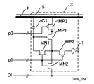
画素3は、表示領域5内においてマトリックス状(n行、m列)に配置されている。表示領域内の画素は、行方向(図1の横方向)に制御線によって共通に接続され、列方向(図1の縦方向)に信号線によって共通に接続されている。
The
行制御回路7には水平同期信号lkと走査開始信号vsが入力される。行制御回路7は、行毎に設けられた制御線p1(1)、p1(2)・・・p1(n)に制御信号を出力する。制御線p1は、同じ行に配置された画素3に共通に接続される。(以下、括弧とその中の行番号を省略した場合は任意行での制御線であることをあらわす。他の符号についても同じとする。)
画像信号発生回路となる列制御回路6にはサンプリング開始信号sp、クロック信号k、ビデオ信号videoが入力される。列制御回路6は、ビデオ信号videoを変換して信号線Dl(1)、Dl(2)・・・Dl(m)に画像信号を出力する。各信号線は同じ列に配置された画素3に共通に接続される。
The
A sampling control signal sp, a clock signal k, and a video signal video are input to the
本実施形態では、各列の信号線に信号切換手段であるトランジスタMN3(1)、MN3(2)・・・MN3(m)が配置される。トランジスタMN3(1)〜MN3(m)のドレインはそれぞれの列の信号線に接続され、ソースは固定信号源となる接地電位に接続されている。また、トランジスタMN3(1)〜MN3(m)のゲートには共通にモード切替線p2が接続されている。 In the present embodiment, transistors MN3 (1), MN3 (2)... MN3 (m), which are signal switching means, are arranged on the signal lines in each column. The drains of the transistors MN3 (1) to MN3 (m) are connected to the signal lines of the respective columns, and the sources are connected to a ground potential serving as a fixed signal source. Further, the mode switching line p2 is commonly connected to the gates of the transistors MN3 (1) to MN3 (m).
図2に画素3の一構成例を示す。
FIG. 2 shows a configuration example of the
画素3は、駆動トランジスタMP1と、スイッチとして動作するトランジスタMP2,MN1,MN2、容量C1、ならびにEL素子1で構成されている。これに、図1の制御線p1と信号線Dl、および不図示の電源から一定電圧(VDD)を供給する電源線2が接続されている。(図1では電源線2は省略されている。)EL素子の一端はグランド(接地)電位になっている。
The
電源線2は駆動トランジスタMP1のソースに接続され、ゲートは容量C1の一方の端子、スイッチMN1の一方の端子に接続される。容量C1の他方の端子は電源線2に接続される。スイッチMN1の他方の端子は駆動トランジスタMP1のドレインに接続され、またスイッチMP2の一方の端子に接続されている。スイッチMP2の他方の端子は有機EL素子1のアノード電極に接続されている。
The
駆動トランジスタMP1のドレインには、更にスイッチMN2の一方の端子が接続され、他方の端子は信号線Dlに接続されている。スイッチMN1,MN2,MP2のゲートは共通の制御線p1に接続されている。 One terminal of the switch MN2 is further connected to the drain of the driving transistor MP1, and the other terminal is connected to the signal line Dl. The gates of the switches MN1, MN2, and MP2 are connected to a common control line p1.
スイッチの極性は、ここでは、スイッチMN1,MN2はN型電界効果トランジスタ、スイッチMP2はP型電界効果トランジスタを使用している。しかし、製造プロセスもしくはTFTの特性に応じてN型をP型の極性のトランジスタ、P型をN型の極性のトランジスタに変更しても良い。 Here, the switches MN1 and MN2 use N-type field effect transistors, and the switch MP2 uses P-type field effect transistors. However, the N-type transistor may be changed to a P-type polarity transistor and the P-type transistor may be changed to an N-type polarity transistor according to the manufacturing process or TFT characteristics.
次に各画素3の動作について述べる。
(書き込み動作)
出力p1がHレベルになると、その行の画素は、図2のスイッチMN1、MN2がON状態、スイッチMP2がOFF状態、駆動トランジスタMP1はダイオード接続の状態になる。この状態で各々信号変換回路4で生成された電流信号は信号線Dlを通して駆動トランジスタMP1のゲート電圧を変化させ、信号変換回路4の電流に対応した電流値になり、ゲート電圧は容量C1に蓄えられる。
(表示動作)
出力p1がLレベルになると、図2のスイッチMN1、MN2がOFF状態、スイッチMP2がON状態になる。駆動トランジスタMP1は、書き込み時に容量C1蓄えられた電圧により定まる一定の電流を有機EL素子1に注入する。これによってEL素子が発光する。
Next, the operation of each
(Write operation)
When the output p1 becomes H level, the pixels in the row are in the ON state, the switch MP2 is in the OFF state, and the drive transistor MP1 is in the diode connection state in FIG. In this state, each current signal generated by the
(Display operation)
When the output p1 becomes L level, the switches MN1 and MN2 in FIG. 2 are turned off and the switch MP2 is turned on. The drive transistor MP1 injects a constant current determined by the voltage stored in the capacitor C1 at the time of writing into the
表示動作においては、EL素子に流れる電流が容量C1の電圧によって決定され、電源電圧やEL素子の電圧電流特性に依存しないようにする必要がある。このため、駆動トランジスタは飽和領域で動作させる。 In the display operation, the current flowing through the EL element is determined by the voltage of the capacitor C1, and it is necessary not to depend on the power supply voltage or the voltage-current characteristics of the EL element. For this reason, the driving transistor is operated in a saturation region.
Pチャネル型のMOSトランジスタでの飽和領域は、ゲート電位VG、ソース電位VS、ドレイン電位VDが
VS−VG>Vth、かつVD<VG
の関係を満たす動作範囲である。Vthはトランジスタが導通する閾値電圧である。
In the saturation region of a P-channel MOS transistor, the gate potential VG, source potential VS, and drain potential VD
VS−VG> Vth and VD <VG
This is an operating range that satisfies the above relationship. Vth is a threshold voltage at which the transistor becomes conductive.
飽和領域では、ドレイン電流がゲート−ソース間電圧だけで決まり、基本的にはドレイン−ソース間電圧によらない。これに対し、
VS−VG>Vth、かつVD>VG
となる線形領域では、ドレイン電流がドレイン−ソース間電圧に比例し、トランジスタがアナログスイッチとして働く。
In the saturation region, the drain current is determined solely by the gate-source voltage and basically does not depend on the drain-source voltage. In contrast,
VS−VG> Vth and VD> VG
In the linear region, the drain current is proportional to the drain-source voltage, and the transistor functions as an analog switch.
図3は列制御回路6の回路構成を示している。
FIG. 3 shows a circuit configuration of the
図3のDh1、Dh2、・・・、Dhmはレジスタ、MS1、MS2、・・・、MSmはスイッチトランジスタ、4(1)、4(2)、・・・、4(m)は信号変換回路、Dl(1)、Dl(2)、・・・、Dl(m)は信号線である。(各符号の括弧内の番号は列番号を表す。以下で()を省略した場合は任意の列でのそれを示す。)
Dh1、Dh2、・・・、DhmはそれぞれD型フリップフロップ回路であり、データ端子Dに入力された信号をクロック信号kの立ち上がりタイミングに同期してラッチするとともに出力端子Qに出力する。
In FIG. 3, Dh1, Dh2,..., Dhm are registers, MS1, MS2,..., MSm are switch transistors, 4 (1), 4 (2),. , Dl (1), Dl (2),..., Dl (m) are signal lines. (The number in parentheses for each symbol represents the column number. If () is omitted below, it indicates that in any column.)
Dh1, Dh2,..., Dhm are each a D-type flip-flop circuit that latches the signal input to the data terminal D in synchronization with the rising timing of the clock signal k and outputs it to the output terminal Q.
Dh1、Dh2、・・・、Dhmは、それぞれ前段の出力をデータ端子Dに入力し、出力端子Qを次段の入力としているので、初段Dh1の入力信号Dを、クロック信号kの1周期ずつ遅れて次々と転送するシフトレジスタを構成している。 Dh1, Dh2,..., Dhm each input the output of the previous stage to the data terminal D and the output terminal Q as the input of the next stage, so that the input signal D of the first stage Dh1 is changed by one cycle of the clock signal k. A shift register for transferring data one after another with a delay is configured.
トランジスタMS1〜MSmの一方の端子には共通してビデオ信号videoが入力され、他方の端子はそれぞれ信号変換回路4(1)、4(2)・・・4(m)に接続される。信号変換回路4の出力は信号線となる信号線Dl(1)、Dl(2)・・・Dl(m)となる。
The video signal video is commonly input to one terminal of the transistors MS1 to MSm, and the other terminal is connected to the signal conversion circuits 4 (1), 4 (2)... 4 (m), respectively. The output of the
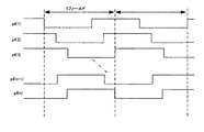
列制御回路6の動作について図5のタイミングチャートを用いて説明する。
The operation of the
初段のレジスタDh1のデータ端子Dに入力されるサンプリング開始信号spは、クロック信号kの1周期の間だけH(High)レベルになる。レジスタDh1は、クロック信号kの立ち上がりタイミングに同期してサンプリング開始信号spをラッチするとともに、出力端子Qからサンプリング信号p5(1)として出力する。 The sampling start signal sp input to the data terminal D of the first-stage register Dh1 becomes H (High) level only for one period of the clock signal k. The register Dh1 latches the sampling start signal sp in synchronization with the rising timing of the clock signal k and outputs it from the output terminal Q as the sampling signal p5 (1).
クロック信号kの次の立ち上がりに同期して、出力p5(1)はL(Low)レベルに戻り、同時に次のレジスタDh2の出力p5(2)がHレベルに変化する。このようにして、区間th(1)の間Hレベルになるサンプリング信号sp(1)が生成される。 In synchronization with the next rise of the clock signal k, the output p5 (1) returns to the L (Low) level, and at the same time, the output p5 (2) of the next register Dh2 changes to the H level. In this way, the sampling signal sp (1) that is at the H level during the section th (1) is generated.
レジスタDh1の出力端子Qは次段のレジスタDh2のデータ端子Dに接続されているので、以下次々と信号がシフトされ、区間th(m)までシフト動作を続ける。この結果、p5(1)から1クロック周期ずつ遅れたサンプリング信号p5(2)、・・・、p5(m)が生成される。 Since the output terminal Q of the register Dh1 is connected to the data terminal D of the register Dh2 at the next stage, the signals are shifted one after another, and the shift operation is continued until the section th (m). As a result, sampling signals p5 (2),..., P5 (m) that are delayed by one clock cycle from p5 (1) are generated.
ビデオ信号videoは、外部から画像情報がシリアルに伝送されてくる信号であり、画像情報に応じて電圧または電流の振幅を変化させる。 The video signal video is a signal in which image information is serially transmitted from the outside, and changes the amplitude of the voltage or current in accordance with the image information.
サンプリング信号p5がHレベルの状態の時に、スイッチトランジスタMSがON状態になり、ビデオ信号videoをサンプリングしてその列の信号変換回路4に入力する。
When the sampling signal p5 is in the H level, the switch transistor MS is turned on, and the video signal video is sampled and input to the
図4は1つの信号変換回路4の回路図である。
FIG. 4 is a circuit diagram of one
ビデオ信号videoはトランジスタMN6のドレインに入力される。トランジスタMN6はドレイン−ゲートが短絡され、容量C2が接続されている。トランジスタMN6のソース、容量C2の一端は接地電位(グランド)に接続されている。トランジスタMN6のゲートはトランジスタMN5のゲートに接続されている。トランジスタMN5のソースはグランドに接続され、ドレインは信号変換回路4の出力となり、信号線Dlに接続される。
The video signal video is input to the drain of the transistor MN6. The transistor MN6 has a drain-gate short-circuited and a capacitor C2. The source of the transistor MN6 and one end of the capacitor C2 are connected to the ground potential (ground). The gate of the transistor MN6 is connected to the gate of the transistor MN5. The source of the transistor MN5 is connected to the ground, and the drain is the output of the
サンプリングされ信号変換回路4に入力されたvideo信号は、それが電圧信号である場合は容量C2にそのまま蓄えられ、電流信号である場合はダイオード接続されているトランジスタMN6のゲート電圧が容量C2に蓄えられる。そして信号線Dlに出力される際には、トランジスタMN6とトランジスタMN5のLWサイズ比に応じて変換増幅された電流信号を出力する。なお、LWサイズ比は入力側においては表示装置に入力するドライバ回路(IC)との配線インピーダンス、ピン容量、そして出力側において表示素子である有機EL素子1の特性において決定される。また、信号線に電流信号が出力されるとして場合について説明したが、前述した配線インピーダンスやピン容量の関係により電流書き込みが困難な場合は、トランジスタMN5の代わりにソースフォロワ回路を用いて、C2に蓄えられた電圧をそのまま信号線に出力しても良い。
The video signal sampled and input to the
図6は行制御回路7の構成を示すブロック図、図7はその動作を示すタイミングチャートである。
FIG. 6 is a block diagram showing the configuration of the
行制御回路7は、レジスタ列Dv1−Dvnからなるシフトレジスタで構成される。
The
走査開始信号vsは水平同期クロック信号lkの1周期分の信号として初段レジスタDv1に入力される。レジスタDv1は、水平同期クロック信号lkの立ち上がりタイミングでデータ端子Dの信号をラッチするとともにそれを出力端子Qに出力する。出力は次段のレジスタDv2のデータ端子Dに接続されている。 The scanning start signal vs is input to the first stage register Dv1 as a signal for one cycle of the horizontal synchronization clock signal lk. The register Dv1 latches the signal at the data terminal D at the rising timing of the horizontal synchronization clock signal lk and outputs it to the output terminal Q. The output is connected to the data terminal D of the register Dv2 at the next stage.
次のクロックの立ち上がりタイミングではvsはLレベルなので出力p1(1)はLレベルに戻り次のレジスタDv2の出力p1(2)はHレベルに変化する。以下、区間tv(m)までシフト動作を続けるべくクロックは入力される。 Since vs is at the L level at the rising timing of the next clock, the output p1 (1) returns to the L level and the output p1 (2) of the next register Dv2 changes to the H level. Hereinafter, the clock is input to continue the shift operation until the interval tv (m).
図3において、列制御回路6は、画像信号videoのサンプリングと、ある行の画素の書き込みを同時に行うことになる。サンプリング後の画素3への書き込み時間に余裕が無い場合は、信号変換回路4を2行分用意し、1行分の信号変換回路4には画像信号videoのサンプリングを行う。そしてもう1行分の信号変換回路4にはサンプリングを行った後のvideo変換情報を保持した状態で画素の書き込みを行う。この2行の役割を行ごとに入れ替えるトグル信号を新たに設けて交互に行えば画素3への書き込み時間は1行分のサンプリング時間確保される。
In FIG. 3, the
次に図1のトランジスタMN3(1)〜MN3(m)の役割と動作について説明する。
(通常表示)
通常の画像表示を行う時は、図1のモード切替線p2をLレベルの状態にしておく。トランジスタMN3(1)〜MN3(m)はオフの状態になり、信号線は接地電位から切り離されている。
Next, the role and operation of the transistors MN3 (1) to MN3 (m) in FIG. 1 will be described.
(Normal display)
When normal image display is performed, the mode switching line p2 in FIG. 1 is set to the L level. The transistors MN3 (1) to MN3 (m) are turned off, and the signal line is disconnected from the ground potential.
行制御回路7の出力する制御信号p1(1)〜p1(n)によって、各行の画素3が選択される。選択された行の画素は、信号線から画像信号を受け取り、上で説明した書き込み動作を行う。非選択行の画素は表示動作を行う。すなわち、容量C2に保持された電圧に応じてEL素子に電流を出力する。この電流は、容量C2に保持された電圧と駆動トランジスタMP1の特性とによって決まる電流であり、基本的に電源電圧やEL素子の特性には依存しない。これを電流駆動方式と呼ぶことにする。
The
表示状態において、駆動トランジスタMP1のソース―ドレイン間電圧はELに流す電流によって変化する。駆動トランジスタMP1のゲート電位(すなわち書き込み時の信号線電位)が電源電圧VDDから低い方向に離れるにつれて、EL電流が増えEL素子の両端電圧が大きくなる。駆動トランジスタMP1は飽和領域(VG>VD)で動作させなければならないから、信号線電位は、最大電流時、すなわちEL素子の端子間電圧が最大になった時のドレイン電位より高い範囲になければならない。 In the display state, the source-drain voltage of the driving transistor MP1 varies depending on the current flowing through the EL. As the gate potential of the driving transistor MP1 (that is, the signal line potential at the time of writing) moves away from the power supply voltage VDD in the lower direction, the EL current increases and the voltage across the EL element increases. Since the driving transistor MP1 must be operated in the saturation region (VG> VD), the signal line potential must be higher than the drain potential at the maximum current, that is, when the voltage between the terminals of the EL element is maximized. Don't be.
電源電圧VDDと有機EL素子1の最大オン電圧Vonとの差(VDD−Von)が十分大きく確保されていれば、通常の画像信号の変調範囲では飽和(5極管)領域で動作することが保証される。
(エージング)
エージング処理は、EL素子または薄膜トランジスタに、一定時間、一定電流を流して特性を安定化させる処理である。製造工程に組み込まれることが多いので、短時間で処理を終えるために、通常の表示動作よりも大きな電流で駆動する。
If a sufficiently large difference (VDD−Von) between the power supply voltage VDD and the maximum ON voltage Von of the
(aging)
The aging process is a process of stabilizing the characteristics by flowing a constant current through the EL element or the thin film transistor for a certain period of time. Since it is often incorporated into the manufacturing process, in order to finish the processing in a short time, the display is driven with a larger current than in a normal display operation.
エージング処理を行うには、図1のモード切替線p2をHレベルにする。 To perform the aging process, the mode switching line p2 in FIG. 1 is set to the H level.
p2がHレベルなので、トランジスタMN3(1)〜MN3(m)がONになり、信号線が全てグランド(接地)電位になる。 Since p2 is at the H level, the transistors MN3 (1) to MN3 (m) are turned on, and the signal lines are all at the ground (ground) potential.
画素3は、制御信号p1がHレベルになった時に、グランド電位を書き込む。容量C1には電源電位と接地電位の差が保持される。
The
行制御回路7による行の制御は、通常表示のときと同様に、制御信号を印加することにより行を1行ずつ順次選択して書き込み動作を行い、その後の非選択時にELに電流を供給する。
As in the case of normal display, the
信号線に与えられる電位は必ずしも接地電位である必要はなく、一定の電圧信号または電流信号を供給する固定信号源であればよい。ただし、その固定信号は、画素に書き込まれた後、駆動トランジスタをアナログスイッチとして動作させるために、駆動トランジスタのゲート−ソース間電圧がドレイン−ソース電圧より大きくなるように設定される。 The potential applied to the signal line is not necessarily a ground potential, and may be a fixed signal source that supplies a constant voltage signal or current signal. However, the fixed signal is set so that the gate-source voltage of the drive transistor becomes larger than the drain-source voltage in order to operate the drive transistor as an analog switch after being written in the pixel.
制御信号p1がLレベルになると、駆動トランジスタMP1が導通する。このとき、EL素子には大きな電流が流れてドレイン電位が上昇するので、ゲート電位VGはドレイン電位VDより低くなる。このとき、駆動トランジスタは線形領域で動作し、アナログスイッチの働きをする。飽和トランジスタのオン抵抗は非常に小さいので、電源電圧は大部分がEL素子にかかり、EL素子に流れる電流は電源線の電圧で決まるようになる。 When the control signal p1 becomes L level, the drive transistor MP1 becomes conductive. At this time, since a large current flows through the EL element and the drain potential rises, the gate potential VG becomes lower than the drain potential VD. At this time, the driving transistor operates in a linear region and functions as an analog switch. Since the ON resistance of the saturation transistor is very small, most of the power supply voltage is applied to the EL element, and the current flowing through the EL element is determined by the voltage of the power supply line.
上で述べたように、この電流は通常の表示が行われるときの画像信号に応じた電流よりは大きく設定される。したがって、EL素子の端子間に生じる電圧も、通常表示の時の最大値よりさらに大きい電圧になる。画像信号が、駆動トランジスタを飽和領域で動作させる範囲に設定されている限り、この条件はつねに満足されている。 As described above, this current is set to be larger than the current corresponding to the image signal when normal display is performed. Therefore, the voltage generated between the terminals of the EL element is also higher than the maximum value during normal display. This condition is always satisfied as long as the image signal is set in a range in which the driving transistor operates in the saturation region.
EL素子の発光を電圧によって制御する方式は電圧駆動方式と呼ばれる。以下、電圧駆動方式でELを駆動させることを第1の駆動モード(あるいは第1のモード)という。 A method of controlling light emission of the EL element by voltage is called a voltage driving method. Hereinafter, driving the EL by the voltage driving method is referred to as a first driving mode (or a first mode).
これに対し、先に説明した通常の表示においては、駆動トランジスタを飽和動作させ、EL素子に流れる電流が制御される。すなわちEL素子は電流駆動方式で駆動される。これを第2の駆動モード(あるいは第2のモード)ということにする。 On the other hand, in the normal display described above, the drive transistor is operated in saturation, and the current flowing through the EL element is controlled. That is, the EL element is driven by a current driving method. This is called the second drive mode (or second mode).
このように、エージング状態では駆動トランジスタMP1は線形領域(3極管領域)で動作する。エージングに必要な電流は電源電圧VDDを変化させて調節することができる。 Thus, in the aging state, the driving transistor MP1 operates in the linear region (triode region). The current required for aging can be adjusted by changing the power supply voltage VDD.
本実施形態では、スイッチトランジスタMN3(1)〜MN3(m)は電流駆動と電圧駆動の2つのモードを切り換えるスイッチ素子として働く。 In the present embodiment, the switch transistors MN3 (1) to MN3 (m) function as switching elements that switch between two modes of current driving and voltage driving.
スイッチトランジスタMN3の代わりに、信号変換回路4の内部にモード切り替え手段を設けてもよい。
Instead of the switch transistor MN3, mode switching means may be provided inside the
具体的には、図4の回路とは別にエージング用の電圧信号を生成する回路を設け、この回路の出力と図4の回路の出力とをスイッチで切り替えて信号線に供給する。あるいは、信号変換回路4のトランジスタMN5にて画像信号電流より大きなエージング用信号電流を発生させてもよい。
エージングは、基板に、EL素子と画素を含む画素、制御線、ならびに信号線を形成し、これらを駆動する電源や信号を発生する回路を接続した後に、第1の駆動モードに設定して、画素に信号線から固定信号を書き込み、EL素子を電圧駆動することによって行われる。エージングは、製造工程の最終工程でEL素子の初期の特性変化を通過させるために行われるが、表示装置として用いられているときに、通常表示状態の前に特性安定化のために行われてもよい。
Specifically, a circuit for generating an aging voltage signal is provided separately from the circuit of FIG. 4, and the output of this circuit and the output of the circuit of FIG. 4 are switched by a switch and supplied to the signal line. Alternatively, an aging signal current larger than the image signal current may be generated by the transistor MN5 of the
Aging is performed by forming a pixel including EL elements and pixels, a control line, and a signal line on a substrate, connecting a power source for driving these and a circuit for generating a signal, and then setting the first driving mode. This is done by writing a fixed signal from the signal line to the pixel and driving the EL element with voltage. Aging is performed in order to pass the initial characteristic change of the EL element in the final step of the manufacturing process, but when used as a display device, it is normally performed for characteristic stabilization before the display state. Also good.
(第2の実施の形態)
本発明の第2の実施形態においては、画素3に接続される電源線を2つ以上とし、通常表示状態とエージング状態とで取り替えて使用する。その他は第1の実施形態と同じである。
(Second Embodiment)
In the second embodiment of the present invention, two or more power lines are connected to the
図8は、電源線を2本とした例である。2本の電源線は、太さが異なり、したがって画素から見たインピーダンスが異なる。素子や制御線の記号が図2と同じものは同じ作用をするものとする。 FIG. 8 shows an example in which two power supply lines are used. The two power supply lines have different thicknesses, and thus have different impedances as viewed from the pixels. Elements having the same element and control line symbols as those in FIG.
2本の電源線のうち、電源線2は電源線5よりも太いものとする。電源線2を電源線5よりも太くすることは、電源線2の幅を電源線5よりも広くする、電源線2の層厚を電源線5の層厚よりも厚くする等で実現できる。これらの2本の電源線2、5は表示領域5内で結線されることはなく、表示領域の外から別々に供給される。
Of the two power lines, the
電源線2と駆動トランジスタMP1の一方の主電極となるソースとの間には新たなスイッチMP3が設けられ、ゲートには第2の制御線p3が設けられている。駆動トランジスタMP1のソースはスイッチMP3を介して電源線2と電気的に接続されることになる。第2の制御線p3は画素3(1,1)〜(n,m)について共通に接続される。
A new switch MP3 is provided between the
表示状態においては、第2の制御線p3をLレベルの状態にしておく。電力供給は電源線2と電源線5の両方から供給されるが、よりインピーダンスの低い電源線2から主に供給される。
In the display state, the second control line p3 is kept at the L level. The power is supplied from both the
エージング状態においては第2の制御線p3をHレベルの状態にする。これにより電源供給は電源線5のみの供給状態になる。電源の配線インピーダンスが高いので、表示領域5の中でEL素子に印加される電圧にばらつきを生じ、表示領域の周辺で明るく、中央で暗いシェーディング現象を誘発することになるが、この条件でエージング(第1の駆動モード)を行うことにする。
In the aging state, the second control line p3 is set to the H level. As a result, the power is supplied only to the
エージング中、高輝度で発光した周辺部のEL素子は、中央部のEL素子に比べて特性変化が速く進むので、徐々に輝度が低下し、エージング終了時には周辺部と中央部の輝度差はエージング前よりも小さくなっている。 During aging, the peripheral EL element that emits light with high brightness undergoes a faster characteristic change than the central EL element, so that the luminance gradually decreases, and at the end of aging, the luminance difference between the peripheral part and the central part is aging. It is smaller than before.
この状態で、電源線2を接続し、駆動モードを通常表示状態(第2の駆動モード)に切り換えると、同じ電流に対して中央部の画素は周辺部の画素よりも輝度が高いので、インピーダンス差の小さい電源線からの電流供給により、周辺部との輝度差がほとんどない状態になる。
In this state, when the
電源2と5のインピーダンス差の程度によっては、中央部の輝度が周辺部より高くなることもある。ユーザの意向に応じて適宜エージング条件を変えることにより、中央部と周辺部の輝度差を調整することもできる。
Depending on the degree of impedance difference between the
(第3の実施の形態)
本発明の第3の実施形態は、行制御回路から供給される制御線p1とは独立に、有機EL素子1に流れる電流のオン/オフを切り替える新たな第3の制御線p4を設けるものである。
(Third embodiment)
In the third embodiment of the present invention, a new third control line p4 for switching on / off of the current flowing through the
図9に制御線を2本設けた場合を示す。第1の実施形態では制御線p1にてオンオフが制御されていたスイッチMP2を、新たに設けた第3の制御線p4によって制御する。図9の回路で素子や制御線の記号が図2と同じものは同じ作用をするものとし詳細な説明を省略する。 FIG. 9 shows a case where two control lines are provided. In the first embodiment, the switch MP2 whose on / off is controlled by the control line p1 is controlled by the newly provided third control line p4. In the circuit of FIG. 9, the same elements and control line symbols as those in FIG.
表示状態、またはエージング状態において、第3の制御線p4は1フィールドの一部の期間だけLレベルになり、EL素子に電流を流す。図10は第3の制御線p4に与える制御信号の1例である。行の制御信号に同期して第3の制御線p4(1)〜p4(n)に1Hずつずれた制御信号を加え、順次点灯―消灯を行ってもよい。またはエージング状態においては独立に画素3の第3の制御線p4を全て一括にして行制御回路と非同期にパルス駆動しても良い。
In the display state or the aging state, the third control line p4 is at the L level only during a part of one field, and a current flows through the EL element. FIG. 10 is an example of a control signal applied to the third control line p4. A control signal shifted by 1H may be applied to the third control lines p4 (1) to p4 (n) in synchronization with the row control signal to sequentially turn on and off. Alternatively, in the aging state, all the third control lines p4 of the
エージング状態においては、電圧駆動により有機EL素子1に大きな電流が流れると、素子が発熱する。
そこで第3の制御線p4をパルス駆動することで発光期間を少なくし、有機EL素子1への電力供給を適宜遮断する。輝度計を用いてパルス駆動の周期やデューティを変えることにより精度の高いエージング処理が可能になり製造時の工程管理も容易になる。
In the aging state, when a large current flows through the
Therefore, the third control line p4 is pulse-driven to reduce the light emission period and appropriately cut off the power supply to the
本実施形態では、エージング処理時に有機EL素子をパルス駆動することにより間欠点灯させる。輝度を計測し、点灯の周期やデューティを可変しながら輝度を適宜設定できるので、有機EL素子を破壊することなく正確なエージング処理を行うことができる。 In the present embodiment, intermittent lighting is performed by driving the organic EL element in pulses during the aging process. Since the luminance can be measured and the luminance can be appropriately set while varying the lighting cycle and duty, an accurate aging process can be performed without destroying the organic EL element.
点灯デューティのみならず、電源線の電圧を変えて輝度を調整してもよい。 In addition to the lighting duty, the luminance may be adjusted by changing the voltage of the power supply line.
(第4の実施の形態)
本実施形態は、図9に示した画素における第3の制御線p4を、例えばR、G、Bの各色画素ごとに分けて独立に駆動したものである。
例えば電源電圧や第3の制御線p4に印加するパルスの幅が同一条件において、エージングにかかる時間をR>G>Bとする。この場合、図11に示すように一周期におけるスイッチMP2のON状態(Lレベル区間)がR>G>Bとなるようにする。すなわち、{R画素の第3の制御線p4(R)のLレベル区間長}>{G画素の第3の制御線p4(G)のLレベル区間長}>{B画素の第3の制御線p4(B)のLレベル区間長}となるように設定している。これにより、同一時間経過後における実効エージング時間をR>G>Bとすることが可能になる。従って単純な工程にてエージング処理を精度良く行うことが出来る。
(Fourth embodiment)
In the present embodiment, the third control line p4 in the pixel shown in FIG. 9 is driven separately for each color pixel of R, G, B, for example.
For example, assuming that the power supply voltage and the pulse width applied to the third control line p4 are the same, the time required for aging is R>G> B. In this case, as shown in FIG. 11, the ON state (L level section) of the switch MP2 in one cycle is set to satisfy R>G> B. That is, {L level section length of third control line p4 (R) of R pixel}> {L level section length of third control line p4 (G) of G pixel}> {Third control of B pixel L level section length of line p4 (B)} is set. Thereby, the effective aging time after the lapse of the same time can be set to R>G> B. Therefore, the aging process can be performed with high accuracy by a simple process.
各色ごとに独立した電源線が割り当てられる構成ならば、前述したパルス幅を各色一定もしくは常にON状態にしたまま独立に電圧を制御しても良い。すなわち各色の電流効率や初期劣化の時間を勘案し、R、G、B異なる電圧値に設定することによりエージング処理を同一時間内に精度良く行うことも可能である。 As long as an independent power supply line is assigned to each color, the voltage may be controlled independently with the above-described pulse width constant for each color or always ON. In other words, the aging process can be accurately performed within the same time by setting the voltage values different from R, G, and B in consideration of the current efficiency of each color and the time of initial deterioration.
また色度計を用いることにより、モニタリングした情報を前述の制御線p4(R),P4(G),P4(B)に印加するパルス幅や電圧値を適宜変えたりすることで、更に精度を高めたエージング処理を行うことができる。
以上説明したとおり、本発明は、表示状態とエージング状態において異なる駆動方式を実施する。表示状態では電流駆動方式を採用する。駆動トランジスタで制御された電流を有機EL素子に注入することにより、電源インピーダンスによらない品質の高い駆動が得られる。また、エージング状態では電圧駆動方式を実施することにより短期間のエージングを可能にする。
Further, by using a chromaticity meter, the accuracy can be further improved by appropriately changing the pulse width and voltage value of the monitored information applied to the control lines p4 (R), P4 (G), and P4 (B). An enhanced aging process can be performed.
As described above, the present invention implements different driving methods in the display state and the aging state. In the display state, the current drive method is adopted. By injecting the current controlled by the driving transistor into the organic EL element, high quality driving independent of the power source impedance can be obtained. Further, in the aging state, the aging for a short time is enabled by implementing the voltage driving method.
1 有機EL素子
2 電源線
3 画素
4 信号変換回路
5 第2の電源線
6 列制御回路
7 行制御回路
MN1、MN2、MN5、MN6、MS1〜MSm、MN3(1)〜MN3(m) n型トランジスタ
MP1、MP2 p型トランジスタ
Dh1〜Dhm、Dv1〜Dvn レジスタ
DESCRIPTION OF
MP1, MP2 p-type transistors Dh1-Dhm, Dv1-Dvn registers
Claims (14)
前記発光素子に前記駆動トランジスタを介して前記電源線の電圧を印加する第1のモードと、前記駆動トランジスタのゲート電圧に基づいて、前記電源線から前記発光素子に電流を供給して前記発光素子を発光させる第2のモードとを有し、
前記第1のモードで前記駆動トランジスタを動作させるために前記画素に書き込む固定信号と、前記第2のモードで前記駆動トランジスタを動作させるために前記画素に書き込む画像信号とを切り換えて前記信号線に与える切換手段を備えたことを特徴とするアクティブマトリックス型表示装置。 Pixels having light emitting elements, and power source lines and driving transistors each connected to the light emitting elements are arranged in a matrix, and a control line commonly connected to the pixels arranged in a row direction; An active matrix type having a signal line commonly connected to the pixels arranged in a column direction, selecting the pixel for each row by the control line, and writing a signal from the signal line to the selected pixel A display device,
Based on a first mode in which a voltage of the power supply line is applied to the light emitting element via the driving transistor and a gate voltage of the driving transistor, a current is supplied from the power supply line to the light emitting element, and the light emitting element is supplied. And a second mode for emitting light,
A fixed signal written to the pixel to operate the driving transistor in the first mode and an image signal written to the pixel to operate the driving transistor in the second mode are switched to the signal line. An active matrix display device comprising switching means for giving.
前記画素、前記制御線、前記信号線、ならびに前記制御線と前記信号線に信号を印加する手段を形成する工程と、
前記制御線に前記制御信号を印加して行ごとに前記画素を選択して、選択した前記画素に前記信号線から固定信号を書き込み、前記発光素子に前記駆動トランジスタを介して前記電源線の電圧を印加する工程と
を有することを特徴とするアクティブマトリックス型表示装置の製造方法。 Pixels having light emitting elements, and power source lines and driving transistors each connected to the light emitting elements are arranged in a matrix, and a control line commonly connected to the pixels arranged in a row direction; A signal line connected in common to the pixels arranged in a column direction, applying a control signal to the control line to select the pixel for each row, and selecting an image from the signal line on the selected pixel A method of manufacturing an active matrix display device that displays an image by writing a signal and supplying a current corresponding to the image signal from the power line to the light emitting element to cause the light emitting element to emit light,
Forming the pixel, the control line, the signal line, and means for applying a signal to the control line and the signal line;
The control signal is applied to the control line to select the pixel for each row, a fixed signal is written to the selected pixel from the signal line, and the voltage of the power supply line is applied to the light emitting element via the driving transistor. And a method of manufacturing an active matrix display device.
前記制御線に前記制御信号を印加して行ごとに前記画素を選択し、選択した前記画素に前記信号線から固定信号を書き込むことにより、前記発光素子に、前記駆動トランジスタを介して前記電源線の電圧を印加する第1の駆動モードと、
前記制御線に前記制御信号を印加して行ごとに前記画素を選択し、選択した前記画素に前記信号線から画像信号を書き込むことにより、前記電源線から前記画像信号に基づく電流を前記発光素子に供給して前記発光素子を発光させる第2の駆動モードと、
を切り替えることを特徴とするアクティブマトリックス型表示装置の駆動方法。 Pixels having light emitting elements, and power source lines and driving transistors each connected to the light emitting elements are arranged in a matrix, and a control line commonly connected to the pixels arranged in a row direction; A driving method of an active matrix display device having a signal line commonly connected to the pixels arranged in a column direction,
The control signal is applied to the control line to select the pixel for each row, and a fixed signal is written from the signal line to the selected pixel, whereby the power supply line is connected to the light emitting element via the drive transistor. A first drive mode for applying a voltage of
Applying the control signal to the control line to select the pixel for each row, and writing an image signal from the signal line to the selected pixel, thereby supplying a current based on the image signal from the power line to the light emitting element And a second drive mode for causing the light emitting element to emit light,
A method of driving an active matrix display device, characterized by switching between the two.
Priority Applications (1)
| Application Number | Priority Date | Filing Date | Title |
|---|---|---|---|
| JP2008245939A JP2010078807A (en) | 2008-09-25 | 2008-09-25 | Active matrix type display device, method of manufacturing the same, and method of driving the same |
Applications Claiming Priority (1)
| Application Number | Priority Date | Filing Date | Title |
|---|---|---|---|
| JP2008245939A JP2010078807A (en) | 2008-09-25 | 2008-09-25 | Active matrix type display device, method of manufacturing the same, and method of driving the same |
Publications (1)
| Publication Number | Publication Date |
|---|---|
| JP2010078807A true JP2010078807A (en) | 2010-04-08 |
Family
ID=42209358
Family Applications (1)
| Application Number | Title | Priority Date | Filing Date |
|---|---|---|---|
| JP2008245939A Pending JP2010078807A (en) | 2008-09-25 | 2008-09-25 | Active matrix type display device, method of manufacturing the same, and method of driving the same |
Country Status (1)
| Country | Link |
|---|---|
| JP (1) | JP2010078807A (en) |
Cited By (3)
| Publication number | Priority date | Publication date | Assignee | Title |
|---|---|---|---|---|
| JP2013109868A (en) * | 2011-11-18 | 2013-06-06 | Panasonic Corp | Method of manufacturing display device, and display device |
| KR20200113787A (en) * | 2019-03-26 | 2020-10-07 | 주식회사 사피엔반도체 | Pixel using low-voltage transistor and Micro Display comprising the Pixel |
| CN114999398A (en) * | 2022-06-08 | 2022-09-02 | 京东方科技集团股份有限公司 | Pixel circuit, aging driving method thereof, array substrate and display device |
Citations (6)
| Publication number | Priority date | Publication date | Assignee | Title |
|---|---|---|---|---|
| JP2003280587A (en) * | 2002-01-18 | 2003-10-02 | Semiconductor Energy Lab Co Ltd | Display device, and display module and electronic apparatus using the same |
| JP2003330422A (en) * | 2002-05-17 | 2003-11-19 | Hitachi Ltd | Image display device |
| JP2005510768A (en) * | 2001-11-28 | 2005-04-21 | コーニンクレッカ フィリップス エレクトロニクス エヌ ヴィ | Electroluminescence display device |
| JP2006195030A (en) * | 2005-01-12 | 2006-07-27 | Sony Corp | Self-luminous device aging method, manufacturing method, and aging device |
| JP2006337992A (en) * | 2005-05-02 | 2006-12-14 | Semiconductor Energy Lab Co Ltd | Driving method of display device |
| JP2008064806A (en) * | 2006-09-04 | 2008-03-21 | Sanyo Electric Co Ltd | Defect inspection method and defect inspection apparatus for electroluminescence display device, and method for manufacturing electroluminescence display device using them |
-
2008
- 2008-09-25 JP JP2008245939A patent/JP2010078807A/en active Pending
Patent Citations (6)
| Publication number | Priority date | Publication date | Assignee | Title |
|---|---|---|---|---|
| JP2005510768A (en) * | 2001-11-28 | 2005-04-21 | コーニンクレッカ フィリップス エレクトロニクス エヌ ヴィ | Electroluminescence display device |
| JP2003280587A (en) * | 2002-01-18 | 2003-10-02 | Semiconductor Energy Lab Co Ltd | Display device, and display module and electronic apparatus using the same |
| JP2003330422A (en) * | 2002-05-17 | 2003-11-19 | Hitachi Ltd | Image display device |
| JP2006195030A (en) * | 2005-01-12 | 2006-07-27 | Sony Corp | Self-luminous device aging method, manufacturing method, and aging device |
| JP2006337992A (en) * | 2005-05-02 | 2006-12-14 | Semiconductor Energy Lab Co Ltd | Driving method of display device |
| JP2008064806A (en) * | 2006-09-04 | 2008-03-21 | Sanyo Electric Co Ltd | Defect inspection method and defect inspection apparatus for electroluminescence display device, and method for manufacturing electroluminescence display device using them |
Cited By (5)
| Publication number | Priority date | Publication date | Assignee | Title |
|---|---|---|---|---|
| JP2013109868A (en) * | 2011-11-18 | 2013-06-06 | Panasonic Corp | Method of manufacturing display device, and display device |
| KR20200113787A (en) * | 2019-03-26 | 2020-10-07 | 주식회사 사피엔반도체 | Pixel using low-voltage transistor and Micro Display comprising the Pixel |
| KR102228084B1 (en) * | 2019-03-26 | 2021-03-16 | 주식회사 사피엔반도체 | Pixel using low-voltage transistor and Micro Display comprising the Pixel |
| CN114999398A (en) * | 2022-06-08 | 2022-09-02 | 京东方科技集团股份有限公司 | Pixel circuit, aging driving method thereof, array substrate and display device |
| CN114999398B (en) * | 2022-06-08 | 2023-10-24 | 京东方科技集团股份有限公司 | Pixel circuit and aging driving method thereof, array substrate, display device |
Similar Documents
| Publication | Publication Date | Title |
|---|---|---|
| CN106558287B (en) | Organic light-emitting pixel driving circuit, driving method and organic light-emitting display panel | |
| US11244598B2 (en) | Pixel circuit, driving method, and display apparatus | |
| JP7672820B2 (en) | Driving circuit, driving method thereof, and display device | |
| KR102582551B1 (en) | Pixel driving circuit and driving method thereof, and display panel | |
| US10269297B2 (en) | Pixel circuit and driving method thereof, and display panel | |
| CN107274825B (en) | Display panel, display device, pixel driving circuit and control method thereof | |
| CN105931599B (en) | Pixel-driving circuit and its driving method, display panel, display device | |
| CN113053301B (en) | Pixel driving circuit, pixel driving method, display panel and display device | |
| CN111105751B (en) | Display device, method for driving display device, and electronic device | |
| US9349313B2 (en) | Display device and driving method thereof | |
| CN110782831A (en) | Pixel drive circuit, display device, and pixel drive circuit driving method | |
| CN102549646B (en) | Display device and method of driving same | |
| CN109979384B (en) | Pixel driving circuit, pixel circuit, display device, and pixel driving method | |
| CN104252845A (en) | Pixel driving circuit, pixel driving method, display panel and display device | |
| KR20110139764A (en) | Display Devices Using Capacitor-Coupled Light Emitting Control Transistors | |
| US11615738B2 (en) | Pixel driving circuit and driving method therefor, display panel, and display apparatus | |
| CN113168806B (en) | Pixel driving circuit, pixel driving method, display panel and display device | |
| CN112837649B (en) | Pixel driving circuit, driving method thereof, display panel and display device | |
| CN112820236B (en) | Pixel driving circuit and driving method thereof, display panel, and display device | |
| CN113077751A (en) | Pixel driving circuit, driving method thereof and display panel | |
| KR100639690B1 (en) | Image display apparatus without 0ccurrence of nonuniform display | |
| JP2011002845A (en) | Driving method for electrooptical device | |
| CN112992075A (en) | Pixel driving circuit, pixel driving method, pixel structure and display device | |
| WO2021047562A1 (en) | Pixel driving circuit, pixel unit, driving method, array substrate, and display device | |
| KR20090116402A (en) | Display device |
Legal Events
| Date | Code | Title | Description |
|---|---|---|---|
| RD04 | Notification of resignation of power of attorney |
Free format text: JAPANESE INTERMEDIATE CODE: A7424 Effective date: 20100201 |
|
| RD01 | Notification of change of attorney |
Free format text: JAPANESE INTERMEDIATE CODE: A7421 Effective date: 20100630 |
|
| A621 | Written request for application examination |
Free format text: JAPANESE INTERMEDIATE CODE: A621 Effective date: 20110926 |
|
| A977 | Report on retrieval |
Free format text: JAPANESE INTERMEDIATE CODE: A971007 Effective date: 20121022 |
|
| A131 | Notification of reasons for refusal |
Free format text: JAPANESE INTERMEDIATE CODE: A131 Effective date: 20121113 |
|
| A521 | Request for written amendment filed |
Free format text: JAPANESE INTERMEDIATE CODE: A523 Effective date: 20130115 |
|
| A02 | Decision of refusal |
Free format text: JAPANESE INTERMEDIATE CODE: A02 Effective date: 20131105 |