JP4846999B2 - Image display device - Google Patents
Image display device Download PDFInfo
- Publication number
- JP4846999B2 JP4846999B2 JP2004305241A JP2004305241A JP4846999B2 JP 4846999 B2 JP4846999 B2 JP 4846999B2 JP 2004305241 A JP2004305241 A JP 2004305241A JP 2004305241 A JP2004305241 A JP 2004305241A JP 4846999 B2 JP4846999 B2 JP 4846999B2
- Authority
- JP
- Japan
- Prior art keywords
- pixel
- video signal
- image display
- signal voltage
- pixels
- Prior art date
- Legal status (The legal status is an assumption and is not a legal conclusion. Google has not performed a legal analysis and makes no representation as to the accuracy of the status listed.)
- Expired - Lifetime
Links
- 239000003990 capacitor Substances 0.000 claims description 17
- 239000000758 substrate Substances 0.000 claims description 9
- 238000000295 emission spectrum Methods 0.000 claims description 3
- 238000005401 electroluminescence Methods 0.000 description 50
- 238000010586 diagram Methods 0.000 description 21
- 239000011521 glass Substances 0.000 description 7
- 239000011159 matrix material Substances 0.000 description 4
- 238000005516 engineering process Methods 0.000 description 2
- 238000000034 method Methods 0.000 description 2
- 229910021420 polycrystalline silicon Inorganic materials 0.000 description 2
- 238000003908 quality control method Methods 0.000 description 2
- 238000009825 accumulation Methods 0.000 description 1
- 230000008859 change Effects 0.000 description 1
- 238000007796 conventional method Methods 0.000 description 1
- 230000007423 decrease Effects 0.000 description 1
- 230000006870 function Effects 0.000 description 1
- 230000006872 improvement Effects 0.000 description 1
- 239000000203 mixture Substances 0.000 description 1
- 230000003287 optical effect Effects 0.000 description 1
- 230000009467 reduction Effects 0.000 description 1
- 230000004044 response Effects 0.000 description 1
- 239000004065 semiconductor Substances 0.000 description 1
- 239000010409 thin film Substances 0.000 description 1
Images


Classifications
-
- G—PHYSICS
- G09—EDUCATION; CRYPTOGRAPHY; DISPLAY; ADVERTISING; SEALS
- G09G—ARRANGEMENTS OR CIRCUITS FOR CONTROL OF INDICATING DEVICES USING STATIC MEANS TO PRESENT VARIABLE INFORMATION
- G09G3/00—Control arrangements or circuits, of interest only in connection with visual indicators other than cathode-ray tubes
- G09G3/20—Control arrangements or circuits, of interest only in connection with visual indicators other than cathode-ray tubes for presentation of an assembly of a number of characters, e.g. a page, by composing the assembly by combination of individual elements arranged in a matrix no fixed position being assigned to or needed to be assigned to the individual characters or partial characters
- G09G3/22—Control arrangements or circuits, of interest only in connection with visual indicators other than cathode-ray tubes for presentation of an assembly of a number of characters, e.g. a page, by composing the assembly by combination of individual elements arranged in a matrix no fixed position being assigned to or needed to be assigned to the individual characters or partial characters using controlled light sources
- G09G3/30—Control arrangements or circuits, of interest only in connection with visual indicators other than cathode-ray tubes for presentation of an assembly of a number of characters, e.g. a page, by composing the assembly by combination of individual elements arranged in a matrix no fixed position being assigned to or needed to be assigned to the individual characters or partial characters using controlled light sources using electroluminescent panels
- G09G3/32—Control arrangements or circuits, of interest only in connection with visual indicators other than cathode-ray tubes for presentation of an assembly of a number of characters, e.g. a page, by composing the assembly by combination of individual elements arranged in a matrix no fixed position being assigned to or needed to be assigned to the individual characters or partial characters using controlled light sources using electroluminescent panels semiconductive, e.g. using light-emitting diodes [LED]
- G09G3/3208—Control arrangements or circuits, of interest only in connection with visual indicators other than cathode-ray tubes for presentation of an assembly of a number of characters, e.g. a page, by composing the assembly by combination of individual elements arranged in a matrix no fixed position being assigned to or needed to be assigned to the individual characters or partial characters using controlled light sources using electroluminescent panels semiconductive, e.g. using light-emitting diodes [LED] organic, e.g. using organic light-emitting diodes [OLED]
- G09G3/3225—Control arrangements or circuits, of interest only in connection with visual indicators other than cathode-ray tubes for presentation of an assembly of a number of characters, e.g. a page, by composing the assembly by combination of individual elements arranged in a matrix no fixed position being assigned to or needed to be assigned to the individual characters or partial characters using controlled light sources using electroluminescent panels semiconductive, e.g. using light-emitting diodes [LED] organic, e.g. using organic light-emitting diodes [OLED] using an active matrix
- G09G3/3258—Control arrangements or circuits, of interest only in connection with visual indicators other than cathode-ray tubes for presentation of an assembly of a number of characters, e.g. a page, by composing the assembly by combination of individual elements arranged in a matrix no fixed position being assigned to or needed to be assigned to the individual characters or partial characters using controlled light sources using electroluminescent panels semiconductive, e.g. using light-emitting diodes [LED] organic, e.g. using organic light-emitting diodes [OLED] using an active matrix with pixel circuitry controlling the voltage across the light-emitting element
-
- G—PHYSICS
- G09—EDUCATION; CRYPTOGRAPHY; DISPLAY; ADVERTISING; SEALS
- G09G—ARRANGEMENTS OR CIRCUITS FOR CONTROL OF INDICATING DEVICES USING STATIC MEANS TO PRESENT VARIABLE INFORMATION
- G09G3/00—Control arrangements or circuits, of interest only in connection with visual indicators other than cathode-ray tubes
- G09G3/20—Control arrangements or circuits, of interest only in connection with visual indicators other than cathode-ray tubes for presentation of an assembly of a number of characters, e.g. a page, by composing the assembly by combination of individual elements arranged in a matrix no fixed position being assigned to or needed to be assigned to the individual characters or partial characters
- G09G3/2007—Display of intermediate tones
- G09G3/2014—Display of intermediate tones by modulation of the duration of a single pulse during which the logic level remains constant
-
- G—PHYSICS
- G09—EDUCATION; CRYPTOGRAPHY; DISPLAY; ADVERTISING; SEALS
- G09G—ARRANGEMENTS OR CIRCUITS FOR CONTROL OF INDICATING DEVICES USING STATIC MEANS TO PRESENT VARIABLE INFORMATION
- G09G2300/00—Aspects of the constitution of display devices
- G09G2300/08—Active matrix structure, i.e. with use of active elements, inclusive of non-linear two terminal elements, in the pixels together with light emitting or modulating elements
- G09G2300/0809—Several active elements per pixel in active matrix panels
- G09G2300/0819—Several active elements per pixel in active matrix panels used for counteracting undesired variations, e.g. feedback or autozeroing
-
- G—PHYSICS
- G09—EDUCATION; CRYPTOGRAPHY; DISPLAY; ADVERTISING; SEALS
- G09G—ARRANGEMENTS OR CIRCUITS FOR CONTROL OF INDICATING DEVICES USING STATIC MEANS TO PRESENT VARIABLE INFORMATION
- G09G2300/00—Aspects of the constitution of display devices
- G09G2300/08—Active matrix structure, i.e. with use of active elements, inclusive of non-linear two terminal elements, in the pixels together with light emitting or modulating elements
- G09G2300/0809—Several active elements per pixel in active matrix panels
- G09G2300/0842—Several active elements per pixel in active matrix panels forming a memory circuit, e.g. a dynamic memory with one capacitor
-
- G—PHYSICS
- G09—EDUCATION; CRYPTOGRAPHY; DISPLAY; ADVERTISING; SEALS
- G09G—ARRANGEMENTS OR CIRCUITS FOR CONTROL OF INDICATING DEVICES USING STATIC MEANS TO PRESENT VARIABLE INFORMATION
- G09G2320/00—Control of display operating conditions
- G09G2320/04—Maintaining the quality of display appearance
- G09G2320/043—Preventing or counteracting the effects of ageing
Landscapes
- Engineering & Computer Science (AREA)
- Physics & Mathematics (AREA)
- Computer Hardware Design (AREA)
- General Physics & Mathematics (AREA)
- Theoretical Computer Science (AREA)
- Control Of Indicators Other Than Cathode Ray Tubes (AREA)
- Control Of El Displays (AREA)
- Electroluminescent Light Sources (AREA)
Description
本発明は、高画質な表示が可能な画像表示装置に関する。 The present invention relates to an image display device capable of high-quality display.
以下に図12及び図13を用いて、従来の技術に関して説明する。
始めに従来例の構造について説明する。
The conventional technology will be described below with reference to FIGS.
First, the structure of the conventional example will be described.
図12は従来の技術を用いた有機EL(Electro Luminescence)ディスプレイの画素回路図である。各画素213には有機EL素子201が設けられており、有機EL素子201の一端は共通電極に接続され、他端はAZBスイッチ202、駆動TFT(Thin Film-Transistor)203を介して電源線212に接続されている。駆動TFT203のゲート−ドレイン間にはAZスイッチ204が、ゲート−ソース間には記憶容量205が接続されている。また駆動TFT203のゲートは、オフセットキャンセル容量206及び画素スイッチ207を介して信号線211に接続されている。なおAZBスイッチ202はAZB制御線208、AZスイッチ204はAZ制御線209、画素スイッチ207はゲート線210により制御される。
FIG. 12 is a pixel circuit diagram of an organic EL (Electro Luminescence) display using a conventional technique. Each
次に、従来例の動作について図13を用いて説明する。
図13は、従来例における画素への信号電圧書込み時の動作タイミング図である。ここで上記AZBスイッチ202、AZスイッチ204、画素スイッチ207は、図12に示したようにpMOSであるため、図13の各波形は下が各スイッチのオン(ON)、上がオフ(OFF)に対応している。
Next, the operation of the conventional example will be described with reference to FIG.
FIG. 13 is an operation timing chart at the time of writing a signal voltage to the pixel in the conventional example. Here, since the
書込みを選択された画素では、始めにゲート線210の信号SELによって画素スイッチ207がON、AZ制御線209によってAZスイッチ204がONになる。このときAZBスイッチ202はONであるため、有機EL素子201にはダイオード接続された駆動TFT203を介して電源線212から電流が流れる。
In the pixel selected for writing, first, the
次に、AZB制御線208の信号によってAZBスイッチ202がオフすると、駆動TFT203のドレイン端が閾値電圧Vthになった時点で、駆動TFT203はターンオフする。このとき信号線211には、「0レベル」の信号電圧データ(DAT)が印加されており、この電圧と上記閾値電圧Vthの差がオフセットキャンセル容量206に入力される。
Next, when the
次いで、AZ制御線209の信号によってAZスイッチ204がOFFした後に、信号線211には映像信号電圧が印加される。このとき駆動TFT203のゲートには、上記閾値電圧Vthに上記映像信号電圧に対応した電圧が生じ、この電圧はゲート線210の信号SELにより画素スイッチ207がOFFすることによって、記憶容量205に記憶される。この後、AZBスイッチ202がONすることで、画素213への信号電圧書込みが完了し、有機EL素子201は上記映像信号電圧に対応した輝度で次の書込み期間まで発光を続ける。
Next, the video signal voltage is applied to the
このような従来例は、例えば非特許文献1に記載されている。
Such a conventional example is described in
また他に、三角波を用いて有機EL素子を発光期間変調駆動する技術が、特許文献1や特許文献2に開示されている。
In addition,
前述した従来例においては、各画素に設けられた有機EL素子を、映像信号電圧に対応した輝度で発光させることができる。しかしながら、発明者らはディスプレイにおける発光特性は、このように映像信号電圧による一義的な発光のみで十分な高画質が得られるものではないことに気付いた。 In the above-described conventional example, the organic EL element provided in each pixel can emit light with a luminance corresponding to the video signal voltage. However, the inventors have realized that the light emission characteristics of the display do not provide sufficient image quality only by the unique light emission by the video signal voltage.
かつてTV用ディスプレイに表示される映像は、自然画が殆どであった。一方でパソコンや携帯電話のディスプレイに表示される映像は、テキストが殆どであった。しかしながら今後の情報化社会では、インターネットのホームページを見れば明らかなように、自然画とテキストが混在した映像が主体になる。このとき、ガンマ特性やピーク輝度に代表される信号−輝度特性は、自然画とテキストの両者で最適化することが望ましいが、従来のディスプレイでは、単一の映像信号源に対応させて、画面内で自然画とテキストのような映像ソースを区別して信号−輝度特性を制御するということはできなかった。 In the past, images displayed on TV displays were mostly natural images. On the other hand, most of the images displayed on the display of personal computers and mobile phones are text. However, in the information-oriented society in the future, as will be apparent from the Internet homepage, video that is a mixture of natural images and text will be the main component. At this time, it is desirable to optimize the signal-luminance characteristics typified by gamma characteristics and peak luminance for both natural images and text. However, in conventional displays, a screen corresponding to a single video signal source is used. However, it is impossible to control the signal-luminance characteristics by distinguishing between a natural image and a video source such as text.
そこで、本発明の目的は画面内で自然画とテキストのような異なる映像ソースを区別して信号−輝度特性を制御可能な画像表示装置を提供することにある。 SUMMARY OF THE INVENTION An object of the present invention is to provide an image display device capable of controlling signal-luminance characteristics by distinguishing different video sources such as natural images and text in a screen.
本明細書に開示される発明のうち代表的なものの概要を簡単に説明すれば、下記のとおりである。すなわち、本発明に係る画像表示装置の一つは、映像信号電圧を出力する映像信号電圧発生回路と、前記映像信号電圧によって輝度が制御される発光素子及び該発光素子の輝度制御部を有する画素と、複数の前記画素が配列された表示部とを有する画像表示装置であって、前記画素は該発光素子と、前記発光素子を駆動するためにその一端に接続された駆動用トランジスタと、前記駆動用トランジスタのドレイン端子とゲート端子間に接続されたリセットトランジスタと、前記駆動用トランジスタのゲート端子と信号線との間に設けられた映像信号蓄積用コンデンサを有し、前記映像信号電圧発生回路が出力した同一の前記映像信号電圧値に対して、発光スペクトルが実質的に等しく、かつ発光輝度が異なるように画素を駆動するために、該発光素子の発光制御期間内に、前記駆動用トランジスタのゲート端子と接続されていない方の前記映像信号蓄積用コンデンサの一端に対して印加する駆動電圧信号を、画素によって異ならせるようにしたことを特徴とするものである。
The outline of typical ones of the inventions disclosed in this specification will be briefly described as follows. That is, one of the image display devices according to the present invention includes a video signal voltage generation circuit that outputs a video signal voltage, a light emitting element whose luminance is controlled by the video signal voltage, and a pixel having a luminance control unit of the light emitting element. And a display unit in which a plurality of the pixels are arranged, the pixel including the light emitting element, a driving transistor connected to one end of the pixel to drive the light emitting element, A reset transistor connected between a drain terminal and a gate terminal of the driving transistor; and a video signal storage capacitor provided between the gate terminal of the driving transistor and a signal line, the video signal voltage generating circuit. for the same of the video signal voltage value but outputting, emission spectra are substantially equal, and to light emission luminance drives the pixel differently, the In the light emission control period of the optical element, that the drive voltage signal to be applied to one end of the video signal accumulation capacitor which is not connected to the gate terminal of the driving transistor, and made different by the pixel It is a feature.
本発明によれば、単一の映像信号源に対応させて、画面内で自然画とテキストのような映像ソースを区別して信号−輝度特性を制御することによって、自然画とテキストが混在した映像を高画質化することができる。 According to the present invention, a video image in which a natural image and a text are mixed is obtained by controlling a signal-luminance characteristic by distinguishing a video source such as a natural image and text in a screen in correspondence with a single video signal source. Can be improved in image quality.
以下、本発明に係る画像表示装置の実施例について添付図面を参照しながら詳細に説明する。 Hereinafter, embodiments of an image display device according to the present invention will be described in detail with reference to the accompanying drawings.
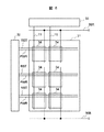
図1〜図4を用いて、本発明に係る画像表示装置の第1の実施例の構成および動作について、以下順次説明する。
図1は、携帯電話向けの有機ELディスプレイの構成図である。表示領域21には画素13がマトリクス状に配置されており、画素13には垂直方向に信号線11が、水平方向には後で詳しく説明するように、リセット線RST、第1ゲート線GT1、第2ゲート線GT2(以下、ゲート線と呼ぶ)が接続されている。信号線11の一端は信号電圧出力回路23に接続され、リセット線RST、ゲート線GT1,GT2の一端は走査回路22に接続される。
The configuration and operation of the first embodiment of the image display apparatus according to the present invention will be sequentially described below with reference to FIGS.
FIG. 1 is a configuration diagram of an organic EL display for a mobile phone.
図面を簡略化するために図1には6画素しか記載していないが、実際には画素駆動信号線15Aは図面で上部の画素に入力されており、対応する画素数は240(水平)×RGB×50(垂直)である。また画素駆動信号線15Bが対応する画素数は240(水平)×RGB×320(垂直)である。なお表示領域21内における画素は、全て同一のピッチサイズである。画素駆動信号線15Aが入力する画素も、画素駆動信号線15Bが入力する画素もみな連続して均一に配置されている。さらに、図2で示される電源線12も図1では、煩雑になるため省略されている。また表示領域21内における画素は、全て同一のガラス基板上に設けられている。
In order to simplify the drawing, only 6 pixels are shown in FIG. 1, but the pixel
次に、画素13の構成を説明する。図2は画素13の画素回路図であり、各画素13には有機EL素子1が設けられている。有機EL素子1の一端は共通電極に接続され、他端は駆動TFT3を介して電源線12に接続されている。駆動TFT3のゲート−ドレイン間には、リセットスイッチ4が接続されている。また駆動TFT3のゲートは、記憶容量5及び画素スイッチSW1を介して信号線11に、画素スイッチSW2を介して画素駆動信号線15に接続されている。なおリセットスイッチRSWはリセット線RSTにより、画素スイッチSW1はゲート線GT1により、画素スイッチSW2はゲート線GT2により、それぞれ制御される。
Next, the configuration of the
次に、本実施例の動作について図3を用いて説明する。
図3は、本実施例における画素への信号電圧書込み時の動作タイミング図である。ここで、リセット線RSTで制御されるリセットスイッチRSW、ゲート線GT1で制御される画素スイッチSW1、ゲート線GT2で制御される画素スイッチSW2は、図2に示したようにpMOSであるため、図3に示した各波形は下が各スイッチのON、上がOFFに対応している。
Next, the operation of this embodiment will be described with reference to FIG.
FIG. 3 is an operation timing chart at the time of writing a signal voltage to the pixel in this embodiment. Here, the reset switch RSW controlled by the reset line RST, the pixel switch SW1 controlled by the gate line GT1, and the pixel switch SW2 controlled by the gate line GT2 are pMOS as shown in FIG. Each waveform shown in FIG. 3 corresponds to ON of each switch at the bottom and OFF at the top.
書込みを選択された画素では、始めにゲート線GT1及びゲート線GT2の信号電圧が切り替わることによって、信号線11が記憶容量5の一端に接続される。
次いで、信号線11に映像信号電圧が入力されるとともに、リセット線RSTによってリセットスイッチRSWがONになると、駆動TFT3と有機EL素子1はリセットスイッチRSWによって入力端と出力端とが短絡させられたインバータ回路として動作する。このときこの有機EL素子1を負荷とするインバータ回路の入力電圧は、インバータ回路の論理しきい値の中点にリセットされる。
In the pixel selected for writing, the
Next, when the video signal voltage is input to the
この結果、記憶容量5の両端には、映像信号電圧とインバータ回路の論理しきい値の中点電圧が入力される。記憶容量5のこの状態は、リセット線RSTによってリセットスイッチRSWがOFFになることによって保持される。
As a result, the video signal voltage and the midpoint voltage of the logical threshold value of the inverter circuit are input to both ends of the
次いで、ゲート1線10及びゲート2線14が切り替わることによって、書込み動作時以外のタイミングでは、記憶容量5の一端には画素駆動信号線15が接続される。ここで本実施例では、画素駆動信号線15には所定の駆動電圧が入力されている。これに関して以下、図4を用いて説明する。
Next, when the
図4は、本実施例における画素駆動信号線15に印加される駆動電圧DRVの1フレーム期間(FRM)の波形である。ここでは1フレーム期間は1/60秒に設定した。図から明らかなように、画素駆動信号線15に印加される駆動電圧DRVは、画素駆動信号線15Aと画素駆動信号線15Bとで異ならせている。即ち画素駆動信号線15Aに印加されている駆動電圧DRV_15Aは一定電圧であるのに対して、画素駆動信号線15Bに印加されている駆動電圧DRV_15Bは、下に凸の一個の対称な三角波である。これによって、画素駆動信号線15Aの信号電圧が印加されている画素と、画素駆動信号線15Bの信号電圧が印加されている画素とでは、画素の発光動作に違いが生じる。
FIG. 4 shows a waveform of one frame period (FRM) of the drive voltage DRV applied to the pixel
画素駆動信号線15Aの信号電圧が印加されている画素では、駆動TFT3のゲート電圧は、先のインバータ回路の論理しきい値の中点電圧に対して、映像信号電圧と画素駆動信号線15Aに印加されている一定電圧である駆動電圧DRV_15Aの電圧差に相当する電圧が印加される。従って、有機EL素子1は映像信号電圧に対応する発光強度で次の書込み期間まで発光を続ける。
In the pixel to which the signal voltage of the pixel
これに対して画素駆動信号線15Bが印加されている画素では、駆動TFT3のゲート電圧は、画素駆動信号線15Bに印加されている下に凸の三角波駆動電圧DRV_15Bで駆動される。このとき、三角波駆動電圧DRV_15Bの値が映像信号電圧に一致した瞬間では、駆動TFT3のゲート電圧は先のインバータ回路の論理しきい値の中点電圧であるため、有機EL素子1は点灯と消灯の中間状態になる。三角波駆動電圧DRV_15Bの値が映像信号電圧よりも大きければ、インバータの出力論理はOFFであるから、有機EL素子1は点灯しない。一方、三角波駆動電圧DRV_15Bの値が映像信号電圧よりも小さければ、インバータの出力論理はONであるから、有機EL素子1は点灯することになる。
On the other hand, in the pixel to which the pixel
従って、映像信号電圧値と三角波駆動電圧の大小関係によって、有機EL素子1の1フレーム期間内の点灯時間が規定される。これにより、有機EL素子1は映像信号電圧に対応する発光期間で点灯することによって、輝度階調を実現することができる。
Accordingly, the lighting time within one frame period of the
以上のように本実施例では、2種類の画素駆動信号線15A,15Bをそれぞれ異なる画素群に配線することによって、単一の信号電圧出力回路23による同一の映像信号電圧に対しても、異なる信号−輝度特性を実現することができる。ここで、異なる画素駆動信号線15A,15Bの信号電圧が印加される2つの画素領域は、前者は主にテキスト及びアイコンを表示する領域であり、後者は自然画を含む一般の映像表示領域である。
As described above, in this embodiment, the two types of pixel
また、一定電圧である駆動電圧DRV_15Aの電圧値と、下に凸の三角波である駆動電圧DRV_15Bの形状をそれぞれ独立に調整することによって、黒の沈み方や白の輝度などを独立に調整可能であることは言うまでもない。 In addition, by independently adjusting the voltage value of the drive voltage DRV_15A, which is a constant voltage, and the shape of the drive voltage DRV_15B, which is a downwardly convex triangular wave, it is possible to independently adjust how the black sinks, white brightness, etc. Needless to say.
なお、三角波である駆動電圧DRV_15Bが印加され、有機EL素子1を映像信号電圧に対応する発光期間で点灯することによって輝度階調を実現する、画素駆動信号線15Bの信号電圧が印加されている画素群に関しては、特に「ピーク輝度」特性が実現されていることに着目するべきである。「ピーク輝度」特性とは、局所的な輝点の発光輝度を全面が白表示の場合の発光輝度よりも数倍大きくすることによって、キラリとしたきらめきを表現する特性であって、CRT(Cathode Ray Tube)で実用化されている機能である。
In addition, the drive voltage DRV_15B that is a triangular wave is applied, and the signal voltage of the pixel
上記画素群の発光は、基本的にはON及びOFFの2つの状態によって制御されるが、ここでON状態の発光輝度は、基本的に電源線12の電圧によって定まる値である。このとき、大部分の画素が発光する際には電源線12が供給する発光電流が大きくなるため、必然的に電源線12の電圧は降下する。この大部分の画素が発光する際には、有機EL素子1の発光輝度は低下する。その一方で局所的な画素が発光する際には電源線12が供給する発光電流は小さく、電源線12の電圧降下は無視できる。この局所的な画素が発光する際には、先程の有機EL素子1の発光輝度低下は生じない。このようにして、画素駆動信号線15Bの信号電圧が印加されている画素群に関しては、特に「ピーク輝度」特性が実現されるのである。これによって画素駆動信号線15Bの信号電圧が印加されている画素群は、高品位な自然画を表現することができる。
The light emission of the pixel group is basically controlled by two states, ON and OFF. Here, the light emission luminance in the ON state is basically a value determined by the voltage of the
これに対して画素駆動信号線15Aの信号電圧が印加されている画素群は、駆動TFT3のゲート電圧によって有機EL素子1の発光輝度を制御するため、数割程度の輝度変調はあるものの、基本的に「ピーク輝度」特性は存在しない。ところが画素駆動信号線15Aの信号電圧が印加されている画素群は、専らテキストやアイコンを表示するための画素であるため、「ピーク輝度」特性は無い方が好ましい。何故なら、画素駆動信号線15Bの信号電圧が印加されている画素群の自然画の映像が変わる度に、テキストやアイコンの輝度まで変化してしまうことは望ましくないからである。
このように、本実施例においては、「ピーク輝度」特性の面においても画素発光特性を最適化することができる。
On the other hand, the pixel group to which the signal voltage of the pixel driving
As described above, in this embodiment, the pixel light emission characteristic can be optimized also in terms of the “peak luminance” characteristic.
本実施例では、画素内のTFTを多結晶Siで形成したpMOSトランジスタとしたが、各制御電圧の正負を逆にすれば適宜nMOSトランジスタを用いることは可能であり、また多結晶Siに拘らずにその他の有機/無機半導体薄膜をトランジスタに用いることも可能である。 In this embodiment, the TFT in the pixel is a pMOS transistor formed of polycrystalline Si. However, if the positive and negative of each control voltage are reversed, an nMOS transistor can be used as appropriate, regardless of the polycrystalline Si. In addition, other organic / inorganic semiconductor thin films can be used for the transistor.
また発光素子としても有機EL素子に限らず、無機EL素子やFED(Field-Emission Device)など一般の発光素子を用いることができることは明らかである。 Further, the light-emitting element is not limited to the organic EL element, and it is obvious that a general light-emitting element such as an inorganic EL element or FED (Field-Emission Device) can be used.
更に、本実施例では画素群を2つのグループに分割したが、このような分割数を増やすことも当然可能である。 Further, in this embodiment, the pixel group is divided into two groups, but it is naturally possible to increase the number of such divisions.
なお、本実施例において説明した三角波を用いて有機EL素子を発光期間変調駆動する技術に関しては、特許文献1や、特許文献2などに詳しく記載されている。
Note that the technology for driving the organic EL element to be modulated during the light emission period using the triangular wave described in the present embodiment is described in detail in
以下図5を用いて、本発明に係る画像表示装置の第2の実施例に関して説明する。
本実施例において、有機ELディスプレイの構成、画素回路やその基本的な動作方法は、既に述べた第1の実施例と殆ど同様である。第1の実施例との差異は、画素駆動信号線15に印加される駆動電圧DRVの1フレーム期間の波形であるため、ここでは以下これに関してのみ図5を用いて説明する。
Hereinafter, a second embodiment of the image display apparatus according to the present invention will be described with reference to FIG.
In this embodiment, the configuration of the organic EL display, the pixel circuit, and the basic operation method thereof are almost the same as those of the first embodiment already described. Since the difference from the first embodiment is the waveform of the drive voltage DRV applied to the pixel
図5は、本実施例における、画素駆動信号線15に印加される駆動電圧DRVの1フレーム期間(1FRM)の波形である。ここでも1フレーム期間は1/60秒に設定した。図から明らかなように、画素駆動信号線15に印加される駆動電圧DRVは、第1の実施例における画素駆動電圧DRV_15Aに変えて画素駆動電圧DRV_15Cと、第1の実施例における画素駆動電圧DRV_15Bに変えて画素駆動電圧DRV_15Dのように定められている。
FIG. 5 shows the waveform of one frame period (1FRM) of the drive voltage DRV applied to the pixel
ここで、画素駆動信号線15Aに印加されている駆動電圧DRV_15Cは直線で構成された三角波であるのに対して、画素駆動信号線15Bに印加されている駆動電圧DRV_15Dは上に凸の曲線で構成された三角波である。これによって、画素駆動信号線15Aの駆動電圧が印加されている画素と、画素駆動信号線15Bの駆動電圧が印加されている画素とでは、画素の発光動作に違いが生じる。
Here, the drive voltage DRV_15C applied to the pixel
本実施例の場合は、全画素の有機EL素子1が映像信号電圧に対応する発光期間で点灯することによって輝度階調を実現するが、画素駆動信号線15Aの駆動電圧DRV_15Cが入力されている画素と、画素駆動信号線15Bの駆動電圧DRV_15Dが入力されている画素とでは、駆動電圧DRVの波形が異なるために、そのガンマ特性が異なってくる。これによって本実施例でも、2種類の画素駆動信号線15をそれぞれ異なる画素群に配線することによって、単一の信号電圧出力回路23による同一の映像信号電圧に対しても、異なる信号−輝度特性を実現することができる。
In the present embodiment, the
本実施例でも異なる画素駆動信号線15A,15Bの駆動電圧が入力される2つの画素領域は、前者は主にテキスト及びアイコンを表示する領域であり、後者は自然画を含む一般の映像表示領域であり、後者の方により強いガンマ特性が与えられている。また、駆動電圧DRV_15C,DRV_15Dの形状をそれぞれ独立に調整することによって、ガンマ特性のみならず黒の沈み方や白の輝度などを独立に調整可能であることは言うまでもない。
Also in this embodiment, the two pixel regions to which the drive voltages of the different pixel
図6〜図8を用いて、本発明に係る画像表示装置の第3の実施例に関して説明する。
図6は、携帯端末向けの有機ELディスプレイの構成図である。表示領域31には画素34がマトリクス状に配置されており、画素34には垂直方向に信号線11が、水平方向には後で詳しく説明するように、リセット線RST、電源制御線8が接続されている。信号線11の一端は信号電圧出力回路33に、リセット線RSTと、電源制御線8の一端は走査回路32に接続される。ここで図6に示されているように、画素は電源線35Aが接続される画素群と、電源線35Bが接続される画素群とから構成されており、電源線35Aと電源線35Bには異なる電源電圧が入力されている。
A third embodiment of the image display apparatus according to the present invention will be described with reference to FIGS.
FIG. 6 is a configuration diagram of an organic EL display for a portable terminal.
図面を簡略化するために図6には6画素しか記載していないが、実際にはVGA(640×480)の画素が設けられている。電源線35Aの入力する画素数は640(水平)×RGB×380(垂直)、電源線35Bの入力する画素数は640(水平)×RGB×100(垂直)である。なお、表示領域31内における画素は全て同一のピッチサイズであり、電源線35Aが接続される画素も、電源線35Bが接続される画素も、みな連続して均一に配置されている。また、表示領域31内における画素は全て同一のガラス基板上に設けられている。
In order to simplify the drawing, only 6 pixels are shown in FIG. 6, but in reality, VGA (640 × 480) pixels are provided. The number of pixels input to the
次に、画素34の構成を説明する。
図7は、画素34の画素回路図である。各画素34には有機EL素子1が設けられており、有機EL素子1の一端は共通電極に接続され、他端は電源制御スイッチ2及び駆動TFT3を介して電源線35に接続されている。駆動TFT3のゲート−ドレイン間にはリセットスイッチRSWが接続されている。また、駆動TFT3のゲートは記憶容量5を介して信号線11に接続されている。なお、リセットスイッチRSWはリセット線RST、電源制御スイッチ2は電源制御線PWRにより制御される。
Next, the configuration of the
FIG. 7 is a pixel circuit diagram of the
次に、本実施例の動作について図8を用いて説明する。
図8は、本実施例における画素の動作タイミング図であり、前半のデータ入力期間DAT_INが画素への信号電圧書込み、後半のILMI期間が画素の階調発光期間に相当している。ここで、上記リセットスイッチRSWと電源制御スイッチ2は、図7に示したようにpMOSであるため、図8に示した各波形は下が各スイッチのON、上がOFFに対応している。
Next, the operation of this embodiment will be described with reference to FIG.
FIG. 8 is an operation timing chart of the pixel in this embodiment. The first data input period DAT_IN corresponds to the signal voltage writing to the pixel, and the second ILMI period corresponds to the gradation light emission period of the pixel. Here, since the reset switch RSW and the
書込みを選択された画素では、始めに電源制御線PWRが切り替わることによって、有機EL素子1が駆動TFT3に接続される。更に、リセット線RSTによってリセットスイッチRSWがONになると、リセットスイッチRSWによってダイオード接続された駆動TFT3と有機EL素子1は、電源制御スイッチ2によって電源線35に接続され電流が流れる。
In the pixel selected to be written, the
次いで、電源制御線PWRがターンオフして電源制御スイッチ2がOFFすると、駆動TFT3のドレイン端が閾値電圧Vthになった時点で、駆動TFT3はターンオフする。このとき信号線11には、映像信号電圧データDAT(IMG)が印加されており、この映像信号電圧データDAT(IMG)と上記閾値電圧Vthの差が、記憶容量5に入力される。
Next, when the power supply control line PWR is turned off and the power
次いで、リセット線RSTによってリセットスイッチRSWがOFFになった時点で、この画素への信号電圧書込みは終了する。このようにして、前半のデータ入力期間DAT_INでは、各画素への信号電圧書込みが順次行われる。 Next, when the reset switch RSW is turned off by the reset line RST, the signal voltage writing to the pixel is finished. In this manner, signal voltage writing to each pixel is sequentially performed in the first half data input period DAT_IN.
画素への書込みが完了すると、後半のILMI期間が画素の階調発光期間である。この期間では、図8に示したように、信号線11には下に凸の三角波電圧データDAT(▽)が入力される。このとき信号線11の電圧値DAT(▽)が、先に書込まれた映像信号電圧データDAT(IMG)に一致した瞬間では、駆動TFT3のゲート電圧は先の閾値電圧Vthであるため、有機EL素子1は点灯と消灯の中間状態になる。信号線11の三角波データDAT(▽)の電圧値が映像信号電圧データDAT(IMG)よりも大きければ、駆動TFTはターンオフするので有機EL素子1は点灯せず、信号線11の三角波データDAT(▽)の電圧値が映像信号電圧データDAT(IMG)よりも小さければ、駆動TFTはターンオンするので有機EL素子1は点灯することになる。
When writing to the pixel is completed, the latter half of the ILMI period is the gradation light emission period of the pixel. In this period, as shown in FIG. 8, the triangular wave voltage data DAT (▽) convex downward is input to the
従って、あらかじめ書込まれた映像信号電圧値DAT(IMG)と信号線11に印加される三角波電圧DAT(▽)の大小関係によって、有機EL素子1の1フレーム期間内の点灯時間が規定される。すなわち、有機EL素子1は映像信号電圧に対応する発光期間で点灯することによって、輝度階調を実現することができる。
Accordingly, the lighting time within one frame period of the
このとき図6に示したように、画素は電源線35Aが接続される画素群と、電源線35Bが接続される画素群とから構成されており、電源線35Aと電源線35Bには異なる電源電圧が入力されている。このため有機EL素子1がONした際の発光輝度には、電源線35Aが接続される画素群と、電源線35Bが接続される画素群とでは違いが生じる。ここで異なる電源線35A,35Bが接続される2つの画素領域は、前者は自然画を含む一般の映像表示領域であり、後者は主にテキストを表示する文字情報領域である。
At this time, as shown in FIG. 6, the pixel is composed of a pixel group to which the
このとき、電源線35Aには比較的高電圧を所定の出力インピーダンスを介して与えることにより、電源線35Aが接続される画素群はピーク輝度を含む高輝度の表示を可能としている。また電源線35Bには比較的低電圧を与えることにより、電源線35Bが接続される画素群は、ピーク輝度の殆どない比較的低輝度の表示を可能とした。
At this time, by applying a relatively high voltage to the
なお、本実施例においては、更にRGBの表示色別にこのように電源線35を複数系統持たせることによって、更にきめの細かい画質制御が可能である。また、電源線35に印加する電源電圧値を映像によってリアルタイムに制御することで、更に好適な画質制御を行うことも可能である。
In the present embodiment, finer image quality control can be achieved by providing a plurality of
図9を用いて、本発明に係る画像表示装置の第4の実施例に関して説明する。
図9は、メイン(主)及びサブ(従)パネルを有する携帯電話向けの有機ELディスプレイの構成図である。表示領域21及び表示領域21Aはそれぞれメイン(主)及びサブ(従)パネルに相当し、それぞれ画素13がマトリクス状に配置されている。画素13には垂直方向に信号線11が、水平方向に第1の実施例と同様に、リセット線RST、第1ゲート線GT1、第2ゲート線GT2が接続されている。表示領域21及び表示領域21Aとも信号線11の一端は信号電圧出力回路23に共通に接続され、リセット線RST、ゲート線GT1,GT2の一端は表示領域21及び表示領域21Aでそれぞれ走査回路22及び22Aに接続される。
The fourth embodiment of the image display apparatus according to the present invention will be described with reference to FIG.
FIG. 9 is a configuration diagram of an organic EL display for a mobile phone having a main (main) and sub (sub) panels. The
図面を簡略化するために図9の表示領域21には6画素、表示領域21Aには4画素しか記載していないが、実際には表示領域21に対応する画素数は240(水平)×RGB×320(垂直)であり、表示領域21Aに対応する画素数は160(水平)×RGB×120(垂直)である。このために記載していない右端では、表示領域21における信号線11は80本余っていることになる。ここで画素駆動信号線15Cは表示領域21に対応する画素に接続されており、画素駆動信号線15Dは表示領域21Aに対応する画素に接続されている。なお、表示領域21内における画素は全て同一のピッチサイズであり、表示領域21A内における画素は全て同一のピッチサイズであるが、表示領域21と表示領域21Aの画素のピッチサイズは異なっている。また、表示領域21内における画素は全て同一のガラス基板上に、表示領域21A内における画素は全て同一のガラス基板上に設けられているが、表示領域21と表示領域21Aのガラス基板は異なっている。
In order to simplify the drawing, only 6 pixels are shown in the
ここで本実施例は、メイン(主)及びサブ(従)パネルのガラス基板が異なっていることを除けば、画素駆動信号線15C,15Dを画素駆動信号線15B、15Aと読み替えた際の第1の実施例と同様な動作、特徴を有する。
In this embodiment, except that the glass substrates of the main (main) and sub (secondary) panels are different, the pixel driving
携帯電話のメインパネルには自然画を含めて一般の映像が表示されるが、サブパネルに表示されるのはテキストやアイコンが多いという特徴がある。そこで、本実施例を携帯電話に適用すれば、メインパネルとサブパネルの信号−輝度特性をそれぞれ最適化させることによって、携帯電話のメインパネルの高画質化と、サブパネルに表示される文字の認識し易さの向上とを両立させることができる。 A general picture including a natural picture is displayed on the main panel of the mobile phone, but the sub-panel is characterized by many texts and icons. Therefore, if this embodiment is applied to a mobile phone, by optimizing the signal-luminance characteristics of the main panel and sub panel, respectively, the image quality of the main panel of the mobile phone can be improved and the characters displayed on the sub panel can be recognized. It is possible to achieve both improvement in ease.
図10を用いて、本発明に係る画像表示装置の第5の実施例に関して説明する。
図10は、携帯電話向けの有機ELディスプレイの構成図である。表示領域21には画素13がマトリクス状に配置されており、画素13には垂直方向に信号線11が、水平方向に第1の実施例と同様に、リセット線RST、第1ゲート線GT1、第2ゲート線GT2が接続されている。信号線11の一端は信号電圧出力回路23に、リセット線RST、ゲートGT1,GT2の一端は走査回路22に接続されている。図面を簡略化するために図1には6画素しか記載していないが、実際の画素数は240(水平)×RGB×320(垂直)である。なお、表示領域21内における画素は全て同一のピッチサイズである。また、表示領域21内における画素は全て同一のガラス基板上に設けられている。
A fifth embodiment of the image display apparatus according to the present invention will be described with reference to FIG.
FIG. 10 is a configuration diagram of an organic EL display for a mobile phone.
ここで、画素駆動信号線15は画素の一端で画素駆動信号選択回路40に接続され、画素駆動信号選択回路40内で画素駆動信号線15A,15Bに選択的に接続される。
Here, the pixel
本実施例は、画素駆動信号選択回路40によって、画素駆動信号線15を行毎に画素駆動信号線15Aまたは、15Bに選択的に接続することを除けば、第1の実施例と同様な動作、特徴を有する。
The present embodiment operates in the same manner as the first embodiment except that the pixel
更に、本実施例は画素駆動信号選択回路40を有するため、ディスプレイに表示する映像信号によって各画素の信号−輝度表示特性を動的に変更することが可能であるという特徴をもつ。
Further, since the present embodiment includes the pixel drive
図11を用いて、本発明に係る画像表示装置の第6の実施例に関して説明する。
図11は、TV画像表示装置100の構成図である。地上波デジタル信号等を受信する無線インターフェース(I/F)回路102には、圧縮された画像データ等が外部から無線データとして入力され、無線I/F回路102の出力はI/O(Input/Output)回路を介してデータバス108に接続される。データバス108には、この他にマイクロプロセサ(MPU)、表示パネルコントローラ106、フレームメモリ(MEM)等が接続されている。更に、表示パネルコントローラ106の出力は有機EL表示パネル101に入力されている。画像表示端末100には、更に電源PWSが設けられている。なお、ここで有機EL表示パネル101は、先に延べた第5の実施例と同一の構成および動作を有しているので、その内部の構成及び動作の記載はここでは省略する。
A sixth embodiment of the image display apparatus according to the present invention will be described with reference to FIG.
FIG. 11 is a configuration diagram of the TV
本実施例の動作を説明する。始めに、無線I/F回路102は命令に応じて圧縮された画像データを外部から取り込み、この画像データをI/O回路を介してMPU及びフレームメモリに転送する。MPU104はユーザからの命令操作を受けて、必要に応じて画像表示端末100全体を駆動し、圧縮された画像データのデコードや信号処理、および情報表示を行う。なお、信号処理された画像データは、フレームメモリに一時的に蓄積が可能である。
The operation of this embodiment will be described. First, the wireless I /
ここで、MPU104が表示命令を出した場合には、その指示に従ってフレームメモリMEMから表示パネルコントローラ106を介して有機EL表示パネル101に画像データが入力され、有機EL表示パネル101は入力された画像データをリアルタイムで表示する。このとき表示パネルコントローラ106は、同時に画像を表示するために必要な所定のタイミングパルスを出力すると共に、表示画像データに合わせてどの画素群が異なる発光輝度を出力するかの選択を映像内容によって決定し、画素駆動信号選択回路40を所定のアルゴリズムで制御する。なお有機EL表示パネル101がこれらの信号を用いて、入力された画像データをリアルタイムで表示することに関しては、第5の実施例で述べたとおりである。なお、ここで電源PWSには、二次電池が含まれており、これらの画像表示端末100全体を駆動する電力を供給する。
Here, when the MPU 104 issues a display command, image data is input from the frame memory MEM to the organic
本実施例によれば、高画質表示が可能である画像表示端末100を提供することができる。なお、本実施例では画像表示デバイスとして、第5の実施例で説明した有機EL表示パネルを用いたが、これ以外にその他の本発明の実施例に記載されたような種々の表示パネルを用いることが可能であることは明らかである。但し、この場合は有機EL表示パネルの構造に応じた若干の回路変更が必要になることは言うまでもない。
According to the present embodiment, it is possible to provide the
1…有機EL素子、3…駆動TFT、5…記憶容量、11…信号線、13,34…画素、15,15A,15B…画素駆動信号線、21,21A,31…表示領域、22,32…走査回路、23,33…信号電圧出力回路、35A,35B…電源線、40…画素駆動信号選択回路、100…画像表示端末、101…有機EL表示パネル、102…無線インターフェース(I/F)回路、DAT(IMG)…映像信号電圧データ、DAT(▽)…下に凸の三角波電圧データ、DRV,DRV_15A〜15D…駆動電圧、GT1…第1ゲート線、GT2…第2ゲート線、MEM…フレームメモリ、MPU…マイクロプロセサ、PWR…電源制御線、PWS…電源、RST…リセット線、RSW…リセットスイッチ、SW1,SW2…画素スイッチ。
DESCRIPTION OF
Claims (14)
前記映像信号電圧によって輝度が制御される発光素子及び該発光素子の輝度制御部を有する画素と、
複数の前記画素が配列された表示部とを有する画像表示装置であって、
前記画素は該発光素子と、前記発光素子を駆動するためにその一端に接続された駆動用トランジスタと、前記駆動用トランジスタのドレイン端子とゲート端子間に接続されたリセットトランジスタと、前記駆動用トランジスタのゲート端子と信号線との間に設けられ
た映像信号蓄積用コンデンサを有し、
前記映像信号電圧発生回路が出力した同一の前記映像信号電圧値に対して、発光スペクトルが実質的に等しく、かつ発光輝度が異なるように画素を駆動するために、該発光素子の発光制御期間内に、前記駆動用トランジスタのゲート端子と接続されていない方の前記映像信号蓄積用コンデンサの一端に対して印加する駆動電圧信号を、画素によって異ならせるようにしたことを特徴とする画像表示装置。 A video signal voltage generation circuit for outputting a video signal voltage;
A light emitting element whose luminance is controlled by the video signal voltage and a pixel having a luminance control unit of the light emitting element;
An image display device having a display unit in which a plurality of the pixels are arranged,
The pixel includes the light emitting element, a driving transistor connected to one end of the pixel for driving the light emitting element, a reset transistor connected between a drain terminal and a gate terminal of the driving transistor, and the driving transistor. A video signal storage capacitor provided between the gate terminal and the signal line,
In order to drive the pixels so that the light emission spectrum is substantially equal and the light emission luminance is different from the same video signal voltage value output by the video signal voltage generation circuit, In addition, the drive voltage signal applied to one end of the video signal storage capacitor that is not connected to the gate terminal of the drive transistor is made different for each pixel.
前記映像信号電圧によって輝度が制御される発光素子と該発光素子の輝度制御部を有する画素と、
複数の前記画素が配列された表示部とを有する画像表示装置であって、
前記画素は該発光素子と、前記発光素子を駆動するためにその一端に接続された駆動用トランジスタと、前記駆動用トランジスタのドレイン端子とゲート端子間に接続されたリセットトランジスタと、前記駆動用トランジスタのゲート端子と信号線との間に設けられた映像信号蓄積用コンデンサを有し、
同一の前記映像信号電圧発生回路が出力した同一の前記映像信号電圧値に対して、発光スペクトルが実質的に等しく、かつ発光輝度が異なるように画素を駆動するために、該発光素子の発光制御期間内に、前記駆動用トランジスタのゲート端子と接続されていない方の前記映像信号蓄積用コンデンサの一端に対して印加する駆動電圧信号を、画素によって異ならせるようにし、前記映像信号から画素の前記発光輝度特性を制御する制御部を有することを特徴とする画像表示装置。 A video signal voltage generation circuit for outputting a video signal voltage;
A light-emitting element whose luminance is controlled by the video signal voltage, and a pixel having a luminance control unit of the light-emitting element;
An image display device having a display unit in which a plurality of the pixels are arranged,
The pixel includes the light emitting element, a driving transistor connected to one end of the pixel for driving the light emitting element, a reset transistor connected between a drain terminal and a gate terminal of the driving transistor, and the driving transistor. A video signal storage capacitor provided between the gate terminal and the signal line,
In order to drive the pixels so that the emission spectrum is substantially equal and the emission luminance is different with respect to the same video signal voltage value output by the same video signal voltage generation circuit, light emission control of the light emitting element is performed. A drive voltage signal applied to one end of the video signal storage capacitor that is not connected to the gate terminal of the drive transistor within the period is made to vary depending on the pixel, and images display you further comprising a control unit for controlling the light emission luminance characteristics.
Priority Applications (5)
| Application Number | Priority Date | Filing Date | Title |
|---|---|---|---|
| JP2004305241A JP4846999B2 (en) | 2004-10-20 | 2004-10-20 | Image display device |
| TW094132314A TW200623010A (en) | 2004-10-20 | 2005-09-19 | Image display apparatus |
| US11/250,442 US8279203B2 (en) | 2004-10-20 | 2005-10-17 | Image display device |
| KR1020050098431A KR101217931B1 (en) | 2004-10-20 | 2005-10-19 | image display device |
| CN200510116433A CN100592362C (en) | 2004-10-20 | 2005-10-20 | Image display device |
Applications Claiming Priority (1)
| Application Number | Priority Date | Filing Date | Title |
|---|---|---|---|
| JP2004305241A JP4846999B2 (en) | 2004-10-20 | 2004-10-20 | Image display device |
Publications (2)
| Publication Number | Publication Date |
|---|---|
| JP2006119242A JP2006119242A (en) | 2006-05-11 |
| JP4846999B2 true JP4846999B2 (en) | 2011-12-28 |
Family
ID=36180258
Family Applications (1)
| Application Number | Title | Priority Date | Filing Date |
|---|---|---|---|
| JP2004305241A Expired - Lifetime JP4846999B2 (en) | 2004-10-20 | 2004-10-20 | Image display device |
Country Status (5)
| Country | Link |
|---|---|
| US (1) | US8279203B2 (en) |
| JP (1) | JP4846999B2 (en) |
| KR (1) | KR101217931B1 (en) |
| CN (1) | CN100592362C (en) |
| TW (1) | TW200623010A (en) |
Families Citing this family (21)
| Publication number | Priority date | Publication date | Assignee | Title |
|---|---|---|---|---|
| WO2006059737A1 (en) * | 2004-11-30 | 2006-06-08 | Semiconductor Energy Laboratory Co., Ltd. | Display device and driving method thereof, semiconductor device, and electronic apparatus |
| US7646367B2 (en) | 2005-01-21 | 2010-01-12 | Semiconductor Energy Laboratory Co., Ltd. | Semiconductor device, display device and electronic apparatus |
| JP2007298779A (en) * | 2006-04-28 | 2007-11-15 | Sony Corp | Character emphasis control device, display device, emphasis display control method, and computer program |
| CN101405785B (en) * | 2006-05-30 | 2011-08-17 | 夏普株式会社 | Current Driven Display Device |
| JP4259592B2 (en) | 2006-09-13 | 2009-04-30 | セイコーエプソン株式会社 | Electro-optical device and electronic apparatus |
| JP5342111B2 (en) * | 2007-03-09 | 2013-11-13 | 株式会社ジャパンディスプレイ | Organic EL display device |
| KR20080086747A (en) | 2007-03-23 | 2008-09-26 | 삼성에스디아이 주식회사 | Organic electroluminescent display and driving method thereof |
| JP2009075231A (en) * | 2007-09-19 | 2009-04-09 | Hitachi Displays Ltd | Image display device |
| DE102007052671B4 (en) * | 2007-11-05 | 2012-11-08 | Airbus Operations Gmbh | Display module for displaying passenger-specific display information |
| FR2931296B1 (en) * | 2008-05-13 | 2013-04-26 | Commissariat Energie Atomique | CONTROL CIRCUIT OF A PIXEL WITH VARIABLE CHROMATIC COORDINATES |
| WO2010143612A1 (en) | 2009-06-12 | 2010-12-16 | シャープ株式会社 | Pixel circuit and display device |
| WO2010143613A1 (en) * | 2009-06-12 | 2010-12-16 | シャープ株式会社 | Pixel circuit and display device |
| JP2011013574A (en) * | 2009-07-03 | 2011-01-20 | Hitachi Displays Ltd | Image display device |
| JP2011039453A (en) * | 2009-08-18 | 2011-02-24 | Hitachi Displays Ltd | Light emission element display device |
| JP5655371B2 (en) * | 2010-05-26 | 2015-01-21 | セイコーエプソン株式会社 | Electronic device and driving method thereof |
| JP5646925B2 (en) * | 2010-09-08 | 2014-12-24 | 株式会社ジャパンディスプレイ | Image display device and driving method thereof |
| KR102000207B1 (en) * | 2012-08-07 | 2019-07-16 | 삼성디스플레이 주식회사 | Organic Light Emitting Transistor and Organic Light Emitting display apparatus |
| KR102249910B1 (en) * | 2014-05-23 | 2021-05-10 | 삼성전자 주식회사 | Electronic apparatus and ouput characteristic controlling method thereof |
| KR102670088B1 (en) | 2016-05-02 | 2024-05-28 | 삼성디스플레이 주식회사 | Display Device and Driving Method Thereof |
| US12236886B2 (en) | 2020-11-27 | 2025-02-25 | Chengdu Boe Optoelectronics Technology Co., Ltd. | Pixel circuit and driving method thereof, display substrate and display device |
| US11721286B2 (en) * | 2020-11-27 | 2023-08-08 | Chengdu Boe Optoelectronics Technology Co., Ltd. | Pixel circuit and driving method thereof, display substrate and display device |
Family Cites Families (11)
| Publication number | Priority date | Publication date | Assignee | Title |
|---|---|---|---|---|
| GB2313224A (en) * | 1996-05-17 | 1997-11-19 | Sharp Kk | Ferroelectric liquid crystal device |
| TW540251B (en) * | 1999-09-24 | 2003-07-01 | Semiconductor Energy Lab | EL display device and method for driving the same |
| JP4982014B2 (en) * | 2001-06-21 | 2012-07-25 | 株式会社日立製作所 | Image display device |
| JP3899886B2 (en) * | 2001-10-10 | 2007-03-28 | 株式会社日立製作所 | Image display device |
| JP3658362B2 (en) * | 2001-11-08 | 2005-06-08 | キヤノン株式会社 | Video display device and control method thereof |
| JP2003280587A (en) * | 2002-01-18 | 2003-10-02 | Semiconductor Energy Lab Co Ltd | Display device, and display module and electronic apparatus using the same |
| JP2003308042A (en) * | 2002-04-17 | 2003-10-31 | Hitachi Ltd | Image display device |
| JP2003330422A (en) * | 2002-05-17 | 2003-11-19 | Hitachi Ltd | Image display device |
| JP3707484B2 (en) * | 2002-11-27 | 2005-10-19 | セイコーエプソン株式会社 | Electro-optical device, driving method of electro-optical device, and electronic apparatus |
| KR101179155B1 (en) * | 2002-12-27 | 2012-09-07 | 가부시키가이샤 한도오따이 에네루기 켄큐쇼 | Display device |
| JP2004240235A (en) * | 2003-02-07 | 2004-08-26 | Hitachi Ltd | LSI for display device |
-
2004
- 2004-10-20 JP JP2004305241A patent/JP4846999B2/en not_active Expired - Lifetime
-
2005
- 2005-09-19 TW TW094132314A patent/TW200623010A/en not_active IP Right Cessation
- 2005-10-17 US US11/250,442 patent/US8279203B2/en active Active
- 2005-10-19 KR KR1020050098431A patent/KR101217931B1/en not_active Expired - Lifetime
- 2005-10-20 CN CN200510116433A patent/CN100592362C/en not_active Expired - Lifetime
Also Published As
| Publication number | Publication date |
|---|---|
| TW200623010A (en) | 2006-07-01 |
| KR20060054105A (en) | 2006-05-22 |
| KR101217931B1 (en) | 2013-01-02 |
| CN100592362C (en) | 2010-02-24 |
| US8279203B2 (en) | 2012-10-02 |
| CN1770244A (en) | 2006-05-10 |
| JP2006119242A (en) | 2006-05-11 |
| US20060082566A1 (en) | 2006-04-20 |
| TWI316220B (en) | 2009-10-21 |
Similar Documents
| Publication | Publication Date | Title |
|---|---|---|
| JP4846999B2 (en) | Image display device | |
| JP4055679B2 (en) | Electro-optical device, driving method of electro-optical device, and electronic apparatus | |
| TW556349B (en) | Image display equipment | |
| CN100476938C (en) | Organic EL device, driving method thereof, and electronic equipment | |
| JP5081374B2 (en) | Image display device | |
| CN112863434B (en) | Control method and control device | |
| CN102376244A (en) | Displaying apparatus | |
| JP2012047894A (en) | Display device | |
| JPWO2009141914A1 (en) | Active matrix display device | |
| CN100552761C (en) | Image display device | |
| JP2007293264A (en) | Electro-optical device, driving method thereof, and electronic apparatus | |
| JP4596176B2 (en) | Image display device | |
| KR20190081830A (en) | organic light emitting display device | |
| JP2008304573A (en) | Display device | |
| KR102894298B1 (en) | Display device, display device driving method and controller | |
| JP5094929B2 (en) | Image display device and driving method of image display device | |
| JP4049191B2 (en) | Image display device | |
| JP4079198B2 (en) | Image display apparatus and driving method thereof | |
| JP4049190B2 (en) | Image display apparatus and driving method thereof | |
| JP2011102930A (en) | Display device, method for driving the same, and electronic equipment | |
| JP2010113231A (en) | Display device and driving method of the same, and electronic equipment | |
| JP2007011101A (en) | Electro-optical device and electronic apparatus | |
| KR102390477B1 (en) | Organic Light Emitting Diode display device and method for driving the same | |
| JP4353300B2 (en) | Image display apparatus and driving method thereof | |
| JP2008304494A (en) | Display device |
Legal Events
| Date | Code | Title | Description |
|---|---|---|---|
| A621 | Written request for application examination |
Free format text: JAPANESE INTERMEDIATE CODE: A621 Effective date: 20070316 |
|
| RD02 | Notification of acceptance of power of attorney |
Free format text: JAPANESE INTERMEDIATE CODE: A7422 Effective date: 20070316 |
|
| A977 | Report on retrieval |
Free format text: JAPANESE INTERMEDIATE CODE: A971007 Effective date: 20100818 |
|
| A131 | Notification of reasons for refusal |
Free format text: JAPANESE INTERMEDIATE CODE: A131 Effective date: 20100831 |
|
| A521 | Request for written amendment filed |
Free format text: JAPANESE INTERMEDIATE CODE: A523 Effective date: 20101021 |
|
| A711 | Notification of change in applicant |
Free format text: JAPANESE INTERMEDIATE CODE: A712 Effective date: 20110218 |
|
| RD03 | Notification of appointment of power of attorney |
Free format text: JAPANESE INTERMEDIATE CODE: A7423 Effective date: 20110218 |
|
| A131 | Notification of reasons for refusal |
Free format text: JAPANESE INTERMEDIATE CODE: A131 Effective date: 20110510 |
|
| A521 | Request for written amendment filed |
Free format text: JAPANESE INTERMEDIATE CODE: A523 Effective date: 20110706 |
|
| TRDD | Decision of grant or rejection written | ||
| A01 | Written decision to grant a patent or to grant a registration (utility model) |
Free format text: JAPANESE INTERMEDIATE CODE: A01 Effective date: 20110927 |
|
| A01 | Written decision to grant a patent or to grant a registration (utility model) |
Free format text: JAPANESE INTERMEDIATE CODE: A01 |
|
| A61 | First payment of annual fees (during grant procedure) |
Free format text: JAPANESE INTERMEDIATE CODE: A61 Effective date: 20111013 |
|
| FPAY | Renewal fee payment (event date is renewal date of database) |
Free format text: PAYMENT UNTIL: 20141021 Year of fee payment: 3 |
|
| R150 | Certificate of patent or registration of utility model |
Ref document number: 4846999 Country of ref document: JP Free format text: JAPANESE INTERMEDIATE CODE: R150 Free format text: JAPANESE INTERMEDIATE CODE: R150 |
|
| R250 | Receipt of annual fees |
Free format text: JAPANESE INTERMEDIATE CODE: R250 |
|
| R250 | Receipt of annual fees |
Free format text: JAPANESE INTERMEDIATE CODE: R250 |
|
| R250 | Receipt of annual fees |
Free format text: JAPANESE INTERMEDIATE CODE: R250 |
|
| R250 | Receipt of annual fees |
Free format text: JAPANESE INTERMEDIATE CODE: R250 |
|
| R250 | Receipt of annual fees |
Free format text: JAPANESE INTERMEDIATE CODE: R250 |
|
| S531 | Written request for registration of change of domicile |
Free format text: JAPANESE INTERMEDIATE CODE: R313531 |
|
| S533 | Written request for registration of change of name |
Free format text: JAPANESE INTERMEDIATE CODE: R313533 |
|
| S111 | Request for change of ownership or part of ownership |
Free format text: JAPANESE INTERMEDIATE CODE: R313113 |
|
| R350 | Written notification of registration of transfer |
Free format text: JAPANESE INTERMEDIATE CODE: R350 |
|
| R350 | Written notification of registration of transfer |
Free format text: JAPANESE INTERMEDIATE CODE: R350 |
|
| R250 | Receipt of annual fees |
Free format text: JAPANESE INTERMEDIATE CODE: R250 |
|
| R250 | Receipt of annual fees |
Free format text: JAPANESE INTERMEDIATE CODE: R250 |
|
| R250 | Receipt of annual fees |
Free format text: JAPANESE INTERMEDIATE CODE: R250 |
|
| R250 | Receipt of annual fees |
Free format text: JAPANESE INTERMEDIATE CODE: R250 |
|
| R250 | Receipt of annual fees |
Free format text: JAPANESE INTERMEDIATE CODE: R250 |
|
| EXPY | Cancellation because of completion of term |