KR20150002627A - Light-emitting semiconductor component and method for producing a light-emitting semiconductor component - Google Patents
Light-emitting semiconductor component and method for producing a light-emitting semiconductor component Download PDFInfo
- Publication number
- KR20150002627A KR20150002627A KR1020147027027A KR20147027027A KR20150002627A KR 20150002627 A KR20150002627 A KR 20150002627A KR 1020147027027 A KR1020147027027 A KR 1020147027027A KR 20147027027 A KR20147027027 A KR 20147027027A KR 20150002627 A KR20150002627 A KR 20150002627A
- Authority
- KR
- South Korea
- Prior art keywords
- light emitting
- semiconductor chip
- semiconductor component
- thermal
- semiconductor
- Prior art date
- Legal status (The legal status is an assumption and is not a legal conclusion. Google has not performed a legal analysis and makes no representation as to the accuracy of the status listed.)
- Withdrawn
Links
Images


Classifications
-
- H—ELECTRICITY
- H10—SEMICONDUCTOR DEVICES; ELECTRIC SOLID-STATE DEVICES NOT OTHERWISE PROVIDED FOR
- H10H—INORGANIC LIGHT-EMITTING SEMICONDUCTOR DEVICES HAVING POTENTIAL BARRIERS
- H10H20/00—Individual inorganic light-emitting semiconductor devices having potential barriers, e.g. light-emitting diodes [LED]
- H10H20/80—Constructional details
- H10H20/85—Packages
- H10H20/852—Encapsulations
- H10H20/853—Encapsulations characterised by their shape
-
- H—ELECTRICITY
- H10—SEMICONDUCTOR DEVICES; ELECTRIC SOLID-STATE DEVICES NOT OTHERWISE PROVIDED FOR
- H10H—INORGANIC LIGHT-EMITTING SEMICONDUCTOR DEVICES HAVING POTENTIAL BARRIERS
- H10H20/00—Individual inorganic light-emitting semiconductor devices having potential barriers, e.g. light-emitting diodes [LED]
- H10H20/01—Manufacture or treatment
-
- H—ELECTRICITY
- H10—SEMICONDUCTOR DEVICES; ELECTRIC SOLID-STATE DEVICES NOT OTHERWISE PROVIDED FOR
- H10H—INORGANIC LIGHT-EMITTING SEMICONDUCTOR DEVICES HAVING POTENTIAL BARRIERS
- H10H20/00—Individual inorganic light-emitting semiconductor devices having potential barriers, e.g. light-emitting diodes [LED]
- H10H20/80—Constructional details
- H10H20/85—Packages
- H10H20/857—Interconnections, e.g. lead-frames, bond wires or solder balls
-
- H—ELECTRICITY
- H10—SEMICONDUCTOR DEVICES; ELECTRIC SOLID-STATE DEVICES NOT OTHERWISE PROVIDED FOR
- H10H—INORGANIC LIGHT-EMITTING SEMICONDUCTOR DEVICES HAVING POTENTIAL BARRIERS
- H10H20/00—Individual inorganic light-emitting semiconductor devices having potential barriers, e.g. light-emitting diodes [LED]
- H10H20/80—Constructional details
- H10H20/85—Packages
- H10H20/858—Means for heat extraction or cooling
- H10H20/8582—Means for heat extraction or cooling characterised by their shape
-
- H—ELECTRICITY
- H10—SEMICONDUCTOR DEVICES; ELECTRIC SOLID-STATE DEVICES NOT OTHERWISE PROVIDED FOR
- H10H—INORGANIC LIGHT-EMITTING SEMICONDUCTOR DEVICES HAVING POTENTIAL BARRIERS
- H10H20/00—Individual inorganic light-emitting semiconductor devices having potential barriers, e.g. light-emitting diodes [LED]
- H10H20/01—Manufacture or treatment
- H10H20/036—Manufacture or treatment of packages
- H10H20/0362—Manufacture or treatment of packages of encapsulations
-
- H—ELECTRICITY
- H10—SEMICONDUCTOR DEVICES; ELECTRIC SOLID-STATE DEVICES NOT OTHERWISE PROVIDED FOR
- H10H—INORGANIC LIGHT-EMITTING SEMICONDUCTOR DEVICES HAVING POTENTIAL BARRIERS
- H10H20/00—Individual inorganic light-emitting semiconductor devices having potential barriers, e.g. light-emitting diodes [LED]
- H10H20/01—Manufacture or treatment
- H10H20/036—Manufacture or treatment of packages
- H10H20/0364—Manufacture or treatment of packages of interconnections
-
- H—ELECTRICITY
- H10—SEMICONDUCTOR DEVICES; ELECTRIC SOLID-STATE DEVICES NOT OTHERWISE PROVIDED FOR
- H10H—INORGANIC LIGHT-EMITTING SEMICONDUCTOR DEVICES HAVING POTENTIAL BARRIERS
- H10H20/00—Individual inorganic light-emitting semiconductor devices having potential barriers, e.g. light-emitting diodes [LED]
- H10H20/01—Manufacture or treatment
- H10H20/036—Manufacture or treatment of packages
- H10H20/0365—Manufacture or treatment of packages of means for heat extraction or cooling
-
- H—ELECTRICITY
- H10—SEMICONDUCTOR DEVICES; ELECTRIC SOLID-STATE DEVICES NOT OTHERWISE PROVIDED FOR
- H10W—GENERIC PACKAGES, INTERCONNECTIONS, CONNECTORS OR OTHER CONSTRUCTIONAL DETAILS OF DEVICES COVERED BY CLASS H10
- H10W90/00—Package configurations
Landscapes
- Led Device Packages (AREA)
- Cooling Or The Like Of Semiconductors Or Solid State Devices (AREA)
Abstract
본 발명은 반도체 층 시퀀스(17), 광 방출면(11), 상기 광 방출면(11)에 마주 놓인 후면(12) 및 측면(13)들을 갖는 발광 반도체 칩(1) 및 상기 측면(13)을 형상 구속(form-locked) 방식으로 직접 덮는 성형 몸체(20)를 갖는 캐리어 몸체(2)를 포함하는 발광 반도체 컴포넌트(100, 200, 300)에 관한 것으로서, 이 경우 상기 후면(12)에는 두 개의 전기 접촉 층(14) 및 하나의 열적 접촉 층(15)이 형성되어 있고, 이때 상기 열적 접촉 층(15)은 상기 전기 접촉 층(14)들 및 상기 반도체 층 시퀀스(17)에 대해 전기적으로 절연되어 있으며, 이때 상기 캐리어 몸체(2)는 후면(12)에서 상기 전기 접촉 층(14)들과 직접 접촉하는 전기 접속 소자(24)들 및 상기 열적 접촉 층(15)과 직접 접촉하는 열적 접속 소자(25)를 포함하고, 이때 상기 열적 접속 소자(25)는 적어도 부분적으로 상기 반도체 칩(1)을 등지는 반도체 컴포넌트(100, 200, 300)의 장착면(22)을 형성한다. 추가로 본 발명에서는 반도체 컴포넌트의 제조 방법이 제시된다. A light emitting semiconductor chip (1) having a semiconductor layer sequence (17), a light emitting surface (11), a rear surface (12) and side surfaces (13) facing the light emitting surface (11) 200, 300, comprising a carrier body (2) having a forming body (20) that directly covers a substrate (10) in a form-locking manner, wherein the back surface (12) A plurality of electrical contact layers 14 and one thermal contact layer 15 are formed wherein the thermal contact layer 15 is electrically connected to the electrical contact layers 14 and the semiconductor layer sequence 17 Wherein the carrier body 2 includes electrical contact elements 24 that are in direct contact with the electrical contact layers 14 at the back surface 12 and thermal contact elements 24 that are in direct contact with the thermal contact layer 15, Device 25, wherein the thermal connection element 25 is at least partially provided with the semiconductor chip 1, The mounting surface 22 of the semiconductor component 100, 200, 300 is formed. In addition, a method of manufacturing a semiconductor component is presented in the present invention.
Description
본 특허 출원서는 독일 특허 출원서 10 2012 102 847.8호의 우선권을 주장하며, 따라서 상기 출원서의 공개 내용은 인용에 의해 본원에 포함된다.This patent application claims priority from German Patent Application 10 2012 102 847.8, the disclosure content of which is hereby incorporated by reference.
출원서에는 발광 반도체 컴포넌트 및 발광 반도체 컴포넌트의 제조 방법이 제시된다. The application describes a method of manufacturing a light emitting semiconductor component and a light emitting semiconductor component.
전기 접속 단자들이 모두 주(main) 표면상에 배치되어 있는 발광 반도체 칩이 공지되어 있으며, 상기 발광 반도체 칩의 전기 접속 단자들을 통해 이 발광 반도체 칩은 각각 캐리어 상에 장착된다. 전기 접속 단자를 위해 예를 들어, 가령 본딩 와이어 형태의 추가적인 전기 접촉부가 더 이상 필요하지 않는다는 장점을 갖는 이와 같은 반도체 칩은 소위 "플립-칩(flip-chip)"으로도 언급된다. A light emitting semiconductor chip is known in which electrical connection terminals are all disposed on a main surface, and the light emitting semiconductor chips are mounted on a carrier through electrical connection terminals of the light emitting semiconductor chip. Such a semiconductor chip, which has the advantage that, for example, an electrical contact is no longer needed, for example in the form of a bonding wire, is also referred to as a so-called "flip-chip ".
플립-칩은 통상적으로 단지 자체 전기 접속 단자들을 통해서만 캐리어 상에 장착되기 때문에, 작동중에 반도체 칩의 효과적인 냉각에 있어서 문제가 발생한다.Since the flip-chip is typically mounted on the carrier only through its own electrical connection terminals, there is a problem in the effective cooling of the semiconductor chip during operation.
플립-칩을 예를 들어 세라믹 기판상에 장착하는 것이 공지되어 있으며, 이 경우 전기 접속 단자들은 상기 세라믹 기판의 상응하는 스트립 도체 상에 제공되어 이 스트립 도체에 접속된다. 세라믹 기판의 장점은, 이 세라믹 기판이 전기 절연성 및 우수한 열 전도성을 갖고, 세라믹 기판의 열적 팽창 계수는 반도체 칩의 열적 팽창 계수와 유사하도록 선택될 수 있다는 것이다. 세라믹 기판의 스트립 도체에 반도체 칩을 접속하기 위해서는 다양한 가능성들이 제공되는데, 예를 들어 납땜, 골드-골드 초음파 본딩(gold-gold-ultrasonic bonding), 접착 또는 낮은 온도에서의 소결(LTS: "low temperature sintering") 방법이 있다. 그러나 이와 관련해서는 특히 큰 표면적의 세라믹 기판의 경우에서 상승된 비용 및 추가의 히트 싱크, 소위 세컨드-레벨 히트 싱크(second-level-heatsink), 예컨대 그 위에 세라믹 기판에 장착된 반도체 칩이 장착되는 금속 코어 기판에 열적 팽창 계수를 적응시키는 문제가 발생한다. It is known to mount a flip-chip on, for example, a ceramic substrate, in which case electrical connection terminals are provided on the corresponding strip conductors of the ceramic substrate and connected to the strip conductors. An advantage of a ceramic substrate is that it can be selected to have electrical insulation and good thermal conductivity, and that the thermal expansion coefficient of the ceramic substrate is similar to the thermal expansion coefficient of the semiconductor chip. Various possibilities are provided for connecting semiconductor chips to the strip conductors of ceramic substrates, such as soldering, gold-gold-ultrasonic bonding, bonding or sintering at low temperature (LTS: "low temperature sintering ") method. In this regard, however, there is a great deal of cost and increased cost in the case of ceramic substrates, especially in the case of large surface areas, such as additional heat sinks, so-called second-level-heatsinks, There arises a problem of adapting the thermal expansion coefficient to the core substrate.
추가로 소위 QFN-구조 방식(QFN: "quad flat no leads")의 하우징이 공지되어 있으며, 상기 하우징은 그 위에 예컨대 플립-칩이 장착될 수 있는 리드 프레임 부분들을 플라스틱 하우징 내에 포함한다. 본 경우에는 세라믹 기판에 대해 기술된 바와 같은 연결 가능성들이 사용될 수 있지만, QFN-하우징은 세라믹 기판보다 우수한 열 전도성을 가지며 상기 세라믹 기판보다 비용도 더 저렴하다. 추가로 세컨드-레벨-히트 싱크에 열적 팽창 계수를 적응시키는 과정이 세라믹 기판의 경우보다 더 수월하다. 그러나 QFN-하우징의 경우, 하우징의 열적 팽창 계수가 반도체 칩의 열적 팽창 계수와 현저히 다르다는 단점이 있으며, 이러한 단점은 신뢰성에 문제를 야기한다. 또한, QFN-하우징의 경우 도달 가능한 구조의 최소 치수가 리드 프레임의 최소 에칭 폭에 의해서 제한되어 있고, 예를 들어 200㎛ 두께의 리드 프레임의 경우 100㎛ 이상에 달한다.In addition, a housing of so-called QFN-structured method (QFN: "quad flat no leads") is known, on which the lead frame parts, for example on which the flip-chip can be mounted, are contained in a plastic housing. The QFN-housing has better thermal conductivity than the ceramic substrate and is cheaper than the ceramic substrate, although the connectivity possibilities as described for the ceramic substrate in this case can be used. Further, the process of adapting the thermal expansion coefficient to the second-level-heat sink is easier than in the case of a ceramic substrate. However, in the case of a QFN-housing, the thermal expansion coefficient of the housing is significantly different from the thermal expansion coefficient of the semiconductor chip, and this disadvantage causes reliability problems. In addition, in the case of a QFN-housing, the minimum dimension of the structure that can be reached is limited by the minimum etch width of the leadframe, for example a lead frame with a thickness of 200 mu m is more than 100 mu m.
QFN-하우징을 위한 전기 절연성 장착면을 달성하기 위해서, 추가로 예를 들어 다이아몬드상 카본(DLC: "diamond-like carbon") 또는 폴리이미드로 이루어진 절연 층이 제공되어야 하며, 상기 절연 층은 예를 들어 QFN-하우징을 예컨대 납땜 방식으로 장착할 수 있기 위하여 추가적인 금속 층으로 덮여야 한다. 그럼으로써, QFN-하우징 하부면에서 전기 절연성이 달성될 수 있지만, 절연 공정을 위해 적합한 공정 재료는 상승된 비용 및 종종 더 나쁜 열 전도성과도 연결된다. In order to achieve an electrically insulating mounting surface for the QFN-housing a further insulating layer of, for example, diamond-like carbon (DLC) or polyimide has to be provided, For example, the QFN-housing must be covered with an additional metal layer to be able to be mounted, for example, by soldering. Thereby, electrical insulation can be achieved at the bottom of the QFN-housing, but process materials suitable for the insulation process are also associated with increased cost and often worse thermal conductivity.
공정 기술에서 복잡성이 상승된 경우에 있어서는 QFN-하우징을 적합한 전기 절연 공정을 이용하여 반도체 칩을 향하는 측면 상에 구현하는 것도 가능하다. In case of increased complexity in the process technology, it is also possible to implement the QFN-housing on the side facing the semiconductor chip using a suitable electrical insulation process.
특정 실시 예들의 적어도 한 가지 과제는 발광 반도체 컴포넌트를 제시하는 것이다. 특정 실시 예들의 적어도 한 가지 추가 과제는 발광 반도체 컴포넌트의 제조 방법을 제시하는 것이다.At least one of the specific embodiments is to present a light emitting semiconductor component. At least one additional task of certain embodiments is to provide a method of manufacturing a light emitting semiconductor component.
상기 과제들은 독립 특허 청구항들에 따른 대상 및 방법에 의해 해결된다. 상기 대상 및 방법의 바람직한 실시 예들 및 개선 예들은 종속 청구항들에 특징적으로 나타나 있으며, 후속하는 설명 내용 및 도면들로부터 추가적으로 설명된다.These challenges are addressed by objects and methods in accordance with the independent patent claims. Preferred embodiments and improvements of the subject matter and method are characteristically shown in the dependent claims and are further explained from the following description and drawings.
적어도 한 가지 실시 예에 따르면, 발광 반도체 컴포넌트는 발광 반도체 칩을 포함하고, 상기 발광 반도체 칩은 광 생성을 위한 활성 영역을 갖는 반도체 층 시퀀스를 구비한다. 특히 바람직하게 상기 반도체 층 시퀀스는 에피택시 방법에 의해서, 예를 들어 유기 금속 기상 에피택시(MOVPE, metal organic vapor phase epitaxy) 또는 분자 빔 에피택시(MBE, molecular beam epitaxy) 방법에 의해서 성장 기판상에 성장될 수 있다. 그럼으로써, 상기 반도체 층 시퀀스는 성장 방향으로 지향되어 있는 어셈블리 방향을 따라 중첩적으로 배치되어 있는 반도체 층들을 갖는다. 상기 반도체 층 시퀀스의 층들은 어셈블리 방향에 대하여 수직으로 주 연장 평면을 갖는다.According to at least one embodiment, the light emitting semiconductor component comprises a light emitting semiconductor chip, and the light emitting semiconductor chip comprises a sequence of semiconductor layers having active regions for light generation. Particularly preferably, the semiconductor layer sequence is formed on the growth substrate by an epitaxy method, for example, by a metal organic vapor phase epitaxy (MOVPE) or a molecular beam epitaxy (MBE) It can be grown. Thus, the semiconductor layer sequence has semiconductor layers that are superimposed over the direction of the assembly that is oriented in the growth direction. The layers of the semiconductor layer sequence have a main extension plane perpendicular to the assembly direction.
발광 반도체 칩은 특히, 성장 방향에 대하여 수직으로 배치되어 있는 두 개의 주 표면을 갖는다. 상기 주 표면들 중 하나의 주 표면은 광 방출면으로서 형성되었으며, 상기 광 방출면을 통해서는 작동중에 생성된 광이 방사된다. 추가로 반도체 칩은 상기 광 방출면에 마주 놓인 후면을 포함하며, 상기 후면은 상기 반도체 칩의 제 2 주 표면을 형성한다. 상기 광 방출면 및 상기 후면은 측면들을 통해 서로 연결되어 있다. 추가로 상기 광 방출면을 통해 광을 방사하기 위해서는 작동중에 활성 층 내에서 생성된 광이 적어도 부분적으로 측면들을 통해서 그리고/또는 후면들을 통해서도 방사될 수 있다. The light emitting semiconductor chip particularly has two main surfaces arranged perpendicular to the growth direction. One main surface of the main surfaces is formed as a light emitting surface, and light generated during operation is emitted through the light emitting surface. The semiconductor chip further includes a rear surface facing the light emitting surface, and the rear surface forms a second major surface of the semiconductor chip. The light emitting surface and the rear surface are connected to each other through the side surfaces. In addition, in order to emit light through the light emitting surface, light generated in the active layer during operation may be emitted at least partially through the sides and / or through the back surfaces.
발광 반도체 칩은 파장에 따라서 상이한 반도체 재료 계를 기본으로 하는 반도체 층 시퀀스를 가질 수 있다. 장파(longwave)의 적외선 내지 적색 방사선을 위해서는 예를 들어 InxGayAl1 -x- yAs을 기본으로 하는 반도체 층 시퀀스가 적합하고, 적색 내지 황색 방사선을 위해서는 예를 들어 InxGayAl1 -x- yP을 기본으로 하는 반도체 층 시퀀스가 적합하며, 단파(shortwave)의 가시적인, 더 상세히 말하면 특히 녹색 내지 청색 방사선 및/또는 자외선을 위해서는 예를 들어 InxGayAl1 -x- yN을 기본으로 하는 반도체 층 시퀀스가 적합하고, 이때 각각 0≤x≤1 및 0≤y≤1이 적용된다. 추가로 안티몬화물, 예를 들어 InSb, GaSb, AlSb 또는 상기 성분들의 조합을 기본으로 하는 반도체 층 시퀀스가 장파 적외선을 위해 적합할 수 있다. The light emitting semiconductor chip may have a semiconductor layer sequence based on a semiconductor material system that differs depending on the wavelength. For infrared to red radiation of a longwave, for example, a semiconductor layer sequence based on In x Ga y Al 1 -x- y As is suitable, and for red to yellow radiation, for example, In x Ga y Al 1 -x- y P, and has a semiconductor layer sequence which is suitable as base, short wave (shortwave) visible, that is to say in more detail, especially green to blue radiation and / or ultraviolet light in order, for example, in x Ga y Al 1 -x of - y N based semiconductor layer sequence is suitable, where 0? x? 1 and 0? y? 1 are applied, respectively. In addition, a semiconductor layer sequence based on antimony, such as InSb, GaSb, AlSb or a combination of the above components, may be suitable for long wave infrared radiation.
성장 기판은 절연체 재료 또는 반도체 재료, 예컨대 전술된 화합물 반도체 재료 계를 포함할 수 있다. 특히 성장 기판은 사파이어, GaAs, GaP, GaN, InP, SiC, Si 및/또는 Ge를 포함할 수 있거나 이와 같은 재료들로 이루어질 수 있다.The growth substrate may comprise an insulator material or a semiconductor material, such as the compound semiconductor material system described above. In particular, the growth substrate may comprise sapphire, GaAs, GaP, GaN, InP, SiC, Si and / or Ge, or may be made of such materials.
발광 반도체 칩의 반도체 층 시퀀스는 활성 영역, 예를 들어 통상적인 pn-천이부, 이중 헤테로 구조물, 단일 양자 웰 구조물(SQW-구조물) 또는 다중 양자 웰 구조물(MQW-구조물)을 포함할 수 있다. 본 출원서의 범주에서 양자 웰 구조물의 개념은 특히, 전하 캐리어가 구속("confinement")에 의해서 자체 에너지 상태의 양자화를 경험할 수 있는 각각의 구조물을 포함한다. 특히 양자 웰 구조물의 개념은 양자화의 차원수에 대해서는 어떠한 설명도 포함하지 않는다. 따라서 양자 웰 구조물은 다른 무엇보다도 양자 웰, 양자 선 및 양자 점 그리고 상기 구조물들의 각각의 조합을 포함한다. 반도체 층 시퀀스는 활성 영역 외에도 추가의 기능 층 및 기능 영역을 포함할 수 있는데, 예컨대 p-도핑된 또는 n-도핑된 전하 캐리어 운반 층들, 도핑되지 않거나 p-도핑된 또는 n-도핑된 구속 층들, 클래딩 층들 혹은 도파관 층들, 배리어 층들, 평탄화 층들, 버퍼 층들, 보호 층들 및/또는 전극들 그리고 상기 층들의 조합을 포함할 수 있다. 본 출원서에 기술된, 활성 영역 또는 추가의 기능 층들 및 영역들과 관련된 구조물들은 당업자에게, 특히 구성, 기능 및 구조와 관련하여 공지되어 있고, 따라서 본 출원서에서 더 상세하게 설명되지 않는다.The semiconductor layer sequence of the light emitting semiconductor chip may comprise an active region, for example a conventional pn-transition, a double heterostructure, a single quantum well structure (SQW-structure) or a multiple quantum well structure (MQW-structure). The concept of a quantum well structure in the scope of the present application particularly includes the respective structure in which the charge carrier can experience quantization of its energy state by means of confinement. In particular, the concept of the quantum well structure does not include any explanation as to the number of dimensions of the quantization. Thus, a quantum well structure includes, among other things, a quantum well, a quantum wire and a quantum dot, and a combination of each of the above structures. The semiconductor layer sequence may include additional functional and functional regions in addition to the active region, such as p-doped or n-doped charge carrier transport layers, undoped or p-doped or n-doped confinement layers, Cladding layers or waveguide layers, barrier layers, planarization layers, buffer layers, protective layers and / or electrodes and combinations of these layers. Structures associated with active regions or additional functional layers and regions, as described in this application, are known to those skilled in the art, particularly with respect to structure, function, and structure, and are therefore not described in further detail in the present application.
성장 공정은 특히 웨이퍼 복합체 내에서 발생할 수 있다. 다른 말로 하면, 성장 기판이 웨이퍼의 형태로 제공되고, 상기 성장 기판상에는 큰 표면적으로 반도체 층 시퀀스가 성장한다. 상기 성장한 반도체 층 시퀀스는 추가의 일 방법 단계에서 개별 반도체 칩으로 분리될 수 있고, 이때 상기 분리 공정에 의해서 반도체 칩의 측면들이 형성될 수 있다.The growth process can occur particularly in the wafer composite. In other words, a growth substrate is provided in the form of a wafer, and a semiconductor layer sequence grows on the growth substrate with a large surface area. The grown semiconductor layer sequence may be separated into discrete semiconductor chips in a further method step, wherein the sides of the semiconductor chip may be formed by the disconnection process.
추가로 반도체 층 시퀀스는 분리되기 이전에 캐리어 기판상에 적용될 수 있고, 성장 기판은 시닝(thinning)될 수 있는데, 즉 적어도 부분적으로 또는 완전히 제거될 수 있다. In addition, the semiconductor layer sequence can be applied on the carrier substrate prior to separation, and the growth substrate can be thinned, i.e. at least partially or completely removed.
적어도 하나의 실시 예를 따르면, 반도체 칩의 후면에 적어도 두 개의 전기 접촉 층 및 하나의 열적 접촉 층이 형성되어 있고, 이때 상기 열적 접촉 층은 상기 적어도 두 개의 전기 접촉 층에 대해 전기적으로 절연되어 있다. 특히 발광 반도체 칩은 전기 및 열적 접촉 층들을 단지 후면에만 가지는 반면, 상기 반도체 칩의 다른 면들, 특히 광 방출면은 접촉 층이 없다.According to at least one embodiment, at least two electrical contact layers and one thermal contact layer are formed on the backside of the semiconductor chip, wherein the thermal contact layer is electrically isolated to the at least two electrical contact layers . Particularly, the light emitting semiconductor chip has electrical and thermal contact layers only on the rear surface only, while the other surfaces of the semiconductor chip, especially the light emitting surface, have no contact layer.
열적 접촉 층은 특히 전위가 없도록 형성되었다. 다른 말로 하면, 열적 접촉 층은 반도체 칩의 반도체 층 시퀀스에 대해 전기적으로 절연되어 있다. 상기 목적을 위해, 반도체 칩은 반도체 층 시퀀스와 열적 접촉 층 사이에 전기 절연 층을 포함할 수 있으며, 상기 전기 절연 층은 예를 들어 이산화규소, 다이아몬드 또는 산화 알루미늄을 포함하고 100㎛보다 크거나 같은 두께로 제공된다. 상기 목적을 위해, 반도체 칩의 제조시 반도체 층 시퀀스는 기판상에 제공되고, 전기 절연 층은 패시베이션 층의 형태로 기판, 특히 성장 기판에 마주 놓인 반도체 층 시퀀스의 측면 상에 형성될 수 있다. 상기 목적을 위해, 대안적으로 전기 절연 층은 그 위에 반도체 층 시퀀스가 배치되어 있는 기판에 의해 형성되는 것도 가능한데, 예를 들어 캐리어 기판, 가령 세라믹 기판에 의해 형성될 수 있다. 이 경우, 열적 접촉 층은 반도체 층 시퀀스에 마주 놓인 기판의 측면 상에 형성된다. The thermal contact layer was formed to be particularly dislocated. In other words, the thermal contact layer is electrically insulated with respect to the semiconductor layer sequence of the semiconductor chip. For this purpose, the semiconductor chip may include an electrically insulating layer between the semiconductor layer sequence and the thermal contact layer, the electrically insulating layer including, for example, silicon dioxide, diamond or aluminum oxide, Thickness. For this purpose, a semiconductor layer sequence is provided on a substrate in the manufacture of a semiconductor chip, and an electrically insulating layer may be formed on the side of the substrate, in particular in the form of a passivation layer, a sequence of semiconductor layers confronting the growth substrate. For this purpose, alternatively, the electrically insulating layer may be formed by a substrate on which a sequence of semiconductor layers is disposed, for example by a carrier substrate, for example a ceramic substrate. In this case, a thermal contact layer is formed on the side of the substrate facing the semiconductor layer sequence.
전기 접촉 층들은 예를 들어 반도체 층 시퀀스 바로 위에, 즉 반도체 층 시퀀스와 직접 접촉한 상태로 배치될 수 있다. 추가로, 전기 접촉 층들이 전기 절연 층 상에 배치되어 있고 전기 피드스루(electric feedthrough), 소위 바이어(via)를 통해서 반도체 층 시퀀스와 전기적으로 연결되는 것도 가능하다. 반도체 칩이 두 개의 전기 접촉 층을 구비한다면, 상기 전기 접촉 층들은 전체 반도체 칩에 전압을 인가하는 데 사용된다. 반도체 칩이 두 개 이상의 전기 접촉 층을 구비한다면, 상기 반도체 칩은 서로 분리되어 제어 가능한 다수의 발광 세그먼트도 가질 수 있다.The electrical contact layers may be disposed, for example, directly on the semiconductor layer sequence, i. E. In direct contact with the semiconductor layer sequence. In addition, it is possible that the electrical contact layers are disposed on the electrically insulating layer and are electrically connected to the semiconductor layer sequence through an electric feedthrough, a so-called via. If the semiconductor chip comprises two electrical contact layers, the electrical contact layers are used to apply voltage to the entire semiconductor chip. If the semiconductor chip comprises two or more electrical contact layers, the semiconductor chip may have a plurality of light emitting segments that are separately controllable from one another.
전기 접촉 층들 및 열적 접촉 층은 특히 하나 이상의 금속 또는 금속 합금 혹은 금속 층 시퀀스를 포함한다. 특히 바람직하게 전기 접촉 층들 및 열적 접촉 층은 동일하게 형성되었다.The electrical contact layers and the thermal contact layer comprise in particular one or more metal or metal alloy or metal layer sequences. Particularly preferably, the electrical contact layers and the thermal contact layer are formed identically.
예를 들어 접촉 층들은 Ti, Pt, Pd, Au 또는 상기 성분들의 혼합물, 합금 또는 층 복합물을 포함할 수 있다. 전기 접촉 층들 및 열적 접촉 층은 특히 바람직하게, 예를 들어 접착제 층, 예컨대 Ti, 및 장착 층, 예컨대 Au를 포함할 수 있다. 상기 접착제 층과 장착 층 사이에는 또한 배리어 층, 예컨대 Pt 및/또는 Pd가 배치될 수도 있다.For example, the contact layers may comprise Ti, Pt, Pd, Au, or a mixture, alloy or layer composite of the above components. The electrical contact layers and the thermal contact layer may particularly preferably comprise, for example, an adhesive layer, for example Ti, and a mounting layer, for example Au. A barrier layer such as Pt and / or Pd may also be disposed between the adhesive layer and the mounting layer.
전기 접촉 층들 및 열적 접촉 층은 발광 반도체 칩의 제조시 제공될 수 있고, 아래에서 계속 기술되는 캐리어 몸체의 형성 이전에 상기 반도체 칩의 부분으로서 제공될 수 있다. 추가로 접촉 층들은 예를 들어 갈바닉 공정에 의해 아래에서 계속 기술되는 성형 몸체에 의한 반도체 칩의 변형 이후 및 아래에서 계속 기술되는 접속 소자들의 제조 이전에도 형성될 수 있다.The electrical contact layers and the thermal contact layer may be provided during manufacture of the light emitting semiconductor chip and may be provided as part of the semiconductor chip prior to the formation of the carrier body as described further below. In addition, the contact layers may be formed after the deformation of the semiconductor chip by the molding body, which is described below, for example, by a galvanic process, and also before the manufacture of the connection elements described further below.
플립-칩의 형태로 구현되었고 단지, 동시에 열까지 반도체 칩으로부터 배출시켜야하는 전기 접속 층들만 구비하는 공지된 반도체 칩과 달리, 본 출원서에 기술된 반도체 칩은 전기 접촉 층들에 대해 추가적으로 열적 접촉 층을 포함하며, 상기 열적 접촉 층은 히트 싱크에 반도체 칩을 큰 표면적에서 열적으로 접속시킬 수 있음으로써, 결과적으로 접촉 층들에 있어서 열 방출과 관련된 요구 조건들이 적거나 심지어 무시될 수 있다. 열적 접촉 층은 전기 접촉 층들 및 반도체 층 시퀀스에 대해 전기적으로 절연되어 있음으로써, 특히 열적 접촉 층과 반도체 층 시퀀스 사이의 전기 절연 층이 절연 파괴에 대하여 안정적으로 형성되어 있는 경우에, 상기 반도체 칩은 상기 열적 접촉 층을 통해 임의의 전위를 갖는 임의의 표면상에 설치될 수 있다.Unlike known semiconductor chips, which are implemented in the form of a flip-chip and only require electrical connection layers to be discharged from the semiconductor chip to the heat at the same time, the semiconductor chip described in this application additionally has a thermal contact layer And the thermal contact layer can thermally connect the semiconductor chip to the heat sink at a large surface area, so that the requirements related to the heat release in the contact layers can be consequently negligible or even negligible. The thermal contact layer is electrically insulated with respect to the electrical contact layers and the semiconductor layer sequence so that in the case where the electrical insulating layer between the thermal contact layer and the semiconductor layer sequence is stably formed against dielectric breakdown, And may be provided on any surface having any potential through the thermal contact layer.
추가의 일 실시 예에 따르면, 열적 접촉 층은 반도체 칩의 후면에서 전기 접촉 층들보다 더 큰 표면적을 차지한다. 상기 사실은 특히, 후면의 표면적의 대부분이 열적 접촉 층으로 형성되고, 특히 바람직하게는 주로 전기 접촉 층들로 덮이지 않은 후면의 부분이 열적 접촉 층으로 형성된다는 것을 의미할 수 있다. According to a further embodiment, the thermal contact layer occupies a larger surface area than the electrical contact layers at the backside of the semiconductor chip. This fact may in particular mean that most of the surface area of the rear surface is formed as a thermal contact layer and particularly preferably the part of the back surface not covered by the electrical contact layers is formed as a thermal contact layer.
추가의 일 실시 예에 따르면, 발광 반도체 컴포넌트는 캐리어 몸체를 포함하고, 상기 캐리어 몸체는 발광 반도체 칩을 지지하며, 상기 캐리어 몸체를 통해서 작동중에 발광 반도체 칩 내에서 생성된 열이 배출될 수 있다. 상기 캐리어 몸체는 예를 들어, 가령 금속 히트 싱크, 금속 코어 기판 또는 회로 기판 형태의 추가의 히트 싱크, 즉 소위 세컨드-레벨-히트 싱크 상에 배치될 수 있도록 적합하게 형성될 수 있다.According to a further embodiment, the light emitting semiconductor component includes a carrier body, which supports the light emitting semiconductor chip, and heat generated in the light emitting semiconductor chip during operation through the carrier body can be discharged. The carrier body may be suitably configured to be disposed on an additional heat sink, e.g., a so-called second-level-heat sink, e.g., in the form of a metal heat sink, a metal core substrate, or a circuit board.
추가의 일 실시 예에 따르면, 캐리어 몸체는 성형 몸체를 포함하고, 상기 성형 몸체는 반도체 칩의 측면들을 형상 구속(form-locked) 방식으로 직접 덮는다. 성형 몸체는 특히 반도체 칩에 일체로 형성되어 이 반도체 칩을 측면 방향으로, 즉 상기 반도체 칩의 광 방출면의 주 연장 평면을 따르는 방향으로 둘러싼다. 특히 성형 몸체는 반도체 칩의 광 방출면이 덮이지 않도록 형성될 수 있다. 반도체 칩의 측면들은 완전히 덮일 수 있거나, 또는 후면에서 볼 때 광 방출면의 방향으로 특정 높이까지 덮일 수 있음으로써, 결과적으로 상기 성형 몸체는 광 방출면에 대하여 상대적으로 뒤로 물러난 상부면을 갖게 된다. 특히 바람직하게 반도체 칩의 측면들은 완전히 덮일 수 있음으로써, 결과적으로 성형 몸체는 광 방출면과 동일 선상에서 종료하는 상부면을 갖게 된다. 추가로 후면, 즉 특히 반도체 층 시퀀스에 마주 놓인 전기 접촉 층들의 면들도 성형 몸체로부터 자유로울 수 있다. 추가로 성형 몸체는 자체 상부면으로, 광 방출면을 덮지 않고 이 광 방출면 위로 돌출할 수도 있다. 그럼으로써, 캐리어 몸체의 기계적 안정성이 상승할 수 있다. 그럼으로써, 추가로 광 방출면 위로 리세스가 형성될 수 있고, 상기 리세스 내에는 예를 들어 파장 변환 소자가 배치될 수 있다. 추가로 성형 몸체가 광 방출면을 덮음으로써, 결과적으로 반도체 칩이 캐리어 몸체 내에 매립되고 이 캐리어 몸체에 의해 완전히 둘러싸이게 되는 것도 가능하다. 성형 몸체는 광 방출면 위에서 예컨대 이 성형 몸체가 광학적 특성을 갖도록 형성될 수 있다.According to a further embodiment, the carrier body comprises a molding body, which directly covers the sides of the semiconductor chip in a form-locked fashion. In particular, the molding body is integrally formed with the semiconductor chip so as to surround the semiconductor chip in the lateral direction, that is, in the direction along the main extension plane of the light emitting surface of the semiconductor chip. In particular, the molded body may be formed so that the light emitting surface of the semiconductor chip is not covered. The side surfaces of the semiconductor chip can be completely covered or can be covered up to a certain height in the direction of the light emitting surface when viewed from the rear so that the forming body has a top surface that is relatively back to the light emitting surface . Particularly preferably, the side surfaces of the semiconductor chip can be completely covered, and as a result, the molded body has an upper surface that terminates in the same line as the light emitting surface. In addition, the faces of the electrical contact layers facing the rear face, in particular the semiconductor layer sequence, can also be free from the molding body. In addition, the molded body may protrude above the light emitting surface without covering the light emitting surface with its own upper surface. Thereby, the mechanical stability of the carrier body can be increased. Thereby, a recess can be further formed on the light emitting surface, and for example, the wavelength conversion element can be arranged in the recess. In addition, it is also possible that the molding body covers the light emitting surface, resulting in the semiconductor chip being embedded in the carrier body and being completely surrounded by the carrier body. The molding body may be formed on the light emitting surface, for example, such that the molding body has optical characteristics.
성형 몸체는 특히 플라스틱 재료를 포함할 수 있는데, 특히 실리콘, 에폭시드, 에폭시드-실리콘-하이브리드 재료, 폴리에스테르 또는 멜트 다운 유리(melt down glass) 혹은 멜트 다운 유리 세라믹을 포함할 수 있다. "멜트 다운"의 개념은 본 출원서에서 반도체 칩이 손상되지 않는 온도에서 이루어지는 성형 공정으로 처리되는 유리 및 유리 세라믹에서 사용된다. 특히 성형 몸체는 캐리어 몸체의 안정성을 실질적으로 야기시키는 기계적 안정화 소자를 형성할 수 있다. 성형 몸체를 통해 반도체 칩은 특히 캐리어 몸체 내에 매립되어 있다.The forming body may in particular comprise a plastic material, in particular silicon, epoxides, epoxide-silicone-hybrid materials, polyester or melt down glass or meltdown glass ceramics. The concept of "meltdown" is used in glass and glass ceramics which are processed in a molding process in which the semiconductor chip is not damaged by the present application. In particular, the molded body can form a mechanical stabilizing element that substantially causes stability of the carrier body. Through the forming body, the semiconductor chip is particularly embedded in the carrier body.
성형 몸체는 특히 성형 공정에서 예를 들어 분사, 주조, 가압, 박막의 적층 등과 같은 방식을 이용하여 이루어질 수 있다. 특히 바람직하게 성형 몸체는 이송 성형 공정("transfer molding")에 의해, 예를 들어 박막 이송 성형 공정에 의해 형성될 수 있다. 발광 반도체 컴포넌트가 다수의 발광 반도체 칩을 구비한다면, 상기 발광 반도체 칩들은 공동의 캐리어 몸체 내에 매립될 수 있고, 그에 따라 일 방법 단계에서 공동의 성형 몸체에 의해 변형될 수 있다. Molding bodies can be made in particular in the molding process, for example by means of injection, casting, pressing, lamination of thin films, and the like. Particularly preferably, the shaped body can be formed by a transfer molding process, for example a thin film transfer molding process. If the light emitting semiconductor component comprises a plurality of light emitting semiconductor chips, the light emitting semiconductor chips can be embedded in the cavity carrier body and thereby deformed by the cavity forming body in one method step.
본 출원서에 기술된 성형 몸체의 일 제조 방법은 예를 들어 간행물 WO 2011/015449 A1호에 제시되어 있으며, 이와 관련하여 상기 문서의 공개 내용은 인용의 방식으로 전체적으로 본 출원서 내에 수용된다.A method of making a molded body as described in this application is for example described in publication WO 2011/015449 A1, and in this regard the disclosure content of the document is entirely incorporated in the present application in a manner cited.
추가의 일 실시 예에 따르면, 성형 몸체는 광학적으로 반사 작용하도록 형성되었다. 상기 성형 몸체의 광학적 반사 작용은 예를 들어 광학적 반사 작용하는 입자가 성형 몸체의 매트릭스 재료 내에, 특히 성형 몸체를 위한 전술된 재료들 중 하나의 재료 내에 삽입되어 있음으로써 달성된다. 이 경우, 발광 반도체 칩의 측면들에서 방출되는 광은 성형 몸체에 의해 반사될 수 있다. 추가로 성형 몸체가 광 투과성을 갖도록 형성되는 것도 가능하다. 상기 성형 몸체의 광 투과성은 특히, 자체 광의 큰 비율을 측면들을 통해 방출시키는 발광 반도체 칩의 경우에 바람직할 수 있다. 발광 반도체 칩이 생성된 광을 대부분 또는 오로지 광 방출면을 통해서만 방사하는 경우를 위해서 혹은 측면들을 통해 방출되는 광에 의한 광 손실을 감수해야하는 경우를 위해서 성형 몸체는 예를 들어 광을 흡수하도록 형성될 수 있고, 예컨대 백색 에폭시수지에 비해 더 큰 기계적 안정성을 갖는 흑색 에폭시수지를 포함할 수 있다.According to a further embodiment, the forming body is formed to be optically reflective. The optical reflection action of the shaping body is achieved, for example, by the fact that the optically reflecting particles are embedded in the matrix material of the shaping body, in particular in one of the aforementioned materials for the shaping body. In this case, the light emitted from the side surfaces of the light emitting semiconductor chip can be reflected by the molding body. In addition, it is also possible that the molded body is formed to have optical transparency. The light transmittance of the molding body may be particularly desirable in the case of a light emitting semiconductor chip which emits a large proportion of its own light through the sides. For the case in which the light emitting semiconductor chip emits light mostly or only exclusively through the light emitting surface, or in the case where the light loss due to the light emitted through the sides has to be taken, the molded body is formed, for example, to absorb light And may include, for example, black epoxy resins having greater mechanical stability than white epoxy resins.
추가의 일 실시 예에 따르면, 캐리어 몸체는 반도체 칩의 후면에 전기 접속 소자들 및 열적 접속 소자를 갖는다. 이 경우, 상기 전기 접속 소자들은 반도체 칩의 전기 접촉 층들과 직접 접촉한다. 캐리어 몸체의 열적 접속 소자는 반도체 칩의 열적 접촉 층과 직접 접촉한다. "직접 접촉한다"는 개념은 접속 소자와 접촉 층 사이에 추가의 중간 층 혹은 추가의 연결 재료 없이도 상기 접속 소자와 접촉 층이 접촉한다는 것을 의미한다. 이때 상기 접속 소자들은 특히 부분적으로 또는 전체적으로 연결 층 또는 예를 들어 땜납 혹은 전기 전도성 접착 물질과 같은 연결 재료로 형성되지도 않는다. 추가로 열적 접속 소자는 적어도 부분적으로 반도체 칩을 등지는 반도체 컴포넌트의 장착면을 형성한다. According to a further embodiment, the carrier body has electrical connecting elements and thermally connecting elements on the back side of the semiconductor chip. In this case, the electrical connection elements are in direct contact with the electrical contact layers of the semiconductor chip. The thermal connecting element of the carrier body is in direct contact with the thermal contact layer of the semiconductor chip. The concept of "direct contact" means that the contact layer contacts the contact element without additional intermediate layer or additional connecting material between the contact element and the contact layer. Wherein the connecting elements are not in particular partly or wholly formed of a connecting layer or a connecting material such as, for example, solder or an electrically conductive adhesive material. In addition, the thermal connecting element forms the mounting surface of the semiconductor component, such as at least partially a semiconductor chip.
추가의 일 실시 예에 따르면, 전기 접속 소자들 및 열적 접속 소자는 갈바닉 방식으로 반도체 칩 상에 제공되어 있다. 상기 목적을 위해, 상기 전기 접속 소자들 및 열적 접속 소자는 성형 몸체의 형성 이후에 반도체 칩의 후면에서 상기 반도체 칩의 각각의 접촉 층 상에 갈바닉 방식으로 제공된다. 그럼으로써, 50㎛ 치수의 작은 폭의 구조물이 가능하여, 결과적으로 콤팩트한 치수를 갖는 발광 반도체 컴포넌트가 제조될 수 있다. 추가로 갈바닉 공정에서 전기 접속 소자들 및 열적 접속 소자의 형태 및 치수가 자유롭게 선택 가능함으로써, 결과적으로 상기 형태 및 치수는 예컨대 고객이 원하는 상세 내용(specification)에 상응할 수 있게 된다.According to a further embodiment, the electrical connection elements and the thermal connection element are provided on the semiconductor chip in a galvanic manner. For this purpose, the electrical connecting elements and the thermally connecting element are provided in a galvanic manner on the respective contact layers of the semiconductor chip at the rear side of the semiconductor chip after formation of the molded body. Thus, a structure having a small width of 50 mu m can be made, and as a result, a light emitting semiconductor component having a compact dimension can be manufactured. In addition, the shape and dimensions of the electrical connecting elements and the thermally connecting elements can be freely selected in the galvanic process, so that the shape and dimensions can, for example, correspond to the specifications desired by the customer.
추가로 전기 접속 소자들은 부분적으로 성형 몸체상에 제공되어 그에 따라 전기 접촉 층들로부터 측면 방향으로 벗어나며 연장될 수 있다. In addition, the electrical connection elements may be provided partially on the molded body so that they can laterally extend and extend from the electrical contact layers.
추가의 일 실시 예에 따르면, 전기 접속 소자들 및 열적 접속 소자는 구리 및/또는 니켈을 포함한다. 바람직하게 접속 소자들은 갈바닉 공정에 의해 공정 기술적으로 간단하게 제공되는 구리로 형성된다.According to a further embodiment, the electrical connecting elements and the thermally connecting element comprise copper and / or nickel. Preferably, the connecting elements are formed of copper, which is simply provided by a galvanic process and technically simple.
전기 접속 소자들을 캐리어 몸체 내에서 전기적으로 접촉시키기 위해서 상기 캐리어 몸체는 적어도 하나의 전기 피드스루를 포함할 수 있고, 상기 전기 피드스루는 하나의 전기 접속 소자와 전기적으로 연결되어 있다. 전기 피드스루는 예를 들어 성형 몸체를 관통하여 돌출할 수 있고, 소위 바이어로서 상기 성형 몸체 내에 형성될 수 있다. 상기 경우에 전기 피드스루는 성형 몸체에 의한 반도체 칩의 변형시 이 성형 몸체 내로 통합될 수 있다. 추가로 전기 피드스루가 반도체 칩의 변형 이후에 성형 몸체 내에 형성되는 것도 가능하다. 성형 몸체는 예를 들어 각각의 전기 접속 소자를 위해 하나의 피드스루를 포함함으로써, 결과적으로 전기 접속 소자들 및 그에 따라 반도체 칩의 전기 접촉 층들은 상기 성형 몸체의 상부면, 즉 발광 반도체 칩의 광 방출면 옆에서 접촉 가능하다. 대안적으로 또한, 예를 들어 반도체 컴포넌트의 장착면쪽으로 전기 피드스루가 형성되는 것도 가능하다. 상기 목적을 위해, 열적 접속 소자도 전기 피드스루가 관통하여 돌출하는 개구를 가질 수 있다. To electrically contact the electrical contact elements in the carrier body, the carrier body may include at least one electrical feedthrough, wherein the electrical feedthrough is electrically connected to one electrical contact element. The electrical feedthrough may for example protrude through the forming body and may be formed in the forming body as a so-called via. In this case, the electrical feedthrough can be integrated into the molded body when the semiconductor chip is deformed by the molded body. It is further possible that the electrical feed-through is formed in the molded body after the deformation of the semiconductor chip. The forming body comprises, for example, one feedthrough for each electrical connecting element, so that the electrical connecting elements and consequently the electrical contact layers of the semiconductor chip are electrically connected to the upper surface of the forming body, It can be contacted next to the emission surface. Alternatively, it is also possible, for example, to form an electrical feedthrough towards the mounting surface of the semiconductor component. For this purpose, the thermal connection element may also have an opening through which the electrical feed-through protrudes.
추가로 각각의 전기 접속 소자를 위해 캐리어 몸체 내에서 장착면까지 도달하는 전기 피드스루가 존재함으로써, 결과적으로 발광 반도체 컴포넌트가 상기 장착면을 통해 전기적으로 접촉되는 상황도 가능하다. 추가로 하나의 전기 접속 소자가 전기 피드스루를 통해 성형 몸체 또는 캐리어 몸체의 상부면으로부터 접촉될 수 있는 반면, 추가의 일 전기 접촉 소자는 캐리어 몸체의 장착면으로부터 접촉될 수 있는 상황도 가능하다. In addition, there is an electrical feedthrough that reaches the mounting surface within the carrier body for each electrical connection element, resulting in a situation where the light emitting semiconductor component is electrically contacted through the mounting surface. It is further possible that one electrical contact element can be contacted from the upper surface of the molded body or carrier body through the electrical feedthrough while one further electrical contact element can be contacted from the mounting surface of the carrier body.
추가의 일 실시 예에 따르면, 전기 접속 소자들이 캐리어 몸체의 내부에 배치되어 있다. 상기 사실은 특히, 상기 전기 접속 소자들이 캐리어 몸체 내에 매립되어 있고 직접적으로 접촉되는 것이 아니라, 오히려 단지 전기 피드스루를 통해서만 외부로부터 접촉될 수 있다는 것을 의미한다. According to a further embodiment, the electrical connection elements are arranged inside the carrier body. This fact particularly means that the electrical connection elements are embedded in the carrier body and not in direct contact, but rather only from the outside through only the electrical feedthrough.
발광 반도체 컴포넌트가 캐리어 몸체의 상부면으로부터 전기적으로 접촉 가능한 경우에, 열적 접속 소자는 바람직하게 상기 반도체 컴포넌트의 전체 장착면을 형성한다. 다른 말로 하면, 캐리어 몸체의 하부면은 오로지 열적 접속 소자로만 형성된다.When the light emitting semiconductor component is electrically contactable from the top surface of the carrier body, the thermally connecting element preferably forms the entire mounting surface of the semiconductor component. In other words, the lower surface of the carrier body is formed solely as a thermal connecting element.
열적 접속 소자는 특히 반도체 칩의 후면으로부터 장착면쪽 방향으로 전기 접속 소자들의 두께보다 큰 두께를 가질 수 있음으로써, 결과적으로 상기 열적 접속 소자는 전기 접속 소자들 위로 돌출하게 된다. 특히 바람직하게 열적 접속 소자는 전기 접속 소자들을 측면 방향으로도 돌출함으로써, 결과적으로 상기 열적 접속 소자의 횡단면은 반도체 칩으로부터 장착면쪽 방향으로 확장된다. 그럼으로써, 열 전도성의 상승 또는 열 저항의 감소가 달성될 수 있고, 이로써 반도체 칩으로부터 효과적인 열 방출이 가능해진다.The thermal connection element may have a thickness greater than the thickness of the electrical connection elements, in particular from the rear surface of the semiconductor chip towards the mounting surface side, so that the thermally connection element protrudes above the electrical connection elements. Particularly preferably, the thermal connection element also protrudes the electrical connection elements in the lateral direction, so that the cross-section of the thermal connection element extends in the direction of the mounting surface from the semiconductor chip. Thereby, an increase in the thermal conductivity or a reduction in the thermal resistance can be achieved, thereby enabling efficient heat release from the semiconductor chip.
추가의 일 실시 예에 따르면, 전기 접속 소자들과 열적 접속 소자 사이에 전기 절연 재료가 배치되어 있다. 전기 절연 재료는 예를 들어 유기 재료, 특히 폴리머 재료로 형성될 수 있다. 예컨대 전기 절연 재료는 벤조시클로부텐(BCB)을 기본으로 하는 재료로 형성될 수 있다.According to a further embodiment, an electrically insulating material is disposed between the electrical connection elements and the thermal connection element. The electrically insulating material may be formed of, for example, an organic material, particularly a polymer material. For example, the electrically insulating material may be formed from a material based on benzocyclobutene (BCB).
추가의 일 실시 예에 따르면, 발광 반도체 칩의 광 방출면 상에 파장 변환 소자가 배치되어 있다. 이때 상기 파장 변환 소자는 성형 몸체에 의한 반도체 칩의 변형 이전 또는 이후에 광 방출면 상에 배치될 수 있고, 특히 하나 이상의 파장 변환 물질을 갖는 층으로 형성될 수 있다. 캐리어 몸체 내에 다수의 발광 반도체 칩이 존재할 경우에 상기 반도체 칩들 뒤에 공동의 파장 변환 소자가 배치될 수 있거나 대안적으로 각각의 반도체 칩에 개별적으로 파장 변환 소자가 할당될 수 있다.According to a further embodiment, the wavelength conversion element is disposed on the light emitting surface of the light emitting semiconductor chip. At this time, the wavelength conversion element may be disposed on the light emitting surface before or after the deformation of the semiconductor chip by the molding body, and may be formed of a layer having one or more wavelength conversion materials. In the case where a plurality of light emitting semiconductor chips exist in the carrier body, a cavity wavelength conversion element may be arranged behind the semiconductor chips, or alternatively, a wavelength conversion element may be individually assigned to each semiconductor chip.
파장 변환 소자는 특히 적어도 하나 이상의 파장 변환 물질을 포함하고, 상기 파장 변환 물질은 하나의 발광 반도체 칩 또는 다수의 발광 반도체 칩에 의해 방출된 광이 적어도 부분적으로 다른 파장을 갖는 광으로 변환되도록 적합하게 형성됨으로써, 결과적으로 발광 반도체 컴포넌트는 반도체 칩에 의해 방출된 제 1 광 및 변환된 제 2 광으로 이루어진 혼합 광을 방사할 수 있다. 예를 들어 발광 반도체 칩은 청색 광을 방출할 수 있는데, 상기 청색 광은 파장 변환 소자에 의해서 적어도 부분적으로 녹색 및 적색 및/또는 황색 광으로 변환됨으로써, 결과적으로 반도체 컴포넌트는 작동중에 백색 광을 방사할 수 있다. 파장 변환 소자는 예를 들어 입자 형태로 제공될 수 있는데, 상기 입자는 예컨대 플라스틱, 가령 실리콘, 또는 세라믹과 같은 매트릭스 재료 내에 매립되어 있다. 추가로 파장 변환 소자가 세라믹 소형 기판으로서 구현된 것도 가능한데, 상기 세라믹 소형 기판은 파장 변환 물질을 함유하거나 세라믹 파장 변환 물질로 이루어져 있다. 파장 변환 소자는 특히 광 방출면 바로 위에 제공될 수 있다. The wavelength converting element in particular comprises at least one wavelength converting material which is suitable for converting light emitted by one light emitting semiconductor chip or a plurality of light emitting semiconductor chips into light having at least partially different wavelengths And as a result, the light emitting semiconductor component can emit mixed light consisting of the first light emitted by the semiconductor chip and the converted second light. For example, a light emitting semiconductor chip can emit blue light, which is at least partially converted to green and red and / or yellow light by the wavelength converting element, so that the semiconductor component emits white light during operation can do. The wavelength converting element can be provided in the form of a particle, for example, which is embedded in a matrix material such as plastic, for example, silicon, or ceramic. In addition, it is also possible that the wavelength converting element is implemented as a ceramic small substrate, which comprises a wavelength converting material or a ceramic wavelength conversion material. The wavelength conversion element can be provided particularly directly above the light emitting surface.
추가의 일 실시 예에 따르면, 성형 몸체 내에 다수의 발광 반도체 칩이 측면으로 나란히 배치되어 있다. 상기 사실은 특히, 발광 반도체 컴포넌트가 반도체 칩의 광 방출면 및 성형 몸체 또는 캐리어 몸체의 상부면에 대한 관점에서 반도체 칩들을 연속적으로 구비한다는 것을 의미한다. 발광 반도체 칩들은 특히 전기 접속 소자들을 통해 성형 몸체 내에서 서로 접속될 수 있다. 추가로 캐리어 몸체는 특히 바람직하게 연결된 열적 접속 소자를 구비할 수 있으며, 상기 열적 접속 소자에 의해 반도체 칩들의 열적 접촉 층들이 직접 접촉함으로써, 결과적으로 상기 반도체 칩들 내에서 작동중에 생성된 열은 공동의 열적 접속 소자를 통해 장착면쪽으로 방출될 수 있다.According to a further embodiment, a plurality of light emitting semiconductor chips are arranged side by side in a molding body. This fact particularly means that the light emitting semiconductor component continuously includes semiconductor chips in view of the light emitting surface of the semiconductor chip and the upper surface of the forming body or the carrier body. The light emitting semiconductor chips can be connected to each other in the molded body, in particular via electrical connecting elements. In addition, the carrier body may particularly preferably comprise a connected thermal connection element, whereby the thermal contact layers of the semiconductor chips are brought into direct contact by the thermal connection element, so that heat generated during operation in the semiconductor chips, And may be discharged toward the mounting surface through the thermal connecting element.
추가의 일 실시 예에 따르면, 발광 반도체 컴포넌트의 제조 방법은 다음의 단계들을 포함한다:According to a further embodiment, a method of manufacturing a light emitting semiconductor component includes the following steps:
A) 반도체 층 시퀀스, 광 방출면, 상기 광 방출면에 마주 놓인 후면 및 상기 광 방출면과 상기 후면을 연결하는 측면들을 갖는 발광 반도체 칩을 제공하는 단계로서, 상기 반도체 칩의 후면에는 두 개의 전기 접촉 층 및 상기 전기 접촉 층들과 상기 반도체 층 시퀀스에 대해 전기적으로 절연되어 있는 하나의 열적 접촉 층이 배치되어 있는 단계;A) providing a light emitting semiconductor chip having a semiconductor layer sequence, a light emitting surface, a rear surface facing the light emitting surface, and side surfaces connecting the light emitting surface and the rear surface, A contact layer and a thermal contact layer electrically insulated from the electrical contact layers and the semiconductor layer sequence;
B) 상기 반도체 칩을 위해 캐리어 몸체를 다음의 부분 단계들로 형성하는 단계:B) forming a carrier body for the semiconductor chip with the following partial steps:
B1) 상기 반도체 칩의 측면들을 형상 구속 방식으로 직접 덮는 성형 몸체에 의해 상기 반도체 칩을 변형시키는 단계;B1) deforming the semiconductor chip by a molding body that directly covers the side surfaces of the semiconductor chip in a shape constraining manner;
B2) 갈바닉 공정에 의해 반도체 칩의 전기 접촉 층들과 직접 접촉하는 전기 접속 소자들 및 반도체 칩의 열적 접촉 층과 직접 접촉하는 열적 접속 소자를 형성하는 단계로서, 상기 열적 접속 소자는 반도체 칩을 등지는 반도체 컴포넌트의 장착면을 형성하는 두께로 제공되는 단계.B2) forming electrical connection elements in direct contact with the electrical contact layers of the semiconductor chip by a galvanic process and a thermal connection element in direct contact with the thermal contact layer of the semiconductor chip, wherein the thermo- Providing a thickness to form a mounting surface of the semiconductor component.
발광 반도체 컴포넌트와 관련하여 기술된 특징들 및 실시 예들은 발광 반도체 컴포넌트의 제조 방법에도 동일하게 적용되며, 그 역도 마찬가지이다.The features and embodiments described in connection with the light emitting semiconductor component are equally applicable to the method of manufacturing the light emitting semiconductor component and vice versa.
본 출원서에 기술된 발광 반도체 컴포넌트 및 상기 발광 반도체 컴포넌트의 제조 방법의 경우에, 발광 반도체 칩의 열적 접촉 층과 직접 접촉하는 캐리어 몸체의 열적 접속 소자에 의해 상기 반도체 칩으로부터의 우수한 열 방출이 달성될 수 있다. 본 출원서에 기술된 방법은 특히, 본 출원서에 기술된 캐리어 몸체가 예컨대 세라믹 캐리어 몸체보다 저렴하다는 것, 그리고 예를 들어 세라믹 기판의 경우에서보다 캐리어 몸체 내의 열적 접촉 소자에 의해 상기 캐리어 몸체 및 그에 따라 발광 반도체 컴포넌트의 열적 팽창 계수가 소위 세컨드-레벨-히트 싱크에 더 우수하게 적응될 수 있다는 것을 특징으로 한다. 전기 및 열적 접속 소자들을 제조하기 위한 갈바닉 공정으로 인해, 예를 들어 QFN-하우징의 경우에서보다 더 작은 치수의 구조물이 가능함으로써, 결과적으로 본 출원서에 기술된 발광 반도체 컴포넌트는 더 작은 치수를 가질 수 있다. 다수의 발광 반도체 칩의 경우에, 갈바닉 공정에 의해서 공정 기술적으로 간단하게 반도체 칩들이 접속될 수 있다.In the case of the light emitting semiconductor component and the method of manufacturing the light emitting semiconductor component described in this application, excellent heat dissipation from the semiconductor chip is achieved by the thermal connecting element of the carrier body in direct contact with the thermal contact layer of the light emitting semiconductor chip . The method described in this application is particularly suitable for use with a carrier body as described in this application, which is less expensive than, for example, a ceramic carrier body, and that the carrier body and, accordingly, The thermal expansion coefficient of the light-emitting semiconductor component can be better adapted to the so-called second-level-heat sink. Due to the galvanic process for manufacturing electrical and thermal connecting elements, structures of smaller dimensions than in the case of a QFN-housing, for example, are made possible, so that the light emitting semiconductor component described in this application can have a smaller dimension have. In the case of a plurality of light-emitting semiconductor chips, semiconductor chips can be simply connected by a galvanic process.
추가의 장점들, 바람직한 형성 예들 및 개선 예들은 도면과 관련하여 기술된 다음의 실시 예들로부터 제시된다.Further advantages, preferred embodiments and improvements are provided from the following embodiments which are described in connection with the drawings.
도 1a 및 도 1b는 일 실시 예에 따른 발광 반도체 컴포넌트의 개략도이고,
도 2a 및 도 2b는 추가의 실시 예들에 따른 발광 반도체 칩의 개략도이며,
도 3은 추가의 일 실시 예에 따른 발광 반도체 컴포넌트의 개략도이고,
도 4는 추가의 일 실시 예에 따른 발광 반도체 컴포넌트의 개략도이다.
실시 예들 및 도면들에서 동일한, 동일한 형태의 또는 동일한 작용을 하는 소자들에는 각각 동일한 도면 부호가 제공될 수 있다. 도시된 소자들 및 상기 소자들의 상호 크기 비율은 척도에 맞는 것으로 간주될 수 없으며, 오히려 개별 소자들 예를 들어 층들, 부품들, 컴포넌트들 및 영역들은 더 우수한 개관을 위해 그리고/또는 더 개선된 이해를 위해 과도하게 크게 도시될 수 있다.1A and 1B are schematic diagrams of a light emitting semiconductor component according to one embodiment,
2A and 2B are schematic diagrams of a light emitting semiconductor chip according to further embodiments,
Figure 3 is a schematic diagram of a light emitting semiconductor component according to a further embodiment,
4 is a schematic diagram of a light emitting semiconductor component according to a further embodiment.
In the embodiments and drawings, elements having the same, the same or a similar function may be provided with the same reference numerals, respectively. The proportions of the illustrated elements and the mutual size of the elements can not be considered to be in accordance with the scale and rather individual elements such as layers, components, components and regions may be used for a better overview and / Lt; / RTI >
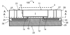
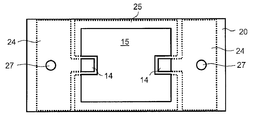
도 1a 및 도 1b는 일 실시 예에 따른 발광 반도체 컴포넌트(100)를 보여준다. 도 1b는 도 1a에 도시된 반도체 컴포넌트(100)를 도 1a에 표시된 절단 평면(A-A)을 따라 절단한 단면도를 보여준다. 도 1b에서 점선은 반도체 칩(1) 바로 아래의 전기 접속 소자(24)들 및 열적 접속 소자(25)의 횡단면들을 표시한다. 1A and 1B show a light emitting
발광 반도체 컴포넌트(100)는 발광 반도체 칩(1)을 포함하고, 상기 발광 반도체 칩은 캐리어 몸체(2)에 의해 지지된다.The light emitting
발광 반도체 칩(1)은 반도체 층 시퀀스를 포함하고, 상기 반도체 층 시퀀스는 상기 반도체 칩의 작동중에 광을 방사하는 적어도 하나의 활성 층을 구비한다. 추가로 발광 반도체 칩(1)은 성장 기판 또는 캐리어 기판 형태의 기판을 포함할 수 있으며, 상기 기판상에는 반도체 층 시퀀스가 배치되어 있다. 명확한 개관을 위해서 반도체 칩(1)의 반도체 층 시퀀스 및 기판은 도 1a에 나타나있지 않다. 도 2a 및 도 2b와 관련하여 발광 반도체 칩(1)을 위한 실시 예들이 나타나 있고, 상기 실시 예들은 아래에서 계속 기술된다.The light emitting
작동중에 생성된 광은 광 방출면(11)을 통해 방사된다. 반도체 칩(1)은 광 방출면(11)에 마주 놓인 후면(12)을 포함한다. 상기 광 방출면(11) 및 상기 후면(12)은 측면(13)들을 통해 서로 연결되어 있다. 작동중에 생성된 광은 광 방출면(11)에 대해 추가적으로 측면들 및/또는 후면(12)의 부분들을 통해 방사될 수 있다. 반도체 칩(1)은 후면(12)에 두 개의 전기 접촉 층(14)을 포함하며, 상기 전기 접촉 층들을 통해 반도체 칩(1) 및 특히 반도체 칩(1)의 반도체 층 시퀀스는 전기적으로 접촉될 수 있다. 추가로 반도체 칩(1)은 열적 접촉 층(15)을 포함하고, 상기 열적 접촉 층은 상기 전기 접촉 층(14)들 및 상기 반도체 칩(1)의 반도체 층 시퀀스에 대해 전기적으로 절연되어 있다. 따라서 상기 열적 접촉 층(15)은 반도체 칩(1) 내에서 전위가 없도록 형성되어 있다. Light generated during operation is emitted through the
도 1b에서 알 수 있는 바와 같이, 열적 접촉 층(15)은 바람직하게 반도체 칩의 후면(12)의 대부분을 형성함으로써, 결과적으로 반도체 칩의 열적 접속이 큰 표면적에서 가능해진다. 특히 상기 열적 접촉 층(15)은 전기 접촉 층(14)들 및 전기 접촉 층(14)들에 대한 열적 접촉 층(15)의 전기적 절연부를 위한 간격에 이르기까지 전기적 반도체 칩의 전체 후면(12)을 형성할 수 있다. As can be seen in FIG. 1B, the
캐리어 몸체(2)는 반도체 칩(1)의 측면(13)들을 형상 구속 방식으로 직접 덮는 성형 몸체(20)를 포함한다. 이 경우, 상기 성형 몸체(20)는 도 1a에 도시된 바와 같이, 반도체 칩(1)의 측면(13)들을 완전히 덮도록 형성될 수 있다. 대안적으로 또한 반도체 칩(1)의 측면(13)들이 성형 몸체(20)에 의해 단지 부분적으로만 덮임으로써, 결과적으로 상기 성형 몸체가 반도체 칩(1)보다 낮은 높이를 갖는 것도 가능하다. 특히 바람직하게 성형 몸체(20)는 반도체 칩(1)의 광 방출면(11)을 덮지 않고, 도 1a에 도시된 바와 같이 광 방출면(11)과 동일 선상에서 종료하는 상부면(21)을 포함한다.The
추가로 성형 몸체(20)의 자체 상부면(21)은 광 방출면(11)을 덮지 않고, 이 광 방출면(11) 위로 돌출할 수 있다. 그럼으로써, 캐리어 몸체(2)의 기계적 안정성이 상승할 수 있다. 그럼으로써, 추가로 광 방출면(11) 위로 리세스가 형성될 수 있고, 상기 리세스 내부에는 예컨대 파장 변환 소자(3)가 배치될 수 있다.The self-
도시된 실시 예에 대안적으로 성형 몸체(20)는 광 방출면(11)을 덮음으로써, 결과적으로 반도체 칩(1)이 캐리어 몸체(2) 내에 포함되고 이 캐리어 몸체에 의해 모든 면이 둘러싸일 수도 있다. 원하는 광학적 특성들, 예컨대 원하는 광 집중 또는 광 분산 특성을 갖기 위해 상기 성형 몸체(20)는 광 방출면(11) 위에서 예컨대 의도대로 형성되거나 특정 재료로 형성될 수 있는데, 예를 들어 렌즈 형태로 형성되거나 충전제를 포함할 수 있다. Alternatively, the molded
성형 몸체(20)는 반도체 칩(1)에 일체로 형성되어 있고, 성형 공정에서 처리될 수 있는 재료, 예를 들어 에폭시드, 실리콘, 실리콘-에폭시드-하이브리드 재료 또는 폴리에스테르를 포함하거나 상기 재료들로 형성되었다. 반도체 칩(1)의 방사 특성에 따라서 성형 몸체(20)는 투과성을 갖도록, 광 흡수 작용하도록, 광 반사 작용하도록 또는 광 산란 작용하도록 형성될 수 있으며, 상응하는 입자 및/또는 충전제를 전술된 재료 내에 포함할 수 있다.The
반도체 칩(1)의 광 방출면(11) 상에 그리고 그에 따라 캐리어 몸체(2) 또는 성형 몸체(20)의 상부면(21) 상에는 파장 변환 소자(3)가 제공될 수 있고, 상기 파장 변환 소자는 발광 반도체 칩(1)에서 생성된 광의 적어도 한 부분을 이 광과 상이한 광으로 변환시킬 수 있다.The
발광 반도체 컴포넌트(100)의 제조를 위해 반도체 칩(1)이 제공된다.A semiconductor chip (1) is provided for manufacturing the light emitting semiconductor component (100).
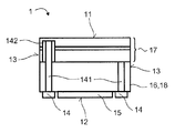
상기 목적을 위해 도 2a 및 도 2b는 발광 반도체 칩(1)을 위한 실시 예들을 보여주고, 상기 발광 반도체 칩은 각각 발광 반도체 컴포넌트(100)를 위해 제공될 수 있으며 각각 하나의 기판(16)을 갖는데, 상기 기판상에는 활성 영역을 갖는 반도체 층 시퀀스(17)가 배치되어 있다.2A and 2B show embodiments for a light emitting
도 2a는 기판(16)이 반도체 층 시퀀스(17)의 제조를 위한 성장 기판으로 형성된 경우의 발광 반도체 칩(1)을 보여준다. 상기 반도체 층 시퀀스(17)의 구조화에 의해서 전기 접촉 층(14)들이 반도체 층 시퀀스(17)의 동일한 측면 상에 배치될 수 있다.2A shows a light emitting
추가로 반도체 칩(1)은 반도체 층 시퀀스(17) 상에 열적 접촉 층(15)을 포함하며, 상기 열적 접촉 층(15)은 패시베이션 층(19)으로 형성된 전기 절연 층(18)에 의해 상기 반도체 층 시퀀스(17)에 대해 전기적으로 절연되어 있다. 상기 패시베이션 층은 바람직하게 이산화규소, 다이아몬드 또는 산화 알루미늄을 포함하고 100㎚보다 크거나 같은 두께를 갖는다.The
이와 달리, 도 2b의 발광 반도체 칩(1)은 캐리어 기판으로서 형성된 세라믹 기판을 기판(16)으로서 포함하고, 상기 세라믹 기판상에는 반도체 층 시퀀스(17)가 성장 기판상에서 성장된 이후에 적용된다. 반도체 층 시퀀스(17)를 등지는 기판(16)의 측면 상에는 전기 접촉 층(14)들이 제공되어 전기 피드스루(141)를 통해 상기 반도체 층 시퀀스(17)와 접촉하고 있다. 도면 부호(142)는 기판(16)을 등지는 반도체 층 시퀀스(17)의 측면을 접촉시키기 위한 피드스루(141)의 전기 절연부를 표시한다.Alternatively, the light emitting
반도체 층 시퀀스(17)를 등지는 기판(16)의 측면 상에는 추가로 열적 접촉 층(15)이 제공되어 있고, 이 경우 기판(16)은 상기 열적 접촉 층(15)을 상기 반도체 층 시퀀스(17)에 대해 전기적으로 절연시키기 위하여 전기 절연 층(18)을 형성한다. A further
발광 반도체 칩(1)이 제공된 후에는 캐리어 몸체(2)가 제조된다. 상기 목적을 위해, 제 1 부분 단계에서 반도체 칩(1)의 측면(13)들이 성형 몸체(20)의 재료에 의해 형상 구속 방식으로 직접 덮인다. 상기 제 1 부분 단계는 성형 공정에서, 도시된 실시 예에서는 특히 이송 성형 공정에서 성형 몸체(20)에 의해 반도체 칩이 변형됨으로써 이루어진다.After the light emitting
캐리어 몸체(2)를 제조하기 위한 추가의 일 방법 단계에서는 반도체 칩의 접촉 층(14, 15)들과 직접 접촉하는 접속 소자(24, 25)들이 형성된다. 상기 목적을 위해, 전기 접속 소자(24)들 및 열적 접속 소자(25)의 일 부분이 갈바닉 공정에 의해서 전기 접촉 층(14)들 및 열적 접촉 층(15) 상에 제공된다. 도 1a로부터 알 수 있는 바와 같이, 전기 접속 소자(24)들은 반도체 칩(1)으로부터 출발하여 부분적으로 성형 몸체(20) 상에도 제공될 수 있다.In a further method step for manufacturing the
후속하여 전기 접속 소자(24)들 및 열적 접속 소자(25)의 이미 제공된 부분을 덮는 전기 절연 재료(26)가 제공된다. 상기 전기 절연 재료(26)는 열적 접속 소자(25)의 이미 제공된 부분을 통해 재차 제거됨으로써, 결과적으로 상기 열적 접속 소자의 부분은 갈바닉 공정의 속행에 의해 계속 보강될 수 있다. 그럼으로써 특히, 열적 접속 소자(24)들을 전기 절연 재료(26) 및 그에 따라 캐리어 몸체(2) 내에 매립하고, 열적 접속 소자(25)를 확장된 폭을 갖도록 제조하는 것이 가능해진다. 그럼으로써, 열적 접속 소자(25)는 전기 접속 소자(24)들보다 두껍고 상기 전기 접속 소자(24)들을 수직 방향에 대해 추가적으로 측면 방향으로도 돌출하도록 형성될 수 있다. 전기 절연 재료(26)는 특히 가령 광 영상화 래커(photoimageable lacquar)와 같은 광 영상화 재료로 형성되는데, 예컨대 BCB를 기본으로 하는 폴리머로 형성된다.There is provided an electrically insulating
전기 접속 소자(24)들 및 열적 접속 소자(25)는 특히 구리 및/또는 니켈을 포함한다. 바람직하게 접속 소자(24, 25)들은 갈바닉 공정에 의해 공정 기술적으로 간단하게 제공되는 구리로 형성된다.The electrical connecting
갈바닉 공정에 의해서는 접속 소자(24, 25)들과 접촉 층(14, 15)들 사이에서 공정 기술적으로 간단한 연결이 가능해지는데, 상기 연결은 약 50㎛ 치수의 작은 구조 폭을 허용한다. 얇은 접속 소자(24, 25)들의 경우에는 예를 들어 열 하중에 의해 야기된 작은 응력이 반도체 칩(1) 상에 도달될 수 있는 반면, 전기 접속 소자(24)들에 비해 현저히 더 두꺼운 열적 접속 소자(25)는 우수한 열 전도성을 가능하게 한다. 열적 접촉 층(15)이 전위가 없도록, 즉 전기적으로 절연되어 반도체 칩(1)의 반도체 층 시퀀스(17) 상에 형성되어 있음으로써, 열적 접속 소자(25)도 마찬가지로 상기 반도체 칩(1)의 반도체 층 시퀀스(17)에 대해 전기적으로 절연되어, 결과적으로 상기 열적 접속 소자(25)의 추가적인 전기적 절연부가 필요하지 않게 된다.The galvanic process allows for a simple and technically simple connection between the
전기 접속 소자(24)들의 외부로부터의 전기적 접촉은 도시된 실시 예와 같이, 성형 몸체(20) 내의 전기 피드스루(27)를 통해 이루어질 수 있다. 상기 전기 피드스루는 소위 바이어의 형태로 형성될 수 있고, 상기 바이어는 예를 들어 별개의 소자로서 발광 반도체 칩(1)과 함께 제공되고 성형 몸체(20)에 의해 변형된다. 추가로 성형 몸체(20) 내에는 개구들이 제공되거나 형성될 수 있고, 상기 개구들은 전기 피드스루를 형성하기 위해 전기 전도성 재료로 적어도 부분적으로 또는 완전히 채워진다. 전기 피드스루(27)에 의해서는 발광 반도체 칩(1) 및 그에 따라 발광 반도체 컴포넌트(100)를 캐리어 몸체(2)의 상부면(21)으로부터 접촉하는 것이 가능하며, 결과적으로 열적 접속 소자(25)는 바람직하게 상기 상부면(21)에 마주 놓인 전체 장착면(22)을 형성하게 된다. Electrical contact from the outside of the
발광 반도체 컴포넌트(100)는 특히 바람직하게 추가의 반도체 컴포넌트들과 연결된 복합체로 제조될 수 있다. 상기 목적을 위해, 다수의 발광 반도체 칩(1)은 공동의 성형 몸체(20)에 의해 변형될 수 있다. 전기 및 열적 접속 소자(24, 25)들 및 경우에 따라서 전기 피드스루(27)가 형성된 이후에 그리고 그에 따라 캐리어 몸체 복합체가 제조된 이후에 상기 컴포넌트 복합체는 개별적인 반도체 컴포넌트(100)로 분리될 수 있다. 상기 분리 공정을 통해 캐리어 몸체(2)의 측면들이 생성되고, 상기 측면들은 예를 들어 소잉 홈(sawing groove) 또는 연삭흔(grinding mark)의 형태로 분리 공정에서 비롯된 재료 제거 흔적을 가질 수 있다.The light emitting
도 3은 추가의 일 실시 예에 따른 발광 반도체 컴포넌트(200)를 보여주며, 상기 발광 반도체 컴포넌트는 발광 반도체 컴포넌트(100)와 달리 장착면(22)으로부터 전기적 접촉을 가능하게 한다. 상기 목적을 위해, 열적 접속 소자(25)는 개구들을 포함하고, 상기 개구들 내에는 전기 피드스루(27)가 배치되어 전기 절연 재료(26)에 의해 열적 접속 소자(25)에 대해 절연되어 있다.FIG. 3 illustrates a light emitting
추가로 상부면(21)뿐만 아니라 하부면 혹은 장착면(22) 상에 피드스루(21) 형태로 전기적 접속 가능성들을 제공하는 것도 가능하다.It is further possible to provide electrical connection possibilities in the form of
전기 접속 소자(24)들 및 열적 접속 소자(25)를 제공하기 위한 갈바닉 공정을 통해 그리고 성형 몸체(20) 및/또는 열적 접속 소자(25) 내에서 전기 피드스루(27)의 배치를 통해 장착면(22)은 열적 및 전기 접속 가능성들과 관련하여 임의로 설계될 수 있다.Through a galvanic process to provide
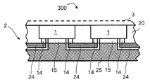
도 4는 발광 반도체 컴포넌트(300)의 추가의 일 실시 예의 부분 확대 단면도를 보여주고, 상기 발광 반도체 컴포넌트는 기존의 실시 예들과 달리, 공동의 성형 몸체(20)에 의해 변형된 다수의 반도체 칩(1)을 포함한다.Figure 4 shows a partially enlarged cross-sectional view of a further embodiment of a light emitting
반도체 칩(1)들은 전기 접속 소자(24)들을 통해 캐리어 몸체(2) 내에서 서로 접속되어 있다. 추가로 발광 반도체 컴포넌트(300)는 열적 접속 소자(25)를 포함하고, 상기 열적 접속 소자에는 반도체 칩(1)의 열적 접촉 층(15)들이 직접적으로 인접함으로써, 결과적으로 상기 열적 접속 소자(25)는 반도체 칩(1)에서 작동중에 생성된 열을 배출시킬 수 있는 연결된 열적 접속 소자로서 형성될 수 있다.The semiconductor chips 1 are connected to each other in the
도면들에 기술된 실시 예들 및 특징들은 서로 조합될 수도 있다. 실시 예들에 나타나 있는 특징들에 대해 추가적으로 또는 대안적으로 발광 반도체 컴포넌트(100, 200, 300)는 전반적인 부분의 설명 내용에 따른 추가의 특징들도 가질 수 있다.The embodiments and features described in the drawings may be combined with one another. In addition to or in addition to the features shown in the embodiments, the light emitting
본 발명은 실시 예들을 참조한 설명 내용에만 한정되지 않는다. 오히려 본 발명은 각각의 새로운 특징 및 특징들의 각각의 조합을 포함하며, 이는 비록 상기 특징 또는 상기 조합 자체가 특허청구범위 또는 실시 예들에 명시적으로 기재되어 있지 않더라도, 특히 특허청구범위 내 특징들의 각각의 조합을 포함한다. The present invention is not limited to the description with reference to the embodiments. Rather, the present invention includes each combination of each new feature or feature, and even though the feature or combination itself is not explicitly recited in the claims or embodiments, . ≪ / RTI >
Claims (15)
반도체 층 시퀀스(17), 광 방출면(11), 상기 광 방출면(11)에 마주 놓인 후면(12) 및 상기 광 방출면(11)과 상기 후면(12)을 연결하는 측면(13)들을 갖는 적어도 하나의 발광 반도체 칩(1) 및
캐리어 몸체(2)를 포함하고, 상기 캐리어 몸체는 반도체 칩(1)의 측면(13)들을 형상 구속(form-locked) 방식으로 직접 덮는 성형 몸체(20)를 구비하며,
이때 상기 반도체 칩(1)의 후면(12)에는 두 개의 전기 접촉 층(14) 및 하나의 열적 접촉 층(15)이 형성되어 있고,
상기 열적 접촉 층(15)은 상기 전기 접촉 층(14)들 및 상기 반도체 층 시퀀스(17)에 대해 전기적으로 절연되어 있으며,
상기 캐리어 몸체(2)는 반도체 칩(1)의 후면(12)에서 반도체 칩(1)의 전기 접촉 층(14)들과 직접 접촉하는 전기 접속 소자(24)들 및 반도체 칩(1)의 열적 접촉 층(15)과 직접 접촉하는 열적 접속 소자(25)를 포함하며,
상기 열적 접속 소자(25)는 적어도 부분적으로 반도체 칩(1)을 등지는 반도체 컴포넌트(100, 200, 300)의 장착면(22)을 형성하는,
발광 반도체 컴포넌트. A light emitting semiconductor component (100, 200, 300)
A semiconductor layer sequence 17, a light emitting surface 11, a rear surface 12 opposed to the light emitting surface 11, and side surfaces 13 connecting the light emitting surface 11 and the rear surface 12 At least one light emitting semiconductor chip (1) and
And a carrier body 2 having a molding body 20 for directly covering the side surfaces 13 of the semiconductor chip 1 in a form-locked manner,
At this time, two electrical contact layers 14 and one thermal contact layer 15 are formed on the rear surface 12 of the semiconductor chip 1,
The thermal contact layer 15 is electrically isolated from the electrical contact layers 14 and the semiconductor layer sequence 17,
The carrier body 2 is electrically connected to the electrical contact elements 24 in direct contact with the electrical contact layers 14 of the semiconductor chip 1 at the rear surface 12 of the semiconductor chip 1, And a thermal contact element (25) in direct contact with the contact layer (15)
The thermal connection element 25 is formed at least partially on the mounting surface 22 of the semiconductor component 100, 200, 300,
Light emitting semiconductor component.
상기 성형 몸체(20)는 상기 광 방출면(11)을 덮지 않는,
발광 반도체 컴포넌트.The method according to claim 1,
The molding body (20) does not cover the light emitting surface (11)
Light emitting semiconductor component.
상기 성형 몸체(20)는 상기 광 방출면(11)과 동일 선상에서 종료하는,
발광 반도체 컴포넌트.3. The method according to claim 1 or 2,
The molding body (20) has a light emitting surface (11)
Light emitting semiconductor component.
상기 광 방출면(11) 상에 파장 변환 소자(3)가 배치되어 있는,
발광 반도체 컴포넌트.4. The method according to any one of claims 1 to 3,
Wherein the wavelength conversion element (3) is arranged on the light emitting surface (11)
Light emitting semiconductor component.
상기 캐리어 몸체(2)는 전기 접속 소자(24)들과 열적 접속 소자(25) 사이에 전기 절연 재료(26)를 포함하는,
발광 반도체 컴포넌트.5. The method according to any one of claims 1 to 4,
The carrier body 2 comprises an electrically insulating material 26 between the electrical connecting elements 24 and the thermally connecting element 25. [
Light emitting semiconductor component.
상기 전기 접속 소자(24)들은 상기 캐리어 몸체(2)의 내부에 배치되어 있는,
발광 반도체 컴포넌트.6. The method according to any one of claims 1 to 5,
The electrical connection elements (24) are arranged inside the carrier body (2)
Light emitting semiconductor component.
상기 전기 접속 소자(24)들은 부분적으로 상기 성형 몸체(20) 상에 제공되어 있는,
발광 반도체 컴포넌트.7. The method according to any one of claims 1 to 6,
The electrical connection elements (24) are partly provided on the molding body (20)
Light emitting semiconductor component.
상기 열적 접속 소자(25)는 상기 전기 접속 소자(24)들을 측면 방향으로 돌출하는,
발광 반도체 컴포넌트. 8. The method according to any one of claims 1 to 7,
The thermal connection element (25) includes a plurality of electrical connection elements (24) projecting laterally,
Light emitting semiconductor component.
상기 전기 접속 소자(24)들 및 상기 열적 접속 소자(25)는 갈바닉 방식으로 반도체 칩(1) 상에 제공되는,
발광 반도체 컴포넌트.9. The method according to any one of claims 1 to 8,
The electrical connection elements 24 and the thermal connection element 25 are provided on the semiconductor chip 1 in a galvanic manner,
Light emitting semiconductor component.
상기 성형 몸체(20)는 적어도 하나의 전기 피드스루(electric feedthrough)를 갖고, 상기 전기 피드스루는 하나의 전기 접속 소자(24)와 전기적으로 연결되어 있는,
발광 반도체 컴포넌트.10. The method according to any one of claims 1 to 9,
Wherein the forming body (20) has at least one electric feedthrough, wherein the electrical feedthrough is electrically connected to one electrical connection element (24)
Light emitting semiconductor component.
상기 열적 접속 소자(25)는 반도체 컴포넌트(100, 200, 300)의 전체 장착면(22)을 형성하는,
발광 반도체 컴포넌트.11. The method of claim 10,
The thermal contact element 25 is formed of a material that forms the entire mounting surface 22 of the semiconductor component 100, 200,
Light emitting semiconductor component.
상기 반도체 칩(1)은 반도체 칩 시퀀스(17)와 열적 접촉 층(15) 사이에 전기 절연 층(18)을 포함하는,
발광 반도체 컴포넌트.12. The method according to any one of claims 1 to 11,
The semiconductor chip 1 includes an electrically insulating layer 18 between the semiconductor chip sequence 17 and the thermal contact layer 15. The semiconductor chip 1 includes an electrically insulating layer 18,
Light emitting semiconductor component.
상기 열적 접촉 층(15)은 반도체 칩(1)의 후면(12)에서 상기 전기 접촉 층(14)들보다 더 큰 표면적을 차지하는,
발광 반도체 컴포넌트.13. The method according to any one of claims 1 to 12,
The thermal contact layer 15 occupies a larger surface area than the electrical contact layers 14 at the back surface 12 of the semiconductor chip 1. [
Light emitting semiconductor component.
상기 성형 몸체(20) 내에 다수의 발광 반도체 칩(1)이 측면으로 나란히 배치되어 있고, 상기 캐리어 몸체(2)는 연결된 열적 접속 소자(25)를 포함하며, 상기 열적 접속 소자와 반도체 칩(1)들의 열적 접촉 층(15)들은 직접 접촉하는,
발광 반도체 컴포넌트.14. The method according to any one of claims 1 to 13,
A plurality of light emitting semiconductor chips 1 are arranged side by side in the molding body 20 and the carrier body 2 includes a connected thermal connecting element 25 and the thermal connecting element and the semiconductor chip 1 Are in direct contact with each other,
Light emitting semiconductor component.
A) 반도체 층 시퀀스(17), 광 방출면(11), 상기 광 방출면(11)에 마주 놓인 후면(12) 및 상기 광 방출면(11)과 상기 후면(12)을 연결하는 측면(13)들을 갖는 발광 반도체 칩(1)을 제공하는 단계로서, 상기 반도체 칩(1)의 후면(12)에는 두 개의 전기 접촉 층(14) 및 하나의 열적 접촉 층(15)이 배치되어 있고, 상기 열적 접촉 층(15)은 상기 전기 접촉 층(14)들과 상기 반도체 층 시퀀스(17)에 대해 전기적으로 절연되어 있는 단계;
B) 상기 반도체 칩(1)을 위해 캐리어 몸체(2)를 다음의 부분 단계들로 형성하는 단계:
B1) 상기 반도체 칩(1)의 측면(13)들을 형상 구속 방식으로 직접 덮는 성형 몸체(20)에 의해 상기 반도체 칩(1)을 변형시키는 단계;
B2) 갈바닉 공정에 의해 반도체 칩(1)의 전기 접촉 층(14)들과 직접 접촉하는 전기 접속 소자(24)들 및 반도체 칩(1)의 열적 접촉 층(15)과 직접 접촉하는 열적 접속 소자(25)를 형성하는 단계로서, 상기 열적 접속 소자(25)는 반도체 칩(1)을 등지는 반도체 컴포넌트(100, 200, 300)의 장착면(22)을 형성하는 두께로 제공되는 단계를 포함하는,
발광 반도체 컴포넌트의 제조 방법.A method of manufacturing a light emitting semiconductor component (100, 200, 300) according to any one of claims 1 to 14,
A) a semiconductor layer sequence 17, a light emitting surface 11, a rear surface 12 opposed to the light emitting surface 11, and a side surface 13 connecting the light emitting surface 11 and the rear surface 12 , Wherein two electrical contact layers (14) and one thermal contact layer (15) are arranged on the rear surface (12) of the semiconductor chip (1) Wherein the thermal contact layer (15) is electrically isolated from the electrical contact layer (14) and the semiconductor layer sequence (17);
B) forming the carrier body (2) for the semiconductor chip (1) with the following partial steps:
B1) deforming the semiconductor chip (1) by a molding body (20) directly covering the side surfaces (13) of the semiconductor chip (1) in a shape constraining manner;
B2) electrically connecting elements (24) in direct contact with the electrical contact layers (14) of the semiconductor chip (1) by a galvanic process and a thermal contact element (14) in direct contact with the thermal contact layer (15) Wherein the thermal connection element 25 is provided with a thickness that forms a mounting surface 22 of the semiconductor component 100, 200, 300, such as the semiconductor chip 1, doing,
A method of manufacturing a light emitting semiconductor component.
Applications Claiming Priority (3)
| Application Number | Priority Date | Filing Date | Title |
|---|---|---|---|
| DE102012102847A DE102012102847A1 (en) | 2012-04-02 | 2012-04-02 | A light-emitting semiconductor component and method for producing a light-emitting semiconductor component |
| DE102012102847.8 | 2012-04-02 | ||
| PCT/EP2013/054050 WO2013149772A1 (en) | 2012-04-02 | 2013-02-28 | Light-emitting semiconductor component and method for producing a light-emitting semiconductor component |
Publications (1)
| Publication Number | Publication Date |
|---|---|
| KR20150002627A true KR20150002627A (en) | 2015-01-07 |
Family
ID=47845967
Family Applications (1)
| Application Number | Title | Priority Date | Filing Date |
|---|---|---|---|
| KR1020147027027A Withdrawn KR20150002627A (en) | 2012-04-02 | 2013-02-28 | Light-emitting semiconductor component and method for producing a light-emitting semiconductor component |
Country Status (6)
| Country | Link |
|---|---|
| US (1) | US9954150B2 (en) |
| JP (1) | JP2015513226A (en) |
| KR (1) | KR20150002627A (en) |
| CN (1) | CN104221173B (en) |
| DE (2) | DE102012102847A1 (en) |
| WO (1) | WO2013149772A1 (en) |
Families Citing this family (25)
| Publication number | Priority date | Publication date | Assignee | Title |
|---|---|---|---|---|
| DE102012111247A1 (en) | 2012-11-21 | 2014-05-22 | Osram Opto Semiconductors Gmbh | Optoelectronic semiconductor device |
| DE102013210668A1 (en) * | 2013-06-07 | 2014-12-11 | Würth Elektronik GmbH & Co. KG | Method for producing an optical module |
| DE102014108295A1 (en) | 2014-06-12 | 2015-12-17 | Osram Opto Semiconductors Gmbh | Light-emitting semiconductor device |
| DE102014109779A1 (en) * | 2014-06-13 | 2015-12-17 | Osram Opto Semiconductors Gmbh | Method for producing an assembly with a component |
| JP6414454B2 (en) * | 2014-10-24 | 2018-10-31 | 日亜化学工業株式会社 | Light emitting device and manufacturing method thereof |
| CN110690249B (en) | 2015-02-13 | 2024-01-19 | 首尔伟傲世有限公司 | Light emitting element |
| KR102424364B1 (en) * | 2015-05-27 | 2022-07-25 | 서울바이오시스 주식회사 | Light emitting diode |
| WO2016157518A1 (en) * | 2015-04-03 | 2016-10-06 | 創光科学株式会社 | Nitride-semiconductor ultraviolet-light emitting device and nitride-semiconductor ultraviolet-light emitting apparatus |
| DE102015113310B4 (en) * | 2015-08-12 | 2022-08-04 | OSRAM Opto Semiconductors Gesellschaft mit beschränkter Haftung | semiconductor chip |
| DE102015115900A1 (en) * | 2015-09-21 | 2017-03-23 | Osram Opto Semiconductors Gmbh | Semiconductor device and method for manufacturing a semiconductor device |
| US10118547B2 (en) * | 2015-11-13 | 2018-11-06 | The Boeing Company | Embedded lighting features for lighting panels |
| DE102015120642A1 (en) | 2015-11-27 | 2017-06-01 | Osram Opto Semiconductors Gmbh | Device with at least one optoelectronic semiconductor component |
| DE102016100320A1 (en) | 2016-01-11 | 2017-07-13 | Osram Opto Semiconductors Gmbh | Optoelectronic component, optoelectronic module and method for producing an optoelectronic component |
| JP6447557B2 (en) * | 2016-03-24 | 2019-01-09 | 日亜化学工業株式会社 | Method for manufacturing light emitting device |
| CN107482099B (en) * | 2016-06-08 | 2019-09-10 | 光宝光电(常州)有限公司 | Light emitting diode packaging structure |
| DE102016121510A1 (en) | 2016-11-10 | 2018-05-17 | Osram Opto Semiconductors Gmbh | Leadframe, optoelectronic component with a leadframe and method for producing an optoelectronic component |
| DE102017123898A1 (en) * | 2017-10-13 | 2019-04-18 | Osram Opto Semiconductors Gmbh | Semiconductor device and method for manufacturing semiconductor devices |
| TWI642335B (en) * | 2017-12-11 | 2018-11-21 | 欣興電子股份有限公司 | Circuit board and manufacturing method thereof |
| DE102018119538A1 (en) | 2018-08-10 | 2020-02-13 | Osram Opto Semiconductors Gmbh | OPTOELECTRONIC SEMICONDUCTOR COMPONENT AND PRODUCTION METHOD FOR OPTOELECTRONIC SEMICONDUCTOR COMPONENTS |
| DE102019104010B4 (en) | 2019-02-18 | 2025-08-28 | Infineon Technologies Austria Ag | ELECTRONIC MODULE WITH IMPROVED HEAT DISSIPATION AND ITS MANUFACTURE |
| DE102019120717A1 (en) * | 2019-07-31 | 2021-02-04 | OSRAM Opto Semiconductors Gesellschaft mit beschränkter Haftung | METHOD FOR MANUFACTURING AN ELECTRONIC COMPONENT AND ELECTRONIC COMPONENT |
| CN113054042B (en) * | 2021-03-15 | 2022-07-08 | 河南城建学院 | Optoelectronic semiconductor component with substrate structure |
| US20250160053A1 (en) * | 2022-02-17 | 2025-05-15 | Ams-Osram International Gmbh | Production method, optoelectronic semiconductor component, and carrier |
| CN118974956A (en) * | 2022-03-30 | 2024-11-15 | 亮锐有限责任公司 | Semiconductor structure and method of manufacturing a semiconductor structure |
| US20240162393A1 (en) * | 2022-11-11 | 2024-05-16 | Seoul Semiconductor Co., Ltd. | Light source module |
Family Cites Families (18)
| Publication number | Priority date | Publication date | Assignee | Title |
|---|---|---|---|---|
| JP4432275B2 (en) | 2000-07-13 | 2010-03-17 | パナソニック電工株式会社 | Light source device |
| US6507049B1 (en) * | 2000-09-01 | 2003-01-14 | General Electric Company | Encapsulants for solid state devices |
| ATE425556T1 (en) * | 2001-04-12 | 2009-03-15 | Matsushita Electric Works Ltd | LIGHT SOURCE COMPONENT WITH LED AND METHOD FOR PRODUCING IT |
| WO2002089221A1 (en) | 2001-04-23 | 2002-11-07 | Matsushita Electric Works, Ltd. | Light emitting device comprising led chip |
| US6880100B2 (en) | 2001-07-18 | 2005-04-12 | Smartmatic Corp. | Peer-to-peer fault detection |
| JP4122784B2 (en) | 2001-09-19 | 2008-07-23 | 松下電工株式会社 | Light emitting device |
| US6498355B1 (en) | 2001-10-09 | 2002-12-24 | Lumileds Lighting, U.S., Llc | High flux LED array |
| DE10214210B4 (en) | 2002-03-28 | 2011-02-10 | Osram Opto Semiconductors Gmbh | Lumineszenzdiodenchip for flip-chip mounting on a soldered carrier and method for its preparation |
| KR100867970B1 (en) | 2004-10-04 | 2008-11-11 | 가부시끼가이샤 도시바 | Light emitting device, lighting equipment, or liquid crystal display device using such light emitting device |
| US7355276B1 (en) | 2005-03-11 | 2008-04-08 | Maxtor Corporation | Thermally-enhanced circuit assembly |
| FI20095557A0 (en) * | 2009-05-19 | 2009-05-19 | Imbera Electronics Oy | Manufacturing process and electronics module with new wiring possibilities |
| DE102009036621B4 (en) | 2009-08-07 | 2023-12-21 | OSRAM Opto Semiconductors Gesellschaft mit beschränkter Haftung | Optoelectronic semiconductor component |
| US20110049545A1 (en) * | 2009-09-02 | 2011-03-03 | Koninklijke Philips Electronics N.V. | Led package with phosphor plate and reflective substrate |
| KR101601622B1 (en) | 2009-10-13 | 2016-03-09 | 삼성전자주식회사 | Light emitting diode device, light emitting device and method of manufacturing light emitting diode device |
| US8248803B2 (en) * | 2010-03-31 | 2012-08-21 | Hong Kong Applied Science and Technology Research Institute Company Limited | Semiconductor package and method of manufacturing the same |
| CN101984511B (en) * | 2010-11-10 | 2016-06-01 | 秦彪 | LED chip and LED wafer and manufacturing method of chip |
| US8299488B2 (en) * | 2010-12-16 | 2012-10-30 | King Dragon International Inc. | LED chip |
| KR20120091839A (en) * | 2011-02-10 | 2012-08-20 | 삼성전자주식회사 | Flip chip light emitting device package and manufaturing method thereof |
-
2012
- 2012-04-02 DE DE102012102847A patent/DE102012102847A1/en not_active Withdrawn
-
2013
- 2013-02-28 KR KR1020147027027A patent/KR20150002627A/en not_active Withdrawn
- 2013-02-28 US US14/382,578 patent/US9954150B2/en not_active Expired - Fee Related
- 2013-02-28 CN CN201380018936.0A patent/CN104221173B/en not_active Expired - Fee Related
- 2013-02-28 WO PCT/EP2013/054050 patent/WO2013149772A1/en not_active Ceased
- 2013-02-28 JP JP2015502171A patent/JP2015513226A/en active Pending
- 2013-02-28 DE DE112013001861.6T patent/DE112013001861A5/en not_active Ceased
Also Published As
| Publication number | Publication date |
|---|---|
| US9954150B2 (en) | 2018-04-24 |
| WO2013149772A1 (en) | 2013-10-10 |
| US20150041845A1 (en) | 2015-02-12 |
| DE102012102847A1 (en) | 2013-10-02 |
| JP2015513226A (en) | 2015-04-30 |
| CN104221173B (en) | 2018-01-05 |
| DE112013001861A5 (en) | 2014-12-18 |
| CN104221173A (en) | 2014-12-17 |
Similar Documents
| Publication | Publication Date | Title |
|---|---|---|
| KR20150002627A (en) | Light-emitting semiconductor component and method for producing a light-emitting semiconductor component | |
| KR101781061B1 (en) | Optoelectronic component and method for producing same | |
| JP6530442B2 (en) | Semiconductor light emitting diode having reflective structure and method of manufacturing the same | |
| US8309979B2 (en) | Electrically isolated vertical light emitting diode structure | |
| CN101681964B (en) | Method for manufacturing an optoelectronic device and optoelectronic device | |
| KR101891257B1 (en) | Light Emitting Device and Manufacturing Method thereof | |
| EP2519961B1 (en) | Thin-film led with p and n contacts electrically isolated from the substrate | |
| CN104737307B (en) | Method for manufacturing multiple opto-electronic semiconductor components | |
| US7491981B2 (en) | Light-emitting device and glass seal member therefor | |
| JP6621797B2 (en) | Method for manufacturing a plurality of optoelectronic components | |
| KR102074027B1 (en) | Method for producing an optoelectronic semiconductor device, and optoelectronic semiconductor device | |
| US9548433B2 (en) | Light-emitting diode chip | |
| US9601663B2 (en) | Light-emitting diode chip | |
| US9653670B2 (en) | Method for producing an optoelectronic semiconductor component, and optoelectronic semiconductor component | |
| US10854793B2 (en) | Method for producing an optoelectronic component and optoelectronic component | |
| US8598612B2 (en) | Light emitting diode thermally enhanced cavity package and method of manufacture | |
| CN102414849A (en) | Light emitting diode and method for manufacturing light emitting diode | |
| CN114365296B (en) | Method for producing a radiation-emitting semiconductor chip, radiation-emitting semiconductor chip and radiation-emitting component | |
| US20240421278A1 (en) | Semiconductor light emitting device and method for manufacturing the same | |
| US20210184092A1 (en) | Optoelectronic component, optoelectronic module, and method of producing an optoelectronic component | |
| KR101526087B1 (en) | Housing and method for producing a housing for an optoelectronic component | |
| US20190140145A1 (en) | Light-Emitting Device and Method for Manufacturing a Light-Emitting Device | |
| CN110998873A (en) | Semiconductor chip with transparent current spreading layer | |
| US20170345981A1 (en) | Light-emitting device | |
| KR20180065619A (en) | Compound semiconductor opticla device |
Legal Events
| Date | Code | Title | Description |
|---|---|---|---|
| PA0105 | International application |
Patent event date: 20140925 Patent event code: PA01051R01D Comment text: International Patent Application |
|
| PG1501 | Laying open of application | ||
| PC1203 | Withdrawal of no request for examination | ||
| WITN | Application deemed withdrawn, e.g. because no request for examination was filed or no examination fee was paid |