KR101891257B1 - Light Emitting Device and Manufacturing Method thereof - Google Patents
Light Emitting Device and Manufacturing Method thereof Download PDFInfo
- Publication number
- KR101891257B1 KR101891257B1 KR1020120033978A KR20120033978A KR101891257B1 KR 101891257 B1 KR101891257 B1 KR 101891257B1 KR 1020120033978 A KR1020120033978 A KR 1020120033978A KR 20120033978 A KR20120033978 A KR 20120033978A KR 101891257 B1 KR101891257 B1 KR 101891257B1
- Authority
- KR
- South Korea
- Prior art keywords
- light emitting
- substrate
- electrode
- emitting structure
- semiconductor layer
- Prior art date
- Legal status (The legal status is an assumption and is not a legal conclusion. Google has not performed a legal analysis and makes no representation as to the accuracy of the status listed.)
- Expired - Fee Related
Links
Images


Classifications
-
- H—ELECTRICITY
- H10—SEMICONDUCTOR DEVICES; ELECTRIC SOLID-STATE DEVICES NOT OTHERWISE PROVIDED FOR
- H10H—INORGANIC LIGHT-EMITTING SEMICONDUCTOR DEVICES HAVING POTENTIAL BARRIERS
- H10H20/00—Individual inorganic light-emitting semiconductor devices having potential barriers, e.g. light-emitting diodes [LED]
- H10H20/80—Constructional details
- H10H20/83—Electrodes
-
- H—ELECTRICITY
- H10—SEMICONDUCTOR DEVICES; ELECTRIC SOLID-STATE DEVICES NOT OTHERWISE PROVIDED FOR
- H10H—INORGANIC LIGHT-EMITTING SEMICONDUCTOR DEVICES HAVING POTENTIAL BARRIERS
- H10H20/00—Individual inorganic light-emitting semiconductor devices having potential barriers, e.g. light-emitting diodes [LED]
- H10H20/01—Manufacture or treatment
-
- H—ELECTRICITY
- H10—SEMICONDUCTOR DEVICES; ELECTRIC SOLID-STATE DEVICES NOT OTHERWISE PROVIDED FOR
- H10H—INORGANIC LIGHT-EMITTING SEMICONDUCTOR DEVICES HAVING POTENTIAL BARRIERS
- H10H20/00—Individual inorganic light-emitting semiconductor devices having potential barriers, e.g. light-emitting diodes [LED]
- H10H20/80—Constructional details
- H10H20/84—Coatings, e.g. passivation layers or antireflective coatings
-
- H—ELECTRICITY
- H10—SEMICONDUCTOR DEVICES; ELECTRIC SOLID-STATE DEVICES NOT OTHERWISE PROVIDED FOR
- H10H—INORGANIC LIGHT-EMITTING SEMICONDUCTOR DEVICES HAVING POTENTIAL BARRIERS
- H10H20/00—Individual inorganic light-emitting semiconductor devices having potential barriers, e.g. light-emitting diodes [LED]
- H10H20/80—Constructional details
- H10H20/85—Packages
- H10H20/857—Interconnections, e.g. lead-frames, bond wires or solder balls
-
- H—ELECTRICITY
- H10—SEMICONDUCTOR DEVICES; ELECTRIC SOLID-STATE DEVICES NOT OTHERWISE PROVIDED FOR
- H10H—INORGANIC LIGHT-EMITTING SEMICONDUCTOR DEVICES HAVING POTENTIAL BARRIERS
- H10H20/00—Individual inorganic light-emitting semiconductor devices having potential barriers, e.g. light-emitting diodes [LED]
- H10H20/01—Manufacture or treatment
- H10H20/032—Manufacture or treatment of electrodes
-
- H—ELECTRICITY
- H10—SEMICONDUCTOR DEVICES; ELECTRIC SOLID-STATE DEVICES NOT OTHERWISE PROVIDED FOR
- H10H—INORGANIC LIGHT-EMITTING SEMICONDUCTOR DEVICES HAVING POTENTIAL BARRIERS
- H10H20/00—Individual inorganic light-emitting semiconductor devices having potential barriers, e.g. light-emitting diodes [LED]
- H10H20/01—Manufacture or treatment
- H10H20/034—Manufacture or treatment of coatings
-
- H—ELECTRICITY
- H10—SEMICONDUCTOR DEVICES; ELECTRIC SOLID-STATE DEVICES NOT OTHERWISE PROVIDED FOR
- H10H—INORGANIC LIGHT-EMITTING SEMICONDUCTOR DEVICES HAVING POTENTIAL BARRIERS
- H10H20/00—Individual inorganic light-emitting semiconductor devices having potential barriers, e.g. light-emitting diodes [LED]
- H10H20/01—Manufacture or treatment
- H10H20/036—Manufacture or treatment of packages
-
- H—ELECTRICITY
- H10—SEMICONDUCTOR DEVICES; ELECTRIC SOLID-STATE DEVICES NOT OTHERWISE PROVIDED FOR
- H10H—INORGANIC LIGHT-EMITTING SEMICONDUCTOR DEVICES HAVING POTENTIAL BARRIERS
- H10H20/00—Individual inorganic light-emitting semiconductor devices having potential barriers, e.g. light-emitting diodes [LED]
- H10H20/80—Constructional details
- H10H20/83—Electrodes
- H10H20/831—Electrodes characterised by their shape
- H10H20/8312—Electrodes characterised by their shape extending at least partially through the bodies
-
- H—ELECTRICITY
- H10—SEMICONDUCTOR DEVICES; ELECTRIC SOLID-STATE DEVICES NOT OTHERWISE PROVIDED FOR
- H10H—INORGANIC LIGHT-EMITTING SEMICONDUCTOR DEVICES HAVING POTENTIAL BARRIERS
- H10H20/00—Individual inorganic light-emitting semiconductor devices having potential barriers, e.g. light-emitting diodes [LED]
- H10H20/80—Constructional details
- H10H20/83—Electrodes
- H10H20/831—Electrodes characterised by their shape
- H10H20/8314—Electrodes characterised by their shape extending at least partially onto an outer side surface of the bodies
-
- H—ELECTRICITY
- H10—SEMICONDUCTOR DEVICES; ELECTRIC SOLID-STATE DEVICES NOT OTHERWISE PROVIDED FOR
- H10W—GENERIC PACKAGES, INTERCONNECTIONS, CONNECTORS OR OTHER CONSTRUCTIONAL DETAILS OF DEVICES COVERED BY CLASS H10
- H10W70/00—Package substrates; Interposers; Redistribution layers [RDL]
- H10W70/60—Insulating or insulated package substrates; Interposers; Redistribution layers
Landscapes
- Led Devices (AREA)
- Led Device Packages (AREA)
Abstract
본 발명의 일 측면에 따른 반도체 발광장치는,
적어도 일면에 형성된 제1 및 제2 전극패턴을 구비하는 기판과, 상기 기판의 일면 상에 배치되며, 제1 도전형 반도체층, 활성층 및 제2 도전형 반도체층을 포함하는 발광구조물과, 상기 제1 도전형 반도체층과 전기적으로 연결되도록 형성되는 제1 전극구조와, 상기 제2 도전형 반도체층과 전기적으로 연결되며 상기 기판과 상기 발광구조물 사이에 형성되어 상기 발광구조물의 외측으로 연장되는 제2 전극구조와, 상기 기판 및 제2 전극구조 사이에 개재되어 상기 기판과 상기 제2 전극구조를 분리하는 절연층와, 상기 제1 전극구조와 상기 제1 전극패턴을 연결하는 제1 연결부와, 상기 발광구조물의 외측으로 연장된 제2 전극구조와 상기 제2 전극패턴을 연결하는 제2 연결부를 포함한다.A semiconductor light emitting device according to an aspect of the present invention includes:
A light emitting structure including a first conductivity type semiconductor layer, an active layer, and a second conductivity type semiconductor layer disposed on one surface of the substrate, the first and second electrode patterns being formed on at least one side of the substrate, A first electrode structure formed to be electrically connected to the first conductivity type semiconductor layer and a second electrode structure formed between the substrate and the light emitting structure and electrically connected to the second conductivity type semiconductor layer, An insulating layer interposed between the substrate and the second electrode structure and separating the substrate from the second electrode structure; a first connection part connecting the first electrode structure and the first electrode pattern; And a second connection portion connecting the second electrode pattern and the second electrode structure extending outside the structure.
Description
본 발명은 반도체 발광장치 및 그 제조방법에 관한 것이다.The present invention relates to a semiconductor light emitting device and a method of manufacturing the same.
일반적으로, 질화물 반도체는 풀컬러 디스플레이, 이미지 스캐너, 각종 신호시스템 및 광 통신기기에 광원으로 제공되는 녹색 또는 청색 발광 다이오드(light emitting diode: LED) 또는 레이저 다이오드(laser diode: LD)에 널리 사용되어 왔다. 이러한 질화물 반도체 발광소자는 전자와 정공의 재결합원리를 이용하는 청색 및 녹색을 포함하는 다양한 광을 방출하는 활성층을 갖는 발광소자로서 제공될 수 있다.
In general, nitride semiconductors are widely used in green or blue light emitting diodes (LED) or laser diodes (LD), which are provided as light sources for full color displays, image scanners, various signal systems and optical communication devices come. Such a nitride semiconductor light emitting device can be provided as a light emitting device having an active layer that emits various light including blue and green using the principle of recombination of electrons and holes.
이러한 질화물 발광소자가 개발된 후에, 많은 기술적 발전이 이루어져 그 활용 범위가 확대되어 일반 조명 및 전장용 광원으로 많은 연구가 되고 있다. 특히, 종래에는 질화물 발광소자는 주로 저 전류/저 출력의 모바일 제품에 적용되는 부품으로 사용되었으며, 최근에는 점차 그 활용범위가 고 전류/고 출력 분야로 확대됨에 따라, 반도체 발광소자의 발광 효율과 품질을 개선하기 위한 연구가 활발하게 이루어지고 있다. 특히, 발광소자의 광 출력과 신뢰성을 개선하기 위해 다양한 전극 구조를 갖는 발광소자가 개발되고 있다.
After the development of such a nitride light emitting device, a lot of technical developments have been made, and the application range of the nitride optical device has been expanded, and many studies have been made as a light source for general illumination and electric field. Particularly, in the past, a nitride light emitting device has mainly been used as a component applied to a mobile product having a low current / low output. In recent years, since its application range has expanded to a high current / high output field, Researches for improving quality have been actively carried out. In particular, a light emitting device having various electrode structures has been developed to improve light output and reliability of the light emitting device.
본 발명의 목적 중 하나는, 신뢰성이 개선된 반도체 발광장치를 제공하는 것이다.One of the objects of the present invention is to provide a semiconductor light emitting device with improved reliability.
본 발명의 목적 중 다른 하나는, 발광구조물과 기판 사이의 안정적이고 견고한 결합이 가능하게 하는 반도체 발광장치 제조방법을 제공하는 것이다.Another object of the present invention is to provide a method of manufacturing a semiconductor light emitting device that enables stable and rigid bonding between a light emitting structure and a substrate.
본 발명의 일 측면은,According to an aspect of the present invention,
적어도 일면에 형성된 제1 및 제2 전극패턴을 구비하는 기판과, 상기 기판의 일면 상에 배치되며, 제1 도전형 반도체층, 활성층 및 제2 도전형 반도체층을 포함하는 발광구조물과, 상기 제1 도전형 반도체층과 전기적으로 연결되도록 형성되는 제1 전극구조와, 상기 제2 도전형 반도체층과 전기적으로 연결되며 상기 기판과 상기 발광구조물 사이에 형성되어 상기 발광구조물의 외측으로 연장되는 제2 전극구조와, 상기 기판 및 제2 전극구조 사이에 개재되어 상기 기판과 상기 제2 전극구조를 분리하는 절연층과, 상기 제1 전극구조와 상기 제1 전극패턴을 연결하는 제1 연결부와, 상기 발광구조물의 외측으로 연장된 제2 전극구조와 상기 제2 전극패턴을 연결하는 제2 연결부를 포함하는 반도체 발광장치를 제공할 수 있다.
A light emitting structure including a first conductivity type semiconductor layer, an active layer, and a second conductivity type semiconductor layer disposed on one surface of the substrate, the first and second electrode patterns being formed on at least one side of the substrate, A first electrode structure formed to be electrically connected to the first conductivity type semiconductor layer and a second electrode structure formed between the substrate and the light emitting structure and electrically connected to the second conductivity type semiconductor layer, An insulating layer interposed between the substrate and the second electrode structure and separating the substrate from the second electrode structure; a first connection unit connecting the first electrode structure and the first electrode pattern; A second electrode structure extending outside the light emitting structure, and a second connection portion connecting the second electrode pattern.
본 발명의 일 실시 예에서, 상기 제1 전극구조는 상기 제2 도전형 반도체층 및 활성층을 관통하여 상기 제1 도전형 반도체층과 접속하는 도전성 비아를 포함할 수 있다.In one embodiment of the present invention, the first electrode structure may include a conductive via which is connected to the first conductive type semiconductor layer through the second conductive type semiconductor layer and the active layer.
본 발명의 일 실시 예에서, 상기 도전성 비아를 상기 제2 도전형 반도체층 및 활성층과 분리시키기 위한 절연체를 더 포함할 수 있다.In one embodiment of the present invention, the semiconductor light emitting device may further include an insulator for separating the conductive vias from the second conductivity type semiconductor layer and the active layer.
본 발명의 일 실시 예에서, 상기 제1 전극구조는 상기 발광구조물과 상기 기판 사이에 형성되며, 상기 절연층에 의해 상기 기판과 분리될 수 있다.In one embodiment of the present invention, the first electrode structure is formed between the light emitting structure and the substrate, and may be separated from the substrate by the insulating layer.
본 발명의 일 실시 예에서, 상기 제1 전극구조는 상기 발광구조물 및 기판 사이에서 상기 발광구조물의 외측으로 연장될 수 있다.In one embodiment of the present invention, the first electrode structure may extend outside the light emitting structure between the light emitting structure and the substrate.
본 발명의 일 실시 예에서, 상기 제1 연결부는 상기 제1 전극구조 중 상기 발광구조물의 외측으로 연장된 영역 및 상기 제1 전극패턴과 접촉하도록 형성될 수 있다.In one embodiment of the present invention, the first connection portion may be formed to contact the first electrode pattern and a region extending outward of the light emitting structure of the first electrode structure.
본 발명의 일 실시 예에서, 상기 제1 전극구조는 상기 발광구조물의 상기 기판이 배치된 면과 반대인 면에 형성될 수 있다.In one embodiment of the present invention, the first electrode structure may be formed on a surface of the light emitting structure opposite to a surface on which the substrate is disposed.
본 발명의 일 실시 예에서, 상기 제1 연결부는 상기 제1 전극구조로부터 상기 발광구조물의 측면으로 연장되어 상기 제1 전극패턴과 접촉하도록 형성될 수 있다.In an embodiment of the present invention, the first connection part may extend from the first electrode structure to the side of the light emitting structure and may be formed in contact with the first electrode pattern.
본 발명의 일 실시 예에서, 상기 제1 연결부를 상기 제2 도전형 반도체층 및 활성층과 전기적으로 분리하기 위한 절연체를 더 포함할 수 있다.In one embodiment of the present invention, the semiconductor light emitting device may further include an insulator for electrically isolating the first connection portion from the second conductivity type semiconductor layer and the active layer.
본 발명의 일 실시 예에서, 상기 기판은, 기판 본체와, 상기 기판 본체를 두께 방향으로 관통하는 복수의 비아를 포함하며, 상기 복수의 비아는 상기 제1 및 제2 전극패턴과 전기적으로 연결될 수 있다.In one embodiment of the present invention, the substrate includes a substrate body and a plurality of vias penetrating the substrate body in the thickness direction, wherein the plurality of vias may be electrically connected to the first and second electrode patterns have.
본 발명의 일 실시 예에서, 상기 기판은 상기 제1 및 제2 전극패턴이 형성된 면과 대향하는 면에 상기 복수의 비아와 전기적으로 연결되도록 형성된 하부 전극을 더 포함할 수 있다.In one embodiment of the present invention, the substrate may further include a lower electrode formed to be electrically connected to the plurality of vias on a surface facing the surface on which the first and second electrode patterns are formed.
본 발명의 일 실시 예에서, 상기 절연층은 실리콘 수지를 포함할 수 있다.
In one embodiment of the present invention, the insulating layer may comprise a silicone resin.
본 발명의 다른 측면은,According to another aspect of the present invention,
반도체 성장용 기판 상에 제1 도전형 반도체층, 활성층 및 제2 도전형 반도체층이 순차적으로 적층되어 형성된 발광구조물을 마련하는 단계와, 상기 제1 및 제2 도전형 반도체층과 각각 전기적으로 연결되는 제1 및 제2 전극구조를 형성하는 단계와, 적어도 일면에 제1 및 제2 전극패턴을 구비하는 기판을 마련하는 단계와, 상기 발광구조물의 상기 제2 전극구조가 형성된 면과 상기 기판의 상기 제1 및 제2 전극패턴이 형성된 면 사이에 개재되는 절연체를 이용하여 상기 발광구조물과 상기 기판을 부착하는 단계와, 상기 발광구조물로부터 상기 반도체 성장용 기판을 제거하는 단계와, 상기 발광구조물 및 절연체의 일부를 제거하여 상기 제1 및 제2 전극패턴의 적어도 일부를 노출시키는 단계와, 상기 제1 및 제2 전극구조를 상기 제1 및 제2 전극패턴 각각과 전기적으로 연결하는 제1 및 제2 연결부를 형성하는 단계를 포함하는 반도체 발광장치 제조방법을 제공할 수 있다.
A method of manufacturing a semiconductor light emitting device, comprising: providing a light emitting structure in which a first conductivity type semiconductor layer, an active layer, and a second conductivity type semiconductor layer are sequentially laminated on a substrate for semiconductor growth; Forming a first electrode structure on the first electrode structure and a second electrode structure on the second electrode structure; forming a first electrode structure on the first electrode structure and a second electrode structure on the first electrode structure; The method comprising the steps of: attaching the light emitting structure and the substrate using an insulator interposed between the first and second electrode patterns; removing the semiconductor growth substrate from the light emitting structure; Exposing at least a portion of the first and second electrode patterns by removing a portion of the insulator, forming a first electrode pattern on the first and second electrode patterns, And forming first and second connection portions electrically connecting the first and second connection portions.
본 발명의 일 실시 예에서, 상기 제1 전극구조를 형성하는 단계는, 상기 제2 도전형 반도체층 및 활성층을 관통하여 상기 제1 도전형 반도체층과 접속하는 도전성 비아를 형성하는 단계를 포함할 수 있다.In one embodiment of the present invention, the step of forming the first electrode structure includes forming a conductive via through the second conductive semiconductor layer and the active layer and connected to the first conductive semiconductor layer .
본 발명의 일 실시 예에서, 상기 제1 전극구조를 형성하는 단계는, 상기 제2 도전형 반도체층 및 활성층을 관통하여 상기 제1 도전형 반도체층과 접속하는 도전성 비아를 형성하는 단계를 포함할 수 있다.In one embodiment of the present invention, the step of forming the first electrode structure includes forming a conductive via through the second conductive semiconductor layer and the active layer and connected to the first conductive semiconductor layer .
본 발명의 일 실시 예에서, 상기 발광구조물 및 절연체의 일부를 제거하여 상기 제1 및 제2 전극패턴의 적어도 일부를 노출시키는 단계는, 상기 발광구조물의 적어도 일부를 제거하여 개별 소자 단위로 분리하는 단계와, 상기 절연체의 일부를 제거하여 상기 제1 및 제2 전극패턴의 적어도 일부를 노출시키는 단계를 포함할 수 있다.In one embodiment of the present invention, the step of removing at least a part of the first and second electrode patterns by removing a part of the light emitting structure and the insulator may include removing at least a part of the light emitting structure, And removing at least a portion of the insulator to expose at least a portion of the first and second electrode patterns.
본 발명의 일 실시 예에서, 상기 제1 연결부는, 노출된 상기 제1 전극패턴의 일부와 상기 제1 전극구조를 연결하도록 형성될 수 있다.In an embodiment of the present invention, the first connection portion may be formed to connect the first electrode structure with a part of the exposed first electrode pattern.
본 발명의 일 실시 예에서, 상기 기판의 일면에 상기 발광구조물을 부착하는 단계에서 상기 절연체는 유동성을 가질 수 있다.In one embodiment of the present invention, in the step of attaching the light emitting structure to one surface of the substrate, the insulator may have fluidity.
본 발명의 일 실시 예에서, 상기 기판의 일면에 상기 발광구조물을 부착하는 단계에서, 상기 절연체는 상기 기판 및 발광구조물의 적어도 일면에 스핀 온 글라스(Spin On Glass: SOG) 방법을 이용하여 형성될 수 있다.In one embodiment of the present invention, in the step of attaching the light emitting structure to one surface of the substrate, the insulator is formed on at least one surface of the substrate and the light emitting structure using a spin on glass (SOG) method .
본 발명의 일 실시 예에서, 상기 제1 및 제2 전극구조를 형성하는 단계는 분리하여 이루어질 수 있다.In one embodiment of the present invention, the steps of forming the first and second electrode structures may be performed separately.
본 발명의 일 실시 예에서, 상기 제1 전극구조를 형성하는 단계는 상기 반도체 성장용 기판을 제거하는 단계 후에 이루어지며, 상기 제1 전극구조는 상기 반도체 성장용 기판이 제거되어 노출된 제1 도전형 반도체층 상에 형성될 수 있다.In one embodiment of the present invention, the step of forming the first electrode structure is performed after the step of removing the substrate for semiconductor growth, wherein the first electrode structure is formed by removing the semiconductor growth substrate, Type semiconductor layer.
본 발명의 일 실시 예에서, 상기 제1 연결부는 상기 제1 전극구조로부터 상기 발광구조물의 측면으로 연장되어 상기 제1 전극패턴과 접촉하도록 형성될 수 있다.In an embodiment of the present invention, the first connection part may extend from the first electrode structure to the side of the light emitting structure and may be formed in contact with the first electrode pattern.
본 발명의 일 실시 예에서, 상기 제1 연결부를 상기 제2 도전형 반도체층 및 활성층으로부터 분리시키기 위한 절연체를 형성하는 단계를 더 포함할 수 있다.
In one embodiment of the present invention, the method may further include forming an insulator for separating the first connection portion from the second conductivity type semiconductor layer and the active layer.
본 발명의 일 실시형태에 따르면, 신뢰성이 개선된 반도체 발광장치를 제공할 수 있다.According to one embodiment of the present invention, a semiconductor light emitting device with improved reliability can be provided.
본 발명의 다른 실시형태에 따르면, 발광구조물과 기판 사이의 안정적이고 견고한 결합이 가능하게 하는 반도체 발광장치 제조방법을 제공할 수 있다.
According to another embodiment of the present invention, it is possible to provide a method of manufacturing a semiconductor light emitting device that enables stable and rigid bonding between a light emitting structure and a substrate.
도 1은 본 발명의 제1 실시형태에 따른 반도체 발광장치의 단면을 개략적으로 나타내는 도면이다.
도 2는 본 발명의 제1 실시형태의 변형 예에 따른 반도체 발광장치의 단면을 개략적으로 나타낸 도면이다.
도 3은 본 발명의 제2 실시형태에 따른 반도체 발광장치의 단면을 개략적으로 나타내는 도면이다.
도 4는 본 발명의 제2 실시형태의 변형 예에 따른 반도체 발광장치의 단면을 개략적으로 나타낸 도면이다.
도 5 내지 도 9는 본 발명의 일 실시형태에 따른 반도체 발광장치의 제조방법을 설명하기 위한 도면이다.
도 10 내지 도 15는 본 발명의 다른 실시형태에 따른 반도체 발광장치의 제조방법을 설명하기 위한 도면이다.BRIEF DESCRIPTION OF DRAWINGS FIG. 1 is a schematic view showing a cross section of a semiconductor light emitting device according to a first embodiment of the present invention; FIG.
2 is a schematic cross-sectional view of a semiconductor light emitting device according to a modification of the first embodiment of the present invention.
3 is a schematic view showing a cross section of a semiconductor light emitting device according to a second embodiment of the present invention.
4 is a schematic cross-sectional view of a semiconductor light emitting device according to a modification of the second embodiment of the present invention.
5 to 9 are views for explaining a method of manufacturing a semiconductor light emitting device according to an embodiment of the present invention.
10 to 15 are views for explaining a method of manufacturing a semiconductor light emitting device according to another embodiment of the present invention.
이하, 첨부된 도면을 참조하여 본 발명의 바람직한 실시형태들을 설명한다. Hereinafter, preferred embodiments of the present invention will be described with reference to the accompanying drawings.
그러나, 본 발명의 실시형태는 여러 가지 다른 형태로 변형될 수 있으며, 본 발명의 범위가 이하 설명하는 실시 형태로 한정되는 것은 아니다. 또한, 본 발명의 실시형태는 당해 기술분야에서 평균적인 지식을 가진 자에게 본 발명을 더욱 완전하게 설명하기 위해서 제공되는 것이다. 따라서, 도면에서의 요소들의 형상 및 크기 등은 보다 명확한 설명을 위해 과장될 수 있으며, 도면상의 동일한 부호로 표시되는 요소는 동일한 요소이다.
However, the embodiments of the present invention can be modified into various other forms, and the scope of the present invention is not limited to the embodiments described below. Further, the embodiments of the present invention are provided to more fully explain the present invention to those skilled in the art. Accordingly, the shapes and sizes of the elements in the drawings may be exaggerated for clarity of description, and the elements denoted by the same reference numerals in the drawings are the same elements.
도 1은 본 발명의 제1 실시형태에 따른 반도체 발광장치의 단면을 개략적으로 나타내는 도면이다.BRIEF DESCRIPTION OF DRAWINGS FIG. 1 is a schematic view showing a cross section of a semiconductor light emitting device according to a first embodiment of the present invention; FIG.
도 1을 참조하면, 본 실시형태에 따른 반도체 발광장치(100)는 적어도 일면 상에 제1 및 제2 전극패턴(12a, 12b)이 형성된 기판(10)과, 상기 기판(10) 상에 배치되는 발광구조물(20)을 포함한다. 상기 발광구조물(20)은 제1 도전형 반도체층(21), 활성층(22) 및 제2 도전형 반도체층(23)을 포함하며, 상기 발광구조물(20)에는 제1 및 제2 도전형 반도체층(21, 23) 각각과 전기적으로 연결되는 제1 및 제2 전극구조(21a, 23a)가 형성될 수 있다.
1, a semiconductor
상기 제2 전극구조(23a)는 상기 기판(10)과 상기 발광구조물(20) 사이에 형성되어 상기 발광구조물(20)의 외측으로 연장되며, 상기 기판(10) 및 상기 제2 전극구조(23a) 사이에는, 상기 제2 전극구조(23a)를 기판(10)으로부터 분리하는 절연층(30)이 형성될 수 있다. 한편, 상기 기판(10) 상에 형성된 제1 및 제2 전극패턴(12a, 12b)은 제1 및 제2 연결부(41, 42)에 의해 상기 제1 및 제2 전극구조(21a, 23a) 각각과 전기적으로 연결될 수 있다.
The
기판(10) 상면에는 제1 및 제2 전극패턴(12a, 12b)이 형성되며, 상기 제1 및 제2 전극패턴(12a, 12b)이 형성된 면에 발광구조물(20)이 배치되어 상기 제1 및 제2 전극패턴(12a, 12b)을 통해 발광구조물(20)에 전기 신호를 인가할 수 있다. The first and
구체적으로, 상기 기판(10)은 기판 본체(11)와, 상기 기판 본체(11)의 일면에 형성된 제1 및 제2 전극패턴(12a, 12b)과, 상기 기판 본체(11)를 두께 방향으로 관통하는 복수의 비아(14)와, 상기 기판 본체(11)의 타면에 형성되는 하부 전극(13)을 포함할 수 있다. 이때, 상기 복수의 비아(14)는 상기 제1 및 제2 전극패턴(12a, 12b)과 하부 전극(13) 사이를 전기적으로 연결하며, 상기 발광구조물(20)에서 발생된 열을 외부로 방출하는 방열 기능을 할 수 있다.
Specifically, the
기판 본체(11)는 에폭시, 트리아진, 실리콘, 폴리이미드 등을 함유하는 유기 수지 소재 및 기타 유기 수지 소재로 형성되거나, AlN, Al2O3 등의 세라믹 소재, 또는 금속 및 금속화합물을 소재로 하여 형성될 수 있다. 또한, 기판(10)은 그 일면에 전극패턴이 형성된 PCB 기판일 수 있다. The substrate
구체적으로, 상기 제1 및 제2 전극패턴(12a, 12b)이 형성된 면에는 발광구조물(20)이 배치되고, 발광구조물이 배치된 반대면, 즉, 기판 본체(11)의 하면에는 상기 기판 본체(11) 상면에 배치되는 발광구조물(20)로 전원을 공급하기 위한 배선 구조와 별도의 전원 공급 장치(미도시)가 형성될 수 있다.
Specifically, the
다만, 도 1에서는 기판(10)이 기판 본체(11)를 관통하는 비아(14)를 포함하는 형태로 도시하였으나 이에 제한되는 것은 아니며, 본 실시형태에 적용될 수 있는 기판(10)은, 발광구조물(20)이 배치되는 면과 그 대향하는 면 모두에 발광구조물을 구동하기 위한 배선 구조가 형성된 기판이라면 어느 것이나 적용 가능하다. 구체적으로, 기판의 표면 및 이면에는 각각의 발광구조물과 전기적으로 접속하기 위한 배선이 형성될 수 있으며, 상기 기판 본체(11) 상면에 형성되는 배선은 발광구조물의 제1 및 제2 전극구조(21a, 23a)와 연결되는 제1 및 제2 연결부(41, 42)를 통해 그 이면에 형성되는 배선에 접속될 수 있다.1, the
상기 기판 본체(11) 상에 형성되는 제1 및 제2 전극패턴(12a, 12b)과 하부 전극(13)은, 수지 또는 세라믹 소재로 형성된 기판 본체(11) 상면에 금속 물질, 예를 들면, Au, Cu 등을 도금하여 형성할 수 있다.
The first and
상기 기판(10) 상에 배치되는 발광구조물(20)은 제1 및 제2 도전형 반도체층(21, 23)과 그 사이에 배치되는 활성층(22)을 포함하여 구성될 수 있다. The
본 실시 형태에서, 제1 및 제2 도전형 반도체층(21, 23)은 각각 n형 및 p형 반도체층이 될 수 있으며, 질화물 반도체로 이루어질 수 있다. 따라서, 이에 제한되는 것은 아니지만, 본 실시 형태의 경우, 제1 및 제2 도전형은 각각 n형 및 p형 의미하는 것으로 이해될 수 있다. 제1 및 제2 도전형 반도체층(21, 23)은 AlxInyGa(1-x-y)N 조성식(여기서, 0≤x≤1, 0≤y≤1, 0≤x+y≤1임)을 가지며, 예컨대, GaN, AlGaN, InGaN 등의 물질이 이에 해당될 수 있다. In the present embodiment, the first and second conductivity type semiconductor layers 21 and 23 may be n-type and p-type semiconductor layers, respectively, and may be made of a nitride semiconductor. Thus, although not limited thereto, in the case of the present embodiment, it can be understood that the first and second conductivity types mean n-type and p-type, respectively. The first and second conductivity type semiconductor layers 21 and 23 may be formed of Al x In y Ga (1-xy) N composition formula (0? X? 1, 0? Y ? 1 , 0? X + For example, GaN, AlGaN, InGaN, or the like.
제1 및 제2 도전형 반도체층(21, 23) 사이에 형성되는 활성층(22)은 전자와 정공의 재결합에 의해 소정의 에너지를 갖는 광을 방출하며, 양자우물층과 양자장벽층이 서로 교대로 적층된 다중 양자우물(MQW) 구조로 이루어질 수 있다. 다중 양자우물 구조의 경우, 예컨대, InGaN/GaN 구조가 사용될 수 있다.
The
제1 및 제2 전극구조(21a, 23a)는 상기 제1 및 제2 도전형 반도체층(21, 23) 각각과 전기적으로 연결되도록 형성되어 발광구조물(20)에 외부 전기신호를 인가할 수 있다.The first and
또한, 상기 제1 및 제2 전극구조(21a, 23a)는 활성층(22)에서 방출된 빛을 발광구조물(20)의 상부, 즉, 제1 도전형 반도체층(21)의 방향으로 반사하는 기능을 수행할 수 있으며, 나아가, 제1 도전형 반도체층(21)과 오믹 컨택을 이루는 것이 바람직하다. 이러한 기능을 고려하여, 제1 및 제2 전극구조(21a, 23a)는 Ag, Ni, Cr, Ti, Al, Rh, Pd, Ir, Ru, Mg, Zn, Pt, Au 등의 물질을 포함할 수 있다. 이 경우, 자세하게 도시하지는 않았으나, 제1 및 제2 전극구조(21a, 23a)는 2층 이상의 구조로 채용되어 반사 효율을 향상시킬 수 있으며, 구체적인 예로서, Ni/Ag, Zn/Ag, Cr/Au, Cr/Al, Ti/Al, Ni/Al, Zn/Al, Pd/Ag, Pd/Al, Ir/Ag. Ir/Au, Pt/Ag, Pt/Al, Ni/Ag/Pt 등을 들 수 있다.
The first and
도 1에 도시된 바와 같이, 상기 제1 및 제2 전극구조(21a, 23a)는 상기 기판(10)과 발광구조물(20) 사이에 형성되어 상기 발광구조물(20)의 외측으로 연장될 수 있으며, 상기 발광구조물(20)의 외측으로 연장된 영역에서 제1 및 제2 연결부(41, 42)와 접촉하여 제1 및 제2 전극패턴(12a, 12b) 각각과 연결될 수 있다.1, the first and
상기 제1 및 제2 연결부(41, 42)는 상기 제1 및 제2 전극구조(21a, 23a)와 상기 제1 및 제2 전극패턴(12a, 12b)의 전기적 연결을 위한 것으로, 전기 전도성이 우수한 금속으로 이루어질 수 있다.
The first and
본 실시형태에서는, 상기 제1 및 제2 전극구조(21a, 23a)가 발광구조물(20)의 외측으로 연장되어 외부로 노출되는 구조로 도시하였으나 이에 제한되는 것은 아니며, 상기 제1 및 제2 전극구조(21a, 23a) 중 어느 하나만이 발광구조물(20)의 외측으로 연장되는 구조도 가능하다. 또한, 상기 제1 및 제2 연결부(41, 42)가 상기 제1 및 제2 전극구조(21a, 23a)의 노출된 표면을 완전히 덮는 형태로 구성될 수 있으며, 상기 제1 및 제2 전극구조(21a, 23a)는 상기 제1 및 제2 연결부(41, 42)와 일체로 형성될 수 있다.
In the present embodiment, the first and
제2 전극구조(21a)는 상기 제2 도전형 반도체층(23) 및 활성층(22)을 관통하여 제1 도전형 반도체층(21)과 접속하는 도전성 비아(v)를 포함할 수 있으며, 상기 도전성 비아(v)를 활성층(22) 및 제2 도전형 반도체층(23)과 분리하기 위한 절연층(31)을 더 포함할 수 있다.The
도전성 비아(v)는 제1 도전형 반도체층(21)과 접속되며, 접촉 저항이 낮아지도록 개수, 형상, 피치, 제1 도전형 반도체층(21)과의 접촉 면적 등이 적절히 조절될 수 있다. 본 실시 형태의 경우, 도전성 비아(v)는 제1 도전형 반도체층(21)과 그 내부에서 접속되어 있으나, 실시 형태에 따라, 도전성 비아(v)는 제1 도전형 반도체층(21)의 표면과 접속되도록 형성될 수도 있을 것이다.
The conductive vias v are connected to the first conductivity
본 실시형태의 경우, 도전성 비아(v)는 제1 도전형 반도체층(21)과 접속하여 기판(10) 방향으로 연장되며, 상기 도전성 비아(v)를 포함하는 제1 전극구조(21a)는 상기 발광구조물(20)의 측면에서 제2 연결부(42)와 연결될 수 있다. 따라서, 제1 및 제2 전극구조(21a, 23a)는 주된 광 방출면의 반대 면인 발광구조물(20)과 기판(10) 사이에 형성되므로, 전극 구조에 의한 광 추출 효율의 감소를 최소화할 수 있다. 또한, 방열 특성이 우수한 기판(10)을 적용함으로써 방열 효율을 개선할 수 있다.
In the case of the present embodiment, the conductive vias v extend in the direction of the
발광구조물(20)과 기판 사이에는 절연체(30)가 형성될 수 있다. 상기 절연체(30)는 제1 및 제2 전극구조(21a, 23a)를 서로 전기적으로 분리함과 동시에, 발광구조물(20)과 기판(10)을 안정적으로 결합시킬 수 있다. 절연체(30)는 전기 절연성을 갖는 물체라면 어느 것이나 채용 가능하지만, 빛을 최소한으로 흡수하는 것이 바람직하므로, 예컨대, SiO2, SiOxNy, SixNy 등의 실리콘 산화물, 실리콘 질화물을 이용할 수 있을 것이다.
An
일반적으로, 상기 제1 및 제2 전극구조(21a, 23a)가 용융되어 상기 기판(10)의 제1 및 제2 전극패턴(12a, 12b)과 결합하는 경우, 상기 제1 및 제2 전극구조(21a, 23a)를 이루는 물질이 용융 과정에서 서로 접촉하여 불량이 발생할 수 있으며, 이러한 현상을 방지하기 위하여 제1 및 제2 전극구조(21a, 23a)를 충분히 이격 배치하는 경우 기판(10)과 발광구조물(20) 사이의 충진이 이루어지지 않아 결합력이 저하되거나 발광구조물이 외부 충격에 의해 파괴가 일어나는 문제가 있다.In general, when the first and
그러나, 본 실시형태의 경우, 발광구조물(20)과 기판(10)을 접착시키기 위한 절연체(30)를 적용함으로써 용융 결합 시 제1 및 제2 전극구조(21a, 23a) 사이의 쇼트 문제를 해결하며, 발광구조물(20)과 기판(10) 사이의 안정적이고 견고한 결합이 가능하도록 할 수 있다.
However, in the case of this embodiment, application of the
도 2는 본 발명의 제1 실시형태의 변형 예에 따른 반도체 발광장치의 단면을 개략적으로 나타낸 도면이다.2 is a schematic cross-sectional view of a semiconductor light emitting device according to a modification of the first embodiment of the present invention.
도 2를 참조하면, 본 실시형태에 따른 반도체 발광장치(101)는, 도 1에 도시된 반도체 발광장치와 마찬가지로 제1 및 제2 전극구조(21a', 23a')가 상기 기판(10')과 발광구조물(20') 사이에 형성된다는 점에서 유사하나, 제1 전극구조(21a')가 도전성 비아(v)를 포함하는 구조가 아니라는 점에서 차이가 존재한다.
2, the semiconductor
구체적으로, 상기 제1 전극구조(21a')는 상기 발광구조물(20')의 제2 도전형 반도체층(23'), 활성층(22') 및 제1 도전형 반도체층(21')의 일부를 식각하여 노출된 제1 도전형 반도체층(21') 상에 형성될 수 있으며, 도 1에 도시된 실시형태와 마찬가지로 제1 연결부(42')에 의해 제1 전극패턴(12a')과 연결될 수 있다.More specifically, the
또한, 본 실시형태의 경우, 발광구조물(20')로부터 반도체 성장용 기판(50')이 제거되지 않은 상태로 기판(10')에 부착되어, 소위 플립칩(flip-chip) 본딩과 유사한 구조를 가질 수 있다. In the case of this embodiment, the semiconductor growth substrate 50 'is attached to the substrate 10' without removing the semiconductor growth substrate 50 'from the light emitting structure 20', and a structure similar to flip-chip bonding Lt; / RTI >
다만, 본 발명에 적용될 수 있는 제1 및 제2 전극구조가 도 1 및 도 2에 도시된 형태로 제한되는 것은 아니며, 도전성 비아와 금속 연결부를 구비하여 필요에 따라 다양한 구조를 갖도록 형성될 수 있을 것이다.
However, the first and second electrode structures applicable to the present invention are not limited to the shapes shown in Figs. 1 and 2, but may be formed to have various structures as necessary by providing conductive vias and metal connection portions will be.
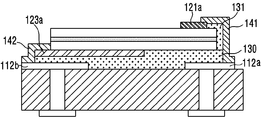
도 3은 본 발명의 제2 실시형태에 따른 반도체 발광장치의 단면을 개략적으로 나타내는 도면이다.3 is a schematic view showing a cross section of a semiconductor light emitting device according to a second embodiment of the present invention.
도 3을 참조하면, 본 실시형태에 따른 반도체 발광장치(200)는 적어도 일면 상에 형성된 제1 및 제2 전극패턴(112a, 112b)을 구비하는 기판(110)과, 상기 기판(110) 상에 배치되는 발광구조물(120)을 포함한다. 상기 발광구조물(120)은 제1 도전형 반도체층(121), 활성층(122) 및 제2 도전형 반도체층(123)을 포함하며, 상기 발광구조물(120)에는 제1 및 제2 도전형 반도체층(121, 123) 각각과 전기적으로 연결되는 제1 및 제2 전극구조(121a, 123a)가 형성될 수 있다.
3, the semiconductor
상기 제2 전극구조(123a)는 상기 기판(110)과 상기 발광구조물(120) 사이에 형성되어 상기 발광구조물(120)의 외측으로 연장되며, 상기 기판(110) 및 상기 제2 전극구조(123a) 사이에는, 상기 제2 전극구조(123a)를 기판(110)으로부터 분리하는 절연층(130)이 형성될 수 있다. 한편, 상기 기판(110) 상에 형성된 제1 및 제2 전극패턴(112a, 112b)은 제1 및 제2 연결부(141, 142)에 의해 상기 제1 및 제2 전극구조(121a, 123a) 각각과 전기적으로 연결될 수 있다.
The
본 실시형태에서는, 도 1 및 도 2에 도시된 실시형태와는 달리 제1 전극구조(121a)가 발광구조물(20) 상면에 형성됨으로써, 수직방향으로의 전류 흐름이 확대된 형태의 반도체 발광장치를 제공할 수 있다.1 and 2, the
도 1 및 도 2에 도시된 실시형태에 따른 반도체 발광장치(100, 101')의 경우 도전성 비아(v)를 이용하거나 발광구조물(20)을 메사 식각하여 이용하여 제1 전극구조(21a, 21a') 및 제2 전극구조(23a, 23a')가 모두 동일한 방향, 즉, 기판(10, 10')과 발광구조물(20, 20') 사이에 형성되었으나, 본 실시형태에서는 제1 및 제2 전극구조(121a, 123a)가 발광구조물(120)을 기준으로 서로 반대 방향을 향하도록 형성될 수 있다.
In the case of the semiconductor
구체적으로, 상기 제1 전극구조(121a)는 제1 도전형 반도체층(121) 상에 형성되며, 발광구조물(120)의 측면으로 연장되는 제1 연결부(141)에 의해 제1 전극패턴(112a)과 접속할 수 있다. 상기 제1 연결부(141)를 활성층(122) 및 제2 도전형 반도체층(123)과 전기적으로 분리하기 위하여, 상기 제1 연결부(141)와 발광구조물(120) 사이에는 절연층(131)이 형성될 수 있다.
Specifically, the
상기 발광구조물(20)과 기판(110) 사이에는 절연체(130)가 개재될 수 있으며, 상기 절연체(130)에 의해 상기 발광구조물(20)은 기판(110)과 안정적으로 결합할 수 있다. 상기 절연체(130)는 제1 실시형태와 마찬가지로 전기 절연성을 갖는 물체라면 어느 것이나 채용 가능하며, 예컨대, SiO2, SiOxNy, SixNy 등의 실리콘 산화물, 실리콘 질화물 등이 적용될 수 있을 것이다.
An
본 실시형태의 경우, 제1 및 제2 전극구조(121a, 123a)가 발광구조물의 상하면에 형성됨에 따라 수직 방향으로의 정류 흐름이 개선될 수 있으며, 도전성 비아 형성하기 위한 공정이 생략되어 공정을 단순화할 수 있다. 또한, 발광 영역인 활성층(122)이 제거되지 않아 발광 면적을 최대로 할 수 있으며, 발광구조물(120)과 기판(110) 사이에 제2 전극구조(123a)만이 형성되므로, 제2 전극구조(123a)의 형상 및 크기에 대한 설계 자유도가 증가한다.
In the case of this embodiment, since the first and
도 4는 본 발명의 제2 실시형태의 변형 예에 따른 반도체 발광장치의 단면을 개략적으로 나타낸 도면이다.4 is a schematic cross-sectional view of a semiconductor light emitting device according to a modification of the second embodiment of the present invention.
도 4를 참조하면, 본 실시형태에 따른 반도체 발광장치(200')는 적어도 일면 상에 형성된 제1 및 제2 전극패턴(112a', 112b')을 구비하는 기판(110')과, 상기 기판(110') 상에 배치되는 발광구조물(120')을 포함한다. 상기 발광구조물(120')은 제1 도전형 반도체층(121'), 활성층(122') 및 제2 도전형 반도체층(123')을 포함하며, 상기 발광구조물(120')에는 제1 및 제2 도전형 반도체층(121', 123') 각각과 전기적으로 연결되는 제1 및 제2 전극구조(121a', 123a')가 형성될 수 있다.
Referring to FIG. 4, the semiconductor light emitting device 200 'according to the present embodiment includes a substrate 110' having first and
본 실시형태의 경우, 제1 및 제2 전극구조(121a', 123a')가 발광구조물(120')을 기준으로 하여 서로 반대인 면에 수직 방향으로 형성된다는 점에서 도 3에 도시된 반도체 발광장치(200)와 유사하나, 발광구조물(120')과 기판(110') 사이에 형성되는 도전성 기판(160') 및 도전성 비아(v)와, 제1 전극구조(121a')와 연결되는 도전형 컨택층(121b')을 더 포함한다는 점에서 차이가 존재한다.
In this embodiment, since the first and
구체적으로, 상기 도전성 기판(160')은 레이저 리프트 오프 등의 공정에서 상기 발광구조물을 지지하는 지지체의 역할을 수행하며, Au, Ni, Al, Cu, W, Si, Se, GaAs 중 하나 이상을 포함하는 물질, 예컨대, Si에 Al이 도핑된 형태의 물질로 이루어질 수 있다. 이 경우, 선택된 물질에 따라, 도전성 기판(160')은 도금 또는 본딩 접합 등의 방법으로 형성될 수 있을 것이다.Specifically, the conductive substrate 160 'serves as a support for supporting the light emitting structure in a process such as laser lift-off, and at least one of Au, Ni, Al, Cu, W, Si, Se, For example, a material in the form of Al doped with Si. In this case, depending on the selected material, the conductive substrate 160 'may be formed by a method such as plating or bonding.
따라서, 이에 제한되는 것은 아니나, 본 실시형태의 경우 상기 제1 및 제2 도전형 반도체층(121', 123')은 이전 실시형태와는 달리 각각 p형 및 n형 반도체층으로 이해될 수 있을 것이다.
Accordingly, although not limited thereto, the first and second conductivity type semiconductor layers 121 'and 123' may be understood as p-type and n-type semiconductor layers, respectively, unlike the previous embodiments will be.
상기 도전성 기판(160')은 제2 도전형 반도체층(123')과 전기적으로 연결되며, 이에 따라, 도전성 기판(160')을 통하여 제2 도전형 반도체층(123')에 전기 신호가 인가되는 전극으로 기능할 수 있다. 이를 위하여, 도 4에 도시된 것과 같이, 도전성 기판(160')으로부터 연장되어 제2 도전형 반도체층(23)과 접속된 도전성 비아(v)가 구비될 수 있으며, 상기 제1 전극구조(123a')는 상기 도전성 기판(160')과 일체로 형성될 수 있다.
The conductive substrate 160 'is electrically connected to the second conductive semiconductor layer 123' so that an electric signal is applied to the second conductive semiconductor layer 123 'through the conductive substrate 160' As shown in Fig. 4, a conductive vias v extending from the conductive substrate 160 'and connected to the second conductive
본 실시형태에서 도전성 비아(v)의 개수, 형상, 피치, 제2 도전형 반도체층(23)과의 접촉 면적은 적절히 조절될 수 있으며, 상기 도전성 비아(v)와 도전성 기판(160') 또한 일체로 형성될 수 있다. 상기 도전성 비아(v)와 발광구조물(120') 사이에는, 도전성 비아(v)를 활성층(122') 및 제1 도전형 반도체층(121')과 전기적으로 분리시키기 위한 절연층(131')이 개재될 수 있다.In the present embodiment, the number, shape, pitch, and contact area of the conductive vias v with the second conductive
한편, 상기 발광구조물(120')과 기판(110') 사이에는 도전형 컨택층(121b')이 형성될 수 있으며, 도전형 컨택층(121b')은 활성층(122')에서 방출된 빛을 제2 도전형 반도체층(123') 방향으로 반사하는 기능을 수행할 수 있다. 상기 도전형 컨택층(121b')은 전기적으로 도전성 기판(160')과 분리되며, 이를 위하여 도전형 컨택층(121b')과 도전성 기판(160') 사이에는 절연체(131')가 개재될 수 있다.
A conductive contact layer 121b 'may be formed between the light emitting structure 120' and the substrate 110 ', and the conductive contact layer 121b' may include light emitted from the active layer 122 ' And to reflect the light toward the second conductivity type semiconductor layer 123 '. The conductive type contact layer 121b 'is electrically isolated from the conductive substrate 160', and an insulator 131 'may be interposed between the conductive type contact layer 121b' and the conductive substrate 160 ' have.
도 5 내지 도 9는 본 발명의 일 실시형태에 따른 반도체 발광장치의 제조방법을 설명하기 위한 도면으로, 구체적으로, 도 1에 도시된 구조의 반도체 발광장치(100)를 제조하기 위한 공정에 해당한다.5 to 9 are views for explaining a method of manufacturing a semiconductor light emitting device according to an embodiment of the present invention. Specifically, FIG. 5 to FIG. 9 correspond to the steps for manufacturing the semiconductor
도 5 내지 도 9에서는 제1 및 제2 전극구조를 갖는 하나의 반도체 발광장치를 기준으로 도시하였으나 이에 제한되는 것은 아니며, 웨이퍼 레벨에서 복수 개의 소자 단위 발광장치를 제조하는 공정 중에도 적용될 수 있을 것이다.
Although FIGS. 5 to 9 show one semiconductor light emitting device having the first and second electrode structures as a reference, the present invention is not limited thereto, and may be applied to a process for manufacturing a plurality of device light emitting devices at a wafer level.
본 실시형태에 따른 반도체 발광장치의 제조방법은, 반도체 성장용 기판(50) 상에 발광구조물(20)을 형성하는 단계와, 상기 발광구조물(20)에 제1 및 제2 전극구조(21a, 23a)를 형성하는 단계와, 제1 및 제2 전극패턴(12a, 12b)을 구비하는 기판 상에 상기 발광구조물(20)을 부착하는 단계와, 상기 발광구조물(20)로부터 상기 반도체 성장용 기판(50)을 제거하는 단계와, 상기 발광구조물(20)의 일부를 제거하여 상기 제2 전극패턴(12b)을 노출시키는 단계와, 상기 제1 및 제2 전극패턴(12a, 12b)과 제1 및 제2 전극구조(12a, 12b)를 연결하는 제1 및 제2 연결부(41, 42)를 형성하는 단계를 포함할 수 있다.
The method for manufacturing a semiconductor light emitting device according to the present embodiment includes the steps of forming a
우선, 도 5에 도시된 바와 같이 반도체 성장용 기판(50) 상에 제1 도전형 반도체층(21), 활성층(22) 및 제2 도전형 반도체층(23)을 MOCVD, MBE, HVPE 등과 같은 반도체층 성장 공정을 이용하여 순차적으로 성장시켜 발광구조물(20)을 형성할 수 있다. 예를 들면, 상기 발광구조물(20)은 AlxInyGa(1-x-y)N(0≤x≤1, 0≤y≤1, 0≤x+y≤1)의 조성을 갖는 질화물계 반도체로 구성될 수 있다.
5, the first conductivity
반도체 성장용 기판(10)은 사파이어, SiC, MgAl2O4, MgO, LiAlO2, LiGaO2, GaN 등의 물질로 이루어진 기판을 사용할 수 있다. 이 경우, 사파이어는 육각-롬보형(Hexa-Rhombo R3c) 대칭성을 갖는 결정체로서 c축 및 a축 방향의 격자상수가 각각 13.001Å과 4.758Å이며, C(0001)면, A(1120)면, R(1102)면 등을 갖는다. 이 경우, 상기 C면은 비교적 질화물 박막의 성장이 용이하며, 고온에서 안정하기 때문에 질화물 성장용 기판으로 주로 사용된다. 구체적으로 도시하지는 않았으나, 상기 발광구조물(20)과 반도체 성장용 기판(10) 사이에는 버퍼층이 형성될 수 있으며, 버퍼층은 질화물 등으로 이루어진 언도프 반도체층으로 채용되어, 그 위에 성장되는 발광구조물의 격자 결함을 완화할 수 있다.
The
상기 발광구조물(20) 상에는 상기 제1 및 제2 도전형 반도체층(21, 23) 각각과 전기적으로 연결되는 제1 및 제2 전극구조(21a, 23a)가 형성될 수 있다. 상기 제1 및 제2 전극구조(21a, 23a)는 상기 발광구조물(20)의 동일한 방향에 형성될 수 있다. 상기 제1 및 제2 전극구조(21a, 23a)는 광 반사 기능과 반도체층과의 오믹 컨택 기능을 고려하여 Ag, Ni, Cr, Ti, Al, Rh, Pd, Ir, Ru, Mg, Zn, Pt, Au 등의 물질을 포함하도록 형성할 수 있으며, 당 기술 분야에서 공지된 스퍼터링이나 증착 등의 공정을 적절히 이용할 수 있다.First and
구체적으로 도시하지는 않았으나, 제1 및 제2 전극구조(21a, 23a)는 2층 이상의 구조로 채용되어 반사 효율을 향상시킬 수 있으며, 예를 들면, Ni/Ag, Zn/Ag, Cr/Au, Cr/Al, Ti/Al, Ni/Al, Zn/Al, Pd/Ag, Pd/Al, Ir/Ag. Ir/Au, Pt/Ag, Pt/Al, Ni/Ag/Pt 등을 들 수 있다.
The first and
상기 제1 전극구조(21a)는 상기 제2 도전형 반도체층(23)과 활성층(22)을 관통하여 제1 도전형 반도체층(21)과 접속하는 도전성 비아(v)를 포함할 수 있다. 상기 도전성 비아(v)는 상기 발광구조물(20)의 일부를 제거하여 형성된 홈 내부를 도전성 물질, 예를 들면, Ti, TiW, Au, Ni, Al, Cu, W, Si, Se, GaAs 중 어느 하나를 포함하는 물질로 충전하여 형성할 수 있다. 이때, 도금, 스퍼터링, 증착 등의 공정이 이용될 수 있으며, 도전성 비아(v)의 개수, 형상, 피치 등은 필요에 따라 적절히 조절될 수 있을 것이다.The
상기 도전성 비아(v)를 포함하는 제1 전극구조(21a)를 활성층(22) 및 제2 도전형 반도체층(23)과 전기적으로 분리하기 위하여, 그 사이에는 절연층(31)이 개재될 수 있으며, 상기 절연층(31)은 발광구조물(20) 표면에 SiO2, SiOxNy, SixNy 등과 같은 물질을 증착시켜 형성할 수 있다.
In order to electrically isolate the
다음으로, 도 6에 도시된 바와 같이, 절연체(30)를 이용하여 상기 발광구조물(20)을 기판(10)에 부착할 수 있다. 상기 기판(10)은 적어도 일면에 형성된 제1 및 제2 전극패턴(12a, 12b)을 구비하며, 상기 발광구조물(20)은 제2 전극구조(21a, 23a)가 형성된 면이 상기 기판(10)을 향하도록 배치될 수 있다. Next, as shown in FIG. 6, the
상기 기판(10)은, 기판 본체(11)와 상기 기판 본체(11)의 상면에 형성된 제1 및 제2 전극패턴(12a, 12b)과, 상기 기판 본체(11)를 두께 방향으로 관통하는 복수의 비아(14)와, 상기 기판 본체(11)의 하면에 형성된 하부 전극(13)을 포함할 수 있다. 다만, 기판(10)의 형상이 이에 제한되는 것은 아니며, 본 실시형태에 적용될 수 있는 기판(10)은, 발광구조물(20)이 배치되는 면과 그 대향하는 면 모두에 발광구조물을 구동하기 위한 배선 구조가 형성된 기판이라면 어느 것이나 적용 가능하다.
The
본 실시형태에서, 상기 발광구조물(20)은 제2 전극구조(23a)가 형성된 면이 상기 기판(10)의 제1 및 제2 전극패턴(12a, 12b)과 마주보는 형태로, 상기 발광구조물(20)과 기판(10) 사이에 개재되는 절연체(30)에 의해 상기 기판(10)에 고정될 수 있다.The
절연체(30)는 제1 및 제2 전극구조(21a, 23a)를 서로 전기적으로 분리함과 동시에, 발광구조물(20)과 기판(10)을 안정적으로 결합시킬 수 있다. 절연체(30)는 전기 절연성을 갖는 물체라면 어느 것이나 채용 가능하지만, 빛을 최소한으로 흡수하는 것이 바람직하므로, 예컨대, SiO2, SiOxNy, SixNy 등의 실리콘 산화물, 실리콘 질화물을 이용할 수 있을 것이다.
The
상기 절연체(30)는 상기 발광구조물(20) 및 기판(10) 중 적어도 하나의 표면에 증착, SOG(Spin On Glass), 도포 등의 다양한 공지된 방법을 이용하여 형성될 수 있다. 예를 들면, 유동성이 있는 수지를 기판(10) 또는 발광구조물(20) 표면에 도포 후 경화시키는 공정을 통해 발광구조물(20)과 기판(10)을 부착하거나, 발광구조물(20) 및 기판(10) 표면에 수지 도포 후 수지가 경화된 상태에서 수지가 형성된 면을 상호 접촉시켜 열과 압력을 가해줌으로써 수지와 수지 사이를 결합시키는 방법도 가능하다.The
이에 따라, 상기 발광구조물(20) 상에 형성된 제1 및 제2 전극구조(21a, 23a)는 상기 절연체(30)에 의해 기판(10)의 제1 및 제2 전극패턴(12a, 12b)과 분리될 수 있다.
The first and
일반적으로, 제1 및 제2 전극구조(21a, 23a)가 상기 제1 및 제2 전극패턴(12a, 12b)과 접촉한 상태에서 용융됨으로써 상기 발광구조물(20)이 상기 기판(10)에 고정되는 경우, 용융된 제1 및 제2 전극구조(21a, 23a)가 서로 닿아 쇼트에 의한 불량이 발생할 수 있다. 한편, 이러한 현상을 방지하기 위하여 제1 및 제2 전극구조(21a, 23a)는 서로 일정 간격을 두고 이격 배치될 수 있으나, 이러한 경우에는 발광구조물(20)과 기판(10) 사이의 접촉 면적이 좁아져 발광구조물(20)과 기판(10) 사이의 결합력이 약해지는 문제가 있다.
The
그러나, 본 실시형태의 경우, 발광구조물(20)과 기판(10)이 제1 및 제2 전극구조(21a, 23a)를 매개로 결합하는 것이 아니라 별도의 절연체(30)를 이용하여 결합하게 되므로 상술한 문제점들을 해결하여 신뢰성이 개선된 반도체 발광장치를 제공할 수 있다. 구체적으로, 본 실시형태에 따른 반도체 발광장치 제조방법은 절연체(30)를 이용하여 제1 및 제2 전극구조(21a, 23a)를 전기적으로 분리할 뿐만 아니라, 절연체(30)를 접착 물질로 이용함으로써 기판(10)과 발광구조물(20)이 안정적이고 견고하게 결합하도록 할 수 있다.
However, in the case of the present embodiment, the
다음으로, 도 7에 도시된 바와 같이 상기 기판(10)이 부착된 발광구조물(20)로부터 반도체 성장용 기판(50)을 제거할 수 있다. 이때, 상기 기판(10)은 반도체 성장용 기판(50)을 제거 시 지지기판으로 기능할 수 있으며, 반도체 성장용 기판(50)은 레이저 리프트 오프나 화학적 리프트 오프 등과 같은 공정을 이용하여 제거될 수 있다.
Next, as shown in FIG. 7, the
다음으로, 도 8에 도시된 바와 같이, 발광구조물(20) 및 절연체(30)의 일부를 제거하여 상기 제1 및 제2 전극패턴(12b)의 적어도 일부를 노출시킬 수 있다. 상기 발광구조물(20)과 절연체(30)를 제거하는 공정은 동시에 이루어지거나, 또는 서로 분리하여 순차적으로 이루어질 수 있으며, 당 기술분야에서 공지된 식각 공정, 예컨대, ICP-RIE 등을 이용하여 수행될 수 있다. 식각 공정을 통해 상기 제1 및 제2 전극패턴(12a, 12b)의 노출된 영역은, 추후 제1 및 제2 도전형 반도체층(21, 23)과의 전기 연결부로 제공될 수 있다.Next, as shown in FIG. 8, the
한편, 본 공정이 웨이퍼 레벨로 수행되는 경우, 상기 발광구조물(20)의 일부를 제거하는 공정은 상기 발광구조물(20)을 개별 소자 단위로 분리하는 공정과 동시에 진행될 수 있을 것이다.
Meanwhile, when the present process is performed at a wafer level, a process of removing a part of the
다음으로, 도 9에 도시된 바와 같이, 노출된 상기 제1 및 제2 전극패턴(12a, 12b)과 제1 및 제2 전극구조(21a, 23a) 각각을 연결하는 제1 및 제2 연결부(41, 42)를 형성할 수 있다.Next, as shown in FIG. 9, the first and second connection portions (12a, 12b) connecting the exposed first and
상기 제1 및 제2 연결부(41, 42)는 상기 제1 및 제2 전극패턴(12a, 12b)의 노출된 영역으로부터 상기 제1 및 제2 전극구조(21a, 23a)로 연장되도록 형성될 수 있다. 구체적으로, 상기 제1 및 제2 연결부(41, 42)는 상기 발광구조물(20)의 외측으로 연장되어 노출되는 제1 및 제2 전극구조(21a, 23a)와 접촉하여 상기 기판(10)을 통해 상기 발광구조물(20)에 전기 신호를 인가할 수 있다. 이를 위하여 상기 제1 및 제2 연결부(41, 42)는 전기 전도성이 우수한 금속 물질로 이루어질 수 있으며, 공지된 도금, 증착 등의 방법을 이용하여 형성될 수 있다.
The first and
도 10 내지 도 15는 본 발명의 다른 실시형태에 따른 반도체 발광장치의 제조방법을 설명하기 위한 도면으로, 구체적으로, 도 3에 도시된 구조의 반도체 발광장치(100)를 제조하기 위한 공정에 해당한다.10 to 15 are views for explaining a method of manufacturing the semiconductor light emitting device according to another embodiment of the present invention. Specifically, FIG. 10 to FIG. 15 are views for explaining the method for manufacturing the semiconductor
이전 실시형태와 마찬가지로, 도 10 내지 도 15에서는 제1 및 제2 전극구조를 갖는 하나의 반도체 발광장치를 기준으로 도시하였으나 이에 제한되는 것은 아니며, 웨이퍼 레벨에서 복수 개의 소자 단위 발광장치를 제조하는 공정 중에도 적용될 수 있을 것이다.
10 to 15, one semiconductor light emitting device having the first and second electrode structures is shown as a reference, but the present invention is not limited thereto, and a process for manufacturing a plurality of device light emitting devices at a wafer level .
본 실시형태에 따른 반도체 발광장치의 제조방법은, 반도체 성장용 기판(150) 상에 발광구조물(120)을 형성하는 단계와, 상기 발광구조물(120)에 제1 및 제2 전극구조(121a, 123a)를 형성하는 단계와, 제1 및 제2 전극패턴(112a, 112b)을 구비하는 기판(110) 상에 절연체(130)를 이용하여 상기 발광구조물(120)을 부착하는 단계와, 상기 발광구조물(120)로부터 상기 반도체 성장용 기판(150)을 제거하는 단계와, 상기 발광구조물(120) 및 절연체(130)의 일부를 제거하여 상기 제1 및 제2 전극패턴(112a, 112b)의 적어도 일부를 노출시키는 단계와, 상기 제1 및 제2 전극패턴(112a, 112b)과 제1 및 제2 전극구조(112a, 112b)를 연결하는 제1 및 제2 연결부(141, 142)를 형성하는 단계를 포함할 수 있다.
The method of manufacturing a semiconductor light emitting device according to the present embodiment includes the steps of forming a
우선, 도 10에 도시된 바와 같이 반도체 성장용 기판(150) 상에 제1 도전형 반도체층(121), 활성층(122) 및 제2 도전형 반도체층(123)을 순차적으로 적층하여 발광구조물(120)을 형성할 수 있다. 상기 반도체 성장용 기판(150)은 사파이어, SiC, MgAl2O4, MgO, LiAlO2, LiGaO2, GaN 등의 물질로 이루어진 기판을 사용할 수 있으며, 상기 발광구조물(120)은 MOCVD, MBE, HVPE 등과 같은 반도체층 성장 공정을 이용하여 상기 반도체 성장용 기판(150) 상에서 성장될 수 있다.
10, a first conductivity
상기 발광구조물(120) 상면에는 제2 도전형 반도체층(123)과 전기적으로 연결되도록 제2 전극구조(123a)가 형성될 수 있다. 상기 제2 전극구조(123a)는 광 반사 기능과 제2 도전형 반도체층(123)과의 오믹 컨택 기능을 고려하여 Ag, Ni, Al, Rh, Pd, Ir, Ru, Mg, Zn, Pt, Au 등의 물질을 포함하도록 형성할 수 있으며, 당 기술 분야에서 공지된 스퍼터링이나 증착 등의 공정을 적절히 이용할 수 있다.
A
다음으로, 도 11에 도시된 바와 같이, 절연체(130)를 이용하여 상기 발광구조물(120)을 기판(110)에 부착할 수 있다. 상기 기판(110)의 일면에는 제1 및 제2 전극패턴(112a, 112b)을 구비할 수 있으며, 상기 제1 및 제2 전극패턴(112a, 112b)은 기판 본체(111)를 두께 방향으로 관통하는 도전성 비아(114)에 의해 하부 전극(113)과 연결될 수 있다. 상기 발광구조물(120)은 상기 제2 전극구조(123a)가 형성된 면이 상기 기판(110)을 마주보도록 배치될 수 있으며, 상기 제2 전극구조(123a)는 상기 절연체(130)에 의해 상기 기판(110)의 제2 전극패턴(112b)과 분리될 수 있다.
Next, as shown in FIG. 11, the
다음으로, 도 12에 도시된 바와 같이, 상기 기판(110)이 부착된 발광구조물(120)로부터 반도체 성장용 기판(150)을 제거할 수 있다. 상기 반도체 성장용 기판(150)은 상기 기판(110)을 지지체로 하여 화학적 또는 레이저 리프트 오프를 통해 제거될 수 있다.
Next, as shown in FIG. 12, the
다음으로, 도 13에 도시된 바와 같이, 상기 발광구조물(120) 및 절연체(130)의 일부를 제거하여 상기 제1 및 제2 전극패턴(112a, 112b)의 적어도 일부를 노출시킬 수 있다. 이전 실시형태에서도 설명한 바와 같이, 상기 발광구조물(120) 및 절연체(130)의 일부를 제거하는 공정은 웨이퍼 레벨로 발광구조물을 개별 소자단위를 분리하는 공정 중에 이루어질 수 있다.Next, as shown in FIG. 13, at least a part of the first and
한편, 상기 발광구조물(120)의 측면 및 상면의 일부에는, 제1 전극구조(미도시)와 제1 전극패턴(112a)을 연결하는 제1 연결부(미도시)가 형성될 영역에 절연체(131)가 형성될 수 있다. 상기 절연체(131)는 상기 제1 연결부를 제2 도전형 반도체층(123) 및 활성층(122)과 전기적으로 분리하기 위한 것으로, 도 13에 도시된 것과 달리, 상기 발광구조물(120)의 측면만을 덮는 형태로 형성되는 것도 가능하다.
An insulator 131 (not shown) is formed in a region where a first connection structure (not shown) for connecting the first electrode structure (not shown) and the
다음으로, 도 14에 도시된 바와 같이, 상기 제1 도전형 반도체층(121) 상에 제1 전극구조(121a)를 형성할 수 있다. 상기 제1 전극구조(121a)는 상기 제1 도전형 반도체층(121)에 외부 전기 신호를 인가하기 위한 전극 패드로 기능할 수 있다.Next, as shown in FIG. 14, a
이를 위하여, 도 15에 도시된 바와 같이 상기 제1 전극패드(112a)로부터 발광구조물(120)의 측면으로 연장되어 상기 제1 전극구조(121a)와 접속하는 제1 연결부(141)와, 상기 제2 전극구조(123a)를 제2 전극패턴(112b)과 연결하는 제2 연결부(142)를 형성할 수 있다. 이로써, 상기 제1 및 제2 도전형 반도체층(121, 123) 각각과 전기적으로 연결되는 제1 및 제2 전극구조(121a, 123a)는 상기 제1 및 제2 연결부(141, 142)에 의해 상기 기판(110)의 제1 및 제2 전극패턴(112a, 112b)과 접속하여 외부 신호를 인가받을 수 있다.
15, a
본 실시형태에 따른 반도체 발광소자의 제조방법의 경우, 절연체(30, 130)를 발광구조물(20, 120)과 기판(10, 110)을 결합시키는 접착 물질로 이용하며, 이로써 간단한 공정을 통해 기판(10, 110)과 발광구조물(20, 120)이 안정적이고 견고하게 결합하도록 할 수 있다. 또한, 쇼트 발생 위험이 없고, 발광소자 실장 기판과의 견고한 결합이 가능하므로 신뢰성이 개선된 반도체 발광장치를 제공할 수 있다.
In the method of manufacturing a semiconductor light emitting device according to the present embodiment, the
100, 200: 반도체 발광장치 10, 110: 기판
11, 111: 기판 본체 12a, 112a: 제1 전극패턴
12b, 112b: 제2 전극패턴 13, 113: 하부전극
14, 114: 도전성 비아 20, 120: 발광구조물
21, 121: 제1 도전형 반도체층 22, 122: 활성층
23, 123: 제2 도전형 반도체층 21a, 121a: 제1 전극구조
23a, 123a: 제2 전극구조 30, 130: 절연체
31, 131: 절연층 41, 141: 제1 연결부
42, 142: 제2 연결부 50, 150: 반도체 성장용 기판 100, 200: semiconductor
11, 111:
12b, 112b:
14, 114:
21, 121: first conductivity
23, 123: second conductivity
23a, 123a:
31, 131: insulating
42, 142:
Claims (23)
상기 기판의 일면 상에 배치되며, 제1 도전형 반도체층, 활성층 및 제2 도전형 반도체층을 포함하는 발광구조물;
상기 제1 도전형 반도체층과 전기적으로 연결되도록 형성되는 제1 전극구조;
상기 제2 도전형 반도체층과 전기적으로 연결되며 상기 기판과 상기 발광구조물 사이에 형성되어 상기 발광구조물의 외측으로 연장되는 제2 전극구조;
상기 기판 및 제2 전극구조 사이에 개재되어 상기 기판과 상기 제2 전극구조를 분리하는 절연층;
상기 제1 전극구조와 상기 제1 전극패턴을 연결하는 제1 연결부; 및
상기 절연층의 외측면 상으로 연장되어, 상기 발광구조물의 외측으로 연장된 제2 전극구조와 상기 제2 전극패턴을 연결하는 제2 연결부;
를 포함하는 반도체 발광장치.
A substrate having first and second electrode patterns formed on at least one surface thereof;
A light emitting structure disposed on one surface of the substrate, the light emitting structure including a first conductive semiconductor layer, an active layer, and a second conductive semiconductor layer;
A first electrode structure formed to be electrically connected to the first conductivity type semiconductor layer;
A second electrode structure electrically connected to the second conductivity type semiconductor layer, the second electrode structure being formed between the substrate and the light emitting structure and extending outside the light emitting structure;
An insulating layer interposed between the substrate and the second electrode structure to separate the substrate from the second electrode structure;
A first connection unit connecting the first electrode structure and the first electrode pattern; And
A second connection part extending on the outer surface of the insulating layer and connecting the second electrode structure to the second electrode structure extending outside the light emitting structure;
And a semiconductor light emitting device.
상기 제1 전극구조는 상기 제2 도전형 반도체층 및 활성층을 관통하여 상기 제1 도전형 반도체층과 접속하는 도전성 비아를 포함하는 것을 특징으로 하는 반도체 발광장치.
The method according to claim 1,
Wherein the first electrode structure includes a conductive via penetrating through the second conductive type semiconductor layer and the active layer and connected to the first conductive type semiconductor layer.
상기 도전성 비아를 상기 제2 도전형 반도체층 및 상기 활성층과 분리시키기 위한 절연체를 더 포함하는 것을 특징으로 하는 반도체 발광장치.
3. The method of claim 2,
Further comprising an insulator for separating the conductive via from the second conductive type semiconductor layer and the active layer.
상기 제1 전극구조는 상기 발광구조물과 상기 기판 사이에 형성되며, 상기 절연층에 의해 상기 기판과 분리되는 것을 특징으로 하는 반도체 발광장치.
The method according to claim 1,
Wherein the first electrode structure is formed between the light emitting structure and the substrate, and is separated from the substrate by the insulating layer.
상기 기판의 일면 상에 배치되며, 제1 도전형 반도체층, 활성층 및 제2 도전형 반도체층을 포함하는 발광구조물;
상기 제1 도전형 반도체층과 전기적으로 연결되도록 형성되는 제1 전극구조;
상기 제2 도전형 반도체층과 전기적으로 연결되며 상기 기판과 상기 발광구조물 사이에 형성되어 상기 발광구조물의 외측으로 연장되는 제2 전극구조;
상기 기판 및 제2 전극구조 사이에 개재되어 상기 기판과 상기 제2 전극구조를 분리하는 절연층;
상기 제1 전극구조와 상기 제1 전극패턴을 연결하는 제1 연결부; 및
상기 발광구조물의 외측으로 연장된 제2 전극구조와 상기 제2 전극패턴을 연결하는 제2 연결부;
를 포함하고,
상기 제1 전극구조는 상기 발광구조물 및 상기 기판 사이에서 상기 발광구조물의 외측으로 연장되는 것을 특징으로 하는 반도체 발광장치.
A substrate having first and second electrode patterns formed on at least one surface thereof;
A light emitting structure disposed on one surface of the substrate, the light emitting structure including a first conductive semiconductor layer, an active layer, and a second conductive semiconductor layer;
A first electrode structure formed to be electrically connected to the first conductivity type semiconductor layer;
A second electrode structure electrically connected to the second conductivity type semiconductor layer, the second electrode structure being formed between the substrate and the light emitting structure and extending outside the light emitting structure;
An insulating layer interposed between the substrate and the second electrode structure to separate the substrate from the second electrode structure;
A first connection unit connecting the first electrode structure and the first electrode pattern; And
A second connection part connecting a second electrode structure extending outside the light emitting structure and the second electrode pattern;
Lt; / RTI >
Wherein the first electrode structure extends to the outside of the light emitting structure between the light emitting structure and the substrate.
상기 제1 연결부는 상기 제1 전극구조 중 상기 발광구조물의 외측으로 연장된 영역 및 상기 제1 전극패턴과 접촉하도록 형성된 것을 특징으로 하는 반도체 발광장치.
6. The method of claim 5,
Wherein the first connection portion is formed to be in contact with a region of the first electrode structure extending outside the light emitting structure and the first electrode pattern.
상기 제1 전극구조는 상기 발광구조물에서 상기 기판과 마주하는 면과 반대인 면에 형성된 것을 특징으로 하는 반도체 발광장치.
The method according to claim 1,
Wherein the first electrode structure is formed on a surface of the light emitting structure opposite to a surface facing the substrate.
상기 제1 연결부는 상기 제1 전극구조로부터 상기 발광구조물의 측면으로 연장되어 상기 제1 전극패턴과 접촉하도록 형성된 것을 특징으로 하는 반도체 발광장치.
8. The method of claim 7,
Wherein the first connection part extends from the first electrode structure to a side of the light emitting structure and is configured to contact the first electrode pattern.
상기 제1 및 제2 도전형 반도체층과 각각 전기적으로 연결되는 제1 및 제2 전극구조를 형성하는 단계;
적어도 일면에 제1 및 제2 전극패턴을 구비하는 기판을 마련하는 단계;
상기 발광구조물의 상기 제2 전극구조가 형성된 면과 상기 기판의 상기 제1 및 제2 전극패턴이 형성된 면 사이에 개재되는 절연체를 이용하여 상기 발광구조물과 상기 기판을 부착하는 단계;
상기 발광구조물로부터 상기 반도체 성장용 기판을 제거하는 단계;
상기 발광구조물 및 상기 절연체의 일부를 제거하여 상기 제1 및 제2 전극패턴의 적어도 일부를 노출시키는 단계; 및
상기 제1 및 제2 전극구조를 상기 제1 및 제2 전극패턴 각각과 전기적으로 연결하는 제1 및 제2 연결부를 형성하는 단계;
를 포함하는 반도체 발광장치 제조방법.
Providing a light emitting structure in which a first conductivity type semiconductor layer, an active layer, and a second conductivity type semiconductor layer are sequentially stacked on a substrate for semiconductor growth;
Forming first and second electrode structures electrically connected to the first and second conductivity type semiconductor layers, respectively;
Providing a substrate having first and second electrode patterns on at least one surface thereof;
Attaching the light emitting structure and the substrate using an insulator interposed between a surface of the light emitting structure on which the second electrode structure is formed and a surface of the substrate on which the first and second electrode patterns are formed;
Removing the semiconductor growth substrate from the light emitting structure;
Exposing at least a portion of the first and second electrode patterns by removing a portion of the light emitting structure and the insulator; And
Forming first and second connection portions electrically connecting the first and second electrode structures to the first and second electrode patterns, respectively;
Wherein the semiconductor light emitting device is a semiconductor light emitting device.
상기 기판의 일면에 상기 발광구조물을 부착하는 단계에서 상기 절연체는 유동성을 갖는 것을 특징으로 하는 반도체 발광장치 제조방법.10. The method of claim 9,
Wherein the insulator has fluidity in the step of attaching the light emitting structure to one surface of the substrate.
Priority Applications (3)
| Application Number | Priority Date | Filing Date | Title |
|---|---|---|---|
| KR1020120033978A KR101891257B1 (en) | 2012-04-02 | 2012-04-02 | Light Emitting Device and Manufacturing Method thereof |
| US13/803,943 US8946760B2 (en) | 2012-04-02 | 2013-03-14 | Semiconductor light emitting device and fabrication method thereof |
| US14/576,667 US9236525B2 (en) | 2012-04-02 | 2014-12-19 | Semiconductor light emitting device and fabrication method thereof |
Applications Claiming Priority (1)
| Application Number | Priority Date | Filing Date | Title |
|---|---|---|---|
| KR1020120033978A KR101891257B1 (en) | 2012-04-02 | 2012-04-02 | Light Emitting Device and Manufacturing Method thereof |
Publications (2)
| Publication Number | Publication Date |
|---|---|
| KR20130111800A KR20130111800A (en) | 2013-10-11 |
| KR101891257B1 true KR101891257B1 (en) | 2018-08-24 |
Family
ID=49233717
Family Applications (1)
| Application Number | Title | Priority Date | Filing Date |
|---|---|---|---|
| KR1020120033978A Expired - Fee Related KR101891257B1 (en) | 2012-04-02 | 2012-04-02 | Light Emitting Device and Manufacturing Method thereof |
Country Status (2)
| Country | Link |
|---|---|
| US (2) | US8946760B2 (en) |
| KR (1) | KR101891257B1 (en) |
Cited By (1)
| Publication number | Priority date | Publication date | Assignee | Title |
|---|---|---|---|---|
| WO2021075728A1 (en) * | 2019-10-15 | 2021-04-22 | Samsung Electronics Co., Ltd. | Display module and manufacturing method thereof |
Families Citing this family (58)
| Publication number | Priority date | Publication date | Assignee | Title |
|---|---|---|---|---|
| US9899329B2 (en) | 2010-11-23 | 2018-02-20 | X-Celeprint Limited | Interconnection structures and methods for transfer-printed integrated circuit elements with improved interconnection alignment tolerance |
| US8934259B2 (en) | 2011-06-08 | 2015-01-13 | Semprius, Inc. | Substrates with transferable chiplets |
| WO2013187723A1 (en) * | 2012-06-14 | 2013-12-19 | An Sang Jeong | Semiconductor light-emitting element and production method therefor |
| KR101494331B1 (en) * | 2013-12-11 | 2015-02-23 | 한국광기술원 | Flip chip type nitride semiconductor light emitting device |
| DE102014102029A1 (en) | 2014-02-18 | 2015-08-20 | Osram Opto Semiconductors Gmbh | Process for the production of semiconductor devices and semiconductor device |
| TWI814461B (en) | 2014-06-18 | 2023-09-01 | 愛爾蘭商艾克斯展示公司技術有限公司 | Micro assembled led displays and lighting elements |
| US9716082B2 (en) | 2014-08-26 | 2017-07-25 | X-Celeprint Limited | Micro assembled hybrid displays and lighting elements |
| US9799719B2 (en) | 2014-09-25 | 2017-10-24 | X-Celeprint Limited | Active-matrix touchscreen |
| US9818725B2 (en) | 2015-06-01 | 2017-11-14 | X-Celeprint Limited | Inorganic-light-emitter display with integrated black matrix |
| US9991163B2 (en) | 2014-09-25 | 2018-06-05 | X-Celeprint Limited | Small-aperture-ratio display with electrical component |
| US9799261B2 (en) | 2014-09-25 | 2017-10-24 | X-Celeprint Limited | Self-compensating circuit for faulty display pixels |
| KR101629268B1 (en) | 2014-10-29 | 2016-06-10 | 엘지전자 주식회사 | Display device using semiconductor light emitting device and method of fabricating the same |
| KR102014258B1 (en) * | 2014-11-21 | 2019-08-26 | 엘지전자 주식회사 | Display device using semiconductor light emitting device and method of fabricating the same |
| DE102015107526A1 (en) * | 2015-05-13 | 2016-11-17 | Osram Opto Semiconductors Gmbh | Optoelectronic semiconductor chip and optoelectronic module |
| CN106298837A (en) * | 2015-05-29 | 2017-01-04 | 鸿富锦精密工业(深圳)有限公司 | OLED display panel and splicing display device |
| KR20160141301A (en) * | 2015-05-29 | 2016-12-08 | 삼성전자주식회사 | Semiconductor light emitting device package |
| US9871345B2 (en) | 2015-06-09 | 2018-01-16 | X-Celeprint Limited | Crystalline color-conversion device |
| US10133426B2 (en) | 2015-06-18 | 2018-11-20 | X-Celeprint Limited | Display with micro-LED front light |
| US11061276B2 (en) | 2015-06-18 | 2021-07-13 | X Display Company Technology Limited | Laser array display |
| US10255834B2 (en) | 2015-07-23 | 2019-04-09 | X-Celeprint Limited | Parallel redundant chiplet system for controlling display pixels |
| US10380930B2 (en) | 2015-08-24 | 2019-08-13 | X-Celeprint Limited | Heterogeneous light emitter display system |
| US10230048B2 (en) | 2015-09-29 | 2019-03-12 | X-Celeprint Limited | OLEDs for micro transfer printing |
| US10066819B2 (en) | 2015-12-09 | 2018-09-04 | X-Celeprint Limited | Micro-light-emitting diode backlight system |
| US9786646B2 (en) | 2015-12-23 | 2017-10-10 | X-Celeprint Limited | Matrix addressed device repair |
| US10200013B2 (en) | 2016-02-18 | 2019-02-05 | X-Celeprint Limited | Micro-transfer-printed acoustic wave filter device |
| US10361677B2 (en) | 2016-02-18 | 2019-07-23 | X-Celeprint Limited | Transverse bulk acoustic wave filter |
| US10109753B2 (en) | 2016-02-19 | 2018-10-23 | X-Celeprint Limited | Compound micro-transfer-printed optical filter device |
| TWI710061B (en) | 2016-02-25 | 2020-11-11 | 愛爾蘭商艾克斯展示公司技術有限公司 | Efficiently micro-transfer printing micro-scale devices onto large-format substrates |
| US10150325B2 (en) | 2016-02-29 | 2018-12-11 | X-Celeprint Limited | Hybrid banknote with electronic indicia |
| US10193025B2 (en) | 2016-02-29 | 2019-01-29 | X-Celeprint Limited | Inorganic LED pixel structure |
| US10150326B2 (en) | 2016-02-29 | 2018-12-11 | X-Celeprint Limited | Hybrid document with variable state |
| US10153256B2 (en) | 2016-03-03 | 2018-12-11 | X-Celeprint Limited | Micro-transfer printable electronic component |
| US10153257B2 (en) | 2016-03-03 | 2018-12-11 | X-Celeprint Limited | Micro-printed display |
| US10199546B2 (en) | 2016-04-05 | 2019-02-05 | X-Celeprint Limited | Color-filter device |
| US10008483B2 (en) | 2016-04-05 | 2018-06-26 | X-Celeprint Limited | Micro-transfer printed LED and color filter structure |
| US9997102B2 (en) | 2016-04-19 | 2018-06-12 | X-Celeprint Limited | Wirelessly powered display and system |
| US10198890B2 (en) | 2016-04-19 | 2019-02-05 | X-Celeprint Limited | Hybrid banknote with electronic indicia using near-field-communications |
| US9997501B2 (en) | 2016-06-01 | 2018-06-12 | X-Celeprint Limited | Micro-transfer-printed light-emitting diode device |
| US11137641B2 (en) | 2016-06-10 | 2021-10-05 | X Display Company Technology Limited | LED structure with polarized light emission |
| US9980341B2 (en) | 2016-09-22 | 2018-05-22 | X-Celeprint Limited | Multi-LED components |
| US10782002B2 (en) | 2016-10-28 | 2020-09-22 | X Display Company Technology Limited | LED optical components |
| US10347168B2 (en) | 2016-11-10 | 2019-07-09 | X-Celeprint Limited | Spatially dithered high-resolution |
| EP3542394B1 (en) | 2016-11-15 | 2025-09-24 | X Display Company Technology Limited | Micro-transfer-printable flip-chip structures and manufacturing methods thereof |
| US10600671B2 (en) | 2016-11-15 | 2020-03-24 | X-Celeprint Limited | Micro-transfer-printable flip-chip structures and methods |
| US10395966B2 (en) | 2016-11-15 | 2019-08-27 | X-Celeprint Limited | Micro-transfer-printable flip-chip structures and methods |
| US10438859B2 (en) | 2016-12-19 | 2019-10-08 | X-Celeprint Limited | Transfer printed device repair |
| US10396137B2 (en) | 2017-03-10 | 2019-08-27 | X-Celeprint Limited | Testing transfer-print micro-devices on wafer |
| US11024608B2 (en) | 2017-03-28 | 2021-06-01 | X Display Company Technology Limited | Structures and methods for electrical connection of micro-devices and substrates |
| CN111446343B (en) * | 2019-04-03 | 2021-06-08 | 厦门市三安光电科技有限公司 | A semiconductor light-emitting device |
| US11488943B2 (en) | 2019-06-14 | 2022-11-01 | X Display Company Technology Limited | Modules with integrated circuits and devices |
| US10944027B2 (en) | 2019-06-14 | 2021-03-09 | X Display Company Technology Limited | Pixel modules with controllers and light emitters |
| CN110289234B (en) * | 2019-07-04 | 2021-08-17 | 京东方科技集团股份有限公司 | Mass transfer method for light emitting cells, array substrate and display device |
| WO2021134748A1 (en) * | 2020-01-02 | 2021-07-08 | 厦门市三安光电科技有限公司 | Light-emitting apparatus and light-emitting device |
| CN111584535A (en) * | 2020-05-12 | 2020-08-25 | 深圳市秦博核芯科技开发有限公司 | LED chip manufacturing method and LED chip |
| JP7621783B2 (en) | 2020-12-10 | 2025-01-27 | スタンレー電気株式会社 | SUPPORT SUBSTRATE FOR SEMICONDUCTOR LIGHT EMITTING DEVICE AND SEMICONDUCTOR LIGHT EMITTING DEVICE |
| CN112670391A (en) * | 2020-12-31 | 2021-04-16 | 深圳第三代半导体研究院 | Light emitting diode and manufacturing method thereof |
| US20250294928A1 (en) * | 2022-09-19 | 2025-09-18 | Wavelord Co., Ltd | Epitaxial die enabling easy detection of electrical defects, semiconductor light-emitting device using same, and manufacturing methods thereof |
| KR102566048B1 (en) * | 2022-09-19 | 2023-08-14 | 웨이브로드 주식회사 | Epitaxy die for semiconductor light emitting devices, semiconductor light emitting devices including the same and manufacturing method thereof |
Citations (3)
| Publication number | Priority date | Publication date | Assignee | Title |
|---|---|---|---|---|
| US20070176193A1 (en) * | 2004-09-17 | 2007-08-02 | Matsushita Electric Industrial Co., Ltd. | Semiconductor light-emitting device, lighting module, lighting device and method for manufacturing semiconductor light-emitting device |
| KR100986560B1 (en) * | 2010-02-11 | 2010-10-07 | 엘지이노텍 주식회사 | Light emitting device and fabrication method thereof |
| KR101039610B1 (en) | 2010-10-12 | 2011-06-09 | 엘지이노텍 주식회사 | Light emitting device and light emitting device package |
Family Cites Families (35)
| Publication number | Priority date | Publication date | Assignee | Title |
|---|---|---|---|---|
| KR100481994B1 (en) | 1996-08-27 | 2005-12-01 | 세이코 엡슨 가부시키가이샤 | Stripping method, transfer method of thin film device, and thin film device, thin film integrated circuit device and liquid crystal display device manufactured using the same |
| USRE38466E1 (en) | 1996-11-12 | 2004-03-16 | Seiko Epson Corporation | Manufacturing method of active matrix substrate, active matrix substrate and liquid crystal display device |
| US7208725B2 (en) | 1998-11-25 | 2007-04-24 | Rohm And Haas Electronic Materials Llc | Optoelectronic component with encapsulant |
| JP3906654B2 (en) | 2000-07-18 | 2007-04-18 | ソニー株式会社 | Semiconductor light emitting device and semiconductor light emitting device |
| WO2003019678A1 (en) | 2001-08-22 | 2003-03-06 | Sony Corporation | Nitride semiconductor element and production method for nitride semiconductor element |
| JP2003218034A (en) | 2002-01-17 | 2003-07-31 | Sony Corp | Selective growth method, semiconductor light emitting device and method of manufacturing the same |
| JP3815335B2 (en) | 2002-01-18 | 2006-08-30 | ソニー株式会社 | Semiconductor light emitting device and manufacturing method thereof |
| KR100499129B1 (en) | 2002-09-02 | 2005-07-04 | 삼성전기주식회사 | Light emitting laser diode and fabricatin method thereof |
| US7002182B2 (en) | 2002-09-06 | 2006-02-21 | Sony Corporation | Semiconductor light emitting device integral type semiconductor light emitting unit image display unit and illuminating unit |
| CN1759492B (en) * | 2003-03-10 | 2010-04-28 | 丰田合成株式会社 | Method for manufacturing solid state device |
| KR100714639B1 (en) | 2003-10-21 | 2007-05-07 | 삼성전기주식회사 | Light emitting element |
| KR100506740B1 (en) | 2003-12-23 | 2005-08-08 | 삼성전기주식회사 | Nitride semiconductor light emitting device and method of manufacturing the same |
| JP4367299B2 (en) | 2004-09-09 | 2009-11-18 | 豊田合成株式会社 | LIGHT EMITTING DEVICE AND LIGHT EMITTING DEVICE DEVICE MANUFACTURING METHOD |
| KR100664985B1 (en) | 2004-10-26 | 2007-01-09 | 삼성전기주식회사 | Nitride-based semiconductor device |
| TWI420686B (en) * | 2004-12-10 | 2013-12-21 | 松下電器產業股份有限公司 | Semiconductor light emitting device, light emitting module and lighting device |
| KR100665222B1 (en) | 2005-07-26 | 2007-01-09 | 삼성전기주식회사 | LED package using diffusion material and manufacturing method thereof |
| KR100661614B1 (en) | 2005-10-07 | 2006-12-26 | 삼성전기주식회사 | Nitride-based semiconductor light emitting device and its manufacturing method |
| KR100723247B1 (en) | 2006-01-10 | 2007-05-29 | 삼성전기주식회사 | Chip coated LED package and manufacturing method thereof |
| KR100735325B1 (en) | 2006-04-17 | 2007-07-04 | 삼성전기주식회사 | Light emitting diode package and its manufacturing method |
| KR100930171B1 (en) | 2006-12-05 | 2009-12-07 | 삼성전기주식회사 | White light emitting device and white light source module using same |
| KR100855065B1 (en) | 2007-04-24 | 2008-08-29 | 삼성전기주식회사 | Light emitting diode package |
| DE102007022947B4 (en) * | 2007-04-26 | 2022-05-05 | OSRAM Opto Semiconductors Gesellschaft mit beschränkter Haftung | Optoelectronic semiconductor body and method for producing such |
| KR100982980B1 (en) | 2007-05-15 | 2010-09-17 | 삼성엘이디 주식회사 | Surface light source device and LCD backlight unit having same |
| KR101164026B1 (en) | 2007-07-12 | 2012-07-18 | 삼성전자주식회사 | Nitride semiconductor light emitting device and fabrication method thereof |
| KR100891761B1 (en) | 2007-10-19 | 2009-04-07 | 삼성전기주식회사 | Semiconductor light emitting device, manufacturing method thereof and semiconductor light emitting device package using same |
| KR101332794B1 (en) | 2008-08-05 | 2013-11-25 | 삼성전자주식회사 | Light emitting device, light emitting system comprising the same, and fabricating method of the light emitting device and the light emitting system |
| KR20100030470A (en) | 2008-09-10 | 2010-03-18 | 삼성전자주식회사 | Light emitting device and system providing white light with various color temperatures |
| KR101530876B1 (en) | 2008-09-16 | 2015-06-23 | 삼성전자 주식회사 | Light emitting element with increased light emitting amount, light emitting device comprising the same, and fabricating method of the light emitting element and the light emitting device |
| US8008683B2 (en) | 2008-10-22 | 2011-08-30 | Samsung Led Co., Ltd. | Semiconductor light emitting device |
| KR101597326B1 (en) | 2009-03-31 | 2016-02-23 | 서울반도체 주식회사 | A light emitting device having a plurality of light emitting cells |
| KR101072203B1 (en) | 2009-10-28 | 2011-10-10 | 엘지이노텍 주식회사 | Lighting Device and Method of Manufacturing Thereof |
| JP2011199221A (en) | 2010-03-24 | 2011-10-06 | Hitachi Cable Ltd | Light emitting diode |
| KR101039879B1 (en) * | 2010-04-12 | 2011-06-09 | 엘지이노텍 주식회사 | Light emitting device and manufacturing method |
| JP5759790B2 (en) * | 2010-06-07 | 2015-08-05 | 株式会社東芝 | Manufacturing method of semiconductor light emitting device |
| KR101194844B1 (en) * | 2010-11-15 | 2012-10-25 | 삼성전자주식회사 | light emitting diode device and method of manufacturing the same |
-
2012
- 2012-04-02 KR KR1020120033978A patent/KR101891257B1/en not_active Expired - Fee Related
-
2013
- 2013-03-14 US US13/803,943 patent/US8946760B2/en not_active Expired - Fee Related
-
2014
- 2014-12-19 US US14/576,667 patent/US9236525B2/en not_active Expired - Fee Related
Patent Citations (3)
| Publication number | Priority date | Publication date | Assignee | Title |
|---|---|---|---|---|
| US20070176193A1 (en) * | 2004-09-17 | 2007-08-02 | Matsushita Electric Industrial Co., Ltd. | Semiconductor light-emitting device, lighting module, lighting device and method for manufacturing semiconductor light-emitting device |
| KR100986560B1 (en) * | 2010-02-11 | 2010-10-07 | 엘지이노텍 주식회사 | Light emitting device and fabrication method thereof |
| KR101039610B1 (en) | 2010-10-12 | 2011-06-09 | 엘지이노텍 주식회사 | Light emitting device and light emitting device package |
Cited By (2)
| Publication number | Priority date | Publication date | Assignee | Title |
|---|---|---|---|---|
| WO2021075728A1 (en) * | 2019-10-15 | 2021-04-22 | Samsung Electronics Co., Ltd. | Display module and manufacturing method thereof |
| US11652196B2 (en) | 2019-10-15 | 2023-05-16 | Samsung Electronics Co., Ltd. | Display module and manufacturing method thereof |
Also Published As
| Publication number | Publication date |
|---|---|
| US20130256735A1 (en) | 2013-10-03 |
| KR20130111800A (en) | 2013-10-11 |
| US9236525B2 (en) | 2016-01-12 |
| US20150104890A1 (en) | 2015-04-16 |
| US8946760B2 (en) | 2015-02-03 |
Similar Documents
| Publication | Publication Date | Title |
|---|---|---|
| KR101891257B1 (en) | Light Emitting Device and Manufacturing Method thereof | |
| KR100849826B1 (en) | Light emitting device and package containing same | |
| CN109728135B (en) | Semiconductor light emitting element, light emitting device, and method for manufacturing semiconductor light emitting element | |
| KR101978968B1 (en) | Semiconductor light emitting device and light emitting apparatus | |
| KR100999733B1 (en) | Light emitting device, light emitting device manufacturing method and light emitting device package | |
| US8901586B2 (en) | Light emitting device and method of manufacturing the same | |
| KR101752663B1 (en) | Light emitting device and method for manufacturing light emitting device | |
| KR101047720B1 (en) | Light emitting device, method of manufacturing light emitting device, | |
| US20130020554A1 (en) | Semiconductor light emitting device and light emitting apparatus | |
| US9768363B2 (en) | Light emitting device module | |
| JP6193254B2 (en) | Semiconductor light emitting device having a thick metal layer | |
| KR20160000513A (en) | Semiconductor light emitting device package | |
| KR20110132160A (en) | Semiconductor light emitting device and manufacturing method thereof | |
| CN103094432A (en) | Semiconductor light emitting device and fabrication method thereof | |
| JP6100794B2 (en) | Semiconductor light emitting device having a thick metal layer | |
| TWI453952B (en) | Light emitting element and manufacturing method thereof | |
| KR101784417B1 (en) | Light emitting device and manufacturing method of the same | |
| KR20110085726A (en) | Semiconductor light emitting device and method for manufacturing same | |
| KR101128261B1 (en) | Fully wafer level processed light emitting diode package and methods for manufacturing a light emitting diode package | |
| KR100887072B1 (en) | Semiconductor light emitting device, and semiconductor light emitting device package using same | |
| KR101628384B1 (en) | Light emitting device, method for fabricating the light emitting device and light emitting device package | |
| KR101689164B1 (en) | Light-Emitting device | |
| JP6832282B2 (en) | A device with multiple stacked light emitting devices | |
| KR20130136260A (en) | Semiconductior light emitting device package and manufacturing method for the same | |
| KR101688379B1 (en) | Light emitting device and manufacturing method of the same |
Legal Events
| Date | Code | Title | Description |
|---|---|---|---|
| PA0109 | Patent application |
St.27 status event code: A-0-1-A10-A12-nap-PA0109 |
|
| N231 | Notification of change of applicant | ||
| PN2301 | Change of applicant |
St.27 status event code: A-3-3-R10-R13-asn-PN2301 St.27 status event code: A-3-3-R10-R11-asn-PN2301 |
|
| PG1501 | Laying open of application |
St.27 status event code: A-1-1-Q10-Q12-nap-PG1501 |
|
| A201 | Request for examination | ||
| E13-X000 | Pre-grant limitation requested |
St.27 status event code: A-2-3-E10-E13-lim-X000 |
|
| P11-X000 | Amendment of application requested |
St.27 status event code: A-2-2-P10-P11-nap-X000 |
|
| P13-X000 | Application amended |
St.27 status event code: A-2-2-P10-P13-nap-X000 |
|
| PA0201 | Request for examination |
St.27 status event code: A-1-2-D10-D11-exm-PA0201 |
|
| E902 | Notification of reason for refusal | ||
| PE0902 | Notice of grounds for rejection |
St.27 status event code: A-1-2-D10-D21-exm-PE0902 |
|
| P11-X000 | Amendment of application requested |
St.27 status event code: A-2-2-P10-P11-nap-X000 |
|
| P13-X000 | Application amended |
St.27 status event code: A-2-2-P10-P13-nap-X000 |
|
| E701 | Decision to grant or registration of patent right | ||
| PE0701 | Decision of registration |
St.27 status event code: A-1-2-D10-D22-exm-PE0701 |
|
| GRNT | Written decision to grant | ||
| PR0701 | Registration of establishment |
St.27 status event code: A-2-4-F10-F11-exm-PR0701 |
|
| PR1002 | Payment of registration fee |
St.27 status event code: A-2-2-U10-U11-oth-PR1002 Fee payment year number: 1 |
|
| PG1601 | Publication of registration |
St.27 status event code: A-4-4-Q10-Q13-nap-PG1601 |
|
| PC1903 | Unpaid annual fee |
St.27 status event code: A-4-4-U10-U13-oth-PC1903 Not in force date: 20210818 Payment event data comment text: Termination Category : DEFAULT_OF_REGISTRATION_FEE |
|
| PC1903 | Unpaid annual fee |
St.27 status event code: N-4-6-H10-H13-oth-PC1903 Ip right cessation event data comment text: Termination Category : DEFAULT_OF_REGISTRATION_FEE Not in force date: 20210818 |
|
| P22-X000 | Classification modified |
St.27 status event code: A-4-4-P10-P22-nap-X000 |