KR100714639B1 - Light emitting element - Google Patents
Light emitting element Download PDFInfo
- Publication number
- KR100714639B1 KR100714639B1 KR1020030073442A KR20030073442A KR100714639B1 KR 100714639 B1 KR100714639 B1 KR 100714639B1 KR 1020030073442 A KR1020030073442 A KR 1020030073442A KR 20030073442 A KR20030073442 A KR 20030073442A KR 100714639 B1 KR100714639 B1 KR 100714639B1
- Authority
- KR
- South Korea
- Prior art keywords
- substrate
- light emitting
- emitting device
- layer
- curved
- Prior art date
- Legal status (The legal status is an assumption and is not a legal conclusion. Google has not performed a legal analysis and makes no representation as to the accuracy of the status listed.)
- Expired - Fee Related
Links
Images


Classifications
-
- H—ELECTRICITY
- H10—SEMICONDUCTOR DEVICES; ELECTRIC SOLID-STATE DEVICES NOT OTHERWISE PROVIDED FOR
- H10H—INORGANIC LIGHT-EMITTING SEMICONDUCTOR DEVICES HAVING POTENTIAL BARRIERS
- H10H20/00—Individual inorganic light-emitting semiconductor devices having potential barriers, e.g. light-emitting diodes [LED]
- H10H20/80—Constructional details
- H10H20/81—Bodies
- H10H20/815—Bodies having stress relaxation structures, e.g. buffer layers
-
- H—ELECTRICITY
- H10—SEMICONDUCTOR DEVICES; ELECTRIC SOLID-STATE DEVICES NOT OTHERWISE PROVIDED FOR
- H10H—INORGANIC LIGHT-EMITTING SEMICONDUCTOR DEVICES HAVING POTENTIAL BARRIERS
- H10H20/00—Individual inorganic light-emitting semiconductor devices having potential barriers, e.g. light-emitting diodes [LED]
- H10H20/80—Constructional details
- H10H20/81—Bodies
- H10H20/819—Bodies characterised by their shape, e.g. curved or truncated substrates
- H10H20/82—Roughened surfaces, e.g. at the interface between epitaxial layers
Landscapes
- Led Devices (AREA)
- Drying Of Semiconductors (AREA)
Abstract
본 발명은 발광 소자(light emitting device)에 관한 것이다. 한개 이상의 곡면형 돌출부를 포함하는 기판을 지닌 발광 소자를 제공함으로써, 반도체 결정층의 성장 및 발광 소자의 완성된 형태에서도 균일한 결함 밀도 제어 및 스트레스 분포의 제어가 용이한 기판 및 이를 채용한 발광 소자를 제공할 수 있다. 또한, 발광층에서 발생한 빛의 발광 소자 외부로의 추출 효율을 높일 수 있다.The present invention relates to a light emitting device. By providing a light emitting device having a substrate including one or more curved protrusions, the substrate and the light emitting device employing the same that facilitates uniform defect density control and stress distribution control even in the growth of the semiconductor crystal layer and the finished form of the light emitting device. Can be provided. In addition, the extraction efficiency of light generated in the light emitting layer to the outside of the light emitting device can be improved.
Description
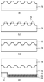
도 1은 사파이어 기판을 사용한 Ⅲ족 질화물계 화합물 반도체의 일반적인 구조를 나타낸 도면이다.1 is a view showing a general structure of a group III nitride compound semiconductor using a sapphire substrate.
도 2a 및 2b는 종래 기술에 의해 사파이어 기판 상에 Ⅲ족 질화물계 화합물 반도체를 형성시킨 것을 나타낸 도면이다. 2A and 2B show a group III nitride compound semiconductor formed on a sapphire substrate according to the prior art.
도 2c는 종래 기술에 의한 요철 구조를 지닌 기판 상에 LED를 형성시키는 과정을 개략적으로 나타낸 도면이다.2C is a view schematically illustrating a process of forming an LED on a substrate having a concave-convex structure according to the prior art.
도 3a는 본 발명에 의한 발광 소자의 기판으로 사용되는 기판을 나타낸 단면도이다. 3A is a cross-sectional view showing a substrate used as a substrate of the light emitting device according to the present invention.
도 3b는 상기 도 3a의 기판 표면을 나타낸 사시도이다.3B is a perspective view of the substrate surface of FIG. 3A.
도 3c는 본 발명에 의한 곡면형 돌출부가 형성된 기판을 포함하는 플립-칩(flip-chip) 형태의 발광 소자 단면도이다.3C is a cross-sectional view of a light emitting device having a flip-chip type including a substrate on which curved protrusions are formed according to the present invention.
도 4a 내지 도 4d는 본 발명에 의한 발광 소자의 제조 과정을 나타낸 단면도이다.4A to 4D are cross-sectional views illustrating a manufacturing process of a light emitting device according to the present invention.
도 5a는 본 발명에 의한 곡면형 돌출부 표면을 지닌 사파이어 기판 상에 GaN층을 도포하여 평탄화시키는 과정을 나타낸 SEM 사진이며, 도 5b는 종래 기술에 의한 상부가 평탄한 형태의 요철 표면을 지닌 사파이어 기판 상에 GaN층을 도포하여 평탄화하는 과정을 나타낸 SEM 사진이다.FIG. 5A is a SEM photograph illustrating a process of planarizing a GaN layer on a sapphire substrate having a curved protrusion surface according to the present invention. FIG. 5B is a sapphire substrate having a concave-convex surface having a flat upper surface according to the prior art. SEM image showing the process of applying a GaN layer to planarization.
도 6은 종래 기술 및 본 발명에 의한 발광 소자의 광출력을 비교하기 위한 도면이다.6 is a view for comparing the light output of the light emitting device according to the prior art and the present invention.
< 도면의 주요 부분에 대한 부호의 설명 > <Description of Symbols for Main Parts of Drawings>
11, 21, 31... 사파이어 기판 12, 23, 33... n-GaN층11, 21, 31 ... Sapphire
13, 22, 34... 활성층 14, 25, 35... p-GaN층13, 22, 34 ...
15, 26, 36... p형 전극층 16, 27, 37... n형 전극층15, 26, 36 ... p-
24... facet 성장하는 GaN층 32... 돌출부24 ... facet growing GaN
본 발명은 발광 소자에 관한 것으로 보다 상세하게는, 발광 소자에 사용되는 기판의 표면 결정 방위를 한정하여, 결함 밀도 제어 및 스트레스 분포의 제어가 용이하며, 광추출 효율을 향상시킨 고효율 발광 소자에 관한 것이다. The present invention relates to a light emitting device, and more particularly, to a high-efficiency light emitting device that limits the surface crystallographic orientation of a substrate used in the light emitting device, facilitates defect density control and stress distribution, and improves light extraction efficiency. will be.
일반적으로 발광 소자에는 레이저 다이오드 및 발광 다이오드가 있으며, 이중 발광 다이오드(light emitting diode:LED)는 화합물 반도체의 특성을 이용하여, 전기 에너지를 적외선, 가시광선 또는 빛의 형태로 변환시킨 신호를 발신하는데 사용되는 소자이다. 전기 에너지를 광 에너지로 변환시키는 것은 크게 온도 복사 및 발광(luminescence)의 두가지로 구별된다. 이때, 발광에는 광에 의한 여기에 따른 photo luminescence, x 선이나 전자선의 조사로 인해 발생하는 cathode luminescence 및 EL(electro luminescence) 등이 있다. 여기서 발광 다이오드는 EL의 일종이며, 현재 Ⅲ-Ⅴ족 화합물 반도체를 이용한 발광 다이오드가 실용화 되고 있다. Generally, a light emitting device includes a laser diode and a light emitting diode, and a light emitting diode (LED) uses a characteristic of a compound semiconductor to transmit a signal in which electrical energy is converted into an infrared, visible or light form. It is an element used. The conversion of electrical energy into light energy is largely divided into temperature radiation and luminescence. In this case, light emission includes photo luminescence due to excitation by light, cathode luminescence generated by irradiation of x-rays or electron beams, and electroluminescence (EL). The light emitting diode is a kind of EL, and a light emitting diode using a III-V group compound semiconductor has been put into practical use.
Ⅲ족 질화물계 화합물 반도체는 직접천이형 반도체이며, 다른 반도체를 이용한 소자보다 고온에서 안정된 동작을 얻을 수 있어서, 발광 다이오드(LED)나 레이저 다이오드(laser diode : LD) 등의 발광 소자에 널리 응용되고 있다. 이와 같은 Ⅲ족 질화물계 화합물 반도체는 통상 사파이어(sapphire : Al2O3)를 기판으로 이용하여 그 위에 형성되는 것이 일반적이다. Group III-nitride compound semiconductors are direct-transition type semiconductors, and have a stable operation at a high temperature than devices using other semiconductors, and are widely applied to light emitting devices such as light emitting diodes (LEDs) and laser diodes (LDs). have. Such a group III nitride compound semiconductor is generally formed thereon using sapphire (Al 2 O 3 ) as a substrate.
도 1에는 사파이어 기판을 사용한 Ⅲ족 질화물계 화합물 반도체의 일반적인 구조를 나타내었다. 사파이어 기판(11) 상부에 n-GaN층(12)이 형성되며, 상기 n-GaN층(12) 상부의 일부위에 활성(active)(13)층, p-GaN층(14) 및 p형 전극층(15)이 차례로 형성된다. 그리고, 상기 n-GaN(12)층 상부의 상기 활성층(13)이 형성되지 않은 부위에 n형 전극층(16)이 형성된다. 일반적인 LED에서는 내부의 활성층에서 발생된 빛을 얼마나 효율적으로 외부로 추출할 수 있는가가 중요한 문제이다. 1 shows a general structure of a group III nitride compound semiconductor using a sapphire substrate. An n-
사파이어 기판 및 활성층의 종방향으로 발생된 빛을 효율적으로 추출하기 위해 투명전극 또는 반사층을 형성하는 등을 노력을 해 왔다. 그러나, 활성층에서 발생하는 빛의 상당량은 횡방향으로 전파하게 되므로 이를 종방향으로 추출하기 위해, 예를 들어 반도체 소자의 적층 구조 측벽에 소정의 각도를 형성시키고, 상기 측벽을 반사면으로 형성시키는 등의 노력을 하였으나 그 가공 및 비용면에서 문제 점이 있다. 또한, 사파이어 기판을 사용한 Ⅲ족 질화물계 화합물 반도체 발광 소자의 광출력을 향상시키기 위해, 플립칩(flip chip) 형태의 소자 구조를 채택함에 있어서 광추출 효율은 GaN과 사파이어 기판간의 굴절율 차이에 의해 약 40% 대에 머물고 있다.Efforts have been made to form transparent electrodes or reflective layers to efficiently extract light generated in the longitudinal direction of the sapphire substrate and the active layer. However, since a considerable amount of light generated in the active layer propagates in the lateral direction, in order to extract it in the longitudinal direction, for example, a predetermined angle is formed on the sidewalls of the stacked structure of the semiconductor device, and the sidewalls are formed as the reflective surface. Has tried, but there are problems in processing and cost. In addition, in order to improve the light output of the group III nitride compound semiconductor light emitting device using the sapphire substrate, the light extraction efficiency in the case of adopting a flip chip type device structure is about due to the difference in refractive index between GaN and the sapphire substrate. 40% stay.
최근에는 도 2a에 나타낸 바와 같이, 사파이어 기판(21) 표면을 가공하여 요철 구조를 형성시키고, 그 상부에 활성층(22) 등을 포함한 반도체 결정층들을 형성시킨 LED 구조가 소개되었다. 이는 활성층(22)의 하방에 요철 모양의 굴절율 계면을 형성시킴으로써, 소자 내부에서 소멸하는 횡방향 빛의 일부를 외부로 추출 가능하도록 한 것이다. Recently, as shown in FIG. 2A, an LED structure in which a surface of the
또한, 사파이어 기판(21) 상에 Ⅲ족 질화물계 화합물 반도체를 형성시킨 경우, 사파이어 기판(21)과 Ⅲ족 질화물계 화합물 반도체와의 격자 정수의 부정합(miss fit)에 의해 전위가 발생하는 문제점이 있다. 이를 방지하기 위해, 도 2b와 같이 사파이어 기판(21) 표면에 요철 구조를 도입하여, 그 위에 GaN층(23)을 형성시켰다. 이러한 요철 구조를 지닌 사파이어 기판 상에 LED를 형성시키는 공정을 개략적으로 나타낸 것이 도 2c이다. 즉, 도 2c-(a)와 같은 요철 구조를 지닌 사파이어 기판(21)상에, GaN 층(23)을 형성시키는 경우, 도 2c-(b)와 같이 요철의 상부 및 각 요철의 측부에서 GaN이 패싯(facet)성장(24)을 하게 되고, 이러한 성장이 진행된 뒤, 도 2c-(c)와 같은 평탄화된 GaN층(23)을 얻을 수 있다. 이렇게 평탄화된 GaN층(23) 상부에 활성층(22) 등을 형성시켜, 발광 다이오드를 완성한 것을 도 2c-(d)에 나타내었다.
In addition, in the case where the group III nitride compound semiconductor is formed on the
이와 같이 패턴된 사파이어 기판(Patterned Sapphire Substrate ; PSS)을 사용하여 반도체 결정층을 성장시키는 경우, 패턴 상에서 실질적으로 패싯(facet) 성장이 이루어진 뒤에 평탄화가 진행되므로 그 평탄화를 위해 상당한 두께로 재성장을 해야하는 문제점이 있다. When the semiconductor crystal layer is grown by using a patterned sapphire substrate (PSS), the planarization is performed after the facet growth is substantially performed on the pattern. There is a problem.
또한, 사파이어 기판에 단차를 형성시키고, 상기 단차의 상면 및 측부에서 3족 질화물계 화합물 반도체를 성장시켜, 관통 전위를 방지하는 구조가 소개되었다.(WO2001-69663호) 그러나, 단차 하단에 공간(void)이 형성되고, 성장층을 평탄화시키기 위해서는 3족 질화물계 화합물 반도체를 상대적으로 두껍게 형성시켜야 하는 단점이 있다. In addition, a structure is provided in which a step is formed in the sapphire substrate, the group III-nitride compound semiconductor is grown on the upper side and the side of the step to prevent the penetration potential. (WO2001-69663) void) is formed, and in order to planarize the growth layer, a group III nitride compound semiconductor must be formed relatively thick.
그 외에 사파이어 기판상에서 반도체 결정층의 재성장시, 결함 밀도를 감소시키기 위한 방법으로 ELOG 및 PENDEO 법 등이 사용되고 있다. 그러나, ELOG의 경우 별도의 마스크 층이 필요하고, PENDEO 법의 경우 기판과의 계면 부위에 공동(void)이 형성되어 광추출 효율 측면에서 손실로 작용하는 문제점이 있다. In addition, ELOG and PENDEO methods are used as methods for reducing the defect density upon regrowth of the semiconductor crystal layer on the sapphire substrate. However, in the case of ELOG, a separate mask layer is required, and in the case of the PENDEO method, there is a problem in that a void is formed at an interface portion with the substrate, which acts as a loss in light extraction efficiency.
본 발명은 상기 문제점을 해결하기 위한 것으로, 패턴된 기판 상에 발광층을 포함하는 발광 소자를 형성시키는 경우, 그 평탄화가 효율적으로 진행되며, 반도체 결정층의 성장 및 발광 소자의 완성된 형태에서도 균일한 결합 밀도 제어 및 스트레스 분포의 제어가 용이한 기판 및 발광 소자를 제공하는 것을 목적으로 한다. 또한, 최종적으로 발광층에서 발생한 빛의 발광 소자 외부로의 추출 효율을 높일 수 있는 발광 소자를 제공하는 것을 목적으로 한다. The present invention is to solve the above problems, when forming a light emitting device including a light emitting layer on a patterned substrate, the planarization is efficiently progressed, even in the growth of the semiconductor crystal layer and the finished form of the light emitting device It is an object of the present invention to provide a substrate and a light emitting device in which bonding density control and stress distribution control are easy. In addition, an object of the present invention is to provide a light emitting device capable of increasing the extraction efficiency of light generated in the light emitting layer to the outside of the light emitting device.
상기 목적을 달성하기 위해, 본 발명에서는 기판 및 상기 기판 상에 활성층을 포함하는 반도체 결정층들이 형성된 발광 소자에 있어서, In order to achieve the above object, the present invention provides a light emitting device in which a semiconductor crystal layer including a substrate and an active layer on the substrate is formed,
상기 기판은 한개 이상의 곡면형 돌출부를 포함하며, 상기 돌출부 표면의 결정방위는 (0001)면과 상이한 반도체 결정 방위를 갖는 면으로 이루어짐으로써, 그 상부에 형성되는 Ⅲ 족 질화물계 화합물 반도체의 성장 방위와 서로 다른 것을 특징으로 하는 발광 소자를 제공한다.The substrate includes one or more curved protrusions, and the crystal orientation of the surface of the protrusions is made of a surface having a semiconductor crystal orientation different from the (0001) plane, thereby increasing the growth orientation of the group III nitride compound semiconductor formed thereon. It provides a light emitting device characterized in that the different.
본 발명에 있어서, 상기 돌출부 표면의 각 부위의 곡률은 0보다 큰며, 상기 돌출부 형태는 반구형 또는 스트라이프형이 될 수 있다.In the present invention, the curvature of each portion of the surface of the protrusion is greater than zero, the protrusion shape may be hemispherical or striped.
본 발명에 있어서, 상기 곡면형 돌출부의 각 표면은 (0001)면과 상이한 결정 방위를 가진다.In the present invention, each surface of the curved protrusion has a crystal orientation different from the (0001) plane.
본 발명에 있어서, 상기 기판은 사파이어, 또는 Si계 기판이다. In the present invention, the substrate is sapphire or Si-based substrate.
본 발명에 있어서, 상기 반도체 결정층은 Ⅲ족 질화물계 화합물 반도체이며, 그 구조는 예를 들어, n-GaN층, 상기 n-GaN층 상의 일부위에 활성층, p-GaN층 및 p형 전극층이 차례로 형성되며, 상기 n-GaN층 상부의 상기 활성층이 형성되지 않은 부위에 n형 전극층이 형성된 것이 바람직하다.In the present invention, the semiconductor crystal layer is a group III nitride compound semiconductor, and the structure thereof is, for example, an n-GaN layer, an active layer, a p-GaN layer, and a p-type electrode layer on a portion of the n-GaN layer in order. It is preferable that the n-type electrode layer is formed on a portion where the active layer is not formed on the n-GaN layer.
또한, 본 발명에서는, 기판 및 상기 기판 상에 활성층을 포함하는 반도체 결정층들이 형성된 발광 소자의 제조 방법에 있어서,In addition, in the present invention, in the method of manufacturing a light emitting device in which a semiconductor crystal layer including a substrate and an active layer on the substrate is formed,
(가) 평면형 기판 상에 한개 이상의 곡면형 돌출부를 형성시키는 단계; 및(A) forming at least one curved protrusion on the planar substrate; And
(나) 상기 기판 상에 활성층을 포함한 반도체 결정층들을 형성시키는 단계; 를 포함하는 것을 특징으로 하는 발광 소자의 제조 방법을 제공한다. (B) forming semiconductor crystal layers including an active layer on the substrate; It provides a method of manufacturing a light emitting device comprising a.
본 발명에 있어서, 상기 (가) 단계는 평면형 기판 상에 포토 레지스트를 패터닝 하는 단계; In the present invention, the step (a) comprises: patterning a photoresist on the planar substrate;
하드 베이킹을 실시하는 단계; 및 Performing hard baking; And
상기 기판면을 식각하여 한개 이상의 곡면형 돌출부를 형성시키는 단계;를 포함하는 것이 바람직하다. And etching the substrate surface to form at least one curved protrusion.
본 발명에 있어서, 상기 기판면을 식각하는 경우, 식각 가스는 Cl2, BCl3, HCl, CCl4, SiCl4 등의 Cl 계열의 가스 중에서 선택될 수 있다. In the present invention, when etching the substrate surface, the etching gas may be selected from Cl-based gas, such as Cl 2 , BCl 3 , HCl, CCl 4 , SiCl 4 .
또한, 본 발명에서는, 기판 및 상기 기판 상에 활성층을 포함하는 반도체 결정층들이 형성된 발광 소자의 제조 방법에 있어서,In addition, in the present invention, in the method of manufacturing a light emitting device in which a semiconductor crystal layer including a substrate and an active layer on the substrate is formed,
(가) 상기 기판 표면에 한개 이상의 곡면형 돌출부를 형성시키는 단계; 및 (A) forming at least one curved protrusion on the surface of the substrate; And
(나) 상기 곡면형 돌출부 사이의 기판 평탄면으로 부터 Ⅲ족 질화물계 화합물 반도체 결정층을 성장시키기 시작하여, 상기 곡면형 돌출부 표면을 덮도록 성장시키는 단계;를 포함하는 발광 소자의 제조 방법을 제공한다. (B) starting to grow a group III nitride compound semiconductor crystal layer from the planar flat surface between the curved protrusions, and growing to cover the surface of the curved protrusions; do.
이하, 도면을 참조하여 본 발명에 의한 발광 소자에 대해 상세히 설명하고자 한다. Hereinafter, a light emitting device according to the present invention will be described in detail with reference to the accompanying drawings.
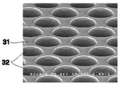
도 3a는 본 발명에 의한 발광 소자의 기판으로 사용되는 사파이어 기판 또는 Si를 포함하는 기판의 단면도이다. 도 3a에 나타낸 바와 같이 본 발명에 의한 발광 소자의 기판(31) 표면에는 둥근 형상을 지닌 돌출부(32)들이 형성되어 있다. 이러 한 돌출부(32)는 종래 기술에 관한 도 2a 및 도 2b의 요철 구조를 지닌 기판의 형상과는 다르다. 즉, 도 2a 및 도 2b의 요철 구조는 그 상단부 및 측부가 각각 평면 형태로 상단부 및 측부가 구별되며, 상기 측부는 기판(21)면을 기준으로 소정 각도로 기울어진 형태를 나타낸다. 3A is a cross-sectional view of a sapphire substrate or a substrate including Si used as a substrate of the light emitting device according to the present invention. As shown in FIG. 3A, protruding
그러나, 본 발명에 관한 도 3a의 기판(31) 표면에 형성된 돌출부(32)는 돌출부(32) 전체가 곡면을 이루고 있어, 상단부 및 측부의 구별이 없으며, 평탄면이 존재하지 않는 곡면형인 것을 특징으로 한다. 따라서, 돌출부(32)의 각 부위에서의 곡률은 0보다 크다. 상기 돌출부(32) 및 상기 기판(31) 사이를 제외하고는 모서리부가 존재하지 않는다. 그리하여, 본 발명에 의한 발광 소자의 기판(31)의 돌출부(32) 표면의 결정 방위는 그 상부에 형성될 Ⅲ족 질화물계 화합물 반도체의 결정 성장 방위(c축)과 다르다. 즉, 본 발명에 의한 곡면형 돌출부(32) 표면은 (0001)면과 상이한 결정 성장면으로 이루어진다. 따라서, 상기 돌출부(32) 표면에서는 상기 Ⅲ족 질화물계 화합물 반도체의 성장이 잘 일어나지 않는다.However, since the
도 3b는 상기 도 3a의 기판(31) 표면을 나타낸 사시도이다. 돌출부(32)는 구의 일부를 절단한 형태로 기판 표면에 존재하는 모든 돌출부(32)가 동일한 크기, 형태가 될 수 있으며, 이에 한정되지 아니하며, 돌출부(32)의 크기, 형태 및 돌출부들의 각 부위에서의 곡률은 조금씩 차이가 생길 수 있다. 예를 들어, 돌출부(32) 하부 쪽의 곡률이 상부쪽의 곡률보다 클 수도 있고, 그 반대가 될 수도 있다. 또한, 그 돌출부(32)의 형태는 전체가 곡면을 가지면서, 반구형, 스트라이프(stripe)형 또는 구부러진 말굽형태도 될 수 있다. 그리고, 돌출부의 배열 형태에도 제한이 없으며, 격자형 배열 구조와 같이 규칙적인 형태가 될 수 있으며, 또한 불규칙적인 배열 형태를 지닐 수도 있다. FIG. 3B is a perspective view illustrating the surface of the
본 발명에 의한 발광 소자의 기판(31)은 사파이어 기판에 한정되지 아니하며, 실리콘(Si), 탄화 규소(SiC)등 Ⅲ족 질화물계 화합물 반도체를 성장시키는 기판이면 사용될 수 있다. The
도 3c는 본 발명에 의한 다수의 곡면형 돌출부(32)가 형성된 기판(31)을 포함하는 플립-칩(flip-chip) 형태의 발광 소자 단면도이다. 도면을 참고하면, 다수의 곡면형 돌출부(32)가 형성된 기판(31) 상에 n-GaN층(33)이 형성되며, 상기 n-GaN층(33) 상의 일부위에 활성(active)층(34), p-GaN층(35) 및 p형 전극층(36)이 차례로 형성된다. 그리고, 상기 n-GaN층(33) 상부의 상기 활성층(34)이 형성되지 않은 부위에 n형 전극층(37)이 형성된다. 상기 기판(31)을 제외한 구조는 Ⅲ족 질화물계 화합물 반도체 발광 소자와 크게 다르지 않다. 이때, 상기 기판(31) 상에 형성시키는 Ⅲ족 질화물계 화합물 반도체는 GaN에 한정되지 아니하며, AlN 또는 InN과 같은 2원계, 기타 3원계 및 4원계를 포함한다.3C is a cross-sectional view of a light emitting device in a flip-chip form including a
이하, 본 발명에 의한 발광 소자의 제조 방법에 대해 설명하기로 한다. 기판 표면에 다수의 곡면형 돌출부를 형성시키는 공정의 일 실시예를 설명하면 다음과 같다. Hereinafter, the manufacturing method of the light emitting element by this invention is demonstrated. An embodiment of a process of forming a plurality of curved protrusions on a substrate surface is described below.
먼저, 평면형 기판 상에 포토 레지스트(photo resist:PR)를 패터닝(patterning) 한다. 여기서는 일반적인 사진 식각(photolithography) 방법으로 진행하며, 기판의 에칭 깊이에 대한 목표값에 따라 사용되는 포토 레지스트의 두께가 달라진다. 예를 들어, 사파이의 기판의 식각 깊이가 약 1.2㎛인 경우, 포토 레지스트의 두께는 약 2㎛ 정도로 할 수 있다. First, a photo resist (PR) is patterned on a planar substrate. In this case, the photolithography method is used, and the thickness of the photoresist used varies depending on the target value for the etching depth of the substrate. For example, when the etching depth of the sapphire substrate is about 1.2 mu m, the thickness of the photoresist may be about 2 mu m.
다음으로, 하드 베이킹(hard baking)을 실시한다. 이때의 온도는 섭씨 약 110도 내외로 한다. Next, hard baking is performed. The temperature at this time is about 110 degrees Celsius.
그리고, 상기 사파이어 기판을 식각하게 되는데, 이때에는 일반적인 RIE(Reactive Ion Etching : 반응성 이온 식각)법으로 한다. 본 발명과 같은 곡면형의 돌출부를 기판 상에 형성시키기 위해서 식각 가스, 작동 압력 및 작동 파워 등을 적절히 조절한다. 본 실험에서는 식각 가스로 Cl2/BCl3를 사용했고, 작동 압력은 3mTorr, 작동 파워는 800W를 사용했으나, 이에 한정되지 않는다. 예를 들어, 사용되는 식각 가스로는 Cl2, BCl3, HCl, CCl4, SiCl4 등의 Cl 계열의 가스 중에서 선택하는 것이 바람직하다. 그리고, 작동 압력도 사용되는 식각 가스에 따라 수 mTorr ~ 수십 mTorr 사이에서 조절할 수 있으며, 1 ~ 40 mTorr 정도면 바람직하다. In addition, the sapphire substrate is etched. In this case, a general reactive ion etching (RIE) method is used. In order to form a curved protrusion like the present invention on a substrate, an etching gas, an operating pressure, an operating power, and the like are appropriately adjusted. In this experiment, Cl 2 / BCl 3 was used as an etching gas, an operating pressure of 3 mTorr, and an operating power of 800 W, but the present invention is not limited thereto. For example, the etching gas used may be selected from a Cl series gas such as Cl 2 , BCl 3 , HCl, CCl 4 , and SiCl 4 . In addition, the operating pressure can also be adjusted between a few mTorr ~ several tens mTorr depending on the etching gas used, 1 ~ 40 mTorr is preferred.
상기와 같은 공정에 의해 기판 표면에 다수의 곡면형 돌출부를 형성시킬 수 있다. 그런 다음 상기 기판 상부에 발광 소자 제작에 필요한 n-GaN층, 활성층, p-GaN층, p형 전극층 및 n형 전극층 등을 형성시킨다. 본 발명에 의한 발광 소자에 있어서, 기판(31) 상부에 형성되는 화합물 반도체층 들은 종래의 형태와 크게 다르지 않으며, 그 제조 공정도 공지 기술을 사용하면 용이하게 실시할 수 있다. 다만, 상기 곡면형 돌출부를 지닌 기판 표면에 발광 소자의 구조를 형성시키는 경우, 별도의 마스크 층이 필요 없다.
By the above process, a plurality of curved protrusions can be formed on the surface of the substrate. Then, an n-GaN layer, an active layer, a p-GaN layer, a p-type electrode layer, an n-type electrode layer, and the like, which are necessary for manufacturing a light emitting device, are formed on the substrate. In the light emitting device according to the present invention, the compound semiconductor layers formed on the
이러한 제조 공정을 도 4a내지 도 4d에서 개략적으로 나타내었다. 도 4a 내지 도 4d는 본 발명에 의한 발광 소자의 제조 과정을 나타낸 단면도이다. 즉, 도 4a 및 도 4b는 평면 기판(31) 표면을 식각하여, 곡면형 돌출부(32)를 지닌 사파이어 기판(31)을 형성시키는 것을 나타내었고, 도 4c는 상기 곡면형 돌출부(32)를 지닌 기판 상에 GaN층(33)의 초기 성장 형태를 나타낸 도면이다. 그리고, 도 4d는 상기 도 4c의 GaN층(33)을 계속 성장시켜, 그 표면을 평탄화시킨 것을 나타낸 도면이다. 도 4c의 평탄화된 n-GaN층(33) 상부에 기타 활성층(34) 및 전극층들(36, 37)을 모두 형성시켜 완성된 플립-칩 형태의 발광 소자가 바로 도 3c에 나타낸 것이다. 곡면형 돌출부(32)를 지닌 기판(31) 및 GaN 계면 상에 공동이 형성되지 않는다. 상기 GaN층(33) 이후의 활성층 등의 성장 공정은 종래 기술에 잘 나타나 있음으로 여기서는 생략한다. This manufacturing process is schematically illustrated in FIGS. 4A-4D. 4A to 4D are cross-sectional views illustrating a manufacturing process of a light emitting device according to the present invention. 4A and 4B illustrate etching the surface of the
도 4a 내지 도 4d에 도시된 발광 소자 형성 형태는 상기 도 2c에 나타낸 요철 형태의 표면을 지닌 기판 상에 발광 소자를 형성시킨 것과 차이가 있음을 알 수 있다. 즉, 본 발명에 의한 발광 소자에서 GaN 평탄화층(32)을 얻는 경우, 상기 GaN이 종래 기술과 같은 패싯(facet) 성장을 하지 않으며, 평탄화 막을 얻기 위한 GaN층(32)의 두께가 상대적으로 얇게 된다. 그리고, 에피탁샬 성장이 일어나지만, 본 발명의 경우 돌출부(32) 표면에서는 GaN층(33) 성장이 잘 일어나지 않는다. It can be seen that the light emitting device formation form shown in FIGS. 4A to 4D differs from the light emitting device formation on the substrate having the uneven surface shown in FIG. 2C. That is, when the
본 발명의 경우, 돌출부(32)의 표면이 그 상부에 형성되는 Ⅲ족 질화물계 화합물 반도체의 결정 성장 방향과 다른 결정 방위를 가지도록 하기 위해 곡면형 돌출부(32)를 형성시킨 것이다. 따라서, Ⅲ족 질화물계 화합물 반도체의 성장은 돌출 부(32)들 사이의 기판(31) 표면, 즉 평탄부에서 시작하고, 그 두께가 두꺼워지면서, 상기 돌출부(32)의 측부 및 최상부를 덮게되는 것이다.In the present invention, the
이를 도 5a 및 도 5b의 SEM 사진을 통해 확인하였다. 도 5a는 본 발명의 일 실시예에 의한 곡면형 돌출부(2) 표면을 지닌 기판(31) 상에 GaN층(33)을 도포하여 평탄화하는 과정을 나타낸 것이고, 도 5b는 종래 기술에 의한 요철 표면을 지닌 기판(31) 상에 GaN층(33)을 도포하여 평탄화하는 과정을 나타낸 것이다. 배율이 틀리지만, 기판(31)표면에 형성된 곡면형 돌출부(32) 및 평탄면을 지닌 요철은 모두 그 높이가 같은 상태로 제작되었다. 같은 조건에서 두개의 기판(31) 상에 GaN층(33)을 형성시키면서 SEM 사진을 촬영한 결과를 살펴보면, 도 5a-(b) 및 도 5b-(b)에서 본 발명과 종래 기술이 명확한 차이가 나타남을 알 수 있다. This was confirmed through the SEM pictures of FIGS. 5A and 5B. 5A illustrates a process of applying and planarizing a
즉, 도 5a-(b)의 경우, 곡면형 돌출부(32)의 상단부를 제외하고는 GaN층(33)에 의해 기판(31)의 평탄화가 진행되었다. 이에 반해, 도 5b-(b)의 경우, 요철부의 상부 및 그 측면에서 GaN이 패싯 성장이 일어나고 있으며, 평탄화 정도도 매우 낮은 상태이다. 또한, 도 5a-(c)의 본 발명의 경우, 곡형 돌출부(32)를 지닌 기판(31) 상부에 GaN이 도포되면서 완전한 평탄화가 이루어졌다. 그러나, 도 5b-(c)의 경우 요철의 상단부는 평탄화가 이루어졌으나, 각 요철 사이에는 완전한 평탄화가 이루어지지 않은 상태임을 알 수 있다. That is, in the case of FIGS. 5A-B, planarization of the
도 6은 종래 기술 및 본 발명에 의한 발광 소자의 광출력을 비교하기 위한 도면이다. 여기서, A는 종래의 평면 형태의 기판(11) 상에 형성시킨 발광 소자를 나타내며, 상기 도 1의 구조에 해당한다. B는 종래의 요철 형태의 표면을 지닌 기 판(21) 상에 형성시킨 발광 소자의 구조를 나타내며, 상기 도 2d에 해당한다. 그리고, C는 본 발명에 의한 곡면형 돌출부(32)를 지닌 기판(31) 상에 형성시킨 발광 소자를 나타내며, 상기 도 3c에 해당한다.6 is a view for comparing the light output of the light emitting device according to the prior art and the present invention. Here, A represents a light emitting device formed on a conventional
도 6을 참조하면, 평면 구조의 기판(11) 상에 발광 소자를 형성시킨 A의 경우에 비해, 요철 표면을 지닌 기판(21) 상에 발광 소자를 형성시킨 B가 광출력이 약 50% 향상되었고, 곡면형 돌출부(32) 표면을 지닌 기판(31) 상에 발광 소자를 형성시킨 C가 A에 비해 광출력이 약 60%이상 향상되었음을 알 수 있다. 또한, 본 발명에 의한 발광 소자 C가 요철 표면의 기판(21) 상에 발광 소자를 형성시킨 B에 비해 광출력이 약 10%이상 향상되었음을 알 수 있다. 이는 곡면형 돌출부(32)를 지닌 기판(31)을 사용함으로써 반도체 결정층 사이의 계면 형태가 광경로를 변경시키는 Optical lens를 형성하고, 성장하는 반도체 결정층의 결함 밀도를 감소시켰기 때문이다.Referring to FIG. 6, compared to the case of A in which a light emitting device is formed on a
상기한 설명에서 많은 사항이 구체적으로 기재되어 있으나, 그들은 발명의 범위를 한정하는 것이라기보다, 바람직한 실시예의 예시로서 해석되어야 한다. 본 발명의 범위는 설명된 실시예에 의하여 정하여 질 것이 아니고 특허 청구범위에 기재된 기술적 사상에 의해 정하여져야 한다. 예를 들어, 본 발명에 의한 발광 소자의 곡면형 돌출부는 그 상부에 형성될 Ⅲ족 질화물계 화합물 반도체의 결정 성장 방향과 다르면 되며, 그 형상이 반구형, 스트라이프형, 말굽형 등이 될 수 있고, 배열 형태도 규칙적, 불규칙적인 배열 형태가 모두 포함될 수 있다. While many details are set forth in the foregoing description, they should be construed as illustrative of preferred embodiments, rather than to limit the scope of the invention. The scope of the invention should not be defined by the described embodiments, but should be determined by the technical spirit described in the claims. For example, the curved protrusion of the light emitting device according to the present invention may be different from the crystal growth direction of the group III nitride compound semiconductor to be formed thereon, and the shape may be hemispherical, striped, horseshoe, or the like. The array form may include both regular and irregular array forms.
본 발명에 의하면, 곡면형 돌출부를 지니도록 패턴된 기판 상에 발광층을 포함하는 발광 소자를 형성시키는 경우, 그 평탄화가 효율적으로 진행되며, 반도체 결정층의 성장 및 발광 소자의 완성된 형태에서도 균일한 결함 밀도 제어 및 스트레스 분포의 제어가 용이하며, 결과적으로 발광층에서 발생한 빛의 발광 소자 외부로의 추출 효율을 높일 수 있다. According to the present invention, when a light emitting device including a light emitting layer is formed on a substrate patterned to have a curved protrusion, the planarization can be efficiently carried out, and the growth of the semiconductor crystal layer and the finished form of the light emitting device are uniform. It is easy to control the defect density and control the stress distribution, and as a result, the extraction efficiency of light generated in the light emitting layer to the outside of the light emitting device can be improved.
Claims (13)
Priority Applications (7)
| Application Number | Priority Date | Filing Date | Title |
|---|---|---|---|
| KR1020030073442A KR100714639B1 (en) | 2003-10-21 | 2003-10-21 | Light emitting element |
| US10/852,249 US20050082546A1 (en) | 2003-10-21 | 2004-05-25 | Light-emitting device and method of manufacturing the same |
| CN2009101785272A CN101667617B (en) | 2003-10-21 | 2004-06-10 | Light emitting device and manufacturing method thereof |
| CN2004100484504A CN1610135B (en) | 2003-10-21 | 2004-06-10 | Method for manufacturing light emitting device |
| JP2004212028A JP4580193B2 (en) | 2003-10-21 | 2004-07-20 | Light emitting element |
| US11/450,389 US7759140B2 (en) | 2003-10-21 | 2006-06-12 | Light-emitting device and method of manufacturing the same |
| JP2010105599A JP5666164B2 (en) | 2003-10-21 | 2010-04-30 | Method for manufacturing light emitting device |
Applications Claiming Priority (1)
| Application Number | Priority Date | Filing Date | Title |
|---|---|---|---|
| KR1020030073442A KR100714639B1 (en) | 2003-10-21 | 2003-10-21 | Light emitting element |
Publications (2)
| Publication Number | Publication Date |
|---|---|
| KR20050038207A KR20050038207A (en) | 2005-04-27 |
| KR100714639B1 true KR100714639B1 (en) | 2007-05-07 |
Family
ID=34510986
Family Applications (1)
| Application Number | Title | Priority Date | Filing Date |
|---|---|---|---|
| KR1020030073442A Expired - Fee Related KR100714639B1 (en) | 2003-10-21 | 2003-10-21 | Light emitting element |
Country Status (4)
| Country | Link |
|---|---|
| US (2) | US20050082546A1 (en) |
| JP (2) | JP4580193B2 (en) |
| KR (1) | KR100714639B1 (en) |
| CN (2) | CN1610135B (en) |
Cited By (2)
| Publication number | Priority date | Publication date | Assignee | Title |
|---|---|---|---|---|
| KR101055266B1 (en) | 2009-05-07 | 2011-08-09 | (주)더리즈 | Substrate for semiconductor device and semiconductor device using same |
| US8110844B2 (en) | 2010-02-10 | 2012-02-07 | Theleds Co., Ltd. | Semiconductor substrate and light emitting device using the same |
Families Citing this family (469)
| Publication number | Priority date | Publication date | Assignee | Title |
|---|---|---|---|---|
| KR100499129B1 (en) | 2002-09-02 | 2005-07-04 | 삼성전기주식회사 | Light emitting laser diode and fabricatin method thereof |
| DE102004034166B4 (en) * | 2003-07-17 | 2015-08-20 | Toyoda Gosei Co., Ltd. | Light-emitting device |
| KR100587020B1 (en) | 2004-09-01 | 2006-06-08 | 삼성전기주식회사 | High power light emitting diode package |
| US8174037B2 (en) * | 2004-09-22 | 2012-05-08 | Cree, Inc. | High efficiency group III nitride LED with lenticular surface |
| FI118196B (en) * | 2005-07-01 | 2007-08-15 | Optogan Oy | Semiconductor structure and method for producing a semiconductor structure |
| JP5082278B2 (en) * | 2005-05-16 | 2012-11-28 | ソニー株式会社 | Light emitting diode manufacturing method, integrated light emitting diode manufacturing method, and nitride III-V compound semiconductor growth method |
| JP2007019318A (en) * | 2005-07-08 | 2007-01-25 | Sumitomo Chemical Co Ltd | Semiconductor light emitting device, method for manufacturing semiconductor light emitting device substrate, and method for manufacturing semiconductor light emitting device |
| KR100958590B1 (en) | 2005-08-19 | 2010-05-18 | 한빔 주식회사 | Light emitting diode device with improved light extraction efficiency and manufacturing method thereof |
| US20070018186A1 (en) * | 2005-07-19 | 2007-01-25 | Lg Chem, Ltd. | Light emitting diode device having advanced light extraction efficiency and preparation method thereof |
| KR100610639B1 (en) * | 2005-07-22 | 2006-08-09 | 삼성전기주식회사 | Vertical structure gallium nitride-based light emitting diode device and method of manufacturing the same |
| TWI253771B (en) * | 2005-07-25 | 2006-04-21 | Formosa Epitaxy Inc | Light emitting diode structure |
| KR20070012930A (en) * | 2005-07-25 | 2007-01-30 | 엘지이노텍 주식회사 | Semiconductor light emitting device and manufacturing method thereof |
| KR20080081907A (en) * | 2005-11-03 | 2008-09-10 | 오르소소프트 인코포레이티드 | Computer Supported Surgical Multifaced Tracker Device |
| KR20070063731A (en) * | 2005-12-15 | 2007-06-20 | 엘지전자 주식회사 | Method for manufacturing a substrate on which a nano-pattern is formed and a light emitting device using the substrate |
| US20070176160A1 (en) * | 2006-01-27 | 2007-08-02 | Hamamatsu Photonics K.K. | Electron tube |
| KR101163788B1 (en) | 2006-03-05 | 2012-07-09 | 엘지이노텍 주식회사 | Nitride semiconductor light-emitting device and method thereof |
| KR100764386B1 (en) | 2006-03-20 | 2007-10-08 | 삼성전기주식회사 | Insulation structure suitable for high temperature process and its manufacturing method |
| KR100786777B1 (en) * | 2006-03-28 | 2007-12-18 | 전북대학교산학협력단 | Method of manufacturing a semiconductor structure |
| JP4637781B2 (en) * | 2006-03-31 | 2011-02-23 | 昭和電工株式会社 | GaN-based semiconductor light emitting device manufacturing method |
| KR100828873B1 (en) * | 2006-04-25 | 2008-05-09 | 엘지이노텍 주식회사 | Nitride semiconductor light emitting device and manufacturing method |
| KR100730755B1 (en) * | 2006-05-12 | 2007-06-21 | 서울옵토디바이스주식회사 | Vertical light emitting device manufacturing method and vertical light emitting device |
| KR100780233B1 (en) * | 2006-05-15 | 2007-11-27 | 삼성전기주식회사 | Semiconductor light emitting device with multi pattern structure |
| US20100273331A1 (en) * | 2006-07-05 | 2010-10-28 | National Central University | Method of fabricating a nano/micro structure |
| US20080008964A1 (en) * | 2006-07-05 | 2008-01-10 | Chia-Hua Chan | Light emitting diode and method of fabricating a nano/micro structure |
| DE102006043400A1 (en) * | 2006-09-15 | 2008-03-27 | Osram Opto Semiconductors Gmbh | Optoelectronic semiconductor chip |
| JP4228012B2 (en) | 2006-12-20 | 2009-02-25 | Necライティング株式会社 | Red light emitting nitride phosphor and white light emitting device using the same |
| JP5082752B2 (en) * | 2006-12-21 | 2012-11-28 | 日亜化学工業株式会社 | Manufacturing method of substrate for semiconductor light emitting device and semiconductor light emitting device using the same |
| WO2008081717A1 (en) * | 2006-12-22 | 2008-07-10 | Showa Denko K.K. | Method for producing group iii nitride semiconductor layer, group iii nitride semiconductor light-emitting device, and lamp |
| US7663148B2 (en) * | 2006-12-22 | 2010-02-16 | Philips Lumileds Lighting Company, Llc | III-nitride light emitting device with reduced strain light emitting layer |
| JP4908381B2 (en) | 2006-12-22 | 2012-04-04 | 昭和電工株式会社 | Group III nitride semiconductor layer manufacturing method, group III nitride semiconductor light emitting device, and lamp |
| KR101305786B1 (en) * | 2007-06-21 | 2013-09-06 | 엘지이노텍 주식회사 | Semiconductor light-emitting device and manufacturing method thereof |
| KR100916375B1 (en) | 2007-06-27 | 2009-09-07 | 주식회사 에피밸리 | Method of manufacturing semiconductor light emitting device and semiconductor light emitting device |
| WO2009002129A2 (en) * | 2007-06-27 | 2008-12-31 | Epivalley Co., Ltd. | Semiconductor light emitting device and method of manufacturing the same |
| US7905618B2 (en) | 2007-07-19 | 2011-03-15 | Samsung Led Co., Ltd. | Backlight unit |
| JP2009038377A (en) * | 2007-07-31 | 2009-02-19 | Epivalley Co Ltd | Group III nitride semiconductor light emitting device |
| KR100891761B1 (en) | 2007-10-19 | 2009-04-07 | 삼성전기주식회사 | Semiconductor light emitting device, manufacturing method thereof and semiconductor light emitting device package using same |
| JP2009295753A (en) | 2008-06-04 | 2009-12-17 | Showa Denko Kk | Method of manufacturing group iii nitride semiconductor light-emitting device and group iii nitride semiconductor light-emitting device, and lamp |
| TWI413279B (en) | 2008-06-20 | 2013-10-21 | 豐田合成股份有限公司 | Group III nitride semiconductor light-emitting device, method of manufacturing the same, and lamp |
| US9022632B2 (en) | 2008-07-03 | 2015-05-05 | Samsung Electronics Co., Ltd. | LED package and a backlight unit unit comprising said LED package |
| EP2312658B1 (en) | 2008-07-03 | 2018-06-27 | Samsung Electronics Co., Ltd. | A wavelength-converting light emitting diode (led) chip and method for fabrication of an led device equipped with this chip |
| KR101533296B1 (en) | 2008-07-08 | 2015-07-02 | 삼성전자주식회사 | NITRIDE SEMICONDUCTOR LIGHT EMITTING DEVICE HAVING PATTERN FORMED SUBSTRATE |
| TW201003980A (en) * | 2008-07-14 | 2010-01-16 | Huga Optotech Inc | Substrate for making light emitting element and light emitting element using the same |
| KR100882240B1 (en) * | 2008-09-11 | 2009-02-25 | (주)플러스텍 | Nitride semiconductor light emitting device and manufacturing method |
| JP2010092936A (en) * | 2008-10-03 | 2010-04-22 | Yamaguchi Univ | Semiconductor device |
| KR101009651B1 (en) * | 2008-10-15 | 2011-01-19 | 박은현 | Group III nitride semiconductor light emitting device |
| US8008683B2 (en) | 2008-10-22 | 2011-08-30 | Samsung Led Co., Ltd. | Semiconductor light emitting device |
| DE102008056175A1 (en) * | 2008-11-06 | 2010-05-12 | Osram Opto Semiconductors Gmbh | A method of manufacturing a radiation emitting thin film device and radiation emitting thin film device |
| WO2010056083A2 (en) | 2008-11-14 | 2010-05-20 | 삼성엘이디 주식회사 | Vertical/horizontal light-emitting diode for semiconductor |
| KR101141269B1 (en) * | 2008-12-26 | 2012-05-04 | 한국광기술원 | Light emitting diode and method of manufacturing the same |
| WO2010101348A1 (en) * | 2009-03-05 | 2010-09-10 | 우리엘에스티 주식회사 | Group 3 nitride semiconductor light-emitting device and manufacturing method thereof |
| CN102405537B (en) * | 2009-04-24 | 2014-07-30 | 财团法人首尔大学校产学协力团 | Method of fabricating substrate where patterns are formed |
| TWI387004B (en) * | 2009-04-24 | 2013-02-21 | 首爾大學校 產學協力團 | Method of manufacturing patterned substrate |
| JP2011009382A (en) * | 2009-06-24 | 2011-01-13 | Rohm Co Ltd | Semiconductor light emitting element |
| KR20110018563A (en) * | 2009-08-18 | 2011-02-24 | 우리엘에스티 주식회사 | Group III nitride semiconductor light emitting device and method of manufacturing the same |
| DE112010003358T5 (en) * | 2009-08-21 | 2012-08-02 | Soraa, Inc. | METHOD AND STRUCTURES FOR THE FAST SEPARATION OF ULTRA-TALL EPITACTIC GALLIUM AND NITROGEN-CONTAINING STRUCTURES FOR COMPONENTS |
| KR101650840B1 (en) | 2009-08-26 | 2016-08-24 | 삼성전자주식회사 | Light emitting device and method of manufacturing the same |
| JP2011129718A (en) | 2009-12-17 | 2011-06-30 | Showa Denko Kk | Substrate, template substrate, semiconductor light emitting element, semiconductor light emitting element producing method, illumination device using semiconductor light emitting element, and electronic device |
| JP5463901B2 (en) * | 2009-12-24 | 2014-04-09 | 日亜化学工業株式会社 | Light emitting device |
| KR101658838B1 (en) * | 2010-02-04 | 2016-10-04 | 엘지이노텍 주식회사 | Light emitting device and method for fabricating the same |
| US8258531B2 (en) * | 2010-03-26 | 2012-09-04 | Huga Optotech Inc. | Semiconductor devices |
| KR101252032B1 (en) | 2010-07-08 | 2013-04-10 | 삼성전자주식회사 | Semiconductor light emitting device and method of manufacturing the same |
| KR101313262B1 (en) | 2010-07-12 | 2013-09-30 | 삼성전자주식회사 | Chemical Vapor Deposition Apparatus and Method of Forming Semiconductor Thin Film Using The Same |
| KR101692410B1 (en) | 2010-07-26 | 2017-01-03 | 삼성전자 주식회사 | Light emitting device and method of manufacturing the same |
| DE112011102800T8 (en) | 2010-08-25 | 2013-08-14 | Samsung Electronics Co., Ltd. | Phosphor film, method for producing the same, coating method for a phosphor layer, method of manufacturing an LED package and LED package manufactured thereby |
| KR101710159B1 (en) | 2010-09-14 | 2017-03-08 | 삼성전자주식회사 | Group III nitride nanorod light emitting device and Manufacturing method for the same |
| KR20120027987A (en) | 2010-09-14 | 2012-03-22 | 삼성엘이디 주식회사 | Gallium nitride based semiconductor device and method of manufacturing the same |
| CN102420281B (en) * | 2010-09-28 | 2014-12-10 | 晶元光电股份有限公司 | Photoelectric element and manufacturing method thereof |
| KR20120032329A (en) | 2010-09-28 | 2012-04-05 | 삼성전자주식회사 | Semiconductor device |
| KR20120042500A (en) | 2010-10-25 | 2012-05-03 | 삼성엘이디 주식회사 | Semiconductor light emitting diode |
| KR20120050282A (en) | 2010-11-10 | 2012-05-18 | 삼성엘이디 주식회사 | Light emitting device package and method of manufacturing the same |
| KR101182584B1 (en) * | 2010-11-16 | 2012-09-18 | 삼성전자주식회사 | Manufacturing appratus and manufacturing method of led package |
| KR101591991B1 (en) | 2010-12-02 | 2016-02-05 | 삼성전자주식회사 | Light emitting device package and method thereof |
| KR20120067153A (en) | 2010-12-15 | 2012-06-25 | 삼성엘이디 주식회사 | Light emitting device, light emitting device package, manufacturing method of light emitting device, and packaging method of light emitting device |
| KR101748334B1 (en) | 2011-01-17 | 2017-06-16 | 삼성전자 주식회사 | Apparatus and method of fabricating white light emitting device |
| CN102623600A (en) * | 2011-01-31 | 2012-08-01 | 隆达电子股份有限公司 | semiconductor light emitting structure |
| EP2503606B1 (en) | 2011-03-25 | 2020-02-26 | Samsung Electronics Co., Ltd. | Light Emitting Diode, Manufacturing Method Thereof, Light Emitting Diode Module, and Manufacturing Method Thereof |
| US9236530B2 (en) | 2011-04-01 | 2016-01-12 | Soraa, Inc. | Miscut bulk substrates |
| TWI470829B (en) * | 2011-04-27 | 2015-01-21 | Sino American Silicon Prod Inc | Method for manufacturing epitaxial substrate, light emitting diode, and manufacturing method thereof |
| KR101798884B1 (en) | 2011-05-18 | 2017-11-17 | 삼성전자주식회사 | Light emitting device assembly and head light including the same |
| EP2732478B1 (en) * | 2011-07-15 | 2018-09-19 | Lumileds Holding B.V. | Method of bonding a semiconductor device to a support substrate |
| CN103078040B (en) | 2011-08-22 | 2016-12-21 | Lg伊诺特有限公司 | Light emitting device package and light device |
| US9646827B1 (en) | 2011-08-23 | 2017-05-09 | Soraa, Inc. | Method for smoothing surface of a substrate containing gallium and nitrogen |
| JP5914807B2 (en) * | 2011-12-14 | 2016-05-11 | パナソニックIpマネジメント株式会社 | Etching method for sapphire substrate |
| WO2013089521A1 (en) | 2011-12-16 | 2013-06-20 | 삼성전자주식회사 | Heat-dissipating structure for lighting apparatus and lighting apparatus |
| US8748847B2 (en) | 2011-12-23 | 2014-06-10 | Samsung Electronics Co., Ltd. | Method of manufacturing white light emitting device (LED) and apparatus measuring phosphor film |
| JP5673581B2 (en) | 2012-02-24 | 2015-02-18 | 豊田合成株式会社 | Group III nitride semiconductor light emitting device manufacturing method, group III nitride semiconductor light emitting device, lamp, and reticle |
| KR101903361B1 (en) | 2012-03-07 | 2018-10-04 | 삼성전자주식회사 | Nitride semiconductor light emitting device and manufacturing method thereof |
| KR20130109319A (en) | 2012-03-27 | 2013-10-08 | 삼성전자주식회사 | Semiconductor light emitting device, light emitting module and lighting device |
| KR101891257B1 (en) | 2012-04-02 | 2018-08-24 | 삼성전자주식회사 | Light Emitting Device and Manufacturing Method thereof |
| KR101907390B1 (en) | 2012-04-23 | 2018-10-12 | 삼성전자주식회사 | White light emitting device and display apparatus |
| KR101891777B1 (en) | 2012-06-25 | 2018-08-24 | 삼성전자주식회사 | Light emitting device having dielectric reflector and method of manufacturing the same |
| KR101978968B1 (en) | 2012-08-14 | 2019-05-16 | 삼성전자주식회사 | Semiconductor light emitting device and light emitting apparatus |
| KR101982626B1 (en) | 2012-10-17 | 2019-05-27 | 엘지이노텍 주식회사 | Light emitting device and lighting device having the same |
| KR101898680B1 (en) | 2012-11-05 | 2018-09-13 | 삼성전자주식회사 | Nano-structured light emitting device |
| KR101898679B1 (en) | 2012-12-14 | 2018-10-04 | 삼성전자주식회사 | Nano-structured light emitting devices |
| KR101967836B1 (en) | 2012-12-14 | 2019-04-10 | 삼성전자주식회사 | 3-Dimesional Light Emitting device and fabrication thereof |
| CN103035802A (en) * | 2012-12-15 | 2013-04-10 | 华南理工大学 | Patterned substrate and light emitting diode (LED) chip used for LED inverted-assembly structure |
| KR102011101B1 (en) | 2012-12-26 | 2019-08-14 | 삼성전자주식회사 | Light emitting device package |
| KR102018615B1 (en) | 2013-01-18 | 2019-09-05 | 삼성전자주식회사 | Semiconductor light emitting device and manufacturing method of the same |
| KR102022266B1 (en) | 2013-01-29 | 2019-09-18 | 삼성전자주식회사 | Method of manufacturing nano sturucture semiconductor light emitting device |
| KR101603207B1 (en) | 2013-01-29 | 2016-03-14 | 삼성전자주식회사 | Manufacturing methdo of nano sturucture semiconductor light emitting device |
| KR101554032B1 (en) | 2013-01-29 | 2015-09-18 | 삼성전자주식회사 | Nano sturucture semiconductor light emitting device |
| KR102036347B1 (en) | 2013-02-12 | 2019-10-24 | 삼성전자 주식회사 | LED array unit and LED module comprising the same |
| KR101958418B1 (en) | 2013-02-22 | 2019-03-14 | 삼성전자 주식회사 | Light emitting device package |
| US9676047B2 (en) | 2013-03-15 | 2017-06-13 | Samsung Electronics Co., Ltd. | Method of forming metal bonding layer and method of manufacturing semiconductor light emitting device using the same |
| KR102038885B1 (en) | 2013-05-27 | 2019-10-31 | 삼성전자주식회사 | Semiconductor light emitting device |
| US9190270B2 (en) | 2013-06-04 | 2015-11-17 | Samsung Electronics Co., Ltd. | Low-defect semiconductor device and method of manufacturing the same |
| KR102122366B1 (en) | 2013-06-14 | 2020-06-12 | 삼성전자주식회사 | Production method of nitride semiconductor thin film and production method of nitride semiconductor device using the same |
| KR102070088B1 (en) | 2013-06-17 | 2020-01-29 | 삼성전자주식회사 | Semiconductor light emitting device |
| KR102075983B1 (en) | 2013-06-18 | 2020-02-11 | 삼성전자주식회사 | Semiconductor light emitting device |
| KR20150002361A (en) | 2013-06-28 | 2015-01-07 | 삼성전자주식회사 | Semiconductor light emitting device and method for manufacturing method for light source module |
| CN105393374B (en) * | 2013-07-19 | 2019-05-28 | 亮锐控股有限公司 | PC LED with optics and no substrate carrier |
| KR102061563B1 (en) | 2013-08-06 | 2020-01-02 | 삼성전자주식회사 | Semiconductor light emitting device |
| KR102074950B1 (en) | 2013-08-13 | 2020-03-02 | 삼성전자 주식회사 | Lighting device, lighting device control system and lighting device control method |
| KR20150021814A (en) | 2013-08-21 | 2015-03-03 | 삼성전자주식회사 | Led driving apparatus and lighting apparatus |
| KR20150025264A (en) | 2013-08-28 | 2015-03-10 | 삼성전자주식회사 | Semiconductor light emitting device including hole injection layer |
| KR102075988B1 (en) | 2013-09-25 | 2020-03-02 | 삼성전자주식회사 | Manufacturing method of semiconductor light emitting device |
| KR102094471B1 (en) | 2013-10-07 | 2020-03-27 | 삼성전자주식회사 | Method for growing nitride semiconductor layer and Nitride semiconductor formed therefrom |
| KR102075985B1 (en) | 2013-10-14 | 2020-02-11 | 삼성전자주식회사 | Nano sturucture semiconductor light emitting device |
| KR102122360B1 (en) | 2013-10-16 | 2020-06-12 | 삼성전자주식회사 | Light emitting module test apparatus |
| KR102075992B1 (en) | 2013-10-17 | 2020-02-11 | 삼성전자주식회사 | Semiconductor Light Emitting Device |
| KR102098250B1 (en) | 2013-10-21 | 2020-04-08 | 삼성전자 주식회사 | Semiconductor buffer structure, semiconductor device employing the same and method of manufacturing semiconductor device using the semiconductor buffer structure |
| KR20150046554A (en) | 2013-10-22 | 2015-04-30 | 삼성전자주식회사 | Led driving device, lighting device and control circuit for led driving device |
| KR102070089B1 (en) | 2013-10-23 | 2020-01-29 | 삼성전자주식회사 | Semiconductor light emitting diode package and lighting device using the same |
| US9099573B2 (en) | 2013-10-31 | 2015-08-04 | Samsung Electronics Co., Ltd. | Nano-structure semiconductor light emitting device |
| KR102061696B1 (en) | 2013-11-05 | 2020-01-03 | 삼성전자주식회사 | Semipolar nitride semiconductor structure and method of fabricating the same |
| KR102099877B1 (en) | 2013-11-05 | 2020-04-10 | 삼성전자 주식회사 | Method for fabricating nitride semiconductor device |
| KR102086360B1 (en) | 2013-11-07 | 2020-03-09 | 삼성전자주식회사 | Method for forming an electrode on n-type nitride semiconductor, nitride semiconductor device and method for manufacutring the same |
| KR102223034B1 (en) | 2013-11-14 | 2021-03-04 | 삼성전자주식회사 | Lighting device and signal converting device therefor |
| US9190563B2 (en) | 2013-11-25 | 2015-11-17 | Samsung Electronics Co., Ltd. | Nanostructure semiconductor light emitting device |
| KR102132651B1 (en) | 2013-12-03 | 2020-07-10 | 삼성전자주식회사 | Nano structure semiconductor light emitting device |
| KR102075984B1 (en) | 2013-12-06 | 2020-02-11 | 삼성전자주식회사 | Semiconductor light emitting device and semiconductor light emitting apparatus having the same |
| US9725648B2 (en) | 2013-12-10 | 2017-08-08 | Samsung Electronics Co., Ltd. | Phosphor and light-emitting device including the same |
| KR102122359B1 (en) | 2013-12-10 | 2020-06-12 | 삼성전자주식회사 | Method for manufacturing light emitting device |
| US9196812B2 (en) | 2013-12-17 | 2015-11-24 | Samsung Electronics Co., Ltd. | Semiconductor light emitting device and semiconductor light emitting apparatus having the same |
| KR102122363B1 (en) | 2014-01-08 | 2020-06-12 | 삼성전자주식회사 | Light emitting device and light source driving apparatus |
| KR102070092B1 (en) | 2014-01-09 | 2020-01-29 | 삼성전자주식회사 | Semiconductor light emitting device |
| KR20150084311A (en) | 2014-01-13 | 2015-07-22 | 삼성전자주식회사 | Light emitting module |
| KR101584201B1 (en) | 2014-01-13 | 2016-01-13 | 삼성전자주식회사 | Semiconductor light emitting device |
| KR102070093B1 (en) | 2014-01-14 | 2020-01-29 | 삼성전자주식회사 | Lighting system for vehicle |
| KR102198693B1 (en) | 2014-01-15 | 2021-01-06 | 삼성전자주식회사 | Semiconductor light emitting device |
| KR102098591B1 (en) | 2014-01-16 | 2020-04-08 | 삼성전자주식회사 | Semiconductor light emitting device |
| KR102122358B1 (en) | 2014-01-20 | 2020-06-15 | 삼성전자주식회사 | Semiconductor light emitting device |
| KR102285786B1 (en) | 2014-01-20 | 2021-08-04 | 삼성전자 주식회사 | Semiconductor light-emitting device |
| KR102188495B1 (en) | 2014-01-21 | 2020-12-08 | 삼성전자주식회사 | Manufacturing Method of Semiconductor Light Emitting Devices |
| KR102075986B1 (en) | 2014-02-03 | 2020-02-11 | 삼성전자주식회사 | Emiconductor light emitting device |
| KR102075987B1 (en) | 2014-02-04 | 2020-02-12 | 삼성전자주식회사 | Nitride semiconductor light emitting device |
| KR20150092674A (en) | 2014-02-05 | 2015-08-13 | 삼성전자주식회사 | Light emitting device and light emitting device package |
| KR102098245B1 (en) | 2014-02-11 | 2020-04-07 | 삼성전자 주식회사 | Light source package and a display device including the same |
| KR102145209B1 (en) | 2014-02-12 | 2020-08-18 | 삼성전자주식회사 | Flash device, apparatur and method for photographing image |
| KR102116986B1 (en) | 2014-02-17 | 2020-05-29 | 삼성전자 주식회사 | LED package |
| KR102140789B1 (en) | 2014-02-17 | 2020-08-03 | 삼성전자주식회사 | Evaluating apparatus for quality of crystal, and Apparatus and method for manufacturing semiconductor light emitting device which include the same |
| KR102122362B1 (en) | 2014-02-18 | 2020-06-12 | 삼성전자주식회사 | Nano-sturucture semiconductor light emitting device |
| KR102075981B1 (en) | 2014-02-21 | 2020-02-11 | 삼성전자주식회사 | Method for manufacturing light emitting diode package |
| KR102175723B1 (en) | 2014-02-25 | 2020-11-09 | 삼성전자주식회사 | Semiconductor package |
| KR102204392B1 (en) | 2014-03-06 | 2021-01-18 | 삼성전자주식회사 | LED driving Apparatus, Apparatus and method for LED light |
| KR102075994B1 (en) | 2014-03-25 | 2020-02-12 | 삼성전자주식회사 | Substrate separation device and substrate separation system |
| KR102188497B1 (en) | 2014-03-27 | 2020-12-09 | 삼성전자주식회사 | Nano-sturucture semiconductor light emitting device |
| KR102145207B1 (en) | 2014-04-17 | 2020-08-19 | 삼성전자주식회사 | Light emitting device, backlight unit and display apparatus |
| KR102145205B1 (en) | 2014-04-25 | 2020-08-19 | 삼성전자주식회사 | Method of manufaucturing semiconductor device and method of maintaining deposition apparatus |
| KR102188493B1 (en) | 2014-04-25 | 2020-12-09 | 삼성전자주식회사 | Method of growing nitride single crystal and method of manufacturing nitride semiconductor device |
| US9548419B2 (en) * | 2014-05-20 | 2017-01-17 | Southern Taiwan University Of Science And Technology | Light emitting diode chip having multi microstructure substrate surface |
| KR20150138479A (en) | 2014-05-29 | 2015-12-10 | 삼성전자주식회사 | A method of manufacturing light emitting device package |
| KR102192572B1 (en) | 2014-06-09 | 2020-12-18 | 삼성전자주식회사 | Method of manufacturing light source module |
| KR102277125B1 (en) | 2014-06-09 | 2021-07-15 | 삼성전자주식회사 | Light source module, lighting device and lighting system |
| KR102145208B1 (en) | 2014-06-10 | 2020-08-19 | 삼성전자주식회사 | Manufacturing method of light emitting device package |
| KR102171024B1 (en) | 2014-06-16 | 2020-10-29 | 삼성전자주식회사 | Method for manufacturing semiconductor light emitting device package |
| KR102277126B1 (en) | 2014-06-24 | 2021-07-15 | 삼성전자주식회사 | DRIVING DEVICE FOR LEDs AND LIGHTING DEVICE |
| KR102203461B1 (en) | 2014-07-10 | 2021-01-18 | 삼성전자주식회사 | Nano-sturucture semiconductor light emitting device |
| KR102198694B1 (en) | 2014-07-11 | 2021-01-06 | 삼성전자주식회사 | Semiconductor light emitting device and manufacturing method of the same |
| KR102203460B1 (en) | 2014-07-11 | 2021-01-18 | 삼성전자주식회사 | Method of manufacturing nano-structure semiconductor light emitting device |
| KR102188499B1 (en) | 2014-07-11 | 2020-12-09 | 삼성전자주식회사 | Nano structure semiconductor light emitting device |
| KR102188494B1 (en) | 2014-07-21 | 2020-12-09 | 삼성전자주식회사 | Semiconductor light emitting device, manufacturing method of the semiconductor light emitting device and manufacturing method of semiconductor light emitting device package |
| KR102188500B1 (en) | 2014-07-28 | 2020-12-09 | 삼성전자주식회사 | Light emitting diode package and lighting device using the same |
| KR102379164B1 (en) | 2014-07-29 | 2022-03-25 | 삼성전자주식회사 | Method of automatic inspection to gas internal leak and method of LED chip manufacture |
| KR20160015447A (en) | 2014-07-30 | 2016-02-15 | 삼성전자주식회사 | Lens, light source module, lighting device and lighting system |
| KR102212561B1 (en) | 2014-08-11 | 2021-02-08 | 삼성전자주식회사 | Semiconductor light emitting device and semiconductor light emitting device package |
| KR102223036B1 (en) | 2014-08-18 | 2021-03-05 | 삼성전자주식회사 | Nano sturucture semiconductor light emitting device |
| KR102227772B1 (en) | 2014-08-19 | 2021-03-16 | 삼성전자주식회사 | Semiconductor light emitting device |
| KR102212559B1 (en) | 2014-08-20 | 2021-02-08 | 삼성전자주식회사 | Semiconductor light emitting diode and semiconductor light emitting diode package using the same |
| KR102227771B1 (en) | 2014-08-25 | 2021-03-16 | 삼성전자주식회사 | Nano-sturucture semiconductor light emitting device |
| KR20160024170A (en) | 2014-08-25 | 2016-03-04 | 삼성전자주식회사 | Semiconductor light emitting device |
| KR102164796B1 (en) | 2014-08-28 | 2020-10-14 | 삼성전자주식회사 | Nano-sturucture semiconductor light emitting device |
| KR102227770B1 (en) | 2014-08-29 | 2021-03-16 | 삼성전자주식회사 | Nano sturucture semiconductor light emitting device |
| KR20160028014A (en) | 2014-09-02 | 2016-03-11 | 삼성전자주식회사 | Method of manufacturing a semiconductor device package |
| KR102282141B1 (en) | 2014-09-02 | 2021-07-28 | 삼성전자주식회사 | Semiconductor light emitting device |
| KR102198695B1 (en) | 2014-09-03 | 2021-01-06 | 삼성전자주식회사 | Light source module and backlight unit having the same |
| KR102337405B1 (en) | 2014-09-05 | 2021-12-13 | 삼성전자주식회사 | Nano-sturucture semiconductor light emitting device |
| KR20160033815A (en) | 2014-09-18 | 2016-03-29 | 삼성전자주식회사 | Semiconductor light emitting device |
| KR20160034534A (en) | 2014-09-19 | 2016-03-30 | 삼성전자주식회사 | Semiconductor light emitting device |
| KR102244218B1 (en) | 2014-10-01 | 2021-04-27 | 삼성전자주식회사 | Method of manufacturing nano-sturucture semiconductor light emitting device |
| KR102223037B1 (en) | 2014-10-01 | 2021-03-05 | 삼성전자주식회사 | Method of fabricating semiconductor light emitting device |
| KR102224848B1 (en) | 2014-10-06 | 2021-03-08 | 삼성전자주식회사 | Method for fabricating light emitting device package |
| KR102244220B1 (en) | 2014-10-15 | 2021-04-27 | 삼성전자주식회사 | Semiconductor light emitting device |
| KR102277127B1 (en) | 2014-10-17 | 2021-07-15 | 삼성전자주식회사 | Light emitting device package |
| KR102227773B1 (en) | 2014-10-21 | 2021-03-16 | 삼성전자주식회사 | Light emitting device |
| KR102227774B1 (en) | 2014-10-23 | 2021-03-16 | 삼성전자주식회사 | Method for manufacturing light emitting diode package |
| KR102240023B1 (en) | 2014-11-03 | 2021-04-15 | 삼성전자주식회사 | Ultraviolet light emitting apparatus |
| KR102252993B1 (en) | 2014-11-03 | 2021-05-20 | 삼성전자주식회사 | Semiconductor light emitting device and manufacturing method of the same |
| KR102212557B1 (en) | 2014-11-03 | 2021-02-08 | 삼성전자주식회사 | Nano-sturucture semiconductor light emitting device |
| KR20160054073A (en) | 2014-11-05 | 2016-05-16 | 삼성전자주식회사 | Display device and display panel |
| KR102227769B1 (en) | 2014-11-06 | 2021-03-16 | 삼성전자주식회사 | Semiconductor light emitting diode and semiconductor light emitting diode package using the same |
| KR102307062B1 (en) | 2014-11-10 | 2021-10-05 | 삼성전자주식회사 | Semiconductor device, semiconductor device package and lighting apparatus |
| KR102369932B1 (en) | 2014-11-10 | 2022-03-04 | 삼성전자주식회사 | Fluoride phosphor, light emitting device and manufacturing methods thereof |
| KR20160056167A (en) | 2014-11-11 | 2016-05-19 | 삼성전자주식회사 | Method of manufacturing a light emitting device, apparatus for inspection of a light emitting module, and method of making a decision on whether a light emitting module meets a quality requirement |
| KR102255214B1 (en) | 2014-11-13 | 2021-05-24 | 삼성전자주식회사 | Light emitting diode |
| KR102335105B1 (en) | 2014-11-14 | 2021-12-06 | 삼성전자 주식회사 | Light emitting device and method of fabricating the same |
| KR102282137B1 (en) | 2014-11-25 | 2021-07-28 | 삼성전자주식회사 | Semiconductor light emitting device and semiconductor light emitting apparatus having the same |
| KR102240022B1 (en) | 2014-11-26 | 2021-04-15 | 삼성전자주식회사 | Semicondcutor device and manufacturing method for the same |
| KR102372893B1 (en) | 2014-12-04 | 2022-03-10 | 삼성전자주식회사 | Chemical vapor deposition apparatus for fabricating light emitting diode(LED) |
| KR102337406B1 (en) | 2014-12-09 | 2021-12-13 | 삼성전자주식회사 | Fluoride phosphor, method of manufacturing the same, light emitting device, display apparatus and illumination apparatus |
| KR102252992B1 (en) | 2014-12-12 | 2021-05-20 | 삼성전자주식회사 | Method for manufacturing semiconductor light emitting device package |
| KR102357584B1 (en) | 2014-12-17 | 2022-02-04 | 삼성전자주식회사 | Nitride phosphor, light emitting device, display apparatus and illumination apparatus |
| KR102252994B1 (en) | 2014-12-18 | 2021-05-20 | 삼성전자주식회사 | Light emitting device package and fluorescent film for the same |
| KR20160074861A (en) | 2014-12-18 | 2016-06-29 | 삼성전자주식회사 | Light measuring system |
| KR102353443B1 (en) | 2014-12-22 | 2022-01-21 | 삼성전자주식회사 | Oxynitride-based phosphor and white light emitting device including the same |
| KR102300558B1 (en) | 2014-12-26 | 2021-09-14 | 삼성전자주식회사 | Light source module |
| KR102355081B1 (en) | 2014-12-26 | 2022-01-26 | 삼성전자주식회사 | Method of manufacturing fluoride phosphor, light emitting device, display apparatus and illumination apparatus |
| KR20160083408A (en) | 2014-12-31 | 2016-07-12 | 삼성전자주식회사 | Fuse package and light emitting device module using the same |
| KR102345751B1 (en) | 2015-01-05 | 2022-01-03 | 삼성전자주식회사 | Semiconductor light emitting device package and method for manufacturing the same |
| KR102346798B1 (en) | 2015-02-13 | 2022-01-05 | 삼성전자주식회사 | Semiconductor light emitting device |
| KR102292640B1 (en) | 2015-03-06 | 2021-08-23 | 삼성전자주식회사 | Light Emitting Device Package and electronic device including light emitting device |
| KR102378822B1 (en) | 2015-04-30 | 2022-03-30 | 삼성전자주식회사 | Led driving apparatus |
| US9666754B2 (en) | 2015-05-27 | 2017-05-30 | Samsung Electronics Co., Ltd. | Method of manufacturing semiconductor substrate and substrate for semiconductor growth |
| US10217914B2 (en) | 2015-05-27 | 2019-02-26 | Samsung Electronics Co., Ltd. | Semiconductor light emitting device |
| KR102323250B1 (en) | 2015-05-27 | 2021-11-09 | 삼성전자주식회사 | Fabrication method of semiconductor light emitting device |
| KR102380825B1 (en) | 2015-05-29 | 2022-04-01 | 삼성전자주식회사 | Semiconductor light emitting diode chip and light emitting device having the same |
| KR20160141301A (en) | 2015-05-29 | 2016-12-08 | 삼성전자주식회사 | Semiconductor light emitting device package |
| KR102471271B1 (en) | 2015-06-05 | 2022-11-29 | 삼성전자주식회사 | Optical device and light source module having the same |
| KR102409965B1 (en) | 2015-06-08 | 2022-06-16 | 삼성전자주식회사 | Light emitting device package, wavelength conversion film and manufacturing method of the same |
| KR102306671B1 (en) | 2015-06-16 | 2021-09-29 | 삼성전자주식회사 | Light emitting diode package |
| KR20160149363A (en) | 2015-06-17 | 2016-12-28 | 삼성전자주식회사 | Semiconductor light emitting device |
| KR102335106B1 (en) | 2015-06-19 | 2021-12-03 | 삼성전자 주식회사 | Light Emitting Diode package and Method of manufacturing the same |
| KR102382440B1 (en) | 2015-06-22 | 2022-04-05 | 삼성전자주식회사 | Semiconductor Light Emitting Device |
| KR102409961B1 (en) | 2015-06-26 | 2022-06-16 | 삼성전자주식회사 | Optical device and light emitting device package having the same |
| KR102300560B1 (en) | 2015-06-26 | 2021-09-14 | 삼성전자주식회사 | Led driving apparatus and lighting apparatus including the same |
| KR102374267B1 (en) | 2015-06-26 | 2022-03-15 | 삼성전자주식회사 | Led driving apparatus and lighting apparatus including the same |
| KR102397910B1 (en) | 2015-07-06 | 2022-05-16 | 삼성전자주식회사 | Fluoride phosphor, manufacturing method of the same, and light emitting device |
| KR102432859B1 (en) | 2015-07-10 | 2022-08-16 | 삼성전자주식회사 | Light emitting device and Light emitting module including the same |
| KR102414187B1 (en) | 2015-07-24 | 2022-06-28 | 삼성전자주식회사 | Light Emitting Diode module |
| KR102422246B1 (en) | 2015-07-30 | 2022-07-19 | 삼성전자주식회사 | Light emitting diode(LED) package |
| KR102369933B1 (en) | 2015-08-03 | 2022-03-04 | 삼성전자주식회사 | Semiconductor light emitting device and method for manufacturing the same |
| KR102477353B1 (en) | 2015-08-06 | 2022-12-16 | 삼성전자주식회사 | Red phosphor, light emitting device and lighting apparatus |
| KR102397907B1 (en) | 2015-08-12 | 2022-05-16 | 삼성전자주식회사 | Light source module and lighting device having the same |
| KR102342546B1 (en) | 2015-08-12 | 2021-12-30 | 삼성전자주식회사 | Led driving apparatus, lighting apparatus and current control circuit |
| KR102357585B1 (en) | 2015-08-18 | 2022-02-04 | 삼성전자주식회사 | Semiconductor ultraviolet light emitting device |
| KR102476138B1 (en) | 2015-08-19 | 2022-12-14 | 삼성전자주식회사 | Connector, light source module and light source module array using the same |
| KR102415331B1 (en) | 2015-08-26 | 2022-06-30 | 삼성전자주식회사 | light emitting diode(LED) package and apparatus including the same |
| KR102397909B1 (en) | 2015-08-27 | 2022-05-16 | 삼성전자주식회사 | Board and light source module having the same |
| KR20170026801A (en) | 2015-08-28 | 2017-03-09 | 삼성전자주식회사 | Semiconductor light emitting device package and light source module using the same |
| KR102443035B1 (en) | 2015-09-02 | 2022-09-16 | 삼성전자주식회사 | Led driving apparatus and light apparatus including the same |
| KR102374268B1 (en) | 2015-09-04 | 2022-03-17 | 삼성전자주식회사 | Light emitting device package |
| KR102378823B1 (en) | 2015-09-07 | 2022-03-28 | 삼성전자주식회사 | Methods of manufacturing semiconductor substrates and semiconductor light emitting device thereof |
| KR101666844B1 (en) | 2015-09-10 | 2016-10-19 | 삼성전자주식회사 | Optical device and light source module having the same |
| KR102460072B1 (en) | 2015-09-10 | 2022-10-31 | 삼성전자주식회사 | Semiconductor light emitting device |
| KR102427641B1 (en) | 2015-09-16 | 2022-08-02 | 삼성전자주식회사 | Semiconductor light emitting device |
| KR102409966B1 (en) | 2015-09-17 | 2022-06-16 | 삼성전자주식회사 | Method of manufacturing light source module |
| KR20170033947A (en) | 2015-09-17 | 2017-03-28 | 삼성전자주식회사 | Light source module and lighting device having the same |
| KR102430499B1 (en) | 2015-09-22 | 2022-08-11 | 삼성전자주식회사 | Devicd and method for testing led lighting device |
| US10230021B2 (en) | 2015-09-30 | 2019-03-12 | Samsung Electronics Co., Ltd. | Light emitting device package |
| KR102374266B1 (en) | 2015-10-02 | 2022-03-18 | 삼성전자주식회사 | White light emitting module and led lighting apparatus |
| KR102391513B1 (en) | 2015-10-05 | 2022-04-27 | 삼성전자주식회사 | Material layer stack, light emitting device, light emitting package, and method of fabricating the light emitting device |
| KR102443033B1 (en) | 2015-10-12 | 2022-09-16 | 삼성전자주식회사 | Light emitting device package and lighting device including same |
| KR102419890B1 (en) | 2015-11-05 | 2022-07-13 | 삼성전자주식회사 | Light emitting apparatus and method of manufacturing the same |
| KR102417181B1 (en) | 2015-11-09 | 2022-07-05 | 삼성전자주식회사 | Light emitting package, semiconductor light emitting device, light emitting module, and fabrication method of light emitting package |
| KR102481646B1 (en) | 2015-11-12 | 2022-12-29 | 삼성전자주식회사 | Semiconductor light emitting device package |
| KR102427644B1 (en) | 2015-11-16 | 2022-08-02 | 삼성전자주식회사 | Light source, method of manufacturing the same, and display apparatus having the same |
| KR20170058515A (en) | 2015-11-18 | 2017-05-29 | 삼성전자주식회사 | Lighting control system and controling method for the same |
| KR102450574B1 (en) | 2015-11-19 | 2022-10-11 | 삼성전자주식회사 | Bonding wire for semiconductor package and semiconductor package including the same |
| KR20170059068A (en) | 2015-11-19 | 2017-05-30 | 삼성전자주식회사 | Lighting source module, display panel and display apparatus |
| US9793450B2 (en) | 2015-11-24 | 2017-10-17 | Samsung Electronics Co., Ltd. | Light emitting apparatus having one or more ridge structures defining at least one circle around a common center |
| KR102546307B1 (en) | 2015-12-02 | 2023-06-21 | 삼성전자주식회사 | Light emitting device and display device including the same |
| KR102546654B1 (en) | 2015-12-11 | 2023-06-23 | 삼성전자주식회사 | Lighting system, lighting device and a control method of the same |
| KR102601579B1 (en) | 2015-12-16 | 2023-11-13 | 삼성전자주식회사 | Substrate and light emitting device package using the same |
| KR20170075897A (en) | 2015-12-23 | 2017-07-04 | 삼성전자주식회사 | Light emitting diode package |
| KR102530756B1 (en) | 2016-01-13 | 2023-05-10 | 삼성전자주식회사 | Fluoride phosphor, manufacturing method of the same, and light emitting device |
| KR102550413B1 (en) | 2016-01-13 | 2023-07-05 | 삼성전자주식회사 | Led driving apparatus and lighting apparatus |
| KR20170089053A (en) | 2016-01-25 | 2017-08-03 | 삼성전자주식회사 | Resin coating apparatus and method of manufacturing light emitting device package using the same |
| KR102408721B1 (en) | 2016-01-27 | 2022-06-15 | 삼성전자주식회사 | Method of fabricating semiconductor light emitting device |
| KR102524805B1 (en) | 2016-02-12 | 2023-04-25 | 삼성전자주식회사 | Lighting source module, display panel and display apparatus |
| KR102527387B1 (en) | 2016-02-24 | 2023-04-28 | 삼성전자주식회사 | Light emitting device package and method of manufacturing the same |
| KR102476137B1 (en) | 2016-02-25 | 2022-12-12 | 삼성전자주식회사 | Method of manufacturing light emitting device package |
| KR102263041B1 (en) | 2016-02-26 | 2021-06-09 | 삼성전자주식회사 | Light emitting diode(LED) device for implementing multi-colors |
| US10106666B2 (en) | 2016-03-02 | 2018-10-23 | Samsung Electronics Co., Ltd. | Curable silicone resin composition containing inorganic oxide and optical member using same |
| KR20170104031A (en) | 2016-03-03 | 2017-09-14 | 삼성전자주식회사 | Package substrate and semiconductor light emitting device package |
| KR102435523B1 (en) | 2016-03-10 | 2022-08-23 | 삼성전자주식회사 | Light emitting device and method of manufacturing the same |
| KR101803929B1 (en) | 2016-03-10 | 2018-01-11 | 주식회사 소프트에피 | Light emitting device emiting near-uv rays and iii-nitride semiconductor template used for the smae |
| KR20170106575A (en) | 2016-03-11 | 2017-09-21 | 삼성전자주식회사 | Light source module and lighting apparatus having the same |
| KR102443694B1 (en) * | 2016-03-11 | 2022-09-15 | 삼성전자주식회사 | Light emitting diode(LED) device for improving current spread characteristics and light extraction efficiency |
| KR102553628B1 (en) | 2016-03-11 | 2023-07-11 | 삼성전자주식회사 | Test apparatus and manufacturing apparatus of light emitting device package |
| KR102365686B1 (en) | 2016-03-16 | 2022-02-21 | 삼성전자주식회사 | Light Emitting Diode(LED) Driving Apparatus and Lighting Device |
| KR102503215B1 (en) | 2016-03-28 | 2023-02-24 | 삼성전자 주식회사 | Light emitting device package |
| KR102517336B1 (en) | 2016-03-29 | 2023-04-04 | 삼성전자주식회사 | Display panel and multi-vision apparatus |
| KR102513080B1 (en) | 2016-04-04 | 2023-03-24 | 삼성전자주식회사 | Led lighting source module and display apparatus |
| KR102518368B1 (en) | 2016-04-06 | 2023-04-13 | 삼성전자주식회사 | Lighting apparatus |
| KR102480220B1 (en) | 2016-04-08 | 2022-12-26 | 삼성전자주식회사 | Lighting emitting diode module and display panel |
| KR20170121777A (en) | 2016-04-25 | 2017-11-03 | 삼성전자주식회사 | Semiconductor light emitting device |
| KR102534245B1 (en) | 2016-05-04 | 2023-05-18 | 삼성전자주식회사 | light emitting device comprising a chip-scale lens |
| KR20170129983A (en) | 2016-05-17 | 2017-11-28 | 삼성전자주식회사 | Led lighting device package, display apparatus using the same and method of manufacuring process the same |
| KR102530759B1 (en) | 2016-06-14 | 2023-05-11 | 삼성전자주식회사 | Light emitting device package and method of manufacturing the same |
| KR102608902B1 (en) | 2016-06-14 | 2023-12-04 | 삼성전자주식회사 | Method for manufacturing nitride semiconductor substrate |
| KR102519668B1 (en) | 2016-06-21 | 2023-04-07 | 삼성전자주식회사 | Semiconductor light-emitting device and method for manufacturing the same |
| KR102530758B1 (en) | 2016-06-21 | 2023-05-11 | 삼성전자주식회사 | Semiconductor light emitting device package |
| KR102530760B1 (en) | 2016-07-18 | 2023-05-11 | 삼성전자주식회사 | Semiconductor light emitting device |
| KR102528559B1 (en) | 2016-07-26 | 2023-05-04 | 삼성전자주식회사 | Apparatus for manufacturing a large size substrate |
| KR102746079B1 (en) | 2016-08-03 | 2024-12-24 | 삼성전자주식회사 | Test apparatus and manufacturing apparatus of light emitting device package |
| KR102476139B1 (en) | 2016-08-03 | 2022-12-09 | 삼성전자주식회사 | Semiconductor light emitting device |
| KR102605585B1 (en) | 2016-08-11 | 2023-11-24 | 삼성전자주식회사 | Method of fabricating light emitting device package |
| KR102553630B1 (en) | 2016-08-11 | 2023-07-10 | 삼성전자주식회사 | Led lighting device package and display apparatus using the same |
| KR102116988B1 (en) | 2016-08-11 | 2020-06-01 | 삼성전자 주식회사 | Light source module, method of manufacturing the same, and backlight unit including the same |
| KR20180021348A (en) | 2016-08-19 | 2018-03-02 | 삼성전자주식회사 | Light emitting device array and lighting device using the same |
| KR102551353B1 (en) | 2016-08-22 | 2023-07-04 | 삼성전자 주식회사 | Light source module and backlight unit having the same |
| KR102543179B1 (en) | 2016-08-22 | 2023-06-14 | 삼성전자주식회사 | Method of fabricating light emitting didoe module |
| KR102623546B1 (en) | 2016-09-23 | 2024-01-10 | 삼성전자주식회사 | Lens for lighting, lens array for lighting and lighting apparatus comprising the same |
| KR102724660B1 (en) | 2016-12-08 | 2024-10-31 | 삼성전자주식회사 | Light emitting device |
| KR102611980B1 (en) | 2016-12-14 | 2023-12-08 | 삼성전자주식회사 | Light emitting diode(LED) device for implementing multi-colors |
| KR102652087B1 (en) | 2016-12-16 | 2024-03-28 | 삼성전자주식회사 | Semiconductor light emitting device |
| KR102680862B1 (en) | 2016-12-16 | 2024-07-03 | 삼성전자주식회사 | Semiconductor light emitting device |
| US10164159B2 (en) | 2016-12-20 | 2018-12-25 | Samsung Electronics Co., Ltd. | Light-emitting diode package and method of manufacturing the same |
| KR102737500B1 (en) | 2016-12-27 | 2024-12-04 | 삼성전자주식회사 | Light emitting device package |
| KR102604739B1 (en) | 2017-01-05 | 2023-11-22 | 삼성전자주식회사 | Semiconductor Light Emitting Device |
| KR102600002B1 (en) | 2017-01-11 | 2023-11-08 | 삼성전자주식회사 | Semiconductor light emitting device |
| KR102598043B1 (en) | 2017-01-12 | 2023-11-06 | 삼성전자주식회사 | Semiconductor light emitting device including a floating conductive pattern |
| KR102737501B1 (en) | 2017-01-31 | 2024-12-04 | 삼성전자주식회사 | Led device and led lamp using the same |
| KR102729552B1 (en) | 2017-02-17 | 2024-11-12 | 삼성전자주식회사 | Led driving apparatus, lightening apparatus including the same and method for driving led |
| KR102814792B1 (en) | 2017-02-27 | 2025-05-29 | 삼성전자주식회사 | Computing device and method for allocating power to the plurality of cores in the computing device |
| KR102385571B1 (en) | 2017-03-31 | 2022-04-12 | 삼성전자주식회사 | Semiconductor light emitting device |
| US11677059B2 (en) | 2017-04-26 | 2023-06-13 | Samsung Electronics Co., Ltd. | Light-emitting device package including a lead frame |
| KR102335216B1 (en) | 2017-04-26 | 2021-12-03 | 삼성전자 주식회사 | Light emitting device package |
| KR102373817B1 (en) | 2017-05-02 | 2022-03-14 | 삼성전자주식회사 | White light emitting device and lighting apparatus |
| KR102430500B1 (en) | 2017-05-30 | 2022-08-08 | 삼성전자주식회사 | Semiconductor light emitting device and led module using the same |
| KR102389815B1 (en) | 2017-06-05 | 2022-04-22 | 삼성전자주식회사 | Quantum dot glass cell and light emitting device package comprising the same |
| KR102450579B1 (en) | 2017-06-05 | 2022-10-07 | 삼성전자주식회사 | Led lamp |
| KR102369934B1 (en) | 2017-06-23 | 2022-03-03 | 삼성전자주식회사 | Chip mounting apparatus and method using the same |
| US10256218B2 (en) | 2017-07-11 | 2019-04-09 | Samsung Electronics Co., Ltd. | Light emitting device package |
| KR102549171B1 (en) | 2017-07-12 | 2023-06-30 | 삼성전자주식회사 | Led lighting device package and display apparatus using the same |
| KR102302593B1 (en) | 2017-07-13 | 2021-09-15 | 삼성전자주식회사 | Light emitting device, package having the same, and method for manufacturing the same |
| KR102302592B1 (en) | 2017-07-18 | 2021-09-15 | 삼성전자주식회사 | Semiconductor light-emitting device |
| KR102539962B1 (en) | 2017-09-05 | 2023-06-05 | 삼성전자주식회사 | Led driving apparatus and lighting apparatus |
| KR102476136B1 (en) | 2017-09-05 | 2022-12-09 | 삼성전자주식회사 | Display device using light emitting diode |
| KR102423192B1 (en) * | 2017-09-06 | 2022-07-21 | 삼성디스플레이 주식회사 | Foldable display apparatus and the manufacturing method thereof |
| KR102609560B1 (en) | 2017-09-08 | 2023-12-04 | 삼성전자주식회사 | Semiconductor manufacturing apparatus |
| US10362654B2 (en) | 2017-09-08 | 2019-07-23 | Samsung Electronics Co., Ltd. | Lighting apparatus |
| US10123386B1 (en) | 2017-09-08 | 2018-11-06 | Samsung Electronics Co., Ltd. | Lighting apparatus |
| KR102427637B1 (en) | 2017-09-29 | 2022-08-01 | 삼성전자주식회사 | Semiconductor light emitting device |
| US10446722B2 (en) | 2017-09-29 | 2019-10-15 | Samsung Electronics Co., Ltd. | White light emitting device |
| KR20190038976A (en) | 2017-10-02 | 2019-04-10 | 삼성전자주식회사 | Imprint apparatus |
| KR102611981B1 (en) | 2017-10-19 | 2023-12-11 | 삼성전자주식회사 | Light emitting device and manufacturing method the same |
| KR102460074B1 (en) | 2017-10-30 | 2022-10-28 | 삼성전자주식회사 | Seperate apparatus for semiconductor package |
| KR102476140B1 (en) | 2017-11-20 | 2022-12-09 | 삼성전자주식회사 | Optical device and light source module having the same |
| KR102430497B1 (en) | 2017-12-07 | 2022-08-08 | 삼성전자주식회사 | Manufacturing method of light emitting device |
| KR102509639B1 (en) | 2017-12-12 | 2023-03-15 | 삼성전자주식회사 | Method of fabricating light emitting device package |
| KR102666539B1 (en) | 2017-12-13 | 2024-05-17 | 삼성전자주식회사 | Ultraviolet semiconductor light emitting device |
| KR102582424B1 (en) | 2017-12-14 | 2023-09-25 | 삼성전자주식회사 | Led lighting device package and display apparatus using the same |
| KR102477357B1 (en) | 2017-12-14 | 2022-12-15 | 삼성전자주식회사 | Light emmiting device package |
| KR102421729B1 (en) | 2017-12-14 | 2022-07-15 | 삼성전자주식회사 | Led lighting device package and display apparatus using the same |
| KR102513082B1 (en) | 2017-12-19 | 2023-03-23 | 삼성전자주식회사 | Light emitting device |
| KR102427640B1 (en) | 2017-12-19 | 2022-08-01 | 삼성전자주식회사 | Ultraviolet semiconductor light emitting device |
| KR102518369B1 (en) | 2017-12-19 | 2023-04-05 | 삼성전자주식회사 | Light emitting device |
| KR102524809B1 (en) | 2017-12-19 | 2023-04-24 | 삼성전자주식회사 | Ultraviolet semiconductor light emitting devices |
| KR102601580B1 (en) | 2017-12-20 | 2023-11-13 | 삼성전자주식회사 | Lighting system, lighting device and lighting control method using ultra wide band sensor |
| KR102542426B1 (en) | 2017-12-20 | 2023-06-12 | 삼성전자주식회사 | Wavelength-converting film and semiconductor light emitting apparatus having the same |
| KR102427642B1 (en) | 2018-01-25 | 2022-08-01 | 삼성전자주식회사 | Semiconductor light emitting device |
| KR102543183B1 (en) | 2018-01-26 | 2023-06-14 | 삼성전자주식회사 | Semiconductor light emitting device |
| KR102481647B1 (en) | 2018-01-31 | 2022-12-28 | 삼성전자주식회사 | Led module and lighting apparatus |
| KR102443027B1 (en) | 2018-03-02 | 2022-09-14 | 삼성전자주식회사 | semiconductor light emitting device |
| KR102450150B1 (en) | 2018-03-02 | 2022-10-04 | 삼성전자주식회사 | Semiconductor light emitting device |
| US10862015B2 (en) | 2018-03-08 | 2020-12-08 | Samsung Electronics., Ltd. | Semiconductor light emitting device package |
| KR102527384B1 (en) | 2018-03-09 | 2023-04-28 | 삼성전자주식회사 | Light emitting diode package and method for manufacturing the same |
| US10499471B2 (en) | 2018-04-13 | 2019-12-03 | Samsung Electronics Co., Ltd. | Light-emitting diode lighting module and lighting apparatus including the same |
| KR102551354B1 (en) | 2018-04-20 | 2023-07-04 | 삼성전자 주식회사 | Semiconductor light emitting devices and methods of manufacturing the same |
| US10964852B2 (en) | 2018-04-24 | 2021-03-30 | Samsung Electronics Co., Ltd. | LED module and LED lamp including the same |
| KR102573271B1 (en) | 2018-04-27 | 2023-08-31 | 삼성전자주식회사 | Semiconductor light emitting device |
| KR102550415B1 (en) | 2018-05-09 | 2023-07-05 | 삼성전자주식회사 | Led device and led lamp using the same |
| KR102607596B1 (en) | 2018-05-11 | 2023-11-29 | 삼성전자주식회사 | Semiconductor light emitting device and semiconductor light emitting device package using the same |
| KR20190137458A (en) | 2018-06-01 | 2019-12-11 | 삼성전자주식회사 | Method of display module using light emitting diode |
| KR102613239B1 (en) | 2018-06-04 | 2023-12-14 | 삼성전자주식회사 | White light emitting diode module and lighting apparatus |
| KR102551746B1 (en) | 2018-06-05 | 2023-07-07 | 삼성전자주식회사 | Light emitting module |
| KR102530068B1 (en) | 2018-06-26 | 2023-05-08 | 삼성전자주식회사 | Light emitting device packages, display device including the same, and methods of manufacturing the same |
| KR102619665B1 (en) | 2018-06-29 | 2023-12-29 | 삼성전자주식회사 | Light emitting device |
| KR102553265B1 (en) | 2018-07-09 | 2023-07-07 | 삼성전자 주식회사 | Light emitting diode(led) device, and light source modulehaving the same |
| KR102534248B1 (en) | 2018-07-17 | 2023-05-18 | 삼성전자주식회사 | Lighting device package |
| KR102653015B1 (en) | 2018-07-18 | 2024-03-29 | 삼성전자주식회사 | Light emitting device, head lamp for vehicle, and vehicle comprising the same |
| KR102593264B1 (en) | 2018-08-14 | 2023-10-26 | 삼성전자주식회사 | Device for compensating for degradation and organic light emitting display comprising the device |
| KR102617962B1 (en) | 2018-10-02 | 2023-12-27 | 삼성전자주식회사 | Semiconductor light emitting device |
| KR102617089B1 (en) | 2018-11-05 | 2023-12-27 | 삼성전자주식회사 | Led lighting device package and display apparatus using the same |
| KR102737506B1 (en) | 2019-03-18 | 2024-12-05 | 삼성전자주식회사 | Semiconductor light emitting device and Manufacturing method of the same |
| KR102746562B1 (en) | 2019-03-22 | 2024-12-24 | 삼성전자주식회사 | Light emitting device package |
| KR102825810B1 (en) | 2019-04-05 | 2025-06-30 | 삼성전자주식회사 | Lighting system and lighting apparatus |
| KR102737505B1 (en) | 2019-06-03 | 2024-12-05 | 삼성전자주식회사 | Light emitting device, backlight unit and display apparatus |
| KR102746085B1 (en) | 2019-06-24 | 2024-12-26 | 삼성전자주식회사 | Semiconductor light emitting diode and display apparatus |
| KR102780352B1 (en) | 2019-07-05 | 2025-03-12 | 삼성전자주식회사 | Method of manufacturing light emitting device package and method of manufacturing display panel using the same |
| KR102684977B1 (en) | 2019-07-08 | 2024-07-17 | 삼성전자주식회사 | Manufacturing method of light emitting device |
| KR102746084B1 (en) | 2019-07-08 | 2024-12-26 | 삼성전자주식회사 | Led lighting device package and display panel using the same |
| KR102883704B1 (en) | 2019-08-12 | 2025-11-10 | 삼성전자주식회사 | Organic light emitting diode and methods of manufacturing organic light emitting diode |
| KR102721978B1 (en) | 2019-09-11 | 2024-10-25 | 삼성전자주식회사 | Light emitting device and methods of manufacturing light emitting device |
| KR102849285B1 (en) | 2019-09-20 | 2025-08-25 | 삼성전자주식회사 | Memory module, error correcting method in memory controllor for controlling the same and computing system having the same |
| KR102746089B1 (en) | 2019-10-23 | 2024-12-26 | 삼성전자주식회사 | Light emitting device and light apparatus for plant growth |
| KR102737511B1 (en) | 2019-10-29 | 2024-12-05 | 삼성전자주식회사 | Led module and method of fabricating the led module |
| KR102825814B1 (en) | 2019-11-22 | 2025-06-27 | 삼성전자주식회사 | Light emitting diode package |
| KR102848957B1 (en) | 2019-11-26 | 2025-08-20 | 삼성전자주식회사 | Semiconductor light emitting device and method of fabricating the same |
| KR20210078200A (en) | 2019-12-18 | 2021-06-28 | 삼성전자주식회사 | CCT changeable lighting apparatus |
| KR102762977B1 (en) | 2020-01-30 | 2025-02-10 | 삼성전자주식회사 | Metal based wiring board and electirc device module |
| KR102866518B1 (en) | 2020-02-03 | 2025-09-30 | 삼성전자주식회사 | Semiconductor light emitting device and display apparatus |
| KR102902635B1 (en) | 2020-02-04 | 2025-12-23 | 삼성전자주식회사 | Three dimension stuructured semiconductor light emitting diode and display apparatus |
| KR102797522B1 (en) | 2020-02-12 | 2025-04-18 | 삼성전자주식회사 | Semiconductor light emitting device and method of manufacturing the same |
| KR102801220B1 (en) | 2020-03-17 | 2025-04-30 | 삼성전자주식회사 | Light source module and display panel using the same |
| US11592166B2 (en) | 2020-05-12 | 2023-02-28 | Feit Electric Company, Inc. | Light emitting device having improved illumination and manufacturing flexibility |
| KR102883705B1 (en) | 2020-05-15 | 2025-11-11 | 삼성전자주식회사 | Flash led package and mobile device including the same |
| KR102840032B1 (en) | 2020-05-18 | 2025-07-28 | 삼성전자주식회사 | Substrate for light emitting device and light emitting device package including the same |
| KR102866521B1 (en) | 2020-05-20 | 2025-09-30 | 삼성전자주식회사 | Semiconductor light emitting device and light emitting device package having the same |
| KR102866519B1 (en) | 2020-05-21 | 2025-10-01 | 삼성전자주식회사 | Led display apparatus |
| KR20210144483A (en) | 2020-05-22 | 2021-11-30 | 삼성전자주식회사 | Light emitting device and head lamp for vehicle comprising the same |
| KR102822349B1 (en) | 2020-05-22 | 2025-06-18 | 삼성전자주식회사 | Semiconductor light emitting devices and methods of manufacturing the same |
| KR102858233B1 (en) | 2020-05-25 | 2025-09-09 | 삼성전자주식회사 | Semiconductor light emitting device comprising buffer structure |
| KR102929690B1 (en) | 2020-05-25 | 2026-02-20 | 삼성전자주식회사 | Light emitting device, light source module and method for manufacturing light emitting device |
| KR102871447B1 (en) | 2020-05-25 | 2025-10-14 | 삼성전자주식회사 | Light source module including light emitting diode |
| KR102858234B1 (en) | 2020-05-26 | 2025-09-09 | 삼성전자주식회사 | Light emitting device and Light source module including the same |
| KR102845462B1 (en) | 2020-06-23 | 2025-08-11 | 삼성전자주식회사 | Light emitting diode package and display apparatus including the same |
| KR102870852B1 (en) | 2020-06-24 | 2025-10-13 | 삼성전자주식회사 | Semiconductor light emitting devices |
| US11876042B2 (en) | 2020-08-03 | 2024-01-16 | Feit Electric Company, Inc. | Omnidirectional flexible light emitting device |
| KR102921315B1 (en) | 2020-09-11 | 2026-02-04 | 삼성전자주식회사 | Semiconductor light emitting device |
| KR102849292B1 (en) | 2020-09-15 | 2025-08-22 | 삼성전자주식회사 | Semiconductor light emitting device and light emitting device package having the same |
| KR102918537B1 (en) | 2020-10-06 | 2026-01-26 | 삼성전자 주식회사 | Led package and electronic device including the same |
| KR102788883B1 (en) | 2020-10-29 | 2025-04-01 | 삼성전자주식회사 | Led display apparatus |
| KR102867340B1 (en) | 2020-10-30 | 2025-09-30 | 삼성전자주식회사 | Nitride semiconductor light emitting device and display device using the same |
| KR20220065153A (en) | 2020-11-12 | 2022-05-20 | 삼성전자주식회사 | Light source module and mobile device including the same |
| KR102883712B1 (en) | 2020-11-19 | 2025-11-11 | 삼성전자주식회사 | Led lighting apparatus and operating method thereof |
| US11602028B2 (en) | 2020-11-23 | 2023-03-07 | Samsung Electronics Co., Ltd. | LED device and lighting device including the same |
| KR20220073301A (en) | 2020-11-26 | 2022-06-03 | 삼성전자주식회사 | Led package and electronic device including the same |
| KR20220087298A (en) | 2020-12-17 | 2022-06-24 | 삼성전자주식회사 | Semiconductor light emitting devices and methods of manufacturing the same |
| KR20220094291A (en) | 2020-12-28 | 2022-07-06 | 삼성전자주식회사 | Light emitting diode module and lighting apparatus |
| KR20220094290A (en) | 2020-12-28 | 2022-07-06 | 삼성전자주식회사 | White light emitting device and lighting apparatus |
| KR102873064B1 (en) | 2020-12-29 | 2025-10-16 | 삼성전자주식회사 | Light emitting device and head lamp for vehicle comprising the same |
| KR20220095289A (en) | 2020-12-29 | 2022-07-07 | 삼성전자주식회사 | Light emitting device packages |
| KR20220097816A (en) | 2020-12-31 | 2022-07-08 | 삼성전자주식회사 | Led lighting apparatus |
| KR20220102508A (en) | 2021-01-13 | 2022-07-20 | 삼성전자주식회사 | Led package and illuminating device including the same |
| KR102883714B1 (en) | 2021-01-25 | 2025-11-11 | 삼성전자주식회사 | Led control device and lighting device including the same |
| KR20220112908A (en) | 2021-02-04 | 2022-08-12 | 삼성전자주식회사 | Semiconductor light emitting device |
| KR20220112375A (en) | 2021-02-04 | 2022-08-11 | 삼성전자주식회사 | Flash led module |
| KR20220133634A (en) | 2021-03-25 | 2022-10-05 | 삼성전자주식회사 | Light emitting device and method of manufacturing the same |
| KR20220136565A (en) | 2021-03-31 | 2022-10-11 | 삼성전자주식회사 | Semiconductor light emitting diode pacakge |
| KR20220151076A (en) | 2021-05-04 | 2022-11-14 | 삼성전자주식회사 | Light emitting device and light apparatus for plant growth |
| KR102897591B1 (en) | 2021-05-06 | 2025-12-09 | 삼성전자주식회사 | Light emitting device package |
| KR102845460B1 (en) | 2021-06-18 | 2025-08-11 | 삼성전자주식회사 | A display device including a cell matrix |
| KR20230000009A (en) | 2021-06-23 | 2023-01-02 | 삼성전자주식회사 | Semiconductor light emitting device and semiconductor light emitting device array |
| KR20230009758A (en) | 2021-07-09 | 2023-01-17 | 삼성전자주식회사 | Displaying device |
| KR20230010139A (en) | 2021-07-09 | 2023-01-18 | 삼성전자주식회사 | Semiconductor light emitting diode pacakge |
| KR20230009757A (en) | 2021-07-09 | 2023-01-17 | 삼성전자주식회사 | Optical device for EPE(Exit Pupil Expansion), and display apparatus comprising the combiner |
| KR102883717B1 (en) | 2021-08-03 | 2025-11-11 | 삼성전자주식회사 | Display apparatus |
| KR20230024121A (en) | 2021-08-11 | 2023-02-20 | 삼성전자주식회사 | Semiconductor light emitting device |
| KR20230063979A (en) | 2021-11-01 | 2023-05-10 | 삼성전자주식회사 | Semiconductor light emitting diode pacakge |
| KR20230068198A (en) | 2021-11-10 | 2023-05-17 | 삼성전자주식회사 | Uv light source and method of manufacturing the same |
| KR20230071628A (en) | 2021-11-16 | 2023-05-23 | 삼성전자주식회사 | Led package |
| KR102882373B1 (en) | 2021-11-29 | 2025-11-06 | 삼성전자주식회사 | Led driving device and lighting device including the same |
| KR20230094843A (en) | 2021-12-21 | 2023-06-28 | 삼성전자주식회사 | Flash led package with light sensors |
| KR20230099316A (en) | 2021-12-27 | 2023-07-04 | 삼성전자주식회사 | Led control device and lighting device including the same |
| KR20230102696A (en) | 2021-12-30 | 2023-07-07 | 삼성전자주식회사 | Server for providing multi service, wireless communication system having the same and operating method thereof |
| KR20230120921A (en) | 2022-02-10 | 2023-08-17 | 삼성전자주식회사 | Semiconductor light emitting device. and light emitting device assembly comprising the light emitting device |
| KR20230134363A (en) | 2022-03-14 | 2023-09-21 | 삼성전자주식회사 | Light emitting cell array, headlamp driving device, and headlamp control system |
| KR20240000286A (en) | 2022-06-23 | 2024-01-02 | 삼성전자주식회사 | Semiconductor light emitting device |
| US12527127B2 (en) | 2022-07-15 | 2026-01-13 | Samsung Electronics Co., Ltd. | Nitride semiconductor light emitting device |
| US12027107B2 (en) | 2022-07-15 | 2024-07-02 | Samsung Electronics Co., Ltd. | Display apparatus |
| KR20240031788A (en) | 2022-09-01 | 2024-03-08 | 삼성전자주식회사 | Light emmitting device for display and backlight unit including the same |
| KR20240112600A (en) | 2023-01-12 | 2024-07-19 | 삼성전자주식회사 | Led control unit, lighting device having the same, and operating method thereof |
| US12322338B2 (en) | 2023-03-24 | 2025-06-03 | Samsung Electronics Co., Ltd. | Display panel and display device |
| KR20250001329A (en) | 2023-06-28 | 2025-01-06 | 삼성전자주식회사 | Display driving circuit and display device including the same |
| KR20250007305A (en) | 2023-07-05 | 2025-01-14 | 삼성전자주식회사 | Display device |
| KR20250166602A (en) | 2024-05-21 | 2025-11-28 | 삼성전자주식회사 | Pixel in the pixel array, operation method of pixel, driving circuit for driving pixel array, and display device |
Citations (5)
| Publication number | Priority date | Publication date | Assignee | Title |
|---|---|---|---|---|
| JPH06302853A (en) * | 1993-04-12 | 1994-10-28 | Victor Co Of Japan Ltd | Semiconductor light-emitting element |
| JPH07147429A (en) * | 1993-11-24 | 1995-06-06 | Victor Co Of Japan Ltd | Semiconductor light emitting device and its manufacture |
| JPH11142610A (en) | 1997-11-14 | 1999-05-28 | Seiko Epson Corp | Manufacturing method of microlens array substrate |
| JP2000026479A (en) | 1998-07-01 | 2000-01-25 | Dow Corning Corp | Production of alkoxysilane hardly containing halogen |
| JP2003068655A (en) | 2001-08-27 | 2003-03-07 | Hoya Corp | Production method for compound single crystal |
Family Cites Families (13)
| Publication number | Priority date | Publication date | Assignee | Title |
|---|---|---|---|---|
| US5181221A (en) * | 1990-09-12 | 1993-01-19 | Seiko Epson Corporation | Surface emission type semiconductor laser |
| JPH1027769A (en) * | 1996-07-10 | 1998-01-27 | Toshiba Corp | Semiconductor chip and manufacturing method thereof |
| EP0915523A3 (en) * | 1997-10-29 | 2005-11-02 | Canon Kabushiki Kaisha | A photovoltaic element having a back side transparent and electrically conductive layer with a light incident side surface region having a specific cross section and a module comprising said photovoltaic element |
| JP3201475B2 (en) * | 1998-09-14 | 2001-08-20 | 松下電器産業株式会社 | Semiconductor device and method of manufacturing the same |
| JP3469484B2 (en) * | 1998-12-24 | 2003-11-25 | 株式会社東芝 | Semiconductor light emitting device and method of manufacturing the same |
| HK1048709A1 (en) * | 1999-12-03 | 2003-04-11 | Cree, Inc. | Enhanced light extraction in leds through the use of internal and external optical elements |
| WO2001069663A1 (en) | 2000-03-14 | 2001-09-20 | Toyoda Gosei Co., Ltd. | Production method of iii nitride compound semiconductor and iii nitride compound semiconductor element |
| JP3556916B2 (en) * | 2000-09-18 | 2004-08-25 | 三菱電線工業株式会社 | Manufacturing method of semiconductor substrate |
| JP3595277B2 (en) * | 2001-03-21 | 2004-12-02 | 三菱電線工業株式会社 | GaN based semiconductor light emitting diode |
| EP1378949A4 (en) * | 2001-03-21 | 2006-03-22 | Mitsubishi Cable Ind Ltd | Semiconductor light-emitting device |
| JP2002289540A (en) * | 2001-03-27 | 2002-10-04 | Mitsubishi Cable Ind Ltd | METHOD FOR PRODUCING GaN-BASED SEMICONDUCTOR CRYSTAL AND GaN-BASED SEMICONDUCTOR BASIC MATERIAL |
| JP2002353425A (en) * | 2001-05-29 | 2002-12-06 | Kyocera Corp | Sapphire substrate and method of manufacturing the same |
| JP4055503B2 (en) * | 2001-07-24 | 2008-03-05 | 日亜化学工業株式会社 | Semiconductor light emitting device |
-
2003
- 2003-10-21 KR KR1020030073442A patent/KR100714639B1/en not_active Expired - Fee Related
-
2004
- 2004-05-25 US US10/852,249 patent/US20050082546A1/en not_active Abandoned
- 2004-06-10 CN CN2004100484504A patent/CN1610135B/en not_active Expired - Lifetime
- 2004-06-10 CN CN2009101785272A patent/CN101667617B/en not_active Expired - Lifetime
- 2004-07-20 JP JP2004212028A patent/JP4580193B2/en not_active Expired - Fee Related
-
2006
- 2006-06-12 US US11/450,389 patent/US7759140B2/en not_active Expired - Lifetime
-
2010
- 2010-04-30 JP JP2010105599A patent/JP5666164B2/en not_active Expired - Fee Related
Patent Citations (5)
| Publication number | Priority date | Publication date | Assignee | Title |
|---|---|---|---|---|
| JPH06302853A (en) * | 1993-04-12 | 1994-10-28 | Victor Co Of Japan Ltd | Semiconductor light-emitting element |
| JPH07147429A (en) * | 1993-11-24 | 1995-06-06 | Victor Co Of Japan Ltd | Semiconductor light emitting device and its manufacture |
| JPH11142610A (en) | 1997-11-14 | 1999-05-28 | Seiko Epson Corp | Manufacturing method of microlens array substrate |
| JP2000026479A (en) | 1998-07-01 | 2000-01-25 | Dow Corning Corp | Production of alkoxysilane hardly containing halogen |
| JP2003068655A (en) | 2001-08-27 | 2003-03-07 | Hoya Corp | Production method for compound single crystal |
Cited By (2)
| Publication number | Priority date | Publication date | Assignee | Title |
|---|---|---|---|---|
| KR101055266B1 (en) | 2009-05-07 | 2011-08-09 | (주)더리즈 | Substrate for semiconductor device and semiconductor device using same |
| US8110844B2 (en) | 2010-02-10 | 2012-02-07 | Theleds Co., Ltd. | Semiconductor substrate and light emitting device using the same |
Also Published As
| Publication number | Publication date |
|---|---|
| US7759140B2 (en) | 2010-07-20 |
| US20060226431A1 (en) | 2006-10-12 |
| KR20050038207A (en) | 2005-04-27 |
| JP2005129896A (en) | 2005-05-19 |
| JP4580193B2 (en) | 2010-11-10 |
| CN101667617B (en) | 2011-09-07 |
| CN101667617A (en) | 2010-03-10 |
| CN1610135B (en) | 2012-04-25 |
| JP5666164B2 (en) | 2015-02-12 |
| JP2010177707A (en) | 2010-08-12 |
| CN1610135A (en) | 2005-04-27 |
| US20050082546A1 (en) | 2005-04-21 |
Similar Documents
| Publication | Publication Date | Title |
|---|---|---|
| KR100714639B1 (en) | Light emitting element | |
| KR100882240B1 (en) | Nitride semiconductor light emitting device and manufacturing method | |
| KR100780233B1 (en) | Semiconductor light emitting device with multi pattern structure | |
| CN101562223B (en) | semiconductor element | |
| CN112470281B (en) | Monolithic LED arrays and precursors thereof | |
| CN115298837B (en) | LED precursor | |
| KR20050062832A (en) | Preparation of nitride semiconductor template for light emitter | |
| CN114503290B (en) | LED precursors containing strain relaxation structures | |
| JP2007305909A (en) | Method for manufacturing gallium nitride compound semiconductor and method for manufacturing light emitting device | |
| KR100593912B1 (en) | Gallium nitride-based semiconductor light emitting device and manufacturing method thereof | |
| KR20100020936A (en) | Method for obtaining high-quality boundary for semiconductor devices fabricated on a partitioned substrate | |
| KR20220080087A (en) | Light-emitting diodes and methods of forming light-emitting diodes | |
| JP3471687B2 (en) | Semiconductor substrate and manufacturing method thereof | |
| KR20120067640A (en) | Nitride semiconductor light-emitting device and method for fabrication thereof | |
| KR101216500B1 (en) | Semiconductor light emitting element and method for fabricating the same |
Legal Events
| Date | Code | Title | Description |
|---|---|---|---|
| PA0109 | Patent application |
St.27 status event code: A-0-1-A10-A12-nap-PA0109 |
|
| R18-X000 | Changes to party contact information recorded |
St.27 status event code: A-3-3-R10-R18-oth-X000 |
|
| N231 | Notification of change of applicant | ||
| PN2301 | Change of applicant |
St.27 status event code: A-3-3-R10-R13-asn-PN2301 St.27 status event code: A-3-3-R10-R11-asn-PN2301 |
|
| R18-X000 | Changes to party contact information recorded |
St.27 status event code: A-3-3-R10-R18-oth-X000 |
|
| PG1501 | Laying open of application |
St.27 status event code: A-1-1-Q10-Q12-nap-PG1501 |
|
| R17-X000 | Change to representative recorded |
St.27 status event code: A-3-3-R10-R17-oth-X000 |
|
| A201 | Request for examination | ||
| PA0201 | Request for examination |
St.27 status event code: A-1-2-D10-D11-exm-PA0201 |
|
| D13-X000 | Search requested |
St.27 status event code: A-1-2-D10-D13-srh-X000 |
|
| D14-X000 | Search report completed |
St.27 status event code: A-1-2-D10-D14-srh-X000 |
|
| E902 | Notification of reason for refusal | ||
| PE0902 | Notice of grounds for rejection |
St.27 status event code: A-1-2-D10-D21-exm-PE0902 |
|
| P11-X000 | Amendment of application requested |
St.27 status event code: A-2-2-P10-P11-nap-X000 |
|
| P13-X000 | Application amended |
St.27 status event code: A-2-2-P10-P13-nap-X000 |
|
| R18-X000 | Changes to party contact information recorded |
St.27 status event code: A-3-3-R10-R18-oth-X000 |
|
| E701 | Decision to grant or registration of patent right | ||
| PE0701 | Decision of registration |
St.27 status event code: A-1-2-D10-D22-exm-PE0701 |
|
| GRNT | Written decision to grant | ||
| PR0701 | Registration of establishment |
St.27 status event code: A-2-4-F10-F11-exm-PR0701 |
|
| PR1002 | Payment of registration fee |
St.27 status event code: A-2-2-U10-U11-oth-PR1002 Fee payment year number: 1 |
|
| PG1601 | Publication of registration |
St.27 status event code: A-4-4-Q10-Q13-nap-PG1601 |
|
| P22-X000 | Classification modified |
St.27 status event code: A-4-4-P10-P22-nap-X000 |
|
| PN2301 | Change of applicant |
St.27 status event code: A-5-5-R10-R11-asn-PN2301 |
|
| FPAY | Annual fee payment |
Payment date: 20100325 Year of fee payment: 4 |
|
| PR1001 | Payment of annual fee |
St.27 status event code: A-4-4-U10-U11-oth-PR1001 Fee payment year number: 4 |
|
| PN2301 | Change of applicant |
St.27 status event code: A-5-5-R10-R14-asn-PN2301 |
|
| FPAY | Annual fee payment |
Payment date: 20110414 Year of fee payment: 5 |
|
| PR1001 | Payment of annual fee |
St.27 status event code: A-4-4-U10-U11-oth-PR1001 Fee payment year number: 5 |
|
| R18-X000 | Changes to party contact information recorded |
St.27 status event code: A-5-5-R10-R18-oth-X000 |
|
| FPAY | Annual fee payment |
Payment date: 20120329 Year of fee payment: 6 |
|
| PR1001 | Payment of annual fee |
St.27 status event code: A-4-4-U10-U11-oth-PR1001 Fee payment year number: 6 |
|
| PN2301 | Change of applicant |
St.27 status event code: A-5-5-R10-R11-asn-PN2301 |
|
| PN2301 | Change of applicant |
St.27 status event code: A-5-5-R10-R14-asn-PN2301 |
|
| FPAY | Annual fee payment |
Payment date: 20130329 Year of fee payment: 7 |
|
| PR1001 | Payment of annual fee |
St.27 status event code: A-4-4-U10-U11-oth-PR1001 Fee payment year number: 7 |
|
| FPAY | Annual fee payment |
Payment date: 20140331 Year of fee payment: 8 |
|
| PR1001 | Payment of annual fee |
St.27 status event code: A-4-4-U10-U11-oth-PR1001 Fee payment year number: 8 |
|
| R18-X000 | Changes to party contact information recorded |
St.27 status event code: A-5-5-R10-R18-oth-X000 |
|
| FPAY | Annual fee payment |
Payment date: 20150331 Year of fee payment: 9 |
|
| PR1001 | Payment of annual fee |
St.27 status event code: A-4-4-U10-U11-oth-PR1001 Fee payment year number: 9 |
|
| FPAY | Annual fee payment |
Payment date: 20160331 Year of fee payment: 10 |
|
| PR1001 | Payment of annual fee |
St.27 status event code: A-4-4-U10-U11-oth-PR1001 Fee payment year number: 10 |
|
| FPAY | Annual fee payment |
Payment date: 20170331 Year of fee payment: 11 |
|
| PR1001 | Payment of annual fee |
St.27 status event code: A-4-4-U10-U11-oth-PR1001 Fee payment year number: 11 |
|
| FPAY | Annual fee payment |
Payment date: 20180330 Year of fee payment: 12 |
|
| PR1001 | Payment of annual fee |
St.27 status event code: A-4-4-U10-U11-oth-PR1001 Fee payment year number: 12 |
|
| FPAY | Annual fee payment |
Payment date: 20190329 Year of fee payment: 13 |
|
| PR1001 | Payment of annual fee |
St.27 status event code: A-4-4-U10-U11-oth-PR1001 Fee payment year number: 13 |
|
| R18-X000 | Changes to party contact information recorded |
St.27 status event code: A-5-5-R10-R18-oth-X000 |
|
| FPAY | Annual fee payment |
Payment date: 20200330 Year of fee payment: 14 |
|
| PR1001 | Payment of annual fee |
St.27 status event code: A-4-4-U10-U11-oth-PR1001 Fee payment year number: 14 |
|
| FPAY | Annual fee payment |
Payment date: 20210329 Year of fee payment: 15 |
|
| PR1001 | Payment of annual fee |
St.27 status event code: A-4-4-U10-U11-oth-PR1001 Fee payment year number: 15 |
|
| FPAY | Annual fee payment |
Payment date: 20220323 Year of fee payment: 16 |
|
| PR1001 | Payment of annual fee |
St.27 status event code: A-4-4-U10-U11-oth-PR1001 Fee payment year number: 16 |
|
| PC1903 | Unpaid annual fee |
St.27 status event code: A-4-4-U10-U13-oth-PC1903 Not in force date: 20230427 Payment event data comment text: Termination Category : DEFAULT_OF_REGISTRATION_FEE |
|
| PC1903 | Unpaid annual fee |
St.27 status event code: N-4-6-H10-H13-oth-PC1903 Ip right cessation event data comment text: Termination Category : DEFAULT_OF_REGISTRATION_FEE Not in force date: 20230427 |
|
| P22-X000 | Classification modified |
St.27 status event code: A-4-4-P10-P22-nap-X000 |