KR102680862B1 - Semiconductor light emitting device - Google Patents
Semiconductor light emitting device Download PDFInfo
- Publication number
- KR102680862B1 KR102680862B1 KR1020160172480A KR20160172480A KR102680862B1 KR 102680862 B1 KR102680862 B1 KR 102680862B1 KR 1020160172480 A KR1020160172480 A KR 1020160172480A KR 20160172480 A KR20160172480 A KR 20160172480A KR 102680862 B1 KR102680862 B1 KR 102680862B1
- Authority
- KR
- South Korea
- Prior art keywords
- wavelength conversion
- led chip
- concave portion
- emitting device
- light emitting
- Prior art date
- Legal status (The legal status is an assumption and is not a legal conclusion. Google has not performed a legal analysis and makes no representation as to the accuracy of the status listed.)
- Active
Links
Images


Classifications
-
- H—ELECTRICITY
- H10—SEMICONDUCTOR DEVICES; ELECTRIC SOLID-STATE DEVICES NOT OTHERWISE PROVIDED FOR
- H10H—INORGANIC LIGHT-EMITTING SEMICONDUCTOR DEVICES HAVING POTENTIAL BARRIERS
- H10H20/00—Individual inorganic light-emitting semiconductor devices having potential barriers, e.g. light-emitting diodes [LED]
- H10H20/80—Constructional details
- H10H20/85—Packages
-
- H01L33/48—
-
- H01L33/36—
-
- H01L33/504—
-
- H01L33/505—
-
- H01L33/54—
-
- H01L33/62—
-
- H—ELECTRICITY
- H10—SEMICONDUCTOR DEVICES; ELECTRIC SOLID-STATE DEVICES NOT OTHERWISE PROVIDED FOR
- H10H—INORGANIC LIGHT-EMITTING SEMICONDUCTOR DEVICES HAVING POTENTIAL BARRIERS
- H10H20/00—Individual inorganic light-emitting semiconductor devices having potential barriers, e.g. light-emitting diodes [LED]
- H10H20/80—Constructional details
- H10H20/83—Electrodes
-
- H—ELECTRICITY
- H10—SEMICONDUCTOR DEVICES; ELECTRIC SOLID-STATE DEVICES NOT OTHERWISE PROVIDED FOR
- H10H—INORGANIC LIGHT-EMITTING SEMICONDUCTOR DEVICES HAVING POTENTIAL BARRIERS
- H10H20/00—Individual inorganic light-emitting semiconductor devices having potential barriers, e.g. light-emitting diodes [LED]
- H10H20/80—Constructional details
- H10H20/85—Packages
- H10H20/8506—Containers
-
- H—ELECTRICITY
- H10—SEMICONDUCTOR DEVICES; ELECTRIC SOLID-STATE DEVICES NOT OTHERWISE PROVIDED FOR
- H10H—INORGANIC LIGHT-EMITTING SEMICONDUCTOR DEVICES HAVING POTENTIAL BARRIERS
- H10H20/00—Individual inorganic light-emitting semiconductor devices having potential barriers, e.g. light-emitting diodes [LED]
- H10H20/80—Constructional details
- H10H20/85—Packages
- H10H20/851—Wavelength conversion means
- H10H20/8511—Wavelength conversion means characterised by their material, e.g. binder
- H10H20/8512—Wavelength conversion materials
- H10H20/8513—Wavelength conversion materials having two or more wavelength conversion materials
-
- H—ELECTRICITY
- H10—SEMICONDUCTOR DEVICES; ELECTRIC SOLID-STATE DEVICES NOT OTHERWISE PROVIDED FOR
- H10H—INORGANIC LIGHT-EMITTING SEMICONDUCTOR DEVICES HAVING POTENTIAL BARRIERS
- H10H20/00—Individual inorganic light-emitting semiconductor devices having potential barriers, e.g. light-emitting diodes [LED]
- H10H20/80—Constructional details
- H10H20/85—Packages
- H10H20/851—Wavelength conversion means
- H10H20/8514—Wavelength conversion means characterised by their shape, e.g. plate or foil
-
- H—ELECTRICITY
- H10—SEMICONDUCTOR DEVICES; ELECTRIC SOLID-STATE DEVICES NOT OTHERWISE PROVIDED FOR
- H10H—INORGANIC LIGHT-EMITTING SEMICONDUCTOR DEVICES HAVING POTENTIAL BARRIERS
- H10H20/00—Individual inorganic light-emitting semiconductor devices having potential barriers, e.g. light-emitting diodes [LED]
- H10H20/80—Constructional details
- H10H20/85—Packages
- H10H20/852—Encapsulations
- H10H20/853—Encapsulations characterised by their shape
-
- H—ELECTRICITY
- H10—SEMICONDUCTOR DEVICES; ELECTRIC SOLID-STATE DEVICES NOT OTHERWISE PROVIDED FOR
- H10H—INORGANIC LIGHT-EMITTING SEMICONDUCTOR DEVICES HAVING POTENTIAL BARRIERS
- H10H20/00—Individual inorganic light-emitting semiconductor devices having potential barriers, e.g. light-emitting diodes [LED]
- H10H20/80—Constructional details
- H10H20/85—Packages
- H10H20/855—Optical field-shaping means, e.g. lenses
- H10H20/856—Reflecting means
-
- H—ELECTRICITY
- H10—SEMICONDUCTOR DEVICES; ELECTRIC SOLID-STATE DEVICES NOT OTHERWISE PROVIDED FOR
- H10H—INORGANIC LIGHT-EMITTING SEMICONDUCTOR DEVICES HAVING POTENTIAL BARRIERS
- H10H20/00—Individual inorganic light-emitting semiconductor devices having potential barriers, e.g. light-emitting diodes [LED]
- H10H20/80—Constructional details
- H10H20/85—Packages
- H10H20/857—Interconnections, e.g. lead-frames, bond wires or solder balls
-
- H—ELECTRICITY
- H10—SEMICONDUCTOR DEVICES; ELECTRIC SOLID-STATE DEVICES NOT OTHERWISE PROVIDED FOR
- H10H—INORGANIC LIGHT-EMITTING SEMICONDUCTOR DEVICES HAVING POTENTIAL BARRIERS
- H10H29/00—Integrated devices, or assemblies of multiple devices, comprising at least one light-emitting semiconductor element covered by group H10H20/00
- H10H29/10—Integrated devices comprising at least one light-emitting semiconductor component covered by group H10H20/00
-
- H01L2924/12041—
-
- H—ELECTRICITY
- H10—SEMICONDUCTOR DEVICES; ELECTRIC SOLID-STATE DEVICES NOT OTHERWISE PROVIDED FOR
- H10H—INORGANIC LIGHT-EMITTING SEMICONDUCTOR DEVICES HAVING POTENTIAL BARRIERS
- H10H20/00—Individual inorganic light-emitting semiconductor devices having potential barriers, e.g. light-emitting diodes [LED]
- H10H20/01—Manufacture or treatment
- H10H20/036—Manufacture or treatment of packages
- H10H20/0361—Manufacture or treatment of packages of wavelength conversion means
-
- H—ELECTRICITY
- H10—SEMICONDUCTOR DEVICES; ELECTRIC SOLID-STATE DEVICES NOT OTHERWISE PROVIDED FOR
- H10H—INORGANIC LIGHT-EMITTING SEMICONDUCTOR DEVICES HAVING POTENTIAL BARRIERS
- H10H20/00—Individual inorganic light-emitting semiconductor devices having potential barriers, e.g. light-emitting diodes [LED]
- H10H20/01—Manufacture or treatment
- H10H20/036—Manufacture or treatment of packages
- H10H20/0362—Manufacture or treatment of packages of encapsulations
-
- H—ELECTRICITY
- H10—SEMICONDUCTOR DEVICES; ELECTRIC SOLID-STATE DEVICES NOT OTHERWISE PROVIDED FOR
- H10H—INORGANIC LIGHT-EMITTING SEMICONDUCTOR DEVICES HAVING POTENTIAL BARRIERS
- H10H20/00—Individual inorganic light-emitting semiconductor devices having potential barriers, e.g. light-emitting diodes [LED]
- H10H20/80—Constructional details
- H10H20/882—Scattering means
-
- H—ELECTRICITY
- H10—SEMICONDUCTOR DEVICES; ELECTRIC SOLID-STATE DEVICES NOT OTHERWISE PROVIDED FOR
- H10W—GENERIC PACKAGES, INTERCONNECTIONS, CONNECTORS OR OTHER CONSTRUCTIONAL DETAILS OF DEVICES COVERED BY CLASS H10
- H10W90/00—Package configurations
- H10W90/701—Package configurations characterised by the relative positions of pads or connectors relative to package parts
- H10W90/721—Package configurations characterised by the relative positions of pads or connectors relative to package parts of bump connectors
- H10W90/726—Package configurations characterised by the relative positions of pads or connectors relative to package parts of bump connectors between a chip and a stacked lead frame, conducting package substrate or heat sink
Landscapes
- Led Device Packages (AREA)
- Engineering & Computer Science (AREA)
- Microelectronics & Electronic Packaging (AREA)
Abstract
본 발명의 일 실시예는, 측벽으로 둘러싸인 오목부를 가지며 상기 오목부의 바닥면에 배치된 제1 및 제2 배선 전극을 갖는 패키지 본체와, 제1 및 제2 전극이 배치된 제1 면과 상기 제1 면과 반대에 위치한 제2 면과 상기 제1 및 제2 면 사이에 위치한 측면들을 가지며, 상기 제1 면이 상기 바닥면을 향하도록 상기 오목부에 탑재된 LED 칩과, 상기 제1 및 제2 전극을 상기 제1 및 제2 배선 전극에 각각 연결된 도전성 범프들과, 상기 LED 칩의 제2 면에 배치되며 제1 파장변환 물질을 함유하는 파장변환 필름과, 상기 LED 칩의 제2 면과 상기 파장변환 필름 사이에 배치되어 상기 LED 칩과 상기 파장변환 필름을 접합하는 광투과성 접합층과, 상기 LED 칩을 둘러싸도록 상기 오목부 내에 배치되며, 상기 LED 칩의 제1 면과 상기 오목부의 바닥면 사이의 공간에 충전된 반사성 수지부와, 상기 파장변환 필름과 상기 반사성 수지부 상에 배치되며, 제2 파장변환 물질을 함유하는 광투과성 수지를 갖는 파장변환 수지층을 포함하는 반도체 발광장치를 제공한다. One embodiment of the present invention includes a package body having a concave portion surrounded by a side wall and having first and second wiring electrodes disposed on the bottom surface of the concave portion, a first surface on which the first and second electrodes are disposed, and a An LED chip having a second surface located opposite to the first surface and side surfaces located between the first and second surfaces, the LED chip being mounted in the concave portion so that the first surface faces the bottom surface, and the first and second surfaces. Conductive bumps connected to two electrodes, respectively, to the first and second wiring electrodes, a wavelength conversion film disposed on a second side of the LED chip and containing a first wavelength conversion material, and a second side of the LED chip. A light-transmissive bonding layer disposed between the wavelength conversion film and bonding the LED chip and the wavelength conversion film, and disposed in the concave portion to surround the LED chip, wherein the first surface of the LED chip and the bottom of the concave portion are disposed. A semiconductor light emitting device comprising a reflective resin portion filled in the space between the surfaces, the wavelength conversion film, and a wavelength conversion resin layer disposed on the reflective resin portion and having a light-transmissive resin containing a second wavelength conversion material. to provide.
Description
본 발명은 반도체 발광장치에 관한 것이다. The present invention relates to semiconductor light emitting devices.
반도체 발광다이오드는 전기에너지를 이용하여 소자 내에 포함되어 있는 물질이 빛을 발광하는 소자로서, 접합된 반도체의 전자와 정공이 재결합하며 발생하는 에너지를 광으로 변환하여 방출한다. 이러한 발광다이오드는 조명장치 및 대형 액정디스플레이(Liquid Crystal Display, LCD)용 백라이트(backlight) 장치의 광원으로서 널리 이용되며 그 개발이 가속화되고 있는 추세이다.A semiconductor light-emitting diode is a device in which materials contained within the device emit light using electrical energy. The energy generated when electrons and holes in a bonded semiconductor recombine is converted into light and emitted. These light emitting diodes are widely used as light sources for lighting devices and backlight devices for large liquid crystal displays (LCDs), and their development is accelerating.
일반적으로, 발광 다이오드는 응용 장치에 장착되기 용이하도록 다양한 형태로 패키징된 발광장치로 제공될 수 있다. 이러한 발광다이오드의 패키징 과정에서 다른 구성요소에 의한 광손실이나 전반사로 인해 광효율 저하를 방지하고, 신뢰성 있는 패키지 구조가 요구되고 있다.
In general, light emitting diodes can be provided as light emitting devices packaged in various forms to facilitate installation in application devices. In the packaging process of these light emitting diodes, a reliable package structure is required to prevent a decrease in luminous efficiency due to light loss or total reflection by other components.
본 발명이 해결하고자 하는 기술적 과제 중 하나는 광손실을 최소화하여 광효율을 개선한 반도체 발광장치를 제공하는데 있다.
One of the technical problems to be solved by the present invention is to provide a semiconductor light emitting device with improved light efficiency by minimizing light loss.
본 발명의 일 실시예는, 측벽으로 둘러싸인 오목부를 가지며 상기 오목부의 바닥면에 배치된 제1 및 제2 배선 전극을 갖는 패키지 본체와, 제1 및 제2 전극이 배치된 제1 면과 상기 제1 면과 반대에 위치한 제2 면과 상기 제1 및 제2 면 사이에 위치한 측면들을 가지며, 상기 제1 면이 상기 바닥면을 향하도록 상기 오목부에 탑재된 LED 칩과, 상기 제1 및 제2 전극을 상기 제1 및 제2 배선 전극에 각각 연결된 도전성 범프들과, 상기 LED 칩의 제2 면에 배치되며 제1 파장변환 물질을 함유하는 파장변환 필름과, 상기 LED 칩의 제2 면과 상기 파장변환 필름 사이에 배치되어 상기 LED 칩과 상기 파장변환 필름을 접합하는 광투과성 접합층과, 상기 LED 칩을 둘러싸도록 상기 오목부 내에 배치되며, 상기 LED 칩의 제1 면과 상기 오목부의 바닥면 사이의 공간에 충전된 반사성 수지부와, 상기 파장변환 필름과 상기 반사성 수지부 상에 배치되며, 제2 파장변환 물질을 함유하는 광투과성 수지를 갖는 파장변환 수지층을 포함하는 반도체 발광장치를 제공한다.
One embodiment of the present invention includes a package body having a concave portion surrounded by a side wall and having first and second wiring electrodes disposed on the bottom surface of the concave portion, a first surface on which the first and second electrodes are disposed, and a An LED chip having a second surface located opposite to the first surface and side surfaces located between the first and second surfaces, the LED chip being mounted in the concave portion so that the first surface faces the bottom surface, and the first and second surfaces. Conductive bumps connected to two electrodes, respectively, to the first and second wiring electrodes, a wavelength conversion film disposed on a second side of the LED chip and containing a first wavelength conversion material, and a second side of the LED chip. A light-transmissive bonding layer disposed between the wavelength conversion film and bonding the LED chip and the wavelength conversion film, and disposed in the concave portion to surround the LED chip, wherein the first surface of the LED chip and the bottom of the concave portion are disposed. A semiconductor light emitting device comprising a reflective resin portion filled in the space between the surfaces, the wavelength conversion film, and a wavelength conversion resin layer disposed on the reflective resin portion and having a light-transmissive resin containing a second wavelength conversion material. to provide.
본 발명의 일 실시예는, 경사진 제1 반사면을 갖는 측벽으로 둘러싸인 오목부를 가지며 상기 오목부의 바닥면에 배치된 제1 및 제2 배선 전극을 갖는 패키지 본체와, 상기 오목부의 바닥면에 탑재되며 상기 제1 및 제2 배선 전극에 각각 연결된 제1 및 제2 전극을 갖는 반도체 발광소자(lighting emitting element)와, 상기 반도체 발광소자를 둘러싸도록 상기 오목부 내에 배치되며, 상기 제1 반사면과 연결된 제2 반사면을 제공하는 굴곡진 상면을 가지고, 상기 반도체 발광소자와 상기 오목부의 바닥면 사이의 공간에 충전된 반사성 수지부와, 상기 반도체 발광소자 상에 배치된 파장변환 수지층;을 포함하는 반도체 발광장치를 제공한다. One embodiment of the present invention includes a package body having a concave portion surrounded by a side wall having an inclined first reflective surface and having first and second wiring electrodes disposed on the bottom surface of the concave portion, and mounted on the bottom surface of the concave portion. and a semiconductor light emitting element having first and second electrodes respectively connected to the first and second wiring electrodes, disposed in the concave portion to surround the semiconductor light emitting element, the first reflecting surface, and It has a curved upper surface providing a connected second reflecting surface, a reflective resin portion filled in the space between the semiconductor light emitting device and the bottom surface of the concave portion, and a wavelength conversion resin layer disposed on the semiconductor light emitting device. Provides a semiconductor light emitting device that
여기서, 상기 반도체 발광소자는, 상기 제1 및 제2 전극이 배치되며 상기 오목부의 바닥면을 마주하는 제1 면과 상기 제1 면과 반대에 위치한 제2 면과 상기 제1 및 제2 면 사이에 위치한 측면들을 갖는 LED 칩과, 상기 LED 칩의 제2 면에 배치되며 상기 파장변환 수지층 아래에 위치한 파장변환 필름과, 상기 LED 칩의 제2 면과 상기 파장변환 필름 사이에 배치되어 상기 LED 칩과 상기 파장변환 필름을 접합시키고 상기 LED 칩의 측면들로 연장되며 상기 바닥면을 향하여 경사진 표면을 갖는 광투과성 접합층을 포함하며, 상기 파장변환 수지층은 제1 파장변환 물질을 포함하며, 상기 파장변환 필름은 제2 파장변환 물질을 포함한다.
Here, the semiconductor light emitting device has a first surface on which the first and second electrodes are disposed and faces the bottom of the concave portion, a second surface located opposite to the first surface, and a space between the first and second surfaces. An LED chip having side surfaces located in, a wavelength conversion film disposed on the second side of the LED chip and located below the wavelength conversion resin layer, and disposed between the second side of the LED chip and the wavelength conversion film to form the LED a light-transmissive bonding layer that bonds a chip and the wavelength conversion film and extends to the sides of the LED chip and has a surface inclined toward the bottom, wherein the wavelength conversion resin layer includes a first wavelength conversion material; , the wavelength conversion film includes a second wavelength conversion material.
본 발명의 일 실시예는, 측벽으로 둘러싸인 오목부를 가지며 상기 오목부의 바닥면에 배치된 제1 및 제2 배선 전극을 갖는 패키지 본체와, 제1 및 제2 전극이 배치된 제1 면과 상기 제1 면과 반대에 위치한 제2 면과 상기 제1 및 제2 면 사이에 위치한 측면들을 가지며, 상기 제1 면이 상기 바닥면을 향하도록 상기 오목부에 탑재된 LED 칩과, 상기 제1 및 제2 전극을 상기 제1 및 제2 배선 전극에 각각 연결된 도전성 범프들과, 상기 LED 칩의 제2 면에 배치되며 제1 파장변환 물질을 함유하는 파장변환 필름과, 상기 LED 칩의 제2 면과 상기 파장변환 필름 사이에 배치되어 상기 LED 칩과 상기 파장변환 필름을 접합시키고, 제2 파장변환 물질을 함유하는 광투과성 접합물질로 이루어진 광투과성 접합층과, 상기 LED 칩을 둘러싸도록 상기 오목부 내에 배치되며, 상기 LED 칩의 제1 면과 상기 오목부의 바닥면 사이의 공간에 충전된 반사성 수지부를 포함하는 반도체 발광장치를 제공한다.
One embodiment of the present invention includes a package body having a concave portion surrounded by a side wall and having first and second wiring electrodes disposed on the bottom surface of the concave portion, a first surface on which the first and second electrodes are disposed, and a An LED chip having a second surface located opposite to the first surface and side surfaces located between the first and second surfaces, the LED chip being mounted in the concave portion so that the first surface faces the bottom surface, and the first and second surfaces. Conductive bumps connected to two electrodes, respectively, to the first and second wiring electrodes, a wavelength conversion film disposed on a second side of the LED chip and containing a first wavelength conversion material, and a second side of the LED chip. A light-transmissive bonding layer disposed between the wavelength conversion films to bond the LED chip and the wavelength conversion film and made of a light-transmissive bonding material containing a second wavelength conversion material, and within the concave portion to surround the LED chip. A semiconductor light emitting device is provided, including a reflective resin portion disposed and filled in a space between the first surface of the LED chip and the bottom surface of the concave portion.
서로 다른 파장변환 물질을 광방출경로를 따라 다른 지점에 위치한 구성요소에 분산하여 배치함으로써 변환된 광의 손실을 방지할 수 있다. 구조적으로 안정되면서도 광추출에 유리한 반사면을 제공함으로써 광효율을 개선할 수 있다. 반사성 수지부를 이용하여 패키지의 광흡수요소(예, 도전성 범프, 제너 다이오드)에 의한 광 손실을 효과적으로 방지할 수 있다.
Loss of converted light can be prevented by distributing and distributing different wavelength conversion materials to components located at different points along the light emission path. Light efficiency can be improved by providing a reflective surface that is structurally stable and advantageous for light extraction. Light loss due to light absorption elements (eg, conductive bumps, Zener diodes) of the package can be effectively prevented by using a reflective resin part.
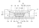
도1은 본 발명의 일 실시예에 따른 반도체 발광장치를 나타내는 평면도이다.
도2는 도1에 도시된 반도체 발광장치를 X1-X1'으로 절개하여 본 측단면도이다.
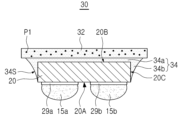
도3은 도1에 도시된 반도체 발광장치에 채용 가능한 발광소자를 나타내는 평면도이다.
도4는 도3에 도시된 발광소자를 X2-X2'로 절개하여 본 측단면도이다.
도5는 도3에 도시된 발광 소자에 채용 가능한 LED 칩을 나타내는 측단면도이다.
도6a 내지 도6e는 도1에 도시된 반도체 발광장치의 제조방법을 나타내는 주요 공정별 단면도이다.
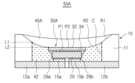
도7은 본 발명의 일 실시예에 따른 반도체 발광장치를 나타내는 측단면도이다.
도8은 도7에 도시된 반도체 발광장치에 채용 가능한 발광소자를 나타내는 측단면도이다.
도9a 내지 도9c는 도8에 도시된 반도체 발광소자의 제조방법을 나타내는 주요 공정별 단면도이다.
도10은 본 발명의 일 실시예에 따른 반도체 발광장치를 나타내는 측단면도이다.
도11은 본 발명의 일 실시예에 따른 디스플레이 장치를 나타내는 분해 사시도이다.
도12는 본 발명의 일 실시예에 따른 조명 장치를 나타내는 분해 사시도이다.1 is a plan view showing a semiconductor light emitting device according to an embodiment of the present invention.
Figure 2 is a side cross-sectional view of the semiconductor light emitting device shown in Figure 1 taken along line X1-X1'.
Figure 3 is a plan view showing a light-emitting element that can be employed in the semiconductor light-emitting device shown in Figure 1.
Figure 4 is a side cross-sectional view of the light emitting device shown in Figure 3 taken along line X2-X2'.
Figure 5 is a side cross-sectional view showing an LED chip that can be employed in the light-emitting device shown in Figure 3.
Figures 6A to 6E are cross-sectional views of each main process showing the manufacturing method of the semiconductor light emitting device shown in Figure 1.
Figure 7 is a side cross-sectional view showing a semiconductor light emitting device according to an embodiment of the present invention.
Figure 8 is a side cross-sectional view showing a light-emitting element applicable to the semiconductor light-emitting device shown in Figure 7.
Figures 9A to 9C are cross-sectional views of each main process showing the manufacturing method of the semiconductor light emitting device shown in Figure 8.
Figure 10 is a side cross-sectional view showing a semiconductor light emitting device according to an embodiment of the present invention.
Figure 11 is an exploded perspective view showing a display device according to an embodiment of the present invention.
Figure 12 is an exploded perspective view showing a lighting device according to an embodiment of the present invention.
이하, 첨부된 도면을 참조하여 본 발명의 다양한 실시예를 상세히 설명한다.
Hereinafter, various embodiments of the present invention will be described in detail with reference to the attached drawings.
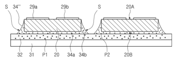
도1은 본 발명의 일 실시예에 따른 반도체 발광장치를 나타내는 평면도이며, 도2는 도1에 도시된 반도체 발광장치를 X1-X1'으로 절개하여 본 측단면도이다.Figure 1 is a plan view showing a semiconductor light emitting device according to an embodiment of the present invention, and Figure 2 is a side cross-sectional view taken along line X1-X1' of the semiconductor light emitting device shown in Figure 1.
도1 및 도2를 참조하면, 본 실시예에 따른 반도체 발광장치(50)는, 오목부(C)를 갖는 패키지 본체(10)와, 상기 오목부(C) 내에 탑재된 반도체 발광소자(30)와, 상기 오목부(C) 내에서 상기 반도체 발광소자(30)를 둘러싸는 반사성 수지부(42)를 포함한다. 1 and 2, the semiconductor
상기 패키지 본체(10)는 상기 오목부(C)를 정의하는 측벽(11)을 가지며, 상기 오목부(C)의 바닥면에 노출된 제1 및 제2 배선 전극(12a,12b)을 포함한다. 도1을 참조하면, 상기 오목부(C)의 평면 형상은 원형으로 예시되어 있으나, 이에 한정되지 않는다. 예를 들어, 상기 오목부(C)의 평면 형상은 칩 형상에 대응되는 형상을 가질 수 있다. The
상기 제1 및 제2 배선 전극(12a,12b)은 상기 패키지 본체(10)의 외부 표면(예, 하면 또는 측면)으로 연장될 수 있다. 상기 패키지 본체(10)는 절연성 수지일 수 있다. 일부 예에서, 상기 패키지 본체(10)는 반사성 분말이 분산된 몰딩 수지체를 포함할 수 있다. 예를 들어, 상기 백색 분말은 TiO2, Al2O3, Nb2O5 또는 ZnO과 같은 세라믹 분말을 포함할 수 있다. 상기 제1 및 제2 배선 전극(12a,12b)은 상기 패키지 본체(10)의 연결부(16)에 의해 결속된 한 쌍의 리드 프레임일 수 있다. 상기 제1 및 제2 배선 전극(12a,12b)는 Au, Cu, Ag, Al와 같은 금속을 포함할 수 있다. The first and
상기 패키지 본체(10)의 측벽(11)은 상기 오목부(C)에서 상기 제1 및 제2 배선 전극(12a,12b)의 표면과 이루는 각이 비교적 큰 각도(θ1)를 이룬다. 이러한 측벽(11)의 각도(θ1)를 증가시킴으로써 상기 패키지 본체(11)와 상기 제1 및 제2 배선 전극(12a,12bb)이 접하는 영역에서 몰딩체의 크랙 발생을 감소시킬 수 있다. 예를 들어, 측벽(11)의 각도(θ1)는 80°이상일 수 있으며, 특정 예에서 거의 수직일 수 있다. The
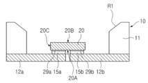
상기 반도체 발광소자(30)는, 서로 반대에 위치한 제1 및 제2 면(20A,20B)과 상기 제1 및 제2 면 사이에 위치한 측면들(20C)을 갖는 반도체 발광다이오드(LED) 칩(20)을 포함한다. The semiconductor
도2에 도시된 바와 같이, 상기 반도체 발광소자(30)는 상기 LED 칩(20)의 제1 면(20A)이 상기 오목부(C)의 바닥면을 향하도록 상기 오목부(C) 내에 탑재될 수 있다. 상기 LED 칩(20)은 상기 제1 면에 배치된 제1 및 제2 전극(29a,29b)을 포함한다. 상기 제1 및 제2 전극(29a,29b)은 솔더와 같은 도전성 범프(15a,15b)를 이용하여 상기 제1 및 제2 배선 전극(12a,12b) 각각에 연결될 수 있다.
As shown in Figure 2, the semiconductor
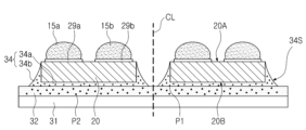
도3 및 도4를 참조하면, 본 실시예에 채용된 반도체 발광소자(30)가 개별 디바이스로 도시되어 있다. 본 실시예에서, 상기 반도체 발광소자(30)는 도4에 도시된 형태로 먼저 제조된 후에 패키지 본체(10)에 탑재될 수 있으나, 이와 달리 LED 칩(20)을 패키지 본체(10)에 탑재한 후에 상기 반도체 발광소자의 다른 구성(파장변환 필름 등)을 부가하는 방식이 사용될 수도 있다(도6a 내지 도6e 참조).
3 and 4, the semiconductor
도4에 도시된 바와 같이, 상기 반도체 발광소자(30)는 상기 LED 칩(20)의 제2 면(20B)에 배치된 파장변환 필름(32)과, 상기 LED 칩(20)과 상기 파장변환 필름(32)을 접합하는 광투과성 접합층(34)을 포함할 수 있다.As shown in Figure 4, the semiconductor
상기 파장변환 필름(32)은 상기 LED 칩(20)으로부터 방출된 광의 일부를 방출 파장과 다른 제1 파장의 광으로 변환하는 제1 파장변환물질(P1)을 포함한다. 상기 파장변환 필름(32)은 상기 제1 파장변환 물질(P1)이 분산된 수지층 또는 세라믹 형광체 필름일 수 있다. 예를 들어, 상기 파장변환 필름(32)은 형광체 또는 양자점과 같은 제1 파장변환 물질(P1)이 함유된 글래스층일 수 있다. The
상기 파장변환 필름(32)은 상기 반도체 발광다이오드 칩(20)의 면적보다 큰 면적을 가질 수 있다. 상기 파장변환 필름(32)은 상기 LED 칩(20)의 제2 면(20B)을 덮도록 배치될 수 있다. 도3에 도시된 바와 같이, 상기 파장변환 필름(32)은 LED 칩(20)에 의해 커버되지 않으면서 LED 칩(20)을 둘러싸는 외주 영역을 가지며, 그 외주 영역을 따라 광투과성 접합층(34)이 연장될 수 있다.The
본 실시예에 채용된 광투과성 접합층(34)은 도4에 도시된 바와 같이, 상기 파장변환 필름(32)과 상기 LED 칩(20) 사이에 위치한 접착 영역(34a)과, 상기 LED 칩(20)의 측면(20C)을 따라 위치한 측부 연장 영역(34b)을 가질 수 있다. 상기 측부 연장 영역(34b)은 상기 LED 칩(20)의 측면들(20C)로 연장되며 상기 오목부(C)의 바닥면을 향하여 경사진 표면(34S)을 갖는다. As shown in Figure 4, the light-
상기 측부 연장 영역(34b)은 상기 광투과성 필름(32)에 가까울수록 증가하는 폭을 가질 수 있다. 이러한 측부 연장 영역(34b)의 단면 형상은 광투과성 접합층(34)을 위한 수지의 점도 및/또는 양에 따라 달라질 수 있다(도6b 및 도6c 참조). 예를 들어, 상기 광투과성 접합층(34)은 실리콘(silicone), 에폭시, 폴리아크릴레이트, 폴리이미드, 폴리 아마이드 또는 벤조사이클로부텐을 포함할 수 있다.The
도2에 도시된 바와 같이, 상기 반도체 발광소자(30)는 오목부(C) 내에 탑재되어 상기 반사성 수지부(42)에 의해 둘러싸일 수 있다. 상기 반사성 수지부(42)는 반사성 분말이 함유된 광투과성 수지로 이루어질 수 있다. 본 실시예에 채용된 측면 연장 영역(34)은 파장변환물질이 함유된 광투과성 수지로 이루어질 수 있다. 예를 들어, 상기 광투과성 수지는 실리콘(silicone) 수지일 수 있다. 실리콘 수지의 굴절률은 1.38∼1.8 범위에서 선택될 수 있다. 상기 반사성 분말은 백색 세라믹 분말 또는 금속 분말일 수 있다. 예를 들어, 상기 세라믹 분말은 TiO2, Al2O3, Nb2O5 및 ZnO로 구성된 그룹으로부터 선택된 적어도 하나일 수 있다. 상기 금속 분말은 Al 또는 Ag와 같은 물질일 수 있다.As shown in Figure 2, the semiconductor
본 실시예에서, 상기 반사성 수지부(42)는 상기 광투과성 접합층(34)과의 계면을 가질 수 있다. 이러한 계면은 측부 연장 영역(34b)의 경사면(34S)을 따라 제공되며, 상기 LED 칩(20)의 측방향으로 진행하는 빛에 대해 반사면으로 작용할 수 있다. 즉, 상기 계면은 상기 LED 칩(20)의 측방향으로 진행하는 빛은 상기 파장변환 필름(32)으로 향하도록 반사될 수 있고, 반도체 발광장치(50)의 광추출효율을 개선할 수 있다.In this embodiment, the
한편, 상기 반사성 수지부(42)는 상기 LED 칩의 제1 면과 상기 오목부의 바닥면 사이에서 상기 반도체 상기 도전성 범프(15a,15b)를 둘러싸도록 형성될 수 있다. 이와 같이, 상기 반사성 수지부(42)를 이용하여 도전성 범프들(15a,15b)에 광이 흡수되는 것을 효과적으로 방지할 수 있다. 또한, 상기 반사성 수지부(42)는 상기 LED 칩(20)의 제1 면(20A)과 상기 오목부(C)의 바닥면 사이의 공간을 거의 충전함으로써 아래 방향으로 진행하는 광을 원하는 추출 방향(예, 파장변환 필름(32)의 방향)으로 가이드할 수 있다. Meanwhile, the
본 실시예에서, 도2에 도시된 바와 같이, 상기 패키지 본체(10)의 측벽(11)은 경사진 제1 반사면(R1)을 가질 수 있다. 상기 반사성 수지부(42)의 상면은 상기 제1 반사면(R1)에 연결된 제2 반사면(R2)으로 제공될 수 있다. 상기 제1 및 제2 반사면(R1,R2)은 광추출에 유리하도록 대체로 낮은 경사각을 가질 수 있다. 예를 들어, 상기 제1 및 제2 반사면(R1,R2)의 경사각은 20∼40°범위일 수 있다. 상기 제1 및 제2 반사면(R1,R2)의 경사각은 서로 다르게 설정될 수 있다. In this embodiment, as shown in Figure 2, the
상기 반사성 수지부(42)는 액상 수지의 경화공정에 의해 형성되므로, 상기 제2 반사면(R2)은 메니스커스(meniscus)와 유사한 곡면을 가질 수 있다. 이러한 경사진 반사면(R2)을 제공하기 위해서, 상기 반사성 수지부(42)의 상면은 상기 측벽(11)에 접하는 제1 레벨(L1)이 상기 LED 칩(20)에 인접한 제2 레벨(L2)보다 높게 형성될 수 있다. 상기 제2 레벨(L2)은 파장변환 필름(32) 상단에 의해 결정될 수 있다.
Since the
도2를 참조하면, 파장변환 수지층(45)은 상기 파장변환 필름(32) 상에 배치될 수 있다. 상기 파장변환 수지층(45)은 상기 반사성 수지부(42) 상면의 적어도 일부에 연장될 수 있다. 상기 파장변환 수지층(45)은 제2 파장변환 물질(P2)을 함유하는 광투과성 수지로 형성될 수 있다. 상기 제2 파장변환 물질(P2)은 상기 LED 칩(20)으로부터 방출된 광의 일부를 방출 파장과 다른 제2 파장의 광으로 변환하는 형광체 또는 양자점일 수 있다. 상기 제2 파장변환 물질(P2)은 상기 제1 파장변환 물질(P1)의 변환 광의 파장보다 짧은 파장의 변환된 광을 제공할 수 있다. Referring to Figure 2, the wavelength
예를 들어, 상기 반도체 발광장치(50)는 백색 광을 방출할 수 있다. 일부 실시예에서, 상기 LED 칩(20)은 청색광을 방출할 수 있다. 예를 들어, 상기 LED 칩(20)은 440㎚∼460㎚ 범위인 주파장을 갖는 광을 방출할 수 있다. 상기 제1 파장변환 물질(P1)은 청색광의 일부를 적색으로 변환하는 형광체 또는 양자점일 수 있다. 상기 제2 파장변환 물질(P2)은 청색광의 일부를 황색 및/또는 녹색으로 변환하는 형광체 또는 양자점일 수 있다. For example, the semiconductor
본 실시예에 채용된 파장변환 필름(32)은 소정의 광투과율을 갖도록 구성하여 파장변환 수지층(45)에 LED 칩의 방출광을 제공할 수 있다. 상기 파장변환 필름(32)의 원하는 광투과율은 제1 파장변환 물질(P1)의 함유율을 적절히 조절함으로써 얻어질 수 있다. 예를 들어, 상기 파장변환 필름(32) 중 제1 파장변환물질(P1)은 5∼30 vol% 범위로 함유될 수 있다.
The
본 실시예에 채용 가능한 LED 칩(20)의 일 예가 도5에 도시되어 있다. An example of an
도5를 참조하면, 상기 LED 칩(20)은, 기판(21)과, 상기 기판(21) 상에 순차적으로 배치된 제1 도전형 반도체층(24), 활성층(25) 및 제2 도전형 반도체층(26)을 포함한다. Referring to Figure 5, the
상기 기판(21)은 사파이어와 같은 절연성 기판일 수 있으나, 이에 한정되지 않는다. 상기 기판(21)은 절연성 외에도 도전성 또는 반도체 기판일 수 있다. 예를 들어, 상기 기판(21)은 사파이어 외에도 SiC, Si, MgAl2O4, MgO, LiAlO2, LiGaO2, GaN일 수 있다. 상기 기판(21)의 상면에는 요철(P)이 형성될 수 있다. 상기 요철(P)은 광추출효율을 개선하면서 성장되는 단결정의 품질을 향상시킬 수 있다.The
상기 기판(21)과 상기 제1 도전형 반도체층(24) 사이에 버퍼층(22)이 배치될수 있다. 상기 버퍼층(22)은 InxAlyGa1 -x- yN (0≤x≤1, 0≤y≤1)일수 있다. 예를 들어, 상기 버퍼층(22)는 GaN, AlN, AlGaN, InGaN일 수 있다. 일부 예에서는, 복수의 층을 조합하거나, 조성을 점진적으로 변화시켜 사용할 수도 있다.A buffer layer 22 may be disposed between the
상기 제1 도전형 반도체층(24)은 n형 InxAlyGa1 -x- yN (0≤x<1, 0≤y<1, 0≤x+y<1)을 만족하는 질화물 반도체일 수 있으며, n형 불순물은 Si일 수 있다. 예를 들어, 상기 제1 도전형 반도체층(24)은 n형 GaN을 포함할 수 있다. 상기 제2 도전형 반도체층(26)은 p형 InxAlyGa1 -x- yN (0≤x<1, 0≤y<1, 0≤x+y<1)을 만족하는 질화물 반도체층일 수 있으며, p형 불순물은 Mg일 수 있다. 다른 예에서, 상기 제2 도전형 반도체층(26)은 서로 다른 조성을 갖는 다층 구조를 가질 수 있다. The first
상기 활성층(25)은 양자우물층과 양자장벽층이 서로 교대로 적층된 다중 양자우물(MQW) 구조일 수 있다. 예를 들어, 상기 양자우물층과 양자장벽층은 서로 다른 조성을 갖는 InxAlyGa1 -x- yN (0≤x≤1, 0≤y≤1, 0≤x+y≤1)일 수 있다. 특정 예에서, 상기 양자우물층은 InxGa1 - xN (0<x≤1)이며, 상기 양자장벽층은 GaN 또는 AlGaN일 수 있다. 양자우물층과 양자장벽층의 두께는 각각 1㎚∼50㎚ 범위일 수 있다. 상기 활성층(25)은 다중 양자우물 구조에 한정되지 않고, 단일 양자우물 구조일 수 있다. The
상기 제1 및 제2 전극(29a,29b)은, 동일한 제1 면(20A)에 위치하도록, 상기 제1 도전형 반도체층(24)의 메사 에칭된 영역과 상기 제2 도전형 반도체층(26)에 각각 배치될 수 있다. 상기 제1 전극(29a)은 이에 한정되지 않지만, Ag, Ni, Al, Cr, Rh, Pd, Ir, Ru, Mg, Zn, Pt, Au 등의 물질을 포함할 수 있으며, 단일층 또는 2층 이상의 구조로 채용될 수 있다. 상기 제2 전극(29b)은 Al, Au, Cr, Ni, Ti, Sn 중 적어도 하나를 포함할 수 있다. 일부 실시예에서, 상기 제2 전극(29b)은 투명 전도성 산화물 또는 투명 전도성 질화물과 같은 투명 전극이거나, 그래핀(graphene)을 포함할 수 있다..
The first and
도6a 내지 도6e는 도1에 도시된 반도체 발광장치의 제조방법을 나타내는 주요 공정별 단면도이다. Figures 6A to 6E are cross-sectional views of each main process showing the manufacturing method of the semiconductor light emitting device shown in Figure 1.
도6a을 참조하면, LED 칩(20)을 패키지 본체(10)의 오목부(C)에 탑재한다. Referring to Figure 6a, the
상기 LED 칩(20)은 상기 제1 면(20A)이 상기 오목부의 바닥면과 마주하도록 탑재될 수 있다. 상기 LED 칩(20)의 제1 면(20A)에 위치한 제1 및 제2 전극(29a,29b)은 솔더볼과 같은 도전성 범프(15a,15b)을 이용하여 각각 상기 제1 및 제2 배선 전극(12a,12b)에 연결될 수 있다.
The
도6b을 참조하면, LED 칩(20)의 제2 면(20B)에 미경화된 접합용 수지(34')를 적하한다. Referring to FIG. 6B, uncured bonding resin 34' is dropped onto the
이러한 적하공정은 디스펜싱 장치(D)를 이용하여 구현될 수 있다. 상기 접합용 수지(34')는 실리콘, 에폭시 또는 그 조합으로 이루어진 수지일 수 있다. 본 공정에서는, 접합에 필요한 양보다 많은 양으로 적하할 수 있다. 즉, 후속되는 접합공정에서 LED 칩(20)의 측면을 따라 접합용 수지(34')의 일부가 흘러 내려 경사부를 형성할 정도의 충분한 양으로 제공될 수 있다. 상기 접합용 수지는 분말형태의 광분산재를 포함할 수 있다. 예를 들어, 광분산재는 SiO2, TiO2 또는 Al2O3을 포함할 수 있다.
This dropping process can be implemented using a dispensing device (D). The bonding resin 34' may be a resin made of silicone, epoxy, or a combination thereof. In this process, a larger amount than that required for bonding can be added dropwise. That is, in the subsequent bonding process, a portion of the bonding resin 34' may flow down along the side of the
도6c을 참조하면, 파장변환 필름(32)을 접합용 수지(34')가 적용된 LED 칩(20)의 제2 면(20B)에 배치한다. Referring to Figure 6c, the
상기 파장변환 필름(32)은 제1 파장변환 물질(P1)을 함유한 필름일 수 있다. 상기 파장변환 필름(32)의 배치과정에서, 접합용 수지(34')의 일부는 LED 칩(20)의 측면(20C)을 따라 흘러내리고, 경화 전까지 흘러내린 부분이 표면 장력에 의해 상기 칩(20)의 측면에서 경사면(S)을 이루면서 유지될 수 있다. 이러한 경사면(S)의 형상은 접합용 수지(34')의 점도이나 파장변환 필름(32)의 외주 영역(LED 칩의 바깥 부분)의 면적에 따라 조절될 수 있다. 예를 들어, 큰 면적의 파장변환 필름(32)을 사용하여 외주 영역을 확장하고, 접합용 수지(34')의 점도를 적정한 수준으로 높임으로써 바닥면에 대한 경사각(θ2)을 낮출 수 있으며, 경사면을 이루는 수지 부분을 확장시킬 수 있다.
The
도6d를 참조하면, 파장변환 필름(32)이 LED 칩(20)의 제2 면(20B)에 접합되도록 접합용 수지(34')를 경화시킨다. Referring to Figure 6d, the bonding resin 34' is cured so that the
본 경화 공정에서, 접합용 수지(34')가 경화되어 광투과성 접합층(34)을 형성할 수 있다. 상기 광투과성 접합층(34)은 상기 파장변환 필름(32)과 상기 LED 칩(20) 사이에 위치한 접착 영역(34a)을 포함한다. 또한, 상기 LED 칩(20)의 측면을 따라 경사지게 흘러내린 접합용 수지(42') 부분은 측부 연장 영역(34b)로 제공될 수 있다. 상기 측부 연장 영역(34b)은 상기 LED 칩(20)의 측면(20C)에 위치하며 상기 오목부(C)의 바닥면을 향하여 경사진 면(34S)을 제공하도록 구성될 수 있다. 본 공정에 의해, 상기 측부 연장 영역(34b)은 광추출에 유리한 경사진 면을 제공함으로써 상기 LED 칩(20)의 측면에서의 내부 전반사를 감소시켜 광추출효율을 개선할 수 있다.
In this curing process, the bonding resin 34' is cured to form a light-
도6e을 참조하면, LED 칩(20)을 둘러싸도록 오목부(C) 내에 반사성 수지부(42)를 형성할 수 있다. Referring to Figure 6e, the
상기 반사성 수지부(42)는 상기 광투과성 접합층(34)의 측부 연장 영역(34b)와의 계면을 형성하고, 이러한 경사진 계면은 상기 파장변환 필름(32)을 향해 빛을 안내시키는 반사면으로 제공될 수 있다. 상기 반사성 수지부(42)는 반사성 분말이 함유된 광투과성 수지로 이루어질 수 있다. 예를 들어, 상기 반사성 분말은 TiO2, Al2O3, Nb2O5, Al2O3 또는 ZnO인 백색 세라믹 분말일 수 있다.
The
도6e에 도시된 결과물의 파장변환 필름(32) 상에 파장변환 수지층(42)을 추가적으로 형성함으로써, 도2에 도시된 반도체 발광장치(50)가 제조될 수 있다. 상기 파장변환 수지층(42)은 제2 파장변환 물질(P2)을 함유한 광투과성 액상 수지를 이용하여 형성될 수 있다. 상기 파장변환 수지층(42) 형성은 디스펜싱 공정을 이용하여 수행될 수 있다.
The semiconductor
도7은 본 발명의 일 실시예에 따른 반도체 발광장치를 나타내는 측단면도이며, 도8은 도7에 도시된 반도체 발광장치에 채용 가능한 발광소자를 나타내는 측단면도이다. Figure 7 is a side cross-sectional view showing a semiconductor light-emitting device according to an embodiment of the present invention, and Figure 8 is a side cross-sectional view showing a light-emitting element applicable to the semiconductor light-emitting device shown in Figure 7.
도7에 도시된 반도체 발광장치(50A)은 파장변환물질의 배치만을 제외하고 도1에 도시된 반도체 발광장치(50)과 유사한 것으로 이해할 수 있다. 본 실시예의 구성요소는 특별히 반대되는 설명이 없는 한 도2에 도시된 반도체 발광장치(50)의 동일하거나 유사한 구성요소에 대한 설명을 참조하여 이해될 수 있다.The semiconductor
본 실시예에서는, 광투과성 접합층(34)은 제1 파장변환 물질(P1)을 함유한 광투성 접합 수지로 이루어지며, 파장변환 필름(32)은 제2 파장변환 물질(P2)을 포함한다. 상기 LED 칩(20)은 청색 LED 칩 또는 UV LED 칩일 수 있다. 상기 제1 파장변환 물질(P1)은 상기 LED 칩(20)으로부터 방출된 광의 일부를 그와 다른 제1 파장을 변환하는 형광체 또는 양자점일 수 있다. 상기 제2 파장변환 물질(P2)은 상기 LED 칩(20)의 방출광을 상기 제1 광의 파장보다 짧은 파장의 제2 광으로 변환하는 형광체 또는 양자점일 수 있다. 상기 광투과성 접합 수지는, 실리콘, 에폭시, 폴리아크릴레이트, 폴리이미드, 폴리 아마이드 또는 벤조사이클로부텐을 포함할 수 있다. In this embodiment, the light-
본 실시예에 채용된 수지층(45A)에는 파장변환 물질이 함유되지 않을 수 있다. 물론, 필요에 따라 추가적인 파장변환 물질을 수지층에 함유시킬 수 있다. The
도8에 도시된 반도체 발광소자(30A)에서, 광투과성 접합층(34)은 상기 광투과성 필름(32)과 상기 LED 칩(20) 사이에 위치한 접착 영역(34a)과, 상기 LED 칩(20)의 측면(20C)을 따라 위치한 측부 연장 영역(34b)를 가질 수 있다. 광투과성 접합층(34)의 접착영역(34a)은 접합강도를 유지하기 위한 적정한 두께(t)를 가질 수 있다. 예를 들어, 접합층의 구성물질에 따라 다를 수 있으나, 접착 영역(34a)의 두께(t)는 적어도 15㎛일 수 있다. 접착영역(34a)의 두께(t)는 원하는 접합 강도 외에 채용되는 형광체와 같은 파장변환물질의 크기와 양에 따라 변경될 수 있다. 일부 실시예에서, 상기 접착 영역(34a)의 두께(t)는 채용되는 형광체의 입도(d50)(예, 5∼40㎛)보다는 큰 두께로 설계될 수 있으며, 많은 양의 형광체가 요구될 경우에 그 입도보다 훨씬 크게 증가될 수 있다. 일부 예에서, 상기 접합 영역(34a)의 두께(t)는 50㎛이상일 수 있다.
In the semiconductor
본 실시예에 채용된 복수의 파장변환물질들(P1,P2)은, 변환 파장에 따라 광투과성 필름(32)과 광투과성 접합층(34)으로 구분되어 배치될 수 있다. 상기 LED 칩(20)과 인접한 광투과성 접합층(34)에는 상대적으로 장파장의 광을 제공하기 위한 제2 파장변환 물질(P2)이 도입되는 반면에, 상기 광투과성 필름(32)에는 상대적으로 단파장의 광을 제공하기 위한 제1 파장변환 물질(P1)이 도입된다.
The plurality of wavelength conversion materials (P1, P2) employed in this embodiment may be arranged separately into a light-transmitting
앞선 실시예에 따른 공정(도6a 내지 도6e)은 베어 LED 칩을 이용하는 공정으로 설명하였으나, 이와 달리 도4에 도시된 반도체 발광소자를 미리 제조한 후에 패키지 제조공정을 수행하는 방식으로 구현될 수 있다. The process according to the previous embodiment (FIGS. 6A to 6E) was described as a process using a bare LED chip. However, unlike this, it can be implemented by performing a package manufacturing process after pre-manufacturing the semiconductor light emitting device shown in FIG. 4. there is.
도9a 내지 도9c는 도8에 도시된 반도체 발광소자의 제조방법을 나타내는 주요 공정별 단면도이다.
Figures 9A to 9C are cross-sectional views of each main process showing the manufacturing method of the semiconductor light emitting device shown in Figure 8.
도9a를 참조하면, 파장변환 필름(32)을 베이스 필름(31) 상에 배치하고, 파장변환 필름 상에 미경화 상태의 접합용 수지(34)를 적하시킨다. Referring to Figure 9a, the
상기 파장변환 필름(32)은 제1 파장변환 물질(P1)을 포함할 수 있다. 상기 파장변환 필름(32)은 다양한 형태로 제공될 수 있다. 예를 들어, 상기 파장변환 필름(32)은 수지층 또는 세라믹 필름일 수 있다. 일부 예에서, 상기 파장변환 필름(32)은 형광체 또는 양자점과 같은 제1 파장변환 물질(P1)이 함유된 글래스층일 수 있다. 이러한 글래스층은 저온(예, 400℃이하) 소성 글래스일 수 있다. 이러한 적하 위치 및 영역은 원하는 반도체 발광장치의 면적을 고려하여 규칙적으로 배열될 수 있다.
The
도9b에 도시된 바와 같이, 상기 접합 수지(34") 상에 상기 복수의 LED 칩(20)을 배치할 수 있다. As shown in Figure 9b, the plurality of
이러한 배치과정에서, 상기 접합에 사용된 양을 제외하고, 미경화된 접합 수지(34")는 LED 칩(20)의 측면에 따라 상승할 수 있다. 이러한 측면에 따른 상승 정도와 표면 형상은 접합 수지(34")의 점도 및 양을 이용하여 조절할 수 있다. 접합 수지(34')의 점도는 분말 타입의 칙소재를 첨가시킴으로써 제어될 수 있다. 예를 들어, 칙소재로는 실리카(silica) 입자가 사용될 수 있다.
In this arrangement process, except for the amount used for the bonding, the
도9c를 참조하면, 파장변환 필름(32)과 LED 칩(20)이 접합되도록 접합용 수지(34")를 경화시켜 광투과성 접합층(34)을 형성할 수 있다. Referring to Figure 9c, the light-
상기 광투과성 접합층(34)은 상기 파장변환 필름(32)과 상기 LED 칩(20) 사이에 위치한 접착 영역(34a)을 포함하고, 상기 LED 칩(20)의 측면을 따라 경사지게 흘러내린 부분은 측부 연장 영역(34b)으로 제공될 수 있다. 앞서 설명한 바와 같이, 이러한 측부 연장 영역(34b)은 광추출에 유리한 경사진 면(34S)을 제공함으로써 상기 LED 칩(20)의 측면에서의 내부 전반사를 감소시켜 광추출효율을 개선할 수 있다. 일부 실시에에서, 상기 경사진 표면(34S)은 미경화 상태의 접합 수지에 의해 형성된 오목한 면, 즉 메니스커스 형상을 가질 수 있다. 이어, 절단선(CL)을 따라 소자 단위로 절단함으로써 도8에 도시된 반도체 발광소자(30A)를 얻을 수 있다.
The light-transmitting
도10은 본 발명의 일 실시예에 따른 반도체 발광장치를 나타내는 측단면도이다. Figure 10 is a side cross-sectional view showing a semiconductor light emitting device according to an embodiment of the present invention.
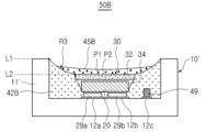
도10에 도시된 반도체 발광장치(50B)은 패키지 본체(10') 구조와 제너 다이오드(49)가 포함된 점을 제외하고 도1에 도시된 반도체 발광장치(50)과 유사한 것으로 이해할 수 있다. 본 실시예의 구성요소는 특별히 반대되는 설명이 없는 한, 도1에 도시된 반도체 발광장치(50)의 동일하거나 유사한 구성요소에 대한 설명을 참조하여 이해될 수 있다.The semiconductor
상기 패키지 본체(10')는 앞선 실시예와 유사하게 상기 오목부(C)를 정의하는 측벽(11')을 갖는다. 상기 측벽(11')은 상기 오목부(C)의 바닥면에서 거의 수직으로 형성될 수 있다. 본 실시예에서는, 패키지 본체(10')는 별도의 경사진 반사면을 갖지 않도록 구성하는 대신에, 반사성 수지층(42B)의 상면을 이용하여 반사면을 제공할 수 있다. 상기 반사성 수지부(42B)의 상면을 상기 측벽(11')의 상단에 접하는 제1 레벨(L1)에서 상기 LED 칩(20)에 인접한 제2 레벨(L2)로 연장되도록 구성함으로써 경사진 반사면(R3)을 제공할 수 있다. 이러한 경사진 반사면(R3)은 20∼40°범위의 낮은 경사각을 가지며, 전체적으로 메니스커스 형상과 같은 곡면을 가질 수 있다. 상기 패키지 본체(10')는, 반사성 분말이 분산된 몰딩 수지체를 포함할 수 있다. 예를 들어, 상기 백색 분말은 TiO2, Al2O3, Nb2O5 또는 ZnO과 같은 세라믹 분말을 포함할 수 있다. The package body 10' has a side wall 11' defining the concave portion C, similar to the previous embodiment. The side wall 11' may be formed almost vertically on the bottom surface of the concave portion C. In this embodiment, the package body 10' may be configured not to have a separate inclined reflective surface, but may instead provide a reflective surface using the upper surface of the reflective resin layer 42B. An inclined reflective surface is formed by configuring the upper surface of the reflective resin portion 42B to extend from the first level L1 adjacent to the top of the side wall 11' to the second level L2 adjacent to the
상기 패키지 본체(10')는 상기 제1 및 제2 배선 전극(12a,12b)과 함께 제너다이오드(49)를 연결하기 위한 제3 배선 전극(12c)을 더 포함할 수 있다. 상기 제3 배선 전극(12c)은 오목부(C)의 일측에 마련될 수 있다. 상기 오목부(C)의 바닥면은 평탄한 면으로 이루어지며, 제너 다이오드(49)는 상기 평탄한 면 상에 LED 칩(20)과 함께 배치되어 제3 배선 전극(12c)에 전기적으로 연결될 수 있다. The package body 10' may further include a
본 실시예에 채용된 제너 다이오드(49)는 광을 흡수하는 요소로 작용할 수 있지만, 오목부(C) 내에서 반사성 수지부(42B)에 의해 둘러싸이므로, 제너 다이오드(49)에 의한 광효율 저하를 방지할 수 있다. 도10에 도시된 바와 같이, 파장변환 수지층(45B)은 앞선 실시예에 비해 얇게 제공될 수 있으며, 제2 파장변환 물질(P2)이 조밀하게 배치될 수 있다.
The
도11은 본 발명의 일 실시예에 따른 디스플레이 장치를 나타내는 분해사시도이다.Figure 11 is an exploded perspective view showing a display device according to an embodiment of the present invention.
도11을 참조하면, 디스플레이 장치(3000)는, 백라이트 유닛(3100), 광학시트(3200) 및 액정 패널과 같은 화상 표시 패널(3300)을 포함할 수 있다. Referring to FIG. 11, the
백라이트 유닛(3100)은 바텀케이스(3110), 반사판(3120), 도광판(3140) 및 도광판(3140)의 적어도 일 측면에 제공되는 광원모듈(3130)을 포함할 수 있다. 광원모듈(3130)은 인쇄회로기판(3131) 및 광원(3132)을 포함할 수 있다. 여기에 사용되는 광원(3132)은 앞서 설명된 실시예에 따른 반도체 발광장치일 수 있다. The
광학시트(3200)는 도광판(3140)과 화상 표시 패널(3300)의 사이에 배치될 수 있으며, 확산시트, 프리즘시트 또는 보호시트와 같은 여러 종류의 시트를 포함할 수 있다. The
화상 표시 패널(3300)은 광학시트(3200)를 출사한 광을 이용하여 영상을 표시할 수 있다. 화상 표시 패널(3300)은 어레이 기판(3320), 액정층(3330) 및 컬러 필터 기판(3340)을 포함할 수 있다. 어레이 기판(3320)은 매트릭스 형태로 배치된 화소 전극들, 상기 화소 전극에 구동 전압을 인가하는 박막 트랜지스터들 및 상기 박막 트랜지스터들을 작동시키기 위한 신호 라인들을 포함할 수 있다. 컬러 필터 기판(3340)은 투명기판, 컬러 필터 및 공통 전극을 포함할 수 있다. 상기 컬러 필터는 백라이트 유닛(3100)으로부터 방출되는 백색광 중 특정 파장의 광을 선택적으로 통과시키기 위한 필터들을 포함할 수 있다. 액정층(3330)은 상기 화소 전극 및 상기 공통 전극 사이에 형성된 전기장에 의해 재배열되어 광투과율을 조절할 수 있다. 광투과율이 조절된 광은 컬러 필터 기판(3340)의 상기 컬러 필터를 통과함으로써 영상을 표시할 수 있다. 화상 표시 패널(3300)은 영상 신호를 처리하는 구동회로 유닛 등을 더 포함할 수 있다.
The
도12는 본 발명의 일 실시예에 따른 벌브형 조명장치를 나타내는 분해사시도이다.Figure 12 is an exploded perspective view showing a bulb-type lighting device according to an embodiment of the present invention.
도12에 도시된 조명 장치(4200)는 소켓(4210), 전원부(4220), 방열부(4230), 광원모듈(4240) 및 광학부(4250)를 포함할 수 있다. 본 발명의 예시적 실시예에 따라, 광원모듈(4240)은 발광다이오드 어레이를 포함할 수 있고, 전원부(4220)는 발광다이오드 구동부를 포함할 수 있다.The lighting device 4200 shown in FIG. 12 may include a
소켓(4210)은 기존의 조명 장치와 대체 가능하도록 구성될 수 있다. 조명 장치(4200)에 공급되는 전력은 소켓(4210)을 통해서 인가될 수 있다. 도시된 바와 같이, 전원부(4220)는 제1 전원부(4221) 및 제2 전원부(4222)로 분리되어 조립될 수 있다. 방열부(4230)는 내부 방열부(4231) 및 외부 방열부(4232)를 포함할 수 있고, 내부 방열부(4231)는 광원모듈(4240) 및/또는 전원부(4220)와 직접 연결될 수 있고, 이를 통해 외부 방열부(4232)로 열이 전달되게 할 수 있다. 광학부(4250)는 내부 광학부(미도시) 및 외부 광학부(미도시)를 포함할 수 있고, 광원모듈(4240)이 방출하는 빛을 고르게 분산시키도록 구성될 수 있다.The
광원모듈(4240)은 전원부(4220)로부터 전력을 공급받아 광학부(4250)로 빛을 방출할 수 있다. 광원모듈(4240)은 하나 이상의 광원(4241), 회로기판(4242) 및 컨트롤러(4243)를 포함할 수 있고, 컨트롤러(4243)는 발광다이오드(4241)들의 구동 정보를 저장할 수 있다. 여기에 사용되는 광원(4241)은 앞서 설명된 실시예에 따른 반도체 발광장치일 수 있다. The
본 실시예에 따른 조명 장치(4300)에서 광원 모듈(4240)의 상부에 반사판(4310)이 포함되어 있으며, 반사판(4310)은 광원으로부터의 빛을 측면 및 후방으로 고르게 퍼지게 하여 눈부심을 줄일 수 있다.In the
반사판(4310)의 상부에는 통신 모듈(4320)이 장착될 수 있으며 상기 통신 모듈(4320)을 통하여 홈-네트워크(home-network) 통신을 구현할 수 있다. 예를 들어, 상기 통신 모듈(4320)은 지그비(Zigbee), 와이파이(WiFi) 또는 라이파이(LiFi)를 이용한 무선 통신 모듈일 수 있으며, 스마트폰 또는 무선 컨트롤러를 통하여 조명 장치의 온(on)/오프(off), 밝기 조절 등과 같은 가정 내외에 설치되어 있는 조명을 컨트롤 할 수 있다. 또한 상기 가정 내외에 설치되어 있는 조명 장치의 가시광 파장을 이용한 라이파이 통신 모듈을 이용하여 TV, 냉장고, 에어컨, 도어락, 자동차 등 가정 내외에 있는 전자 제품 및 자동차 시스템의 컨트롤을 할 수 있다. 상기 반사판(4310)과 통신 모듈(4320)은 커버부(4330)에 의해 커버될 수 있다.
A
본 발명은 상술한 실시형태 및 첨부된 도면에 의해 한정되는 것이 아니며, 첨부된 청구범위에 의해 한정하고자 한다. 따라서, 청구범위에 기재된 본 발명의 기술적 사상을 벗어나지 않는 범위 내에서 당 기술분야의 통상의 지식을 가진 자에 의해 다양한 형태의 치환, 변형 및 변경이 가능할 것이며, 이 또한 본 발명의 범위에 속한다고 할 것이다.
The present invention is not limited by the above-described embodiments and the attached drawings, but is intended to be limited by the attached claims. Accordingly, various forms of substitution, modification, and change may be made by those skilled in the art without departing from the technical spirit of the present invention as set forth in the claims, and this also falls within the scope of the present invention. something to do.
10, 10': 패키지 본체
12a,12b: 제1 및 제2 배선 전극
15a,15b: 도전성 범프
20: 반도체 발광다이오드(LED) 칩
29a,29b: 제1 및 제2 전극
32: 파장변환 필름
34: 광투과성 접합층
42: 반사성 수지부
45: 파장변환 수지층10, 10': package body
12a, 12b: first and second wiring electrodes
15a, 15b: conductive bumps
20: Semiconductor light-emitting diode (LED) chip
29a, 29b: first and second electrodes
32: Wavelength conversion film
34: Light-transmissive bonding layer
42: reflective resin portion
45: Wavelength conversion resin layer
Claims (20)
제1 및 제2 전극이 배치된 제1 면과 상기 제1 면과 반대에 위치한 제2 면과 상기 제1 및 제2 면 사이에 위치한 측면들을 가지며, 상기 제1 면이 상기 바닥면을 향하도록 상기 오목부에 탑재된 LED 칩;
상기 제1 및 제2 전극을 상기 제1 및 제2 배선 전극에 각각 연결된 도전성 범프들;
상기 LED 칩의 제2 면에 배치되며 제1 파장변환 물질을 함유하는 파장변환 필름;
상기 LED 칩의 제2 면과 상기 파장변환 필름 사이에 배치되어 상기 LED 칩과 상기 파장변환 필름을 접합하는 광투과성 접합층;
상기 LED 칩을 둘러싸도록 상기 오목부 내에 배치되며, 상기 LED 칩의 제1 면과 상기 오목부의 바닥면 사이의 공간에 충전된 반사성 수지부; 및
상기 파장변환 필름과 상기 반사성 수지부 상에 배치되며, 제2 파장변환 물질을 함유하는 광투과성 수지를 갖는 파장변환 수지층;을 포함하고,
상기 반사성 수지부의 상면은 상기 오목부의 측벽에 접하는 레벨이 상기 LED 칩에 인접한 레벨보다 높게 형성되는 반도체 발광장치.
a package body having a concave portion surrounded by a side wall and having first and second wiring electrodes disposed on a bottom surface of the concave portion;
It has a first surface on which the first and second electrodes are disposed, a second surface located opposite to the first surface, and side surfaces located between the first and second surfaces, and the first surface faces the bottom surface. LED chip mounted in the concave portion;
conductive bumps connecting the first and second electrodes to the first and second wiring electrodes, respectively;
a wavelength conversion film disposed on a second side of the LED chip and containing a first wavelength conversion material;
A light-transmissive bonding layer disposed between the second side of the LED chip and the wavelength conversion film to bond the LED chip and the wavelength conversion film;
a reflective resin portion disposed within the concave portion to surround the LED chip and filled in the space between the first surface of the LED chip and the bottom surface of the concave portion; and
It includes a wavelength conversion resin layer disposed on the wavelength conversion film and the reflective resin portion and having a light-transmissive resin containing a second wavelength conversion material,
A semiconductor light emitting device wherein the level of the upper surface of the reflective resin portion in contact with the sidewall of the concave portion is formed to be higher than the level adjacent to the LED chip.
상기 반사성 수지부의 상면은 경사진 곡면을 갖는 것을 특징으로 하는 반도체 발광장치.
According to paragraph 1,
A semiconductor light emitting device, wherein the upper surface of the reflective resin portion has an inclined curved surface.
상기 패키지 본체의 측벽은 경사진 반사면을 갖는 것을 특징으로 하는 반도체 발광장치.
According to paragraph 2,
A semiconductor light emitting device, characterized in that the sidewall of the package body has an inclined reflective surface.
상기 반사성 수지부의 경사진 곡면은 상기 경사진 반사면에 연결되는 것을 특징으로 하는 반도체 발광장치.
According to clause 4,
A semiconductor light emitting device, wherein the inclined curved surface of the reflective resin portion is connected to the inclined reflective surface.
상기 파장변환 수지층은 상기 측벽의 경사진 반사면에 연장되도록 배치되는 것을 특징으로 하는 반도체 발광장치.
According to clause 4,
A semiconductor light emitting device, wherein the wavelength conversion resin layer is arranged to extend on an inclined reflective surface of the side wall.
상기 제1 파장변환 물질과 상기 제2 파장변환 물질은 상기 LED 칩으로부터 방출되는 광을 서로 다른 파장의 광으로 변환시키는 것을 특징으로 하는 반도체 발광장치.
According to paragraph 1,
The first wavelength conversion material and the second wavelength conversion material convert light emitted from the LED chip into light of different wavelengths.
상기 제1 파장변환 물질은 적색 형광체를 포함하며, 상기 제2 파장변환 물질은 녹색 형광체 및 황색 형광체 중 적어도 하나를 포함하는 것을 특징으로 하는 반도체 발광장치.
In clause 7,
The first wavelength conversion material includes a red phosphor, and the second wavelength conversion material includes at least one of a green phosphor and a yellow phosphor.
상기 광투과성 접합층은 상기 LED 칩의 측면들로 연장되어 상기 바닥면을 향하여 경사진 표면을 갖는 측부 연장 영역을 포함하며,
상기 반사성 수지부는 상기 측부 연장 영역의 경사면을 따라 형성되는 것을 특징으로 하는 반도체 발광장치.
According to paragraph 1,
The light-transmissive bonding layer includes side extension regions extending to the sides of the LED chip and having a surface inclined toward the bottom surface,
A semiconductor light emitting device, wherein the reflective resin portion is formed along an inclined surface of the side extension area.
상기 광투과성 접합층은 광분산성 분말을 함유하는 것을 특징으로 하는 반도체 발광장치.
According to paragraph 1,
A semiconductor light emitting device, wherein the light-transmitting bonding layer contains light-dispersing powder.
상기 제1 파장변환물질은 상기 파장변환 필름 전체에 대해서 5∼30 vol%로 함유된 것을 특징으로 하는 반도체 발광장치.
According to paragraph 1,
A semiconductor light emitting device, wherein the first wavelength conversion material is contained in an amount of 5 to 30 vol% based on the entire wavelength conversion film.
상기 오목부의 바닥면은 평탄한 면으로 이루어지며,
상기 평탄한 면 상에 배치되어 상기 반사성 수지부에 둘러싸인 제너 다이오드를 더 포함하는 반도체 발광장치.
In paragraph 1
The bottom surface of the concave portion is made of a flat surface,
A semiconductor light emitting device further comprising a Zener diode disposed on the flat surface and surrounded by the reflective resin portion.
상기 오목부의 바닥면에 탑재되며 상기 제1 및 제2 배선 전극에 각각 연결된 제1 및 제2 전극을 갖는 반도체 발광소자;
상기 반도체 발광소자를 둘러싸도록 상기 오목부 내에 배치되며, 상기 제1 반사면과 연결된 제2 반사면을 제공하는 굴곡진 상면을 가지고, 상기 반도체 발광소자와 상기 오목부의 바닥면 사이의 공간에 충전된 반사성 수지부; 및
상기 반도체 발광소자 상에 배치된 파장변환 수지층;을 포함하며,
상기 반도체 발광소자는,
상기 제1 및 제2 전극이 배치되며 상기 오목부의 바닥면을 마주하는 제1 면과 상기 제1 면과 반대에 위치한 제2 면과 상기 제1 및 제2 면 사이에 위치한 측면들을 갖는 LED 칩과,
상기 LED 칩의 제2 면에 배치되며 상기 파장변환 수지층 아래에 위치한 파장변환 필름과,
상기 LED 칩의 제2 면과 상기 파장변환 필름 사이에 배치되어 상기 LED 칩과 상기 파장변환 필름을 접합시키고 상기 LED 칩의 측면들로 연장되며 상기 바닥면을 향하여 경사진 표면을 갖는 광투과성 접합층을 포함하며,
상기 파장변환 수지층은 제1 파장변환 물질을 포함하며, 상기 파장변환 필름은 제2 파장변환 물질을 포함하고,
상기 반사성 수지부의 상면은 상기 오목부의 측벽에 접하는 레벨이 상기 LED 칩에 인접한 레벨보다 높게 형성되는 반도체 발광장치.
a package body having a concave portion surrounded by a side wall having an inclined first reflective surface and having first and second wiring electrodes disposed on the bottom of the concave portion;
a semiconductor light emitting device mounted on the bottom of the concave portion and having first and second electrodes respectively connected to the first and second wiring electrodes;
It is disposed within the concave portion to surround the semiconductor light emitting device, has a curved upper surface providing a second reflecting surface connected to the first reflecting surface, and is filled in the space between the semiconductor light emitting device and the bottom surface of the concave portion. reflective resin portion; and
It includes a wavelength conversion resin layer disposed on the semiconductor light emitting device,
The semiconductor light emitting device,
An LED chip on which the first and second electrodes are disposed and which has a first surface facing the bottom of the concave portion, a second surface located opposite to the first surface, and side surfaces located between the first and second surfaces; ,
A wavelength conversion film disposed on the second side of the LED chip and located below the wavelength conversion resin layer,
A light-transmissive bonding layer disposed between the second side of the LED chip and the wavelength conversion film, bonding the LED chip and the wavelength conversion film, extending to the sides of the LED chip, and having a surface inclined toward the bottom surface. Includes,
The wavelength conversion resin layer includes a first wavelength conversion material, and the wavelength conversion film includes a second wavelength conversion material,
A semiconductor light emitting device wherein the level of the upper surface of the reflective resin portion in contact with the sidewall of the concave portion is formed to be higher than the level adjacent to the LED chip.
상기 제1 파장변환 물질은 적색 형광체를 포함하며, 상기 제2 파장변환 물질은 녹색 형광체 및 황색 형광체 중 적어도 하나를 포함하는 것을 특징으로 하는 반도체 발광장치.
According to clause 13,
The first wavelength conversion material includes a red phosphor, and the second wavelength conversion material includes at least one of a green phosphor and a yellow phosphor.
상기 파장변환 수지층은 상기 반사성 수지부의 제2 반사면과 상기 측벽의 제 1 반사면을 따라 연장되는 것을 특징으로 하는 반도체 발광장치.
According to clause 13,
The wavelength conversion resin layer is a semiconductor light emitting device, characterized in that it extends along the second reflective surface of the reflective resin portion and the first reflective surface of the side wall.
제1 및 제2 전극이 배치된 제1 면과 상기 제1 면과 반대에 위치한 제2 면과 상기 제1 및 제2 면 사이에 위치한 측면들을 가지며, 상기 제1 면이 상기 바닥면을 향하도록 상기 오목부에 탑재된 LED 칩;
상기 제1 및 제2 전극을 상기 제1 및 제2 배선 전극에 각각 연결된 도전성 범프들;
상기 LED 칩의 제2 면에 배치되며 제1 파장변환 물질을 함유하는 파장변환 필름;
상기 LED 칩의 제2 면과 상기 파장변환 필름 사이에 배치되어 상기 LED 칩과 상기 파장변환 필름을 접합시키고, 제2 파장변환 물질을 함유하는 광투과성 접합물질로 이루어진 광투과성 접합층; 및
상기 LED 칩을 둘러싸도록 상기 오목부 내에 배치되며, 상기 LED 칩의 제1 면과 상기 오목부의 바닥면 사이의 공간에 충전된 반사성 수지부;를 포함하고,
상기 반사성 수지부의 상면은 상기 오목부의 측벽에 접하는 레벨이 상기 LED 칩에 인접한 레벨보다 높게 형성되는 반도체 발광장치.
a package body having a concave portion surrounded by a side wall and having first and second wiring electrodes disposed on a bottom surface of the concave portion;
It has a first surface on which the first and second electrodes are disposed, a second surface located opposite to the first surface, and side surfaces located between the first and second surfaces, and the first surface faces the bottom surface. LED chip mounted in the concave portion;
conductive bumps connecting the first and second electrodes to the first and second wiring electrodes, respectively;
a wavelength conversion film disposed on a second side of the LED chip and containing a first wavelength conversion material;
A light-transmitting bonding layer disposed between the second side of the LED chip and the wavelength conversion film to bond the LED chip and the wavelength conversion film, and made of a light-transmitting bonding material containing a second wavelength conversion material; and
A reflective resin portion is disposed within the concave portion to surround the LED chip and filled in the space between the first surface of the LED chip and the bottom surface of the concave portion,
A semiconductor light emitting device wherein the level of the upper surface of the reflective resin portion in contact with the sidewall of the concave portion is formed to be higher than the level adjacent to the LED chip.
상기 제1 파장변환 물질은 녹색 형광체 및 황색 형광체 중 적어도 하나를 포함하며, 상기 제1 파장변환 물질은 적색 형광체를 포함하는 것을 특징으로 하는 반도체 발광장치.
According to clause 16,
The first wavelength conversion material includes at least one of a green phosphor and a yellow phosphor, and the first wavelength conversion material includes a red phosphor.
상기 광투과성 접합층은 상기 LED 칩의 측면들로 연장되며 상기 바닥면을 향하여 경사진 표면을 갖는 측부 연장 영역을 가지며, 상기 측부 연장 영역은 상기 제1 파장변환 물질이 함유되는 반도체 발광장치.
According to clause 16,
The light-transmitting bonding layer extends to the side surfaces of the LED chip and has a side extension region having a surface inclined toward the bottom surface, and the side extension region contains the first wavelength conversion material.
상기 오목부의 측벽은 경사진 제1 반사면을 가지며, 상기 반사성 수지부는 상기 제1 반사면에 연결되며 굴곡진 제2 반사면을 갖는 것을 특징으로 하는 반도체 발광장치.
According to clause 16,
A semiconductor light emitting device, wherein a side wall of the concave portion has an inclined first reflective surface, and the reflective resin portion has a curved second reflective surface connected to the first reflective surface.
상기 오목부 내에서 상기 파장변환 필름과 상기 반사성 수지부 상에 배치된 광투과성 수지층을 더 포함하는 반도체 발광장치.According to clause 16,
A semiconductor light emitting device further comprising a light-transmissive resin layer disposed on the wavelength conversion film and the reflective resin portion within the concave portion.
Priority Applications (3)
| Application Number | Priority Date | Filing Date | Title |
|---|---|---|---|
| KR1020160172480A KR102680862B1 (en) | 2016-12-16 | 2016-12-16 | Semiconductor light emitting device |
| US15/708,794 US10121945B2 (en) | 2016-12-16 | 2017-09-19 | Semiconductor light emitting device |
| CN201711363231.9A CN108206235B (en) | 2016-12-16 | 2017-12-18 | semiconductor light emitting device |
Applications Claiming Priority (1)
| Application Number | Priority Date | Filing Date | Title |
|---|---|---|---|
| KR1020160172480A KR102680862B1 (en) | 2016-12-16 | 2016-12-16 | Semiconductor light emitting device |
Publications (2)
| Publication Number | Publication Date |
|---|---|
| KR20180070149A KR20180070149A (en) | 2018-06-26 |
| KR102680862B1 true KR102680862B1 (en) | 2024-07-03 |
Family
ID=62556404
Family Applications (1)
| Application Number | Title | Priority Date | Filing Date |
|---|---|---|---|
| KR1020160172480A Active KR102680862B1 (en) | 2016-12-16 | 2016-12-16 | Semiconductor light emitting device |
Country Status (3)
| Country | Link |
|---|---|
| US (1) | US10121945B2 (en) |
| KR (1) | KR102680862B1 (en) |
| CN (1) | CN108206235B (en) |
Families Citing this family (39)
| Publication number | Priority date | Publication date | Assignee | Title |
|---|---|---|---|---|
| KR102346798B1 (en) * | 2015-02-13 | 2022-01-05 | 삼성전자주식회사 | Semiconductor light emitting device |
| US10825970B2 (en) * | 2016-02-26 | 2020-11-03 | Epistar Corporation | Light-emitting device with wavelength conversion structure |
| JP2020502795A (en) * | 2016-12-15 | 2020-01-23 | ルミレッズ ホールディング ベーフェー | LED module with high near-field contrast ratio |
| JP6823262B2 (en) * | 2017-03-15 | 2021-02-03 | ミツミ電機株式会社 | Optical module manufacturing method and optical module |
| JP7014948B2 (en) * | 2017-06-13 | 2022-02-02 | 日亜化学工業株式会社 | Manufacturing method of light emitting device and light emitting device |
| KR102409963B1 (en) * | 2017-08-22 | 2022-06-15 | 삼성전자주식회사 | Semiconductor lightemitting element package having solder bump |
| DE102018101170A1 (en) * | 2018-01-19 | 2019-07-25 | Osram Opto Semiconductors Gmbh | OPTOELECTRONIC SEMICONDUCTOR COMPONENT |
| KR102453678B1 (en) * | 2018-02-20 | 2022-10-11 | 에피스타 코포레이션 | Light-emitting device and manufacturing method thereof |
| US10916530B2 (en) * | 2018-04-19 | 2021-02-09 | Innolux Corporation | Electronic device |
| CN108682753B (en) * | 2018-05-16 | 2020-04-07 | 深圳市华星光电技术有限公司 | OLED display panel and manufacturing method thereof |
| KR20190134941A (en) * | 2018-05-24 | 2019-12-05 | 서울반도체 주식회사 | Light emitting device |
| KR102701803B1 (en) * | 2018-06-11 | 2024-09-03 | 서울반도체 주식회사 | Light emitting diode package |
| JP6852745B2 (en) * | 2018-06-29 | 2021-03-31 | 日亜化学工業株式会社 | Manufacturing method of light emitting device and light emitting device |
| WO2020003789A1 (en) | 2018-06-29 | 2020-01-02 | 日亜化学工業株式会社 | Method for producing light emitting device, and light emitting device |
| JP6756346B2 (en) * | 2018-06-29 | 2020-09-16 | 日亜化学工業株式会社 | Manufacturing method of light emitting module |
| DE102018116327B4 (en) * | 2018-07-05 | 2025-11-20 | OSRAM Opto Semiconductors Gesellschaft mit beschränkter Haftung | Radiation-emitting component and method for manufacturing a radiation-emitting component |
| EP3614437B1 (en) * | 2018-08-22 | 2021-05-05 | Lumileds LLC | Semiconductor die |
| KR20200019514A (en) * | 2018-08-14 | 2020-02-24 | 서울반도체 주식회사 | Light emitting diode package and display device including the same |
| CN110957408A (en) * | 2018-08-17 | 2020-04-03 | 新世纪光电股份有限公司 | Light-emitting device and method of making the same |
| KR102861696B1 (en) | 2018-09-07 | 2025-09-18 | 서울반도체 주식회사 | Light emitting diode package |
| WO2020050490A1 (en) * | 2018-09-07 | 2020-03-12 | 서울반도체주식회사 | Light emitting diode package |
| CN110890453B (en) * | 2018-09-07 | 2021-08-27 | 群创光电股份有限公司 | Display device |
| CN111009603A (en) * | 2018-10-04 | 2020-04-14 | 日亚化学工业株式会社 | Light emitting device |
| DE102018130526B4 (en) | 2018-11-30 | 2024-01-18 | OSRAM Opto Semiconductors Gesellschaft mit beschränkter Haftung | Component with a reflective housing and manufacturing process for such a component |
| CN111341765A (en) * | 2018-12-18 | 2020-06-26 | 深圳Tcl新技术有限公司 | Backlight module |
| DE102018132824B4 (en) * | 2018-12-19 | 2024-10-10 | OSRAM Opto Semiconductors Gesellschaft mit beschränkter Haftung | METHOD FOR PRODUCING AN OPTOELECTRONIC LIGHTING DEVICE |
| WO2020205754A1 (en) * | 2019-03-30 | 2020-10-08 | Lumileds Holding B.V. | High power led assembly and method of forming a high power led assembly |
| CN112530988B (en) * | 2019-09-19 | 2025-01-24 | 群创光电股份有限公司 | Electronic device and method for manufacturing electronic device |
| WO2021117400A1 (en) * | 2019-12-11 | 2021-06-17 | ヌヴォトンテクノロジージャパン株式会社 | Semiconductor device |
| CN111063784A (en) * | 2019-12-30 | 2020-04-24 | 江西省晶能半导体有限公司 | Preparation method of LED lamp beads |
| CN111063783A (en) * | 2019-12-30 | 2020-04-24 | 江西省晶能半导体有限公司 | Preparation method of fluorescent diaphragm and preparation method of LED lamp bead |
| KR102905089B1 (en) * | 2020-06-30 | 2025-12-29 | 엘지이노텍 주식회사 | Lighing apparatus and lamp including the same |
| CN111697120A (en) * | 2020-07-10 | 2020-09-22 | 佛山市国星光电股份有限公司 | LED device, packaging method thereof and LED lamp |
| KR102607323B1 (en) * | 2020-08-28 | 2023-11-29 | 니치아 카가쿠 고교 가부시키가이샤 | Light emitting device |
| KR20220112908A (en) | 2021-02-04 | 2022-08-12 | 삼성전자주식회사 | Semiconductor light emitting device |
| KR102897591B1 (en) * | 2021-05-06 | 2025-12-09 | 삼성전자주식회사 | Light emitting device package |
| JP7663424B2 (en) * | 2021-06-23 | 2025-04-16 | スタンレー電気株式会社 | Semiconductor light emitting device and method for manufacturing the same |
| DE102022102431A1 (en) * | 2022-02-02 | 2023-08-03 | OSRAM Opto Semiconductors Gesellschaft mit beschränkter Haftung | OPTOELECTRONIC DEVICE AND METHOD FOR MANUFACTURING OPTOELECTRONIC DEVICE |
| CN115483327B (en) * | 2022-11-09 | 2023-03-24 | 镭昱光电科技(苏州)有限公司 | Micro LED micro display chip and manufacturing method thereof |
Citations (1)
| Publication number | Priority date | Publication date | Assignee | Title |
|---|---|---|---|---|
| JP2014096605A (en) * | 2014-01-23 | 2014-05-22 | Nichia Chem Ind Ltd | Light-emitting device |
Family Cites Families (51)
| Publication number | Priority date | Publication date | Assignee | Title |
|---|---|---|---|---|
| KR100481994B1 (en) | 1996-08-27 | 2005-12-01 | 세이코 엡슨 가부시키가이샤 | Stripping method, transfer method of thin film device, and thin film device, thin film integrated circuit device and liquid crystal display device manufactured using the same |
| USRE38466E1 (en) | 1996-11-12 | 2004-03-16 | Seiko Epson Corporation | Manufacturing method of active matrix substrate, active matrix substrate and liquid crystal display device |
| US7208725B2 (en) | 1998-11-25 | 2007-04-24 | Rohm And Haas Electronic Materials Llc | Optoelectronic component with encapsulant |
| JP3906654B2 (en) | 2000-07-18 | 2007-04-18 | ソニー株式会社 | Semiconductor light emitting device and semiconductor light emitting device |
| WO2003019678A1 (en) | 2001-08-22 | 2003-03-06 | Sony Corporation | Nitride semiconductor element and production method for nitride semiconductor element |
| JP2003218034A (en) | 2002-01-17 | 2003-07-31 | Sony Corp | Selective growth method, semiconductor light emitting device and method of manufacturing the same |
| JP3815335B2 (en) | 2002-01-18 | 2006-08-30 | ソニー株式会社 | Semiconductor light emitting device and manufacturing method thereof |
| KR100499129B1 (en) | 2002-09-02 | 2005-07-04 | 삼성전기주식회사 | Light emitting laser diode and fabricatin method thereof |
| US7002182B2 (en) | 2002-09-06 | 2006-02-21 | Sony Corporation | Semiconductor light emitting device integral type semiconductor light emitting unit image display unit and illuminating unit |
| JP4151420B2 (en) * | 2003-01-23 | 2008-09-17 | セイコーエプソン株式会社 | Device manufacturing method |
| KR100714639B1 (en) | 2003-10-21 | 2007-05-07 | 삼성전기주식회사 | Light emitting element |
| KR100506740B1 (en) | 2003-12-23 | 2005-08-08 | 삼성전기주식회사 | Nitride semiconductor light emitting device and method of manufacturing the same |
| KR100586944B1 (en) * | 2003-12-26 | 2006-06-07 | 삼성전기주식회사 | High power light emitting diode package and manufacturing method |
| KR100664985B1 (en) | 2004-10-26 | 2007-01-09 | 삼성전기주식회사 | Nitride-based semiconductor device |
| DE112006000694B4 (en) * | 2005-03-24 | 2013-10-17 | Kyocera Corp. | Housing for light emitting device, light emitting device and lighting device |
| KR100665222B1 (en) | 2005-07-26 | 2007-01-09 | 삼성전기주식회사 | LED package using diffusion material and manufacturing method thereof |
| KR100661614B1 (en) | 2005-10-07 | 2006-12-26 | 삼성전기주식회사 | Nitride-based semiconductor light emitting device and its manufacturing method |
| KR100723247B1 (en) | 2006-01-10 | 2007-05-29 | 삼성전기주식회사 | Chip coated LED package and manufacturing method thereof |
| US20070228386A1 (en) * | 2006-03-30 | 2007-10-04 | Jin-Shown Shie | Wire-bonding free packaging structure of light emitted diode |
| KR100735325B1 (en) | 2006-04-17 | 2007-07-04 | 삼성전기주식회사 | Light emitting diode package and its manufacturing method |
| KR100930171B1 (en) | 2006-12-05 | 2009-12-07 | 삼성전기주식회사 | White light emitting device and white light source module using same |
| KR100855065B1 (en) | 2007-04-24 | 2008-08-29 | 삼성전기주식회사 | Light emitting diode package |
| KR100982980B1 (en) | 2007-05-15 | 2010-09-17 | 삼성엘이디 주식회사 | Surface light source device and LCD backlight unit having same |
| KR101164026B1 (en) | 2007-07-12 | 2012-07-18 | 삼성전자주식회사 | Nitride semiconductor light emitting device and fabrication method thereof |
| CN101809768B (en) * | 2007-08-31 | 2012-04-25 | Lg伊诺特有限公司 | Light emitting device package |
| KR100891761B1 (en) | 2007-10-19 | 2009-04-07 | 삼성전기주식회사 | Semiconductor light emitting device, manufacturing method thereof and semiconductor light emitting device package using same |
| CN101459163B (en) * | 2007-12-12 | 2011-07-06 | 富士迈半导体精密工业(上海)有限公司 | Light emitting diode |
| KR101332794B1 (en) | 2008-08-05 | 2013-11-25 | 삼성전자주식회사 | Light emitting device, light emitting system comprising the same, and fabricating method of the light emitting device and the light emitting system |
| KR20100030470A (en) | 2008-09-10 | 2010-03-18 | 삼성전자주식회사 | Light emitting device and system providing white light with various color temperatures |
| KR101530876B1 (en) | 2008-09-16 | 2015-06-23 | 삼성전자 주식회사 | Light emitting element with increased light emitting amount, light emitting device comprising the same, and fabricating method of the light emitting element and the light emitting device |
| US8008683B2 (en) | 2008-10-22 | 2011-08-30 | Samsung Led Co., Ltd. | Semiconductor light emitting device |
| JP5572013B2 (en) * | 2010-06-16 | 2014-08-13 | スタンレー電気株式会社 | Light emitting device and manufacturing method thereof |
| JP5539849B2 (en) * | 2010-12-13 | 2014-07-02 | スタンレー電気株式会社 | Light emitting device and manufacturing method thereof |
| JP2012033823A (en) * | 2010-08-02 | 2012-02-16 | Stanley Electric Co Ltd | Light emitting device and method for manufacturing the same |
| CN102376860A (en) * | 2010-08-05 | 2012-03-14 | 夏普株式会社 | Light emitting apparatus and method for manufacturing thereof |
| KR101550938B1 (en) | 2010-08-06 | 2015-09-07 | 엘지이노텍 주식회사 | Light-emitting element package |
| JP2013038187A (en) * | 2011-08-05 | 2013-02-21 | Stanley Electric Co Ltd | Light-emitting device and method of manufacturing the same |
| JP2013110199A (en) | 2011-11-18 | 2013-06-06 | Citizen Electronics Co Ltd | Led light-emitting device |
| KR102072769B1 (en) * | 2012-05-14 | 2020-02-03 | 루미리즈 홀딩 비.브이. | Light emitting device with remote nanostructured phosphor |
| JP6211795B2 (en) | 2012-05-16 | 2017-10-11 | ローム株式会社 | LED light source module |
| KR101974348B1 (en) | 2012-09-12 | 2019-05-02 | 삼성전자주식회사 | Light emitting device package and method of manufacturing the same |
| KR101973613B1 (en) | 2012-09-13 | 2019-04-29 | 엘지이노텍 주식회사 | Light emitting device and lighting system |
| KR101997243B1 (en) * | 2012-09-13 | 2019-07-08 | 엘지이노텍 주식회사 | Light emtting device and lighting system |
| CN103972366A (en) * | 2013-01-24 | 2014-08-06 | 新世纪光电股份有限公司 | Wavelength conversion substance, wavelength conversion colloid and light-emitting device |
| JP6213428B2 (en) | 2014-03-12 | 2017-10-18 | 豊田合成株式会社 | Light emitting device and manufacturing method thereof |
| TWI575778B (en) * | 2014-05-07 | 2017-03-21 | 新世紀光電股份有限公司 | Light emitting diode package structure |
| US9299895B1 (en) | 2014-09-25 | 2016-03-29 | Prolight Opto Technology Corporation | Package structure of enhanced lumen light emitting diode |
| KR20160083279A (en) * | 2014-12-30 | 2016-07-12 | 주식회사 세미콘라이트 | Semiconductor light emitting device and method of manufacturing the same |
| KR102346798B1 (en) * | 2015-02-13 | 2022-01-05 | 삼성전자주식회사 | Semiconductor light emitting device |
| JP6100831B2 (en) * | 2015-05-26 | 2017-03-22 | シャープ株式会社 | Light emitting device and image display device |
| KR102530759B1 (en) * | 2016-06-14 | 2023-05-11 | 삼성전자주식회사 | Light emitting device package and method of manufacturing the same |
-
2016
- 2016-12-16 KR KR1020160172480A patent/KR102680862B1/en active Active
-
2017
- 2017-09-19 US US15/708,794 patent/US10121945B2/en active Active
- 2017-12-18 CN CN201711363231.9A patent/CN108206235B/en active Active
Patent Citations (1)
| Publication number | Priority date | Publication date | Assignee | Title |
|---|---|---|---|---|
| JP2014096605A (en) * | 2014-01-23 | 2014-05-22 | Nichia Chem Ind Ltd | Light-emitting device |
Also Published As
| Publication number | Publication date |
|---|---|
| US20180175265A1 (en) | 2018-06-21 |
| CN108206235A (en) | 2018-06-26 |
| US10121945B2 (en) | 2018-11-06 |
| CN108206235B (en) | 2023-07-04 |
| KR20180070149A (en) | 2018-06-26 |
Similar Documents
| Publication | Publication Date | Title |
|---|---|---|
| KR102680862B1 (en) | Semiconductor light emitting device | |
| KR102469529B1 (en) | Semiconductor light emitting device | |
| US8008673B2 (en) | Light-emitting device | |
| CN107316930B (en) | Semiconductor light emitting device | |
| EP2388839B1 (en) | Light emitting device with wavelength conversion layer between a reflective layer and the light-emitting diode layers. | |
| US10658551B2 (en) | Wavelength-converting film and semiconductor light emitting apparatus having the same | |
| KR20160098580A (en) | Optical device and light source module having the same | |
| US20240105757A1 (en) | Pixel device and display apparatus having the same | |
| KR102409961B1 (en) | Optical device and light emitting device package having the same | |
| US10644205B2 (en) | Light-emitting diode package and method of manufacturing the same | |
| US11990570B2 (en) | White light emitting device and lighting apparatus | |
| KR20140124063A (en) | Light emitting device | |
| KR20140096652A (en) | Light emitting device | |
| KR101883342B1 (en) | Light emitting device package | |
| KR20130038558A (en) | Light emitting device | |
| KR20140099683A (en) | Light Emitting Devices package |
Legal Events
| Date | Code | Title | Description |
|---|---|---|---|
| PA0109 | Patent application |
St.27 status event code: A-0-1-A10-A12-nap-PA0109 |
|
| PG1501 | Laying open of application |
St.27 status event code: A-1-1-Q10-Q12-nap-PG1501 |
|
| A201 | Request for examination | ||
| PA0201 | Request for examination |
St.27 status event code: A-1-2-D10-D11-exm-PA0201 |
|
| E902 | Notification of reason for refusal | ||
| PE0902 | Notice of grounds for rejection |
St.27 status event code: A-1-2-D10-D21-exm-PE0902 |
|
| E13-X000 | Pre-grant limitation requested |
St.27 status event code: A-2-3-E10-E13-lim-X000 |
|
| P11-X000 | Amendment of application requested |
St.27 status event code: A-2-2-P10-P11-nap-X000 |
|
| P13-X000 | Application amended |
St.27 status event code: A-2-2-P10-P13-nap-X000 |
|
| E701 | Decision to grant or registration of patent right | ||
| PE0701 | Decision of registration |
St.27 status event code: A-1-2-D10-D22-exm-PE0701 |
|
| PR0701 | Registration of establishment |
St.27 status event code: A-2-4-F10-F11-exm-PR0701 |
|
| PR1002 | Payment of registration fee |
St.27 status event code: A-2-2-U10-U11-oth-PR1002 Fee payment year number: 1 |
|
| PG1601 | Publication of registration |
St.27 status event code: A-4-4-Q10-Q13-nap-PG1601 |
|
| P22-X000 | Classification modified |
St.27 status event code: A-4-4-P10-P22-nap-X000 |