JPWO2013069497A1 - Laser light source - Google Patents
Laser light source Download PDFInfo
- Publication number
- JPWO2013069497A1 JPWO2013069497A1 JP2013542932A JP2013542932A JPWO2013069497A1 JP WO2013069497 A1 JPWO2013069497 A1 JP WO2013069497A1 JP 2013542932 A JP2013542932 A JP 2013542932A JP 2013542932 A JP2013542932 A JP 2013542932A JP WO2013069497 A1 JPWO2013069497 A1 JP WO2013069497A1
- Authority
- JP
- Japan
- Prior art keywords
- waveguide
- wavelength
- light source
- laser
- fundamental wave
- Prior art date
- Legal status (The legal status is an assumption and is not a legal conclusion. Google has not performed a legal analysis and makes no representation as to the accuracy of the status listed.)
- Pending
Links
- 238000006243 chemical reaction Methods 0.000 claims abstract description 41
- 239000000758 substrate Substances 0.000 claims description 27
- 238000005452 bending Methods 0.000 claims description 5
- 230000008859 change Effects 0.000 claims description 4
- 230000003287 optical effect Effects 0.000 abstract description 56
- ORQBXQOJMQIAOY-UHFFFAOYSA-N nobelium Chemical compound [No] ORQBXQOJMQIAOY-UHFFFAOYSA-N 0.000 description 11
- GQYHUHYESMUTHG-UHFFFAOYSA-N lithium niobate Chemical compound [Li+].[O-][Nb](=O)=O GQYHUHYESMUTHG-UHFFFAOYSA-N 0.000 description 9
- 238000005253 cladding Methods 0.000 description 5
- 230000008878 coupling Effects 0.000 description 5
- 238000010168 coupling process Methods 0.000 description 5
- 238000005859 coupling reaction Methods 0.000 description 5
- 238000004364 calculation method Methods 0.000 description 4
- 238000000034 method Methods 0.000 description 4
- 229910004298 SiO 2 Inorganic materials 0.000 description 3
- 230000002238 attenuated effect Effects 0.000 description 3
- 230000000903 blocking effect Effects 0.000 description 3
- 238000010586 diagram Methods 0.000 description 3
- 239000000463 material Substances 0.000 description 3
- 238000005457 optimization Methods 0.000 description 3
- 230000005855 radiation Effects 0.000 description 3
- 239000004065 semiconductor Substances 0.000 description 3
- 238000004088 simulation Methods 0.000 description 3
- 229910052581 Si3N4 Inorganic materials 0.000 description 2
- 241001125929 Trisopterus luscus Species 0.000 description 2
- 230000000694 effects Effects 0.000 description 2
- 238000005530 etching Methods 0.000 description 2
- 230000010287 polarization Effects 0.000 description 2
- HQVNEWCFYHHQES-UHFFFAOYSA-N silicon nitride Chemical compound N12[Si]34N5[Si]62N3[Si]51N64 HQVNEWCFYHHQES-UHFFFAOYSA-N 0.000 description 2
- 238000005549 size reduction Methods 0.000 description 2
- XUIMIQQOPSSXEZ-UHFFFAOYSA-N Silicon Chemical compound [Si] XUIMIQQOPSSXEZ-UHFFFAOYSA-N 0.000 description 1
- 238000010521 absorption reaction Methods 0.000 description 1
- 230000004913 activation Effects 0.000 description 1
- 238000013459 approach Methods 0.000 description 1
- 230000015572 biosynthetic process Effects 0.000 description 1
- 230000001419 dependent effect Effects 0.000 description 1
- 238000005516 engineering process Methods 0.000 description 1
- 238000009434 installation Methods 0.000 description 1
- CNQCVBJFEGMYDW-UHFFFAOYSA-N lawrencium atom Chemical compound [Lr] CNQCVBJFEGMYDW-UHFFFAOYSA-N 0.000 description 1
- 229910052751 metal Inorganic materials 0.000 description 1
- 239000002184 metal Substances 0.000 description 1
- 230000004048 modification Effects 0.000 description 1
- 238000012986 modification Methods 0.000 description 1
- 230000009467 reduction Effects 0.000 description 1
- 239000011347 resin Substances 0.000 description 1
- 229920005989 resin Polymers 0.000 description 1
- 229910052710 silicon Inorganic materials 0.000 description 1
- 239000010703 silicon Substances 0.000 description 1
Images


Classifications
-
- H—ELECTRICITY
- H01—ELECTRIC ELEMENTS
- H01S—DEVICES USING THE PROCESS OF LIGHT AMPLIFICATION BY STIMULATED EMISSION OF RADIATION [LASER] TO AMPLIFY OR GENERATE LIGHT; DEVICES USING STIMULATED EMISSION OF ELECTROMAGNETIC RADIATION IN WAVE RANGES OTHER THAN OPTICAL
- H01S5/00—Semiconductor lasers
- H01S5/005—Optical components external to the laser cavity, specially adapted therefor, e.g. for homogenisation or merging of the beams or for manipulating laser pulses, e.g. pulse shaping
- H01S5/0078—Optical components external to the laser cavity, specially adapted therefor, e.g. for homogenisation or merging of the beams or for manipulating laser pulses, e.g. pulse shaping for frequency filtering
-
- G—PHYSICS
- G02—OPTICS
- G02B—OPTICAL ELEMENTS, SYSTEMS OR APPARATUS
- G02B6/00—Light guides; Structural details of arrangements comprising light guides and other optical elements, e.g. couplings
- G02B6/10—Light guides; Structural details of arrangements comprising light guides and other optical elements, e.g. couplings of the optical waveguide type
- G02B6/12—Light guides; Structural details of arrangements comprising light guides and other optical elements, e.g. couplings of the optical waveguide type of the integrated circuit kind
- G02B6/122—Basic optical elements, e.g. light-guiding paths
- G02B6/125—Bends, branchings or intersections
-
- H—ELECTRICITY
- H01—ELECTRIC ELEMENTS
- H01S—DEVICES USING THE PROCESS OF LIGHT AMPLIFICATION BY STIMULATED EMISSION OF RADIATION [LASER] TO AMPLIFY OR GENERATE LIGHT; DEVICES USING STIMULATED EMISSION OF ELECTROMAGNETIC RADIATION IN WAVE RANGES OTHER THAN OPTICAL
- H01S5/00—Semiconductor lasers
- H01S5/005—Optical components external to the laser cavity, specially adapted therefor, e.g. for homogenisation or merging of the beams or for manipulating laser pulses, e.g. pulse shaping
- H01S5/0071—Optical components external to the laser cavity, specially adapted therefor, e.g. for homogenisation or merging of the beams or for manipulating laser pulses, e.g. pulse shaping for beam steering, e.g. using a mirror outside the cavity to change the beam direction
-
- H—ELECTRICITY
- H01—ELECTRIC ELEMENTS
- H01S—DEVICES USING THE PROCESS OF LIGHT AMPLIFICATION BY STIMULATED EMISSION OF RADIATION [LASER] TO AMPLIFY OR GENERATE LIGHT; DEVICES USING STIMULATED EMISSION OF ELECTROMAGNETIC RADIATION IN WAVE RANGES OTHER THAN OPTICAL
- H01S5/00—Semiconductor lasers
- H01S5/02—Structural details or components not essential to laser action
- H01S5/022—Mountings; Housings
- H01S5/023—Mount members, e.g. sub-mount members
- H01S5/02325—Mechanically integrated components on mount members or optical micro-benches
-
- H—ELECTRICITY
- H01—ELECTRIC ELEMENTS
- H01S—DEVICES USING THE PROCESS OF LIGHT AMPLIFICATION BY STIMULATED EMISSION OF RADIATION [LASER] TO AMPLIFY OR GENERATE LIGHT; DEVICES USING STIMULATED EMISSION OF ELECTROMAGNETIC RADIATION IN WAVE RANGES OTHER THAN OPTICAL
- H01S5/00—Semiconductor lasers
- H01S5/40—Arrangement of two or more semiconductor lasers, not provided for in groups H01S5/02 - H01S5/30
- H01S5/4012—Beam combining, e.g. by the use of fibres, gratings, polarisers, prisms
-
- H—ELECTRICITY
- H01—ELECTRIC ELEMENTS
- H01S—DEVICES USING THE PROCESS OF LIGHT AMPLIFICATION BY STIMULATED EMISSION OF RADIATION [LASER] TO AMPLIFY OR GENERATE LIGHT; DEVICES USING STIMULATED EMISSION OF ELECTROMAGNETIC RADIATION IN WAVE RANGES OTHER THAN OPTICAL
- H01S5/00—Semiconductor lasers
- H01S5/40—Arrangement of two or more semiconductor lasers, not provided for in groups H01S5/02 - H01S5/30
- H01S5/4025—Array arrangements, e.g. constituted by discrete laser diodes or laser bar
- H01S5/4087—Array arrangements, e.g. constituted by discrete laser diodes or laser bar emitting more than one wavelength
- H01S5/4093—Red, green and blue [RGB] generated directly by laser action or by a combination of laser action with nonlinear frequency conversion
-
- G—PHYSICS
- G02—OPTICS
- G02F—OPTICAL DEVICES OR ARRANGEMENTS FOR THE CONTROL OF LIGHT BY MODIFICATION OF THE OPTICAL PROPERTIES OF THE MEDIA OF THE ELEMENTS INVOLVED THEREIN; NON-LINEAR OPTICS; FREQUENCY-CHANGING OF LIGHT; OPTICAL LOGIC ELEMENTS; OPTICAL ANALOGUE/DIGITAL CONVERTERS
- G02F1/00—Devices or arrangements for the control of the intensity, colour, phase, polarisation or direction of light arriving from an independent light source, e.g. switching, gating or modulating; Non-linear optics
- G02F1/35—Non-linear optics
- G02F1/37—Non-linear optics for second-harmonic generation
-
- H—ELECTRICITY
- H01—ELECTRIC ELEMENTS
- H01S—DEVICES USING THE PROCESS OF LIGHT AMPLIFICATION BY STIMULATED EMISSION OF RADIATION [LASER] TO AMPLIFY OR GENERATE LIGHT; DEVICES USING STIMULATED EMISSION OF ELECTROMAGNETIC RADIATION IN WAVE RANGES OTHER THAN OPTICAL
- H01S5/00—Semiconductor lasers
- H01S5/005—Optical components external to the laser cavity, specially adapted therefor, e.g. for homogenisation or merging of the beams or for manipulating laser pulses, e.g. pulse shaping
- H01S5/0092—Optical components external to the laser cavity, specially adapted therefor, e.g. for homogenisation or merging of the beams or for manipulating laser pulses, e.g. pulse shaping for nonlinear frequency conversion, e.g. second harmonic generation [SHG] or sum- or difference-frequency generation outside the laser cavity
-
- H—ELECTRICITY
- H01—ELECTRIC ELEMENTS
- H01S—DEVICES USING THE PROCESS OF LIGHT AMPLIFICATION BY STIMULATED EMISSION OF RADIATION [LASER] TO AMPLIFY OR GENERATE LIGHT; DEVICES USING STIMULATED EMISSION OF ELECTROMAGNETIC RADIATION IN WAVE RANGES OTHER THAN OPTICAL
- H01S5/00—Semiconductor lasers
- H01S5/02—Structural details or components not essential to laser action
- H01S5/022—Mountings; Housings
- H01S5/0225—Out-coupling of light
Landscapes
- Physics & Mathematics (AREA)
- General Physics & Mathematics (AREA)
- Optics & Photonics (AREA)
- Condensed Matter Physics & Semiconductors (AREA)
- Electromagnetism (AREA)
- Engineering & Computer Science (AREA)
- Microelectronics & Electronic Packaging (AREA)
- Optical Modulation, Optical Deflection, Nonlinear Optics, Optical Demodulation, Optical Logic Elements (AREA)
Abstract
レーザ光源(100)は、基本波を出射するレーザ素子(102)と、レーザ素子(102)から出射された基本波を波長変換し、変換波を出射する波長変換素子(104)と、波長変換素子(104)の出射光を導波する光導波路(103)と、を備える。光導波路(103)は、導波する光の進行方向を変える方向変更部(113)を有し、この方向変更部(113)は、変換波のみ通過させ、基本波は通過させないフィルタ機能を有する。The laser light source (100) includes a laser element (102) that emits a fundamental wave, a wavelength conversion element (104) that converts the wavelength of the fundamental wave emitted from the laser element (102), and emits a converted wave, and a wavelength converter. And an optical waveguide (103) for guiding outgoing light of the element (104). The optical waveguide (103) has a direction changing unit (113) that changes the traveling direction of the guided light, and this direction changing unit (113) has a filter function that allows only the converted wave to pass and does not allow the fundamental wave to pass. .
Description
本発明は、基板上にレーザ素子と、光導波路と、波長変換素子が搭載されたレーザ光源に関する。 The present invention relates to a laser light source in which a laser element, an optical waveguide, and a wavelength conversion element are mounted on a substrate.
半導体基板等の基板に光導波路を形成し、また、基板上にレーザ素子と光学素子を配置して所定波長のレーザ光を出力するレーザ光源がある(下記特許文献1参照。)。光学素子としては、光導波路に分極反転により波長変換する波長変換素子が用いられる。レーザ素子は、たとえば、IR(赤外域)の基本波(1060nm帯)を出射し、波長変換素子により、2次高調波(530nm帯)の緑色レーザ光を出射する。この緑色と、他の赤色、青色のレーザ光を用いてRGBの出射光を得ることができる。 There is a laser light source in which an optical waveguide is formed on a substrate such as a semiconductor substrate, and a laser element and an optical element are arranged on the substrate to output laser light having a predetermined wavelength (see Patent Document 1 below). As the optical element, a wavelength conversion element that converts the wavelength of the optical waveguide by polarization inversion is used. For example, the laser element emits a fundamental wave (1060 nm band) of IR (infrared region), and emits a second harmonic (530 nm band) green laser light by the wavelength conversion element. RGB output light can be obtained using the green and other red and blue laser beams.
しかしながら、上述したレーザ光源では、波長変換素子の出力光に基本波の成分が含まれるため、フィルタを用いて基本波を除去する必要があった。このため、特別なフィルタを搭載しなければならず、部品コストが高くなるとともに、レーザ光源全体を小型化することができなかった。 However, in the laser light source described above, since the fundamental wave component is included in the output light of the wavelength conversion element, it is necessary to remove the fundamental wave using a filter. For this reason, a special filter has to be mounted, which increases the cost of components and makes it impossible to downsize the entire laser light source.
本発明は、上述の従来技術による問題点を解消するため、付加的なフィルタ素子を付け加えることなく不要な基本波を低コストに除去でき、小型化できるレーザ光源を提供することを目的とする。 An object of the present invention is to provide a laser light source that can eliminate unnecessary fundamental waves at a low cost without adding an additional filter element and can be miniaturized in order to solve the problems caused by the above-described conventional technology.
上述した課題を解決し、目的を達成するため、本発明にかかるレーザ光源は、基本波を出射するレーザ素子と、前記レーザ素子から出射された基本波を波長変換し、変換波を出射する波長変換素子と、前記波長変換素子の出射光を導波する導波路と、を備え、前記導波路は、導波する光の進行方向を変える方向変更部を有し、前記方向変更部は、前記変換波のみ効率良く通過させ、前記基本波は減衰させるフィルタ機能を有することを特徴とする。 In order to solve the above-described problems and achieve the object, a laser light source according to the present invention includes a laser element that emits a fundamental wave, a wavelength that converts the wavelength of the fundamental wave emitted from the laser element, and emits a converted wave. A conversion element; and a waveguide that guides the light emitted from the wavelength conversion element, the waveguide having a direction changing unit that changes a traveling direction of the guided light, and the direction changing unit includes: Only the converted wave is efficiently passed, and the fundamental wave has a filter function of attenuating.
上記の構成により、波長変換後の導波路に方向変更部を設けることにより、レーザ素子が出射する不要な基本波を付加的な高性能なフィルタ素子を付け加えることなく低コストに除去でき、小型化できる。 With the above configuration, by providing a direction changing section in the wavelength-converted waveguide, unnecessary fundamental waves emitted from the laser element can be removed at low cost without adding an additional high-performance filter element, and the size can be reduced. it can.
また、前記方向変更部は、前記導波路の一部を、前記基本波と前記変換波の波長に応じて所定の曲率で曲げた曲がり部からなることを特徴とする。 In addition, the direction changing unit includes a bent part obtained by bending a part of the waveguide with a predetermined curvature according to the wavelength of the fundamental wave and the converted wave.
上記の構成により、導波路に曲がり部を設けるだけの簡単な構成で基本波を実用レベルまで除去することができる。 With the above configuration, the fundamental wave can be removed to a practical level with a simple configuration in which a bent portion is provided in the waveguide.
また、前記方向変更部は、前記導波路を互いにほぼ90度の角度を有して設けた一対の直線部と、前記一対の直線部が接合する箇所に前記変換波の波長に応じて所定角度を有して設けたミラーと、によりなることを特徴とする。 In addition, the direction changing unit includes a pair of linear portions provided with the waveguides at an angle of approximately 90 degrees, and a predetermined angle corresponding to the wavelength of the converted wave at a position where the pair of linear portions are joined. And a mirror provided.
上記の構成により、導波路にミラーを設けるだけの簡単な構成で基本波を実用レベルまで除去することができる。 With the above configuration, the fundamental wave can be removed to a practical level with a simple configuration in which a mirror is provided in the waveguide.
また、前記レーザ素子および前記波長変換素子を複数備え、前記導波路には、複数の前記波長変換素子の出射光を光結合させる方向性結合器を備えたことを特徴とする。 In addition, a plurality of the laser elements and the wavelength conversion elements are provided, and the waveguide includes a directional coupler that optically couples light emitted from the plurality of wavelength conversion elements.
上記の構成により、波長変換素子により基本波を複数の波長に変換し、導波路に設けた方向性結合器によって光結合させて出力するレーザ光源を得ることができる。 With the above configuration, it is possible to obtain a laser light source that converts a fundamental wave into a plurality of wavelengths by the wavelength conversion element and optically couples and outputs the light by the directional coupler provided in the waveguide.
前記導波路は、基板上に形成され、前記導波路の前記方向変更部は、前記基板上に複数箇所設けられたことを特徴とする。 The waveguide is formed on a substrate, and the direction changing portion of the waveguide is provided at a plurality of locations on the substrate.
上記の構成により、基板上に方向変更部を有する導波路を形成することにより、簡単に製造でき、レーザ素子が出射する不要な基本波を付加的な高性能なフィルタ素子を付け加えることなく低コストに除去できる。 With the above configuration, by forming a waveguide having a direction changing portion on a substrate, it can be easily manufactured, and an unnecessary fundamental wave emitted from a laser element can be manufactured at low cost without adding an additional high-performance filter element. Can be removed.
本発明によれば、レーザ素子が出射する不要な基本波を付加的なフィルタ素子を付け加えなくても低コストに除去でき、小型化できるという効果を奏する。 According to the present invention, an unnecessary fundamental wave emitted from a laser element can be removed at a low cost without adding an additional filter element, and the size can be reduced.
以下に添付図面を参照して、本発明にかかるレーザ光源の好適な実施の形態を詳細に説明する。 Exemplary embodiments of a laser light source according to the present invention will be explained below in detail with reference to the accompanying drawings.
(実施の形態1)
(レーザ光源の構成)
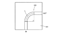
図1は、実施の形態1にかかるレーザ光源の構成を示す平面図である。このレーザ光源100は、基板101と、基板101上に形成する光導波路103と、基板101上に配置(搭載)される光学素子とを有する。光学素子は、IR光を出射するレーザ素子102と、光波長の変換をおこなう波長変換素子104と、を有する。波長変換素子104は、基板に対して水平方向に分極反転が形成されたx−Cutあるいはy−Cutの周期分極ニオブ酸リチウム(PPLN)基板からなる。(Embodiment 1)
(Configuration of laser light source)
FIG. 1 is a plan view showing the configuration of the laser light source according to the first embodiment. The
基板101は、たとえばシリコン(Si)等の半導体材質や金属、樹脂等によりなり、表面には、たとえば窒化シリコン(SiN)等の材質からなる光導波路103が設けられる。この光導波路103は、エッチング等により基板上にリッジ部を有して形成される。この光導波路103は、リッジ型に限らず、プロトン交換法により形成することもできる。
The
レーザ素子102の出射位置には、波長変換素子104の一端(入射端)が位置決めして設けられる。レーザ素子102から出射される光は、直接結合により効率よく波長変換素子104に光結合され、波長変換素子104に入射させることができる。なお、不図示であるが、レーザ素子102および波長変換素子104等の光学素子は、基板101側に設けた電極表面に微細な突起(マイクロバンプ)を形成しておき、光学素子側の電極を接合させる表面活性化の常温接合法により搭載される。
One end (incident end) of the
レーザ素子102は、たとえば、IR(赤外域)の基本波(1060nm帯)を出射し、波長変換素子104により、2次高調波(530nm帯)の緑色レーザ光(G波長)に変換した変換波を出射する。波長変換素子104の出射光は、光導波路103の一端部(光入射側)103aに入射される。これにより、波長変換素子104の出射光は、直接結合により効率よく光導波路103に光結合され、光導波路103に入射させることができる。この波長変換素子104は、変換波の波長成分に加えて、レーザ素子102が出射した基本波の成分を含み、出射する。
The
波長変換素子104としては、QPM(Quasi Phase Matching)型素子を用いることができる。特に、SHG(Second Harmonic Generation)を発生するように設計したQPM型のSHG素子である場合、SHGレーザ光源を構成できる。そして、レーザ素子102と波長変換素子104とを直接結合させ、また、波長変換素子104と光導波路103とを直接結合できるようになるため、低コスト化と、小型化が達成できる。
As the
光導波路103は、一端部103aから入射した光を内部に閉じこめ導波し、他端部103bから出射する。そして、この光導波路103の途中位置には、導波する光の進行方向を変える方向変更部113が設けられている。
The
方向変更部113は、この実施の形態1では、一端部103aに対し、他端部103bを平面上で90度曲げた方向に位置させている。この方向変更部113は、光導波路103自体を曲げた曲がり部により形成するほかに、直線の導波路の角部にミラーを設けて形成することができる。
In the first embodiment, the
図1に示すように、方向変更部113を光導波路103自体を曲げた曲がり部により形成する場合、両端の直線部の途中に曲がり部を設けてなる。この曲がり部は、できるだけ曲率を小さく、かつ、変換波の伝播損失が最小になるように決めるため、長波長側である基本波の一部を、放射モードおよびクラッドモードと結合させることにより遮断するフィルタ機能を有する。方向変更部113として曲がり部を設けた場合の光導波路103の光出力Poutは、
Pout=Pin・exp(−Σαi・li)
で表される。As shown in FIG. 1, when the
Pout = Pin · exp (−Σαi · li)
It is represented by
αiは、i番目の曲率を有する光導波路103の見かけ上の吸収係数で、曲率半径Rの関数であり、光損失の波長特性に寄与する。すなわち、除去したい基本波および透過させたい変換波の波長に応じて曲率半径Rが設定される。また、liは、i番目の曲率を有する光導波路103の導波路長であり、光損失量に寄与する。図1には、曲がり部の個数iが一つだけとしたが、曲がり部の個数iを複数設けることにより、さらに基本波の遮断効果を高めることができる。
αi is an apparent absorption coefficient of the
図2は、方向変更部として波長依存性を有するミラーを用いた構成例を示す図である。光導波路103は、一端部103a側の直線部103Aと、他端部103b側の直線部103Bからなり、これら一対の直線部103A,103Bは、互いに90度の角度を有している。これにより、90度のベント部を形成できる。そして、直線部103A,103Bが接合する角部には、所定角度θを有して異方性媒質を用いた全反射のミラー201を設ける。
FIG. 2 is a diagram illustrating a configuration example using a wavelength-dependent mirror as the direction changing unit. The
このミラー201は、所定角度θを調整することにより、直線部103Aを導波する基本波λ1(1064nm帯)の光をミラーに続く導波路の放射モードおよびクラッドモードと結合することでコア部での伝播モードを減衰させ、変換波λ2(530nm帯)の光を高効率で反射し、ミラーに続く変換波λ2の基本導波モードに高効率に結合させる。
This
図3は、ミラーの波長と反射率との関係を示す図である。ここで、ミラー201の反射光の波長依存性について検討する。MgOを5モル%ドープしたLNの反射係数ne、noを用いて計算すると、LNの異方性のためRGBの各波長での反射角は図3に表される。この演算結果によれば、B波長(470nm)では42.59度となり、G波長(530m)では42.69度となり、R波長(640nm)では42.80度が求められる。
FIG. 3 is a diagram showing the relationship between the wavelength of the mirror and the reflectance. Here, the wavelength dependence of the reflected light of the
次に、反射ミラーの調整について説明する。前記の演算の結果、たとえば、470nmの波長において、反射角は約42.6度となる。したがって、入射波と反射波とのなす角は、45+42.6=87.6度と90度より小さくなる。そのため、90度ベンドを形成するためには、ミラー201の角度を調整する必要がある。
Next, the adjustment of the reflection mirror will be described. As a result of the above calculation, for example, at a wavelength of 470 nm, the reflection angle is about 42.6 degrees. Therefore, the angle formed by the incident wave and the reflected wave is 45 + 42.6 = 87.6 degrees, which is smaller than 90 degrees. Therefore, in order to form a 90 degree bend, it is necessary to adjust the angle of the
図4は、波長とミラー角度との関係の一例を示す図である。この例によれば、ミラー角度はB波長(470nm)では43.74度となり、G波長(530nm)では43.80度となり、R波長(640nm)では43.86度が求められる。したがって、入射波が平面波で近似できるときは、ミラー201の角度を上記のように決めれば、90度ベンドが可能なことが分かる。ここで、所定の変換波長に最適化されたミラー角度は、基本波における屈折率から決まる最適角度と異なるためミラー部後の導波路において、基本波の一部は放射モードおよびクラッドモードと結合するため減衰させることができる。
FIG. 4 is a diagram illustrating an example of the relationship between the wavelength and the mirror angle. According to this example, the mirror angle is 43.74 degrees at the B wavelength (470 nm), 43.80 degrees at the G wavelength (530 nm), and 43.86 degrees at the R wavelength (640 nm). Therefore, when the incident wave can be approximated by a plane wave, it can be seen that 90 ° bend is possible if the angle of the
そして、リッジ型の光導波路103に全反射のミラー201を必要な波長に対応した角度を有して傾けて設けることにより、小さいロスで半導体レーザからの出射光を90度に曲げることができる。また、90度ベンド型のミラー201を備えた光導波路103を設けることにより、レーザ光源100全体の大きさを小型化することが可能となる。
By providing the
方向変更部113としては、上記説明のミラー201として、基本波を透過させ、変換波を反射させる特性を有する波長膜を有するハーフミラーを用いる構成とすることもできる。このミラー201においても、設置スペースを取らずに不要な基本波を遮断することができる。
As the
以上説明した実施の形態1によれば、光導波路に方向変更部を設けることにより、レーザ光源が出射し、波長変換素子により除去されなかった不要な基本波の成分を遮断し、光導波路の他端部から外部に出力することを防止できる。これにより、付加的なフィルタ素子を新たに設けなくても、所望の波長のみを外部出力できるようになる。また、光導波路に方向変更部を設けることにより、レーザ光源の小型化、特に、図1記載の縦(Y軸)方向の高さを小さくできる。 According to the first embodiment described above, by providing the direction changing portion in the optical waveguide, the laser light source emits, and unnecessary fundamental wave components that have not been removed by the wavelength conversion element are blocked. Output from the end to the outside can be prevented. Thereby, only a desired wavelength can be output to the outside without newly providing an additional filter element. Further, by providing the direction changing portion in the optical waveguide, it is possible to reduce the size of the laser light source, in particular, to reduce the height in the longitudinal (Y-axis) direction shown in FIG.
(実施の形態2)
図5は、実施の形態2にかかるレーザ光源の構成を示す平面図である。実施の形態2は、実施の形態1の変形例であり、光導波路103に2箇所の方向変更部113,113を設け、180度折り返す構成としたものである。(Embodiment 2)
FIG. 5 is a plan view showing the configuration of the laser light source according to the second embodiment. The second embodiment is a modification of the first embodiment, in which two
光導波路103は、一端部103aが波長変換素子104の出射光に直接結合され、他端部103bから外部には波長変換後の変換波が出力される。そして、2箇所の方向変更部113,113の間には、所定の長さの直線部103Cが設けられる。
One
このように、実施の形態2によれば、方向変更部を2箇所設けることにより、基本波の遮断効果をより高めることができるようになる。また、方向変更部を複数設けることにより、設けた数に応じて90度単位で任意の方向に光を外部出力できるようになる。 Thus, according to the second embodiment, the fundamental wave blocking effect can be further enhanced by providing two direction changing portions. Further, by providing a plurality of direction changing units, it is possible to output light in an arbitrary direction in units of 90 degrees according to the number provided.
(実施の形態3)
図6は、実施の形態3にかかるレーザ光源の構成を示す平面図である。実施の形態3では、R,G,B用のIR光を出射するレーザ素子102(102a〜102c)と、レーザ素子102のレーザ光(基本波)をそれぞれRGB光に波長変換して出射する複数の波長変換素子104(104a〜104c)と、光検出器(PD)105が設けられている。(Embodiment 3)
FIG. 6 is a plan view showing the configuration of the laser light source according to the third embodiment. In the third embodiment, a laser element 102 (102a to 102c) that emits IR light for R, G, and B, and a plurality of laser lights (fundamental waves) of the
基板101上の光導波路103は、一端部103a(103aa〜103ac)が各波長変換素子104(104a〜104c)の光出射端に位置し、直接結合される。他端部103baについては、光検出器105aの光入射端に位置し、他端部103bbは、光検出器105bの光入射端に位置し、他端部103bcは、外部出力される。
One
この光導波路103は、途中位置に方向変更部113と、方向性結合器123(123a,123b)が設けられている。方向変更部113は、波長変換素子104a〜104cによるR,G,B光から基本波を除去する。方向変更部113は、実施の形態1で説明したように、光導波路103自体に曲がり部を形成する方法、全反射のミラー201を設ける方法等で構成できる。
The
また、方向性結合器123a,123bは、それぞれ所定の結合長を有する。方向性結合器123aでは、R,B光を合波出力し、方向性結合器123bでは、方向性結合器123aで結合後のRB光と、G光とを合波出力する。
The
これにより、光検出器105aは、RB光レベルを検出する。また、光検出器105bは、RGB光レベルを検出する。この実施の形態3では、レーザ素子102a〜102cがいずれもIR光を出射し、波長変換素子104a〜104cによりそれぞれRGBの変換波を出射する構成とした。これに限らず、たとえば、G用のレーザ素子102bだけがIRレーザ素子であり、他のRB用のレーザ素子102a,102cは、直接発光のレーザ素子を用いる構成としてもよい。
Thereby, the
このように、複数の波長の光を出射する実施の形態3の構成においても、RGB光の光導波路103部分に方向変更部113を設けることにより、レーザ素子102(102a〜102c)が出射する基本波を遮断し、所望するRGB光だけを出射させることができるようになる。また、図6に示すように、光導波路103に対して3箇所に設ける方向変更部113は、いずれも同様の方向に向いて90度曲げられており、図6に示す横(X軸)方向の長さを縦(Y軸)方向に折り曲げているため、横方向の長さを短くすることができる。
As described above, in the configuration of the third embodiment that emits light having a plurality of wavelengths, the laser element 102 (102a to 102c) emits light by providing the
したがって、実施の形態3によれば、実施の形態1と同様に、レーザ光源が出射し、波長変換素子により除去されなかった不要な基本波の成分を遮断し、光導波路の他端部から外部に出力することを防止できる。これにより、付加的なフィルタ素子を新たに設けなくても、所望の波長のみを外部出力できるようになる。また、光導波路に方向変更部を設けることにより、基板のスペースを有効に利用でき、レーザ光源全体を小型化できるようになる。 Therefore, according to the third embodiment, similarly to the first embodiment, the laser light source emits light, blocks unnecessary fundamental wave components that are not removed by the wavelength conversion element, and is externally connected from the other end of the optical waveguide. Can be prevented from being output. Thereby, only a desired wavelength can be output to the outside without newly providing an additional filter element. Further, by providing the direction changing portion in the optical waveguide, the space of the substrate can be used effectively, and the entire laser light source can be miniaturized.
(実施の形態4)
図7は、実施の形態4にかかるレーザ光源の構成を示す平面図である。実施の形態3と同様に、R,G,B用のIR光を出射するレーザ素子102(102a〜102c)と、レーザ素子102のレーザ光(基本波)をそれぞれRGB光に波長変換して出射する複数の波長変換素子104(104a〜104c)と、光検出器(PD)105が設けられている。また、光導波路103には、2箇所に方向変更部113を設けている。(Embodiment 4)
FIG. 7 is a plan view showing a configuration of a laser light source according to the fourth embodiment. As in the third embodiment, the laser elements 102 (102a to 102c) that emit IR light for R, G, and B, and the laser light (fundamental wave) of the
光導波路103に設けた2箇所の方向変更部113,113の間には、所定の長さの直線部103cが設けられる。なお、方向変更部113を複数設けることにより、設けた数に応じて90度単位で任意の方向に光を外部出力できるようになる。図7に示す例によれば、光導波路103に対して2箇所に設けた方向変更部113は、いずれも同様の方向に向いて90度曲げられ、合計で180度折り返されている。これにより、基板101上で光導波路103の一端部103aa〜103acと同じ側に他端部103ba〜103bcを設けることができる。
A
したがって、実施の形態4によれば、方向変更部を複数設けることにより、基本波の遮断効果をより高めることができるようになる。また、光導波路に方向変更部を複数設けることにより、基板のスペースを有効に利用でき、レーザ光源全体を小型化できるようになる。 Therefore, according to the fourth embodiment, by providing a plurality of direction changing portions, the fundamental wave blocking effect can be further enhanced. Also, by providing a plurality of direction changing portions in the optical waveguide, the space of the substrate can be used effectively, and the entire laser light source can be reduced in size.
また、以上説明した各実施形態における光導波路は、基板上にエッチング等で精密に形成でき、特に、一端部と他端部の位置を精密に位置決めして設けることができる。このため、光導波路の一端部および他端部に対し、光学素子(上記各実施の形態では波長変換素子および検出器)の光入出射端を位置決めして搭載するだけで、これら光導波路と光学素子との光結合を容易、かつ低損失でおこなえるようになる。 Moreover, the optical waveguide in each embodiment described above can be precisely formed on the substrate by etching or the like, and in particular, the positions of one end and the other end can be precisely positioned. For this reason, the optical waveguide and the optical waveguide can be optically integrated only by positioning and mounting the light input / output end of the optical element (the wavelength conversion element and the detector in each of the above embodiments) with respect to one end and the other end of the optical waveguide. Optical coupling with the element can be performed easily and with low loss.
(1.ベンド構造の最適化について)
次に、導波路材料としてニオブ酸リチウムを用いた場合の曲がり導波路の曲がり部分(ベンド)構造の最適化例について説明する。
1)90度のベンド部分の長さを最適化した場合
図8は、導波路の構造を示す断面図である。基板101はニオブ酸リチウム(LN)基板であり、この基板101上に導波路103を設ける。導波路103は、ITO層801を0.27μmの厚さを有して設ける。このITO層801上にSiO2層802を1.0μmの厚さを有して設ける。SiO2層802の上にMgOを5%ドープしたLN層803を1.88μmの厚さを有して設ける。このLN層803の上にリッジ層804を1.82μmの厚さ、および幅4.7μmを有して設ける。このリッジ層804は、波長532nmに対する屈折率2.227、波長1064nmに対する屈折率2.146を有する。上記構成の導波路103のSiO2層802は、クラッド層として機能する。ITO層801は、LN部を周期分極反転構造を作成する際に使用した共通電極である。(1. Optimization of bend structure)
Next, an optimization example of the bent portion (bend) structure of the bent waveguide when lithium niobate is used as the waveguide material will be described.
1) When the length of a bend portion of 90 degrees is optimized FIG. 8 is a cross-sectional view showing the structure of a waveguide. The
図8に示す断面構造を有する導波路103を90度ベンドになるように形成することを考える。ここで、所定のSH波の波長(ここではSH波の波長532nm、基本波の波長1064nmとする)532nmで損失が最小となるときの長さLを求めるシミュレーションを行った。
Consider the formation of a
図9は、導波路のベンド部の平面図である。長さLは、導波路103のセンター位置で測った距離である。また曲率は一定とした。シミュレーションには、Photon Design社のFIMMWAVEを用いた。導波路103の両端部のOUT/INが100%に近づく最適な解の一つは、L=1248μmと求められた。このときのOUT/INのパワー比は97.3%であった。一方、同じ導波路103に1064nmの波長の光を通したときのOUT/INのパワー比は、71.5%であった。同じセクションを2段設けることで、51.1%程度まで基本波を減衰させることが可能と予測される。
FIG. 9 is a plan view of the bend portion of the waveguide. The length L is a distance measured at the center position of the
2)10度毎に曲げて各セクションの長さを最適化した場合
図10は、導波路のベンド部をサブセクションに分割する場合の平面図である。この図では、曲率半径が一定になるように見えるが、最適化計算後は各サブセクションb1〜bnの長さが異なるため、各サブセクションb1〜bnのベンド角が一定条件の場合、各サブセクションb1〜bn毎に曲率半径が異なることになる。2) When the length of each section is optimized by bending every 10 degrees FIG. 10 is a plan view when the bend portion of the waveguide is divided into subsections. In this figure, the radius of curvature seems to be constant. However, since the lengths of the subsections b1 to bn are different after the optimization calculation, each subsection b1 to bn has a constant bend angle. The radius of curvature is different for each of the sections b1 to bn.
そして、ベンド部分のベンド角を一定としていくつかのセクションに分け、所定の波長で入出力比が最大となるときの各サブセクションb1〜bnの長さを最適化するシミュレーションを行った。一例として、9サブセクション(b1〜b9)に分け、各サブセクションb1〜b9のベンド角が10度の場合の長さ(μm)結果を下記の表1に示す。ここで、各サブセクションb1〜b9の長さが異なるため、同じベンド角とするためには、各サブセクションb1〜b9の曲率半径が異なることになる。 Then, the bend angle of the bend portion was made constant and divided into several sections, and a simulation was performed to optimize the length of each of the subsections b1 to bn when the input / output ratio becomes maximum at a predetermined wavelength. As an example, Table 1 below shows the length (μm) results when the subsections b1 to b9 are divided into 9 subsections (b1 to b9) and the bend angles of the subsections b1 to b9 are 10 degrees. Here, since the lengths of the subsections b1 to b9 are different, the curvature radii of the subsections b1 to b9 are different in order to obtain the same bend angle.

表1に最適計算例を示した。このとき、532nmでのOUT/IN灯は8.5%となり、1064nmのときは75.2%となり、1)で説明した90度ベンド設計よりSH波532nmでのロスを小さくできることがわかった。また、このセクションを2段構成とした場合、1064nmでは約56.6%まで減衰可能と考えられる。 Table 1 shows an example of optimal calculation. At this time, the OUT / IN lamp at 532 nm was 8.5%, and at 1064 nm, it was 75.2%. It was found that the loss at SH wave 532 nm can be made smaller than the 90-degree bend design described in 1). Further, when this section has a two-stage configuration, it is considered that attenuation can be achieved up to about 56.6% at 1064 nm.
(2.フィルタ効果に対する考察)
上記の1)に示した構造をSHGレーザの基本波減衰フィルタに適用することを考える。実際に実用的なSHGレーザでは、PPLNで擬似位相整合が成立している場合、SH波に変換されずに漏れてくる光は、10%以下と考えられるから、たとえば上記1)の例であれば、
擬似位相整合時のPPLNへのトータル入力 150mW
SH波への変換効率 90% → 135mW
基本波の残留成分 10% → 15mW
ベンド部透過後の出力 SH波 135mW×97.3%=131.4mW
基本波 15mW×71.5%= 10.725mW
となるため、後段に簡易的なIRカットフィルタを装着するだけで、ほとんどのIR光を減衰させることが可能となる。(2. Consideration for filter effect)
Consider applying the structure shown in 1) above to a fundamental wave attenuation filter of an SHG laser. In practical SHG lasers, if pseudo phase matching is established by PPLN, the light leaking without being converted into SH waves is considered to be 10% or less. If
150mW total input to PPLN during quasi phase matching
Conversion efficiency to SH wave 90% → 135mW
Residual component of fundamental wave 10% → 15mW
Output after passing through the bend SH wave 135mW × 97.3% = 131.4mW
Fundamental wave 15mW x 71.5% = 10.725mW
Therefore, it is possible to attenuate most of the IR light only by attaching a simple IR cut filter at the subsequent stage.
上記説明では、非常に簡単なベンド構造により基本波カットフィルタを構成する例を説明した。さらに構造を工夫することで、導波路だけで十分な基本波カットフィルタを形成することが可能である。たとえば、曲がり部を多段化することにより、掛け算で基本波の減衰を大きくすることができる。 In the above description, the example in which the fundamental wave cut filter is configured with a very simple bend structure has been described. Further, by devising the structure, it is possible to form a sufficient fundamental wave cut filter with only a waveguide. For example, the attenuation of the fundamental wave can be increased by multiplying the bent portion in multiple stages.
また、曲がり部を設けることによって、当該箇所での導波路の配線を工夫すれば、導波路のピッチを変更して狭くすることも可能となり、配線領域を有効に利用できるなどの副次的な効果も生じるため、小型化にも寄与するものである。なお、形成する導波路は、Siプラットフォーム基板上に、リッジ導波路がSiプラットフォーム側に空隙またはクラッド層を介してフェースダウン構造で形成しても良い。 In addition, if the waveguide wiring is devised by providing a bent portion, the waveguide pitch can be changed and narrowed, and the wiring area can be used effectively. Since an effect also arises, it contributes also to size reduction. The waveguide to be formed may be formed on the Si platform substrate with the ridge waveguide having a face-down structure on the Si platform side via a gap or a cladding layer.
以上のように、本発明にかかるレーザ光源は、レーザ素子と、導波路と、波長変換素子等の光学素子を介して光を出射するレーザ光源に有用であり、特に、光通信システムにおける光源に適している。 As described above, the laser light source according to the present invention is useful for a laser light source that emits light through an optical element such as a laser element, a waveguide, and a wavelength conversion element. Is suitable.
100 レーザ光源
101 基板
102(102a〜102c) レーザ素子
103 光導波路
104(104a〜104c) 波長変換素子
105(105a,105b) 光検出器
113 方向変更部
123a,123b 方向性結合器DESCRIPTION OF
Claims (5)
前記レーザ素子から出射された基本波を波長変換し、変換波を出射する波長変換素子と、
前記波長変換素子の出射光を導波する導波路と、を備え、
前記導波路は、導波する光の進行方向を変える方向変更部を有し、
前記方向変更部は、前記変換波のみ通過させ、前記基本波は通過させないフィルタ機能を有する
ことを特徴とするレーザ光源。A laser element emitting a fundamental wave;
A wavelength conversion element that converts the wavelength of the fundamental wave emitted from the laser element and emits the converted wave;
A waveguide for guiding the emitted light of the wavelength conversion element,
The waveguide has a direction changing unit that changes a traveling direction of the guided light,
The direction change unit has a filter function of allowing only the converted wave to pass and not allowing the fundamental wave to pass.
前記導波路の一部を、前記基本波と前記変換波の波長に応じて所定の曲率で曲げた曲がり部からなる
ことを特徴とする請求項1に記載のレーザ光源。The direction changing unit is
2. The laser light source according to claim 1, wherein the laser light source includes a bent portion obtained by bending a part of the waveguide with a predetermined curvature in accordance with wavelengths of the fundamental wave and the converted wave.
前記導波路を互いにほぼ90度の角度を有して設けた一対の直線部と、
前記一対の直線部が接合する箇所に前記変換波の波長に応じて所定角度を有して設けたミラーと、によりなる
ことを特徴とする請求項1に記載のレーザ光源。The direction changing unit is
A pair of straight portions provided with the waveguides at an angle of approximately 90 degrees to each other;
The laser light source according to claim 1, comprising: a mirror provided with a predetermined angle in accordance with a wavelength of the converted wave at a place where the pair of linear portions are joined.
前記導波路には、複数の前記波長変換素子の出射光を光結合させる方向性結合器を備えた
ことを特徴とする請求項1〜3のいずれか一つに記載のレーザ光源。A plurality of the laser element and the wavelength conversion element,
The laser light source according to any one of claims 1 to 3, wherein the waveguide includes a directional coupler that optically couples light emitted from the plurality of wavelength conversion elements.
前記導波路の前記方向変更部は、前記基板上に複数箇所設けられた
ことを特徴とする請求項1〜4のいずれか一つに記載のレーザ光源。The waveguide is formed on a substrate;
The laser light source according to any one of claims 1 to 4, wherein a plurality of the direction changing portions of the waveguide are provided on the substrate.
Priority Applications (1)
| Application Number | Priority Date | Filing Date | Title |
|---|---|---|---|
| JP2013542932A JPWO2013069497A1 (en) | 2011-11-07 | 2012-10-29 | Laser light source |
Applications Claiming Priority (3)
| Application Number | Priority Date | Filing Date | Title |
|---|---|---|---|
| JP2011243958 | 2011-11-07 | ||
| JP2011243958 | 2011-11-07 | ||
| JP2013542932A JPWO2013069497A1 (en) | 2011-11-07 | 2012-10-29 | Laser light source |
Publications (1)
| Publication Number | Publication Date |
|---|---|
| JPWO2013069497A1 true JPWO2013069497A1 (en) | 2015-04-02 |
Family
ID=48289875
Family Applications (1)
| Application Number | Title | Priority Date | Filing Date |
|---|---|---|---|
| JP2013542932A Pending JPWO2013069497A1 (en) | 2011-11-07 | 2012-10-29 | Laser light source |
Country Status (4)
| Country | Link |
|---|---|
| US (1) | US9240671B2 (en) |
| JP (1) | JPWO2013069497A1 (en) |
| CN (1) | CN103917915B (en) |
| WO (1) | WO2013069497A1 (en) |
Families Citing this family (9)
| Publication number | Priority date | Publication date | Assignee | Title |
|---|---|---|---|---|
| JP6157911B2 (en) * | 2013-04-17 | 2017-07-05 | 富士通株式会社 | Optical semiconductor device |
| CN106461862B (en) | 2014-05-09 | 2021-08-06 | 国立大学法人福井大学 | Multiplexer, image projection device and image projection system using the same |
| US10408999B2 (en) | 2014-05-09 | 2019-09-10 | National University Corporation University Of Fukui | Multiplexer |
| JP6601662B2 (en) * | 2015-07-13 | 2019-11-06 | 富士通株式会社 | Single photon generator |
| WO2020181938A1 (en) * | 2019-03-14 | 2020-09-17 | 青岛海信宽带多媒体技术有限公司 | Optical module |
| JP7436881B2 (en) * | 2019-07-09 | 2024-02-22 | 日本電信電話株式会社 | optical multiplexing circuit |
| US11768342B2 (en) * | 2020-05-18 | 2023-09-26 | Nippon Telegraph And Telephone Corporation | Optical multiplexing circuit and optical source |
| CN114724000B (en) * | 2022-06-09 | 2022-08-30 | 深圳精智达技术股份有限公司 | Screen shot image moire processing method, device and equipment |
| DE102023114245A1 (en) * | 2023-05-31 | 2024-12-05 | Ams-Osram International Gmbh | optoelectronic semiconductor module |
Family Cites Families (22)
| Publication number | Priority date | Publication date | Assignee | Title |
|---|---|---|---|---|
| US3586872A (en) * | 1969-04-21 | 1971-06-22 | Bell Telephone Labor Inc | Apparatus including a thin film waveguide for nonlinear interaction of optical waves |
| US5109462A (en) * | 1989-09-07 | 1992-04-28 | Sharp Kabushiki Kaisha | Light wavelength converter |
| US5224193A (en) * | 1990-09-20 | 1993-06-29 | International Business Machines Corporation | First order mode frequency doubler system and method |
| WO1994016345A1 (en) * | 1993-01-08 | 1994-07-21 | Massachusetts Institute Of Technology | Low-loss optical and optoelectronic integrated circuits |
| US5544268A (en) * | 1994-09-09 | 1996-08-06 | Deacon Research | Display panel with electrically-controlled waveguide-routing |
| DE19503929A1 (en) * | 1995-02-07 | 1996-08-08 | Ldt Gmbh & Co | Color imaging systems |
| JPH10301151A (en) * | 1997-04-28 | 1998-11-13 | Nec Corp | Wavelength converter |
| JP2868084B2 (en) * | 1997-05-23 | 1999-03-10 | 日本電気株式会社 | Wavelength converter |
| US6134372A (en) * | 1997-10-01 | 2000-10-17 | Sumitomo Osaka Cement Co., Ltd. | Light intensity attenuator and attenuating method |
| US6437905B1 (en) * | 2000-07-07 | 2002-08-20 | Lucent Technologies Inc. | Optical wavelength converter |
| US6972894B2 (en) * | 2000-08-11 | 2005-12-06 | Crystal Fibre A/S | Optical wavelength converter |
| US6829080B2 (en) * | 2001-04-17 | 2004-12-07 | Matsushita Electric Industrial Co., Ltd. | Optical waveguide device and light source and optical apparatus using the same |
| JP4660999B2 (en) * | 2001-08-01 | 2011-03-30 | パナソニック株式会社 | Optical waveguide device, coherent light source and optical apparatus |
| US7403549B2 (en) * | 2003-10-01 | 2008-07-22 | Mitsubishi Denki Kabushiki Kaisha | Wavelength conversion laser and image display |
| US7865048B2 (en) * | 2006-12-28 | 2011-01-04 | Wisconsin Alumni Research Foundation | Nested waveguides |
| US7630419B2 (en) | 2007-01-10 | 2009-12-08 | Seiko Epson Corporation | Laser light source device, and image device using the same |
| US7394841B1 (en) * | 2007-01-18 | 2008-07-01 | Epicrystals Oy | Light emitting device for visual applications |
| JP2009259914A (en) | 2008-04-14 | 2009-11-05 | Sony Corp | Laser device, laser display, and laser irradiation device |
| JP2010151973A (en) * | 2008-12-24 | 2010-07-08 | Fujitsu Ltd | Optical semiconductor device, manufacturing method thereof, and optical transmission device |
| US8280211B1 (en) * | 2009-01-16 | 2012-10-02 | University Of Washington | All-optical high bandwidth sampling device based on a third-order optical nonlinearity |
| WO2010137661A1 (en) * | 2009-05-28 | 2010-12-02 | シチズンホールディングス株式会社 | Light source device |
| JP2011109002A (en) * | 2009-11-20 | 2011-06-02 | Citizen Holdings Co Ltd | Integrated device and manufacturing method therefor |
-
2012
- 2012-10-29 JP JP2013542932A patent/JPWO2013069497A1/en active Pending
- 2012-10-29 WO PCT/JP2012/077926 patent/WO2013069497A1/en not_active Ceased
- 2012-10-29 US US14/351,265 patent/US9240671B2/en not_active Expired - Fee Related
- 2012-10-29 CN CN201280054481.3A patent/CN103917915B/en not_active Expired - Fee Related
Also Published As
| Publication number | Publication date |
|---|---|
| US9240671B2 (en) | 2016-01-19 |
| CN103917915B (en) | 2016-09-21 |
| US20140293402A1 (en) | 2014-10-02 |
| CN103917915A (en) | 2014-07-09 |
| WO2013069497A1 (en) | 2013-05-16 |
Similar Documents
| Publication | Publication Date | Title |
|---|---|---|
| CN103917915B (en) | Laser light source | |
| JP5294283B2 (en) | Light source device | |
| US7171094B2 (en) | Optical waveguide device, optical waveguide laser using the same and optical apparatus equipped with the same | |
| CN108700706B (en) | Optical multiplexer circuit | |
| CN214795475U (en) | Optical waveguide element, optical modulation device using the same, and optical transmission device | |
| US9312655B2 (en) | Planar waveguide laser pumping module and planar waveguide wavelength conversion laser device | |
| JP2014222331A (en) | Wavelength conversion element | |
| WO2015152061A1 (en) | Optical modulator | |
| JP5421230B2 (en) | Wavelength conversion device and wavelength conversion device | |
| JP6232751B2 (en) | Light modulator | |
| US12204148B2 (en) | Optical connecting device, optical device, and method for manufacturing optical device | |
| JP2011064895A (en) | Wavelength conversion device and wavelength conversion apparatus | |
| JP5814183B2 (en) | Wavelength conversion device | |
| JPH11167032A (en) | Bent optical waveguide circuit | |
| JP2013127545A (en) | Semiconductor wavelength conversion element and infrared oscillation light source | |
| JP2008209522A (en) | Wavelength conversion element and wavelength conversion module | |
| WO2014199831A1 (en) | Optical path conversion element, connection structure for optical path conversion element, light source device, and optical mounting device | |
| CN220289896U (en) | Quartz substrate lithium niobate spot-size converter | |
| JP2021135367A (en) | Optical device, and light source module using the same | |
| JP6478907B2 (en) | Edge-Coupled Silicon Optical Integrated Circuit | |
| JP2006330661A (en) | Optical wavelength conversion element and optical wavelength converter | |
| KR20030042565A (en) | Optical semiconductor with curved optical waveguide | |
| JPH0373905A (en) | Optical functional element | |
| JP2008051828A (en) | Waveguide-type beam parameter product control optical circuit and optical integrated circuit | |
| JP2007322695A (en) | Wavelength conversion element |