JP2014222331A - Wavelength conversion element - Google Patents
Wavelength conversion element Download PDFInfo
- Publication number
- JP2014222331A JP2014222331A JP2013102421A JP2013102421A JP2014222331A JP 2014222331 A JP2014222331 A JP 2014222331A JP 2013102421 A JP2013102421 A JP 2013102421A JP 2013102421 A JP2013102421 A JP 2013102421A JP 2014222331 A JP2014222331 A JP 2014222331A
- Authority
- JP
- Japan
- Prior art keywords
- waveguide
- wavelength conversion
- conversion element
- base substrate
- curved
- Prior art date
- Legal status (The legal status is an assumption and is not a legal conclusion. Google has not performed a legal analysis and makes no representation as to the accuracy of the status listed.)
- Pending
Links
Images


Landscapes
- Optical Modulation, Optical Deflection, Nonlinear Optics, Optical Demodulation, Optical Logic Elements (AREA)
Abstract
【課題】本発明は効果的な導波路長の長尺化により波長変換効率の向上可能な波長変換素子を提供することを目的とする。【解決手段】本発明の波長変換素子は、ベース基板上に設けられた二次の非線形光学材料からなる三次元光導波路を備え、三次元光導波路は、周期分極反転構造が施された複数の直線導波路と、複数の直線導波路のうちの2つの直線導波路を結合する、周期分極反転構造が施されていない曲線導波路とを含み、直線導波路はベース基板における周期分極反転構造を形成できる方向と平行になるように設けられ、曲線導波路は、2つの直線導波路を導波する光の位相が整合するように長さが調整され、ベース基板は導波路の屈折率より0.75%以上低い屈折率を有するクラッド領域を含み、光導波路とベース基板のクラッド領域とが直接接合によって接合され、曲線導波路の曲率半径が0.2mm以上5mm以下である。【選択図】図2An object of the present invention is to provide a wavelength conversion element capable of improving wavelength conversion efficiency by effectively increasing the length of a waveguide. A wavelength conversion element according to the present invention includes a three-dimensional optical waveguide made of a second-order nonlinear optical material provided on a base substrate, and the three-dimensional optical waveguide includes a plurality of periodic polarization inversion structures. The linear waveguide includes a linear waveguide and a curved waveguide that is coupled with two linear waveguides of the plurality of linear waveguides and is not provided with the periodic polarization inversion structure. The linear waveguide has a periodic polarization inversion structure in the base substrate. The curved waveguide is provided so as to be parallel to the direction in which it can be formed, the length of the curved waveguide is adjusted so that the phases of the light guided through the two linear waveguides are matched, and the base substrate is zero based on the refractive index of the waveguide. Including a cladding region having a refractive index lower by .75% or more, the optical waveguide and the cladding region of the base substrate are joined by direct joining, and the radius of curvature of the curved waveguide is 0.2 mm or more and 5 mm or less. [Selection] Figure 2
Description
本発明は、波長変換素子に関し、より詳細には曲げ導波路を利用した波長変換素子に関する。 The present invention relates to a wavelength conversion element, and more particularly to a wavelength conversion element using a bent waveguide.
光通信における光信号波長変換、光変調、光計測、光加工、医療、生物工学などの応用のための紫外域−可視域−赤外域−テラヘルツ域にわたるコヒーレント光の発生と変調のために、多くの非線形光学デバイス及び電気光学デバイスの開発が進められている。このような素子に用いられる非線形光学媒質および電気光学媒質として、種々の材料が研究開発されている。ニオブ酸リチウム(LiNbO3、以下、LNという)などの酸化物系化合物基板は、2次非線形光学定数・電気光学定数が非常に高く有望な材料として知られている。LNの高い非線形性を用いた光デバイスの一例として、擬似位相整合による差周波発生を利用した波長変換素子が知られている。 Many for the generation and modulation of coherent light in the ultraviolet, visible, infrared, and terahertz range for applications such as optical signal wavelength conversion, optical modulation, optical measurement, optical processing, medicine, and biotechnology in optical communications Development of non-linear optical devices and electro-optical devices is underway. Various materials have been researched and developed as nonlinear optical media and electro-optical media used in such elements. An oxide-based compound substrate such as lithium niobate (LiNbO 3 , hereinafter referred to as LN) is known as a promising material because it has a very high second-order nonlinear optical constant / electro-optic constant. As an example of an optical device using non-linearity with high LN, a wavelength conversion element using difference frequency generation by pseudo phase matching is known.
近年、光通信システムの通信容量の増大を図るために、波長の異なる複数の光を多重化して伝送する波長分割多重(WDM)通信システムが積極的に導入されている。このようなWDM通信システムにおいては、限られた波長数を有効に利用するために、信号波長を任意の信号波長に変換する波長変換デバイスの実用化が求められている。 In recent years, in order to increase the communication capacity of an optical communication system, a wavelength division multiplexing (WDM) communication system that multiplexes and transmits a plurality of lights having different wavelengths has been actively introduced. In such a WDM communication system, in order to effectively use a limited number of wavelengths, there is a demand for practical use of a wavelength conversion device that converts a signal wavelength into an arbitrary signal wavelength.
従来、光の波長を変換する波長変換素子としては、半導体光増幅器を用いるもの、四光波混合を利用するもの等が知られている。しかしながら、これらの波長変換素子においては光通信システムにおいて求められる、高効率、高速、広帯域、低ノイズ、偏波無依存などの条件を満足させることはできていなかった。 Conventionally, as a wavelength conversion element for converting the wavelength of light, a device using a semiconductor optical amplifier, a device using four-wave mixing, and the like are known. However, these wavelength conversion elements have not been able to satisfy conditions such as high efficiency, high speed, wide band, low noise, and polarization independence required in an optical communication system.
図1に、従来のLNを用いた擬似位相整合型の波長変換素子の構成を示す。図1に示されるように、比較的小さな光強度を有する信号光Aと比較的大きな光強度を有する励起光Bとは、合波器1により合波され、分極反転構造を有する非線形光学媒質の光導波路2に入射される。光導波路2中で信号光Aは、非線形光学効果による差周波波発生により別の波長を有する変換光Cへと変換される。変換光Cは、励起光Bと共に光導波路2から出射される。出射された変換光Cと励起光Bは、分波器3により分離される。信号光A、励起光Bの波長をそれぞれλ1、λ3とすると変換光Cの波長λ2は、以下の式(1)を満たす。
1/λ2=1/λ3−1/λ1 式(1)
FIG. 1 shows a configuration of a conventional quasi phase matching type wavelength conversion element using LN. As shown in FIG. 1, the signal light A having a relatively small light intensity and the excitation light B having a relatively large light intensity are combined by a
1 / λ 2 = 1 / λ 3 -1 / λ 1 formula (1)
変換光Cの波長λ2は、信号光の波長λ1を励起光波長λ3の2倍の波長を軸に折り返した波長となる。例えば、励起光Bの波長λ3=0.78μmとした場合、波長λ1=1.54μmの信号光Aを、波長λ2=1.58μmの差周波光である変換光Cへと変換することができる。 The wavelength λ 2 of the converted light C is a wavelength obtained by turning the wavelength λ 1 of the signal light around the wavelength that is twice the wavelength of the excitation light λ 3 . For example, when the wavelength λ 3 of the excitation light B is 0.78 μm, the signal light A having a wavelength λ 1 = 1.54 μm is converted into converted light C that is a difference frequency light having a wavelength λ 2 = 1.58 μm. be able to.
信号光A及び変換光Cに対する変換帯域は、励起光の波長に対して±30nm以上と広く、例えば、波長分割多重(WDM)光通信に用いられる波長帯域C帯に束ねられたWDM信号をL帯へ、またはL帯からC帯へといった波長群の一括変換が可能である。 The conversion band for the signal light A and the converted light C is as wide as ± 30 nm or more with respect to the wavelength of the excitation light. For example, a WDM signal bundled in a wavelength band C band used for wavelength division multiplexing (WDM) optical communication is L It is possible to perform batch conversion of wavelength groups such as to the band or from the L band to the C band.
このような擬似位相整合を利用した波長変換素子を作製する従来の方法においては、LNなどの非線形光学結晶基板に周期分極反転構造を作製した後、プロトン交換導波路を作製することによって波長変換素子を作製していた。これに対して、光導波路中への光閉じ込めを改善し、バルクもしくはバルクに近い非線形効果を利用した高効率な波長変換を実現するために、リッジ型の光導波路構造を有する波長変換素子が提案されている。 In the conventional method for manufacturing a wavelength conversion element using such quasi-phase matching, a wavelength conversion element is manufactured by manufacturing a proton exchange waveguide after forming a periodically poled structure on a nonlinear optical crystal substrate such as LN. Was making. On the other hand, in order to improve the optical confinement in the optical waveguide and realize highly efficient wavelength conversion using the bulk or near-bulk nonlinear effect, a wavelength conversion element with a ridge-type optical waveguide structure is proposed Has been.
一般的なリッジ型光導波路を作製する方法を説明する。まず、Mg添加LN基板に周期分極反転構造を作製した後、別に用意したLN基板に接着剤等を用いて接着する。Mg添加LN基板の基板厚さを平面研削加工によって薄くした後、ダイシングソーを用いた精密研削加工リッジ型導波路を作製する(例えば、非特許文献1参照)。導波路作製方法としては、リソグラフィーを用いたドライエッチングプロセスを使用することもある。 A method of manufacturing a general ridge type optical waveguide will be described. First, after a periodically poled structure is fabricated on an Mg-added LN substrate, it is bonded to a separately prepared LN substrate using an adhesive or the like. After the substrate thickness of the Mg-added LN substrate is reduced by surface grinding, a precision-grinding ridge-type waveguide using a dicing saw is manufactured (for example, see Non-Patent Document 1). As a waveguide manufacturing method, a dry etching process using lithography may be used.
一方、通信波長帯における波長変換器のほか、擬似位相整合型の波長変換素子を用いて、半導体レーザで実現されていない可視域でのレーザ光源の実用化が行なわれている。現在、実用化されているレーザには、He−Neレーザ、Arレーザなどのガスレーザ、Nd:YAGレーザなどの固体レーザ、色素レーザおよび半導体レーザが知られている。近年、可視および近赤外領域の波長帯を中心に、小型・軽量、安価な半導体レーザが普及している。特に、光通信の分野では、信号光源用の1.3μm帯および1.5μm帯半導体レーザと、ファイバアンプ励起用の0.98μm帯および1.48μm帯半導体レーザとが普及している。また、光記録媒体の読取装置のピックアップ用の光源として、CD(0.78μm帯)、DVD(0.65μm帯)・ブルーレイ(0.4μm帯)の半導体レーザも普及している。 On the other hand, in addition to wavelength converters in the communication wavelength band, a laser light source in the visible range that has not been realized with a semiconductor laser has been put into practical use by using a quasi phase matching type wavelength conversion element. Currently, gas lasers such as He—Ne laser and Ar laser, solid-state lasers such as Nd: YAG laser, dye lasers and semiconductor lasers are known as lasers in practical use. In recent years, small, lightweight, and inexpensive semiconductor lasers have become widespread mainly in the visible and near-infrared wavelength bands. In particular, in the field of optical communication, 1.3 μm band and 1.5 μm band semiconductor lasers for signal light sources and 0.98 μm band and 1.48 μm band semiconductor lasers for pumping fiber amplifiers are widespread. Further, CD (0.78 μm band), DVD (0.65 μm band), and Blu-ray (0.4 μm band) semiconductor lasers are also widely used as light sources for pickup of optical recording medium readers.
しかしながら、半導体で実現することは難しい波長帯が存在することから、高効率な非線形光学媒質と広く普及している波長帯の半導体レーザを組み合わせたレーザ光源装置の開発が行われている。例えば、緑・黄緑・橙といった波長0.5〜0.6μmのレーザを、半導体で実現することは難しく、高効率な非線形光学媒質による第二高調波発生や和周波発生を用いたレーザ光源が実用化されている。 However, since there are wavelength bands that are difficult to realize with semiconductors, laser light source devices that combine highly efficient nonlinear optical media and semiconductor lasers with widely used wavelength bands have been developed. For example, it is difficult to realize a laser with a wavelength of 0.5 to 0.6 μm such as green, yellow green, and orange with a semiconductor, and a laser light source using second harmonic generation or sum frequency generation by a highly efficient nonlinear optical medium Has been put to practical use.
上述したように、様々な分野への応用が検討されている波長変換素子であるが、高機能なデバイスを実現するためには克服すべき問題が存在する。問題の一つは波長変換効率である。波長変換効率が高くなれば、第二高調波発生や和周波発生を用いたレーザ光源では出力が上がり、より高性能となる。また、差周波発生の一部であるパラメトリック増幅においては、変換効率の増加によって増幅利得の飛躍的な向上が実現できる。二次の非線形光学素子を用いた導波路型波長変換素子の変換効率ηは、以下の式(2)が成り立つことが知られている。
η∝L2/Aeff 式(2)
As described above, the wavelength conversion element is being studied for application in various fields, but there are problems to be overcome in order to realize a highly functional device. One of the problems is wavelength conversion efficiency. If the wavelength conversion efficiency increases, the output of the laser light source using the second harmonic generation or the sum frequency generation increases, and the performance becomes higher. Also, in parametric amplification, which is part of the difference frequency generation, a dramatic improvement in amplification gain can be realized by increasing the conversion efficiency. It is known that the following equation (2) holds for the conversion efficiency η of a waveguide type wavelength conversion element using a second-order nonlinear optical element.
η∝L 2 / A eff equation (2)
ここで、Lは導波路長、Aeffは導波路の有効断面積である。つまり、導波路型波長変換素子の変換効率を大きくするためには、導波路の面積を小さくし導波路長を長くすればよいことになる。導波路の面積を小さくする場合には、導波路内への光の閉じ込めを強めなくてはならないため、導波路とベース基板との間、あるいは導波路とクラッドとの間に大きな屈折率差が必要となる。 Here, L is the waveguide length, and A eff is the effective cross-sectional area of the waveguide. That is, in order to increase the conversion efficiency of the waveguide type wavelength conversion element, it is only necessary to reduce the area of the waveguide and increase the waveguide length. When reducing the area of the waveguide, it is necessary to increase the confinement of light in the waveguide, so there is a large refractive index difference between the waveguide and the base substrate, or between the waveguide and the cladding. Necessary.
しかしながら、この強い閉じ込め条件では、光のシングルモード条件及び光の伝播条件が導波路サイズの影響を受けやすい。そのため、波長変換素子として充分機能させるためには、導波路を作製する際の作製誤差を非常に小さく抑えなくてはならなくなり、面積の小型化には限界がある。現在、厚さ4μm×幅5μm程度まで小型化されているが(例えば非特許文献2参照)、厚さ2μm×幅2μm以下のサイズへのさらなる小型化は非常に困難である。 However, under this strong confinement condition, the light single mode condition and the light propagation condition are easily affected by the waveguide size. Therefore, in order to sufficiently function as a wavelength conversion element, it is necessary to suppress a manufacturing error when manufacturing a waveguide, and there is a limit to downsizing the area. Although it is currently downsized to about 4 μm thickness × 5 μm width (see, for example, Non-Patent Document 2), it is very difficult to further reduce the size to a size of 2 μm thickness × 2 μm width or less.
一方、導波路の長さ方向への拡張は、長距離に渡って均一な導波路を作製しなくてはならないものの、式(2)に示されるように変換効率ηが導波路長Lの二乗に比例するため、非常に期待されている。しかし、単純には、ウエハサイズを大きくして直線導波路として切り出せる長さを増やせばよいが、プロセス装置との適合性やウエハ全面に渡って作製誤差を小さくすることが困難といった問題がある。また、現在でも50mm程度の素子長があるが、それ以上、すなわち100mmを超えるような波長変換素子は、形状やサイズの側面においても、また素子内の温度を均一に保つ側面においても、デバイスとして利用しにくくなる。そこで、石英上のプレーナ光波回路やLN変調器で行われているような曲げ導波路を利用することが検討されている(例えば非特許文献3〜5参照)。
On the other hand, in the extension in the length direction of the waveguide, a uniform waveguide must be produced over a long distance, but the conversion efficiency η is the square of the waveguide length L as shown in Equation (2). Is highly expected. However, simply increasing the wafer size and increasing the length that can be cut out as a linear waveguide is problematic, but there are problems such as compatibility with process equipment and difficulty in reducing manufacturing errors over the entire wafer surface. . Further, there is an element length of about 50 mm at present, but a wavelength conversion element longer than that, that is, more than 100 mm, is a device in terms of shape and size as well as in terms of keeping the temperature inside the element uniform. It becomes difficult to use. Therefore, it has been studied to use a bent waveguide such as that used in a planar lightwave circuit on quartz or an LN modulator (see, for example, Non-Patent
しかしながら、周期的な分極反転構造を備えた波長変換素子に曲げ導波路構造を適応することにより、効果的な導波路の長尺化と、当該長尺化による変換効率の向上を実現した発明および作製方法は開示されていない。 However, by applying a bent waveguide structure to a wavelength conversion element having a periodic domain-inverted structure, the invention has achieved an effective lengthening of the waveguide and an improvement in conversion efficiency due to the lengthening. The manufacturing method is not disclosed.
このような目的を達成するために、請求項1に記載の波長変換素子は、ベース基板と、前記ベース基板上に設けられた二次の非線形光学材料からなる三次元光導波路とを備えた波長変換素子であって、前記三次元光導波路は、周期分極反転構造が施された複数の直線導波路と、前記複数の直線導波路のうちの2つの直線導波路を結合する、周期分極反転構造が施されていない曲線導波路とを含み、前記曲線導波路は、前記2つの直線導波路をそれぞれ導波する光の位相が整合するように長さが調整されており、前記ベース基板は前記導波路の屈折率より0.75%以上低い屈折率を有するクラッド領域を含み、前記光導波路と前記ベース基板の前記クラッド領域とが直接接合によって接合されており、前記曲線導波路の曲率半径が0.2mm以上5mm以下であることを特徴とする。
In order to achieve such an object, the wavelength conversion element according to
請求項2に記載の波長変換素子は、請求項1に記載の波長変換素子であって、前記クラッド領域を含む前記ベース基板は、LiNbO3、KNbO3、LiTaO3、LiNbxTa1-xO3(0≦x≦1)、KTiOPO4、若しくは、それらにMg、Zn、Sc、Inからなる群から選ばれた少なくとも一種を添加物として含有する材料、又は石英、酸化珪素を含む高融点材料からなることを特徴とする。
The wavelength conversion element according to
請求項3に記載の波長変換素子は、請求項1又は2に記載の波長変換素子であって、前記ベース基板は、前記ベース基板の前記クラッド領域上及び前記三次元光導波路上に、クラッド領域が更に設けられていることを特徴とする。
The wavelength conversion element according to
請求項4に記載の波長変換素子は、請求項1乃至3のいずれかに記載の波長変換素子であって、前記曲線導波路の上面、または側面、または前記ベース基板上に前記曲線導波路に沿って電極が設けられていることを特徴とする。 A wavelength conversion element according to a fourth aspect is the wavelength conversion element according to any one of the first to third aspects, wherein the curved waveguide is formed on an upper surface or a side surface of the curved waveguide or on the base substrate. The electrode is provided along.
請求項5に記載の波長変換素子は、請求項1乃至4のいずれかに記載の波長変換素子であって、前記非線形光学材料は、LiNbO3、KNbO3、LiTaO3、LiNbxTa1-xO3(0≦x≦1)、KTiOPO4、または、それらにMg、Zn、Sc、Inからなる群から選ばれた少なくとも一種を添加物として含有する材料からなることを特徴とする。
The wavelength conversion element according to
請求項6に記載の波長変換素子は、請求項1乃至5のいずれかに記載の波長変換素子であって、前記1又は複数の曲線導波路の各々は、2つの90°導波路部分からなる曲線導波路であることを特徴とする。
The wavelength conversion element according to claim 6 is the wavelength conversion element according to any one of
請求項7に記載の波長変換素子は、請求項1乃至5のいずれかに記載の波長変換素子であって、前記1又は複数の曲線導波路の各々は、60°曲線導波路及び120°曲線導波路のいずれかであることを特徴とする。
The wavelength conversion element according to claim 7 is the wavelength conversion element according to any one of
請求項8に記載の波長変換素子は、請求項1乃至7のいずれかに記載の波長変換素子であって、前記曲線導波路は、前記2つの直線導波路をそれぞれ導波する光の位相が整合するように長さが調整された直線導波路部分を含むことを特徴とする。
The wavelength conversion element according to claim 8 is the wavelength conversion element according to any one of
以上説明したように、本発明によれば、素子サイズの増大を抑えつつ、効果的な導波路長の長尺化が可能となり、それにより波長変換効率の向上を実現でき、従来に比べ著しく高性能な波長変換素子デバイスを提供することができる。 As described above, according to the present invention, it is possible to increase the effective waveguide length while suppressing an increase in the element size, thereby realizing an improvement in wavelength conversion efficiency, which is significantly higher than the conventional one. A high-performance wavelength conversion element device can be provided.
以下、図面を参照しながら、本発明に係る波長変換素子の各実施例について詳細に説明する。 Hereinafter, embodiments of the wavelength conversion element according to the present invention will be described in detail with reference to the drawings.
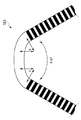
(実施例1)
図2に、本発明の実施例1に係る波長変換素子の上面図を示す。図2には、直線導波路101及び103と、直線導波路101及び103を結合する曲線導波路102とがベース基板110に設けられた波長変換素子100が示されている。直線導波路101及び103は、幅3μm、厚さ3μm、長さ50mmの周期的分極反転構造が施されたリッジ型の三次元光導波路とすることができ、曲線導波路102は、幅3μm、厚み3μmのリッジ型の三次元光導波路とすることができる。
Example 1
FIG. 2 shows a top view of the wavelength conversion element according to Example 1 of the present invention. FIG. 2 shows the
三次元光導波路とは、上下および左右方向に光を閉じ込め、長さ方向に光を伝播する導波路を意味し、リッジ型導波路はその一例である。周期的分極反転構造は直線導波路101及び103のみに施されており、曲線導波路102には施されていない。直線導波路101の入射端から入射された光は、直線導波路101及び直線導波路103で波長変換されながら、直線導波路103の出射端から出射する。
A three-dimensional optical waveguide means a waveguide that confines light vertically and horizontally and propagates light in the length direction, and a ridge-type waveguide is an example. The periodic domain-inverted structure is applied only to the
図3に、本発明に係る波長変換素子100における曲線導波路102の拡大図を示す。図3に示されるように、U字曲線形状の曲線導波路102は、直線導波路部分1021、90°導波路部分1022及び1023とから構成されている。直線導波路101は、90°導波路部分1022を介して直線導波路101の導波路方向を90°変更されて直線導波路部分1021に接続されており、直線導波路部分1021は90°導波路部分1023を介して直線導波路部分1021の導波路方向を90°変更されて直線導波路103に接続されている。90°導波路部分1022及び1023の曲率半径Rはおよそ0.5mmとし、直線導波路部分1021の直線領域S0はおよそ0.5mmとすることができる。
FIG. 3 shows an enlarged view of the
三次元導波路としては、LN結晶からなる基板を用いることができる。非線形光学材料であるLNのZ面は3回対称の結晶構造を有しているため、直線導波路101及び直線導波路103において周期分極反転構造を形成できる方向は1方向だけでなく3方向存在する。直線導波路101及び直線導波路103は、上記のように曲線導波路102を介して接続されることにより、その導波路方向がLNのZ面における周期分極反転構造を形成できる3方向のうちの1方向と平行となるように設けられている。
As the three-dimensional waveguide, a substrate made of an LN crystal can be used. Since the Z plane of LN, which is a nonlinear optical material, has a three-fold symmetric crystal structure, there are not only one direction in which the periodic polarization inversion structure can be formed in the
曲線導波路102のU字曲線部分には、周期分極反転構造が施されていないため、直線導波路101から直線導波路103に伝播する際、波長変換に関わる光同士の位相整合がとれていなければ効果的な変換が達成されない。そのため、例えば直線導波路部分1021の直線領域S0の長さを調整することによって位相の調整を行い、直線領域S0の長さを直線導波路101の導波光の位相と直線導波路103の導波光の位相とが整合する長さとすることにより、変換効率の劣化を抑制している。
Since the U-curve portion of the
一方、非特許文献3及び4に示されるように、損失無く曲げられる曲率半径Rは、導波路とクラッド領域との屈折率差に依存している。非特許文献3やBPM(Beam Propagation Method)によるシミュレーションによると、埋め込み導波路の場合は以下の式(3)〜式(7)の関係がある。
屈折率差Δ=0.75%の時、最小曲率半径Rmin≒5mm 式(3)
屈折率差Δ=1.5%の時、最小曲率半径Rmin≒2mm 式(4)
屈折率差Δ=2.5%の時、最小曲率半径Rmin≒1mm 式(5)
屈折率差Δ=5%の時、最小曲率半径Rmin≒0.8mm 式(6)
屈折率差Δ=10%の時、最小曲率半径Rmin≒0.5mm 式(7)
On the other hand, as shown in
When the refractive index difference Δ = 0.75%, the minimum radius of curvature R min ≈5 mm (3)
When the refractive index difference Δ = 1.5%, the minimum radius of curvature R min ≈2 mm (4)
When the refractive index difference Δ = 2.5%, the minimum curvature radius R min ≈1 mm (5)
When refractive index difference Δ = 5%, minimum radius of curvature R min ≈0.8 mm Equation (6)
When the refractive index difference Δ = 10%, the minimum radius of curvature R min ≈0.5 mm (7)
導波路とクラッド領域との屈折率差Δが0.75%未満である場合、曲率半径Rは5mm超となり、基板を有効に利用することができず、素子サイズが大きくなってしまう。一方、最小曲率半径Rminが0.2mmを下回るような高屈折率差の場合、導波路への閉じ込めが強すぎ、シングルモードにするためにはコアサイズを非常に小さくしなくてはならなくなる。その場合、前述したように許容される作製誤差が小さくなりすぎてしまい、現在の技術では均一な素子を作製することができず、逆に変換効率が低下する。 When the refractive index difference Δ between the waveguide and the cladding region is less than 0.75%, the radius of curvature R exceeds 5 mm, the substrate cannot be used effectively, and the element size increases. On the other hand, when the refractive index difference is high such that the minimum radius of curvature R min is less than 0.2 mm, the confinement in the waveguide is too strong, and the core size must be made very small in order to achieve single mode. . In that case, as described above, the allowable manufacturing error becomes too small, and with the current technology, a uniform element cannot be manufactured, and conversely, conversion efficiency decreases.
実施例1に係る波長変換素子100では、導波路の屈折率がおよそ2.1であり、ベース基板110のクラッド領域の屈折率差Δをおよそ10%に設定した。クラッド領域は、高融点のSiO2から構成し、その厚みを調整することで両層の実効屈折率差を調整した。導波路長を徐々に短くして導波損失を調べるカットバック法によると、90°の曲げによる損失は一個あたりおよそ−0.05dBであり、合計で−0.1dB程度であった。
In the
図4に、本発明の実施例1に係る波長変換素子100の断面図を示す。図4には、ベース基板110と、ベース基板110上に設けられた三次元光導波路120とを備えた波長変換素子100が示されている。波長変換素子100の三次元光導波路120には、非線形光学媒質であるZカットZn添加LNを用いた。ベース基板110は、ZカットMg添加LN基板111とプラズマCVD法でZカットMg添加LN基板111上に蒸着した高融点SiO2層からなるクラッド領域112により構成し、蒸着量の調整により三次元光導波路120とクラッド領域112との実効屈折率の調整が可能な構造となっている。三次元光導波路120の周辺には溝130が形成されており、三次元光導波路120の上方および左右の空気層と、三次元光導波路120の下方のクラッド領域112により効果的な光の閉じ込めが実現できるリッジ構造となっている。
FIG. 4 is a sectional view of the
クラッド領域112としては、高融点SiO2あるいは石英等の材料を用いることが望ましい。クラッド領域112として高融点の材料を用いる理由は、温度耐性のためである。入出力光の一部は、導波路に吸収されて熱に変換される。本発明は高変換効率による高性能波長変換素子を実現することを目的としているため、非常に強い入力および出力になる可能性がある。このため、クラッド領域112が低融点ガラスや接着剤からなる場合、融点が低いために、クラッド領域の屈折率が熱による温度上昇の影響を受けやすく、特性が安定しないという欠点がある。また、導波路領域のクラッド層の厚みをリソグラフィーとエッチングによって調整することもあるため、クラッド領域112としてこれらの技術に適合性がある高融点SiO2あるいは石英(水晶)等の材料を用いることが望ましい。 As the cladding region 112, it is desirable to use a material such as high melting point SiO 2 or quartz. The reason for using a high melting point material for the cladding region 112 is for temperature resistance. Part of the input / output light is absorbed by the waveguide and converted into heat. Since the present invention aims to realize a high-performance wavelength conversion element with high conversion efficiency, there is a possibility of very strong input and output. For this reason, when the cladding region 112 is made of low-melting glass or adhesive, since the melting point is low, the refractive index of the cladding region is easily affected by a temperature rise due to heat, and the characteristics are not stable. In addition, since the thickness of the cladding layer in the waveguide region may be adjusted by lithography and etching, a material such as high melting point SiO 2 or quartz (quartz) that is compatible with these techniques is used as the cladding region 112. desirable.
また、本発明に係るクラッド領域112は、高融点を有するように構成されているため、素子作製時において低融点ガラスや接着剤のような導波路層とベース基板との接合を促進する接着効果は薄く、両者を接合させる接合層としての役割はない。この点、特許文献1に開示された接着効果を有する接合層を介した光導波路素子とは異なる。
In addition, since the cladding region 112 according to the present invention is configured to have a high melting point, an adhesive effect that promotes bonding between a waveguide layer such as a low-melting glass or an adhesive and the base substrate during device fabrication. Is thin and does not serve as a bonding layer for bonding the two. In this respect, the optical waveguide element disclosed in
図5は、本発明の実施例1に係る波長変換素子の他の例を示す。図5には、ベース基板210と、三次元光導波路220と、上部クラッド領域230とを備えた波長変換素子200が示されている。波長変換素子の構造は図4に示される構造だけでなく、図5に示すように、ベース基板210全体がクラッド領域であり、また、このベース基板210のクラッド領域上及び三次元光導波路220上にさらに上部クラッド領域230が設けられたような構造としてもよい。図5に示される波長変換素子200では、ベース基板210としてZカット水晶基板を使用し、上部クラッド領域230としてスパッタ法で堆積したTa2O5を使用した。
FIG. 5 shows another example of the wavelength conversion element according to the first embodiment of the present invention. FIG. 5 shows a
図6は、本発明の実施例1に係る波長変換素子のさらに他の例を示す。図6には、LN基板311と下部クラッド領域312とからなるベース基板310と、三次元光導波路320と、上部クラッド領域330とを備えた波長変換素子300が示されている。図6に示すように、下部クラッド領域312及び上部クラッド領域330で三次元光導波路320を挟み込むように、下部クラッド領域312に対向する上部クラッド領域330を基板の直接接合により接合することもできる。図6に示される波長変換素子300では、LN基板311としてZカットMg添加LN基板を使用し、下部クラッド領域312としてプラズマCVD法で蒸着した高融点SiO2層を使用し、上部クラッド領域330としてZカット水晶基板を使用した。
FIG. 6 shows still another example of the wavelength conversion element according to the first embodiment of the present invention. FIG. 6 shows a
次に、図7を用いて本発明に係る波長変換素子の作製方法を説明する。図7(a)ではベース基板としてプラズマCVD法でSiO2を堆積したZカットMgドープLN基板を用いた例を示し、図7(b)はベース基板として水晶基板を用いた例を示す。図7において、非線形光学材料である導波路用基板にはZカットZn添加LN基板を使用することができ、予め1.5μm帯で位相整合条件が満たされるように周期分極反転構造が作製されている。また、導波路用基板には、直線導波路101及び103を構成する周期分極反転構造が形成された部分と、曲線導波路102を構成する周期分極反転構造が形成されていない部分とが作り込まれている。
Next, a method for manufacturing a wavelength conversion element according to the present invention will be described with reference to FIGS. FIG. 7A shows an example using a Z-cut Mg-doped LN substrate in which SiO 2 is deposited by plasma CVD as the base substrate, and FIG. 7B shows an example using a quartz substrate as the base substrate. In FIG. 7, a Z-cut Zn-doped LN substrate can be used as a waveguide substrate that is a nonlinear optical material, and a periodically poled structure is prepared in advance so that the phase matching condition is satisfied in the 1.5 μm band. Yes. The waveguide substrate is formed with a portion where the periodic polarization reversal structure constituting the
導波路用基板及びベース基板は熱膨張係数がほぼ一致しており、導波路用基板及びベース基板の何れも両面が光学研磨されてある3インチウエハとすることができる。導波路用基板の厚さは300μmとすることができ、ベース基板の厚さはおよそ500μmとすることができる。なお、導波路用基板の非線形光学媒質として、LNの他に、KNbO3、LiTaO3、LiNbxTa1-xO3(0≦x≦1)、KTiOPO4、または、それらにMg、Zn、Sc、Inからなる群から選ばれた少なくとも一種を添加物として含有する材料を用いることができる。また、ベース基板として、LNの他に、KNbO3、LiTaO3、LiNbxTa1-xO3(0≦x≦1)、KTiOPO4、または、それらにMg、Zn、Sc、Inからなる群から選ばれた少なくとも一種を添加物として含有する材料、石英(水晶)、酸化珪素を含む高融点材料を用いることができる。 The thermal expansion coefficients of the waveguide substrate and the base substrate are substantially the same, and both the waveguide substrate and the base substrate can be a 3-inch wafer having both surfaces optically polished. The thickness of the waveguide substrate can be 300 μm, and the thickness of the base substrate can be approximately 500 μm. In addition to LN, KNbO 3 , LiTaO 3 , LiNb x Ta 1-x O 3 (0 ≦ x ≦ 1), KTiOPO 4 , or Mg, Zn, or the like as the nonlinear optical medium of the waveguide substrate A material containing at least one selected from the group consisting of Sc and In as an additive can be used. In addition to LN, KNbO 3 , LiTaO 3 , LiNb x Ta 1-x O 3 (0 ≦ x ≦ 1), KTiOPO 4 , or a group consisting of Mg, Zn, Sc, and In is used as the base substrate. A material containing at least one selected from the above as an additive, quartz (quartz), and a high melting point material containing silicon oxide can be used.
用意した導波路用基板及びベース基板の表面を、通常の酸洗浄あるいはアルカリ洗浄によって親水性にした後、導波路用基板及びベース基板をマイクロパーティクルが極力存在しない清浄雰囲気中で重ね合わせる。そして、重ね合わせた導波路用基板及びベース基板を電気炉に入れ、400℃で3時間程度熱処理することにより、導波路用基板及びベース基板の拡散接合を行う。接合された基板は、接合面にマイクロパーティクル等の挟み込みがなく、ボイドフリーであり、室温に戻したときにおいてもクラックなどは発生しない。なお、導波路を形成する導波路用基板の接合面に高融点SiO2を適切な量蒸着して接合面の材質をそろえることにより、接合強度を高めることもできる。 After the surfaces of the prepared waveguide substrate and base substrate are made hydrophilic by normal acid cleaning or alkali cleaning, the waveguide substrate and base substrate are superposed in a clean atmosphere in which microparticles are not present as much as possible. The superposed waveguide substrate and base substrate are placed in an electric furnace and heat-treated at 400 ° C. for about 3 hours, thereby performing diffusion bonding between the waveguide substrate and the base substrate. The bonded substrate is free from microparticles and the like on the bonding surface, is void free, and does not crack when returned to room temperature. The bonding strength can also be increased by depositing an appropriate amount of high melting point SiO 2 on the bonding surface of the waveguide substrate forming the waveguide so as to align the material of the bonding surface.
次に、研磨定盤の平坦度が管理された研磨装置を用いて、接合された基板の導波路用基板部分の厚さがおよそ6μmになるまで研磨加工を施す。研磨加工の後に、さらにポリッシング加工を行うことにより、所望の基板厚みで、鏡面の研磨表面を得ることができる。 Next, using a polishing apparatus in which the flatness of the polishing platen is controlled, polishing is performed until the thickness of the waveguide substrate portion of the bonded substrate becomes approximately 6 μm. By performing a polishing process after the polishing process, a mirror-polished polishing surface can be obtained with a desired substrate thickness.
基板の平行度(最大高さと最小高さとの差)を光学的な平行度測定機を用いて測定して、3インチウエハの周囲を除き、ほぼ全体にわたってサブミクロンの平行度を得ることにより、波長変換素子の作製に好適な薄膜基板を作製することができる。この薄膜基板は、接着剤を用いずに導波路用基板とベース基板とを熱処理による拡散接合によって直接接合することにより作製したものであるため、3インチウエハの全面積にわたって均一な組成及び膜厚を有する。 By measuring the parallelism of the substrate (difference between the maximum and minimum height) using an optical parallelism measuring instrument to obtain a submicron parallelism over almost the whole area except for the periphery of the 3-inch wafer, A thin film substrate suitable for manufacturing a wavelength conversion element can be manufactured. Since this thin film substrate is produced by directly bonding a waveguide substrate and a base substrate by diffusion bonding by heat treatment without using an adhesive, it has a uniform composition and film thickness over the entire area of a 3-inch wafer. Have
その後、光導波路の作製手段としては、ドライエッチングプロセスを用いて、薄膜基板において波長変換導波路を作製する。薄膜基板のうちの導波路用基板部分の表面に通常のフォトリソグラフィのプロセスによって導波路パターンを作製する。その後、ドライエッチング装置に基板をセットし、Arガスをエッチングガスとして薄膜基板の導波路用基板の表面をエッチングすることにより、図2に示すようなリッジ型の三次元光導波路を形成して、図1に示されるような波長変換素子100を作製した。
Thereafter, as a means for producing the optical waveguide, a wavelength conversion waveguide is produced on the thin film substrate by using a dry etching process. A waveguide pattern is formed on the surface of the waveguide substrate portion of the thin film substrate by an ordinary photolithography process. Thereafter, the substrate is set in a dry etching apparatus, and the surface of the waveguide substrate of the thin film substrate is etched using Ar gas as an etching gas, thereby forming a ridge type three-dimensional optical waveguide as shown in FIG. A
波長変換デバイスとしての特性を得るために、作製した波長変換素子100の直線導波路101の入射端から1.56μm帯の信号光を入力することによって直線導波路103の出射端から出力された第二高調波により、波長変換の効率を評価した。本発明の実施例1に係る波長変換素子においては、幅3μm、厚さ3μmという小さい導波路サイズ、高屈折率差による強い閉じ込め、および合計100mmという長い波長変換領域の結果、規格化変換効率は波長1555nmの光を入力光とした場合において6000%/Wと高い値が得られた。上述のように曲線領域による損失は非常に小さかった。
In order to obtain the characteristics as a wavelength conversion device, the signal output in the 1.56 μm band is input from the incident end of the
(実施例2)
次に、図8及び図9を用いて本発明の実施例2に係る波長変換素子を説明する。図8は、本発明の実施例2に係る波長変換素子の上面図を示す。図8には、直線導波路401及び403と、直線導波路401及び403を結合する曲線導波路402とがベース基板410上に設けられた波長変換素子400が示されている。図8に示されるように、ベース基板410上には後述するバッファー層444を介して底面電極441が設けられており、曲線導波路402上にはバッファー層444を介して上部電極442及び側面電極443が設けられている。
(Example 2)
Next, a wavelength conversion element according to Example 2 of the present invention will be described with reference to FIGS. FIG. 8 is a top view of the wavelength conversion element according to the second embodiment of the present invention. FIG. 8 shows a
また、図9に、本発明の実施例2に係る波長変換素子400の断面図を示す。図4には、LN基板411及びクラッド領域412からなるベース基板410と、ベース基板410上に設けられた三次元光導波路420と、クラッド領域412及び三次元光導波路420上に設けられたバッファー層444と、バッファー層444上に三次元光導波路420に沿って設けられた底面電極441と、三次元光導波路420の上面のバッファー層444上に設けられた上部電極442と、三次元光導波路420の側面の一方のバッファー層444上に設けられた側面電極443とを備えた波長変換素子400が示されている。各電極の下には、導波領域に金属が存在することよる光の損失を回避するために、スパッタ法により堆積したおよそ0.5μm厚のSiO2をバッファー層444として形成している。
FIG. 9 shows a cross-sectional view of a
上述のように、分極反転を形成していない曲線導波路部分は位相を調整する必要がある。通常、この位相調整は曲線導波路の直線領域S0の長さを調整することで行うが、素子作製のばらつきにより設計と若干のずれが生じることがある。このずれを補正するために、図8及び図9に示すように底面電極441と上部電極442と側面電極443とを形成することができる。 As described above, it is necessary to adjust the phase of the curved waveguide portion where the polarization inversion is not formed. Normally, this phase adjustment is performed by adjusting the length of the straight region S 0 of the curved waveguide may be formed a slight shift and design by variation of the element produced. In order to correct this deviation, a bottom electrode 441, an upper electrode 442, and a side electrode 443 can be formed as shown in FIGS.
図8及び図9に示される上部電極442及び側面電極443を作製した場合、上部電極442及び側面電極443間に電流を流すことにより三次元光導波路420を加熱し、温度による屈折率変化を発生するTO効果を利用して位相のずれを補正することができる。また、上部電極442と、図8で示される底面電極441とを形成し、底面電極441と上部電極442との間に電界を印加することで電界による屈折率変化を発生するEO効果を利用して位相のずれを補正してもよい。EO効果を用いる場合は、底面電極を三次元導波路420の両側に挟み込むように形成し、両側の底面電極の電位を揃える構成にしてもよい。 When the upper electrode 442 and the side electrode 443 shown in FIGS. 8 and 9 are manufactured, the three-dimensional optical waveguide 420 is heated by passing a current between the upper electrode 442 and the side electrode 443, and a refractive index change due to temperature is generated. The phase shift can be corrected using the TO effect. Further, an EO effect is used in which an upper electrode 442 and a bottom electrode 441 shown in FIG. 8 are formed and an electric field is applied between the bottom electrode 441 and the upper electrode 442 to generate a refractive index change due to the electric field. Thus, the phase shift may be corrected. When the EO effect is used, the bottom electrode may be formed so as to be sandwiched between both sides of the three-dimensional waveguide 420 and the potentials of the bottom electrodes on both sides may be made uniform.
(実施例3)
次に、本発明の実施例3に係る波長変換素子を説明する。図10は、本発明の実施例3に係る波長変換素子の上面図を示す。図10には、直線導波路501、503及び505と、直線導波路501及び503を結合する曲線導波路502と、直線導波路503及び505を結合する曲線導波路504とがベース基板510上に設けられた波長変換素子500が示されている。
Example 3
Next, a wavelength conversion device according to Example 3 of the present invention will be described. FIG. 10 is a top view of the wavelength conversion element according to the third embodiment of the present invention. In FIG. 10, linear waveguides 501, 503, and 505, a curved waveguide 502 that couples linear waveguides 501 and 503, and a curved waveguide 504 that couples linear waveguides 503 and 505 are formed on
図10に示される波長変換素子500は、図2に示される波長変換素子100にさらに直線導波路を結合した構成であり、直線導波路501の入射端から光を入射し、直線導波路505の出射端から出射する。直線導波路501、503及び505の長さは50mmとすることができる。実施例3に係る波長変換素子500によると、実施例1に示される波長変換素子100よりも直線導波路505の長さ分だけ長さがさらに増えたことにより変換効率が増加し、規格化変換効率は波長1555nmの光を入力光とした場合において10000%/Wと高い値が得られた。長さの二乗で増加しないのは、わずかに生じる作製の不均一さのため全ての領域が変換に寄与しないためである。
A
(実施例4)
次に、本発明の実施例4に係る波長変換素子を説明する。図11は、本発明の実施例4に係る波長変換素子の上面図を示す。図11には、直線導波路602、604、606、608及び610と、直線導波路602に接続された曲線導波路601と、直線導波路602及び604を結合する曲線導波路603と、直線導波路604及び606を結合する曲線導波路605と、直線導波路606及び608を結合する曲線導波路607と、直線導波路608及び610を結合する曲線導波路609とがベース基板620上に設けられた波長変換素子600が示されている。
Example 4
Next, a wavelength conversion element according to Example 4 of the present invention will be described. FIG. 11 shows a top view of a wavelength conversion element according to Example 4 of the present invention. FIG. 11 shows
図11に示される波長変換素子600では、S字形状を有する曲線導波路601の入射端から光を入射し、直線導波路602、604、606、608、610及びこれらの直線導波路を結合するU字形状の曲線導波路603、605、607、609を介して直線導波路610の出射端から出射する。
In the
図11に示される波長変換素子600は、図10に示される波長変換素子500にさらに直線導波路を2本結合した構成を有しており、直線導波路が5本結合されている。実施例4に係る波長変換素子600は、波長変換素子600の中央部分に光の入出力端が存在し、光ファイバ等との結合に有利な形状となっている。
A
図11に示される波長変換素子600において、直線領域S1は50mmとし、入出力部分S2はおよそ0.5mmとし、非分極反転直線導波路S3、S4、S5は各々およそ1.5mm、およそ0.5mm、およそ2.5mmとし、導波路間隔Dは0.5mmとし、曲率半径Rは0.5mmとした。波長変換素子600においては、非分極反転領域において位相整合がとれるように曲線導波路の直線導波路部分の長さが調整されている。実施例4に係る波長変換素子600の規格化変換効率としては、波長1555nmの光を入力光とした場合に20000%/Wが得られた。
In the
(実施例5)
次に、本発明の実施例5に係る波長変換素子を説明する。図12は、本発明の実施例4に係る波長変換素子の上面図を示す。図12には、複数の直線導波路702と、複数の直線導波路702のうちの2つを結合する複数の120°曲線導波路701及び60°曲線導波路703とがベース基板710上に形成された波長変換素子700が示されている。図12に示されるように、波長変換素子700では、複数の直線導波路702が120°曲線導波路701又は60°曲線導波路703で結合されることにより、ベース基板710上で導波路全体が正三角形の渦巻き型形状に形成されている。
(Example 5)
Next, a wavelength conversion element according to Example 5 of the present invention will be described. FIG. 12 is a top view of the wavelength conversion element according to the fourth embodiment of the present invention. In FIG. 12, a plurality of
上述のように、非線形光学材料であるLNのZ面は3回対称の結晶構造を有しているため、周期分極反転構造を形成できる方向は1方向だけでなく3方向存在する。そこで、図12に示すような60°方向に曲がる60°曲線導波路703、あるいは120°方向に曲がる120°曲線導波路701で直線導波路702を結合することにより、図13に示すような渦巻き型の波長変換素子700の作製も可能である。実施例5に係る波長変換素子700は正三角形の3辺に対応する方向に沿って分極反転構造が形成されている。実施例5に係る渦巻き型の波長変換素子700は、基板を効率的に利用できるという利点を有する。
As described above, since the Z plane of LN, which is a nonlinear optical material, has a three-fold symmetric crystal structure, there are not only one direction but also three directions in which a periodically poled structure can be formed. Therefore, by connecting the
上述してきた本発明に係る波長変換素子によると、適切な実行屈折率差を生じる高融点のクラッド領域の採用と、直線導波路を適切な曲率半径を有する曲線導波路によって結合する構造を採用することにより、従来とほぼ等しい素子サイズで、変換効率が著しく向上した高性能な波長変換素子を実現することができる。 According to the wavelength conversion element according to the present invention described above, a high melting point cladding region that produces an appropriate effective refractive index difference and a structure in which a straight waveguide is coupled by a curved waveguide having an appropriate radius of curvature are adopted. Accordingly, it is possible to realize a high-performance wavelength conversion element having a conversion efficiency remarkably improved with an element size substantially equal to that of the prior art.
合波器 1
光導波路 2
分波器 3
波長変換素子 100、200、300、400、500、600、700
直線導波路 101、103、401、403、501、503、505、602、604、606、608、610、702
曲線導波路 102、402、502、504、601、603、605、607、609
ベース基板 110、210、310、410、510、620、710
LN基板 111、311、411
クラッド領域 112、412
三次元光導波路 120、220、320、420
溝 130、240、340
上部クラッド領域 230、330
下部クラッド領域 312
底面電極 441
上部電極 442
側面電極 443
バッファー層 444
120°曲線導波路 701
60°曲線導波路 703
LN substrate 111, 311, 411
Clad region 112, 412
Three-dimensional optical waveguide 120, 220, 320, 420
Bottom electrode 441
Upper electrode 442
Side electrode 443
Buffer layer 444
120 °
60 °
Claims (8)
前記ベース基板上に設けられた二次の非線形光学材料からなる三次元光導波路と
を備えた波長変換素子であって、
前記三次元光導波路は、周期分極反転構造が施された複数の直線導波路と、前記複数の直線導波路のうちの2つの直線導波路を結合する、周期分極反転構造が施されていない曲線導波路とを含み、
前記曲線導波路は、前記2つの直線導波路をそれぞれ導波する光の位相が整合するように長さが調整されており、
前記ベース基板は前記導波路の屈折率より0.75%以上低い屈折率を有するクラッド領域を含み、前記光導波路と前記ベース基板の前記クラッド領域とが直接接合によって接合されており、前記曲線導波路の曲率半径が0.2mm以上5mm以下であることを特徴とする波長変換素子。 A base substrate;
A wavelength conversion element comprising a three-dimensional optical waveguide made of a second-order nonlinear optical material provided on the base substrate,
The three-dimensional optical waveguide includes a plurality of linear waveguides having a periodically poled structure and a curve not having a periodically poled structure that couples two of the plurality of linear waveguides. Including a waveguide,
The curved waveguide is adjusted in length so that the phases of the light guided through the two linear waveguides are matched.
The base substrate includes a clad region having a refractive index lower than the refractive index of the waveguide by 0.75% or more, and the optical waveguide and the clad region of the base substrate are joined by direct joining, and the curved waveguide is provided. A wavelength conversion element having a curvature radius of a waveguide of 0.2 mm or more and 5 mm or less.
Priority Applications (1)
| Application Number | Priority Date | Filing Date | Title |
|---|---|---|---|
| JP2013102421A JP2014222331A (en) | 2013-05-14 | 2013-05-14 | Wavelength conversion element |
Applications Claiming Priority (1)
| Application Number | Priority Date | Filing Date | Title |
|---|---|---|---|
| JP2013102421A JP2014222331A (en) | 2013-05-14 | 2013-05-14 | Wavelength conversion element |
Publications (1)
| Publication Number | Publication Date |
|---|---|
| JP2014222331A true JP2014222331A (en) | 2014-11-27 |
Family
ID=52121866
Family Applications (1)
| Application Number | Title | Priority Date | Filing Date |
|---|---|---|---|
| JP2013102421A Pending JP2014222331A (en) | 2013-05-14 | 2013-05-14 | Wavelength conversion element |
Country Status (1)
| Country | Link |
|---|---|
| JP (1) | JP2014222331A (en) |
Cited By (10)
| Publication number | Priority date | Publication date | Assignee | Title |
|---|---|---|---|---|
| JP2019105808A (en) * | 2017-12-14 | 2019-06-27 | 日本電信電話株式会社 | Optical element and manufacturing method thereof |
| JPWO2020240793A1 (en) * | 2019-05-30 | 2020-12-03 | ||
| JPWO2020240676A1 (en) * | 2019-05-27 | 2020-12-03 | ||
| US11054673B2 (en) | 2018-05-11 | 2021-07-06 | Raytheon Bbn Technologies Corp. | Photonic devices |
| US11262604B2 (en) * | 2018-05-11 | 2022-03-01 | Raytheon Bbn Technologies Corp. | Photonic devices |
| US20220229345A1 (en) * | 2020-10-06 | 2022-07-21 | The Boeing Company | Optical waveguide structure |
| US12393094B2 (en) | 2020-10-06 | 2025-08-19 | The Boeing Company | Optical waveguide structure with partially overlapping loops in direction dependent material |
| US12399416B2 (en) | 2020-10-06 | 2025-08-26 | The Boeing Company | Optical waveguide structure with partially overlapping loops in direction dependent material |
| CN121115372A (en) * | 2025-11-13 | 2025-12-12 | 华中科技大学 | A nonlinear optical device based on a coiled waveguide and its fabrication method |
| WO2026004145A1 (en) * | 2024-06-28 | 2026-01-02 | Ntt株式会社 | Optical waveguide |
Citations (6)
| Publication number | Priority date | Publication date | Assignee | Title |
|---|---|---|---|---|
| JPH02287519A (en) * | 1989-04-28 | 1990-11-27 | Hamamatsu Photonics Kk | Wavelength converting element |
| JPH06123903A (en) * | 1992-10-13 | 1994-05-06 | Sony Corp | Second harmonic generator |
| JP2001125157A (en) * | 1999-10-26 | 2001-05-11 | Oki Electric Ind Co Ltd | Wavelength conversion device |
| JP2003140214A (en) * | 2001-11-02 | 2003-05-14 | Nippon Telegr & Teleph Corp <Ntt> | Method of manufacturing thin film substrate for wavelength conversion element and method of manufacturing wavelength conversion element |
| US20050134958A1 (en) * | 2003-12-23 | 2005-06-23 | National Tsing Hua University | High-efficiency multiple-pass nonlinear optical wavelength converter with an electro-optic phase compensator and amplitude modulator |
| JP2005321485A (en) * | 2004-05-06 | 2005-11-17 | Nippon Telegr & Teleph Corp <Ntt> | Optical wavelength conversion module |
-
2013
- 2013-05-14 JP JP2013102421A patent/JP2014222331A/en active Pending
Patent Citations (6)
| Publication number | Priority date | Publication date | Assignee | Title |
|---|---|---|---|---|
| JPH02287519A (en) * | 1989-04-28 | 1990-11-27 | Hamamatsu Photonics Kk | Wavelength converting element |
| JPH06123903A (en) * | 1992-10-13 | 1994-05-06 | Sony Corp | Second harmonic generator |
| JP2001125157A (en) * | 1999-10-26 | 2001-05-11 | Oki Electric Ind Co Ltd | Wavelength conversion device |
| JP2003140214A (en) * | 2001-11-02 | 2003-05-14 | Nippon Telegr & Teleph Corp <Ntt> | Method of manufacturing thin film substrate for wavelength conversion element and method of manufacturing wavelength conversion element |
| US20050134958A1 (en) * | 2003-12-23 | 2005-06-23 | National Tsing Hua University | High-efficiency multiple-pass nonlinear optical wavelength converter with an electro-optic phase compensator and amplitude modulator |
| JP2005321485A (en) * | 2004-05-06 | 2005-11-17 | Nippon Telegr & Teleph Corp <Ntt> | Optical wavelength conversion module |
Cited By (19)
| Publication number | Priority date | Publication date | Assignee | Title |
|---|---|---|---|---|
| JP7062937B2 (en) | 2017-12-14 | 2022-05-09 | 日本電信電話株式会社 | Optical element and its manufacturing method |
| JP2019105808A (en) * | 2017-12-14 | 2019-06-27 | 日本電信電話株式会社 | Optical element and manufacturing method thereof |
| US11726258B2 (en) | 2018-05-11 | 2023-08-15 | Raytheon Bbn Technologies Corp. | Photonic devices |
| US11709314B2 (en) | 2018-05-11 | 2023-07-25 | Raytheon Bbn Technologies Corp. | Photonic devices |
| US11703637B2 (en) | 2018-05-11 | 2023-07-18 | Raytheon Bbn Technologies Corp. | Photonic devices |
| US11054673B2 (en) | 2018-05-11 | 2021-07-06 | Raytheon Bbn Technologies Corp. | Photonic devices |
| US11262604B2 (en) * | 2018-05-11 | 2022-03-01 | Raytheon Bbn Technologies Corp. | Photonic devices |
| WO2020240676A1 (en) * | 2019-05-27 | 2020-12-03 | 日本電信電話株式会社 | Wavelength conversion optical element |
| JPWO2020240676A1 (en) * | 2019-05-27 | 2020-12-03 | ||
| US11815785B2 (en) | 2019-05-27 | 2023-11-14 | Nippon Telegraph And Telephone Corporation | Wavelength conversion optical element |
| JP7160194B2 (en) | 2019-05-30 | 2022-10-25 | 日本電信電話株式会社 | Wavelength conversion element |
| WO2020240793A1 (en) * | 2019-05-30 | 2020-12-03 | 日本電信電話株式会社 | Wavelength conversion element |
| JPWO2020240793A1 (en) * | 2019-05-30 | 2020-12-03 | ||
| US20220229345A1 (en) * | 2020-10-06 | 2022-07-21 | The Boeing Company | Optical waveguide structure |
| US12393094B2 (en) | 2020-10-06 | 2025-08-19 | The Boeing Company | Optical waveguide structure with partially overlapping loops in direction dependent material |
| US12399416B2 (en) | 2020-10-06 | 2025-08-26 | The Boeing Company | Optical waveguide structure with partially overlapping loops in direction dependent material |
| WO2026004145A1 (en) * | 2024-06-28 | 2026-01-02 | Ntt株式会社 | Optical waveguide |
| CN121115372A (en) * | 2025-11-13 | 2025-12-12 | 华中科技大学 | A nonlinear optical device based on a coiled waveguide and its fabrication method |
| CN121115372B (en) * | 2025-11-13 | 2026-02-03 | 华中科技大学 | A nonlinear optical device based on a coiled waveguide and its fabrication method |
Similar Documents
| Publication | Publication Date | Title |
|---|---|---|
| JP2014222331A (en) | Wavelength conversion element | |
| CN112969960B (en) | Wavelength conversion device | |
| JP3753236B2 (en) | Method for manufacturing thin film substrate for wavelength conversion element and method for manufacturing wavelength conversion element | |
| CN103917915B (en) | Laser light source | |
| JP2004219751A (en) | Optical waveguide device, optical waveguide laser using the same, and optical apparatus having the same | |
| CN113809634A (en) | Hybrid integrated external cavity tunable laser based on lithium niobate photonic waveguide | |
| JP7160194B2 (en) | Wavelength conversion element | |
| JP2011064895A (en) | Wavelength conversion device and wavelength conversion apparatus | |
| JP5421230B2 (en) | Wavelength conversion device and wavelength conversion device | |
| JP5814183B2 (en) | Wavelength conversion device | |
| JP6228507B2 (en) | Wavelength conversion element | |
| JP7062937B2 (en) | Optical element and its manufacturing method | |
| JP4603020B2 (en) | Manufacturing method of optical waveguide | |
| JP6871137B2 (en) | Hybrid optical circuit | |
| JP2014211539A (en) | Wavelength conversion element | |
| JP6228509B2 (en) | Method for manufacturing wavelength conversion element | |
| JP3999748B2 (en) | Method for manufacturing wavelength conversion element | |
| JP2014211538A (en) | Wavelength conversion element | |
| JP6670209B2 (en) | Hybrid optical circuit | |
| WO2023218646A1 (en) | Wavelength conversion system | |
| JP3736681B2 (en) | Method for manufacturing wavelength conversion element | |
| JP2004020749A (en) | Method of manufacturing thin film substrate for wavelength conversion element and method of manufacturing wavelength conversion element | |
| JP2011257558A (en) | Optical element and manufacturing method thereof | |
| JP6842377B2 (en) | Planar optical circuit laminated device | |
| JP2005321485A (en) | Optical wavelength conversion module |
Legal Events
| Date | Code | Title | Description |
|---|---|---|---|
| A621 | Written request for application examination |
Free format text: JAPANESE INTERMEDIATE CODE: A621 Effective date: 20150729 |
|
| A977 | Report on retrieval |
Free format text: JAPANESE INTERMEDIATE CODE: A971007 Effective date: 20160411 |
|
| A131 | Notification of reasons for refusal |
Free format text: JAPANESE INTERMEDIATE CODE: A131 Effective date: 20160517 |
|
| A02 | Decision of refusal |
Free format text: JAPANESE INTERMEDIATE CODE: A02 Effective date: 20161129 |