CN108700706B - Optical multiplexer circuit - Google Patents
Optical multiplexer circuit Download PDFInfo
- Publication number
- CN108700706B CN108700706B CN201780011275.7A CN201780011275A CN108700706B CN 108700706 B CN108700706 B CN 108700706B CN 201780011275 A CN201780011275 A CN 201780011275A CN 108700706 B CN108700706 B CN 108700706B
- Authority
- CN
- China
- Prior art keywords
- light
- optical waveguide
- waveguide
- order mode
- zero
- Prior art date
- Legal status (The legal status is an assumption and is not a legal conclusion. Google has not performed a legal analysis and makes no representation as to the accuracy of the status listed.)
- Active
Links
Images


Classifications
-
- G—PHYSICS
- G02—OPTICS
- G02B—OPTICAL ELEMENTS, SYSTEMS OR APPARATUS
- G02B6/00—Light guides; Structural details of arrangements comprising light guides and other optical elements, e.g. couplings
- G02B6/10—Light guides; Structural details of arrangements comprising light guides and other optical elements, e.g. couplings of the optical waveguide type
- G02B6/12—Light guides; Structural details of arrangements comprising light guides and other optical elements, e.g. couplings of the optical waveguide type of the integrated circuit kind
- G02B6/12007—Light guides; Structural details of arrangements comprising light guides and other optical elements, e.g. couplings of the optical waveguide type of the integrated circuit kind forming wavelength selective elements, e.g. multiplexer, demultiplexer
-
- G—PHYSICS
- G02—OPTICS
- G02B—OPTICAL ELEMENTS, SYSTEMS OR APPARATUS
- G02B6/00—Light guides; Structural details of arrangements comprising light guides and other optical elements, e.g. couplings
- G02B6/10—Light guides; Structural details of arrangements comprising light guides and other optical elements, e.g. couplings of the optical waveguide type
- G02B6/14—Mode converters
-
- G—PHYSICS
- G02—OPTICS
- G02B—OPTICAL ELEMENTS, SYSTEMS OR APPARATUS
- G02B6/00—Light guides; Structural details of arrangements comprising light guides and other optical elements, e.g. couplings
- G02B6/24—Coupling light guides
- G02B6/26—Optical coupling means
- G02B6/28—Optical coupling means having data bus means, i.e. plural waveguides interconnected and providing an inherently bidirectional system by mixing and splitting signals
- G02B6/293—Optical coupling means having data bus means, i.e. plural waveguides interconnected and providing an inherently bidirectional system by mixing and splitting signals with wavelength selective means
- G02B6/29331—Optical coupling means having data bus means, i.e. plural waveguides interconnected and providing an inherently bidirectional system by mixing and splitting signals with wavelength selective means operating by evanescent wave coupling
- G02B6/29332—Wavelength selective couplers, i.e. based on evanescent coupling between light guides, e.g. fused fibre couplers with transverse coupling between fibres having different propagation constant wavelength dependency
-
- G—PHYSICS
- G02—OPTICS
- G02B—OPTICAL ELEMENTS, SYSTEMS OR APPARATUS
- G02B6/00—Light guides; Structural details of arrangements comprising light guides and other optical elements, e.g. couplings
- G02B6/24—Coupling light guides
- G02B6/26—Optical coupling means
- G02B6/28—Optical coupling means having data bus means, i.e. plural waveguides interconnected and providing an inherently bidirectional system by mixing and splitting signals
- G02B6/293—Optical coupling means having data bus means, i.e. plural waveguides interconnected and providing an inherently bidirectional system by mixing and splitting signals with wavelength selective means
- G02B6/29344—Optical coupling means having data bus means, i.e. plural waveguides interconnected and providing an inherently bidirectional system by mixing and splitting signals with wavelength selective means operating by modal interference or beating, i.e. of transverse modes, e.g. zero-gap directional coupler, MMI
-
- G—PHYSICS
- G02—OPTICS
- G02B—OPTICAL ELEMENTS, SYSTEMS OR APPARATUS
- G02B6/00—Light guides; Structural details of arrangements comprising light guides and other optical elements, e.g. couplings
- G02B6/24—Coupling light guides
- G02B6/26—Optical coupling means
- G02B6/28—Optical coupling means having data bus means, i.e. plural waveguides interconnected and providing an inherently bidirectional system by mixing and splitting signals
- G02B6/293—Optical coupling means having data bus means, i.e. plural waveguides interconnected and providing an inherently bidirectional system by mixing and splitting signals with wavelength selective means
- G02B6/29379—Optical coupling means having data bus means, i.e. plural waveguides interconnected and providing an inherently bidirectional system by mixing and splitting signals with wavelength selective means characterised by the function or use of the complete device
- G02B6/2938—Optical coupling means having data bus means, i.e. plural waveguides interconnected and providing an inherently bidirectional system by mixing and splitting signals with wavelength selective means characterised by the function or use of the complete device for multiplexing or demultiplexing, i.e. combining or separating wavelengths, e.g. 1xN, NxM
Landscapes
- Physics & Mathematics (AREA)
- General Physics & Mathematics (AREA)
- Optics & Photonics (AREA)
- Engineering & Computer Science (AREA)
- Microelectronics & Electronic Packaging (AREA)
- Optical Integrated Circuits (AREA)
Abstract
Description
技术领域technical field
本发明涉及一种光合波回路,更详细而言,涉及一种例如对具有可见光的RGB(R:红色光、G:绿色光、B:蓝色光)三原色的光进行合波的三原色光合波回路。The present invention relates to an optical multiplexing circuit, and more specifically, to a three-primary-color optical multiplexing circuit that, for example, multiplexes light having three primary colors of RGB (R: red light, G: green light, and B: blue light) with visible light. .
背景技术Background technique
近年来,作为眼镜型终端、投影仪(projector)用的对可见光的三原色光进行合波的回路元件,使用了石英系平面光波回路(Planar lightwave circuit:PLC)的RGB耦合模块(coupler module)受到关注(例如参照非专利文献1)。PLC在平面状的基板上利用基于光刻(photolithograph)等的图案化(patterning)和刻蚀加工来制作光波导,并通过组合多个基本的光回路(例:定向耦合器、马赫-曾德尔干涉仪(Mach-Zehnder interferometer)等)来实现各种功能。In recent years, an RGB coupling module (coupler module) using a quartz-based Planar lightwave circuit (PLC) has been used as a circuit element for combining the three primary colors of visible light for glasses-type terminals and projectors. Attention (for example, refer to Non-Patent Document 1). PLC manufactures optical waveguides on a flat substrate by patterning and etching based on photolithography, etc., and combines a plurality of basic optical circuits (eg, directional couplers, Mach-Zehnder, etc.) Interferometer (Mach-Zehnder interferometer, etc.) to achieve various functions.
作为三原色光的合波回路,例如存在利用定向耦合器和/或马赫-曾德尔干涉仪(参照非专利文献1)的合波回路。在本说明书中,以图1为例,对使用了最单纯的定向耦合器的情况进行说明。As a multiplexing circuit for the three primary colors of light, for example, there is a multiplexing circuit using a directional coupler and/or a Mach-Zehnder interferometer (see Non-Patent Document 1). In this specification, the case where the simplest directional coupler is used will be described by taking FIG. 1 as an example.
图1示出了使用PLC的RGB耦合模块的基本结构。如图1所示,使用了PLC的RGB耦合模块的基本结构由第一~第三光波导1~3这三条光波导形成。在第一光波导1耦合有第一定向耦合器4。在第二光波导2耦合有输出波导5。在第三光波导3耦合有第二定向耦合器6。第一定向耦合器4的波导长度、波导宽度、以及波导间的间隙被设计成:将波长λ1的光从第一光波导1耦合至第二光波导2、将波长λ2的光从第二光波导2耦合至第一光波导1并从第一光波导1耦合至第二光波导2。第二定向耦合器6的波导长度、波导宽度、以及波导间的间隙被设计成:将波长λ3的光从第三光波导3耦合至第二光波导2、透射波长λ1以及波长λ2的光。Figure 1 shows the basic structure of an RGB coupling module using a PLC. As shown in FIG. 1 , the basic structure of the RGB coupling module using the PLC is formed by three optical waveguides, the first to third
设为λ1<λ2<λ3,例如,在第一光波导1射入蓝色光(波长λ1),在第二光波导2射入绿色光(波长λ2),在第三光波导3射入红色光(波长λ3)。三色的光经由第一定向耦合器4以及第二定向耦合器6合波后从输出波导5输出。在三原色光的合波回路中,与带宽比小的通信用光合波回路不同,由于蓝色光的波长(波段400nm)和红色光的波长(波段700nm)存在较大差异,因此耦合长度的波长依赖性表现得显著。因此,能实现这样的构成。λ1<λ2<λ3, for example, blue light (wavelength λ1) is incident on the first
此外,也可以像非专利文献2所示的那样使用多模干涉型光波导(Multi-modeinterference waveguide:MMI)来对不同的波长的光进行合波。但是,从输入/输出波导数分别为两个的关系的方面考虑,难以通过MMI来对三个波长以上的光进行合波。In addition, as shown in Non-Patent
为了理解后述的本发明的实施方式,以下对定向耦合器进行简单说明。图2示出了定向耦合器的基本原理。在图2中示出了两条波导11以及12。如图2所示,定向耦合器是在使两条波导11以及12邻接时,将从一方的波导11通过的光转移至另一方的波导12的耦合器。In order to understand the embodiments of the present invention described later, the directional coupler will be briefly described below. Figure 2 shows the basic principle of a directional coupler. Two
当沿光的行进方向上取z轴时,在从波导11射入光强度为1的光的情况下,将在位置z处的波导11以及波导12传播的光的强度分别设为P1(z)、P2(z)。κ为模式耦合常数,β1以及β2分别为波导11以及波导12的传播常数,q=κ2+δ2,F=1/(1+(δ/κ)2),δ=(β2-β1)/2。P1(z)以及P2(z)分别由以下的(算式1)以及(算式2)来表示。When the z-axis is taken along the traveling direction of light, in the case where light with a light intensity of 1 is incident from the
P1(z)=1-Fsin2(qz) (算式1)P 1 (z)=1-Fsin 2 (qz) (Equation 1)
P2(z)=Fsin2(qz) (算式2)P 2 (z)=Fsin 2 (qz) (Equation 2)
在此,当m=0、1、2、……时,光从波导11向波导12转移的比例达到最大的是z=π/2q·(2m+1)时。m=0的情况下的距离称为耦合长度。此外,δ=0时,光的转移率为100%。Here, when m=0, 1, 2, . The distance in the case of m=0 is called the coupling length. In addition, when δ=0, the transfer rate of light is 100%.
现有技术文献prior art literature
非专利文献Non-patent literature
非专利文献1:A.Nakao,R.Morimoto,Y.Kato,Y.Kakinoki,K.Ogawa andT.Katsuyama,“Integrated waveguide-type red-green-blue beam combiners forcompact projection-type displays”,Optics Communications 330(2014)45-48Non-patent document 1: A. Nakao, R. Morimoto, Y. Kato, Y. Kakinoki, K. Ogawa and T. Katsuyama, "Integrated waveguide-type red-green-blue beam combiners for compact projection-type displays", Optics Communications 330 (2014) 45-48
非专利文献2:Apollo Inc.,"APSS Apollo Application Note on Multi-ModeInterference(MMI)Devices",[online],[平成28年2月3日检索],因特网<URL:http://www.apollophoton.com/apollo/APNT/APN-APSS-MMI.pdf>Non-patent document 2: Apollo Inc., "APSS Apollo Application Note on Multi-Mode Interference (MMI) Devices", [online], [retrieved on February 3, 2012], Internet < URL: http://www.apollophoton .com/apollo/APNT/APN-APSS-MMI.pdf>
发明内容SUMMARY OF THE INVENTION
发明所要解决的问题The problem to be solved by the invention
在如图1所示的以往的光合波回路中,需要以满足以下条件的方式设计波导:在第一定向耦合器4中将在第一光波导1传播的波长λ1的蓝色光耦合至第二光波导2,并与在第二光波导2传播的波长λ2的绿色光进行耦合。此外,需要以满足以下条件的方式设计波导:在第二定向耦合器6中使在第二光波导2耦合的波长λ1以及λ2的光透射,并使在第三光波导3传播的波长λ3的红色光耦合至第二光波导2。该情况下,需要满足在第二光波导2传播的波长λ2的光与分别在第一和第三光波导1、3传播的波长λ1以及λ3的光的整合条件的波导设计。In the conventional optical multiplexing circuit shown in FIG. 1 , it is necessary to design the waveguide so as to satisfy the following condition: The first
例如,当只通过第二定向耦合器6将波长λ3的红色光转移至第二光波导2时,如果将波导间间隙在某种程度上变窄则,能以短的波导长度进行转移。但是,当缩小波导间间隙时,由于波长λ1的蓝色光以及波长λ2的绿色光会不从第二定向耦合器6透射地转移至第三光波导3,因此光损失会增加。For example, when red light of wavelength λ3 is transferred to the second
为了避免波长λ1的蓝色光以及波长λ2的绿色光向第三光波导3的耦合来防止光损失的增加,需要增大波导间间隙并且使耦合器长度变长。但是,若如此,则存在不能缩短波导长度、不能使光合波回路小型化的问题。In order to avoid the coupling of blue light of wavelength λ1 and green light of wavelength λ2 to the third
图3示出了通过基于光束传播法(Beam propagation method:BPM)的模拟来对图1所示的第二定向耦合器6的具体的数值进行计算而得到的透射光谱。在图3中,将波导长度设为3700μm,波导宽度设为1.5μm,波导膜厚设为3.6μm,波导间间隙设为4.8μm,芯层和包层的相对折射率差Δ设为0.45%,且设定为λ1=450nm(蓝)、λ2=520nm(绿)、λ3=650nm(红)。如图3所示,第二定向耦合器6透射99.6%的波长λ1的光,透射93.0%的波长λ2的光,并将95.5%的波长λ3的光耦合至第二光波导2。当使波导间间隙变窄时,由于将波长λ1以及λ2的光耦合至第三光波导3而透射率降低,因此,难以不降低特性地缩短以上的该定向耦合器长度。FIG. 3 shows a transmission spectrum obtained by calculating specific numerical values of the second
此外,在如图1所示的以往的光合波回路中,当想要为了增强出射光强度而追加输入波导以及定向耦合器来新追加光时,由于原来在追加前的光合波回路进行合波的光会从所追加的输入波导和/或定向耦合器射出,因此,不能增强出射光强度。因此,存在不能射出光强度大到激光所具有的特性以上的光这一问题。In addition, in the conventional optical multiplexing circuit as shown in FIG. 1, when it is desired to add an input waveguide and a directional coupler to newly add light in order to increase the intensity of the outgoing light, since the original optical multiplexing circuit before the addition performs multiplexing The light emitted from the added input waveguide and/or directional coupler cannot be enhanced. Therefore, there is a problem in that it is not possible to emit light having a light intensity greater than the characteristics of laser light.
本发明是鉴于上述问题而完成的,其目的在于,以低损失对多个波长的多个光进行合波,并且实现小型的光合波回路,此外,在使用平面光波回路来对具有多个波长的多个光进行合波时,实现能输出更高强度且光斑直径小的合波光的光合波回路。The present invention has been made in view of the above-mentioned problems, and an object of the present invention is to realize a compact optical multiplexing circuit by multiplexing a plurality of lights having a plurality of wavelengths with low loss. When multiple lights are combined, an optical multiplexing circuit that can output combined light with higher intensity and small spot diameter is realized.
用于解决问题的方案solution to the problem
为了解决上述问题,本发明的某个实施方式的光合波回路的特征在于,具备:第一光波导,射入具有零次模的第一波长的第一光;第二光波导,射入具有与所述第一波长不同并且各不相同的第二和第三波长的零次模的第二和第三光;多模转换波导,设于所述第一光波导与所述第二光波导之间;第一耦合部,将在所述第一光波导传播的所述第一光的导波模式转换为高次模,并将该转换为高次模的第一光耦合至所述多模转换波导;以及第二耦合部,将在所述多模转换波导传播的所述第一光的导波模式转换为零次模,并将该转换为零次模的第一光耦合至所述第二光波导,透射所述第二和第三光,所述第二光波导对由所述第二耦合部转换为零次模并耦合的所述第一光、以及从所述第二耦合部透射的所述第二和第三光进行合波并作为合波光输出,所述第一光波导、所述第二光波导、以及所述多模转换波导的波导宽度设定为:相对于所述第一光波导而言的所述第一光的零次模下的有效折射率与相对于所述多模转换波导而言的所述第一光的高次模下的有效折射率相等,并且,相对于所述多模转换波导而言的所述第二和第三光的高次模下的有效折射率与相对于所述第二光波导而言的所述第二和第三光的零次模下的有效折射率不相等。In order to solve the above-mentioned problem, an optical multiplexing circuit according to an embodiment of the present invention is characterized by comprising: a first optical waveguide into which first light having a first wavelength having a zero-order mode is injected; second and third light of zero-order mode of second and third wavelengths different from and different from the first wavelength; a multi-mode conversion waveguide, provided between the first optical waveguide and the second optical waveguide between; a first coupling part, converting the guided wave mode of the first light propagating in the first optical waveguide into a higher-order mode, and coupling the first light converted into a higher-order mode to the multi-order mode a mode conversion waveguide; and a second coupling portion that converts the guided wave mode of the first light propagating in the multimode conversion waveguide into a zero-order mode, and couples the first light converted to the zero-order mode to the zero-order mode the second optical waveguide that transmits the second and third lights, the second optical waveguide pairing the first light converted to a zero-order mode by the second coupling section and coupled, and the second light from the second The second and third lights transmitted by the coupling part are combined and output as combined light, and the waveguide widths of the first optical waveguide, the second optical waveguide, and the multi-mode conversion waveguide are set as: relative to The effective refractive index in the zero-order mode of the first light with respect to the first optical waveguide and the effective refractive index in the higher-order mode of the first light with respect to the multi-mode conversion waveguide are equal, and the effective refractive indices in the higher-order modes of the second and third light with respect to the multi-mode conversion waveguide are the same as the second and third light with respect to the second optical waveguide The effective indices of refraction in the zero-order mode of the three lights are not equal.
此外,本发明的另一实施方式的光合波回路是一种输出合波光的、使用了平面光波回路的光合波回路,其特征在于,具备:第一光波导,射入具有零次模的第一波长的第一光;合波光波导,射入具有与所述第一波长不同并且各不相同的一个以上的波长的零次模的一个以上的其他光;以及第一合波部,将在所述第一光波导传播的所述第一光的导波模式转换为高次模,并将该转换后的第一光耦合至所述合波光波导,使该耦合后的第一光与在所述合波光波导传播的所述一个以上的其他光进行合波,所述合波光波导具有接近所述第一合波部的第一部分,所述第一光波导以及所述第一部分的波导宽度设定为:相对于所述第一光波导而言的所述第一光的零次模下的有效折射率与相对于所述合波光波导的所述第一部分而言的所述第一光的高次模下的有效折射率相等,并且,相对于所述合波光波导的所述第一部分而言的所述一个以上的其他光的高次模下的有效折射率与相对于所述第一光波导而言的所述一个以上的其他光的零次模下的有效折射率不相等。In addition, an optical multiplexing circuit according to another embodiment of the present invention is an optical multiplexing circuit using a planar lightwave circuit that outputs multiplexed light, and is characterized by comprising: a first optical waveguide, which is incident on a second optical waveguide having a zero-order mode. The first light of one wavelength; the multiplexing optical waveguide, into which one or more other lights having zero-order modes of one or more wavelengths different from and different from the first wavelength are injected; The guided wave mode of the first light propagated by the first optical waveguide is converted into a higher-order mode, and the converted first light is coupled to the multiplexed optical waveguide, so that the coupled first light and the The one or more other lights propagated by the multiplexed optical waveguide are multiplexed, the multiplexed optical waveguide has a first portion close to the first multiplexer, the first optical waveguide and the waveguide width of the first portion Set as: the effective refractive index of the first light in the zero-order mode with respect to the first optical waveguide and the first light with respect to the first part of the multiplexed optical waveguide The effective refractive index under the higher-order mode is equal to, and the effective refractive index under the higher-order mode of the one or more other lights with respect to the first part of the multiplexed optical waveguide is the same as that with respect to the first portion of the multiplexed optical waveguide. The effective indices of refraction in the zeroth-order mode of the one or more other lights for an optical waveguide are not equal.
发明效果Invention effect
根据本发明,即使在使用PLC来对多个波长的多个光进行合波的情况下,如果仅满足使所希望的波长的光耦合的条件,则也能抑制除此之外的波长的光的耦合,而仅耦合所希望的波长的光来进行合波。因此,由于定向耦合器的间隙能在可制造的范围内变窄,所以能缩短耦合长度,能高效地实现小型的光合波回路。According to the present invention, even when a plurality of lights of a plurality of wavelengths are multiplexed using a PLC, if only the conditions for coupling light of a desired wavelength are satisfied, light of other wavelengths can be suppressed , but only the light of the desired wavelength is coupled for multiplexing. Therefore, since the gap of the directional coupler can be narrowed within a manufacturable range, the coupling length can be shortened, and a compact optical multiplexing circuit can be efficiently realized.
此外,根据本发明,能通过在使用了平面光波回路的RGB合波回路中使用空间复用技术来提高出射光的强度。Furthermore, according to the present invention, the intensity of the outgoing light can be increased by using the spatial multiplexing technique in the RGB multiplexing circuit using the planar lightwave circuit.
附图说明Description of drawings
图1示出了使用了PLC的RGB耦合模块的基本结构。Figure 1 shows the basic structure of an RGB coupling module using a PLC.
图2示出了定向耦合器的构成。Figure 2 shows the construction of a directional coupler.
图3示出了在图1所示的第二定向耦合器6中通过基于BPM的模拟计算出的透射光谱。FIG. 3 shows the transmission spectrum calculated by BPM-based simulation in the second
图4举例示出了本发明的实施例一的光合波回路。FIG. 4 shows an example of an optical multiplexing circuit according to
图5示出了关于本发明的光合波回路中的各波长的零次、一次、二次模的有效折射率与波导宽度的关系。FIG. 5 shows the relationship between the effective refractive index and the waveguide width of the zero-order, first-order, and second-order modes of each wavelength in the optical multiplexing circuit of the present invention.
图6示出了本发明的光合波回路中的透射光谱。Figure 6 shows the transmission spectrum in the optical multiplexing circuit of the present invention.
图7示出了本实施例一的光合波回路的另一例子。FIG. 7 shows another example of the optical multiplexing circuit of the first embodiment.
图8举例示出了本发明的实施例二的光合波回路。FIG. 8 shows an example of an optical multiplexing circuit according to
图9示出了本发明的实施例二的光合波回路中的、关于各波长的零次、一次、二次模的光的有效折射率与波导宽度的关系。FIG. 9 shows the relationship between the effective refractive index and the waveguide width of light in the zero-order, first-order, and second-order modes of each wavelength in the optical multiplexing circuit according to the second embodiment of the present invention.
图10分别示出了零次模光、二次模光以及零次模光与二次模光的合波光的光束形状。FIG. 10 shows the beam shapes of the zero-order mode light, the second-order mode light, and the combined wave light of the zero-order mode light and the second-order mode light, respectively.
图11举例示出了本发明的实施例三的光合波回路。FIG. 11 shows an example of an optical multiplexing circuit according to
具体实施方式Detailed ways
(实施例一)(Example 1)
参照图4~图6,对本发明的实施例一的光合波回路进行具体说明。在本实施例中,将波长λ1、λ2以及λ3的光分别设为具有蓝(400~495nm)、绿(495~570nm)、红(620~750nm)的波长区域的波长的光。4 to 6 , the optical multiplexing circuit according to the first embodiment of the present invention will be described in detail. In this example, light having wavelengths λ1, λ2, and λ3 is assumed to have wavelengths in the wavelength regions of blue (400-495 nm), green (495-570 nm), and red (620-750 nm), respectively.
图4举例示出了本发明的实施例一的光合波回路。在图4中示出了一种光合波回路,其具备:第一光波导101,供波长λ3的光输入;第二光波导102,供波长λ1以及λ2的光输入;多模(MM)转换波导103;第一耦合部104;第二耦合部105;以及输出波导106,耦合于第二光波导102。在此,在本实施例一中,对将波长λ1以及λ2的两个光输入第二光波导102的例子进行了说明,但并不限定于此,也可以采用仅将任一方的光输入第二光波导102的构成。FIG. 4 shows an example of an optical multiplexing circuit according to
第一和第二光波导101、102和MM转换波导103由设于基板上的下部包层、比下部包层的折射率高的芯层、设于芯层上的上部包层构成。上部包层设为包围芯层。第一和第二光波导101、102能采用单模波导。如图4所示,第一光波导101、第二光波导102、以及MM转换波导103相对于光的行进方向并列配置。The first and second
在本实施例一中,第一和第二光波导101、102与MM转换波导103的波导宽度不同。第一耦合部104采用通过使第一光波导101和MM转换波导103接近而构成的定向耦合器。第二耦合部105采用通过使第二光波导102和MM转换波导103接近而构成的定向耦合器。In the first embodiment, the waveguide widths of the first and second
在本实施例一的光合波回路中,MM转换波导103设于第一和第二光波导101、102之间。由此,从第一光波导101射入的波长λ3的光在第一耦合部104其导波模式被转换为高次模(例如一次模)并转移至MM转换波导103。转移至MM转换波导103的波长λ3的光在第二耦合部105其导波模式进一步被转换为基模(零次模)并转移至第二光波导102。In the optical multiplexing circuit of the first embodiment, the
另一方面,对于从第二光波导102射入的零次模的波长λ1以及λ2的两个光,如后所述,由于以任一者都不满足与MM转换波导103进行耦合的条件的方式设计了第二耦合部105,因此,在第二耦合部105,不向MM转换波导103转移而是从第二耦合部105透射。其结果是,从第二耦合部105透射的波长λ1以及λ2的光与从第一光波导101经由MM转换波导103转移的波长λ3的光进行合波。该合波光从输出波导106输出。On the other hand, with respect to the two lights of wavelengths λ1 and λ2 of the zero-order mode incident from the second
图5示出了在本实施例一的光合波回路中,设为λ1=450nm、λ2=520nm、λ3=650nm的情况下的、关于各波长的光的零次、一次、二次模的有效折射率与波导宽度的关系。在图5中,将波导膜厚设为3.6μm,将相对折射率差Δ设为0.45%,设为与图3中所使用的条件相同。FIG. 5 shows the effectiveness of the zero-order, first-order, and second-order modes of light of each wavelength when λ1 = 450 nm, λ2 = 520 nm, and λ3 = 650 nm in the optical multiplexing circuit of the first embodiment. Refractive index versus waveguide width. In FIG. 5 , the waveguide film thickness was set to 3.6 μm, and the relative refractive index difference Δ was set to 0.45%, and the same conditions as those used in FIG. 3 were used.
将第一和第二光波导101、102的波导宽度设为1.5μm,将MM转换波导103的波导宽度设为4.8μm。该情况下,如图5所示,波长λ3的光在零次模和一次模下的有效折射率大致一致。因此,基于上述(算式2)可知,光在第一光波导101与MM转换波导103之间转移。因此,在第一光波导101传播的波长λ3的光在第一耦合部104被转换为一次模的光并耦合至MM转换波导103,在第二耦合部105被转换为零次模的光并耦合至第二光波导102。The waveguide widths of the first and second
另一方面,如图5所示,由于从第二光波导102通过的各波长λ1以及λ2的光在上述波导宽度下任何导波模式的光的有效折射率均不一致,因此,波长λ1以及λ2的光几乎不会耦合至MM转换波导103。因此,能通过仅考虑波长λ3的光的耦合条件来设计第二耦合部105。即,第一和第二光波导101、102的波导宽度和MM转换波导103的波导宽度按以下方式进行设计即可:相对于第一光波导101而言的波长λ3的光的零次模下的有效折射率与相对于MM转换波导103而言的波长λ3的光的高次模下的有效折射率相等,并且,相对于第二光波导102而言的波长λ1以及λ2的各光的零次模下的有效折射率与相对于MM转换波导103而言的波长λ1以及λ2的各光的高次模下的有效折射率不相等。On the other hand, as shown in FIG. 5 , the effective refractive indices of the light of each of the wavelengths λ1 and λ2 passing through the second
图6示出了例如将波导膜厚设为3.6μm、将相对折射率差Δ设为0.45%、将图4所示的波导间间隙G设为2.5μm、将波导长度L设为702μm的情况下的透射光谱。如图6所示,在第二耦合部105,能透射99.5%的波长λ1的光、透射97.2%的波长λ2的光、耦合95.0%的波长λ3的光。因此,在本实施例一的光合波回路中,与以往构成相比能将波导长度缩短至约1/5,而不会降低特性。FIG. 6 shows, for example, the case where the waveguide film thickness is set to 3.6 μm, the relative refractive index difference Δ is set to 0.45%, the inter-waveguide gap G shown in FIG. 4 is set to 2.5 μm, and the waveguide length L is set to 702 μm transmission spectrum below. As shown in FIG. 6 , the
在本实施例中,对将三个光合波的例子进行了说明,但本实施例一的合光波回路也能应用于对具有四个以上波长的四个以上的光进行合波的情况。图7示出了对具有各不相同的波长的四个以上的光进行合波的情况下的、本实施例一的光合波回路的另一例。图7所示的光合波回路具备:第一光波导101、第二光波导102、MM转换波导103、第一耦合部104、以及第二耦合部105,还具备:包含第三光波导107、第二MM转换波导108、以及第三和第四耦合部109、110的一个或多个光回路120。一个或多个光回路120相对于光的行进方向配置成多级。一个或多个光回路120的各第三光波导107输入与波长λ1~λ3不同并且各不相同的波长的光。In this embodiment, an example in which three lights are combined has been described, but the light combining circuit of the first embodiment can also be applied to a case where four or more lights having four or more wavelengths are combined. FIG. 7 shows another example of the optical multiplexing circuit of the first embodiment when four or more lights having different wavelengths are multiplexed. The optical multiplexing circuit shown in FIG. 7 includes a first
在本例中,在一个或多个光回路120的每一个中,各第三光波导107以及各第二MM转换波导108的波导宽度被设定为:相对于第三光波导107而言的输入光的零次模下的有效折射率与相对于第二MM转换波导108而言的该输入光的高次模下的有效折射率相等,并且,相对于第二MM转换波导108而言的射入第四耦合部110的合波光的高次模下的有效折射率与相对于第二光波导102而言的射入第四耦合部110的合波光的零次模下的有效折射率不相等。In this example, in each of the one or more
由此,在本例中,在各级光回路120中射入第三光波导107的、具有各不相同的波长的零次模的光能在第三耦合部109被转换为多模的光并转移至第二MM转换波导108,能在第四耦合部110进一步被转换为基模并转移至第二光波导102。然后,在第四耦合部110被转移的各光在第二光波导102中分别被合波,由此,能从输出波导106输出四个以上的光。As a result, in this example, the light energy of the zeroth-order mode having different wavelengths and entering the third
需要说明的是,由于第一和第二光波导101、102与MM转换波导103的波导宽度以及折射率是相对的,因此,可以以在第一和第二光波导101、102的波导宽度下的零次模的光的传播常数与在MM转换波导103的波导宽度下的高次模的光的传播常数相等的方式调整第一和第二光波导101、102的波导宽度。It should be noted that, since the waveguide widths and refractive indices of the first and second
(实施例二)(Example 2)
参照图8~图10,对本发明的实施例二的光合波回路进行具体说明。图8是举例示出本发明的实施例的光合波回路的图。在图8中示出了具备第一至第三波导201~203、合波光波导204、第一至第三合波部205~207、耦合至合波光波导204的输出波导208的光合波回路。8 to 10 , the optical multiplexing circuit according to the second embodiment of the present invention will be described in detail. FIG. 8 is a diagram illustrating an example of an optical multiplexing circuit according to an embodiment of the present invention. 8 shows an optical multiplexing circuit including first to
第一至第三光波导201~203和合波光波导204由设于基板上的下部包层、比下部包层折射率高的芯层、设于芯层上的上部包层构成。上部包层设为包围芯层。第一至第三光波导201~203能采用单模波导。合波光波导204能采用多模波导。在本实施例二中,第一至第三合波部205~207采用通过分别使第一至第三光波导201~203和合波光波导204接近而构成的定向耦合器。The first to third
此外,如图8所示,合波光波导204包含波导宽度各不相同的第一至第三部分2041~2043。第一至第三部分2041~2043以及输出波导208的每一个之间经由锥形的波导进行耦合。In addition, as shown in FIG. 8 , the multiplexed
在本实施例二中,使用图9,对在二次模下将波长λ1’、λ2’、λ3’的光合波至零次模的波长λ1、λ2、λ3的光所传播的合波光波导204的方法进行具体说明。在本实施例二中,假设λ1=450nm(蓝)、λ2=520nm(绿)、λ3=650nm(红)、λ1’=(450+α)nm(蓝)、λ2’=(520+β)nm(绿)、λ3’=(650+γ)nm(红),α、β、γ为大于0且小于线宽的微小的值,线宽基于所射入的光的光源但大体上为1nm以下。In the second embodiment, using FIG. 9 , for the multiplexed
在本实施例二的光合波回路中,第一光波导201以及第一部分2041的波导宽度设定为:相对于第一光波导201而言的波长λ1’的光的零次模下的有效折射率与相对于合波光波导204的第一部分2041而言的波长λ1’的光的高次模下的有效折射率相等,并且,相对于合波光波导204的第一部分2041而言的波长λ1、λ2、λ3的光的高次模下的有效折射率与相对于第一光波导201而言的波长λ1、λ2、λ3的光的零次模下的有效折射率不相等。In the optical multiplexing circuit of the second embodiment, the waveguide widths of the first
此外,第二光波导202以及第二部分2042的波导宽度设定为:相对于第二光波导202而言的波长λ2’的光的零次模下的有效折射率与相对于合波光波导204的第二部分2042而言的波长λ2’的光的高次模下的有效折射率相等,并且,相对于合波光波导204的第二部分2042而言的波长λ1、λ2、λ3的光的高次模下的有效折射率与相对于第二光波导202而言的波长λ1、λ2、λ3的光的零次模下的有效折射率不相等。In addition, the waveguide widths of the second optical waveguide 202 and the
而且,第三光波导203以及第三部分2043的波导宽度设定为:相对于第三光波导203而言的波长λ3’的光的零次模下的有效折射率与相对于合波光波导204的第三部分2042而言的波长λ3’的光的高次模下的有效折射率相等,并且,相对于合波光波导204的第三部分2043而言的波长λ1、λ2、λ3的光的高次模下的有效折射率与相对于第三光波导203而言的波长λ1、λ2、λ3的光的零次模下的有效折射率不相等。Furthermore, the waveguide widths of the third
图9示出了本实施例二的光合波回路中的、关于各波长λ1、λ2、λ3的零次、一次、二次模的光的有效折射率与波导宽度的关系。波导膜厚设为3.6μm,相对折射率差Δ设为0.45%。FIG. 9 shows the relationship between the effective refractive index and the waveguide width of light of zero-order, first-order, and second-order modes of wavelengths λ1 , λ2 , and λ3 in the optical multiplexing circuit of the second embodiment. The thickness of the waveguide film was 3.6 μm, and the relative refractive index difference Δ was 0.45%.
例如,在将第一至第三光波导201~203的波导宽度设为1.5μm(图9的左端)的情况下,如图9所示,二次模的波长λ1’的光和零次模的波长λ1’的光的有效折射率相等的波导宽度为6.75μm。因此,以在第一光波导201传播的零次模的波长λ1’的光转移至合波光波导204的第一部分2041的方式,将接近第一合波部205的合波光波导204的第一部分2041的波导宽度设定为6.75μm。For example, when the waveguide widths of the first to third
在如此设定的情况下,在第一光波导201传播的零次模的波长λ1’的光在第一合波部205其导波模式转换为二次模并耦合至合波光波导204。耦合后的二次模的波长λ1’的光与在合波光波导204传播的零次模的波长λ1、λ2、λ3的光合波。当假设波导间间隙为2.2μm时,耦合长为3280μm。此外,如图9所示,由于在合波光波导204传播的零次模的波长λ1、λ2、λ3的光的有效折射率存在较大差异,因此,几乎不会与第一光波导201耦合。With this setting, the light of wavelength λ1' of the zeroth-order mode propagating in the first
接着,在第二光波导202传播的零次模的波长λ2’的光在第二合波部206其导波模式转换为二次模并耦合至合波光波导204。此时,如图9所示,可知,以二次模的波长λ2’的光和零次模的波长λ2’的光的有效折射率相等的方式,将接近第二合波部206的合波光波导204的第二部分2042的波导宽度设为7.15μm即可。当假设波导间间隙为2.5μm时,耦合长度为2380μm。此外,如图9所示,由于在合波光波导204传播的零次模的波长λ1、λ2、λ3的光和二次模的波长λ1’的光的有效折射率存在较大差异,因此,几乎不会与第二光波导202耦合。Next, the light with the wavelength λ2 ′ of the zero-order mode propagating in the second optical waveguide 202 is converted into the second-order mode in the second
最后,在第三光波导203传播的零次模的波长λ3’的光在第三合波部207其导波模式转换为二次模合并耦合至波光波导204。此时,如图9所示,可知,以二次模的波长λ3’的光和零次模的波长λ3’的光的有效折射率相等的方式,将接近第三合波部207的合波光波导204的第三部分2043的波导宽度设为8.00μm即可。当假设波导间间隙为2.5μm时,耦合长度为900μm。此外,如图9所示,由于在合波光波导204传播的零次模的波长λ1、λ2、λ3的光和二次模的波长λ1’,λ2’的光的有效折射率存在较大差异,因此几乎不会与第三光波导203耦合。Finally, the light with the wavelength λ3 ′ of the zero-order mode propagating in the third
综上所述,能将波长λ1’、λ2’、λ3’的光转换为二次模的光并与合波光波导204耦合,使它们与在合波光波导204传播的波长λ1、λ2、λ3的光合波,并从输出波导208输出该合波光。然后,能通过将合波光波导204的第三部分2043的波导宽度变更为所希望的波导宽度来使该合波光输出具有所希望的光斑直径的合波光。特别是,能通过使波导宽度变小来输出光斑直径的小的合波光。此时,波导宽度不会涉及高次模光的截止(cut off)。在本实施例二的情况下,需要将输出波导208的波导宽度设为二次模的波长λ3’的光所能传播的最小的波导宽度即5.8μm以上。To sum up, the light with wavelengths λ1', λ2', and λ3' can be converted into light of the secondary mode and coupled with the multiplexed
在图10中分别示出了零次模光、二次模光、以及零次模光与二次模光的合波光的光束形状。当将w0设为光斑尺寸,将p设为模式的次数时,各模式光的振幅E(p)(x)能通过以下函数来近似表示。FIG. 10 shows the beam shapes of the zero-order mode light, the second-order mode light, and the combined light of the zero-order mode light and the second-order mode light, respectively. When w 0 is the spot size and p is the number of modes, the amplitude E(p)(x) of each mode light can be approximated by the following function.
[数式1][Formula 1]
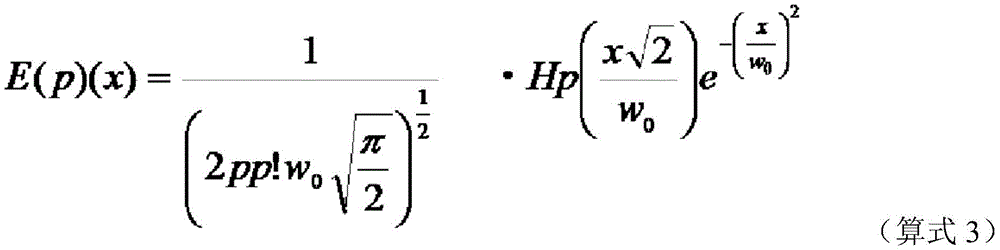
H0(x)=1,H1(x)=2x,H2(x)=4x2-2,H3(x)=8x3-12x (算式4)H 0 (x)=1, H 1 (x)=2x, H 2 (x)=4x 2 -2, H 3 (x)=8x 3 -12x (Equation 4)
也能通过调整各模式光的强度,来使合波后的光束形状变为接近于高斯光束(gaussian)的形状。如图10所示,可以理解的是,与零次模光以及二次模光相比,零次模光和二次模光的合波光具有更高强度并且更小的光斑直径。如此,根据本实施例二的光合波回路,能通过将导波模式不同的RGB的各波长的光合波到在零次模下对RGB的各波长的光进行了合波的波导并射出,来输出更高强度并且光斑直径更小的合波光。By adjusting the intensity of each mode light, the shape of the combined beam can be changed to a shape close to a Gaussian beam. As shown in FIG. 10 , it can be understood that, compared with the zero-order mode light and the second-order mode light, the combined wave light of the zero-order mode light and the second-order mode light has a higher intensity and a smaller spot diameter. In this way, according to the optical multiplexing circuit of the second embodiment, the light of each wavelength of RGB with different guiding modes can be multiplexed into a waveguide that multiplexed the light of each wavelength of RGB in the zero-order mode, and then outputted. Combined light with higher intensity and smaller spot diameter is output.
在本实施例二中,对将零次模光和二次模光合波的例子进行了说明,但是,根据本实施例二,调整有效折射率就能与导波模式无关地进行合波。通过对波长组λ1、λ2、λ3的光分配不同的导波模式,能按照所使用的导波模式的数量对这些波长群的光进行合波。例如,能通过使用零次至三次的导波模式的光来对四个红、绿、蓝的光进行合波并射出。In the second embodiment, the example in which the zero-order mode light and the second-order mode light are combined has been described. However, according to the second embodiment, the multiplexing can be performed regardless of the guided wave mode by adjusting the effective refractive index. By assigning different guided wave modes to the lights of the wavelength groups λ1 , λ2 , and λ3 , the light of these wavelength groups can be multiplexed according to the number of the guided wave modes used. For example, four red, green, and blue lights can be combined and output by using light in the zero-order to third-order guided wave mode.
在本实施例二中,虽然设为λ1=450nm(蓝)、λ2=520nm(绿)、λ3=650nm(红),但并不限定于此,波长λ1、λ2、以及λ3的光能分别设为具有蓝(400~495nm)、绿(495~570nm)、红(620~750nm)的波长区域的波长的光。In the second embodiment, although λ1=450nm (blue), λ2=520nm (green), and λ3=650nm (red), it is not limited to this, and the light energy of wavelengths λ1, λ2, and λ3 are respectively set as It is light having wavelengths in the wavelength regions of blue (400 to 495 nm), green (495 to 570 nm), and red (620 to 750 nm).
(实施例三)(Example 3)
参照图11,对本发明的实施例三的光合波回路进行具体说明。在本实施例三中,示出了一种光合波回路,其具备以下功能:实施例一那样的仅对所希望的波长的光进行耦合并合波的功能;以及实施例二那样的通过对导波模式不同的各波长的光进行合波来输出更高强度的合波光的功能。Referring to FIG. 11 , the optical multiplexing circuit according to the third embodiment of the present invention will be described in detail. In the third embodiment, an optical multiplexing circuit is shown, which has the following functions: as in the first embodiment, only the function of coupling and multiplexing light of a desired wavelength; The function of combining light of each wavelength with different guided wave modes to output the combined light of higher intensity.
在图11中示出了一种光合波回路,其具备:供波长λ1、λ2、λ3、λ2’、以及λ3’的光分别输入的第一至第五光波导301~305;第一和第二MM转换波导306、307;第一至第四耦合部308~311;第一和第二合波部312、313;以及耦合于第一光波导301的输出波导314。FIG. 11 shows an optical multiplexing circuit including: first to fifth
第一至第五光波导301~305和第一和第二MM转换波导306、307由设于基板上的下部包层、比下部包层折射率高的芯层、以及设于芯层上的上部包层构成。上部包层设为包围芯层。第一光波导301能采用多模波导。第二至第五光波导302~305能采用单模波导。如图11所示,第一至第五光波导301~305和第一和第二MM转换波导306、307相对于光的行进方向并列配置。第一光波导301包含波导宽度各不相同的第一和第二部分3011、3012。第一和第二部分3011、3012与输出波导315的每一个之间经由锥形的波导进行耦合。The first to fifth
在本实施例三中,第一至第五光波导301~305与第一和第二MM转换波导306、307的波导宽度不同。第一至第四耦合部308~311分别采用通过使第二光波导302以及第一MM转换波导306、第一光波导301以及第一MM转换波导306、第三光波导303以及第二MM转换波导307、第一光波导301与第二MM转换波导307接近而构成的定向耦合器。第一和第二合波部312、313分别采用通过使第四光波导304以及第一光波导301、第五光波导305以及第一光波导301接近而构成的定向耦合器。In the third embodiment, the waveguide widths of the first to fifth
与实施例一同样,第一和第二光波导301、302的波导宽度和第一MM转换波导306的波导宽度设定为:相对于第二光波导302而言的波长λ2的光的零次模下的有效折射率与相对于第一MM转换波导306而言的波长λ2的光的高次模下的有效折射率相等,并且,相对于第一光波导301而言的波长λ1的光的零次模下的有效折射率与相对于第一MM转换波导306而言的波长λ1的各光的高次模下的有效折射率不相等。此外,第一和第三光波导301、303的波导宽度和第二MM转换波导307的波导宽度设定为:相对于第三光波导303而言的波长λ3的光的零次模下的有效折射率与相对于第二MM转换波导307而言的波长λ3的光的高次模下的有效折射率相等,并且相对于第一光波导301而言的波长λ1的光的零次模下的有效折射率与相对于第二MM转换波导307而言的波长λ1以及λ2的各光的高次模下的有效折射率不相等。As in the first embodiment, the waveguide widths of the first and second
而且,与本实施例二同样,第一部分3011的波导宽度设定为:相对于第四光波导304而言的波长λ2’的光的零次模下的有效折射率与相对于第一光波导301的第一部分3011而言的波长λ2’的光的高次模下的有效折射率相等,并且,相对于第一光波导301的第一部分3011而言的波长λ1、λ2、λ3的光的高次模下的有效折射率与相对于第四光波导304而言的波长λ1、λ2、λ3的光的零次模下的有效折射率不相等。此外,第二部分3012的波导宽度设定为:相对于第五光波导305而言的波长λ3’的光的零次模下的有效折射率与相对于第一光波导301的第二部分3012而言的波长λ3’的光的高次模下的有效折射率相等,并且,相对于第一光波导301的第二部分3012而言的波长λ1、λ2、λ3的光的高次模下的有效折射率与相对于第五光波导305而言的波长λ1、λ2、λ3的光的零次模下的有效折射率不相等。Furthermore, as in the second embodiment, the waveguide width of the
在本实施例三中,波长λ1、λ2以及λ3的光分别设为具有蓝(400~495nm)、绿(495~570nm)、红(620~750nm)的波长区域的波长的光,λ2’=(λ2+β)nm(绿)、λ3’=(λ3+γ)nm(红),β、γ为大于0且小于线宽的微小的值,线宽基于所射入的光的光源但大体上为1nm以下。In the third embodiment, light with wavelengths λ1, λ2, and λ3 is set to light having wavelengths in the wavelength regions of blue (400-495 nm), green (495-570 nm), and red (620-750 nm), respectively, and λ2'= (λ2+β) nm (green), λ3'=(λ3+γ) nm (red), β and γ are small values larger than 0 and smaller than the line width, and the line width is based on the light source of the incident light but generally The upper limit is 1 nm or less.
以下,对本发明的实施例三的光合波回路的动作进行说明。从第二光波导302射入的波长λ2的光在第一耦合部308其导波模式被转换为一次模并转移至第一MM转换波导306,在第二耦合部309其导波模式进一步被转换为零次模并转移至第一光波导301。同样,从第三光波导303射入的波长λ3的光在第三耦合部310其导波模式被转换为一次模并转移至第二MM转换波导307,在第四耦合部311其导波模式进一步被转换为零次模并转移至第一光波导301。Hereinafter, the operation of the optical multiplexing circuit according to the third embodiment of the present invention will be described. The light of wavelength λ2 incident from the second
此外,与上述实施例一同样,以不满足与第一和第二MM转换波导306、307耦合的条件的方式设计了第二和第四耦合部309、311。因此,从第一光波导301射入的零次模的波长λ1的光在第二和第四耦合部309、311不向第一和第二MM转换波导306、307转移而是从第二和第四耦合部309、311透射。其结果是,从第二和第四耦合部309、311透射的波长λ1的光和分别从第二和第三光波导302、303经由第一和第二MM转换波导306、307转移的波长λ2以及λ3的光合波并输入至第一光波导301的第一部分3011。通过以上方式,实施例三的光合波回路能实现实施例一那样的仅对所希望的波长的光进行耦合并合波的功能。Furthermore, as in the first embodiment described above, the second and
另一方面,在第四光波导304传播的零次模的波长λ2’的光在第一合波部312其导波模式被转换为二次模并耦合至第一光波导301的第一部分3011。耦合后的二次模的波长λ2’的光与在第一光波导301的第一部分3011传播的零次模的波长λ1、λ2、λ3的光进行合波,并输入至第一光波导301的第二部分3012。而且,在第五光波导305传播的零次模的波长λ3’的光在第二合波部313其导波模式被转换为二次模并耦合至第一光波导301的第二部分3012。耦合后的二次模的波长λ3’的光与在第一光波导301的第二部分3012传播的合波光进行合波,并从输出波导314输出。通过以上方式,实施例三的光合波回路能实现实施例二那样的通过对导波模式不同的各波长的光进行合波来输出更高强度的合波光的功能。On the other hand, the light of wavelength λ2 ′ of the zeroth-order mode propagating in the fourth
在实施例三的光合波回路中,与实施例一以及二同样,例如,假定λ1=450nm,λ2=520nm,λ3=650nm,波导膜厚为3.6μm,相对折射率差Δ为0.45%,第一至第四耦合部308~311、第四光波导304与第一部分3011以及第五光波导305与第二部分3012的波导间间隙分别为2.5μm,第一至第四耦合部308~311的耦合长度为702μm,第一合波部312的耦合长度为2380μm,第二合波部313的耦合长度为900μm,第一至第五光波导301~305的波导宽度为1.5μm。该情况下,基于图5以及图9,能通过设为:第一MM转换波导306的波导宽度为4.3μm,第二MM转换波导307的波导宽度为4.8μm,第一部分3011的波导宽度为7.15μm,第二部分3012的波导宽度为8.00μm,来实现实施例三的光合波回路。In the optical multiplexing circuit of the third embodiment, as in the first and second embodiments, for example, assuming that λ1 = 450 nm, λ2 = 520 nm, λ3 = 650 nm, the waveguide film thickness is 3.6 μm, and the relative refractive index difference Δ is 0.45%, the first The gaps between the first to fourth coupling parts 308-311, the fourth
在此,在上述实施例中对使用了定向耦合器来作为耦合部的情况进行了说明,但是,例如也可以使用2×1的MMI、其他的合波器,这一点自不必说。此外,在上述实施例中,以RGB耦合模块为例进行了说明,但如果是将多个波长的多个光合波至一条波导的情况,则能不受材料、相对折射率差Δ限制地应用本发明,这一点自不必说。而且,由于本发明的波导形状不依赖于平面波导的材料、相对折射率差Δ,因此对所有波导都能适用。而且,在上述实施例中,举例示出了作为可见光的三原色RGB光合波回路,但本发明能作为对波长不同的多个光进行合波以及分波的光合分波回路来应用,这一点是明确的。Here, in the above-described embodiment, the case where a directional coupler is used as the coupling unit has been described, but it goes without saying that, for example, a 2×1 MMI or other multiplexer may be used. In addition, in the above-mentioned embodiment, the RGB coupling module is used as an example for description, but if it is a case of multiplexing a plurality of wavelengths of light into a single waveguide, it can be applied regardless of the material or the relative refractive index difference Δ The present invention, needless to say. Furthermore, since the waveguide shape of the present invention does not depend on the material of the planar waveguide and the relative refractive index difference Δ, it can be applied to all waveguides. Furthermore, in the above-mentioned embodiments, the three-primary-color RGB optical multiplexing circuit is shown as an example of visible light, but the present invention can be applied as an optical multiplexing and demultiplexing circuit for multiplexing and demultiplexing a plurality of lights with different wavelengths. clearly.
Claims (6)
Priority Applications (1)
| Application Number | Priority Date | Filing Date | Title |
|---|---|---|---|
| CN202010327303.XA CN111487713B (en) | 2016-02-18 | 2017-02-17 | optical multiplexer circuit |
Applications Claiming Priority (5)
| Application Number | Priority Date | Filing Date | Title |
|---|---|---|---|
| JP2016029366 | 2016-02-18 | ||
| JP2016-029366 | 2016-02-18 | ||
| JP2016029361 | 2016-02-18 | ||
| JP2016-029361 | 2016-02-18 | ||
| PCT/JP2017/005975 WO2017142076A1 (en) | 2016-02-18 | 2017-02-17 | Optical multiplexing circuit |
Related Child Applications (1)
| Application Number | Title | Priority Date | Filing Date |
|---|---|---|---|
| CN202010327303.XA Division CN111487713B (en) | 2016-02-18 | 2017-02-17 | optical multiplexer circuit |
Publications (2)
| Publication Number | Publication Date |
|---|---|
| CN108700706A CN108700706A (en) | 2018-10-23 |
| CN108700706B true CN108700706B (en) | 2020-08-04 |
Family
ID=59625276
Family Applications (2)
| Application Number | Title | Priority Date | Filing Date |
|---|---|---|---|
| CN202010327303.XA Active CN111487713B (en) | 2016-02-18 | 2017-02-17 | optical multiplexer circuit |
| CN201780011275.7A Active CN108700706B (en) | 2016-02-18 | 2017-02-17 | Optical multiplexer circuit |
Family Applications Before (1)
| Application Number | Title | Priority Date | Filing Date |
|---|---|---|---|
| CN202010327303.XA Active CN111487713B (en) | 2016-02-18 | 2017-02-17 | optical multiplexer circuit |
Country Status (5)
| Country | Link |
|---|---|
| US (2) | US10649144B2 (en) |
| EP (4) | EP3767352B1 (en) |
| JP (1) | JP6572377B2 (en) |
| CN (2) | CN111487713B (en) |
| WO (1) | WO2017142076A1 (en) |
Families Citing this family (18)
| Publication number | Priority date | Publication date | Assignee | Title |
|---|---|---|---|---|
| EP3767352B1 (en) | 2016-02-18 | 2022-04-20 | Nippon Telegraph and Telephone Corporation | Optical multiplexing circuit |
| CN108254829A (en) * | 2018-01-04 | 2018-07-06 | 华南师范大学 | A kind of design method of the vertical pattern converter of double, asymmetrical |
| JP6994220B2 (en) * | 2018-03-01 | 2022-01-14 | 日本電信電話株式会社 | Wavelength combiner |
| JP7172271B2 (en) * | 2018-08-10 | 2022-11-16 | 日本電信電話株式会社 | Optical multiplexer and RGB coupler |
| JP7189432B2 (en) * | 2019-01-10 | 2022-12-14 | 日本電信電話株式会社 | optical signal processor |
| JP7172642B2 (en) * | 2019-01-23 | 2022-11-16 | 日本電信電話株式会社 | Mode multiplexing/demultiplexing optical circuit |
| JP7120053B2 (en) * | 2019-01-29 | 2022-08-17 | 日本電信電話株式会社 | optical circuit |
| CN112514184A (en) * | 2019-03-13 | 2021-03-16 | 国立大学法人福井大学 | Optical waveguide type optical multiplexer, optical waveguide type optical multiplexer light source device, and image projection device |
| WO2020245923A1 (en) * | 2019-06-04 | 2020-12-10 | 日本電信電話株式会社 | Optical circuit |
| JPWO2021002254A1 (en) * | 2019-07-02 | 2021-01-07 | ||
| JP7287242B2 (en) * | 2019-11-06 | 2023-06-06 | 住友電気工業株式会社 | optical module |
| US11768342B2 (en) * | 2020-05-18 | 2023-09-26 | Nippon Telegraph And Telephone Corporation | Optical multiplexing circuit and optical source |
| US12050342B2 (en) * | 2021-02-05 | 2024-07-30 | University Of Fukui | Optical multiplexer and optical multiplexing method |
| JP2023104721A (en) * | 2022-01-18 | 2023-07-28 | セーレンKst株式会社 | optical multiplexer |
| CN114280729B (en) * | 2022-02-10 | 2024-06-14 | 苏州龙马璞芯芯片科技有限公司 | Optical waveguide type light combiner and projection device using same |
| CN114966969B (en) * | 2022-05-27 | 2024-05-24 | 师大海能应急科技(清远)有限公司 | Parallel multimode cross structure based on asymmetric directional coupler |
| US11968034B2 (en) | 2022-08-18 | 2024-04-23 | X Development Llc | Metastructured photonic devices for binary tree multiplexing or demultiplexing of optical signals |
| JP2024058207A (en) * | 2022-10-14 | 2024-04-25 | Tdk株式会社 | Optical multiplexer and visible radiation light source module |
Citations (9)
| Publication number | Priority date | Publication date | Assignee | Title |
|---|---|---|---|---|
| EP1344095A2 (en) * | 2000-11-14 | 2003-09-17 | Optun (BVI) Ltd. | Optical mode coupling devices and an optical switch matrix based thereon |
| JP2004093884A (en) * | 2002-08-30 | 2004-03-25 | Kyocera Corp | Multiplexing / demultiplexing device for different wavelength multiplexed light, optical amplifier and ASE light source using the same |
| JP2006323319A (en) * | 2005-05-20 | 2006-11-30 | Sumitomo Bakelite Co Ltd | Optical waveguide structure |
| CN101504472A (en) * | 2008-02-08 | 2009-08-12 | 冲电气工业株式会社 | Optical multiplexing/demultiplexing device |
| WO2010137661A1 (en) * | 2009-05-28 | 2010-12-02 | シチズンホールディングス株式会社 | Light source device |
| JP2013174752A (en) * | 2012-02-27 | 2013-09-05 | Oki Electric Ind Co Ltd | Wavelength selective path switching element |
| JP2014119556A (en) * | 2012-12-14 | 2014-06-30 | Nippon Telegr & Teleph Corp <Ntt> | Mode multiplexer/demultiplexer |
| CN104749707A (en) * | 2015-01-28 | 2015-07-01 | 浙江大学 | Weak-confined large-cross-section optical waveguide based dual-polarization mode multiplexing-demultiplexing device |
| CN104849803A (en) * | 2014-02-17 | 2015-08-19 | 株式会社藤仓 | Substrate-type waveguide element and optical modulator |
Family Cites Families (13)
| Publication number | Priority date | Publication date | Assignee | Title |
|---|---|---|---|---|
| JP4652507B2 (en) * | 1998-12-25 | 2011-03-16 | 古河電気工業株式会社 | Optical waveguide circuit and manufacturing method thereof |
| US6603592B1 (en) * | 2000-09-26 | 2003-08-05 | Lucent Technologies Inc. | Optical wavelength converter |
| US20040096141A1 (en) * | 2002-11-18 | 2004-05-20 | Harmeet Singh | Optical multiplexer |
| US7961997B2 (en) | 2003-09-22 | 2011-06-14 | Celight, Inc. | Space diversity optical receiver and system and method using the same |
| WO2008108422A1 (en) * | 2007-03-07 | 2008-09-12 | Nec Corporation | Optical waveguide module |
| US7539373B1 (en) * | 2007-11-26 | 2009-05-26 | Onechip Photonics Inc. | Integrated lateral mode converter |
| WO2010084796A1 (en) * | 2009-01-23 | 2010-07-29 | 株式会社フジクラ | Optical multiplexer and fiber laser |
| US8965156B2 (en) * | 2010-08-12 | 2015-02-24 | Octrolix Bv | Beam combiner |
| US9306670B2 (en) * | 2011-09-27 | 2016-04-05 | Nippon Telegraph And Telephone Corporation | Optical coupling/splitting device, two-way optical propagation device, and optical-transmit-receive system |
| JP5822789B2 (en) * | 2012-05-23 | 2015-11-24 | 三菱電機株式会社 | Optical multiplexer / demultiplexer |
| JP6000904B2 (en) * | 2013-06-27 | 2016-10-05 | 株式会社フジクラ | Polarization conversion element |
| US10408999B2 (en) * | 2014-05-09 | 2019-09-10 | National University Corporation University Of Fukui | Multiplexer |
| EP3767352B1 (en) * | 2016-02-18 | 2022-04-20 | Nippon Telegraph and Telephone Corporation | Optical multiplexing circuit |
-
2017
- 2017-02-17 EP EP20175143.5A patent/EP3767352B1/en active Active
- 2017-02-17 CN CN202010327303.XA patent/CN111487713B/en active Active
- 2017-02-17 EP EP20209717.6A patent/EP3800491A1/en not_active Withdrawn
- 2017-02-17 WO PCT/JP2017/005975 patent/WO2017142076A1/en not_active Ceased
- 2017-02-17 CN CN201780011275.7A patent/CN108700706B/en active Active
- 2017-02-17 JP JP2018500229A patent/JP6572377B2/en active Active
- 2017-02-17 US US16/077,940 patent/US10649144B2/en active Active
- 2017-02-17 EP EP17753330.4A patent/EP3418783A4/en not_active Ceased
- 2017-02-17 EP EP21177930.1A patent/EP3896505B1/en active Active
-
2020
- 2020-04-10 US US16/845,523 patent/US11112563B2/en active Active
Patent Citations (9)
| Publication number | Priority date | Publication date | Assignee | Title |
|---|---|---|---|---|
| EP1344095A2 (en) * | 2000-11-14 | 2003-09-17 | Optun (BVI) Ltd. | Optical mode coupling devices and an optical switch matrix based thereon |
| JP2004093884A (en) * | 2002-08-30 | 2004-03-25 | Kyocera Corp | Multiplexing / demultiplexing device for different wavelength multiplexed light, optical amplifier and ASE light source using the same |
| JP2006323319A (en) * | 2005-05-20 | 2006-11-30 | Sumitomo Bakelite Co Ltd | Optical waveguide structure |
| CN101504472A (en) * | 2008-02-08 | 2009-08-12 | 冲电气工业株式会社 | Optical multiplexing/demultiplexing device |
| WO2010137661A1 (en) * | 2009-05-28 | 2010-12-02 | シチズンホールディングス株式会社 | Light source device |
| JP2013174752A (en) * | 2012-02-27 | 2013-09-05 | Oki Electric Ind Co Ltd | Wavelength selective path switching element |
| JP2014119556A (en) * | 2012-12-14 | 2014-06-30 | Nippon Telegr & Teleph Corp <Ntt> | Mode multiplexer/demultiplexer |
| CN104849803A (en) * | 2014-02-17 | 2015-08-19 | 株式会社藤仓 | Substrate-type waveguide element and optical modulator |
| CN104749707A (en) * | 2015-01-28 | 2015-07-01 | 浙江大学 | Weak-confined large-cross-section optical waveguide based dual-polarization mode multiplexing-demultiplexing device |
Also Published As
| Publication number | Publication date |
|---|---|
| EP3418783A1 (en) | 2018-12-26 |
| EP3418783A4 (en) | 2019-11-20 |
| US20190056552A1 (en) | 2019-02-21 |
| EP3896505A1 (en) | 2021-10-20 |
| CN108700706A (en) | 2018-10-23 |
| EP3767352B1 (en) | 2022-04-20 |
| US11112563B2 (en) | 2021-09-07 |
| EP3896505B1 (en) | 2023-10-11 |
| CN111487713A (en) | 2020-08-04 |
| WO2017142076A1 (en) | 2017-08-24 |
| US20200241206A1 (en) | 2020-07-30 |
| EP3800491A1 (en) | 2021-04-07 |
| CN111487713B (en) | 2023-01-24 |
| US10649144B2 (en) | 2020-05-12 |
| JPWO2017142076A1 (en) | 2018-08-09 |
| JP6572377B2 (en) | 2019-09-11 |
| EP3767352A1 (en) | 2021-01-20 |
Similar Documents
| Publication | Publication Date | Title |
|---|---|---|
| CN108700706B (en) | Optical multiplexer circuit | |
| JP6276840B2 (en) | Polarization rotation circuit | |
| JP6691518B2 (en) | Optical integrated circuit | |
| CN107450126A (en) | A kind of polarization beam apparatus and its design method | |
| JP4477260B2 (en) | Waveguide-type optical coupler and optical multiplexer / demultiplexer using the waveguide-type optical coupler | |
| JP6697423B2 (en) | Optical integrated circuit | |
| WO2014030576A1 (en) | Optical waveguide element | |
| US11543591B2 (en) | Optical multiplexer and RGB coupler | |
| JPWO2020213067A1 (en) | Photosynthetic circuit and light source | |
| Truong et al. | A design of triplexer based on a 2× 2 butterfly MMI coupler and a directional coupler using silicon waveguides | |
| JP7295458B2 (en) | optical circuit | |
| JP7295459B2 (en) | optical multiplexing circuit | |
| JP7097332B2 (en) | Combined demultiplexing element and light source module | |
| JP2019117236A (en) | Optical circuit capable of suppressing loss due to light radiated from bend waveguide and light source with monitoring function using said optical circuit | |
| JP2017134222A (en) | Optical waveguide device | |
| WO2021002254A1 (en) | Optical multiplexer | |
| JP6539195B2 (en) | Light circuit | |
| Malka | 1x4 Visible Light MMI Wavelength Demultiplexer in GaN slot-Waveguide Structure | |
| JP7120053B2 (en) | optical circuit | |
| WO2025013201A1 (en) | Mode filter and optical circuit provided with same | |
| JP2018194665A (en) | Wavelength separation element | |
| Trung et al. | Numerical Design of a Waveguide Crossing Based on SOI platform for Wideband Photonic Integrated Circuits and Networks | |
| KR20240134022A (en) | Optical splitter | |
| WO2024171357A1 (en) | Optical circuit | |
| WO2019160031A1 (en) | Ring resonator filter and method for designing same |
Legal Events
| Date | Code | Title | Description |
|---|---|---|---|
| PB01 | Publication | ||
| PB01 | Publication | ||
| SE01 | Entry into force of request for substantive examination | ||
| SE01 | Entry into force of request for substantive examination | ||
| GR01 | Patent grant | ||
| GR01 | Patent grant | ||
| CP03 | Change of name, title or address | ||
| CP03 | Change of name, title or address |
Address after: Tokyo, Japan Patentee after: Entiti Corp. Country or region after: Japan Address before: Tokyo, Japan Patentee before: NIPPON TELEGRAPH AND TELEPHONE Corp. Country or region before: Japan |