JP5973556B2 - 表示装置 - Google Patents
表示装置 Download PDFInfo
- Publication number
- JP5973556B2 JP5973556B2 JP2014511123A JP2014511123A JP5973556B2 JP 5973556 B2 JP5973556 B2 JP 5973556B2 JP 2014511123 A JP2014511123 A JP 2014511123A JP 2014511123 A JP2014511123 A JP 2014511123A JP 5973556 B2 JP5973556 B2 JP 5973556B2
- Authority
- JP
- Japan
- Prior art keywords
- electrode
- transistor
- substrate
- pixel
- gate
- Prior art date
- Legal status (The legal status is an assumption and is not a legal conclusion. Google has not performed a legal analysis and makes no representation as to the accuracy of the status listed.)
- Active
Links
Images




Classifications
-
- H—ELECTRICITY
- H10—SEMICONDUCTOR DEVICES; ELECTRIC SOLID-STATE DEVICES NOT OTHERWISE PROVIDED FOR
- H10K—ORGANIC ELECTRIC SOLID-STATE DEVICES
- H10K59/00—Integrated devices, or assemblies of multiple devices, comprising at least one organic light-emitting element covered by group H10K50/00
- H10K59/80—Constructional details
- H10K59/87—Passivation; Containers; Encapsulations
-
- G—PHYSICS
- G02—OPTICS
- G02F—OPTICAL DEVICES OR ARRANGEMENTS FOR THE CONTROL OF LIGHT BY MODIFICATION OF THE OPTICAL PROPERTIES OF THE MEDIA OF THE ELEMENTS INVOLVED THEREIN; NON-LINEAR OPTICS; FREQUENCY-CHANGING OF LIGHT; OPTICAL LOGIC ELEMENTS; OPTICAL ANALOGUE/DIGITAL CONVERTERS
- G02F1/00—Devices or arrangements for the control of the intensity, colour, phase, polarisation or direction of light arriving from an independent light source, e.g. switching, gating or modulating; Non-linear optics
- G02F1/01—Devices or arrangements for the control of the intensity, colour, phase, polarisation or direction of light arriving from an independent light source, e.g. switching, gating or modulating; Non-linear optics for the control of the intensity, phase, polarisation or colour
- G02F1/13—Devices or arrangements for the control of the intensity, colour, phase, polarisation or direction of light arriving from an independent light source, e.g. switching, gating or modulating; Non-linear optics for the control of the intensity, phase, polarisation or colour based on liquid crystals, e.g. single liquid crystal display cells
- G02F1/133—Constructional arrangements; Operation of liquid crystal cells; Circuit arrangements
- G02F1/1333—Constructional arrangements; Manufacturing methods
- G02F1/1339—Gaskets; Spacers; Sealing of cells
-
- G—PHYSICS
- G02—OPTICS
- G02F—OPTICAL DEVICES OR ARRANGEMENTS FOR THE CONTROL OF LIGHT BY MODIFICATION OF THE OPTICAL PROPERTIES OF THE MEDIA OF THE ELEMENTS INVOLVED THEREIN; NON-LINEAR OPTICS; FREQUENCY-CHANGING OF LIGHT; OPTICAL LOGIC ELEMENTS; OPTICAL ANALOGUE/DIGITAL CONVERTERS
- G02F1/00—Devices or arrangements for the control of the intensity, colour, phase, polarisation or direction of light arriving from an independent light source, e.g. switching, gating or modulating; Non-linear optics
- G02F1/01—Devices or arrangements for the control of the intensity, colour, phase, polarisation or direction of light arriving from an independent light source, e.g. switching, gating or modulating; Non-linear optics for the control of the intensity, phase, polarisation or colour
- G02F1/13—Devices or arrangements for the control of the intensity, colour, phase, polarisation or direction of light arriving from an independent light source, e.g. switching, gating or modulating; Non-linear optics for the control of the intensity, phase, polarisation or colour based on liquid crystals, e.g. single liquid crystal display cells
- G02F1/133—Constructional arrangements; Operation of liquid crystal cells; Circuit arrangements
- G02F1/13306—Circuit arrangements or driving methods for the control of single liquid crystal cells
-
- G—PHYSICS
- G02—OPTICS
- G02F—OPTICAL DEVICES OR ARRANGEMENTS FOR THE CONTROL OF LIGHT BY MODIFICATION OF THE OPTICAL PROPERTIES OF THE MEDIA OF THE ELEMENTS INVOLVED THEREIN; NON-LINEAR OPTICS; FREQUENCY-CHANGING OF LIGHT; OPTICAL LOGIC ELEMENTS; OPTICAL ANALOGUE/DIGITAL CONVERTERS
- G02F1/00—Devices or arrangements for the control of the intensity, colour, phase, polarisation or direction of light arriving from an independent light source, e.g. switching, gating or modulating; Non-linear optics
- G02F1/01—Devices or arrangements for the control of the intensity, colour, phase, polarisation or direction of light arriving from an independent light source, e.g. switching, gating or modulating; Non-linear optics for the control of the intensity, phase, polarisation or colour
- G02F1/13—Devices or arrangements for the control of the intensity, colour, phase, polarisation or direction of light arriving from an independent light source, e.g. switching, gating or modulating; Non-linear optics for the control of the intensity, phase, polarisation or colour based on liquid crystals, e.g. single liquid crystal display cells
- G02F1/133—Constructional arrangements; Operation of liquid crystal cells; Circuit arrangements
- G02F1/1333—Constructional arrangements; Manufacturing methods
- G02F1/1341—Filling or closing of cells
-
- G—PHYSICS
- G02—OPTICS
- G02F—OPTICAL DEVICES OR ARRANGEMENTS FOR THE CONTROL OF LIGHT BY MODIFICATION OF THE OPTICAL PROPERTIES OF THE MEDIA OF THE ELEMENTS INVOLVED THEREIN; NON-LINEAR OPTICS; FREQUENCY-CHANGING OF LIGHT; OPTICAL LOGIC ELEMENTS; OPTICAL ANALOGUE/DIGITAL CONVERTERS
- G02F1/00—Devices or arrangements for the control of the intensity, colour, phase, polarisation or direction of light arriving from an independent light source, e.g. switching, gating or modulating; Non-linear optics
- G02F1/01—Devices or arrangements for the control of the intensity, colour, phase, polarisation or direction of light arriving from an independent light source, e.g. switching, gating or modulating; Non-linear optics for the control of the intensity, phase, polarisation or colour
- G02F1/13—Devices or arrangements for the control of the intensity, colour, phase, polarisation or direction of light arriving from an independent light source, e.g. switching, gating or modulating; Non-linear optics for the control of the intensity, phase, polarisation or colour based on liquid crystals, e.g. single liquid crystal display cells
- G02F1/133—Constructional arrangements; Operation of liquid crystal cells; Circuit arrangements
- G02F1/1333—Constructional arrangements; Manufacturing methods
- G02F1/1345—Conductors connecting electrodes to cell terminals
- G02F1/13452—Conductors connecting driver circuitry and terminals of panels
-
- G—PHYSICS
- G02—OPTICS
- G02F—OPTICAL DEVICES OR ARRANGEMENTS FOR THE CONTROL OF LIGHT BY MODIFICATION OF THE OPTICAL PROPERTIES OF THE MEDIA OF THE ELEMENTS INVOLVED THEREIN; NON-LINEAR OPTICS; FREQUENCY-CHANGING OF LIGHT; OPTICAL LOGIC ELEMENTS; OPTICAL ANALOGUE/DIGITAL CONVERTERS
- G02F1/00—Devices or arrangements for the control of the intensity, colour, phase, polarisation or direction of light arriving from an independent light source, e.g. switching, gating or modulating; Non-linear optics
- G02F1/01—Devices or arrangements for the control of the intensity, colour, phase, polarisation or direction of light arriving from an independent light source, e.g. switching, gating or modulating; Non-linear optics for the control of the intensity, phase, polarisation or colour
- G02F1/13—Devices or arrangements for the control of the intensity, colour, phase, polarisation or direction of light arriving from an independent light source, e.g. switching, gating or modulating; Non-linear optics for the control of the intensity, phase, polarisation or colour based on liquid crystals, e.g. single liquid crystal display cells
- G02F1/133—Constructional arrangements; Operation of liquid crystal cells; Circuit arrangements
- G02F1/1333—Constructional arrangements; Manufacturing methods
- G02F1/1345—Conductors connecting electrodes to cell terminals
- G02F1/13454—Drivers integrated on the active matrix substrate
-
- G—PHYSICS
- G02—OPTICS
- G02F—OPTICAL DEVICES OR ARRANGEMENTS FOR THE CONTROL OF LIGHT BY MODIFICATION OF THE OPTICAL PROPERTIES OF THE MEDIA OF THE ELEMENTS INVOLVED THEREIN; NON-LINEAR OPTICS; FREQUENCY-CHANGING OF LIGHT; OPTICAL LOGIC ELEMENTS; OPTICAL ANALOGUE/DIGITAL CONVERTERS
- G02F1/00—Devices or arrangements for the control of the intensity, colour, phase, polarisation or direction of light arriving from an independent light source, e.g. switching, gating or modulating; Non-linear optics
- G02F1/01—Devices or arrangements for the control of the intensity, colour, phase, polarisation or direction of light arriving from an independent light source, e.g. switching, gating or modulating; Non-linear optics for the control of the intensity, phase, polarisation or colour
- G02F1/13—Devices or arrangements for the control of the intensity, colour, phase, polarisation or direction of light arriving from an independent light source, e.g. switching, gating or modulating; Non-linear optics for the control of the intensity, phase, polarisation or colour based on liquid crystals, e.g. single liquid crystal display cells
- G02F1/133—Constructional arrangements; Operation of liquid crystal cells; Circuit arrangements
- G02F1/136—Liquid crystal cells structurally associated with a semi-conducting layer or substrate, e.g. cells forming part of an integrated circuit
- G02F1/1362—Active matrix addressed cells
- G02F1/136286—Wiring, e.g. gate line, drain line
-
- G—PHYSICS
- G02—OPTICS
- G02F—OPTICAL DEVICES OR ARRANGEMENTS FOR THE CONTROL OF LIGHT BY MODIFICATION OF THE OPTICAL PROPERTIES OF THE MEDIA OF THE ELEMENTS INVOLVED THEREIN; NON-LINEAR OPTICS; FREQUENCY-CHANGING OF LIGHT; OPTICAL LOGIC ELEMENTS; OPTICAL ANALOGUE/DIGITAL CONVERTERS
- G02F1/00—Devices or arrangements for the control of the intensity, colour, phase, polarisation or direction of light arriving from an independent light source, e.g. switching, gating or modulating; Non-linear optics
- G02F1/01—Devices or arrangements for the control of the intensity, colour, phase, polarisation or direction of light arriving from an independent light source, e.g. switching, gating or modulating; Non-linear optics for the control of the intensity, phase, polarisation or colour
- G02F1/13—Devices or arrangements for the control of the intensity, colour, phase, polarisation or direction of light arriving from an independent light source, e.g. switching, gating or modulating; Non-linear optics for the control of the intensity, phase, polarisation or colour based on liquid crystals, e.g. single liquid crystal display cells
- G02F1/133—Constructional arrangements; Operation of liquid crystal cells; Circuit arrangements
- G02F1/136—Liquid crystal cells structurally associated with a semi-conducting layer or substrate, e.g. cells forming part of an integrated circuit
- G02F1/1362—Active matrix addressed cells
- G02F1/1368—Active matrix addressed cells in which the switching element is a three-electrode device
-
- G—PHYSICS
- G09—EDUCATION; CRYPTOGRAPHY; DISPLAY; ADVERTISING; SEALS
- G09G—ARRANGEMENTS OR CIRCUITS FOR CONTROL OF INDICATING DEVICES USING STATIC MEANS TO PRESENT VARIABLE INFORMATION
- G09G3/00—Control arrangements or circuits, of interest only in connection with visual indicators other than cathode-ray tubes
- G09G3/20—Control arrangements or circuits, of interest only in connection with visual indicators other than cathode-ray tubes for presentation of an assembly of a number of characters, e.g. a page, by composing the assembly by combination of individual elements arranged in a matrix no fixed position being assigned to or needed to be assigned to the individual characters or partial characters
- G09G3/34—Control arrangements or circuits, of interest only in connection with visual indicators other than cathode-ray tubes for presentation of an assembly of a number of characters, e.g. a page, by composing the assembly by combination of individual elements arranged in a matrix no fixed position being assigned to or needed to be assigned to the individual characters or partial characters by control of light from an independent source
- G09G3/36—Control arrangements or circuits, of interest only in connection with visual indicators other than cathode-ray tubes for presentation of an assembly of a number of characters, e.g. a page, by composing the assembly by combination of individual elements arranged in a matrix no fixed position being assigned to or needed to be assigned to the individual characters or partial characters by control of light from an independent source using liquid crystals
- G09G3/3611—Control of matrices with row and column drivers
- G09G3/3648—Control of matrices with row and column drivers using an active matrix
-
- G—PHYSICS
- G09—EDUCATION; CRYPTOGRAPHY; DISPLAY; ADVERTISING; SEALS
- G09G—ARRANGEMENTS OR CIRCUITS FOR CONTROL OF INDICATING DEVICES USING STATIC MEANS TO PRESENT VARIABLE INFORMATION
- G09G3/00—Control arrangements or circuits, of interest only in connection with visual indicators other than cathode-ray tubes
- G09G3/20—Control arrangements or circuits, of interest only in connection with visual indicators other than cathode-ray tubes for presentation of an assembly of a number of characters, e.g. a page, by composing the assembly by combination of individual elements arranged in a matrix no fixed position being assigned to or needed to be assigned to the individual characters or partial characters
- G09G3/34—Control arrangements or circuits, of interest only in connection with visual indicators other than cathode-ray tubes for presentation of an assembly of a number of characters, e.g. a page, by composing the assembly by combination of individual elements arranged in a matrix no fixed position being assigned to or needed to be assigned to the individual characters or partial characters by control of light from an independent source
- G09G3/36—Control arrangements or circuits, of interest only in connection with visual indicators other than cathode-ray tubes for presentation of an assembly of a number of characters, e.g. a page, by composing the assembly by combination of individual elements arranged in a matrix no fixed position being assigned to or needed to be assigned to the individual characters or partial characters by control of light from an independent source using liquid crystals
- G09G3/3611—Control of matrices with row and column drivers
- G09G3/3674—Details of drivers for scan electrodes
- G09G3/3677—Details of drivers for scan electrodes suitable for active matrices only
-
- H—ELECTRICITY
- H10—SEMICONDUCTOR DEVICES; ELECTRIC SOLID-STATE DEVICES NOT OTHERWISE PROVIDED FOR
- H10D—INORGANIC ELECTRIC SEMICONDUCTOR DEVICES
- H10D30/00—Field-effect transistors [FET]
- H10D30/60—Insulated-gate field-effect transistors [IGFET]
- H10D30/67—Thin-film transistors [TFT]
- H10D30/674—Thin-film transistors [TFT] characterised by the active materials
- H10D30/6755—Oxide semiconductors, e.g. zinc oxide, copper aluminium oxide or cadmium stannate
-
- H—ELECTRICITY
- H10—SEMICONDUCTOR DEVICES; ELECTRIC SOLID-STATE DEVICES NOT OTHERWISE PROVIDED FOR
- H10K—ORGANIC ELECTRIC SOLID-STATE DEVICES
- H10K50/00—Organic light-emitting devices
- H10K50/80—Constructional details
- H10K50/84—Passivation; Containers; Encapsulations
- H10K50/841—Self-supporting sealing arrangements
-
- H—ELECTRICITY
- H10—SEMICONDUCTOR DEVICES; ELECTRIC SOLID-STATE DEVICES NOT OTHERWISE PROVIDED FOR
- H10K—ORGANIC ELECTRIC SOLID-STATE DEVICES
- H10K59/00—Integrated devices, or assemblies of multiple devices, comprising at least one organic light-emitting element covered by group H10K50/00
- H10K59/10—OLED displays
- H10K59/12—Active-matrix OLED [AMOLED] displays
- H10K59/121—Active-matrix OLED [AMOLED] displays characterised by the geometry or disposition of pixel elements
- H10K59/1213—Active-matrix OLED [AMOLED] displays characterised by the geometry or disposition of pixel elements the pixel elements being TFTs
-
- H—ELECTRICITY
- H10—SEMICONDUCTOR DEVICES; ELECTRIC SOLID-STATE DEVICES NOT OTHERWISE PROVIDED FOR
- H10K—ORGANIC ELECTRIC SOLID-STATE DEVICES
- H10K59/00—Integrated devices, or assemblies of multiple devices, comprising at least one organic light-emitting element covered by group H10K50/00
- H10K59/10—OLED displays
- H10K59/12—Active-matrix OLED [AMOLED] displays
- H10K59/123—Connection of the pixel electrodes to the thin film transistors [TFT]
-
- H—ELECTRICITY
- H10—SEMICONDUCTOR DEVICES; ELECTRIC SOLID-STATE DEVICES NOT OTHERWISE PROVIDED FOR
- H10K—ORGANIC ELECTRIC SOLID-STATE DEVICES
- H10K59/00—Integrated devices, or assemblies of multiple devices, comprising at least one organic light-emitting element covered by group H10K50/00
- H10K59/10—OLED displays
- H10K59/12—Active-matrix OLED [AMOLED] displays
- H10K59/131—Interconnections, e.g. wiring lines or terminals
-
- H—ELECTRICITY
- H10—SEMICONDUCTOR DEVICES; ELECTRIC SOLID-STATE DEVICES NOT OTHERWISE PROVIDED FOR
- H10K—ORGANIC ELECTRIC SOLID-STATE DEVICES
- H10K59/00—Integrated devices, or assemblies of multiple devices, comprising at least one organic light-emitting element covered by group H10K50/00
- H10K59/80—Constructional details
- H10K59/805—Electrodes
- H10K59/8051—Anodes
-
- H—ELECTRICITY
- H10—SEMICONDUCTOR DEVICES; ELECTRIC SOLID-STATE DEVICES NOT OTHERWISE PROVIDED FOR
- H10K—ORGANIC ELECTRIC SOLID-STATE DEVICES
- H10K59/00—Integrated devices, or assemblies of multiple devices, comprising at least one organic light-emitting element covered by group H10K50/00
- H10K59/80—Constructional details
- H10K59/87—Passivation; Containers; Encapsulations
- H10K59/871—Self-supporting sealing arrangements
-
- H—ELECTRICITY
- H10—SEMICONDUCTOR DEVICES; ELECTRIC SOLID-STATE DEVICES NOT OTHERWISE PROVIDED FOR
- H10K—ORGANIC ELECTRIC SOLID-STATE DEVICES
- H10K77/00—Constructional details of devices covered by this subclass and not covered by groups H10K10/80, H10K30/80, H10K50/80 or H10K59/80
- H10K77/10—Substrates, e.g. flexible substrates
-
- C—CHEMISTRY; METALLURGY
- C09—DYES; PAINTS; POLISHES; NATURAL RESINS; ADHESIVES; COMPOSITIONS NOT OTHERWISE PROVIDED FOR; APPLICATIONS OF MATERIALS NOT OTHERWISE PROVIDED FOR
- C09J—ADHESIVES; NON-MECHANICAL ASPECTS OF ADHESIVE PROCESSES IN GENERAL; ADHESIVE PROCESSES NOT PROVIDED FOR ELSEWHERE; USE OF MATERIALS AS ADHESIVES
- C09J2301/00—Additional features of adhesives in the form of films or foils
- C09J2301/30—Additional features of adhesives in the form of films or foils characterized by the chemical, physicochemical or physical properties of the adhesive or the carrier
- C09J2301/312—Additional features of adhesives in the form of films or foils characterized by the chemical, physicochemical or physical properties of the adhesive or the carrier parameters being the characterizing feature
-
- G—PHYSICS
- G02—OPTICS
- G02F—OPTICAL DEVICES OR ARRANGEMENTS FOR THE CONTROL OF LIGHT BY MODIFICATION OF THE OPTICAL PROPERTIES OF THE MEDIA OF THE ELEMENTS INVOLVED THEREIN; NON-LINEAR OPTICS; FREQUENCY-CHANGING OF LIGHT; OPTICAL LOGIC ELEMENTS; OPTICAL ANALOGUE/DIGITAL CONVERTERS
- G02F1/00—Devices or arrangements for the control of the intensity, colour, phase, polarisation or direction of light arriving from an independent light source, e.g. switching, gating or modulating; Non-linear optics
- G02F1/01—Devices or arrangements for the control of the intensity, colour, phase, polarisation or direction of light arriving from an independent light source, e.g. switching, gating or modulating; Non-linear optics for the control of the intensity, phase, polarisation or colour
- G02F1/13—Devices or arrangements for the control of the intensity, colour, phase, polarisation or direction of light arriving from an independent light source, e.g. switching, gating or modulating; Non-linear optics for the control of the intensity, phase, polarisation or colour based on liquid crystals, e.g. single liquid crystal display cells
- G02F1/1306—Details
- G02F1/1309—Repairing; Testing
-
- G—PHYSICS
- G09—EDUCATION; CRYPTOGRAPHY; DISPLAY; ADVERTISING; SEALS
- G09G—ARRANGEMENTS OR CIRCUITS FOR CONTROL OF INDICATING DEVICES USING STATIC MEANS TO PRESENT VARIABLE INFORMATION
- G09G2300/00—Aspects of the constitution of display devices
- G09G2300/04—Structural and physical details of display devices
- G09G2300/0404—Matrix technologies
- G09G2300/0408—Integration of the drivers onto the display substrate
-
- G—PHYSICS
- G09—EDUCATION; CRYPTOGRAPHY; DISPLAY; ADVERTISING; SEALS
- G09G—ARRANGEMENTS OR CIRCUITS FOR CONTROL OF INDICATING DEVICES USING STATIC MEANS TO PRESENT VARIABLE INFORMATION
- G09G2300/00—Aspects of the constitution of display devices
- G09G2300/04—Structural and physical details of display devices
- G09G2300/0421—Structural details of the set of electrodes
- G09G2300/0426—Layout of electrodes and connections
-
- G—PHYSICS
- G09—EDUCATION; CRYPTOGRAPHY; DISPLAY; ADVERTISING; SEALS
- G09G—ARRANGEMENTS OR CIRCUITS FOR CONTROL OF INDICATING DEVICES USING STATIC MEANS TO PRESENT VARIABLE INFORMATION
- G09G2300/00—Aspects of the constitution of display devices
- G09G2300/08—Active matrix structure, i.e. with use of active elements, inclusive of non-linear two terminal elements, in the pixels together with light emitting or modulating elements
Landscapes
- Physics & Mathematics (AREA)
- Nonlinear Science (AREA)
- Chemical & Material Sciences (AREA)
- Crystallography & Structural Chemistry (AREA)
- General Physics & Mathematics (AREA)
- Optics & Photonics (AREA)
- Engineering & Computer Science (AREA)
- Mathematical Physics (AREA)
- Microelectronics & Electronic Packaging (AREA)
- Theoretical Computer Science (AREA)
- Computer Hardware Design (AREA)
- Liquid Crystal (AREA)
- Geometry (AREA)
- Devices For Indicating Variable Information By Combining Individual Elements (AREA)
- Control Of Indicators Other Than Cathode Ray Tubes (AREA)
- Liquid Crystal Display Device Control (AREA)
- Electroluminescent Light Sources (AREA)
- Control Of El Displays (AREA)
- Semiconductor Integrated Circuits (AREA)
- Electrochromic Elements, Electrophoresis, Or Variable Reflection Or Absorption Elements (AREA)
Description
本発明に係る表示装置における好ましい実施形態について以下に説明する。なお、以下の好ましい実施形態は、適宜、互いに組み合わされてもよく、以下の2以上の好ましい実施形態を互いに組み合わせた実施形態もまた、好ましい実施形態の一つである。
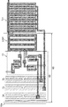
図1〜13を参照して、実施形態1の液晶ディスプレイについて説明する。まず、図1〜3を参照して、本実施形態の液晶ディスプレイの全体の構造について説明する。図1は、実施形態1の液晶ディスプレイに含まれる液晶パネルの平面模式図である。図2は、図1のA−B線における断面模式図である。図3は、実施形態1の液晶ディスプレイに含まれる液晶パネルの平面模式図である。
まず、入力端子INaに入力される信号(スタートパルスSP1、SP2、又は、前々段(各シフトレジスタ内で考えると一段前)の単位回路の出力信号。以下、入力信号INaとも言う。)がローレベルからハイレベルに変化すると、ダイオード接続されたトランジスタTr2を介してノードnetAの電位もハイレベルに変化し、出力トランジスタTr1はオン状態になる。
本実施形態の液晶ディスプレイは、一般的な方法により製造することができるが、より詳細には、まず、アレイ基板10と対向基板50とを通常の方法により各々作製する。
まず、スクリーン印刷法、ディスペンサ描画法等の方法により、アレイ基板10及び対向基板50のいずれかに硬化前のシールの材料(本明細書ではシール材とも言う。)を塗布する。シール材は、閉じた環状に塗布される。また、シール材が塗布された基板、又は、塗布されてない基板上に液晶材料を滴下する。
まず、スクリーン印刷法、ディスペンサ描画法等の方法により、アレイ基板10及び対向基板50のいずれかにシール材を塗布する。シール材は、液晶注入口が形成される領域を除いて、環状に塗布される。
実施形態2の液晶ディスプレイは、ブートストラップ・コンデンサの構造が異なることを除いて、実施形態1の液晶ディスプレイと実質的に同じである。図14は、実施形態2の液晶ディスプレイにおけるブートストラップ・コンデンサの平面模式図である。図15は、図14のJ−K線における断面模式図である。
実施形態3の液晶ディスプレイは、シフトレジスタ中の素子のレイアウトが異なることを除いて、実施形態1の液晶ディスプレイと実質的に同じである。図16は、実施形態3の液晶ディスプレイの額縁領域における構成を示す平面模式図である。
実施形態4の液晶ディスプレイは、シフトレジスタ中の素子のレイアウトが異なることを除いて、実施形態1の液晶ディスプレイと実質的に同じである。図22は、実施形態4の液晶ディスプレイの額縁領域における構成を示す平面模式図である。図23は、図22のM−N線における断面模式図である。
実施形態5の液晶ディスプレイは、コンデンサ部分CAP(2)の平面構造が異なることを除いて、実施形態4の液晶ディスプレイと実質的に同じである。図24は、実施形態5の液晶ディスプレイの額縁領域における構成を示す平面模式図である。
実施形態6の液晶ディスプレイは、シフトレジスタ中の素子のレイアウトが異なることを除いて、実施形態1の液晶ディスプレイと実質的に同じである。図25は、実施形態6の液晶ディスプレイの額縁領域における構成を示す平面模式図である。図26は、図25のP−Q線における断面模式図である。
実施形態7の液晶ディスプレイは、シフトレジスタ中の素子のレイアウトが異なることを除いて、実施形態6の液晶ディスプレイと実質的に同じである。図27は、実施形態7の液晶ディスプレイの額縁領域における構成を示す平面模式図である。
以下にアクティブマトリクス型有機ELディスプレイに係る実施形態8を示す。
図20は、実施形態8のアクティブマトリクス型有機ELディスプレイに含まれる単位画素(画素又はサブ画素)の回路構成を示す回路図である。図20に示すように、この画素回路には、6つの画素用トランジスタTr11〜Tr16と、1つの有機EL素子161とが設けられている。トランジスタTr13は、上記実施形態(C)における第2の画素用トランジスタに相当し、トランジスタTr16は、上記実施形態(B)における画素用トランジスタと、上記実施形態(C)における第1の画素用トランジスタとに相当する。
2:表示部
3:画素
4:画素用TFT
5:ソースバスライン用の駆動回路(ソースドライバ)
6a、6b:ゲートバスライン用の駆動回路(ゲートドライバ)
7、107:表示領域
8:額縁領域
9:画素電極
10:アレイ基板
10a:エッジ
11:絶縁基板
12、S1〜Sm:ソースバスライン
13、113、G1〜Gn:ゲートバスライン
14:コモン転移用電極
16:共通幹配線
17:コモンバスライン
18、19:引き出し線
25:入力配線
26、27、28、29、30:端子
31、35:第1電極
31a、32a、35a、36a:開口部
31b、32b、35b、36b:切り欠き部
32、36:第2電極
33:第3電極
34:コンタクトホール
41:ゲート電極
42:ゲート絶縁膜
43:i層(半導体活性層)
44:n+層
45:ソース電極
46:ドレイン電極
47、48:絶縁膜
50:対向基板
51:絶縁基板
52:ブラックマトリクス(BM)
61:液晶層
62:シール
63:シール塗布領域
71:画素アレイ
72:表示制御回路
73a、73b:シフトレジスタ
74〜76:配線
77:制御素子領域
78:配線群
112:データバスライン
113D:ゲートバスライン用の駆動回路
115:初期化信号線
120:初期化電圧線
120W:初期化電圧線用幹配線
121:発光制御線
121D:発光制御線用の駆動回路
122:陽極側電源線
122W:陽極電源線用幹配線
123:陰極側電源線
161:有機EL素子
Pij:画素回路
SR1〜SRn:単位回路
INa、INb:入力端子
CKA、CKB:クロック端子
VSS:電源端子
OUT:出力端子
Tr1〜Tr4、Tr11〜Tr16:トランジスタ
CAP:ブートストラップ・コンデンサ
CAP(1)、CAP(2):コンデンサ部分
C:コンデンサ
Claims (9)
- 第1基板と、前記第1基板に対向する第2基板と、前記第1基板及び前記第2基板の間に設けられたシールとを備える表示装置であって、
前記表示装置は、表示領域と、前記表示領域の周囲の額縁領域とを含み、
前記シールは、前記額縁領域に前記表示領域を取り囲むように設けられ、
前記第1基板は、絶縁基板と、前記絶縁基板上にモノリシック形成されたシフトレジスタと、複数のバスラインとを含み、
前記シフトレジスタは、前記額縁領域に配置され、かつ、多段接続された複数の単位回路を含み、
前記複数の単位回路は各々、クロック信号が入力されるクロック端子と、対応するバスラインに接続され、出力信号が出力される出力端子と、ソース及びドレインの一方が前記クロック端子に接続され、前記ソース及び前記ドレインの他方が前記出力端子に接続されたトランジスタと、第1端子が前記トランジスタのゲートに接続され、第2端子が前記出力端子に接続されたコンデンサとを含み、
前記コンデンサは、第1電極と、前記第1電極上の絶縁層と、前記絶縁層上の第2電極とを含み、
前記複数の単位回路のうちの少なくとも一つにおいて、前記第1電極には、第1切り欠き部及び/又は第1開口部が設けられ、前記第2電極には、前記第1切り欠き部及び/又は前記第1開口部に対向する第2切り欠き部及び/又は第2開口部が設けられ、
前記コンデンサは、前記トランジスタと、前記第1基板の表示領域との間の領域内に配置され、
前記トランジスタは、前記シールに覆われ、
前記コンデンサの少なくとも一部は、前記シールの下に配置される表示装置。 - 前記シールは、光硬化性を有する材料の硬化物を含む請求項1記載の表示装置。
- 前記材料は、熱硬化性を更に有する請求項2記載の表示装置。
- 前記コンデンサは、前記第2電極上の第2絶縁層と、前記第2絶縁層上の透明電極とを更に含み、
前記透明電極は、前記第1電極に接続される請求項1〜3のいずれかに記載の表示装置。 - 前記第1基板は、表示領域内に設けられた複数の画素回路を含み、
前記複数の画素回路は各々、画素用トランジスタと、前記画素用トランジスタに接続された画素電極とを含み、
前記複数のバスラインは各々、対応する複数の画素用トランジスタのゲートに接続される請求項1〜4のいずれかに記載の表示装置。 - 前記第1基板は、表示領域内に設けられた複数の画素回路を含み、
前記複数の画素回路は各々、画素用トランジスタと、前記画素用トランジスタに接続されたエレクトロルミネッセンス素子とを含み、
前記複数のバスラインは各々、対応する複数の画素用トランジスタのゲートに接続される請求項1〜4のいずれかに記載の表示装置。 - 前記複数のバスラインは、第1の複数のバスラインであり、
前記第1基板は、表示領域内に設けられた複数の画素回路と、複数のデータバスラインとを含み、
前記複数の画素回路は各々、第1の画素用トランジスタと、対応するデータバスラインに接続された第2の画素用トランジスタと、前記第1の画素用トランジスタに接続されたエレクトロルミネッセンス素子とを含み、
前記第1の複数のバスラインは各々、対応する複数の第2の画素用トランジスタのゲートに接続される請求項1〜4のいずれかに記載の表示装置。 - 前記トランジスタは、酸化物半導体を含む請求項1〜7のいずれかに記載の表示装置。
- 前記酸化物半導体は、インジウム(In)、ガリウム(Ga)、亜鉛(Zn)及び酸素(O)を含む請求項8記載の表示装置。
Applications Claiming Priority (3)
| Application Number | Priority Date | Filing Date | Title |
|---|---|---|---|
| JP2012097124 | 2012-04-20 | ||
| JP2012097124 | 2012-04-20 | ||
| PCT/JP2013/052672 WO2013157285A1 (ja) | 2012-04-20 | 2013-02-06 | 表示装置 |
Related Child Applications (1)
| Application Number | Title | Priority Date | Filing Date |
|---|---|---|---|
| JP2016102279A Division JP6235652B2 (ja) | 2012-04-20 | 2016-05-23 | 表示装置 |
Publications (2)
| Publication Number | Publication Date |
|---|---|
| JPWO2013157285A1 JPWO2013157285A1 (ja) | 2015-12-21 |
| JP5973556B2 true JP5973556B2 (ja) | 2016-08-23 |
Family
ID=49383254
Family Applications (2)
| Application Number | Title | Priority Date | Filing Date |
|---|---|---|---|
| JP2014511123A Active JP5973556B2 (ja) | 2012-04-20 | 2013-02-06 | 表示装置 |
| JP2016102279A Active JP6235652B2 (ja) | 2012-04-20 | 2016-05-23 | 表示装置 |
Family Applications After (1)
| Application Number | Title | Priority Date | Filing Date |
|---|---|---|---|
| JP2016102279A Active JP6235652B2 (ja) | 2012-04-20 | 2016-05-23 | 表示装置 |
Country Status (9)
| Country | Link |
|---|---|
| US (1) | US9223161B2 (ja) |
| EP (1) | EP2840566B1 (ja) |
| JP (2) | JP5973556B2 (ja) |
| KR (1) | KR101697841B1 (ja) |
| CN (1) | CN104221072B (ja) |
| MY (1) | MY167330A (ja) |
| SG (1) | SG11201406630YA (ja) |
| TW (1) | TWI544260B (ja) |
| WO (1) | WO2013157285A1 (ja) |
Families Citing this family (68)
| Publication number | Priority date | Publication date | Assignee | Title |
|---|---|---|---|---|
| JP5866439B2 (ja) | 2012-05-16 | 2016-02-17 | シャープ株式会社 | 液晶ディスプレイ |
| CN103309095B (zh) * | 2013-05-30 | 2015-08-26 | 京东方科技集团股份有限公司 | 一种阵列基板及其制作方法、显示装置 |
| KR102086644B1 (ko) * | 2013-12-31 | 2020-03-09 | 엘지디스플레이 주식회사 | 플렉서블표시장치 및 이의 제조방법 |
| KR20150102822A (ko) * | 2014-02-28 | 2015-09-08 | 삼성디스플레이 주식회사 | 표시 장치 및 이를 위한 액정 렌즈 패널 장치 |
| KR102397388B1 (ko) * | 2014-07-24 | 2022-05-13 | 가부시키가이샤 한도오따이 에네루기 켄큐쇼 | 반도체 장치, 표시 모듈 및 전자 기기 |
| US9766517B2 (en) * | 2014-09-05 | 2017-09-19 | Semiconductor Energy Laboratory Co., Ltd. | Display device and display module |
| CN104483771B (zh) * | 2014-10-28 | 2018-02-06 | 上海中航光电子有限公司 | 一种tft阵列基板、显示面板及显示装置 |
| CN104749806B (zh) * | 2015-04-13 | 2016-03-02 | 京东方科技集团股份有限公司 | 一种阵列基板、显示面板及显示装置 |
| KR102354974B1 (ko) * | 2015-06-22 | 2022-01-25 | 삼성디스플레이 주식회사 | 표시장치 |
| CN108445687B (zh) * | 2015-06-30 | 2021-04-13 | 上海天马微电子有限公司 | 一种阵列基板、显示面板和液晶显示装置 |
| KR102316561B1 (ko) * | 2015-07-31 | 2021-10-25 | 엘지디스플레이 주식회사 | 산화물 트랜지스터를 이용한 쉬프트 레지스터 및 그를 이용한 표시 장치 |
| WO2017033759A1 (ja) * | 2015-08-21 | 2017-03-02 | シャープ株式会社 | 表示装置 |
| CN105182643B (zh) * | 2015-09-24 | 2019-04-09 | 深超光电(深圳)有限公司 | 主动式阵列基板及显示面板 |
| KR102426423B1 (ko) | 2015-10-01 | 2022-08-04 | 티씨엘 차이나 스타 옵토일렉트로닉스 테크놀로지 컴퍼니 리미티드 | 박막트랜지스터 어레이 기판 및 이를 포함하는 액정 표시 장치 |
| CN105182646B (zh) * | 2015-10-13 | 2018-05-29 | 京东方科技集团股份有限公司 | 阵列基板、显示装置 |
| CN105185412A (zh) * | 2015-10-19 | 2015-12-23 | 京东方科技集团股份有限公司 | 移位寄存器单元及其驱动方法、栅极驱动电路和显示装置 |
| KR102372209B1 (ko) * | 2015-12-03 | 2022-03-08 | 삼성디스플레이 주식회사 | 표시 장치 |
| CN105427789B (zh) * | 2015-12-31 | 2019-05-03 | 上海天马微电子有限公司 | 驱动电路、阵列基板及显示装置 |
| CN107134264B (zh) * | 2016-02-26 | 2020-08-14 | 瀚宇彩晶股份有限公司 | 驱动电路和显示装置 |
| CN106097977B (zh) * | 2016-08-22 | 2019-01-22 | 武汉华星光电技术有限公司 | 一种有机二极管显示驱动电路、显示面板及电子设备 |
| KR20180027693A (ko) * | 2016-09-06 | 2018-03-15 | 삼성디스플레이 주식회사 | 표시 장치 |
| TWI594223B (zh) * | 2016-09-07 | 2017-08-01 | 友達光電股份有限公司 | 陣列基板與應用其之顯示裝置 |
| CN106252418B (zh) * | 2016-09-22 | 2018-05-15 | 南京华东电子信息科技股份有限公司 | 一种薄膜晶体管 |
| US10467952B2 (en) * | 2016-10-12 | 2019-11-05 | Shaoher Pan | Integrated light-emitting diode arrays for displays |
| WO2018100642A1 (ja) * | 2016-11-29 | 2018-06-07 | 堺ディスプレイプロダクト株式会社 | 表示パネル、薄膜トランジスタ及び薄膜トランジスタの製造方法 |
| CN106847151B (zh) * | 2017-01-06 | 2019-11-19 | 昆山工研院新型平板显示技术中心有限公司 | 一种集成电路及手机和显示器 |
| WO2018138784A1 (ja) * | 2017-01-24 | 2018-08-02 | 堺ディスプレイプロダクト株式会社 | 表示パネル及び表示装置 |
| CN110226193A (zh) * | 2017-01-27 | 2019-09-10 | 夏普株式会社 | 有源矩阵基板以及使用它的显示装置 |
| CN110268460B (zh) * | 2017-02-23 | 2021-08-10 | 夏普株式会社 | 驱动电路、矩阵基板以及显示装置 |
| FR3065117B1 (fr) * | 2017-04-05 | 2019-07-05 | Commissariat A L'energie Atomique Et Aux Energies Alternatives | Dispositif d'affichage d'images emissif a led |
| JP6904769B2 (ja) * | 2017-04-20 | 2021-07-21 | 株式会社半導体エネルギー研究所 | 表示装置 |
| CN106875890B (zh) * | 2017-04-27 | 2021-01-12 | 京东方科技集团股份有限公司 | 阵列基板、显示面板、显示设备及驱动方法 |
| JP6983006B2 (ja) * | 2017-08-23 | 2021-12-17 | 株式会社ジャパンディスプレイ | 表示装置 |
| WO2019058485A1 (ja) * | 2017-09-21 | 2019-03-28 | シャープ株式会社 | 表示デバイス |
| KR102470378B1 (ko) * | 2017-11-30 | 2022-11-23 | 엘지디스플레이 주식회사 | 게이트 구동 회로 및 이를 포함하는 발광 표시 장치 |
| JP2019101145A (ja) * | 2017-11-30 | 2019-06-24 | シャープ株式会社 | 電子デバイス |
| KR102476561B1 (ko) * | 2017-12-27 | 2022-12-09 | 엘지디스플레이 주식회사 | 전계발광 표시장치 |
| KR102476562B1 (ko) * | 2017-12-27 | 2022-12-09 | 엘지디스플레이 주식회사 | 전계발광 표시장치 |
| WO2019187159A1 (ja) * | 2018-03-30 | 2019-10-03 | シャープ株式会社 | 表示デバイス |
| CN208141792U (zh) * | 2018-05-28 | 2018-11-23 | 北京京东方技术开发有限公司 | 移位寄存器单元、电路结构、驱动电路及显示装置 |
| US10698273B2 (en) * | 2018-06-29 | 2020-06-30 | Sharp Kabushiki Kaisha | Image display device |
| US10852591B2 (en) * | 2018-06-29 | 2020-12-01 | Sharp Kabushiki Kaisha | Image display device |
| KR102497285B1 (ko) * | 2018-07-03 | 2023-02-08 | 삼성디스플레이 주식회사 | 만입된 형상의 표시부를 포함하는 표시 장치 |
| CN109273503B (zh) * | 2018-09-27 | 2021-01-22 | 京东方科技集团股份有限公司 | 阵列基板、显示面板及显示装置 |
| US12101974B2 (en) * | 2019-03-28 | 2024-09-24 | Sharp Kabushiki Kaisha | Display device |
| KR102670900B1 (ko) * | 2019-08-27 | 2024-05-30 | 삼성디스플레이 주식회사 | 표시 장치 |
| CN110518022A (zh) | 2019-09-10 | 2019-11-29 | 合肥京东方卓印科技有限公司 | 栅极驱动结构、阵列基板及显示装置 |
| CN110675832A (zh) | 2019-09-12 | 2020-01-10 | 深圳市华星光电半导体显示技术有限公司 | 一种goa电路布局 |
| CN114424675B (zh) * | 2019-09-19 | 2024-02-27 | 夏普株式会社 | 显示装置 |
| US10847083B1 (en) | 2019-10-14 | 2020-11-24 | Shaoher Pan | Integrated active-matrix light emitting pixel arrays based devices by laser-assisted bonding |
| US11011669B2 (en) | 2019-10-14 | 2021-05-18 | Shaoher Pan | Integrated active-matrix light emitting pixel arrays based devices |
| WO2021072737A1 (zh) * | 2019-10-18 | 2021-04-22 | 京东方科技集团股份有限公司 | 显示面板 |
| RU2770179C1 (ru) * | 2019-10-29 | 2022-04-14 | Боэ Текнолоджи Груп Ко., Лтд. | Подложка дисплея, способ ее производства и устройство дисплея |
| CN110767731B (zh) * | 2019-10-31 | 2022-05-20 | 京东方科技集团股份有限公司 | 显示面板及显示装置 |
| CN110993649A (zh) * | 2019-11-18 | 2020-04-10 | 武汉华星光电半导体显示技术有限公司 | 一种显示面板及其制备方法、显示装置 |
| KR20260014041A (ko) * | 2019-11-20 | 2026-01-29 | 보에 테크놀로지 그룹 컴퍼니 리미티드 | 디스플레이 기판 및 이의 제조 방법, 디스플레이 장치 |
| KR102926027B1 (ko) * | 2019-12-13 | 2026-02-10 | 엘지디스플레이 주식회사 | 투명 표시 패널 및 이를 포함하는 투명 표시 장치 |
| JP7308293B2 (ja) * | 2019-12-27 | 2023-07-13 | ホヤ レンズ タイランド リミテッド | 光学物品の製造方法 |
| KR102833643B1 (ko) * | 2020-03-12 | 2025-07-15 | 삼성디스플레이 주식회사 | 표시 장치 |
| CN111090202B (zh) * | 2020-03-22 | 2020-09-01 | 深圳市华星光电半导体显示技术有限公司 | 显示面板及显示装置 |
| CN111128080B (zh) * | 2020-03-30 | 2020-08-04 | 京东方科技集团股份有限公司 | 显示基板及显示装置 |
| CN111477669B (zh) * | 2020-05-09 | 2023-04-18 | 京东方科技集团股份有限公司 | 一种显示面板及其制作方法、显示装置 |
| CN115380625B (zh) | 2020-05-25 | 2025-07-22 | 夏普株式会社 | 显示装置 |
| KR102772024B1 (ko) * | 2020-09-01 | 2025-02-21 | 엘지디스플레이 주식회사 | 표시 장치 및 그 제조 방법 |
| US12230216B2 (en) | 2022-05-31 | 2025-02-18 | Boe Technology Group Co., Ltd. | Scan circuit, display substrate, and display apparatus |
| FR3137492B1 (fr) * | 2022-06-29 | 2024-06-21 | Aledia | Dispositif optoélectronique |
| CN115172428B (zh) * | 2022-07-22 | 2025-03-07 | 合肥京东方卓印科技有限公司 | 显示基板及显示装置 |
| CN119107886A (zh) * | 2023-05-31 | 2024-12-10 | 武汉华星光电技术有限公司 | 半导体器件及显示面板 |
Family Cites Families (30)
| Publication number | Priority date | Publication date | Assignee | Title |
|---|---|---|---|---|
| JPS5749912B2 (ja) * | 1973-10-29 | 1982-10-25 | ||
| JPS60218627A (ja) * | 1984-04-13 | 1985-11-01 | Sharp Corp | カラ−液晶表示装置 |
| WO2003087921A2 (en) | 2002-04-08 | 2003-10-23 | Samsung Electronics Co., Ltd. | Liquid crystal display device |
| TWI382264B (zh) | 2004-07-27 | 2013-01-11 | Samsung Display Co Ltd | 薄膜電晶體陣列面板及包括此面板之顯示器裝置 |
| KR101014172B1 (ko) | 2004-09-13 | 2011-02-14 | 삼성전자주식회사 | 구동유닛 및 이를 갖는 표시장치 |
| US20060056267A1 (en) | 2004-09-13 | 2006-03-16 | Samsung Electronics Co., Ltd. | Driving unit and display apparatus having the same |
| KR101137737B1 (ko) * | 2004-09-24 | 2012-04-25 | 삼성전자주식회사 | 표시장치 및 이의 제조방법 |
| CN100465738C (zh) | 2005-03-18 | 2009-03-04 | 夏普株式会社 | 液晶显示面板及其制造方法 |
| JP4797499B2 (ja) * | 2005-08-04 | 2011-10-19 | セイコーエプソン株式会社 | 電気光学装置及び電子機器 |
| JP2007065037A (ja) | 2005-08-29 | 2007-03-15 | Sharp Corp | 液晶表示パネル及び液晶表示パネルの製造方法 |
| JP2007256913A (ja) * | 2005-11-29 | 2007-10-04 | Hitachi Displays Ltd | 有機el表示装置 |
| KR20080008795A (ko) | 2006-07-21 | 2008-01-24 | 삼성전자주식회사 | 표시 기판 및 이를 구비한 표시 장치 |
| JP4886488B2 (ja) * | 2006-12-02 | 2012-02-29 | インフォビジョン オプトエレクトロニクス ホールデングズ リミティッド | 液晶表示装置用の液晶パネル |
| KR101316791B1 (ko) * | 2007-01-05 | 2013-10-11 | 삼성디스플레이 주식회사 | 게이트 구동회로 및 이를 포함하는 액정 표시 장치, 박막트랜지스터 기판의 제조 방법 |
| JP2008287135A (ja) * | 2007-05-21 | 2008-11-27 | Sony Corp | 画素回路および表示装置 |
| JP5341079B2 (ja) | 2008-06-12 | 2013-11-13 | シャープ株式会社 | Tft、シフトレジスタ、走査信号線駆動回路、および表示装置、ならびにtftの成形方法 |
| CN101978504A (zh) * | 2008-06-12 | 2011-02-16 | 夏普株式会社 | Tft、移位寄存器、扫描信号线驱动电路以及显示装置 |
| TWI518800B (zh) * | 2008-08-08 | 2016-01-21 | 半導體能源研究所股份有限公司 | 半導體裝置的製造方法 |
| KR102241160B1 (ko) * | 2008-11-28 | 2021-04-16 | 가부시키가이샤 한도오따이 에네루기 켄큐쇼 | 반도체 장치, 표시 장치 및 표시 장치를 포함하는 전자 장치 |
| TWI567723B (zh) * | 2009-01-16 | 2017-01-21 | 半導體能源研究所股份有限公司 | 液晶顯示裝置及其電子裝置 |
| WO2010137197A1 (ja) | 2009-05-28 | 2010-12-02 | シャープ株式会社 | シフトレジスタ |
| EP2445011B1 (en) * | 2009-06-18 | 2018-01-10 | Sharp Kabushiki Kaisha | Semiconductor device |
| WO2011065055A1 (ja) * | 2009-11-25 | 2011-06-03 | シャープ株式会社 | シフトレジスタ及び表示装置 |
| CN102640042B (zh) | 2009-12-04 | 2015-08-05 | 夏普株式会社 | 液晶显示装置 |
| RU2514903C2 (ru) * | 2009-12-15 | 2014-05-10 | Шарп Кабусики Кайся | Схема возбуждения линий сигнала сканирования и устройство отображения, включающее в себя данную схему |
| JP5720100B2 (ja) * | 2010-02-19 | 2015-05-20 | セイコーエプソン株式会社 | 発光装置、画素回路の駆動方法および電子機器 |
| KR101409110B1 (ko) * | 2010-02-25 | 2014-06-17 | 샤프 가부시키가이샤 | 표시 장치 |
| JPWO2011135873A1 (ja) | 2010-04-28 | 2013-07-18 | シャープ株式会社 | シフトレジスタおよび表示装置 |
| KR101757722B1 (ko) * | 2010-08-09 | 2017-07-17 | 삼성디스플레이 주식회사 | 표시 기판 및 이를 포함하는 표시 장치 |
| WO2012029671A1 (ja) * | 2010-09-02 | 2012-03-08 | シャープ株式会社 | 半導体装置、半導体装置ユニット、アクティブマトリクス基板、液晶パネル、および液晶表示装置 |
-
2013
- 2013-02-06 JP JP2014511123A patent/JP5973556B2/ja active Active
- 2013-02-06 US US14/389,814 patent/US9223161B2/en active Active
- 2013-02-06 EP EP13778198.5A patent/EP2840566B1/en not_active Not-in-force
- 2013-02-06 SG SG11201406630YA patent/SG11201406630YA/en unknown
- 2013-02-06 MY MYPI2014002929A patent/MY167330A/en unknown
- 2013-02-06 CN CN201380019534.2A patent/CN104221072B/zh active Active
- 2013-02-06 WO PCT/JP2013/052672 patent/WO2013157285A1/ja not_active Ceased
- 2013-02-06 KR KR1020147028342A patent/KR101697841B1/ko not_active Expired - Fee Related
- 2013-02-08 TW TW102105466A patent/TWI544260B/zh active
-
2016
- 2016-05-23 JP JP2016102279A patent/JP6235652B2/ja active Active
Also Published As
| Publication number | Publication date |
|---|---|
| EP2840566B1 (en) | 2017-06-14 |
| KR101697841B1 (ko) | 2017-01-18 |
| WO2013157285A1 (ja) | 2013-10-24 |
| JP2016167093A (ja) | 2016-09-15 |
| US20150070616A1 (en) | 2015-03-12 |
| CN104221072A (zh) | 2014-12-17 |
| TWI544260B (zh) | 2016-08-01 |
| KR20140133924A (ko) | 2014-11-20 |
| JP6235652B2 (ja) | 2017-11-22 |
| US9223161B2 (en) | 2015-12-29 |
| EP2840566A1 (en) | 2015-02-25 |
| MY167330A (en) | 2018-08-16 |
| JPWO2013157285A1 (ja) | 2015-12-21 |
| CN104221072B (zh) | 2016-09-07 |
| SG11201406630YA (en) | 2015-01-29 |
| TW201344315A (zh) | 2013-11-01 |
| EP2840566A4 (en) | 2015-04-15 |
Similar Documents
| Publication | Publication Date | Title |
|---|---|---|
| JP6235652B2 (ja) | 表示装置 | |
| US12596279B2 (en) | Active matrix substrate and a liquid crystal display | |
| JP5518898B2 (ja) | 液晶表示装置 | |
| JP5471028B2 (ja) | 液晶表示装置 | |
| US20200168158A1 (en) | Drive method for display panel | |
| JP6503721B2 (ja) | アレイ基板およびそれを用いた表示装置 | |
| KR102076841B1 (ko) | 보조 공통 배선을 구비한 평판 표시장치용 박막 트랜지스터 기판 | |
| JP4049162B2 (ja) | 電気光学装置及び電子機器 | |
| JP2016057493A (ja) | 液晶表示装置の駆動方法 | |
| US20130057797A1 (en) | Liquid crystal display device | |
| JP5630530B2 (ja) | 液晶表示装置 | |
| BENCHIKH et al. | Structure Operating and Manufacturing of AMLCD Devices |
Legal Events
| Date | Code | Title | Description |
|---|---|---|---|
| A521 | Request for written amendment filed |
Free format text: JAPANESE INTERMEDIATE CODE: A523 Effective date: 20151030 |
|
| A131 | Notification of reasons for refusal |
Free format text: JAPANESE INTERMEDIATE CODE: A131 Effective date: 20160322 |
|
| A521 | Request for written amendment filed |
Free format text: JAPANESE INTERMEDIATE CODE: A523 Effective date: 20160523 |
|
| TRDD | Decision of grant or rejection written | ||
| A01 | Written decision to grant a patent or to grant a registration (utility model) |
Free format text: JAPANESE INTERMEDIATE CODE: A01 Effective date: 20160621 |
|
| A61 | First payment of annual fees (during grant procedure) |
Free format text: JAPANESE INTERMEDIATE CODE: A61 Effective date: 20160714 |
|
| R150 | Certificate of patent or registration of utility model |
Ref document number: 5973556 Country of ref document: JP Free format text: JAPANESE INTERMEDIATE CODE: R150 |