JP2015176657A - connector - Google Patents
connector Download PDFInfo
- Publication number
- JP2015176657A JP2015176657A JP2014050120A JP2014050120A JP2015176657A JP 2015176657 A JP2015176657 A JP 2015176657A JP 2014050120 A JP2014050120 A JP 2014050120A JP 2014050120 A JP2014050120 A JP 2014050120A JP 2015176657 A JP2015176657 A JP 2015176657A
- Authority
- JP
- Japan
- Prior art keywords
- metal body
- contact
- insulator
- outer shell
- connector
- Prior art date
- Legal status (The legal status is an assumption and is not a legal conclusion. Google has not performed a legal analysis and makes no representation as to the accuracy of the status listed.)
- Pending
Links
Images


Classifications
-
- H—ELECTRICITY
- H01—ELECTRIC ELEMENTS
- H01R—ELECTRICALLY-CONDUCTIVE CONNECTIONS; STRUCTURAL ASSOCIATIONS OF A PLURALITY OF MUTUALLY-INSULATED ELECTRICAL CONNECTING ELEMENTS; COUPLING DEVICES; CURRENT COLLECTORS
- H01R13/00—Details of coupling devices of the kinds covered by groups H01R12/70 or H01R24/00 - H01R33/00
- H01R13/648—Protective earth or shield arrangements on coupling devices, e.g. anti-static shielding
- H01R13/658—High frequency shielding arrangements, e.g. against EMI [Electro-Magnetic Interference] or EMP [Electro-Magnetic Pulse]
- H01R13/6581—Shield structure
-
- H—ELECTRICITY
- H01—ELECTRIC ELEMENTS
- H01R—ELECTRICALLY-CONDUCTIVE CONNECTIONS; STRUCTURAL ASSOCIATIONS OF A PLURALITY OF MUTUALLY-INSULATED ELECTRICAL CONNECTING ELEMENTS; COUPLING DEVICES; CURRENT COLLECTORS
- H01R13/00—Details of coupling devices of the kinds covered by groups H01R12/70 or H01R24/00 - H01R33/00
- H01R13/46—Bases; Cases
- H01R13/502—Bases; Cases composed of different pieces
- H01R13/506—Bases; Cases composed of different pieces assembled by snap action of the parts
-
- H—ELECTRICITY
- H01—ELECTRIC ELEMENTS
- H01R—ELECTRICALLY-CONDUCTIVE CONNECTIONS; STRUCTURAL ASSOCIATIONS OF A PLURALITY OF MUTUALLY-INSULATED ELECTRICAL CONNECTING ELEMENTS; COUPLING DEVICES; CURRENT COLLECTORS
- H01R13/00—Details of coupling devices of the kinds covered by groups H01R12/70 or H01R24/00 - H01R33/00
- H01R13/648—Protective earth or shield arrangements on coupling devices, e.g. anti-static shielding
- H01R13/658—High frequency shielding arrangements, e.g. against EMI [Electro-Magnetic Interference] or EMP [Electro-Magnetic Pulse]
- H01R13/6591—Specific features or arrangements of connection of shield to conductive members
- H01R13/6594—Specific features or arrangements of connection of shield to conductive members the shield being mounted on a PCB and connected to conductive members
-
- H—ELECTRICITY
- H01—ELECTRIC ELEMENTS
- H01R—ELECTRICALLY-CONDUCTIVE CONNECTIONS; STRUCTURAL ASSOCIATIONS OF A PLURALITY OF MUTUALLY-INSULATED ELECTRICAL CONNECTING ELEMENTS; COUPLING DEVICES; CURRENT COLLECTORS
- H01R12/00—Structural associations of a plurality of mutually-insulated electrical connecting elements, specially adapted for printed circuits, e.g. printed circuit boards [PCB], flat or ribbon cables, or like generally planar structures, e.g. terminal strips, terminal blocks; Coupling devices specially adapted for printed circuits, flat or ribbon cables, or like generally planar structures; Terminals specially adapted for contact with, or insertion into, printed circuits, flat or ribbon cables, or like generally planar structures
- H01R12/70—Coupling devices
- H01R12/71—Coupling devices for rigid printing circuits or like structures
- H01R12/72—Coupling devices for rigid printing circuits or like structures coupling with the edge of the rigid printed circuits or like structures
- H01R12/722—Coupling devices for rigid printing circuits or like structures coupling with the edge of the rigid printed circuits or like structures coupling devices mounted on the edge of the printed circuits
- H01R12/724—Coupling devices for rigid printing circuits or like structures coupling with the edge of the rigid printed circuits or like structures coupling devices mounted on the edge of the printed circuits containing contact members forming a right angle
Landscapes
- Details Of Connecting Devices For Male And Female Coupling (AREA)
- Coupling Device And Connection With Printed Circuit (AREA)
- Connector Housings Or Holding Contact Members (AREA)
Abstract
Description
本発明は、接続対象に電気的に接続されるコネクタ、特に、複数の金属製シェルを備えたコネクタに関する。 The present invention relates to a connector that is electrically connected to a connection target, and particularly to a connector that includes a plurality of metal shells.
従来、コネクタのEMI(electro-magnetic interference)特性を向上させるために、二重シールド構造にしたものが知られている(例えば、特許文献1参照)。このコネクタは、コンタクトと、コンタクトを保持する第一絶縁体(内部ハウジング)と、第一絶縁体を覆う第一金属体(内部シェル)と、第一金属体の外方に設けた第二絶縁体(外部ハウジング)と、第二絶縁体を覆う第二金属体(外部シェル)とを備えている。 Conventionally, in order to improve the EMI (electro-magnetic interference) characteristic of a connector, a double shield structure is known (for example, see Patent Document 1). This connector includes a contact, a first insulator (inner housing) that holds the contact, a first metal body (inner shell) that covers the first insulator, and a second insulation provided outside the first metal body. A body (external housing) and a second metal body (external shell) covering the second insulator.
また、特許文献1には、シールド性を高めるために、第二金属体の一部を内方へ折り曲げた接触片の先端を、接続対象の接続方向に対して直交方向に第一金属体へ接触させる技術が開示されている。コネクタ側で第一金属体と第二金属体とを接触させることで、基板側で双方を電気的に接続する必要がないので、基板設計の自由度を高めることができるものである。
Further, in
しかしながら、従来のコネクタにおいては、第二金属体の接触片の先端を第一金属体に線接触させるので、接触面積が小さくEMI特性を高める上で改善の余地がある。また、接続対象の接続方向に対して直交方向で第一金属体と第二金属体とが接触するので、接続対象の押込力が接触力に反映されにくい。さらに、このような線接触では、湿度によって金属体が腐食したり、前記直交方向に強い振動を受けたりした場合、第一金属体と第二金属体との間で接触不良が発生し、所望のシールド効果が得られないおそれがある。 However, in the conventional connector, since the tip of the contact piece of the second metal body is brought into line contact with the first metal body, there is room for improvement in reducing the contact area and improving the EMI characteristics. In addition, since the first metal body and the second metal body are in contact with each other in the direction orthogonal to the connection direction of the connection target, the pushing force of the connection target is not easily reflected in the contact force. Furthermore, in such a line contact, when the metal body corrodes due to humidity or receives a strong vibration in the orthogonal direction, a contact failure occurs between the first metal body and the second metal body. The shielding effect may not be obtained.
そこで、本発明は、簡便な構成でEMI特性を確実に向上させる二重シールド構造のコネクタを提供することを目的とする。 Accordingly, an object of the present invention is to provide a connector having a double shield structure that reliably improves EMI characteristics with a simple configuration.
本発明に係るコネクタの特徴構成は、接続対象と電気的に接続されるコンタクトと、前記接続対象が接続される前方端部とこの前方端部に対向する後方端部とを有し、前記コンタクトを保持する第一絶縁体と、前記第一絶縁体を覆う第一金属体と、前記第一金属体を保持する第二絶縁体と、前記第一金属体及び前記第二絶縁体を覆う第二金属体と、を備え、前記第一金属体は、前記後方端部側の外面から外方に膨出した膨出部を形成することにより前記第二金属体と接触している点にある。 A characteristic configuration of the connector according to the present invention includes a contact electrically connected to a connection target, a front end to which the connection target is connected, and a rear end facing the front end, and the contact A first insulator that holds the first metal body, a second insulator that holds the first metal body, and a first insulator that covers the first metal body and the second insulator. A second metal body, wherein the first metal body is in contact with the second metal body by forming a bulging portion that bulges outward from the outer surface on the rear end side. .
本構成では、第二金属体に覆われる第一金属体の外面から外方に膨出する膨出部を設けているので、この膨出部が第二金属体の内面と接触する。つまり、従来のように第二金属体を折り曲げて第一金属体に線接触させるのではなく、第一金属体の外面を膨出させる構成であるため、膨出部の形状を任意に設定できる。例えば、第一金属体と第二金属体との接触面積を増やしたり、所望の接触力を確保するために膨出部の厚みを調整したりするなどすれば、第一金属体と第二金属体とを確実に接触させることができる。 In this structure, since the bulging part which bulges outward from the outer surface of the 1st metal body covered with a 2nd metal body is provided, this bulging part contacts the inner surface of a 2nd metal body. In other words, the second metal body is not bent and brought into line contact with the first metal body, but the outer surface of the first metal body is bulged, so that the shape of the bulging portion can be arbitrarily set. . For example, if the contact area between the first metal body and the second metal body is increased or the thickness of the bulging portion is adjusted to ensure a desired contact force, the first metal body and the second metal The body can be reliably brought into contact.
また、第一金属体のうち、接続対象が接続される前方端部に対向する後方端部側の外面に膨出部を形成しているので、第一金属体が膨出部を介して第二金属体に接触する方向は、接続対象をコネクタに接続する方向と一致する。つまり、接続対象を第一絶縁体に接続した際の押込力が、第一絶縁体を介して第一金属体と、この第一金属体に接触する第二金属体とに伝達される。よって、この押込力が第一金属体の膨出部を弾性変形させる圧縮力として作用し、第一金属体と第二金属体とを強固に接触させることができる。さらに、接続対象の接続方向と直交する方向に強い振動を受けた場合でも、第一金属体と第二金属体との接触面と直交する方向には、この振動に伴う力が作用しないので、第一金属体と第二金属体との接触不良が生じにくい。よって、第一金属体と第二金属体との接触を確実に維持することができる。 Moreover, since the bulging part is formed in the outer surface of the back end part side which opposes the front end part to which a connection object is connected among 1st metal bodies, the 1st metal body passes through the bulging part. The direction in contact with the bimetallic body coincides with the direction in which the connection target is connected to the connector. That is, the pushing force when the connection target is connected to the first insulator is transmitted to the first metal body and the second metal body in contact with the first metal body via the first insulator. Therefore, this pushing force acts as a compressive force that elastically deforms the bulging portion of the first metal body, and the first metal body and the second metal body can be brought into firm contact. Furthermore, even when a strong vibration is received in the direction orthogonal to the connection direction of the connection target, the force associated with this vibration does not act in the direction orthogonal to the contact surface between the first metal body and the second metal body, Contact failure between the first metal body and the second metal body hardly occurs. Therefore, the contact between the first metal body and the second metal body can be reliably maintained.
このように、本構成のように膨出部を形成するといった簡便な構成で、第一金属体と第二金属体とを確実に接触させ、高周波ノイズなどに対するEMI特性を向上させることができる。 As described above, the first metal body and the second metal body can be reliably brought into contact with each other with a simple configuration such as forming the bulging portion as in the present configuration, and the EMI characteristics against high-frequency noise and the like can be improved.
他の特徴構成は、前記膨出部は、面状に形成される点にある。 Another characteristic configuration is that the bulging portion is formed in a planar shape.
本構成のように第一金属体に形成される膨出部を面状にすれば、第一金属体と第二金属体とが面接触して接触面積が増大し、より一層EMI特性を向上させることができる。 If the bulging part formed in the first metal body is made planar as in this configuration, the first metal body and the second metal body are in surface contact with each other to increase the contact area and further improve the EMI characteristics. Can be made.
他の特徴構成は、前記第二絶縁体は、前記接続対象の接続方向と直交する方向に形成された溝を有し、前記第二金属体は、内方に突出する突出部を有し、前記突出部は、前記溝に嵌入される点にある。 In another characteristic configuration, the second insulator has a groove formed in a direction orthogonal to the connection direction of the connection target, and the second metal body has a protruding portion protruding inwardly, The protrusion is at a point inserted into the groove.
本実施形態によると、接続対象の接続方向と直交する方向に沿って、第二金属体を第二絶縁体に装着する。つまり、第二金属体の突出部が第二絶縁体の溝に沿って案内される。このとき、第二金属体を外方に弾性変形させるように第一金属体の膨出部の厚みを調整すれば、第一金属体と第二金属体とを強固に接触させることができる。さらに、第二金属体は、接続対象の接続方向に対して直交方向に装着されるので、接続対象の挿抜操作に伴って位置ずれし難い。よって、第一金属体と第二金属体との接続を長期に亘って維持することができる。 According to this embodiment, the second metal body is attached to the second insulator along a direction orthogonal to the connection direction of the connection target. That is, the protrusion of the second metal body is guided along the groove of the second insulator. At this time, if the thickness of the bulging portion of the first metal body is adjusted so that the second metal body is elastically deformed outward, the first metal body and the second metal body can be brought into firm contact. Furthermore, since the second metal body is mounted in a direction orthogonal to the connection direction of the connection target, it is difficult for the second metal body to be displaced with the insertion / extraction operation of the connection target. Therefore, the connection between the first metal body and the second metal body can be maintained over a long period of time.
他の特徴構成は、前記第一金属体の前記後方端部側には、前記第二絶縁体と前記第二金属体との間に挟持されつつ前記第二絶縁体に当接する当接部が形成され、前記当接部が前記第二絶縁体に当接することで、前記第一金属体の前記前方端部側への移動が阻止される点にある。 According to another feature of the present invention, a contact portion that contacts the second insulator while being sandwiched between the second insulator and the second metal body is provided on the rear end side of the first metal body. It is formed and the movement of the first metal body to the front end side is prevented by the contact of the contact portion with the second insulator.
本構成によれば、第二絶縁体に当接する当接部によって、第一金属体の前方端部側への移動が阻止される。このため、コネクタ内部において、第一金属体は、第二絶縁体と第二金属体との間で位置ずれすることなく挟まれるので、第一金属体と第二金属体との相対位置に変動が生じ難く、双方を確実に接触させることができる。 According to this configuration, the movement of the first metal body toward the front end side is prevented by the contact portion that contacts the second insulator. For this reason, since the first metal body is sandwiched between the second insulator and the second metal body inside the connector without being displaced, the relative position between the first metal body and the second metal body varies. Is less likely to occur, and both can be reliably brought into contact with each other.
他の特徴構成は、前記第二絶縁体は、前記接続対象の接続方向から前記第一金属体に外嵌され、前記当接部は、前記第一金属体の前記後方端部側から外方に延出して形成される点にある。 In another characteristic configuration, the second insulator is externally fitted to the first metal body from the connection direction of the connection target, and the contact portion is outward from the rear end side of the first metal body. It is in the point which is extended and formed.
本構成は、当接部を第一金属体の後方端部側から外方に延出して形成しているので、第一金属の端部を曲げ加工するだけで良く、別途係止部材を設ける場合に比べ組付工数やコストを低減できる。また、第二絶縁体を接続対象の接続方向から第一金属体に外嵌する際、第一金属体の当接部が第二絶縁体に当接して位置決めが行われるので、組付けが容易である。 In this configuration, since the contact portion is formed to extend outward from the rear end portion side of the first metal body, it is only necessary to bend the end portion of the first metal, and a separate locking member is provided. Compared to the case, assembly man-hours and costs can be reduced. In addition, when the second insulator is externally fitted to the first metal body from the connection direction to be connected, the contact portion of the first metal body abuts on the second insulator and positioning is performed, so that assembly is easy. It is.
以下に、本発明に係るコネクタCの実施形態について、図面に基づいて説明する。本実施形態では、コネクタCのコンタクト4が接続対象(不図示)と基板Kとに電気的に接続される一例を示す。ただし、以下の実施形態に限定されることなく、その要旨を逸脱しない範囲内で種々の変形が可能である。
Hereinafter, an embodiment of a connector C according to the present invention will be described with reference to the drawings. In the present embodiment, an example in which the
図1は、本実施形態におけるコネクタCの斜視図であり、図2,3は、コネクタCを後上方から見た分解斜視図およびコネクタCを前下方から見た分解斜視図である。また、図4は、コネクタCを後上方から見た一部分解斜視図、図5は、コネクタCの側断面図、図6は、図5のVI−VI方向から見たコネクタCの断面図である。なお、コネクタCの基板Kに接続する側を下、反対側を上と規定し、接続対象が接続される側を前方、これと対向する側を後方と規定する。 FIG. 1 is a perspective view of a connector C in the present embodiment, and FIGS. 2 and 3 are an exploded perspective view of the connector C viewed from the rear upper side and an exploded perspective view of the connector C viewed from the lower front side. 4 is a partially exploded perspective view of the connector C as viewed from the rear upper side, FIG. 5 is a side sectional view of the connector C, and FIG. 6 is a sectional view of the connector C viewed from the VI-VI direction in FIG. is there. The side of the connector C that is connected to the substrate K is defined as the bottom, the opposite side is defined as the top, the side to which the connection target is connected is defined as the front, and the side facing this is defined as the back.
図2に示すように、コネクタCは、接続対象と電気的に接続されるコンタクト4と、コンタクト4を保持する第2本体2(第一絶縁体の一例)と、第2本体2を覆う内側シェル3(第一金属体の一例)と、内側シェル3を保持する第1本体1(第二絶縁体の一例)と、第1本体1及び内側シェル3を覆う外側シェル5(第二金属体の一例)と、を備えている。また、第2本体2は、接続対象が接続される前方端部25とこの前方端部25に対向する後方端部26とを有している。第1本体1,第2本体2は、樹脂などの絶縁性部材で成形され、内側シェル3,コンタクト4,外側シェル5は、金属などの導電性部材で成形される。
As shown in FIG. 2, the connector C includes a
第1本体1は、筒状に形成されており、接続対象が接続される被接続部11と、外側シェル5に覆われる被覆部12とを備える。図3に示すように、被接続部11の前方端部13には、接続対象が挿入される第1開口部13aが形成されている。また、図2に示すように、被覆部12の後方端部14である背面には、第2本体2及び内側シェル3が挿入される第2開口部14aが形成されている。また、被覆部12の上面の両側端には、曲面部12aが設けられている。
The 1st
被覆部12の背面の下方中央部分には、切欠き14bが形成されている。また、第2開口部14aは、左右の両端部を凹状に形成し、内側シェル3を挿入した際に当接して、内側シェル3の前方への移動を阻止する規制部14cが構成されている。
A
第1開口部13aに接続された接続対象は、接続対象の端子が第1本体1の内部において、第2本体2に保持されたコンタクト4と接触する。これにより、接続対象の端子とコンタクト4とが電気的に接続される。
The connection target connected to the
被覆部12の上面は、被接続部11の上面よりも低く形成されている。また、被覆部12は両側に側壁17を備え、この両側壁17には、前方から順に第1凹部17a、第2凹部17b、溝18が形成されている。
The upper surface of the covering
凹部17a,17bは、側壁17の下端を所定幅切欠かれて2箇所形成されている。また、凹部17a,17bの上端には、外側シェル5の上方への変位を規制する規制面17cが設けられている。
The
溝18は、曲面部12aから側壁17の中間位置に亘って、側壁17を縦長に切欠いて形成されている。
The
被覆部12の下面には、下方に突出した2つの底面突起19が形成されており、基板Kに設けられた孔に挿入される。
Two
第2本体2の側面には、内側シェル3を前方から挿入する際のガイドとなる案内溝22が形成されている。また、後方側である背面に、内側シェル3のカバー部32が接触する後方端部26が形成され、後方端部26から下方に凹部21が形成されている。凹部21内には、コンタクト4を固定するためのコンタクト孔23および保持溝24が設けられている。さらに、第2本体2の前方端部25は、下方に向かって段落ち状態に形成され、第1本体1が当接する当接部27を有している。
A
コンタクト孔23は、凹部21の前端面の中央付近において、第2本体2の前方へ貫通して形成されている。また、凹部21内には、コンタクト4を保持する保持溝24が縦長の溝として形成されている。
The
コンタクト4は、接続対象の端子と接触する接触部4aと、基板Kに挿入される挿入部4bとを備える。本実施形態では、接触部4aの後端から挿入部4bが下方に延出するように、折り曲げられて形成されている。コンタクト4は、接触部4aが第2本体2の後方からコンタクト孔23へ圧入されると共に、挿入部4bの上側部分が保持溝24に嵌入することで第2本体2に保持される。
The
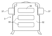
内側シェル3は、筒体31と、筒体31から後方に延出するカバー部32と、カバー部32を折り曲げるための折り曲げ部33と、筒体31から下方に延出した脚部34と、を備えている。
The
カバー部32には、外側シェル5の後方側の内面と接触するように、外面から外方(後方)に膨出するリブ部35(膨出部の一例)が形成されている。本実施形態では、カバー部32の左右両側に、縦長に延びた面状のリブ部35を設けている。詳細は後述するが、外側シェル5を組み付けたとき、このリブ部35が外側シェル5の内面に面接触、つまり内側シェル3と外側シェル5とが大きな面積で接触するので、高周波伝送特性が向上する。また、基板K側で内側シェル3と外側シェル5とを接続させる配線が不要となるので、基板Kのパターン設計の自由度が高くなる。
The
筒体31の側壁の内面には、第2本体2の案内溝22と係合する案内突起38が内方に延出して形成されている。内側シェル3は、第2本体2の前方から案内溝22と案内突起38とを係合させた状態で挿入される。
A
筒体31の側壁の外面には、前後方向の略中央に、外方に膨らんだ膨らみ部36が形成され、第1本体1を内側シェル3に外嵌する際、第1本体1の側壁17の内面に形成した窪みと膨らみ部36とが係合することで案内される。また、筒体31の側壁の後方端部には、当接部37が外方に延出して形成され、第1本体1の第2開口部14aに設けられた規制部14cに当接している。これにより、コネクタC内部で、内側シェル3が前方へ移動することが阻止される。
On the outer surface of the side wall of the
脚部34は、カバー部32の両側端から下方に延出形成されており、基板Kに設けられた孔に挿入される。
The
内側シェル3は、図2、図3の状態では、筒体31の上面と、カバー部32の背面とは略直角に形成されているが、第2本体2に取付けられる前においては、筒体31の上面と、カバー部32の上面とが同一平面上に位置している(二点鎖線の状態)。カバー部32は、内側シェル3の後方からコンタクト4が圧入された第2本体2を嵌合させた後、折り曲げ部33で下方に折り曲げられる。このとき、図5に示すように第2本体2の後方端部26と、内側シェル3のカバー部32の内面とが当接する。
In the state of FIGS. 2 and 3, the
外側シェル5は、第1本体1の被覆部12に、上方から被せられる。外側シェル5は、被覆部12の上面を覆う上面部51と、被覆部12の側壁17を覆う側壁52と、第1本体1および内側シェル3の背面を覆う背面部53と、を備える。
The
外側シェル5の側壁52は、外側シェル5の上面部51の両側端から、下方に延出して形成されている。本実施形態では、同一部材の金属板を曲げ加工することで、上面部51と側壁52とが形成されている。この際、上面部51の両側端は、第1本体1の曲面部12aの形状に沿うように、曲面形状を有している。また、外側シェル5の両側壁52には、前方から順に、第1突片52a、第1脚部52b、第2突片52c、第2脚部52d、固定部52eが形成されている。
The
突片52a,52cは、外側シェル5の側壁52の下端から延出形成されており、外側シェル5を第1本体1に外嵌した後に折り曲げられ。凹部17a,17bと係合して固定される。このとき、凹部17a,17bの上端の規制面17cによって、外側シェル5の上方への変位が規制される。
The projecting
脚部52b,52dは、側壁52の下端から下方に延出形成され、基板Kに設けられた孔に挿入される。
The
固定部52eは、側壁52の後端部の下方に設けられ、内方へ突出する突起として形成されている。
The fixing
外側シェル5の背面部53は、上面部51の後端から下方に延出して形成されている。また、背面部53は、上面部51および側壁52と同一部材の金属板からなり、上面部51の後端で下方に折り曲げられて形成されている。さらに、図3に示すように、背面部53は、側部54と、突出部55と、第3脚部53aとを備える。本実施形態では、図6に示すように、外側シェル5が第1本体1に被せられた際に、背面部53の内面が、内側シェル3のリブ部35と面接触する。
The
側部54は、背面部53の両側端から前方に延出するように折り曲げられて形成されている。また、側部54の下方には、側壁52の固定部52eに固定される被固定部54aが、貫通孔として形成されている。ここに、前述した外側シェル5の側壁52に設けられた突起が入り込み、側壁52と背面部53とが係止固定される。
The
突出部55は、側部54の前方の端部の上方から内方に延出形成されている。本実施形態では、突出部55は、板状の突片として形成されており、側部54の前端で折り曲げられて形成されている。外側シェル5を第1本体1に外嵌する際、突出部55は、前述した第1本体1の溝18に案内される。
The protruding
第3脚部53aは、背面部53の両側端近傍の下端から延出され、脚部52b,52dと同様に、基板Kに設けられた孔に挿入される。
The
次に、コネクタCの組み立て方法を以下に示す。 Next, a method for assembling the connector C will be described below.
まず、上述したように、コンタクト4が第2本体2に組み付けられた後、内側シェル3が第2本体2に外嵌される。そして、第1本体1の第2開口部14aに、一体化された第2本体2及び内側シェル3を挿入する。このとき、図4に示すように、内側シェル3の背面は、第1本体1の背面と同一平面上に位置する。また、図6に示すように、内側シェル3の当接部37が、第1本体1の規制部14cに当接するとともに、第2本体2の当接部27が、第1本体1に当接する。これにより、第2本体2及び内側シェル3の前方への移動が規制される。
First, as described above, after the
図1に示すように、一体化された第2本体2及び内側シェル3を第1本体1に挿入した状態において、コンタクト4の挿入部4bと、内側シェル3の脚部34とは、第1本体1の切欠き14bを通して、コネクタCの下面よりも下方に延出している。また、第1本体1の下面には、下方に突出する底面突起19が設けられている。これらは、基板Kに設けられた孔に挿入される。これにより、第1本体1は基板Kに対して位置決めされるとともに、第1本体1、内側シェル3およびコンタクト4が基板Kに接続される。
As shown in FIG. 1, in a state where the integrated
次に、図4に示すように、外側シェル5を第1本体1の被覆部12に上方から外嵌する。このとき、外側シェル5の突出部55は、溝18に嵌入する。本実施形態では、接続対象の接続方向と直交する方向に溝18が形成されているため、接続対象を挿抜しても、外側シェル5の突出部55が溝18の内面に当接する。このため、外側シェル5が前後方向に変位するのを防ぐことができる。特に、本実施形態では、突出部55が板状の突片で構成され、溝18の内面と面接触するため、外側シェル5と第1本体1とを、より強固に固定することができる。したがって、外側シェル5が第1本体1から抜き出ること防ぐことができる。
Next, as shown in FIG. 4, the
また、本実施形態では、図3に示すように、外側シェル5の背面部53の側端から側部54が延出し、側部54から突出部55が延出しているため、接続対象の挿抜により、突出部55に力が加わっても、力が外側シェル5の側部54および背面部53に分散される。したがって、突出部55の強度が大きいので、外側シェル5が第1本体1から抜け出すことを防ぐことができる。なお、外側シェル5の側部54は、外側シェル5の側壁52に係止固定されているため、外側シェル5の背面部53と側壁52とは固定されている。
Moreover, in this embodiment, as shown in FIG. 3, since the
さらに、外側シェル5を第1本体1に外嵌した後、外側シェル5の側壁52の突片52a,52cが折り曲げられて、第1本体1の凹部17a,17bと係合する。これにより、接続対象を挿抜しても、突片52a,52cが凹部17a,17bの内面に当接し、外側シェル5が第1本体1から前後方向に抜き出ることを防ぐことができる。また、突片52a,52cと規制面17cとが当接し、外側シェル5の上方への変位を規制する。このように、外側シェル5と第1本体1とは強固に固定される。また、外側シェル5を第1本体1へ外嵌すると同時に、外側シェル5の脚部52b,52d,53aが基板Kに設けられた孔へ挿入される。これにより、基板Kと外側シェル5とを固定することができる。
Furthermore, after the
外側シェル5を第1本体1に外嵌した状態において、図5に示すように、第2本体2の後方端部26が内側シェル3のカバー部32の内面に当接すると共に、第2本体2の前方端部25の当接部27が第1本体1に当接する。また、図6に示すように、内側シェル3の当接部37が、第1本体1の規制部14cと当接すると共に、内側シェル3のカバー部32の外面に形成されたリブ部35が、外側シェル5の背面部53の内面と接触する。これらにより、第2本体2及び内側シェル3は、第1本体1及び外側シェル5に位置決めされ、内側シェル3の前方への移動が阻止される。したがって、本体が複数部品からなる場合でも、本体の構成部品同士を固定する部材を設ける必要がないため、構造を簡単にすることができる。
In the state in which the
しかも、外側シェル5を第1本体1に外嵌する際、内側シェル3のカバー部32の外方にリブ部35を設けているので、背面部53が外方(後方)に弾性変形する。その結果、内側シェル3のリブ部35と外側シェル5の背面部53とが強く面接触するので、EMI特性が向上する。また、接続対象を第2本体2に接続した際の押込力が、第2本体2の後方端部26を介して内側シェル3、外側シェル5の順番で伝達される。よって、内側シェル3のリブ部35を弾性変形させるような圧縮力が働いて、リブ部35と背面部53とを強固に接触させることができる。さらに、リブ部35は、接続対象の接続方向に直交する方向であるので、接続対象の押込力が伝達されると共に、上下方向への振動があっても接触不良が生じにくい。なお、このリブ部35は、外側シェル5の背面部53を弾性変形させつつ、内側シェル3と外側シェル5とが確実に接触するように、高さ・位置・大きさが調整されている。
In addition, when the
[その他の実施形態]
(1)上述した実施形態では、カバー部32の左右両側に、縦長に延びた面状のリブ部35を設けたが、図7に示すように、カバー部32の上下方向に横長に延びた面状のリブ部35を複数設けてもよい。つまり、リブ部35の位置、数量、大きさは特に限定されず、内側シェル3の外面と外側シェル5の内面とが面接触で確実に接触する構成であればどのような形態であってもよい。
(2)上述した実施形態では、突出部55は、背面部53から延出された側部54の端部に延出形成されていたが、第1本体1の溝18に嵌入するものであれば、外側シェル5のどこに設けられていてもよい。例えば、外側シェル5の側壁52に設けられていてもよい。
(3)上述した実施形態では、当接部37は、内側シェル3の筒体31の後方端部側から外方に延出形成して第1本体1の規制部14cと当接させたが、内側シェル3の前方移動を規制できるものであれば、どのような形態であってもよい。例えば、内側シェル3の筒体31の後方端部側から内方に延出形成して第2本体2の後方端部と当接させたり、別部材の当接部37を内側シェル3に溶接固定したりしてもよい。
(4)上述した実施形態では、内側シェル3や外側シェル5は単品部材から折り曲げられて形成されていたが、別部材から形成されていてもよい。
(5)上述した実施形態では、外側シェル5の側壁52の固定部52eは突起とし、側部54の被固定部54aは貫通孔として形成されていたが、側壁52と側部54とが係止固定されれば、どのような固定方法でも構わない。また、側壁52と側部54とが係止固定されていなくてもよい。
(6)上述した実施形態では、内側シェル3や外側シェル5に複数の脚部が設けられていたが、脚部の位置や数量は特に限定されず、これらを設けていなくてもよい。また、第1本体1の下面に2つの底面突起19が設けられていたが、底面突起19の数量は特に限定されず、これらを設けなくてもよい。
[Other Embodiments]
(1) In the above-described embodiment, the longitudinally extending
(2) In the above-described embodiment, the protruding
(3) In the above-described embodiment, the
(4) In the above-described embodiment, the
(5) In the above-described embodiment, the fixing
(6) In the above-described embodiment, the
本発明は、接続対象に電気的に接続するコネクタに利用可能である。 The present invention can be used for a connector that is electrically connected to a connection target.
1 第1本体(第二絶縁体)
18 溝
2 第2本体(第一絶縁体)
25 前方端部
26 後方端部
3 内側シェル(第一金属体)
35 リブ部(膨出部)
37 当接部
4 コンタクト
5 外側シェル(第二金属体)
55 突出部
C コネクタ
1 First body (second insulator)
18
25
35 Rib part (bulging part)
37
55 Protrusion C Connector
Claims (5)
前記接続対象が接続される前方端部とこの前方端部に対向する後方端部とを有し、前記コンタクトを保持する第一絶縁体と、
前記第一絶縁体を覆う第一金属体と、
前記第一金属体を保持する第二絶縁体と、
前記第一金属体及び前記第二絶縁体を覆う第二金属体と、を備え、
前記第一金属体は、前記後方端部側の外面から外方に膨出した膨出部を形成することにより前記第二金属体と接触しているコネクタ。 A contact that is electrically connected to the connection object;
A first insulator having a front end to which the connection target is connected and a rear end facing the front end, and holding the contact;
A first metal body covering the first insulator;
A second insulator holding the first metal body;
A second metal body covering the first metal body and the second insulator,
The first metal body is a connector that is in contact with the second metal body by forming a bulging portion that bulges outward from an outer surface on the rear end side.
前記第二金属体は、内方に突出する突出部を有し、
前記突出部は、前記溝に嵌入される請求項1又は2に記載のコネクタ。 The second insulator has a groove formed in a direction orthogonal to the connection direction of the connection target,
The second metal body has a protruding portion protruding inwardly,
The connector according to claim 1, wherein the protruding portion is fitted into the groove.
前記当接部が前記第二絶縁体に当接することで、前記第一金属体の前記前方端部側への移動が阻止される請求項1から3のいずれか一項に記載のコネクタ。 A contact portion that contacts the second insulator while being sandwiched between the second insulator and the second metal body is formed on the rear end side of the first metal body,
The connector according to any one of claims 1 to 3, wherein the first metal body is prevented from moving toward the front end portion by the contact of the contact portion with the second insulator.
前記当接部は、前記第一金属体の前記後方端部側から外方に延出して形成される請求項4に記載のコネクタ。 The second insulator is externally fitted to the first metal body from the connection direction of the connection target,
The connector according to claim 4, wherein the contact portion is formed to extend outward from the rear end portion side of the first metal body.
Priority Applications (4)
| Application Number | Priority Date | Filing Date | Title |
|---|---|---|---|
| JP2014050120A JP2015176657A (en) | 2014-03-13 | 2014-03-13 | connector |
| EP15156652.8A EP2919329B1 (en) | 2014-03-13 | 2015-02-26 | Connector |
| US14/643,744 US9401567B2 (en) | 2014-03-13 | 2015-03-10 | Connector having a first metal member with a bulging portion contacting a second metal member |
| CN201510108101.5A CN104916995B (en) | 2014-03-13 | 2015-03-12 | Connector |
Applications Claiming Priority (1)
| Application Number | Priority Date | Filing Date | Title |
|---|---|---|---|
| JP2014050120A JP2015176657A (en) | 2014-03-13 | 2014-03-13 | connector |
Publications (1)
| Publication Number | Publication Date |
|---|---|
| JP2015176657A true JP2015176657A (en) | 2015-10-05 |
Family
ID=52577744
Family Applications (1)
| Application Number | Title | Priority Date | Filing Date |
|---|---|---|---|
| JP2014050120A Pending JP2015176657A (en) | 2014-03-13 | 2014-03-13 | connector |
Country Status (4)
| Country | Link |
|---|---|
| US (1) | US9401567B2 (en) |
| EP (1) | EP2919329B1 (en) |
| JP (1) | JP2015176657A (en) |
| CN (1) | CN104916995B (en) |
Cited By (9)
| Publication number | Priority date | Publication date | Assignee | Title |
|---|---|---|---|---|
| JP2017045604A (en) * | 2015-08-26 | 2017-03-02 | タイコエレクトロニクスジャパン合同会社 | Shield connector |
| JP2017098154A (en) * | 2015-11-26 | 2017-06-01 | 日本圧着端子製造株式会社 | Shield connector |
| KR20170072756A (en) * | 2015-12-17 | 2017-06-27 | 한국단자공업 주식회사 | Connector |
| JP2018045967A (en) * | 2016-09-16 | 2018-03-22 | 日本航空電子工業株式会社 | connector |
| JP2018137158A (en) * | 2017-02-23 | 2018-08-30 | 日本航空電子工業株式会社 | Board mounting connector |
| WO2019009048A1 (en) * | 2017-07-05 | 2019-01-10 | 株式会社オートネットワーク技術研究所 | Connection structure for circuit board and substrate connector, and substrate connector |
| JP2019129117A (en) * | 2018-01-26 | 2019-08-01 | 住友電装株式会社 | Shield connector |
| JP2020161214A (en) * | 2019-03-25 | 2020-10-01 | ヒロセ電機株式会社 | Connector and connector device |
| JP2022125847A (en) * | 2021-02-17 | 2022-08-29 | 日本航空電子工業株式会社 | shielded connector |
Families Citing this family (9)
| Publication number | Priority date | Publication date | Assignee | Title |
|---|---|---|---|---|
| JP6078919B2 (en) * | 2013-07-18 | 2017-02-15 | ホシデン株式会社 | connector |
| US10283915B2 (en) * | 2015-05-07 | 2019-05-07 | Samsung Electronics Co., Ltd | Connector and electronic device including the same |
| KR102283147B1 (en) * | 2015-05-07 | 2021-07-30 | 삼성전자주식회사 | A Connector and Electronic Device Equipped with the Connector |
| US9425558B1 (en) * | 2015-10-22 | 2016-08-23 | Cheng Uei Precision Industry Co., Ltd. | Electrical connector having an outer shielding covered by a cover with a resilient plate extending upward and rearward |
| USD873219S1 (en) * | 2017-04-12 | 2020-01-21 | Hosiden Corporation | Electric connector |
| CN107623200A (en) * | 2017-10-23 | 2018-01-23 | 安费诺(常州)高端连接器有限公司 | Orthogonal staggeredly crimping back panel connector |
| JP7288757B2 (en) * | 2018-12-24 | 2023-06-08 | ロベルト・ボッシュ・ゲゼルシャフト・ミト・ベシュレンクテル・ハフツング | adapter |
| CN216672088U (en) * | 2021-12-31 | 2022-06-03 | 泰科电子科技(苏州工业园区)有限公司 | Shield and connector |
| DE102023108134A1 (en) * | 2023-03-30 | 2024-10-02 | Md Elektronik Gmbh | CONNECTORS, CONNECTOR SYSTEMS AND TRANSMISSION METHODS |
Citations (4)
| Publication number | Priority date | Publication date | Assignee | Title |
|---|---|---|---|---|
| JPH08306435A (en) * | 1995-04-28 | 1996-11-22 | Mitsumi Electric Co Ltd | Electrical connector |
| JP3109294U (en) * | 2004-12-13 | 2005-05-19 | 正▲うえ▼精密工業股▲ふん▼有限公司 | Connector with shield |
| JP2009193858A (en) * | 2008-02-15 | 2009-08-27 | Yazaki Corp | Shield connector |
| JP2013058357A (en) * | 2011-09-07 | 2013-03-28 | Yazaki Corp | Shield connector |
Family Cites Families (11)
| Publication number | Priority date | Publication date | Assignee | Title |
|---|---|---|---|---|
| JP4082707B2 (en) * | 2005-04-28 | 2008-04-30 | 日本航空電子工業株式会社 | connector |
| JP4987646B2 (en) | 2007-09-14 | 2012-07-25 | 日本圧着端子製造株式会社 | Double structure electrical connector |
| JP5160970B2 (en) * | 2008-06-16 | 2013-03-13 | 矢崎総業株式会社 | Shield connector |
| US20100003852A1 (en) * | 2008-07-07 | 2010-01-07 | Tyco Electronics Corporation | Electrical connector with improved grounding |
| CN201252259Y (en) * | 2008-07-24 | 2009-06-03 | 富士康(昆山)电脑接插件有限公司 | Electrical connector |
| CN201285934Y (en) * | 2008-08-05 | 2009-08-05 | 富士康(昆山)电脑接插件有限公司 | Electric connector |
| CN102623848B (en) * | 2011-01-28 | 2014-09-24 | 富士康(昆山)电脑接插件有限公司 | electrical connector |
| JP5696698B2 (en) * | 2012-08-23 | 2015-04-08 | Smk株式会社 | Receptacle connector |
| US8961230B2 (en) * | 2012-10-04 | 2015-02-24 | Ezconn Corporation | Connector |
| CN203367652U (en) * | 2013-05-31 | 2013-12-25 | 富士康(昆山)电脑接插件有限公司 | Stack electric connector |
| JP6078919B2 (en) * | 2013-07-18 | 2017-02-15 | ホシデン株式会社 | connector |
-
2014
- 2014-03-13 JP JP2014050120A patent/JP2015176657A/en active Pending
-
2015
- 2015-02-26 EP EP15156652.8A patent/EP2919329B1/en not_active Not-in-force
- 2015-03-10 US US14/643,744 patent/US9401567B2/en not_active Expired - Fee Related
- 2015-03-12 CN CN201510108101.5A patent/CN104916995B/en not_active Expired - Fee Related
Patent Citations (4)
| Publication number | Priority date | Publication date | Assignee | Title |
|---|---|---|---|---|
| JPH08306435A (en) * | 1995-04-28 | 1996-11-22 | Mitsumi Electric Co Ltd | Electrical connector |
| JP3109294U (en) * | 2004-12-13 | 2005-05-19 | 正▲うえ▼精密工業股▲ふん▼有限公司 | Connector with shield |
| JP2009193858A (en) * | 2008-02-15 | 2009-08-27 | Yazaki Corp | Shield connector |
| JP2013058357A (en) * | 2011-09-07 | 2013-03-28 | Yazaki Corp | Shield connector |
Cited By (15)
| Publication number | Priority date | Publication date | Assignee | Title |
|---|---|---|---|---|
| JP2017045604A (en) * | 2015-08-26 | 2017-03-02 | タイコエレクトロニクスジャパン合同会社 | Shield connector |
| JP2017098154A (en) * | 2015-11-26 | 2017-06-01 | 日本圧着端子製造株式会社 | Shield connector |
| KR20170072756A (en) * | 2015-12-17 | 2017-06-27 | 한국단자공업 주식회사 | Connector |
| KR102499819B1 (en) * | 2015-12-17 | 2023-02-15 | 한국단자공업 주식회사 | Connector |
| JP2018045967A (en) * | 2016-09-16 | 2018-03-22 | 日本航空電子工業株式会社 | connector |
| US10978817B2 (en) | 2017-02-23 | 2021-04-13 | Japan Aviation Electronics Industry, Limited | Connector for mounting to a substrate |
| WO2018155330A1 (en) * | 2017-02-23 | 2018-08-30 | 日本航空電子工業株式会社 | Connector for base board mounting use |
| JP2018137158A (en) * | 2017-02-23 | 2018-08-30 | 日本航空電子工業株式会社 | Board mounting connector |
| WO2019009048A1 (en) * | 2017-07-05 | 2019-01-10 | 株式会社オートネットワーク技術研究所 | Connection structure for circuit board and substrate connector, and substrate connector |
| US11329415B2 (en) | 2017-07-05 | 2022-05-10 | Autonetworks Technologies, Ltd. | Connection structure for circuit board and board connector, and board connector |
| JP2019129117A (en) * | 2018-01-26 | 2019-08-01 | 住友電装株式会社 | Shield connector |
| JP2020161214A (en) * | 2019-03-25 | 2020-10-01 | ヒロセ電機株式会社 | Connector and connector device |
| JP7008659B2 (en) | 2019-03-25 | 2022-01-25 | ヒロセ電機株式会社 | Connector and connector device |
| JP2022125847A (en) * | 2021-02-17 | 2022-08-29 | 日本航空電子工業株式会社 | shielded connector |
| JP7522680B2 (en) | 2021-02-17 | 2024-07-25 | 日本航空電子工業株式会社 | Shielded Connectors |
Also Published As
| Publication number | Publication date |
|---|---|
| CN104916995B (en) | 2019-04-26 |
| CN104916995A (en) | 2015-09-16 |
| US9401567B2 (en) | 2016-07-26 |
| EP2919329A1 (en) | 2015-09-16 |
| EP2919329B1 (en) | 2018-06-27 |
| US20150263457A1 (en) | 2015-09-17 |
Similar Documents
| Publication | Publication Date | Title |
|---|---|---|
| JP2015176657A (en) | connector | |
| US7658654B2 (en) | Female terminal fitting | |
| CN102394428B (en) | Circuit board mounted connector | |
| US8979584B2 (en) | Board-mounted connector | |
| TWI596840B (en) | Electrical connectors | |
| JP6538134B2 (en) | connector | |
| JP6996445B2 (en) | Shielded connector and outer conductor terminal | |
| JP6078919B2 (en) | connector | |
| US10276989B2 (en) | Electrical connector with intimate side arms extending from metallic shell and integrally formed within insulative shell | |
| JP2019117692A (en) | L-shaped electric connector for circuit board and manufacturing method thereof | |
| EP3467948B1 (en) | Connector | |
| WO2020017572A1 (en) | Connector and outer conductor | |
| JP2017123223A (en) | Connector and connector assembly | |
| JP2007193949A (en) | connector | |
| JP4175655B2 (en) | Connector with shell | |
| JP5229722B2 (en) | Floating connector | |
| JP2022107105A (en) | Connector and connector device | |
| JP5700807B2 (en) | connector | |
| US9793655B2 (en) | Electrical connector with expanded housing to form mating cavity with offset EMI springs | |
| CN110233370A (en) | Terminal, connector and electrical connector | |
| JP5105195B2 (en) | connector | |
| JP2019145463A (en) | connector | |
| JP2019096426A (en) | Joint terminal | |
| JP2023111007A (en) | shield connector | |
| WO2024253079A1 (en) | Substrate connector |
Legal Events
| Date | Code | Title | Description |
|---|---|---|---|
| A621 | Written request for application examination |
Free format text: JAPANESE INTERMEDIATE CODE: A621 Effective date: 20161013 |
|
| A977 | Report on retrieval |
Free format text: JAPANESE INTERMEDIATE CODE: A971007 Effective date: 20170608 |
|
| A131 | Notification of reasons for refusal |
Free format text: JAPANESE INTERMEDIATE CODE: A131 Effective date: 20170620 |
|
| A521 | Request for written amendment filed |
Free format text: JAPANESE INTERMEDIATE CODE: A523 Effective date: 20170807 |
|
| A02 | Decision of refusal |
Free format text: JAPANESE INTERMEDIATE CODE: A02 Effective date: 20180109 |