JP2011249401A - Method for manufacturing semiconductor laser - Google Patents

Method for manufacturing semiconductor laser Download PDF

Info

Publication number
JP2011249401A
JP2011249401A JP2010118347A JP2010118347A JP2011249401A JP 2011249401 A JP2011249401 A JP 2011249401A JP 2010118347 A JP2010118347 A JP 2010118347A JP 2010118347 A JP2010118347 A JP 2010118347A JP 2011249401 A JP2011249401 A JP 2011249401A
Authority
JP
Japan
Prior art keywords
semiconductor laser
scribe groove
semiconductor
laser bar
region
Prior art date
Legal status (The legal status is an assumption and is not a legal conclusion. Google has not performed a legal analysis and makes no representation as to the accuracy of the status listed.)
Pending
Application number
JP2010118347A
Other languages
Japanese (ja)
Inventor
Toshiyuki Yamamoto
敏之 山本
Current Assignee (The listed assignees may be inaccurate. Google has not performed a legal analysis and makes no representation or warranty as to the accuracy of the list.)
Hamamatsu Photonics KK
Original Assignee
Hamamatsu Photonics KK
Priority date (The priority date is an assumption and is not a legal conclusion. Google has not performed a legal analysis and makes no representation as to the accuracy of the date listed.)
Filing date
Publication date
Application filed by Hamamatsu Photonics KK filed Critical Hamamatsu Photonics KK
Priority to JP2010118347A priority Critical patent/JP2011249401A/en
Publication of JP2011249401A publication Critical patent/JP2011249401A/en
Pending legal-status Critical Current

Links

Images

Landscapes

  • Semiconductor Lasers (AREA)

Abstract

PROBLEM TO BE SOLVED: To provide a method for easily manufacturing a semiconductor laser having a plurality of light-emitting regions without causing reduction in yield.SOLUTION: The method for manufacturing a semiconductor laser includes a step for forming a semiconductor laser bar 1a, a step for forming a scribe groove 5a in a surface S3 of a substrate, a step for mounting a semiconductor laser bar 1b in which the scribe groove 5a is formed on a sub-mount 11, and a step for separating a plurality of semiconductor lasers 1 from the semiconductor laser bar 1b along the scribe groove 5a. The surface S3 extends along the longitudinal direction of the sub-mount 11 and has a region 13 where the scribe groove 5a is not formed. Mechanical strength of the semiconductor laser bar 1b is enhanced by providing the region 13 where the scribe groove 5a is not formed.

Description

本発明は、半導体レーザ装置の製造方法に関する。   The present invention relates to a method for manufacturing a semiconductor laser device.

特許文献1には、半導体基板上に複数のレーザ発光領域を有する多層成長層を形成した半導体レーザ装置及びその製造方法が開示されている。特許文献1には、まず、発光領域間に半導体基板の深部にまで至る分割溝を形成し、次に半導体レーザアレイを線膨張率の異なるベース材上に接合したときに発生する熱応力や接合後に発生させる反りを利用して分割溝先端部から亀裂を進展させて分割することによって、半導体レーザアレイが受ける大きな熱応力を低減し、従来必要であった応力緩和材を排除し、更に、半導体レーザアレイの破損を回避するための半導体レーザアレイの製造方法が開示されている。   Patent Document 1 discloses a semiconductor laser device in which a multilayer growth layer having a plurality of laser emission regions is formed on a semiconductor substrate, and a manufacturing method thereof. In Patent Document 1, first, a dividing groove extending to the deep part of the semiconductor substrate is formed between the light emitting regions, and then the thermal stress or bonding generated when the semiconductor laser array is bonded onto the base material having a different linear expansion coefficient. By using the warp that is generated later, cracks are propagated from the tip of the split groove and split to reduce the large thermal stress received by the semiconductor laser array, eliminating the stress relieving material that was required in the past, and semiconductors A method of manufacturing a semiconductor laser array for avoiding damage to the laser array is disclosed.

特開平11−220204号公報Japanese Patent Laid-Open No. 11-220204

特許文献1の製造方法において、発光領域間に半導体基板の深部にまで至るように形成された分割溝は、発光領域の両端のそれぞれ形成されている半導体基板の一の側面から他の側面まで連続して形成される。このように、分割溝が、一の側面から他の側面まで連続して形成されている場合、この分割溝によって半導体基板の機械的強度は低くなる。半導体基板には複数の分割溝が形成されているので、半導体基板の機械的強度は、分割溝の数に応じてさらに低減される。従って、半導体基板をベース材に実装する前に、半導体基板がこの分割溝を境に分離されるおそれがあり、歩留まりが低下する。また、半導体基板の取り扱いは、ベース材への実装前において特に困難となり、作業性の低下をも招く。そこで、本発明の目的は、歩留まりの低下を招くことなく複数の発光領域を有する半導体レーザ装置を容易に製造する方法を提供することである。   In the manufacturing method of Patent Document 1, the division grooves formed so as to reach the deep part of the semiconductor substrate between the light emitting regions are continuous from one side surface to the other side surface of the semiconductor substrate respectively formed at both ends of the light emitting region. Formed. As described above, when the dividing groove is continuously formed from one side surface to the other side surface, the mechanical strength of the semiconductor substrate is lowered by the dividing groove. Since the semiconductor substrate has a plurality of dividing grooves, the mechanical strength of the semiconductor substrate is further reduced according to the number of dividing grooves. Therefore, before the semiconductor substrate is mounted on the base material, the semiconductor substrate may be separated at the dividing groove, and the yield is reduced. In addition, handling of the semiconductor substrate becomes particularly difficult before mounting on the base material, which leads to a decrease in workability. Accordingly, an object of the present invention is to provide a method for easily manufacturing a semiconductor laser device having a plurality of light emitting regions without causing a decrease in yield.

本発明に係る半導体レーザを製造する製造方法は、基板と、複数の発光領域を含む上記基板上の半導体積層部と、を有する半導体レーザバーから、複数の半導体レーザを有する半導体レーザ装置を製造する製造方法であって、上記半導体レーザバーを形成する工程と、上記基板の表面にスクライブ溝を形成する工程と、上記半導体レーザバーを上記サブマウント上に搭載する工程と、上記複数の半導体レーザを、上記スクライブ溝に沿って上記半導体レーザバーから分離する工程と、を備え、上記半導体レーザバーを上記サブマウント上に搭載する工程では、上記半導体積層部が上記基板と上記サブマウントとの間に配置されるように上記半導体レーザバーを上記サブマウント上に搭載し、上記発光領域は、上記半導体積層部の側面と交差する方向に延びており、上記スクライブ溝は、上記発光領域と並行して延びていると共に、上記表面側からみて、隣接している二つの上記発光領域の間にあり、上記表面は、上記側面に沿って延びており上記スクライブ溝の形成されない領域を有する、ことを特徴とする。   A manufacturing method for manufacturing a semiconductor laser according to the present invention is a manufacturing method for manufacturing a semiconductor laser device having a plurality of semiconductor lasers from a semiconductor laser bar having a substrate and a semiconductor stacked portion on the substrate including a plurality of light emitting regions. A step of forming the semiconductor laser bar; a step of forming a scribe groove on a surface of the substrate; a step of mounting the semiconductor laser bar on the submount; and the plurality of semiconductor lasers. Separating the semiconductor laser bar from the semiconductor laser bar along a groove, and in the step of mounting the semiconductor laser bar on the submount, the semiconductor stacked portion is disposed between the substrate and the submount. The semiconductor laser bar is mounted on the submount, and the light emitting region intersects with a side surface of the semiconductor stacked portion. The scribe groove extends in parallel with the light emitting region, and is located between two adjacent light emitting regions when viewed from the surface side, and the surface is formed on the side surface. It has the area | region extended along and the said scribe groove | channel is not formed, It is characterized by the above-mentioned.

このように、基板の表面は、半導体積層部の側面に沿って延びておりスクライブ溝の形成されない領域を有するので、スクライブ溝の形成後の半導体レーザバーの機械的強度は、基板の表面にこのような領域が設けられておらず表面の一端から他端に至るまで連続した形状でスクライブ溝が形成されている半導体レーザバーに比較して、向上される。半導体レーザバーの機械的強度が向上されることにより、半導体レーザバーを用いて製造される半導体レーザ装置の歩留まりが向上される。   As described above, since the surface of the substrate has a region where the scribe groove is not formed and extends along the side surface of the semiconductor stacked portion, the mechanical strength of the semiconductor laser bar after the formation of the scribe groove can be reduced in this manner on the surface of the substrate. This is an improvement over a semiconductor laser bar in which a scribe groove is formed in a continuous shape from one end of the surface to the other end without a special region. By improving the mechanical strength of the semiconductor laser bar, the yield of the semiconductor laser device manufactured using the semiconductor laser bar is improved.

本発明に係る半導体レーザを製造する製造方法では、上記スクライブ溝の形成されない領域の幅は、上記半導体レーザバーの厚みよりも小さい、とすることができる。このように、スクライブ溝の形成されない領域の幅は半導体レーザバーの厚みよりも小さいので、スクライブ溝の形成されていない領域を確保しつつ十分に長いスクライブ溝を形成できる。従って、半導体レーザバーの機械的強度が十分に確保できるとともにスクライブ溝に沿った半導体レーザの分離も良好に行える。   In the manufacturing method for manufacturing the semiconductor laser according to the present invention, the width of the region where the scribe groove is not formed can be smaller than the thickness of the semiconductor laser bar. Thus, since the width of the region where the scribe groove is not formed is smaller than the thickness of the semiconductor laser bar, a sufficiently long scribe groove can be formed while securing the region where the scribe groove is not formed. Therefore, the mechanical strength of the semiconductor laser bar can be sufficiently secured and the semiconductor laser can be well separated along the scribe groove.

本発明に係る半導体レーザを製造する製造方法では、上記表面は、上記側面に沿って延びている端部を有し、上記スクライブ溝の形成されない領域は、上記端部を含んでいる、とすることができるし、又は、上記表面は、上記側面に沿って延びている端部を有し、上記スクライブ溝の形成されない領域は、上記端部よりも内側において延在している、ことができる。このように、スクライブ溝が形成されない領域は、基板の表面の端部を含むように設けてもよいし、基板の表面の端部を含まないように設けてもよい。   In the manufacturing method for manufacturing a semiconductor laser according to the present invention, the surface has an end extending along the side surface, and the region where the scribe groove is not formed includes the end. Or the surface may have an end extending along the side surface, and the region where the scribe groove is not formed may extend inside the end. . As described above, the region where the scribe groove is not formed may be provided so as to include an end portion of the surface of the substrate, or may be provided so as not to include an end portion of the surface of the substrate.

本発明によれば、歩留まりの低下を招くことなく複数の発光領域を有する半導体レーザ装置を容易に製造できる。   According to the present invention, it is possible to easily manufacture a semiconductor laser device having a plurality of light emitting regions without causing a decrease in yield.

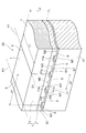
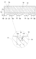
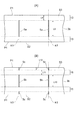
図1は、実施形態に係る半導体レーザ装置の構成を示す図である。FIG. 1 is a diagram illustrating a configuration of a semiconductor laser device according to an embodiment. 図2は、実施形態に係る半導体レーザ装置の製造方法を説明するためのフローチャートである。FIG. 2 is a flowchart for explaining the method for manufacturing the semiconductor laser device according to the embodiment. 図3は、実施形態に係る半導体レーザ装置の製造に用いる半導体レーザバーの構成を示す図である。FIG. 3 is a diagram showing a configuration of a semiconductor laser bar used for manufacturing the semiconductor laser device according to the embodiment. 図4は、実施形態に係る半導体レーザバーの断面構成を示す図である。FIG. 4 is a diagram illustrating a cross-sectional configuration of the semiconductor laser bar according to the embodiment. 図5は、実施形態に係る半導体レーザバーに形成されるスクライブ溝の構成を示す図である。FIG. 5 is a diagram illustrating a configuration of a scribe groove formed in the semiconductor laser bar according to the embodiment. 図6は、実施形態に係る半導体レーザバーがサブマウントに搭載される様子を示す図である。FIG. 6 is a diagram illustrating a state in which the semiconductor laser bar according to the embodiment is mounted on the submount. 図7は、実施形態に係る半導体レーザ装置の製造方法によって、半導体レーザの反りが低減された様子を示すグラフである。FIG. 7 is a graph showing a state in which the warpage of the semiconductor laser is reduced by the method for manufacturing the semiconductor laser device according to the embodiment.

以下、図面を参照して、本発明に係る好適な実施形態について詳細に説明する。なお、図面の説明において、可能な場合には、同一要素には同一符号を付し、重複する説明を省略する。図1は、本実施形態に係る半導体レーザ装置30の概観を示す図である。半導体レーザ装置30は、複数の半導体レーザ1と、サブマウント11とを備える。   Hereinafter, preferred embodiments of the present invention will be described in detail with reference to the drawings. In the description of the drawings, if possible, the same elements are denoted by the same reference numerals, and redundant description is omitted. FIG. 1 is a diagram showing an overview of a semiconductor laser device 30 according to the present embodiment. The semiconductor laser device 30 includes a plurality of semiconductor lasers 1 and a submount 11.

半導体レーザ1は、サブマウント11の表面11a上に設けられている。隣接する二つの半導体レーザ1は、境界面5を介して、隣接している。複数の半導体レーザ1は、サブマウント11の表面11a上において境界面5に交差する向きに並んで配置されている。半導体レーザ1は、境界面5に交差して延びている側面S1を有する。半導体レーザ1は、側面S1の反対側にある他の側面を有し、この側面も境界面5に交差して延びている(側面S1に並行に延びている)。半導体レーザ1は、基板3と半導体積層部7とを有する。   The semiconductor laser 1 is provided on the surface 11 a of the submount 11. Two adjacent semiconductor lasers 1 are adjacent to each other through a boundary surface 5. The plurality of semiconductor lasers 1 are arranged side by side in a direction intersecting the boundary surface 5 on the surface 11 a of the submount 11. The semiconductor laser 1 has a side surface S <b> 1 that extends across the boundary surface 5. The semiconductor laser 1 has another side surface opposite to the side surface S1, and this side surface also extends across the boundary surface 5 (extends in parallel with the side surface S1). The semiconductor laser 1 has a substrate 3 and a semiconductor laminated portion 7.

半導体積層部7は、基板3上に複数の半導体層を成長させ積層することで形成されている。図1に示す半導体レーザ1の半導体積層部7は、二つのメサ部M1を有する。この半導体積層部7が有するメサ部M1の数は、一つであってもよいし、三つ以上であってもよい。半導体積層部7のメサ部M1の表面には図示しない電極が形成され、半田部9を介してサブマウント11上に設けられている。半田部9は、半導体積層部7のメサ部M1表面の電極とサブマウント11の表面11aとの間に設けられている。半導体積層部7のメサ部M1の間には、凹部が形成されており、半田部9はメサ部M1間の領域(凹部)上には設けられていない。半導体レーザ1の複数のメサ部M1は、それぞれ発光領域M2を有する。各発光領域M2は、境界面5と並行に延びている。   The semiconductor laminated portion 7 is formed by growing and laminating a plurality of semiconductor layers on the substrate 3. The semiconductor stacked portion 7 of the semiconductor laser 1 shown in FIG. 1 has two mesa portions M1. The number of mesa portions M1 included in the semiconductor stacked portion 7 may be one or three or more. An electrode (not shown) is formed on the surface of the mesa portion M <b> 1 of the semiconductor laminated portion 7, and is provided on the submount 11 via the solder portion 9. The solder part 9 is provided between the electrode on the surface of the mesa part M <b> 1 of the semiconductor laminated part 7 and the surface 11 a of the submount 11. A recess is formed between the mesa portions M1 of the semiconductor laminated portion 7, and the solder portion 9 is not provided on a region (recess) between the mesa portions M1. Each of the plurality of mesas M1 of the semiconductor laser 1 has a light emitting region M2. Each light emitting area M <b> 2 extends in parallel with the boundary surface 5.

半導体積層部7は、複数のメサ部M1の並ぶ方向に沿って、対向する2つの側面(端面)を有し、一方の側面S1(端面)には発光領域M2から放出される光の一部を反射し残りを透過する反射膜が形成され、一方の側面S1に対向する他方の側面(端面)には発光領域M2から放出される光に対して一方の側面S1に形成された反射膜より高い反射率を有する反射膜が形成されている。半導体積層部7の一方の側面、及びそれに対向する他方の側面にそれぞれ形成された反射膜が共振器を構成することにより、発光領域M2で発生した光が側面S1と対向する側面との間で繰返し反射され、発光領域M2内部でレーザ増幅されて一方の側面(端面)S1からレーザ光が放出される。従って発光領域M2は、半導体積層部7内にあって、側面S1に交差する方向(サブマウント11の長手方向に交差する方向)に延びているということができる。また、発光領域M2は、側面S1から側面S1の反対側(対向する側)にある半導体レーザ1の他の側面まで延びている。発光領域M2の発光点は、側面S1に形成されている。この発光点は発光領域M2の一の端部であり、レーザ光はこの発光点から出射される。なお、上記説明では、側面S1に対向する側の他方の側面には発光領域M2から放出される光に対して一方の側面S1に形成された反射膜より高い反射率を有する反射膜が形成されているとしたが、対向する2つの側面に同反射率を持つ反射膜を形成する場合もある。   The semiconductor stacked portion 7 has two side surfaces (end surfaces) facing each other along the direction in which the plurality of mesa portions M1 are arranged, and a part of light emitted from the light emitting region M2 is provided on one side surface S1 (end surface). Is formed on the other side surface (end surface) opposite to one side surface S1 with respect to the light emitted from the light emitting region M2 than the reflective film formed on one side surface S1. A reflective film having a high reflectance is formed. The reflection films formed on one side surface of the semiconductor stacked portion 7 and the other side surface facing the semiconductor stack portion 7 constitute a resonator, so that the light generated in the light emitting region M2 is between the side surface facing the side surface S1. The light is repeatedly reflected, laser amplified within the light emitting region M2, and laser light is emitted from one side surface (end surface) S1. Therefore, it can be said that the light emitting region M2 is in the semiconductor stacked portion 7 and extends in the direction intersecting the side surface S1 (direction intersecting the longitudinal direction of the submount 11). The light emitting region M2 extends from the side surface S1 to the other side surface of the semiconductor laser 1 on the opposite side (opposite side) of the side surface S1. The light emitting point of the light emitting region M2 is formed on the side surface S1. This light emitting point is one end of the light emitting region M2, and the laser light is emitted from this light emitting point. In the above description, a reflection film having a higher reflectance than the reflection film formed on one side S1 is formed on the other side opposite to the side S1 with respect to the light emitted from the light emitting region M2. However, there may be a case where a reflective film having the same reflectance is formed on two opposing side surfaces.

基準線K1は、側面S1と、側面S1の反対側(対向する側)にある半導体レーザ1の他の側面とに交差する方向に延びており、境界面5に並行に延びている。また、基準線K1は、境界面5に重なっており、隣接する二つの半導体レーザ1のそれぞれの基板3の表面間に位置しているものとする。複数の半導体レーザ1は、サブマウント11の表面11a上において基準線K1に交差する向きに並んでいるということができる。また発光領域M2は、基準線K1に並行に延びているということができる。   The reference line K1 extends in a direction intersecting the side surface S1 and the other side surface of the semiconductor laser 1 on the opposite side (opposite side) of the side surface S1, and extends in parallel with the boundary surface 5. Further, it is assumed that the reference line K1 overlaps the boundary surface 5 and is located between the surfaces of the substrates 3 of the two adjacent semiconductor lasers 1. It can be said that the plurality of semiconductor lasers 1 are arranged on the surface 11a of the submount 11 in a direction intersecting the reference line K1. Further, it can be said that the light emitting region M2 extends in parallel to the reference line K1.

半導体レーザ1の長さL1(側面S1から、側面S1の反対側(対向する側)にある半導体レーザ1の他の側面までの長さ)は、例えば950μm以上1050μm以下であり、1000μm程度であることができる。長さL1は、共振器長(発光領域M2の長さ)に対応する。また半導体レーザ1の厚みL2は、例えば、130μm以上150μm以下である。具体的には140μm程度の基板3上に、数μm程度で半導体積層部7が積層されているので、厚みL2は、概ね140μmに数μmを加えた程度の値であることができる。半導体レーザ1の隣接する二つのメサ部M1間の長さL3は、例えば40μm以上60μm以下であり、50μm程度であることができる。長さL3は、隣接する二つのメサ部M1間に設けられている凹部(以下、単に凹部という)の幅であるということができる。半導体レーザ1の幅L4は、例えば450μm以上550μm以下であり、500μm程度であることができる。幅L4は、隣接する二つの境界面5間の長さである。隣接する二つの凹部間の長さL5は、例えば240μm以上260μm以下であり、250μm程度であることができる。長さL5は、幅L4が略二等分された値となる。   The length L1 of the semiconductor laser 1 (the length from the side surface S1 to the other side surface of the semiconductor laser 1 on the opposite side (opposite side) of the side surface S1) is, for example, 950 μm or more and 1050 μm or less, and about 1000 μm. be able to. The length L1 corresponds to the resonator length (the length of the light emitting region M2). The thickness L2 of the semiconductor laser 1 is, for example, 130 μm or more and 150 μm or less. Specifically, since the semiconductor laminated portion 7 is laminated on the substrate 3 of about 140 μm with a thickness of about several μm, the thickness L2 can be a value obtained by adding several μm to about 140 μm. The length L3 between two adjacent mesa portions M1 of the semiconductor laser 1 is, for example, not less than 40 μm and not more than 60 μm, and can be about 50 μm. It can be said that the length L3 is the width of a concave portion (hereinafter simply referred to as a concave portion) provided between two adjacent mesa portions M1. The width L4 of the semiconductor laser 1 is, for example, not less than 450 μm and not more than 550 μm, and can be about 500 μm. The width L4 is a length between two adjacent boundary surfaces 5. A length L5 between two adjacent recesses is, for example, not less than 240 μm and not more than 260 μm, and can be about 250 μm. The length L5 is a value obtained by substantially dividing the width L4 into two equal parts.

基板3及び半導体積層部7は、例えばGaAs(ヒ化ガリウム)を含む化合物半導体の材料からなる。GaAsは、6.0×10⁻⁶/K程度の熱膨張率を有することが知られている。半田部9は、例えばAu/Sn(金と錫を含む合金)であるが、In(インジウム)であることもできる。Au/Snは、摂氏280度程度の融点を有し、Inは、摂氏156度程度の融点を有することが知られている。サブマウント11は、例えばAlN(窒化アルミニウム)を材料に含むが、AlNに替えて、Cu(銅)、CuW(銅タングステン)の何れかを材料に含むことができる。AlNは、4.5×10−6/K程度の熱膨張率を有し、Cuは、17×10−6/K程度の熱膨張率を有し、CuWは、6.5×10−6/K程度の熱膨張率を有することが、知られている。 The substrate 3 and the semiconductor stacked portion 7 are made of a compound semiconductor material containing, for example, GaAs (gallium arsenide). GaAs is known to have a coefficient of thermal expansion of about 6.0 × 10 −6 / K. The solder portion 9 is, for example, Au / Sn (an alloy containing gold and tin), but can also be In (indium). It is known that Au / Sn has a melting point of about 280 degrees Celsius, and In has a melting point of about 156 degrees Celsius. The submount 11 includes, for example, AlN (aluminum nitride) as a material, but can include Cu (copper) or CuW (copper tungsten) as a material instead of AlN. AlN has a coefficient of thermal expansion of about 4.5 × 10 −6 / K, Cu has a coefficient of thermal expansion of about 17 × 10 −6 / K, and CuW is 6.5 × 10 −6. It is known to have a coefficient of thermal expansion of about / K.

次に、図2〜図5を参照して、半導体レーザ装置30の製造方法について説明する。図2は、半導体レーザ装置30の製造方法を説明するためのフローチャートである。まず、図3(A)に示す半導体レーザバー1aを形成する(ステップF1)。半導体レーザバー1aは、例えばGaAsを含む化合物半導体からなるウエハ(基板)上に、GaAsを含んでおり組成の異なる複数の半導体層を順に成長させ積層して半導体積層部を形成し、半導体積層部の予定する発光領域の間をエッチング除去することで、半導体積層部の複数のメサ部を形成する。このとき、ウエハには多数のメサ部がストライプ状に配列された状態である。その後、メサ部の長さ(L1)が所定の共振器長となるように、ウエハ(基板)及び半導体積層部を劈開する。ウエハから劈開された対向する劈開面(側面)の一方側に発光領域から放出される光の一部を透過し一部を反射する反射膜が形成され、一方の劈開面(側面)に対向する他方の劈開面(側面)には発光領域から放出される光に対して一方の側面S2に形成された反射膜より高い反射率を有する反射膜が形成される。従って、半導体レーザバー1aは、半導体積層部の複数のメサ部が凹部を挟んで一次元状に配列され、対向する劈開面に発光領域からの光に対して反射率の異なる反射膜がそれぞれ形成された構成である。例えば1つの半導体レーザバーが40個のメサ部を有する場合は、半導体レーザバーの長手方向の長さは1cm程度であり、共振器長が1000μmであるとすると、サイズは10mm×1mm程度となる。   Next, a method for manufacturing the semiconductor laser device 30 will be described with reference to FIGS. FIG. 2 is a flowchart for explaining a manufacturing method of the semiconductor laser device 30. First, the semiconductor laser bar 1a shown in FIG. 3A is formed (step F1). The semiconductor laser bar 1a is formed by sequentially growing and stacking a plurality of semiconductor layers containing GaAs and having different compositions on a wafer (substrate) made of a compound semiconductor containing GaAs, for example. A plurality of mesa portions of the semiconductor stacked portion are formed by etching and removing between the planned light emitting regions. At this time, a large number of mesa portions are arranged in a stripe pattern on the wafer. Thereafter, the wafer (substrate) and the semiconductor laminated portion are cleaved so that the length (L1) of the mesa portion becomes a predetermined resonator length. A reflective film that transmits a part of the light emitted from the light emitting region and reflects a part thereof is formed on one side of the opposite cleaved surface (side surface) cleaved from the wafer, and faces one of the cleaved surfaces (side surface). On the other cleaved surface (side surface), a reflective film having a higher reflectance than the reflective film formed on one side surface S2 is formed with respect to the light emitted from the light emitting region. Therefore, in the semiconductor laser bar 1a, a plurality of mesa portions of the semiconductor stacked portion are arranged in a one-dimensional manner with the recesses interposed therebetween, and reflective films having different reflectivities with respect to the light from the light emitting region are respectively formed on the opposing cleavage surfaces. It is a configuration. For example, when one semiconductor laser bar has 40 mesa portions, the length of the semiconductor laser bar in the longitudinal direction is about 1 cm, and the resonator length is 1000 μm, the size is about 10 mm × 1 mm.

ここで、図3(A)を参照して説明する。半導体レーザバー1aから半導体レーザ1が得られる。上述のように半導体レーザバー1aは、基板3aと半導体積層部7aとを有する。半導体積層部7aは基板3a上に複数の半導体層を成長させ積層することで設けられている。基板3aから基板3が得られる。基板3は、後述するように、基板3aがスクライブされた後、サブマウント上に搭載され、半田部を加熱溶融し、冷却硬化して固定される過程に分離されて得られる。基板3aの材料は基板3の材料と同一である。半導体積層部7aから半導体積層部7が得られる。半導体積層部7は、後述するように、半導体積層部7aから分離されて得られる。半導体積層部7aの材料は半導体積層部7の材料と同一である。半導体積層部7aは基板3a上に形成されている。側面S2に対向する側の他方の側面には発光領域M2から放出される光に対して側面S2に形成された反射膜より高い反射率を有する反射膜が形成される。但し、この対向する2つの側面に同反射率を持つ反射膜を形成する場合もある。   Here, a description will be given with reference to FIG. The semiconductor laser 1 is obtained from the semiconductor laser bar 1a. As described above, the semiconductor laser bar 1a includes the substrate 3a and the semiconductor stacked portion 7a. The semiconductor stacked portion 7a is provided by growing and stacking a plurality of semiconductor layers on the substrate 3a. The substrate 3 is obtained from the substrate 3a. As will be described later, the substrate 3 is obtained by being mounted on the submount after the substrate 3a is scribed, separated into a process in which the solder portion is heated and melted, cooled and cured, and fixed. The material of the substrate 3a is the same as the material of the substrate 3. The semiconductor multilayer portion 7 is obtained from the semiconductor multilayer portion 7a. As will be described later, the semiconductor multilayer portion 7 is obtained by being separated from the semiconductor multilayer portion 7a. The material of the semiconductor stacked portion 7 a is the same as the material of the semiconductor stacked portion 7. The semiconductor stacked portion 7a is formed on the substrate 3a. A reflective film having a higher reflectance than the reflective film formed on the side surface S2 with respect to the light emitted from the light emitting region M2 is formed on the other side surface opposite to the side surface S2. However, a reflective film having the same reflectance may be formed on the two opposite side surfaces.

半導体レーザバー1aは、複数のメサ部M1が形成されており、メサ部M1は、発光領域M2を含んでいる。複数のメサ部M1の各々は、複数のメサ部M1の並ぶ方向に沿って、対向する2つの側面(端面)を有し、一方の側面S2(端面)には発光領域M2から放出される光の一部を反射し残りを透過する反射膜が形成され、一方の側面S2に対向する他方の側面(端面)には発光領域M2から放出される光に対して一方の側面S2に形成された反射膜より高い反射率を有する反射膜が形成されている。半導体積層部7aの一方の側面、及びそれに対向する他方の側面にそれぞれ形成された反射膜が共振器を構成することにより、発光領域M2で発生した光が側面S2と対向する側面との間で繰返し反射され、発光領域M2内部でレーザ増幅されて一方の側面(端面)S2からレーザ光が放出される。なお上記説明では、他方の側面には発光領域M2から放出される光に対して一方の側面S2に形成された反射膜より高い反射率を有する反射膜が形成されているとしたが、対向する2つの側面に同反射率を持つ反射膜を形成する場合もある。発光領域M2の発光点は、半導体レーザバー1aの側面S2に形成されている。側面S2は、発光領域M2の延びる方向(メサ部M1の延びる方向ということもできる)と交差する方向に延びている。   The semiconductor laser bar 1a is formed with a plurality of mesa portions M1, and the mesa portion M1 includes a light emitting region M2. Each of the plurality of mesa portions M1 has two side surfaces (end surfaces) facing each other along the direction in which the plurality of mesa portions M1 are arranged, and light emitted from the light emitting region M2 on one side surface S2 (end surface). Is formed on one side S2 for light emitted from the light emitting region M2 on the other side (end surface) opposite to one side S2. A reflective film having a higher reflectance than the reflective film is formed. The reflection films formed on one side surface of the semiconductor stacked portion 7a and the other side surface facing the semiconductor multilayer portion 7a constitute a resonator, so that the light generated in the light emitting region M2 is between the side surface facing the side surface S2. The light is repeatedly reflected, laser amplified within the light emitting region M2, and laser light is emitted from one side surface (end surface) S2. In the above description, a reflection film having a higher reflectance than that of the reflection film formed on one side surface S2 is formed on the other side surface with respect to the light emitted from the light emitting region M2. In some cases, a reflective film having the same reflectance is formed on two side surfaces. The light emitting point of the light emitting region M2 is formed on the side surface S2 of the semiconductor laser bar 1a. The side surface S2 extends in a direction that intersects the direction in which the light emitting region M2 extends (also referred to as the direction in which the mesa portion M1 extends).

半導体レーザ1の長さL1は、半導体レーザバー1aの対応する長さと同一であり、半導体レーザ1の厚みL2は、半導体レーザバー1aの対応する厚みと同一であり、半導体レーザ1の長さL3は、半導体レーザバー1aの対応する幅と同一であり、半導体レーザ1の長さL5は、半導体レーザバー1aの対応する幅と同一である。   The length L1 of the semiconductor laser 1 is the same as the corresponding length of the semiconductor laser bar 1a, the thickness L2 of the semiconductor laser 1 is the same as the corresponding thickness of the semiconductor laser bar 1a, and the length L3 of the semiconductor laser 1 is The width of the semiconductor laser 1 is the same as the corresponding width of the semiconductor laser bar 1a, and the length L5 of the semiconductor laser 1 is the same as the corresponding width of the semiconductor laser bar 1a.

図2に戻って説明する。ステップF1の後、基板3aの表面S3にスクライブ溝5aを形成する(ステップF2)。ここで、図3(B)を参照して説明する。スクライブ溝5aが形成された基板3aを基板3bという。基板3aの表面S3は、基板3bの場合も同様に表面S3という。基板3b及び半導体積層部7aを有する半導体レーザバー1aを半導体レーザバー1bという。スクライブ溝5aは、表面S3に形成される。スクライブ溝5aは、スクライブ装置によるスクライブ(具体的には、例えば、ダイヤモンド刃等によるケガキ)によって形成される溝である。スクライブ装置を用いれば、スクライブ長さなどの設定値の変更が可能となり、スクライブ圧を調整することによってスクライブ溝の下(半導体レーザバー1bの内部)に生じる応力やクラックの調整が可能となる。スクライブ溝は、スクライブ装置を利用したドライカットによって形成され、よって、スクライブの形成箇所の調整・変更が容易である。   Returning to FIG. After step F1, scribe grooves 5a are formed on the surface S3 of the substrate 3a (step F2). Here, a description will be given with reference to FIG. The substrate 3a on which the scribe groove 5a is formed is referred to as a substrate 3b. The surface S3 of the substrate 3a is also referred to as the surface S3 in the case of the substrate 3b. The semiconductor laser bar 1a having the substrate 3b and the semiconductor stacked portion 7a is referred to as a semiconductor laser bar 1b. The scribe groove 5a is formed on the surface S3. The scribe groove 5a is a groove formed by scribing with a scribing device (specifically, for example, marking with a diamond blade or the like). If a scribe device is used, it is possible to change a set value such as a scribe length, and it is possible to adjust stress and cracks generated under the scribe groove (inside the semiconductor laser bar 1b) by adjusting the scribe pressure. The scribe groove is formed by dry cutting using a scribe device, and therefore, it is easy to adjust and change the scribe formation location.

スクライブ溝5aは、発光領域M2の延びる方向に(発光領域M2と並行に)延びている。発光領域M2は、側面S2と交差する方向に延びている。スクライブ溝5aは、メサ部M1の延びる方向に延びているということもできる。スクライブ溝5aは、表面S3側からみて、隣接している二つの発光領域M2の間にある。また、スクライブ溝5aは、表面S3側からみて、隣接している二つのメサ部M1の間にあるということもできる。スクライブ溝5aは、凹部(隣接する二つのメサ部M1間に設けられている凹部)上であって隣接する二つのメサ部M1の略中央に形成される。隣接する二つのスクライブ溝5a間の長さは、幅L4と同一である。例えば、半導体レーザ1の長さL1が1000μm程度である場合、スクライブ溝5aの長さL6は、例えば850μm以上950μm以下であり、900μm程度であることができる。   The scribe groove 5a extends in the direction in which the light emitting region M2 extends (in parallel with the light emitting region M2). The light emitting region M2 extends in a direction intersecting the side surface S2. It can also be said that the scribe groove 5a extends in the direction in which the mesa portion M1 extends. The scribe groove 5a is located between two adjacent light emitting regions M2 when viewed from the surface S3 side. It can also be said that the scribe groove 5a is located between two adjacent mesa portions M1 when viewed from the surface S3 side. The scribe groove 5a is formed on a concave portion (a concave portion provided between two adjacent mesa portions M1) and substantially at the center of the two adjacent mesa portions M1. The length between two adjacent scribe grooves 5a is the same as the width L4. For example, when the length L1 of the semiconductor laser 1 is about 1000 μm, the length L6 of the scribe groove 5a is, for example, not less than 850 μm and not more than 950 μm, and can be about 900 μm.

ここで、図4及び図5を参照してスクライブ溝5aの形状について詳細に説明する。スクライブ溝5aの断面形状の一例を図4に示す。図4は、図3(B)に示すII−II線に沿ってとられた半導体レーザバー1bの断面図である。図中符号C1に示す領域に、スクライブ溝5aの断面形状の具体例を示す。スクライブ溝5aの断面形状は、例えば、ほぼ三角形状となっており、二つの側壁51a及び側壁51bによって構成されている。この三角形状の三辺のうち二辺は、それぞれ側壁51a及び側壁51bに対応し、三角形状の残りの一辺は、スクライブ溝5aの開口部に対応している。スクライブ溝5aの開口部の幅L7は、例えば1.8μm以上2.2μm以下であり、2.0μmであることができる。スクライブ溝5aの深さL8は、例えば0.8μm以上1.2μm以下であり、1.0μmであることができる。なお、スクライブ溝5aの断面形状は、図4に示すものに限らず、例えば、半円形状であることができるし、又は、矩形形状であることができる。また、スクライブ溝5aの開口部の溝幅L7、及びスクライブ溝5aの深さL8については、ダイヤモンド刃の幅の選択やスクライブ圧を調整することによって調整が可能である。   Here, the shape of the scribe groove 5a will be described in detail with reference to FIGS. An example of the cross-sectional shape of the scribe groove 5a is shown in FIG. FIG. 4 is a cross-sectional view of the semiconductor laser bar 1b taken along the line II-II shown in FIG. A specific example of the cross-sectional shape of the scribe groove 5a is shown in the region indicated by reference numeral C1 in the drawing. The cross-sectional shape of the scribe groove 5a is, for example, substantially triangular, and is constituted by two side walls 51a and 51b. Of the three triangular sides, two sides correspond to the side wall 51a and the side wall 51b, respectively, and the remaining one side of the triangular shape corresponds to the opening of the scribe groove 5a. The width L7 of the opening of the scribe groove 5a is, for example, not less than 1.8 μm and not more than 2.2 μm, and can be 2.0 μm. The depth L8 of the scribe groove 5a is, for example, not less than 0.8 μm and not more than 1.2 μm, and can be 1.0 μm. Note that the cross-sectional shape of the scribe groove 5a is not limited to that shown in FIG. 4, and may be, for example, a semicircular shape or a rectangular shape. The groove width L7 of the opening of the scribe groove 5a and the depth L8 of the scribe groove 5a can be adjusted by selecting the width of the diamond blade and adjusting the scribe pressure.

図5(A)は、スクライブ溝5aの形成された基板3bの表面S3を示す図である。基板3bの表面S3は、側面S2に沿って延びておりスクライブ溝5aの形成されない二つの領域13を有する。また、表面S3は、側面S2に沿って延びており互いに対向する二つの端部P1を有する。領域13は、端部P1に沿って延びているということができる。一方の端部P1側に一の領域13が形成され、他方の端部P1側にもう一つの領域13が形成されている。領域13は、端部P1を含む。領域13は、端部P1(又は側面S2)と交差する方向(又は、基準線K1の延びている方向)に幅L9を有する。スクライブ溝5aは、基板3bの表面S3から二つの領域13を除いた部分に形成されている。すなわち、スクライブ溝5aは、端部P1から幅L9だけ離れた箇所から基準線K1と重なって延びている。スクライブ溝5aは、一方の領域13から他方の領域13に至るまで連続した形状で形成される。そして、基板3bの表面S3のうちスクライブ溝5aを挟む二つの領域13のそれぞれの幅L9の合計(表面S3のうちスクライブ溝5aが形成されていない領域(スクライブ溝5aを挟む二つの領域13からなる領域)の幅であり、以下、単に、幅L9の合計、という)の下限は、1μmである。幅L9の合計の上限は、半導体レーザバー1bの厚みL2を2倍した値、若しくは、長さL1の1/3の値、の何れか大きい値であるとすることができる。なお好ましくは、幅L9の合計は、半導体レーザバー1bの厚みL2よりも小さい値であることが望ましい。具体的には、幅L9は、例えば50μm程度であることができるが、スクライブ溝5aの長さL6と、二つの領域13の幅(幅L9の二倍の値)との合計は、長さL1となる。このような幅L9の領域13を有する半導体レーザバー1bの機械的強度は十分に向上されることができる。   FIG. 5A is a view showing the surface S3 of the substrate 3b on which the scribe grooves 5a are formed. The surface S3 of the substrate 3b has two regions 13 that extend along the side surface S2 and in which the scribe groove 5a is not formed. The surface S3 has two end portions P1 extending along the side surface S2 and facing each other. It can be said that the region 13 extends along the end portion P1. One region 13 is formed on one end P1 side, and another region 13 is formed on the other end P1 side. The region 13 includes the end portion P1. The region 13 has a width L9 in a direction intersecting with the end portion P1 (or side surface S2) (or a direction in which the reference line K1 extends). The scribe groove 5a is formed in a portion excluding the two regions 13 from the surface S3 of the substrate 3b. In other words, the scribe groove 5a extends from the position separated from the end portion P1 by the width L9 so as to overlap the reference line K1. The scribe groove 5 a is formed in a continuous shape from one region 13 to the other region 13. Then, the sum of the widths L9 of the two regions 13 sandwiching the scribe groove 5a in the surface S3 of the substrate 3b (from the region S2 in which the scribe groove 5a is not formed in the surface S3 (from the two regions 13 sandwiching the scribe groove 5a). The lower limit of (hereinafter simply referred to as the sum of the width L9) is 1 μm. The upper limit of the total width L9 can be a value that is either the value obtained by doubling the thickness L2 of the semiconductor laser bar 1b or the value 1/3 of the length L1. Preferably, the total width L9 is smaller than the thickness L2 of the semiconductor laser bar 1b. Specifically, the width L9 can be about 50 μm, for example, but the sum of the length L6 of the scribe groove 5a and the width of the two regions 13 (a value twice the width L9) is the length. L1. The mechanical strength of the semiconductor laser bar 1b having such a region 13 with the width L9 can be sufficiently improved.

スクライブ溝5aが形成されない領域13が設けられていることにより、スクライブ溝5aの形成後の半導体レーザバー1bの機械的強度は、領域13を設けずに一方の端部P1からこの端部P1の反対側にある他方の端部P1に至るまで連続した形状でスクライブ溝が形成される半導体レーザバーに比較して向上される。半導体レーザバー1bの機械的強度が向上されることにより、半導体レーザバー1bを用いて製造される半導体レーザ装置30の歩留まりが向上される。更に、半導体レーザバー1bの機械的強度が向上されることにより、半導体レーザバー1bの取り扱いも容易となり、作業性が向上される。   Since the region 13 in which the scribe groove 5a is not formed is provided, the mechanical strength of the semiconductor laser bar 1b after the formation of the scribe groove 5a is opposite to the end portion P1 from one end P1 without providing the region 13. This is improved compared to a semiconductor laser bar in which a scribe groove is formed in a continuous shape up to the other end P1 on the side. By improving the mechanical strength of the semiconductor laser bar 1b, the yield of the semiconductor laser device 30 manufactured using the semiconductor laser bar 1b is improved. Furthermore, since the mechanical strength of the semiconductor laser bar 1b is improved, the handling of the semiconductor laser bar 1b is facilitated and workability is improved.

なお、スクライブ溝5aに替えて、図5(B)に示すスクライブ溝5b及びスクライブ溝5cが基板3bの表面S3に形成されている構成とすることができる。スクライブ溝5b及びスクライブ溝5cは、基板3bの表面S3に形成されている。スクライブ溝5b及びスクライブ溝5cは、スクライブ装置によるスクライブ(具体的には、例えばダイヤモンド刃等によるケガキ)によって形成される溝である。スクライブ溝5b及びスクライブ溝5cは、発光領域M2の延びる方向に(発光領域M2と並行に)延びている。スクライブ溝5b及びスクライブ溝5cは、メサ部M1の延びる方向に延びているということもできる。スクライブ溝5b及びスクライブ溝5cは、表面S3側からみて、隣接している二つの発光領域M2の間にある。また、スクライブ溝5b及びスクライブ溝5cは、表面S3側からみて、隣接している二つのメサ部M1の間にあるということもできる。一の基準線K1には、一のスクライブ溝5bと二つのスクライブ溝5cとが重なっている。一の基準線K1に重なっている一のスクライブ溝5bと二つのスクライブ溝5cとは、凹部(隣接する二つのメサ部M1間に設けられている凹部)上であって隣接する二つのメサ部M1の間の略中央に形成される。隣接する二つのスクライブ溝(それぞれのスクライブ溝は、一の基準線K1に重なっている一のスクライブ溝5bと二つのスクライブ溝5cとからなる)間の長さは、幅L4と同一である。   Instead of the scribe groove 5a, a scribe groove 5b and a scribe groove 5c shown in FIG. 5B may be formed on the surface S3 of the substrate 3b. The scribe groove 5b and the scribe groove 5c are formed on the surface S3 of the substrate 3b. The scribe groove 5b and the scribe groove 5c are grooves formed by scribing with a scribing device (specifically, for example, marking with a diamond blade or the like). The scribe groove 5b and the scribe groove 5c extend in the direction in which the light emitting region M2 extends (in parallel with the light emitting region M2). It can also be said that the scribe groove 5b and the scribe groove 5c extend in the direction in which the mesa portion M1 extends. The scribe groove 5b and the scribe groove 5c are located between two adjacent light emitting regions M2 when viewed from the surface S3 side. It can also be said that the scribe groove 5b and the scribe groove 5c are located between two adjacent mesa portions M1 when viewed from the surface S3 side. One scribe groove 5b and two scribe grooves 5c overlap with one reference line K1. The one scribe groove 5b and the two scribe grooves 5c that overlap the one reference line K1 are two adjacent mesa portions on a recess (a recess provided between two adjacent mesa portions M1). It is formed at the approximate center between M1. The length between two adjacent scribe grooves (each scribe groove is composed of one scribe groove 5b and two scribe grooves 5c overlapping one reference line K1) is the same as the width L4.

基板3bの表面S3は、側面S2に沿って延びておりスクライブ溝(スクライブ溝5b及びスクライブ溝5c)の形成されない二つの領域15を有する。領域15は、領域13と同様の形状であり、端部P1に沿って延びているということができる。一方の端部P1側に一の領域15が形成され、他方の端部P1側にもう一つの領域15が形成される。領域15は、端部P1を含まず、端部P1よりも内側において延在している。領域15は、端部P1(又は側面S2)と交差する方向(又は、基準線K1の延びている方向)に幅L11を有する。スクライブ溝5bとスクライブ溝5cとは、表面S3から二つの領域15を除いた部分に形成される。スクライブ溝5bは、一方の領域15から他方の領域15に至るまで連続した形状で形成される。スクライブ溝5cは、端部P1からこの端部P1に最も近い領域15に至るまで連続した形状で形成される。また、スクライブ溝5cは端部P1を含む場合も考えられる。端部P1のエッジにおいてスクライブ溝5cの形成時にカケの発生が十分抑制されれば、スクライブ溝5cがP1を含むことがある。   The surface S3 of the substrate 3b has two regions 15 that extend along the side surface S2 and in which scribe grooves (the scribe groove 5b and the scribe groove 5c) are not formed. The region 15 has the same shape as the region 13 and can be said to extend along the end portion P1. One region 15 is formed on one end P1 side, and another region 15 is formed on the other end P1 side. The region 15 does not include the end portion P1, and extends inside the end portion P1. The region 15 has a width L11 in a direction intersecting with the end portion P1 (or side surface S2) (or a direction in which the reference line K1 extends). The scribe groove 5b and the scribe groove 5c are formed in a portion excluding the two regions 15 from the surface S3. The scribe groove 5 b is formed in a continuous shape from one region 15 to the other region 15. The scribe groove 5c is formed in a continuous shape from the end portion P1 to the region 15 closest to the end portion P1. Moreover, the case where the scribe groove | channel 5c contains the edge part P1 is also considered. If generation of cracks is sufficiently suppressed when the scribe groove 5c is formed at the edge of the end portion P1, the scribe groove 5c may include P1.

そして、基板3bの表面S3のうちスクライブ溝5bを挟む二つの領域15のそれぞれの幅L11の合計(表面S3のうちスクライブ溝5b及びスクライブ溝5cが形成されていない領域(スクライブ溝5bを挟む二つの領域15からなる領域)の幅であり、以下、単に、幅L11の合計、という)の下限は、1μmである。幅L11の合計の上限は、半導体レーザバー1bの厚みL2を2倍した値、若しくは、長さL1の1/3の値、の何れか大きい値であるとすることができる。なお好ましくは幅L11の合計は、半導体レーザバー1bの厚みL2よりも小さい値であることが望ましい。具体的には、幅L11は、例えば50μm程度であることができ、更に、スクライブ溝5bの長さL10と、二つのスクライブ溝5cの長さ(長さL12の二倍の値)との合計は、例えば850μm以上950μm以下であり900μm程度であることができるが、基準線K1と重なっている一のスクライブ溝5bの長さL10と、この基準線K1と重なっている二つのスクライブ溝5cの長さ(長さL12の二倍の値)と、二つの領域15の幅(幅L11の二倍の値)との合計は、長さL1となる。このような幅L11の領域15を有する半導体レーザバー1bの機械的強度は十分に向上されることができる。   Then, the total of the widths L11 of the two regions 15 sandwiching the scribe groove 5b in the surface S3 of the substrate 3b (the region in which the scribe groove 5b and the scribe groove 5c are not formed in the surface S3 (two regions sandwiching the scribe groove 5b). The lower limit of the width of a region formed of two regions 15 and hereinafter simply referred to as the sum of the widths L11 is 1 μm. The upper limit of the total width L11 can be set to a value that is either the value obtained by doubling the thickness L2 of the semiconductor laser bar 1b or the value 1/3 of the length L1. Preferably, the sum of the width L11 is smaller than the thickness L2 of the semiconductor laser bar 1b. Specifically, the width L11 can be, for example, about 50 μm, and the sum of the length L10 of the scribe groove 5b and the length of the two scribe grooves 5c (a value twice the length L12). Can be, for example, 850 μm or more and 950 μm or less and about 900 μm. The length L10 of one scribe groove 5b that overlaps the reference line K1 and the two scribe grooves 5c that overlap this reference line K1 The sum of the length (a value twice the length L12) and the width of the two regions 15 (a value twice the width L11) is the length L1. The mechanical strength of the semiconductor laser bar 1b having the region 15 having such a width L11 can be sufficiently improved.

スクライブ溝5b及びスクライブ溝5cが形成されない領域15が設けられていることにより、スクライブ溝5b及びスクライブ溝5cの形成後の半導体レーザバー1bの機械的強度は、領域15を設けずに一方の端部P1からこの端部P1の反対側にある他方の端部P1に至るまで連続した形状でスクライブ溝が形成される半導体レーザバーに比較して向上される。半導体レーザバー1bの機械的強度が向上されることにより、半導体レーザバー1bを用いて製造される半導体レーザ装置30の歩留まりが向上される。更に、半導体レーザバー1bの機械的強度が向上されることにより、半導体レーザバー1bの取り扱いも容易となり、作業性が向上される。また、スクライブ溝が形成されない領域は、領域13のように基板3bの表面S3の端部P1を含むように設けてもよいし、領域15のように、基板3bの表面S3の端部P1を含まないように設けてもよいし、端部P1を含む場合も考えられる。端部P1のエッジがスクライブ溝形成時にカケが無ければ、P1を含むことがある。   Since the region 15 in which the scribe groove 5b and the scribe groove 5c are not formed is provided, the mechanical strength of the semiconductor laser bar 1b after the formation of the scribe groove 5b and the scribe groove 5c can be reduced to one end without providing the region 15. This is an improvement over a semiconductor laser bar in which a scribe groove is formed in a continuous shape from P1 to the other end P1 on the opposite side of the end P1. By improving the mechanical strength of the semiconductor laser bar 1b, the yield of the semiconductor laser device 30 manufactured using the semiconductor laser bar 1b is improved. Furthermore, since the mechanical strength of the semiconductor laser bar 1b is improved, the handling of the semiconductor laser bar 1b is facilitated and workability is improved. The region where the scribe groove is not formed may be provided so as to include the end portion P1 of the surface S3 of the substrate 3b as in the region 13, or the end portion P1 of the surface S3 of the substrate 3b as in the region 15. It may be provided so as not to be included, and a case where the end portion P1 is included is also conceivable. If the edge of the end portion P1 has no chipping when the scribe groove is formed, P1 may be included.

図2に戻って説明する。ステップF2の後、半導体レーザバー1bを、サブマウント11に搭載する(ステップF3)。半導体レーザバー1bの半導体積層部7aの頂部には図示しない電極が形成されており、半導体積層部7aの頂部の電極側がサブマウント11に向けられて、半導体積層部7aがサブマウント11上に搭載される。この場合、半導体積層部7aが基板3bとサブマウント11との間に配置されるように、半導体レーザバー1bがサブマウント11上に搭載される。サブマウント11の表面11aには、複数の半田部9aが形成される。半田部9aは、メサ部M1と表面11aとによって挟まれる領域のみに形成される。これによって、以降の工程において半田部9aの半田材が凹部に入り込むことがない。また、サブマウント11上に半田部9aを一面に形成することもある。例えば半導体レーザバー1bの半導体積層部7aには電極が形成されているが、凹部に絶縁膜を形成することで、半田部9aを一面に形成することもある。   Returning to FIG. After step F2, the semiconductor laser bar 1b is mounted on the submount 11 (step F3). An electrode (not shown) is formed on the top of the semiconductor laminated portion 7a of the semiconductor laser bar 1b. The top electrode side of the semiconductor laminated portion 7a is directed to the submount 11, and the semiconductor laminated portion 7a is mounted on the submount 11. The In this case, the semiconductor laser bar 1 b is mounted on the submount 11 so that the semiconductor stacked portion 7 a is disposed between the substrate 3 b and the submount 11. A plurality of solder portions 9 a are formed on the surface 11 a of the submount 11. Solder portion 9a is formed only in a region sandwiched between mesa portion M1 and surface 11a. Thereby, the solder material of the solder part 9a does not enter the concave part in the subsequent processes. Further, the solder portion 9a may be formed on one surface on the submount 11. For example, an electrode is formed on the semiconductor laminated portion 7a of the semiconductor laser bar 1b, but the solder portion 9a may be formed on one surface by forming an insulating film in the concave portion.

図6には、半導体レーザバー1bがサブマウント11に搭載される様子が示されている。半導体レーザバー1bが図中符号K2に示す方向にサブマウント11に向けて移動され、半導体レーザバー1bがサブマウント11上に半田部9aを介して搭載される。半導体レーザバー1bをサブマウント11上に搭載すると、治具等を用いて図中符号K3に示す方向に表面S3から半導体レーザバー1bに荷重を与えることによって半導体レーザバー1bをサブマウント11に押し当てつつ、半田部9aの温度を上昇させる。半田部9aの温度を上昇させる場合、半導体レーザバー1b及びサブマウント11の温度も上昇する。なお、半田部9aに対する加熱は、半導体レーザバー1b及びサブマウント11の上下に設けられたヒータによって行われる。   FIG. 6 shows how the semiconductor laser bar 1 b is mounted on the submount 11. The semiconductor laser bar 1b is moved toward the submount 11 in the direction indicated by symbol K2 in the figure, and the semiconductor laser bar 1b is mounted on the submount 11 via the solder portion 9a. When the semiconductor laser bar 1b is mounted on the submount 11, the semiconductor laser bar 1b is pressed against the submount 11 by applying a load from the surface S3 to the semiconductor laser bar 1b in the direction indicated by symbol K3 in the drawing using a jig or the like. The temperature of the solder part 9a is raised. When the temperature of the solder portion 9a is increased, the temperatures of the semiconductor laser bar 1b and the submount 11 are also increased. The solder portion 9a is heated by heaters provided above and below the semiconductor laser bar 1b and the submount 11.

次に、半導体レーザバー1bから複数の半導体レーザ1をスクライブ溝5a(又は、スクライブ溝5b及びスクライブ溝5cからなるスクライブ溝)に沿って分離する(ステップF4)。ステップF4において、半田部9aの温度を上昇させ、半田部9aの温度が半田部9aの融点に達すると、半田部9aの温度を室温まで下降(冷却)させる。半田部9aの温度を室温まで下降させる場合、半導体レーザバー1b及びサブマウント11の温度も室温まで下降する。ステップF4において室温となった半田部9aを半田部9という。半導体レーザバー1bは、ステップF4における冷却過程において(すなわち、半導体レーザバー1b、半田部9a、及び、サブマウント11の温度が、半田部9aの融点近傍から室温に下降(冷却)する過程において)、半導体レーザバー1bの熱膨張率と、半田部9aの熱膨張率と、サブマウント11の熱膨張率との違いによって生じる応力を受ける。半導体レーザバー1bでは、主に、半導体レーザバー1bの熱膨張率と、半田部9aの熱膨張率と、サブマウント11の熱膨張率との違いによって生じる応力によって、スクライブ溝5aから亀裂が拡がり、この亀裂が境界面5となって、半導体レーザバー1bから複数の半導体レーザ1が分離される。なお、ステップF4における上記の冷却過程において、半導体レーザバー1bの内部、半田部9aの内部、及び、サブマウント11の内部にも応力が生じるが、このような応力も、上記のような半導体レーザ1の分離の一因を担っている場合がある。   Next, the plurality of semiconductor lasers 1 are separated from the semiconductor laser bar 1b along the scribe groove 5a (or the scribe groove formed of the scribe groove 5b and the scribe groove 5c) (step F4). In step F4, the temperature of the solder part 9a is raised, and when the temperature of the solder part 9a reaches the melting point of the solder part 9a, the temperature of the solder part 9a is lowered (cooled) to room temperature. When the temperature of the solder portion 9a is lowered to room temperature, the temperatures of the semiconductor laser bar 1b and the submount 11 are also lowered to room temperature. The solder part 9a that has reached room temperature in step F4 is referred to as a solder part 9. The semiconductor laser bar 1b is a semiconductor in the cooling process in step F4 (that is, in the process in which the temperature of the semiconductor laser bar 1b, the solder part 9a, and the submount 11 is lowered (cooled) from the vicinity of the melting point of the solder part 9a to room temperature). The laser bar 1b is subjected to stress generated by the difference between the thermal expansion coefficient of the laser bar 1b, the thermal expansion coefficient of the solder portion 9a, and the thermal expansion coefficient of the submount 11. In the semiconductor laser bar 1b, cracks spread from the scribe groove 5a mainly due to the stress generated by the difference between the thermal expansion coefficient of the semiconductor laser bar 1b, the thermal expansion coefficient of the solder portion 9a, and the thermal expansion coefficient of the submount 11. The crack becomes the boundary surface 5, and the plurality of semiconductor lasers 1 are separated from the semiconductor laser bar 1b. In the cooling process in step F4, stress is also generated in the semiconductor laser bar 1b, in the solder portion 9a, and in the submount 11. Such stress is also applied to the semiconductor laser 1 as described above. May be responsible for the separation of.

以上により、半導体レーザバー1bに予めスクライブ溝5a(又は、スクライブ溝5b及びスクライブ溝5c)が形成されており、半導体レーザバー1bは半田部9aを介してサブマウント11に搭載されるので、半田部9aの融点まで半田部9a(更には、半導体レーザバー1b及びサブマウント11)の温度を上昇させた後に室温まで下降させる過程において、半導体レーザバー1b、半田部9a、及び、サブマウント11の熱膨張率の違いによって生じる応力により、スクライブ溝5a(又は、スクライブ溝5b及びスクライブ溝5c)から亀裂が拡がり、複数の半導体レーザ1が半導体レーザバー1bから分離される。そして、スクライブ溝5a(又は、スクライブ溝5b及びスクライブ溝5c)は、半導体レーザバー1bの表面S3のうち領域13(又は領域15)を除いた領域に形成されるので(すなわち、表面S3の一方の端部P1から他方の端部P1に至るまで連続した形状には形成されていないので)、表面S3の一方の端部P1から他方の端部P1まで連続した形状にスクライブ溝が設けられた場合に比較して、半導体レーザバー1bの機械的強度が向上される。半導体レーザバー1bの機械的強度が向上されることにより、半導体レーザバー1bを用いて製造される半導体レーザ装置30の歩留まりが向上される。更に、半導体レーザバー1bの機械的強度が向上されることにより、半導体レーザバー1bの取り扱いも容易となり、作業性が向上される。また、スクライブ溝が形成されない領域は、領域13のように基板3bの表面S3の端部P1を含むように設けてもよいし、領域15のように、基板3bの表面S3の端部P1を含まないように設けてもよい。   As described above, the scribe groove 5a (or the scribe groove 5b and the scribe groove 5c) is formed in advance in the semiconductor laser bar 1b, and the semiconductor laser bar 1b is mounted on the submount 11 via the solder part 9a. In the process of raising the temperature of the solder portion 9a (further, the semiconductor laser bar 1b and the submount 11) to the melting point of and then lowering the temperature to room temperature, the thermal expansion coefficient of the semiconductor laser bar 1b, the solder portion 9a, and the submount 11 is increased. Due to the stress caused by the difference, cracks spread from the scribe groove 5a (or the scribe groove 5b and the scribe groove 5c), and the plurality of semiconductor lasers 1 are separated from the semiconductor laser bar 1b. The scribe groove 5a (or the scribe groove 5b and the scribe groove 5c) is formed in a region excluding the region 13 (or the region 15) in the surface S3 of the semiconductor laser bar 1b (that is, one of the surfaces S3). (Since it is not formed in a continuous shape from the end P1 to the other end P1), the scribe groove is provided in a continuous shape from one end P1 of the surface S3 to the other end P1 Compared to the above, the mechanical strength of the semiconductor laser bar 1b is improved. By improving the mechanical strength of the semiconductor laser bar 1b, the yield of the semiconductor laser device 30 manufactured using the semiconductor laser bar 1b is improved. Furthermore, since the mechanical strength of the semiconductor laser bar 1b is improved, the handling of the semiconductor laser bar 1b is facilitated and workability is improved. The region where the scribe groove is not formed may be provided so as to include the end portion P1 of the surface S3 of the substrate 3b as in the region 13, or the end portion P1 of the surface S3 of the substrate 3b as in the region 15. You may provide so that it may not be included.

また、複数の半導体レーザ1が半導体レーザバー1bから分離された後に実際に測定されたサブマウント11上の複数の半導体レーザ1の反り(サブマウント11の表面11aの法線方向に生じた反り)は、半導体レーザ1が分離されたことによって、半導体レーザバー1bの場合に比較して低減されていた。図7(A)は、半導体レーザバー1bにおける反りの実測値を示すグラフであり、図7(B)は、半導体レーザ1が半導体レーザバー1bから分離された後のサブマウント11上の複数の半導体レーザ1の反りの実測値を示すグラフである。図7(A)及び図7(B)に示す横軸は、サブマウント11の長手方向(基準線K1と交差する方向)における測定範囲(μm)を表しており、図7(A)及び図7(B)に示す縦軸は、反りの量(キロオングストローム)、を表している。半導体レーザバー1bにおける反りは、図7(A)に示すように、12μm程度となっていたことがわかる。一方、半導体レーザ1が半導体レーザバー1bから分離された後のサブマウント11上の複数の半導体レーザ1の反りは、図7(B)に示すように、1.5μm程度となっていたことがわかる。このように、半導体レーザ1が半導体レーザバー1bから分離された後のサブマウント11上の複数の半導体レーザ1の反りは、半導体レーザバー1bにおける反りに比較して、1/10程度に低減されていた。   Further, the warpage of the plurality of semiconductor lasers 1 on the submount 11 actually measured after the plurality of semiconductor lasers 1 are separated from the semiconductor laser bar 1b (the warp generated in the normal direction of the surface 11a of the submount 11). As a result of the separation of the semiconductor laser 1, it was reduced compared to the case of the semiconductor laser bar 1b. FIG. 7A is a graph showing measured values of warpage in the semiconductor laser bar 1b, and FIG. 7B shows a plurality of semiconductor lasers on the submount 11 after the semiconductor laser 1 is separated from the semiconductor laser bar 1b. 3 is a graph showing measured values of warpage of 1. The horizontal axis shown in FIGS. 7A and 7B represents the measurement range (μm) in the longitudinal direction of the submount 11 (direction intersecting the reference line K1), and FIG. 7A and FIG. The vertical axis shown in FIG. 7B represents the amount of warpage (kilo angstrom). It can be seen that the warpage in the semiconductor laser bar 1b was about 12 μm as shown in FIG. On the other hand, the warp of the plurality of semiconductor lasers 1 on the submount 11 after the semiconductor laser 1 is separated from the semiconductor laser bar 1b is about 1.5 μm as shown in FIG. . As described above, the warp of the plurality of semiconductor lasers 1 on the submount 11 after the semiconductor laser 1 is separated from the semiconductor laser bar 1b is reduced to about 1/10 compared to the warp in the semiconductor laser bar 1b. .

1…半導体レーザ、11…サブマウント、11a…表面、13,15…領域、1a,1b…半導体レーザバー、3,3a,3b…基板、30…半導体レーザ装置、5…境界面、51a,51b…側壁、5a,5b,5c…スクライブ溝、7,7a…半導体積層部、9,9a…半田部、M1…メサ部、M2…発光領域、S1,S2…側面、S3…表面。   DESCRIPTION OF SYMBOLS 1 ... Semiconductor laser, 11 ... Submount, 11a ... Surface, 13, 15 ... Area, 1a, 1b ... Semiconductor laser bar, 3, 3a, 3b ... Substrate, 30 ... Semiconductor laser device, 5 ... Interface, 51a, 51b ... Side walls, 5a, 5b, 5c ... scribe groove, 7, 7a ... semiconductor laminated portion, 9, 9a ... solder portion, M1 ... mesa portion, M2 ... light emitting region, S1, S2 ... side surface, S3 ... surface.

Claims (4)

基板と、複数の発光領域を含む前記基板上の半導体積層部と、を有する半導体レーザバーから、複数の半導体レーザを有する半導体レーザ装置を製造する製造方法であって、
前記半導体レーザバーを形成する工程と、
前記基板の表面にスクライブ溝を形成する工程と、
前記半導体レーザバーを前記サブマウント上に搭載する工程と、
前記複数の半導体レーザを、前記スクライブ溝に沿って前記半導体レーザバーから分離する工程と、
を備え、
前記半導体レーザバーを前記サブマウント上に搭載する工程では、前記半導体積層部が前記基板と前記サブマウントとの間に配置されるように前記半導体レーザバーを前記サブマウント上に搭載し、
前記発光領域は、前記半導体積層部の側面と交差する方向に延びており、
前記スクライブ溝は、前記発光領域と並行して延びていると共に、前記表面側からみて、隣接している二つの前記発光領域の間にあり、
前記表面は、前記側面に沿って延びており前記スクライブ溝の形成されない領域を有する、
ことを特徴とする半導体レーザ装置の製造方法。
A manufacturing method for manufacturing a semiconductor laser device having a plurality of semiconductor lasers from a semiconductor laser bar having a substrate and a semiconductor stacked portion on the substrate including a plurality of light emitting regions,
Forming the semiconductor laser bar;
Forming a scribe groove on the surface of the substrate;
Mounting the semiconductor laser bar on the submount;
Separating the plurality of semiconductor lasers from the semiconductor laser bar along the scribe grooves;
With
In the step of mounting the semiconductor laser bar on the submount, the semiconductor laser bar is mounted on the submount so that the semiconductor stacked portion is disposed between the substrate and the submount.
The light emitting region extends in a direction intersecting a side surface of the semiconductor stacked portion,
The scribe groove extends in parallel with the light emitting region, and is located between the two adjacent light emitting regions when viewed from the surface side,
The surface has a region extending along the side surface and not formed with the scribe groove,
A method of manufacturing a semiconductor laser device.
前記スクライブ溝の形成されない領域の幅は、前記半導体レーザバーの厚みよりも小さい、ことを特徴とする請求項1に記載の半導体レーザ装置の製造方法。   2. The method of manufacturing a semiconductor laser device according to claim 1, wherein the width of the region where the scribe groove is not formed is smaller than the thickness of the semiconductor laser bar. 前記表面は、前記側面に沿って延びている端部を有し、
前記スクライブ溝の形成されない領域は、前記端部を含んでいる、
ことを特徴とする請求項1又は請求項2に記載の半導体レーザ装置の製造方法。
The surface has an end extending along the side surface;
The region where the scribe groove is not formed includes the end portion,
3. A method of manufacturing a semiconductor laser device according to claim 1, wherein
前記表面は、前記側面に沿って延びている端部を有し、
前記スクライブ溝の形成されない領域は、前記端部よりも内側において延在している、
ことを特徴とする請求項1又は請求項2に記載の半導体レーザ装置の製造方法。
The surface has an end extending along the side surface;
The region where the scribe groove is not formed extends inward from the end portion.
3. A method of manufacturing a semiconductor laser device according to claim 1, wherein
JP2010118347A 2010-05-24 2010-05-24 Method for manufacturing semiconductor laser Pending JP2011249401A (en)

Priority Applications (1)

Application Number Priority Date Filing Date Title
JP2010118347A JP2011249401A (en) 2010-05-24 2010-05-24 Method for manufacturing semiconductor laser

Applications Claiming Priority (1)

Application Number Priority Date Filing Date Title
JP2010118347A JP2011249401A (en) 2010-05-24 2010-05-24 Method for manufacturing semiconductor laser

Publications (1)

Publication Number Publication Date
JP2011249401A true JP2011249401A (en) 2011-12-08

Family

ID=45414343

Family Applications (1)

Application Number Title Priority Date Filing Date
JP2010118347A Pending JP2011249401A (en) 2010-05-24 2010-05-24 Method for manufacturing semiconductor laser

Country Status (1)

Country Link
JP (1) JP2011249401A (en)

Cited By (5)

* Cited by examiner, † Cited by third party
Publication number Priority date Publication date Assignee Title
WO2014095903A1 (en) * 2012-12-18 2014-06-26 Osram Opto Semiconductors Gmbh Method for producing semi-conductor laser elements and semi-conductor laser element
WO2016117539A1 (en) * 2015-01-20 2016-07-28 三菱電機株式会社 Laser light source device and method for manufacturing same
CN107408791A (en) * 2015-02-18 2017-11-28 Ii-Vi有限公司 A Dense Light Source Optical System
WO2024024234A1 (en) * 2022-07-29 2024-02-01 浜松ホトニクス株式会社 Semiconductor laser device
WO2024024233A1 (en) * 2022-07-29 2024-02-01 浜松ホトニクス株式会社 Semiconductor laser device

Cited By (12)

* Cited by examiner, † Cited by third party
Publication number Priority date Publication date Assignee Title
WO2014095903A1 (en) * 2012-12-18 2014-06-26 Osram Opto Semiconductors Gmbh Method for producing semi-conductor laser elements and semi-conductor laser element
CN104871378A (en) * 2012-12-18 2015-08-26 奥斯兰姆奥普托半导体有限责任公司 Method for manufacturing semiconductor laser element and semiconductor laser element
JP2016500486A (en) * 2012-12-18 2016-01-12 オスラム オプト セミコンダクターズ ゲゼルシャフト ミット ベシュレンクテル ハフツングOsram Opto Semiconductors GmbH Semiconductor laser device manufacturing method and semiconductor laser device
US9608401B2 (en) 2012-12-18 2017-03-28 Osram Opto Semiconductors Gmbh Method for producing semiconductor laser elements and semi-conductor laser element
CN104871378B (en) * 2012-12-18 2017-07-21 奥斯兰姆奥普托半导体有限责任公司 Method for manufacturing semiconductor laser element and semiconductor laser element
WO2016117539A1 (en) * 2015-01-20 2016-07-28 三菱電機株式会社 Laser light source device and method for manufacturing same
CN107408791A (en) * 2015-02-18 2017-11-28 Ii-Vi有限公司 A Dense Light Source Optical System
JP2018508979A (en) * 2015-02-18 2018-03-29 ツーシックス、インコーポレイテッドIi−Vi Incorporated Structure of closely spaced laser diodes
WO2024024234A1 (en) * 2022-07-29 2024-02-01 浜松ホトニクス株式会社 Semiconductor laser device
WO2024024233A1 (en) * 2022-07-29 2024-02-01 浜松ホトニクス株式会社 Semiconductor laser device
JP2024018423A (en) * 2022-07-29 2024-02-08 浜松ホトニクス株式会社 semiconductor laser equipment
JP2024018311A (en) * 2022-07-29 2024-02-08 浜松ホトニクス株式会社 semiconductor laser equipment

Similar Documents

Publication Publication Date Title
JP4948307B2 (en) Semiconductor laser device and manufacturing method thereof
CN101316026B (en) Nitride semiconductor laser chip and fabrication method thereof
JP4573863B2 (en) Nitride semiconductor device manufacturing method
US9608401B2 (en) Method for producing semiconductor laser elements and semi-conductor laser element
JP2010166019A (en) Semiconductor laser device
JP2009004820A5 (en)
JP2009164233A (en) Nitride semiconductor laser device and manufacturing method thereof
JP2011249401A (en) Method for manufacturing semiconductor laser
JP2002232061A (en) Semiconductor laser device manufacturing method and semiconductor laser device
JP2009141094A (en) Semiconductor laser device
JP5280119B2 (en) Semiconductor laser device
JP4573882B2 (en) Semiconductor laser device
JP5867026B2 (en) Laser equipment
JP6024657B2 (en) Semiconductor laser element
JP2012222205A (en) Semiconductor laser element and method of making the same
JP4573880B2 (en) Semiconductor laser device and manufacturing method thereof
JP2007184316A (en) Semiconductor device
JP2007013002A (en) Semiconductor laser equipment
CN100481658C (en) Semiconductor laser apparatus and semiconductor laser device
US20100067556A1 (en) Diode laser bars and method for the production thereof
JP5605417B2 (en) Semiconductor light emitting device manufacturing method, semiconductor light emitting device, and light emitting device using the same
JP2010045076A (en) Method for forming light emitting element
JP4771801B2 (en) Semiconductor laser element
JP2009059773A (en) Manufacturing method of semiconductor laser device
JP2015231021A (en) Semiconductor laser device and manufacturing method for the same