JP2018508979A - Structure of closely spaced laser diodes - Google Patents
Structure of closely spaced laser diodes Download PDFInfo
- Publication number
- JP2018508979A JP2018508979A JP2017536027A JP2017536027A JP2018508979A JP 2018508979 A JP2018508979 A JP 2018508979A JP 2017536027 A JP2017536027 A JP 2017536027A JP 2017536027 A JP2017536027 A JP 2017536027A JP 2018508979 A JP2018508979 A JP 2018508979A
- Authority
- JP
- Japan
- Prior art keywords
- submount
- optical system
- laser
- laser structure
- light emitting
- Prior art date
- Legal status (The legal status is an assumption and is not a legal conclusion. Google has not performed a legal analysis and makes no representation as to the accuracy of the status listed.)
- Pending
Links
Images




Classifications
-
- H—ELECTRICITY
- H01—ELECTRIC ELEMENTS
- H01S—DEVICES USING THE PROCESS OF LIGHT AMPLIFICATION BY STIMULATED EMISSION OF RADIATION [LASER] TO AMPLIFY OR GENERATE LIGHT; DEVICES USING STIMULATED EMISSION OF ELECTROMAGNETIC RADIATION IN WAVE RANGES OTHER THAN OPTICAL
- H01S5/00—Semiconductor lasers
- H01S5/40—Arrangement of two or more semiconductor lasers, not provided for in groups H01S5/02 - H01S5/30
- H01S5/4025—Array arrangements, e.g. constituted by discrete laser diodes or laser bar
- H01S5/4031—Edge-emitting structures
-
- H—ELECTRICITY
- H01—ELECTRIC ELEMENTS
- H01S—DEVICES USING THE PROCESS OF LIGHT AMPLIFICATION BY STIMULATED EMISSION OF RADIATION [LASER] TO AMPLIFY OR GENERATE LIGHT; DEVICES USING STIMULATED EMISSION OF ELECTROMAGNETIC RADIATION IN WAVE RANGES OTHER THAN OPTICAL
- H01S5/00—Semiconductor lasers
- H01S5/02—Structural details or components not essential to laser action
- H01S5/022—Mountings; Housings
- H01S5/023—Mount members, e.g. sub-mount members
-
- H—ELECTRICITY
- H01—ELECTRIC ELEMENTS
- H01S—DEVICES USING THE PROCESS OF LIGHT AMPLIFICATION BY STIMULATED EMISSION OF RADIATION [LASER] TO AMPLIFY OR GENERATE LIGHT; DEVICES USING STIMULATED EMISSION OF ELECTROMAGNETIC RADIATION IN WAVE RANGES OTHER THAN OPTICAL
- H01S5/00—Semiconductor lasers
- H01S5/02—Structural details or components not essential to laser action
- H01S5/022—Mountings; Housings
- H01S5/023—Mount members, e.g. sub-mount members
- H01S5/02325—Mechanically integrated components on mount members or optical micro-benches
- H01S5/02326—Arrangements for relative positioning of laser diodes and optical components, e.g. grooves in the mount to fix optical fibres or lenses
-
- H—ELECTRICITY
- H01—ELECTRIC ELEMENTS
- H01S—DEVICES USING THE PROCESS OF LIGHT AMPLIFICATION BY STIMULATED EMISSION OF RADIATION [LASER] TO AMPLIFY OR GENERATE LIGHT; DEVICES USING STIMULATED EMISSION OF ELECTROMAGNETIC RADIATION IN WAVE RANGES OTHER THAN OPTICAL
- H01S5/00—Semiconductor lasers
- H01S5/02—Structural details or components not essential to laser action
- H01S5/022—Mountings; Housings
- H01S5/0233—Mounting configuration of laser chips
-
- H—ELECTRICITY
- H01—ELECTRIC ELEMENTS
- H01S—DEVICES USING THE PROCESS OF LIGHT AMPLIFICATION BY STIMULATED EMISSION OF RADIATION [LASER] TO AMPLIFY OR GENERATE LIGHT; DEVICES USING STIMULATED EMISSION OF ELECTROMAGNETIC RADIATION IN WAVE RANGES OTHER THAN OPTICAL
- H01S5/00—Semiconductor lasers
- H01S5/02—Structural details or components not essential to laser action
- H01S5/022—Mountings; Housings
- H01S5/0235—Method for mounting laser chips
-
- H—ELECTRICITY
- H01—ELECTRIC ELEMENTS
- H01S—DEVICES USING THE PROCESS OF LIGHT AMPLIFICATION BY STIMULATED EMISSION OF RADIATION [LASER] TO AMPLIFY OR GENERATE LIGHT; DEVICES USING STIMULATED EMISSION OF ELECTROMAGNETIC RADIATION IN WAVE RANGES OTHER THAN OPTICAL
- H01S5/00—Semiconductor lasers
- H01S5/30—Structure or shape of the active region; Materials used for the active region
- H01S5/32—Structure or shape of the active region; Materials used for the active region comprising PN junctions, e.g. hetero- or double- heterostructures
- H01S5/323—Structure or shape of the active region; Materials used for the active region comprising PN junctions, e.g. hetero- or double- heterostructures in AIIIBV compounds, e.g. AlGaAs-laser, InP-based laser
- H01S5/32308—Structure or shape of the active region; Materials used for the active region comprising PN junctions, e.g. hetero- or double- heterostructures in AIIIBV compounds, e.g. AlGaAs-laser, InP-based laser emitting light at a wavelength less than 900 nm
- H01S5/32316—Structure or shape of the active region; Materials used for the active region comprising PN junctions, e.g. hetero- or double- heterostructures in AIIIBV compounds, e.g. AlGaAs-laser, InP-based laser emitting light at a wavelength less than 900 nm comprising only (Al)GaAs
-
- H—ELECTRICITY
- H01—ELECTRIC ELEMENTS
- H01S—DEVICES USING THE PROCESS OF LIGHT AMPLIFICATION BY STIMULATED EMISSION OF RADIATION [LASER] TO AMPLIFY OR GENERATE LIGHT; DEVICES USING STIMULATED EMISSION OF ELECTROMAGNETIC RADIATION IN WAVE RANGES OTHER THAN OPTICAL
- H01S5/00—Semiconductor lasers
- H01S5/02—Structural details or components not essential to laser action
- H01S5/0201—Separation of the wafer into individual elements, e.g. by dicing, cleaving, etching or directly during growth
-
- H—ELECTRICITY
- H01—ELECTRIC ELEMENTS
- H01S—DEVICES USING THE PROCESS OF LIGHT AMPLIFICATION BY STIMULATED EMISSION OF RADIATION [LASER] TO AMPLIFY OR GENERATE LIGHT; DEVICES USING STIMULATED EMISSION OF ELECTROMAGNETIC RADIATION IN WAVE RANGES OTHER THAN OPTICAL
- H01S5/00—Semiconductor lasers
- H01S5/02—Structural details or components not essential to laser action
- H01S5/0206—Substrates, e.g. growth, shape, material, removal or bonding
- H01S5/0215—Bonding to the substrate
-
- H—ELECTRICITY
- H01—ELECTRIC ELEMENTS
- H01S—DEVICES USING THE PROCESS OF LIGHT AMPLIFICATION BY STIMULATED EMISSION OF RADIATION [LASER] TO AMPLIFY OR GENERATE LIGHT; DEVICES USING STIMULATED EMISSION OF ELECTROMAGNETIC RADIATION IN WAVE RANGES OTHER THAN OPTICAL
- H01S5/00—Semiconductor lasers
- H01S5/02—Structural details or components not essential to laser action
- H01S5/022—Mountings; Housings
- H01S5/0233—Mounting configuration of laser chips
- H01S5/0234—Up-side down mountings, e.g. Flip-chip, epi-side down mountings or junction down mountings
-
- H—ELECTRICITY
- H01—ELECTRIC ELEMENTS
- H01S—DEVICES USING THE PROCESS OF LIGHT AMPLIFICATION BY STIMULATED EMISSION OF RADIATION [LASER] TO AMPLIFY OR GENERATE LIGHT; DEVICES USING STIMULATED EMISSION OF ELECTROMAGNETIC RADIATION IN WAVE RANGES OTHER THAN OPTICAL
- H01S5/00—Semiconductor lasers
- H01S5/02—Structural details or components not essential to laser action
- H01S5/022—Mountings; Housings
- H01S5/0235—Method for mounting laser chips
- H01S5/02355—Fixing laser chips on mounts
- H01S5/0237—Fixing laser chips on mounts by soldering
-
- H—ELECTRICITY
- H01—ELECTRIC ELEMENTS
- H01S—DEVICES USING THE PROCESS OF LIGHT AMPLIFICATION BY STIMULATED EMISSION OF RADIATION [LASER] TO AMPLIFY OR GENERATE LIGHT; DEVICES USING STIMULATED EMISSION OF ELECTROMAGNETIC RADIATION IN WAVE RANGES OTHER THAN OPTICAL
- H01S5/00—Semiconductor lasers
- H01S5/02—Structural details or components not essential to laser action
- H01S5/024—Arrangements for thermal management
- H01S5/02469—Passive cooling, e.g. where heat is removed by the housing as a whole or by a heat pipe without any active cooling element like a TEC
Landscapes
- Physics & Mathematics (AREA)
- Condensed Matter Physics & Semiconductors (AREA)
- General Physics & Mathematics (AREA)
- Electromagnetism (AREA)
- Optics & Photonics (AREA)
- Semiconductor Lasers (AREA)
- Dicing (AREA)
Abstract
全体のレーザ構造を適切に支持するのに十分な大きさのサブマウントに取り付けられたレーザバー(または類似のアレイ構造)を使用して、間隔の密なシングルエミッタレーザダイオード構造を作成する。レーザ構造が取付けられたサブマウントの表面は金属化され、一体型レーザ構造内のレーザダイオードへの個々の電気接点を形成する。互いにそれらが取り付けられると、隣接する発光エリア間に垂直な隔たりを作成することによりレーザ構造を個別化する。金属化されたサブマウントも同様にセグメント化され、関連するレーザダイオードを個別に励起するための別々の電極を形成する。【選択図】図5A closely spaced single emitter laser diode structure is created using a laser bar (or similar array structure) attached to a submount large enough to adequately support the entire laser structure. The surface of the submount to which the laser structure is attached is metallized to form individual electrical contacts to the laser diodes within the integrated laser structure. When they are attached to each other, the laser structure is individualized by creating a vertical gap between adjacent light emitting areas. The metallized submount is similarly segmented to form separate electrodes for individually exciting the associated laser diodes. [Selection] Figure 5
Description
〔関連出願の相互参照〕
この出願は、2015年2月18日に出願され、本明細書に参照によって組み込まれている米国仮出願第62/117,607号の優先権を主張するものである。
[Cross-reference of related applications]
This application claims priority from US Provisional Application No. 62 / 117,607, filed February 18, 2015, which is incorporated herein by reference.
本発明は、シングルエミッタレーザダイオードの構成に関し、より詳細には、間隔が密になるよう配置されたシングルエミッタレーザダイオードに関する。 The present invention relates to a structure of a single-emitter laser diode, and more particularly to a single-emitter laser diode arranged so as to be closely spaced.
様々な種類の光学系の設計および施行において、シングルエミッタレーザダイオードが個々の絶縁ヒートシンク(「サブマウント」)上に取り付けられ、直列で電気的に駆動する構成は周知となっている。より高集積でより複雑な光学系を作製するためには、これらのシングルエミッタレーザダイオードをできる限り互いに近接して配置はするが、エミッタ領域の光学アラインメントは維持し、それぞれ別々のデバイスを個々で制御できた方が好ましい。したがって、高集積の場合、関連する個々のサブマウント上に各レーザダイオードを個々に配置しなければならないため問題となる。間隔が密な配置において、この種の個々の配置は、あるレーザダイオードと他のレーザダイオードとの関係で、必然的にアラインメントエラーとなる。 In the design and implementation of various types of optics, it is well known that single emitter laser diodes are mounted on individual insulating heat sinks ("submounts") and are electrically driven in series. To create more integrated and more complex optics, these single-emitter laser diodes should be placed as close as possible to each other, but the optical alignment of the emitter region should be maintained and each separate device individually It is preferable to be able to control. Thus, high integration is problematic because each laser diode must be individually placed on the associated individual submount. In closely spaced arrangements, this type of individual arrangement inevitably results in alignment errors due to the relationship between one laser diode and another.
間隔が密なレーザダイオードの配置を形成しようとするにあたっての更なる問題は、最終的な製品を作るために使用される特定の一連の製造工程に関連する。つまり、後半の製造工程でレーザとサブマウントの組合せの温度が上昇すると、前に位置調整されたレーザとサブマウントの要素が違った位置となってしまう可能性がある。例えば、高温度プロセスは、レーザとサブマウントの結合材料を「リフロー」し、ミス配置としてしまう。 A further problem in attempting to form closely spaced laser diode arrangements is related to the specific series of manufacturing processes used to make the final product. That is, if the temperature of the combination of the laser and the submount rises in the latter half of the manufacturing process, the elements of the laser and the submount that have been previously adjusted may be in different positions. For example, the high temperature process “reflows” the laser and submount bonding material, resulting in misplacement.
先行技術で必要とされるものは、本発明によって対処され、それはシングルエミッタレーザダイオードの構成に関し、より詳細には間隔が密なシングルエミッタレーザダイオードの構成に関する。 What is needed in the prior art is addressed by the present invention, which relates to a single emitter laser diode configuration, and more particularly to a closely spaced single emitter laser diode configuration.
本発明によると、複数の別々の発光領域(例えば、レーザバー、ウェーハベースのレーザ構造)を具えるように製造された集積型レーザ構造が、レーザ構造を適当に支持するのに十分な大きさのサブマウントに取り付けられる。レーザ構造が取り付けられたサブマウントの表面は金属被覆され、集積型レーザ構造内でレーザダイオードへの個々の電気接点を形成する。互いに取り付けられると、レーザ構造は、隣接する発光領域の間に垂直な仕切りを作製することによって個別化する。金属化されたサブマウントも同様にセグメントに分けられ、関連するレーザダイオードを個別に励起するための別々の電極を作る。 In accordance with the present invention, an integrated laser structure manufactured to include a plurality of separate light emitting areas (eg, laser bar, wafer-based laser structure) is large enough to properly support the laser structure. Mounted on submount. The surface of the submount to which the laser structure is attached is metallized to form individual electrical contacts to the laser diode within the integrated laser structure. When attached to each other, the laser structure is individualized by creating vertical partitions between adjacent light emitting areas. The metallized submount is similarly segmented to create separate electrodes for individually exciting the associated laser diodes.
好ましい実施形態において、サブマウントは、レーザ構造自体(例えば、GaAsやその他の適当な材料)に似た熱膨張係数(CTE)を有する誘電材料で形成される。 In a preferred embodiment, the submount is formed of a dielectric material having a coefficient of thermal expansion (CTE) similar to the laser structure itself (eg, GaAs or other suitable material).
(例えば、)互いにのり付け、ろう付け、またははんだ付けすることによりサブマウントとレーザ構造の2つの構成要素をボンディングできる。機械的安定性とともに熱伝導性および導電性が許容しうるものである限り、所望のいかなる構成にもできる。個別化は、ソーイング、レーザカッティング、エッチング等、を含むが、それに限らない集積型レーザ構造に溝を形成する、様々な適切な技術によって実施することができる。 The two components of the submount and the laser structure can be bonded by gluing, brazing, or soldering to each other (for example). Any desired configuration can be used as long as thermal conductivity and electrical conductivity as well as mechanical stability are acceptable. Individualization can be performed by a variety of suitable techniques, including but not limited to sawing, laser cutting, etching, etc., to form grooves in an integrated laser structure.
本発明の例示的な実施形態は、間隔が密な光源を具える光学系の形態であって、複数の個別のシングルエミッタレーザダイオードと、ヒートシンク用材料の基板および基板の上面に沿って間隔が密な構成に配列された複数の個別の金属化領域を具えるサブマウントと、を具えている。複数の別々のシングルエミッタレーザダイオードが、一体型構造体として製造され、そこでは、ダイオードの発光エリアが、アレイ構成に並んでいる。レーザ構造をサブマウントに取り付けた後、個別化プロセスが実施され、(金属化領域の間のスペースだけでなく)隣接するシングルエミッタレーザダイオードの間にもスペース(溝)が形成され、それにより間隔が密な構成が作成される。 An exemplary embodiment of the present invention is in the form of an optical system comprising a closely spaced light source, wherein the plurality of individual single emitter laser diodes are spaced apart along the substrate of heat sink material and the top surface of the substrate. And a submount comprising a plurality of individual metallized regions arranged in a dense configuration. A plurality of separate single emitter laser diodes are manufactured as an integral structure, where the light emitting areas of the diodes are arranged in an array configuration. After attaching the laser structure to the submount, an individualization process is performed to form spaces (grooves) between adjacent single-emitter laser diodes (as well as spaces between the metallized regions), thereby spacing A dense configuration is created.
本発明の別の実施形態は、単一のサブマウントにより支持される複数の間隔が密なシングルエミッタレーザダイオードを形成する方法の形態をとり、(1)レーザダイオードのアレイに関連する発光エリアのアレイを具える集積型レーザ構造を提供するステップと、(2)上部に金属コンタクト層を具えるヒートシンクサブマウントを提供するステップと、(3)ヒートシンクサブマウントに集積型レーザ構造を取り付けるステップと、(4)発光エリアの分割、および複数の間隔が密なシングルエミッタレーザダイオードのため、ステップ(3)で形成された構成を個別化するステップと、を具えている。 Another embodiment of the present invention takes the form of a method of forming a plurality of closely spaced single emitter laser diodes supported by a single submount, and (1) of a light emitting area associated with an array of laser diodes. Providing an integrated laser structure comprising an array; (2) providing a heat sink submount comprising a metal contact layer on top; (3) attaching the integrated laser structure to the heat sink submount; (4) A step of individualizing the configuration formed in step (3) for dividing the light emitting area and for a single emitter laser diode having a plurality of closely spaced intervals.
本発明の他のさらなる実施形態および側面は、図面を参照して、以下の記載で明らかとなる。 Other further embodiments and aspects of the invention will become apparent in the following description with reference to the drawings.
図面を参照するにあたって、いくつかの図面の中の同じ符号は同じ要素を示している。
本発明の第1の実施形態が、図1および図2に示されている。この実施形態では、単一の基板10が、複数個のシングルエミッタレーザダイオード121−124を支持する絶縁サブマウントとして使用される。好ましくは、サブマウント10は、レーザダイオード12の製造に使用される半導体材料に似たCTEを有する材料でできている。例えば、GaAsベースのレーザダイオード(GaAsのCTEはおよそ5.7×10⁻⁶)を使用するとき、サブマウント材料の良い選択肢は、(およそ8.3×10⁻⁶のCTEを有する)Cu20Wである。
A first embodiment of the present invention is shown in FIGS. In this embodiment, a
金属層14が、サブマウント10の上面10S上に形成され、レーザダイオード12に
電気入力を提供するために使用される。示されている個々のレーザダイオードのそれぞれの12iは、「上部」金属層16i、半導体層18i(発光エリア20iを含む)、および「下部」金属層22iを具えている。半導体層18内の発光エリア20の位置に関連して、「上部」および「下部」と明示している。
A
この実施形態の好ましい配置において、金属層14は、サブマウント10上の複数の個々のレーザダイオード12iの数および配置と一致する、個々の金属コンタクトエリア14i(以後「電極」と称する)のパターンとして形成される。パターン化された層は、コンタクトパッドを形成するために用いられる様々な集積回路製造技術を使用して形成できる。個々のコンタクトエリア(互いに電気的に切り離されている)を使用することで、シングルエミッタデバイスを利用するシステムで求められる方法で、それぞれ個々のレーザダイオード12iを、別々に励起し、個々に制御することができる。
In the preferred arrangement of this embodiment, the
図1に示す形態において、各レーザダイオード12iの上部金属層16iが、サブマウント10上の対応する金属コンタクトエリア14iに面するように、レーザダイオード121−124は「トップダウン」に配置されている。図2は、一体一の関係で、別々の(そして、電気的に切り離された)電極141−144に取付けられた複数のレーザダイオード121−124の配置を示している。
In the embodiment shown in FIG. 1, the
本発明によると、個々のすべてのレーザダイオードは、単一の絶縁サブマウント(基板)10によって終局的に支持され、これが作動したレーザダイオードからの望まない熱エネルギーを取り除くヒートシンクとしてだけでなく、レーザダイオードを機械的に支持するようにも作用する。各電極14iが互いに切り離されている限り、レーザダイオードも互いに切り離され、したがって別々に励起され、特定のアプリケーションに適当なシーケンスで動作する。したがって、各レーザダイオード12iの間のスペースΔは、各レーザダイオード要素の個々の大きさを制限するだけでなく、隣接する電極14iの間に形成されるスペースとして機能する。単一のサブマウントを使用することで、各シングルエミッタレーザダイオードの個々の制御はできても、各レーザダイオードが別々のサブマウントに配置されている先行技術の構成と比較して、図2のような密度(特定面積内に配置された個々のレーザダイオードの数)のより高い形態を提供できる。
In accordance with the present invention, all individual laser diodes are ultimately supported by a single insulating submount (substrate) 10, which not only serves as a heat sink to remove unwanted thermal energy from the laser diode in which it operates, but also to the laser. It also acts to mechanically support the diode. As long as each
図2に示すような単一のサブマウントプラットホームの使用は、シングルエミッタレーザダイオード構造の間のスペースを減らすことはできるが、各レーザダイオードを(図1および図2に示されているような)金属コンタクトエリア上に個々に配置しなければならず、時間を消費し、コスト高となる可能性がある(そして、個々のレーザダイオードの発光エリアの光学的なずれにつながる可能性がある)。図3−5に示されている本発明の好ましい実施形態は、この問題に対処するため、製造プロセスの最初のポイントとして個々のレーザダイオードのかわりに別々の発光エリアのアレイを具える集積レーザ構造を使用する。 The use of a single submount platform as shown in FIG. 2 can reduce the space between single emitter laser diode structures, but each laser diode (as shown in FIGS. 1 and 2). It must be placed individually on the metal contact area, which can be time consuming and costly (and can lead to optical misalignment of the light emitting areas of the individual laser diodes). The preferred embodiments of the present invention shown in FIGS. 3-5 address this problem by providing an integrated laser structure with an array of separate light emitting areas instead of individual laser diodes as the first point in the manufacturing process. Is used.
図3を参照すると、示されているレーザバー30は、構造上に規定された軸に沿って配置された複数の別々の発光領域34を形成するように周知の方法で製造された半導体構造32から形成されている(X軸方向に沿って図3に切り取り図として示されている)。その後、半導体構造32は、構造32の上部主要面32T上に形成された第1金属層36(構造32内の発光領域34の位置に対して「上部」)と、構造32の下部主要面32B上に形成された第2金属層38とを具えるよう処理される。
Referring to FIG. 3, the
上記の形態と同様に、単一のサブマウント40が、サポート基板として、およびレーザバー30に関連するヒートシンクとして使用される。ここでもサブマウント40は、レーザバー30と似たCTEを示すことが好ましい。図3に示されているように、金属(コンタクト)層42が、サブマウント40の上面40Sに重ねて堆積される。
Similar to the above configuration, a
図4は、この例示的な製造プロセスにおける次のステップを示し、レーザバー30が、金属層42の曝露された面に取付けられる。複数の別々の発光領域34をサブマウント構造に取り付ける単一ステップを用いると、個々のダイオードが自動的に互いに並んで配置することになる。「上部」金属層36または「下部」金属層38のどちらでもサブマウント金属層42に取り付けることができるが、熱(サブマウント40を通る、発光領域34からの、および、下の冷却要素への熱の効率的な移動)が問題となる実施例では上部層36が好ましい。2層は、のり付け、ろう付け等により取り付けることができるが、はんだ付けが好ましい。これらの構成要素を互いに結合する材料や方法は、構成に機械的構造を加えるだけでなく、良好な熱伝導性および導電性を提供するように選択される。
FIG. 4 shows the next step in this exemplary manufacturing process, where the
本発明に必要とされる間隔が密な「シングルエミッタ」の構成は、その後、図4に示すような構成から、レーザ−バー30内に形成された複数の発光領域34を物理的に分離するために構造を個別化して形成される。このステップは図5に示され、個別化は、構造にわたって間隔を開けた位置に複数の溝50を形成することにより作成される。溝50は、周知の集積回路加工技術を使用して、ソーイング、レーザカッティング、エッチング等により形成されてもよく、それにより、溝が形成される特定の位置が制御される。ソーイングの場合、図5に示すように下部金属層38を通して実施され、構成要素を結合するために使用されたはんだや他の結合材料とともに、半導体材料32および上部金属層36を通って実施される。
The “single emitter” configuration with the tight spacing required for the present invention then physically separates the plurality of
この個別化プロセスで得られる構造は、図2に示された形態と本質的に同一の構成となるが、予め位置合わせされた発光エリアを有する集積レーザ構造から始めるため、アラインメントの正確性が改善されている。 The structure resulting from this individualization process is essentially the same as that shown in FIG. 2, but starts with an integrated laser structure with pre-aligned emission areas, thus improving alignment accuracy. Has been.
金属層42を超えて、サブマウント40内へと延在する溝50を形成することにより、隣接するレーザダイオード30の間に追加的な電気絶縁を提供することも可能である。図5は、特定の実施形態を図示する。サブマウント材料へと溝を延ばすステップにより、図2の構成で必要とされる、サブマウントの構造的な金属化と結合材料(はんだ)が不要となる。
It is also possible to provide additional electrical insulation between
本発明の好ましい実施形態によれば、最初のレーザバーから個別化された構造を作製することにより、個々のレーザダイオードが自動整列し、一方で、レーザバーを用いる先行技術の構成においてよく見られる輝線のずれ(「たわみ」または他の種類の波線の不規則なずれ)を大きく減らすことが分かった。図6は、従来技術のレーザバー内に形成されたレーザダイオードアレイの輝線の変位のプロットである。各ダイオードが同時に明るくされ、並列に駆動されるアレイ源としてこの構造が一般的に使用される限り、隣接するレーザダイオード間に仕切りは形成されない。バーの表面に対して垂直方向(y軸)の変位が測定され、ここでは、400μmの厚さのCu20Wサブマウント(CTE〜8.3×10⁻⁶)に取り付けられた115μmの厚さのGaAsバー(CTE〜5.7×10⁻⁶)が示されている。図6にプロットされた従来技術の構成によるたわみは、およそ9.3μmである。 According to a preferred embodiment of the present invention, by creating a personalized structure from the initial laser bar, the individual laser diodes are self-aligned, while the bright lines often found in prior art configurations using laser bars. It has been found that the shift ("deflection" or other types of wavy irregular shifts) is greatly reduced. FIG. 6 is a plot of the bright line displacement of a laser diode array formed in a prior art laser bar. As long as this structure is commonly used as an array source, where each diode is simultaneously illuminated and driven in parallel, no partition is formed between adjacent laser diodes. The displacement in the direction perpendicular to the bar surface (y-axis) was measured, here 115 μm thick mounted on a 400 μm thick Cu 20 W submount (CTE˜8.3 × 10 −6 ) GaAs bars (CTE˜5.7 × 10 −6 ) are shown. The deflection according to the prior art configuration plotted in FIG. 6 is approximately 9.3 μm.
図7は、本発明によって形成された個別化されたレーザバー構成のプロットである。上記と同じ材料および大きさであるが、溝を導入し個別化された構造を形成することで、ウェーハのたわみを大きく低減することが示された。このプロットの縦座標に沿ったスケールは、図6に示されているスケールの半分の値であることを理解されたい。図6における先行技術のプロットと比較して、たわみの減少が明瞭に示されている。実際、本発明のこの例示的な実施形態において、個別化されたウェーハの最大のたわみは、約5.1μmである(9.3μmと比較)。 FIG. 7 is a plot of an individualized laser bar configuration formed in accordance with the present invention. Although it is the same material and size as above, it has been shown that introducing a groove to form an individualized structure greatly reduces the deflection of the wafer. It should be understood that the scale along the ordinate of this plot is half the value shown in FIG. The reduction in deflection is clearly shown compared to the prior art plot in FIG. In fact, in this exemplary embodiment of the invention, the maximum deflection of the individualized wafer is about 5.1 μm (compared to 9.3 μm).
上記のように、個々のレーザダイオードまたはレーザバーをサブマウントに取り付ける多くの従来技術のプロセスの欠点は、最終的なアッセンブリの製造を完了するために必要な一連のプロセスフローに関連している。例えば、レーザトランスミッタ内に含められる別の要素を、レーザダイオードを支持するのに使用されるのと同じサブマウントに接着し、あるいはそうでなくても取付けられる必要がある場合がある。しかし、サブマウントの(その他のデバイスを接合するのに必要な)さらなる加熱は、サブマウントへのレーザダイオードのアラインメントを乱すことになる。 As noted above, the disadvantages of many prior art processes for attaching individual laser diodes or laser bars to submounts are related to the series of process flows required to complete the manufacture of the final assembly. For example, another element included in the laser transmitter may need to be glued or otherwise attached to the same submount used to support the laser diode. However, further heating of the submount (necessary to join other devices) will disturb the alignment of the laser diode to the submount.
この問題は、本発明のさらに別の実施形態で対処できる。この場合において、シングルエミッタレーザダイオード構造と、付随するサブマウントは、ウェーハスケール製造プロセスを使用して形成される。 This problem can be addressed with yet another embodiment of the present invention. In this case, the single emitter laser diode structure and associated submount are formed using a wafer scale manufacturing process.
図3−図5に記載のプロセスにおいて、半導体材料の縦の「セグメント」を使用して、レーザバーを形成するかわりに、ウェーハ全体をシングルエミッタレーザダイオード構造で製造し、その後、そのウェーハをヒートシンクサブマウントとして用いる第2のウェーハ(金属コンタクト層が重なるよう形成されたサブマウントウェーハ)に接着してもよい。ウェーハとウェーハが接合された構成は、その後、所望の構造のさいの目に切られ、それは、(単一のサブマウント上に形成された)シングルレーザダイオードデバイス、1次元アレイのデバイス(図5に示されている)、または2次元(2D)アレイ(すなわち、単一のサブマウントに配置された個々のレーザダイオードの面)が含まれる。各ケースにおいて、周知のウェーハダイシングプロセスを用いて、所望のアレイ配置(1Dまたは2D)を形成し、上記のトレンチングプロセスを用いて、アレイ構造内の個々のレーザダイオード間に個別化を提供する。 In the process described in FIGS. 3-5, instead of forming a laser bar using vertical “segments” of semiconductor material, the entire wafer is fabricated with a single emitter laser diode structure, after which the wafer is heat sink sub- You may adhere | attach to the 2nd wafer (submount wafer formed so that a metal contact layer may overlap) used as a mount. The wafer-to-wafer bonded configuration is then diced to the desired structure, which is a single laser diode device (formed on a single submount), a one-dimensional array of devices (shown in FIG. 5). Or two-dimensional (2D) arrays (ie, the faces of individual laser diodes arranged in a single submount). In each case, the well-known wafer dicing process is used to form the desired array configuration (1D or 2D) and the above trenching process is used to provide individualization between individual laser diodes in the array structure. .
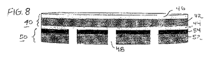
この種の製造は、レーザダイオードからの発光が、発光エリアに対して垂直に延びるので、面発光型半導体レーザアレイ(VCSELs)に非常に適している、つまり、その発光は、さいの目に切られた(または分割された)デバイスの表面に対して垂直に延びるので、ダイシングプロセスが、光の出るデバイス表面の光学的な質に影響することがない。しかし、端面発光レーザダイオードにとって、接合されたウェーハ構造を通るソーイングの機械的プロセスは、信号が通って出る光学面(すなわち、ファセット)の質に不利な影響を及ぼす可能性がある。この場合、図8−図10に関して以下に示されるステップ群を用いて、本発明に係る端面発光シングルエミッタレーザダイオード(および付随するサブマウント構造)のウェーハスケール製造を提供してもよい。 This kind of manufacture is very suitable for surface emitting semiconductor laser arrays (VCSELs), since the light emitted from the laser diode extends perpendicular to the light emitting area, ie, the light emission was diced. Since it extends perpendicular to the (or segmented) device surface, the dicing process does not affect the optical quality of the lighted device surface. However, for edge emitting laser diodes, the mechanical process of sawing through the bonded wafer structure can adversely affect the quality of the optical surface (ie, facet) through which the signal exits. In this case, the steps shown below with respect to FIGS. 8-10 may be used to provide wafer scale fabrication of the edge emitting single emitter laser diode (and associated submount structure) according to the present invention.
上記様々な実施形態と同様に、ウェーハ型レーザ配置80は、図8において、活性層84が形成される半導体ウェーハ82を具えるものとして示されている。このケースにおける面発光デバイスの光出力は、最終的に、活性層84からz−x面と平行な方向に出る。上部金属層86が、ウェーハ82の第1主要面に重なるように配置され、下部金属層88が、ウェーハ82の反対の第2主要面に重なるように配置されている。
Similar to the various embodiments described above, the wafer
図8に示されるように、ウェーハ型レーザ構造80は、サブマウントウェーハ90に取付けられ、特に、サブマウントウェーハ90の上部主要面に重なって形成された金属コンタクト層92に取付けられる。この実施形態の好ましい構成では、サブマウント90のCTEは、半導体ウェーハ82のCTEに比較的近い。レーザダイオード構造にサブマウントを最初に取付けるこのステップは、基本的に上記と同じである。
As shown in FIG. 8, the wafer
端面発光デバイスが使用されるこの形態においては、個別化プロセスを開始するにあたって、前述の実施形態のような、レーザ構造を通って「下に向かう」溝を形成する代わりに、サブマウントを通って「上に向かう」溝を形成することから開始することが提案される。この最初のステップは図9に示されており、複数の溝90が、サブマウントウェーハ90の下部表面90Bから上方に延びて形成される。上記溝50のように、端面発光デバイスの活性領域の既定の位置により、個々の溝90の配置および間隙を決定する。溝90の深さは、サブマウントウェーハ90、金属コンタクト層92、そしてときには、金属層86の一部も通るように選択される。半導体ウェーハ82に到達する前に止まるようトレンチプロセスを制御する。したがって、プロセスのこの時点では、端面発光放射のあるファセットの直接的なプロセスはない。
In this form, where an edge emitting device is used, instead of forming a “downward” groove through the laser structure as in the previous embodiment, the individualization process is initiated through the submount. It is suggested to start by forming an “upward” groove. This first step is illustrated in FIG. 9, in which a plurality of
図10に示されるように、プロセスの次のステップにて個々のレーザ発光領域を規定する。様々な周知技術を使用して、このステップを行う(例えば、下部金属層88を通るエッチング、ダイシング)。セパレーションは、図10において符号100で示されている。このプロセスにおいて、特に発光エリアで最高の滑らかな面とするには、結晶面に沿ってダイシングすることが好ましい。ダイシングは、大気中で行っても、真空中で行ってもよい。ダイシングに次いで、光学的に滑らかな面を作成するため、よく理解されているように、誘電材料および/または半導体材料でできた膜で、半導体デバイスの発光エリアを不動態化、またはコーティングする。
As shown in FIG. 10, individual laser emission areas are defined in the next step of the process. Various well-known techniques are used to perform this step (eg, etching through the
図11−12は、図9に示すプロセスの部分の代替例を示す。このケースにおいて、サブマウントウェーハ90と金属コンタクト層92の組合せは、最初に、金属コンタクト層92を通り、サブマウントウェーハ90の形成材料の中に延在する複数のグルーブ110を形成するよう加工される。図11に示されるように、グルーブ110は、サブマウントウェーハ90の厚みの一部のみを通って延在している。
FIGS. 11-12 show alternatives to the portions of the process shown in FIG. In this case, the combination of the
図11に示すように、グルーブが設けられたサブマウント構造に、レーザベースのウェーハ構造90を接合する。図12に示される以降のステップで、サブマウントウェーハ90の裏面を通る溝112が形成される。このケースにおいて、溝112の深さは、その前に形成したグルーブ110を曝露するだけの深さが必要である。このステップの完了後、図10に示す処理を用いて、最終的な間隔が密な形態を形成する。
As shown in FIG. 11, a laser-based
本発明の様々な好ましい実施形態を提供し、詳述してきたが、添付の請求項の範囲の意図または範囲を逸脱することなく、様々な変更および修正が可能であることを理解されたい。 While various preferred embodiments of the present invention have been provided and described in detail, it should be understood that various changes and modifications can be made without departing from the spirit or scope of the appended claims.
Claims (22)
ヒートシンク用材料の基板と、前記基板の上端に沿って間隔が密な構成に配置された複数の別々の金属領域と、を具えるサブマウントであって、前記別々のシングルエミッタレーザダイオードがそれぞれ、前記複数の別々の金属領域の上に個別に配置され接触していることを特徴とする光学システム。 An optical system comprising closely spaced light sources, comprising a plurality of separate single emitter laser diodes;
A submount comprising a substrate of heat sink material and a plurality of separate metal regions spaced closely along the top edge of the substrate, each of the separate single emitter laser diodes, An optical system, wherein the optical system is individually disposed and in contact with the plurality of separate metal regions.
a)レーザダイオードのアレイに関連する発光エリアのアレイを具える一体型レーザ構造を提供するステップと、
b)上部金属コンタクト層を具えるヒートシンクサブマウントを提供するステップと、
c)前記ヒートシンクサブマウントに前記一体型レーザ構造を取付けるステップと、
d)前記発光エリアの分離と前記複数の間隔の密なシングルエミッタレーザダイオードのため、ステップc)で作成した構成を個別化するステップと、
を具えることを特徴とする方法。 In a method of forming a plurality of closely spaced single emitter laser diodes supported by a single submount,
a) providing an integral laser structure comprising an array of light emitting areas associated with an array of laser diodes;
b) providing a heat sink submount comprising a top metal contact layer;
c) attaching the integrated laser structure to the heat sink submount;
d) individualizing the configuration created in step c) for the separation of the light emitting areas and the plurality of closely spaced single emitter laser diodes;
A method characterized by comprising.
d1)前記サブマウントおよび前記上部金属コンタクト層を通って上方に向かう複数の垂直な溝を形成するステップと、
d2)前記一体型レーザ構造を通してダイシングを行い、前記複数のレーザダイオードの前記複数の発光領域を画定するステップと、
を実施することを特徴とする方法。 In carrying out step d) in the method of claim 12,
d1) forming a plurality of vertical grooves upwardly through the submount and the upper metal contact layer;
d2) dicing through the integrated laser structure to define the plurality of light emitting regions of the plurality of laser diodes;
The method characterized by implementing.
Applications Claiming Priority (5)
| Application Number | Priority Date | Filing Date | Title |
|---|---|---|---|
| US201562117607P | 2015-02-18 | 2015-02-18 | |
| US62/117,607 | 2015-02-18 | ||
| US15/041,587 | 2016-02-11 | ||
| US15/041,587 US10186833B2 (en) | 2015-02-18 | 2016-02-11 | Densely-spaced laser diode configurations |
| PCT/US2016/018143 WO2016133943A1 (en) | 2015-02-18 | 2016-02-17 | Densely-spaced laser diode configurations |
Publications (1)
| Publication Number | Publication Date |
|---|---|
| JP2018508979A true JP2018508979A (en) | 2018-03-29 |
Family
ID=56622452
Family Applications (1)
| Application Number | Title | Priority Date | Filing Date |
|---|---|---|---|
| JP2017536027A Pending JP2018508979A (en) | 2015-02-18 | 2016-02-17 | Structure of closely spaced laser diodes |
Country Status (5)
| Country | Link |
|---|---|
| US (1) | US10186833B2 (en) |
| JP (1) | JP2018508979A (en) |
| CN (1) | CN107408791A (en) |
| DE (1) | DE112016000806T5 (en) |
| WO (1) | WO2016133943A1 (en) |
Families Citing this family (9)
| Publication number | Priority date | Publication date | Assignee | Title |
|---|---|---|---|---|
| US9728934B2 (en) * | 2015-08-31 | 2017-08-08 | Avago Technologies General Ip (Singapore) Pte. Ltd. | Back-side-emitting vertical cavity surface emitting laser (VCSEL) wafer bonded to a heat-dissipation wafer, devices and methods |
| JP6631502B2 (en) * | 2016-12-27 | 2020-01-15 | 日亜化学工業株式会社 | Laser package manufacturing method |
| WO2019023401A1 (en) * | 2017-07-25 | 2019-01-31 | Trilumina Corp. | A single-chip series connected vcsel array |
| US11482835B2 (en) | 2017-07-25 | 2022-10-25 | Lumentum Operations Llc | VCSEL device with multiple stacked active regions |
| WO2020026730A1 (en) * | 2018-07-30 | 2020-02-06 | パナソニック株式会社 | Semiconductor light emitting device and external resonance type laser device |
| JP7021618B2 (en) * | 2018-08-10 | 2022-02-17 | オムロン株式会社 | Manufacturing method of laser diode array device, laser emission circuit and ranging device |
| CN111211479A (en) * | 2018-11-21 | 2020-05-29 | 深圳市中光工业技术研究院 | Semiconductor laser chip and preparation method thereof |
| US20200395731A1 (en) * | 2019-06-11 | 2020-12-17 | Trumpf Photonics Inc. | Insulated Laser Coolers |
| CN115360583A (en) * | 2022-08-02 | 2022-11-18 | 佛山市国星光电股份有限公司 | Optical module |
Citations (10)
| Publication number | Priority date | Publication date | Assignee | Title |
|---|---|---|---|---|
| JPS5895889A (en) * | 1981-12-02 | 1983-06-07 | Mitsubishi Electric Corp | Semiconductor light emitting element array |
| JPH04286177A (en) * | 1991-03-14 | 1992-10-12 | Sumitomo Electric Ind Ltd | Submount for semiconductor laser |
| JPH09162496A (en) * | 1995-12-12 | 1997-06-20 | Nippon Telegr & Teleph Corp <Ntt> | Semiconductor laser and manufacturing method thereof |
| US20020172244A1 (en) * | 2001-05-17 | 2002-11-21 | Peng-Chih Li | Self-separating laser diode assembly and method |
| JP2003078199A (en) * | 2001-09-03 | 2003-03-14 | Fuji Photo Film Co Ltd | Semiconductor laser device |
| JP2006147874A (en) * | 2004-11-19 | 2006-06-08 | Fujitsu Ltd | Optical device and its manufacturing method |
| US20080025361A1 (en) * | 2006-07-19 | 2008-01-31 | Jerman John H | Linear diode-laser array with series-connected emitters |
| US20090190619A1 (en) * | 2008-01-30 | 2009-07-30 | Shenzhen Century Epitech Photonics Technology Co. Ltd. | Semiconductor laser package |
| JP2011249401A (en) * | 2010-05-24 | 2011-12-08 | Hamamatsu Photonics Kk | Method for manufacturing semiconductor laser |
| JP2015032706A (en) * | 2013-08-02 | 2015-02-16 | ウシオ電機株式会社 | Semiconductor device and manufacturing method thereof |
Family Cites Families (18)
| Publication number | Priority date | Publication date | Assignee | Title |
|---|---|---|---|---|
| US5848083A (en) | 1996-10-24 | 1998-12-08 | Sdl, Inc. | Expansion-matched high-thermal-conductivity stress-relieved mounting modules |
| DE19644941C1 (en) | 1996-10-29 | 1998-01-15 | Jenoptik Jena Gmbh | High power diode laser |
| US6178189B1 (en) | 1997-04-15 | 2001-01-23 | Opto Power Corporation | Multi-layer semiconductor devices with stress-relief profiles |
| TW393785B (en) * | 1997-09-19 | 2000-06-11 | Siemens Ag | Method to produce many semiconductor-bodies |
| US6995032B2 (en) * | 2002-07-19 | 2006-02-07 | Cree, Inc. | Trench cut light emitting diodes and methods of fabricating same |
| TWI227585B (en) * | 2002-12-13 | 2005-02-01 | Ind Tech Res Inst | Resonant cavity component array applicable on wavelength division multiplexing (WDM) and method for producing the same |
| KR20060039704A (en) * | 2004-11-03 | 2006-05-09 | 삼성전기주식회사 | Multi-wavelength laser diode and manufacturing method thereof |
| DE102005053274A1 (en) * | 2005-09-30 | 2007-04-12 | Osram Opto Semiconductors Gmbh | Making semiconductor chips involves building up semiconductor layers, applying metal plating to epitaxial growth substrate and depositing metal layer galvanically before structuring and separating layers into individual chips |
| US7864825B2 (en) | 2006-08-10 | 2011-01-04 | Lasertel, Inc. | Method and system for a laser diode bar array assembly |
| DE102007011564B4 (en) | 2007-03-07 | 2019-08-22 | Jenoptik Optical Systems Gmbh | Method for improved production of diode laser bars |
| US8320419B2 (en) * | 2007-09-20 | 2012-11-27 | Oclaro Technology Limited | High power semiconductor laser diodes |
| EP2191546B1 (en) * | 2007-09-20 | 2018-01-17 | II-VI Laser Enterprise GmbH | High power semiconductor laser diodes |
| US8068524B1 (en) | 2009-12-28 | 2011-11-29 | Pranalytica, Inc. | Submounts for Semiconductor Lasers |
| CN102074890B (en) * | 2010-12-14 | 2012-05-09 | 山东华光光电子有限公司 | Encapsulation method for die series laser |
| US9025635B2 (en) | 2011-01-24 | 2015-05-05 | Soraa Laser Diode, Inc. | Laser package having multiple emitters configured on a support member |
| US8518814B2 (en) | 2011-12-02 | 2013-08-27 | Northrop Grumman Systems Corporation | Methods of fabrication of high-density laser diode stacks |
| US8866041B2 (en) | 2012-04-12 | 2014-10-21 | Tdk Corporation | Apparatus and method of manufacturing laser diode unit utilizing submount bar |
| US9054063B2 (en) * | 2013-04-05 | 2015-06-09 | Infineon Technologies Ag | High power single-die semiconductor package |
-
2016
- 2016-02-11 US US15/041,587 patent/US10186833B2/en active Active
- 2016-02-17 CN CN201680010640.8A patent/CN107408791A/en active Pending
- 2016-02-17 JP JP2017536027A patent/JP2018508979A/en active Pending
- 2016-02-17 DE DE112016000806.6T patent/DE112016000806T5/en not_active Ceased
- 2016-02-17 WO PCT/US2016/018143 patent/WO2016133943A1/en not_active Ceased
Patent Citations (10)
| Publication number | Priority date | Publication date | Assignee | Title |
|---|---|---|---|---|
| JPS5895889A (en) * | 1981-12-02 | 1983-06-07 | Mitsubishi Electric Corp | Semiconductor light emitting element array |
| JPH04286177A (en) * | 1991-03-14 | 1992-10-12 | Sumitomo Electric Ind Ltd | Submount for semiconductor laser |
| JPH09162496A (en) * | 1995-12-12 | 1997-06-20 | Nippon Telegr & Teleph Corp <Ntt> | Semiconductor laser and manufacturing method thereof |
| US20020172244A1 (en) * | 2001-05-17 | 2002-11-21 | Peng-Chih Li | Self-separating laser diode assembly and method |
| JP2003078199A (en) * | 2001-09-03 | 2003-03-14 | Fuji Photo Film Co Ltd | Semiconductor laser device |
| JP2006147874A (en) * | 2004-11-19 | 2006-06-08 | Fujitsu Ltd | Optical device and its manufacturing method |
| US20080025361A1 (en) * | 2006-07-19 | 2008-01-31 | Jerman John H | Linear diode-laser array with series-connected emitters |
| US20090190619A1 (en) * | 2008-01-30 | 2009-07-30 | Shenzhen Century Epitech Photonics Technology Co. Ltd. | Semiconductor laser package |
| JP2011249401A (en) * | 2010-05-24 | 2011-12-08 | Hamamatsu Photonics Kk | Method for manufacturing semiconductor laser |
| JP2015032706A (en) * | 2013-08-02 | 2015-02-16 | ウシオ電機株式会社 | Semiconductor device and manufacturing method thereof |
Also Published As
| Publication number | Publication date |
|---|---|
| US10186833B2 (en) | 2019-01-22 |
| US20160240999A1 (en) | 2016-08-18 |
| DE112016000806T5 (en) | 2018-01-18 |
| WO2016133943A1 (en) | 2016-08-25 |
| CN107408791A (en) | 2017-11-28 |
| CN107408791A8 (en) | 2018-01-12 |
Similar Documents
| Publication | Publication Date | Title |
|---|---|---|
| JP2018508979A (en) | Structure of closely spaced laser diodes | |
| JP7165170B2 (en) | Manufacturing method and optoelectronic device | |
| US9172213B2 (en) | VCSEL module and manufacture thereof | |
| US7724791B2 (en) | Method of manufacturing laser diode packages and arrays | |
| JPH0629623A (en) | Monolithic laser diode array and its manufacture | |
| CN103843211A (en) | A method of assembling vcsel chips on a sub-mount | |
| EP3583667B1 (en) | Bonded laser with solder-free laser active stripe in facing relationship with submount | |
| JP2018511948A (en) | Monolithic semiconductor laser device | |
| JP2010226078A (en) | Light emitting device and manufacturing method thereof | |
| JP3386571B2 (en) | Method of manufacturing dual beam semiconductor laser | |
| CN105453350A (en) | Laser component and method for producing a laser component | |
| CN102856460B (en) | Light-emitting diode element, its manufacturing method, and light-emitting device | |
| US8153507B2 (en) | Method of manufacturing high power array type semiconductor laser device | |
| US5636235A (en) | Semiconductor laser device including columns of semiconductor lasers with non-central light emitting regions | |
| US9537286B2 (en) | Circuit system and manufacturing method for same | |
| US9450376B2 (en) | Method of producing a semiconductor laser element, and semiconductor laser element | |
| JP2019079906A (en) | Semiconductor laser array light source and optical fiber coupling module, and manufacturing method of semiconductor laser array light source | |
| JP2001208939A (en) | Optical element module, method of manufacturing laser chip with monitor, method of mounting laminated chip, method of manufacturing optical element module | |
| JP2007013002A (en) | Semiconductor laser equipment | |
| US9515453B2 (en) | Mounting layer for cooling structure | |
| JPH10242583A (en) | Semiconductor laser device manufacturing method and semiconductor laser device | |
| JP6037484B2 (en) | Manufacturing method of semiconductor laser device | |
| JP2019021801A (en) | Semiconductor light-emitting device array, and semiconductor light-emitting device | |
| JP2007073550A (en) | Semiconductor laser module and semiconductor laser stack |
Legal Events
| Date | Code | Title | Description |
|---|---|---|---|
| A521 | Request for written amendment filed |
Free format text: JAPANESE INTERMEDIATE CODE: A523 Effective date: 20171201 |
|
| A621 | Written request for application examination |
Free format text: JAPANESE INTERMEDIATE CODE: A621 Effective date: 20170919 |
|
| A977 | Report on retrieval |
Free format text: JAPANESE INTERMEDIATE CODE: A971007 Effective date: 20180829 |
|
| A131 | Notification of reasons for refusal |
Free format text: JAPANESE INTERMEDIATE CODE: A131 Effective date: 20180925 |
|
| A601 | Written request for extension of time |
Free format text: JAPANESE INTERMEDIATE CODE: A601 Effective date: 20181225 |
|
| A521 | Request for written amendment filed |
Free format text: JAPANESE INTERMEDIATE CODE: A523 Effective date: 20190222 |
|
| A131 | Notification of reasons for refusal |
Free format text: JAPANESE INTERMEDIATE CODE: A131 Effective date: 20190702 |
|
| A601 | Written request for extension of time |
Free format text: JAPANESE INTERMEDIATE CODE: A601 Effective date: 20191002 |
|
| A02 | Decision of refusal |
Free format text: JAPANESE INTERMEDIATE CODE: A02 Effective date: 20200218 |