JP2024018423A - semiconductor laser equipment - Google Patents
semiconductor laser equipment Download PDFInfo
- Publication number
- JP2024018423A JP2024018423A JP2022121765A JP2022121765A JP2024018423A JP 2024018423 A JP2024018423 A JP 2024018423A JP 2022121765 A JP2022121765 A JP 2022121765A JP 2022121765 A JP2022121765 A JP 2022121765A JP 2024018423 A JP2024018423 A JP 2024018423A
- Authority
- JP
- Japan
- Prior art keywords
- semiconductor laser
- recess
- mesa
- laser device
- axis direction
- Prior art date
- Legal status (The legal status is an assumption and is not a legal conclusion. Google has not performed a legal analysis and makes no representation as to the accuracy of the status listed.)
- Pending
Links
Images





Classifications
-
- H—ELECTRICITY
- H01—ELECTRIC ELEMENTS
- H01S—DEVICES USING THE PROCESS OF LIGHT AMPLIFICATION BY STIMULATED EMISSION OF RADIATION [LASER] TO AMPLIFY OR GENERATE LIGHT; DEVICES USING STIMULATED EMISSION OF ELECTROMAGNETIC RADIATION IN WAVE RANGES OTHER THAN OPTICAL
- H01S5/00—Semiconductor lasers
- H01S5/02—Structural details or components not essential to laser action
- H01S5/022—Mountings; Housings
- H01S5/023—Mount members, e.g. sub-mount members
-
- H—ELECTRICITY
- H01—ELECTRIC ELEMENTS
- H01S—DEVICES USING THE PROCESS OF LIGHT AMPLIFICATION BY STIMULATED EMISSION OF RADIATION [LASER] TO AMPLIFY OR GENERATE LIGHT; DEVICES USING STIMULATED EMISSION OF ELECTROMAGNETIC RADIATION IN WAVE RANGES OTHER THAN OPTICAL
- H01S5/00—Semiconductor lasers
- H01S5/02—Structural details or components not essential to laser action
- H01S5/022—Mountings; Housings
- H01S5/0233—Mounting configuration of laser chips
- H01S5/0234—Up-side down mountings, e.g. Flip-chip, epi-side down mountings or junction down mountings
-
- H—ELECTRICITY
- H01—ELECTRIC ELEMENTS
- H01S—DEVICES USING THE PROCESS OF LIGHT AMPLIFICATION BY STIMULATED EMISSION OF RADIATION [LASER] TO AMPLIFY OR GENERATE LIGHT; DEVICES USING STIMULATED EMISSION OF ELECTROMAGNETIC RADIATION IN WAVE RANGES OTHER THAN OPTICAL
- H01S5/00—Semiconductor lasers
- H01S5/02—Structural details or components not essential to laser action
- H01S5/022—Mountings; Housings
- H01S5/0235—Method for mounting laser chips
- H01S5/02375—Positioning of the laser chips
- H01S5/0238—Positioning of the laser chips using marks
-
- H—ELECTRICITY
- H01—ELECTRIC ELEMENTS
- H01S—DEVICES USING THE PROCESS OF LIGHT AMPLIFICATION BY STIMULATED EMISSION OF RADIATION [LASER] TO AMPLIFY OR GENERATE LIGHT; DEVICES USING STIMULATED EMISSION OF ELECTROMAGNETIC RADIATION IN WAVE RANGES OTHER THAN OPTICAL
- H01S5/00—Semiconductor lasers
- H01S5/20—Structure or shape of the semiconductor body to guide the optical wave ; Confining structures perpendicular to the optical axis, e.g. index or gain guiding, stripe geometry, broad area lasers, gain tailoring, transverse or lateral reflectors, special cladding structures, MQW barrier reflection layers
- H01S5/22—Structure or shape of the semiconductor body to guide the optical wave ; Confining structures perpendicular to the optical axis, e.g. index or gain guiding, stripe geometry, broad area lasers, gain tailoring, transverse or lateral reflectors, special cladding structures, MQW barrier reflection layers having a ridge or stripe structure
-
- H—ELECTRICITY
- H01—ELECTRIC ELEMENTS
- H01S—DEVICES USING THE PROCESS OF LIGHT AMPLIFICATION BY STIMULATED EMISSION OF RADIATION [LASER] TO AMPLIFY OR GENERATE LIGHT; DEVICES USING STIMULATED EMISSION OF ELECTROMAGNETIC RADIATION IN WAVE RANGES OTHER THAN OPTICAL
- H01S5/00—Semiconductor lasers
- H01S5/40—Arrangement of two or more semiconductor lasers, not provided for in groups H01S5/02 - H01S5/30
Landscapes
- Physics & Mathematics (AREA)
- Condensed Matter Physics & Semiconductors (AREA)
- General Physics & Mathematics (AREA)
- Electromagnetism (AREA)
- Optics & Photonics (AREA)
- Geometry (AREA)
- Semiconductor Lasers (AREA)
Abstract
Description
本開示は、半導体レーザ装置に関する。 The present disclosure relates to a semiconductor laser device.
従来、端面出射型の半導体レーザ素子が知られている。例えば特許文献1には、ジャンクションアップ方式によって、複数の発光点を有する半導体レーザ素子の表面(発光点を形成する活性層が設けられた側の面)とは反対側の裏面をマウント部材に実装する構成が開示されている。また、従来、ジャンクションアップ方式以外の実装方式として、半導体レーザ素子の表面をマウント部材に実装するジャンクションダウン方式も知られている。
2. Description of the Related Art Conventionally, edge-emitting semiconductor laser devices have been known. For example, in
しかしながら、上述したような従来の実装方式には、例えばリフロー半田付け等によって半田部材を介して半導体レーザ素子の表面又は裏面をマウント部材に実装する際に、半田部材の厚みが均一にならず、複数の発光点の高さ位置がばらつくという問題があった。 However, in the conventional mounting method as described above, when the front or back surface of the semiconductor laser element is mounted on the mount member via the solder member, for example, by reflow soldering, the thickness of the solder member is not uniform; There was a problem in that the height positions of the plurality of light emitting points varied.
また、発光点の数を増やした場合、半導体レーザ素子(基板)が複数の発光点の配列方向に横長の形状になることにより、半導体レーザ素子の反りが発生するおそれがある。 Furthermore, when the number of light emitting points is increased, the semiconductor laser element (substrate) becomes horizontally elongated in the direction in which the plurality of light emitting points are arranged, which may cause warpage of the semiconductor laser element.
そこで、本開示の一側面は、半導体レーザ素子の反りの発生を好適に抑制しつつ、複数の発光点の位置合わせを精度良く実行することができる半導体レーザ装置を提供することを目的とする。 Accordingly, one aspect of the present disclosure aims to provide a semiconductor laser device that can accurately align a plurality of light emitting points while suitably suppressing the occurrence of warpage of a semiconductor laser element.
本開示は、以下の[1]~[19]の半導体レーザ装置を含んでいる。 The present disclosure includes the following semiconductor laser devices [1] to [19].
[1]
第1方向において互いに反対側に位置する第1表面及び第2表面を有する基板と、第1方向に直交する第2方向に交差する光出射端面を有し、第2表面に形成された第1基準面に対して第1方向に突出すると共に第2方向に延在するように形成された複数のメサ部と、を有する半導体レーザ素子と、
第1基準面に対向する第2基準面を形成する第3表面と、第3表面に形成され、複数のメサ部が配置される複数の凹部と、を有するマウント部材と、
を備え、
メサ部は、凹部の底面に対向する頂面と、第1方向及び第2方向に直交する第3方向において互いに反対側に位置する一対の側面と、を有し、
メサ部の頂面には、メサ部と電気的に接続された第1電極が設けられており、
複数の凹部には、複数のメサ部の各々に対応する位置に配線部が設けられており、
複数のメサ部の各々に対応する第1電極は、半田部材を介して、配線部と電気的に接続されており、
第1基準面は、第2基準面と面接触しており、
互いに隣接する凹部間には、第2方向に延在すると共に第3方向に所定の長さを有し、第2基準面を有する隔壁部が設けられており、
凹部は、第3方向においてメサ部の側面に対向する第1側面を有し、
第2方向から見た場合に、第1側面と第1側面に対向するメサ部の側面との第3方向の距離は、第1方向に沿って頂面からメサ部の側面と第1基準面との境界である基端部に向かうにつれて短くなっている、
半導体レーザ装置。
[1]
A substrate having a first surface and a second surface located opposite to each other in a first direction, and a light emitting end surface that intersects in a second direction perpendicular to the first direction, and a first surface formed on the second surface. a semiconductor laser element having a plurality of mesa portions formed to protrude in a first direction with respect to a reference plane and extend in a second direction;
a mount member having a third surface forming a second reference surface opposite to the first reference surface; and a plurality of recesses formed on the third surface in which a plurality of mesa portions are disposed;
Equipped with
The mesa portion has a top surface facing the bottom surface of the recess, and a pair of side surfaces located on opposite sides in a third direction orthogonal to the first direction and the second direction,
A first electrode electrically connected to the mesa portion is provided on the top surface of the mesa portion,
Wiring portions are provided in the plurality of recesses at positions corresponding to each of the plurality of mesa portions,
The first electrode corresponding to each of the plurality of mesa portions is electrically connected to the wiring portion via a solder member,
The first reference surface is in surface contact with the second reference surface,
A partition wall portion extending in the second direction, having a predetermined length in the third direction, and having a second reference surface is provided between the mutually adjacent recessed portions,
The recess has a first side surface facing the side surface of the mesa portion in the third direction,
When viewed from the second direction, the distance in the third direction between the first side surface and the side surface of the mesa section opposite to the first side surface is the distance between the side surface of the mesa section and the first reference plane from the top surface along the first direction. It becomes shorter towards the proximal end, which is the boundary between the
Semiconductor laser equipment.
上記半導体レーザ装置では、半導体レーザ素子の第1基準面がマウント部材の第2基準面と面接触している。これにより、マウント部材の第2基準面に対する複数の発光点(例えば、光出射端面の第1方向における中心)の位置を精度良く揃えることができる。また、上記半導体レーザ装置では、互いに隣接する凹部間に設けられた隔壁部において第1基準面と第2基準面との接触面積を増やすことができるため、半導体レーザ素子(主に基板)にかかる応力を低減でき、半導体レーザ素子の反りの発生を抑制することができる。ここで、半導体レーザ素子の反りの発生を抑制する観点からは、第1基準面と第2基準面との接触面をなるべく大きくすることが好ましい。そのためには、凹部の第1側面及び第2基準面の境界部と当該第1側面に対向するメサ部の基端部との第3方向の距離をなるべく短くすることが好ましい。しかし、このように境界部と基端部との距離を短くした場合、凹部の第1側面とメサ部の側面(第1側面に対向する側面)とが接触し易くなり、メサ部が破損するリスクが高くなる。そこで、上記半導体レーザ装置では、凹部の第1側面とメサ部の側面との第3方向の距離が、第1方向に沿って頂面から基端部に向かうにつれて短くなるように構成されている。上記構成によれば、凹部の第1側面とメサ部の側面とが接触するリスクを低減しつつ、境界部と基端部との距離をなるべく短くすることができる。その結果、半導体レーザ素子の破損を抑制しつつ、第1基準面と第2基準面との接触面をなるべく大きくすることができる。従って、上記半導体レーザ装置によれば、半導体レーザ素子の反りの発生を好適に抑制しつつ、複数の発光点の位置合わせを精度良く実行することができる。 In the semiconductor laser device described above, the first reference surface of the semiconductor laser element is in surface contact with the second reference surface of the mount member. Thereby, the positions of the plurality of light emitting points (for example, the center of the light emitting end surface in the first direction) with respect to the second reference plane of the mount member can be aligned with high precision. In addition, in the semiconductor laser device described above, since the contact area between the first reference surface and the second reference surface can be increased in the partition section provided between the adjacent recesses, the contact area between the first reference surface and the second reference surface can be increased. Stress can be reduced and the occurrence of warpage of the semiconductor laser element can be suppressed. Here, from the viewpoint of suppressing the occurrence of warpage of the semiconductor laser element, it is preferable to make the contact surface between the first reference surface and the second reference surface as large as possible. To this end, it is preferable to make the distance in the third direction between the boundary between the first side surface of the recess and the second reference surface and the base end of the mesa section facing the first side surface as short as possible. However, when the distance between the boundary and the base end is shortened in this way, the first side of the recess and the side of the mesa (the side opposite to the first side) tend to come into contact, resulting in damage to the mesa. The risk is higher. Therefore, the semiconductor laser device is configured such that the distance in the third direction between the first side surface of the recess and the side surface of the mesa portion becomes shorter from the top surface toward the base end along the first direction. . According to the above configuration, the distance between the boundary portion and the base end portion can be made as short as possible while reducing the risk of contact between the first side surface of the recess and the side surface of the mesa portion. As a result, the contact surface between the first reference surface and the second reference surface can be made as large as possible while suppressing damage to the semiconductor laser element. Therefore, according to the semiconductor laser device described above, it is possible to suitably suppress the occurrence of warpage of the semiconductor laser element and to precisely align the plurality of light emitting points.
[2]
複数の凹部には、複数のメサ部の各々が個別に配置されている、
[1]の半導体レーザ装置。
上記構成によれば、各凹部間に設けられた複数の隔壁部において第1基準面と第2基準面との接触面積を増やすことができるため、半導体レーザ素子(主に基板)にかかる応力をより一層低減でき、半導体レーザ素子の反りの発生を効果的に抑制することができる。
[2]
Each of the plurality of mesa portions is individually arranged in the plurality of recesses,
[1] Semiconductor laser device.
According to the above configuration, it is possible to increase the contact area between the first reference surface and the second reference surface in the plurality of partitions provided between the respective recesses, thereby reducing the stress applied to the semiconductor laser element (mainly the substrate). This can be further reduced, and the occurrence of warpage in the semiconductor laser element can be effectively suppressed.
[3]
半導体レーザ素子は、それぞれ一以上のメサ部を含み、互いに独立して駆動可能に構成された複数のチャンネルを有する、
[1]又は[2]の半導体レーザ装置。
上記構成によれば、各チャンネル間で発光点の位置が高精度に揃えられたマルチチャンネル型の半導体レーザ装置を得ることができる。
[3]
The semiconductor laser device has a plurality of channels each including one or more mesa portions and configured to be able to be driven independently of each other.
The semiconductor laser device of [1] or [2].
According to the above configuration, it is possible to obtain a multi-channel semiconductor laser device in which the positions of the light emitting points are aligned with high precision between each channel.
[4]
配線部は、複数のメサ部の各々に対応する位置毎に配置され、互いに電気的に分離された複数の配線を含む、
[1]~[3]のいずれかの半導体レーザ装置。
上記構成によれば、互いに隣接する任意の2つのメサ部間を凹部間に設けられた隔壁部で分離することによって、各チャンネル間の短絡を防止しつつ、複数のメサ部を独立して駆動させることが可能となる。
[4]
The wiring part includes a plurality of wirings arranged at positions corresponding to each of the plurality of mesa parts and electrically isolated from each other.
The semiconductor laser device according to any one of [1] to [3].
According to the above configuration, by separating any two adjacent mesa portions by the partition wall provided between the recesses, a plurality of mesa portions can be driven independently while preventing short circuit between each channel. It becomes possible to do so.
[5]
第1表面には、複数のメサ部に共通の単一の第2電極が設けられている、
[1]~[4]のいずれかの半導体レーザ装置。
上記構成によれば、半導体レーザ素子の基板の裏面(第1表面)側に配置される電極部材(第2電極)を複数のメサ部間で共通化することにより、ワイヤボンディングによって当該電極部材に接続されるワイヤの本数を削減できるため、ワイヤボンディングによる半導体レーザ素子の損傷を抑制できる。
[5]
A single second electrode common to the plurality of mesa portions is provided on the first surface.
The semiconductor laser device according to any one of [1] to [4].
According to the above configuration, by making the electrode member (second electrode) arranged on the back surface (first surface) side of the substrate of the semiconductor laser element common among the plurality of mesa parts, the electrode member can be connected to the electrode member by wire bonding. Since the number of connected wires can be reduced, damage to the semiconductor laser element due to wire bonding can be suppressed.
[6]
凹部は、第3方向においてメサ部の側面に対向する第1側面を有し、
第1側面は、第3表面における凹部の第3方向に沿った開口幅が凹部の底面の第3方向に沿った幅よりも大きくなるように、底面に対して傾斜している、
[1]~[5]のいずれかの半導体レーザ装置。
上記構成によれば、凹部の第1側面を底面側から開口端側に向かって幅広となる傾斜面として構成することにより、凹部内において、リフロー時に溶けた半田部材を逃がすためのスペースを適切に確保することができる。
[6]
The recess has a first side surface facing the side surface of the mesa portion in the third direction,
The first side surface is inclined with respect to the bottom surface such that the opening width of the recess in the third surface along the third direction is larger than the width of the bottom surface of the recess along the third direction.
The semiconductor laser device according to any one of [1] to [5].
According to the above configuration, by configuring the first side surface of the recess as an inclined surface that becomes wider from the bottom side toward the opening end side, a space for escaping melted solder material during reflow can be appropriately created within the recess. can be secured.
[7]
第1基準面に対するメサ部の側面の傾斜角度は、底面に対する第1側面の傾斜角度よりも小さい、
[6]の半導体レーザ装置。
上記構成によれば、凹部の第1側面とメサ部の側面との第3方向の距離が凹部の頂面から基端部に向かうにつれて短くなる構成を、容易且つ確実に実現することができる。
[7]
The angle of inclination of the side surface of the mesa portion with respect to the first reference plane is smaller than the angle of inclination of the first side surface with respect to the bottom surface.
[6] Semiconductor laser device.
According to the above configuration, it is possible to easily and reliably realize a configuration in which the distance in the third direction between the first side surface of the recess and the side surface of the mesa portion becomes shorter from the top surface of the recess toward the base end.
[8]
第2基準面と凹部の第1側面とがなす角度は、鈍角である、
[1]~[7]のいずれかの半導体レーザ装置。
上記構成によれば、仮に半導体レーザ素子をマウント部材に実装する際に第2基準面と第1側面とが交わる部分にメサ部の側面が接触してしまったとしても、第2基準面と第1側面とがなす角度を90度以下に構成する場合と比較して、メサ部の側面に対する衝撃を低減できる。従って、上記構成によれば、実装時における半導体レーザ素子の破損のリスクを低減できる。
[8]
The angle between the second reference plane and the first side surface of the recess is an obtuse angle.
The semiconductor laser device according to any one of [1] to [7].
According to the above configuration, even if the side surface of the mesa portion comes into contact with the intersection of the second reference surface and the first side surface when mounting the semiconductor laser element on the mount member, the second reference surface and the first side surface may The impact on the side surface of the mesa portion can be reduced compared to the case where the angle formed by one side surface is 90 degrees or less. Therefore, according to the above configuration, the risk of damage to the semiconductor laser element during mounting can be reduced.
[9]
第2基準面と凹部の第1側面との境界部は、第3方向において、基端部から離間している、
[1]~[8]のいずれかの半導体レーザ装置。
上記構成によれば、境界部と基端部とが接触しないように半導体レーザ素子がマウント部材に実装されるため、実装時においてメサ部の側面が境界部に接触するリスクを低減し、半導体レーザ素子の破損を好適に防止することができる。
[9]
The boundary between the second reference plane and the first side surface of the recess is spaced apart from the base end in the third direction.
The semiconductor laser device according to any one of [1] to [8].
According to the above configuration, since the semiconductor laser element is mounted on the mount member so that the boundary part and the base end part do not come into contact with each other, the risk of the side surface of the mesa part coming into contact with the boundary part during mounting is reduced, and the semiconductor laser element Damage to the element can be suitably prevented.
[10]
配線部は、凹部の内部から凹部の外側の第3表面上まで延びている、
[1]~[9]のいずれかの半導体レーザ装置。
上記構成によれば、半導体レーザ素子のメサ部側の電極を第1電極及び配線部を介してマウント部材の表面(第3表面)まで引き出すことができるため、半導体レーザ素子に電流を流すための構成の実装が容易となる。
[10]
The wiring portion extends from the inside of the recess to the third surface outside the recess.
The semiconductor laser device according to any one of [1] to [9].
According to the above configuration, since the electrode on the mesa side of the semiconductor laser element can be drawn out to the surface (third surface) of the mount member via the first electrode and the wiring part, It is easier to implement the configuration.
[11]
配線部は、凹部の内部から凹部の外側まで第2方向に沿って延びており、
凹部は、第2方向に交差し、配線部が沿う第2側面を有し、
第2側面は、第3表面における凹部の第2方向に沿った開口幅が凹部の底面の第2方向に沿った幅よりも大きくなるように、底面に対して傾斜している、
[10]の半導体レーザ装置。
仮に第2側面が上記のように傾斜していない場合(例えば、第2側面が凹部の底面に対して垂直な面である場合)、配線部が段差状に折れ曲がってしまうため、断線が生じ易くなる。一方、上記のように第2側面を傾斜面として構成し、傾斜した第2側面に配線部を沿わせることにより、配線部が段差状に折れ曲がることを回避し、断線の発生を抑制することができる。
[11]
The wiring portion extends along the second direction from the inside of the recess to the outside of the recess,
The recess has a second side surface that intersects in the second direction and along which the wiring portion runs;
The second side surface is inclined with respect to the bottom surface such that the opening width of the recess in the third surface along the second direction is larger than the width of the bottom surface of the recess along the second direction.
The semiconductor laser device of [10].
If the second side surface is not sloped as described above (for example, if the second side surface is perpendicular to the bottom surface of the recess), the wiring part will be bent in a step shape, making it easy to break the wire. Become. On the other hand, by configuring the second side surface as an inclined surface as described above and placing the wiring section along the inclined second side surface, it is possible to avoid bending the wiring section into a stepped shape and suppress the occurrence of wire breakage. can.
[12]
複数のメサ部の各々は、メサ部毎に独立して設けられた一以上の活性層を有している、
[1]~[11]のいずれかの半導体レーザ装置。
上記構成によれば、複数のメサ部間において活性層が空間的に分離されるため、メサ部間の光学的クロストークの発生を確実に防止することができる。また、各メサ部に複数の活性層を設けた場合には、各メサ部をスタック型の半導体レーザ素子として機能させることができ、レーザ出力の増強を図ることができる。
[12]
Each of the plurality of mesa portions has one or more active layers provided independently for each mesa portion,
The semiconductor laser device according to any one of [1] to [11].
According to the above configuration, since the active layer is spatially separated between the plurality of mesa parts, it is possible to reliably prevent optical crosstalk between the mesa parts. Further, when each mesa portion is provided with a plurality of active layers, each mesa portion can function as a stacked semiconductor laser element, and the laser output can be increased.
[13]
マウント部材は、シリコンによって形成されている、
[1]~[12]のいずれかの半導体レーザ装置。
上記構成によれば、例えばエッチングプロセスによって、凹部を精度良く形成することができる。
[13]
The mount member is made of silicon.
The semiconductor laser device according to any one of [1] to [12].
According to the above configuration, the recess can be formed with high precision, for example, by an etching process.
[14]
マウント部材は、第3表面と接続され、第2方向に交差する第4表面を有し、
凹部は、第4表面まで延びており、第4表面に開口している、
[1]~[13]のいずれかの半導体レーザ装置。
上記構成によれば、凹部のうち第4表面に開口した部分から、凹部に配置された各メサ部の光出射端面を外部に露出させることができるため、光出射端面から第2方向に沿って出射される光の取り出し効率を向上させることができる。
[14]
The mount member has a fourth surface connected to the third surface and intersecting the second direction,
The recess extends to the fourth surface and is open to the fourth surface.
The semiconductor laser device according to any one of [1] to [13].
According to the above configuration, the light emitting end face of each mesa portion arranged in the recess can be exposed to the outside from the portion of the recess that is open to the fourth surface. The efficiency of extracting emitted light can be improved.
[15]
第3表面には、マウント部材に対して半導体レーザ素子を位置合わせするためのアライメントマークが設けられている、
[1]~[14]のいずれかの半導体レーザ装置。
上記構成によれば、マウント部材に半導体レーザ素子を実装する際に、マウント部材に対する半導体レーザ素子の位置合わせを容易且つ正確に行うことが可能となる。
[15]
The third surface is provided with an alignment mark for aligning the semiconductor laser element with respect to the mount member.
The semiconductor laser device according to any one of [1] to [14].
According to the above configuration, when mounting the semiconductor laser element on the mount member, it is possible to easily and accurately align the semiconductor laser element with respect to the mount member.
[16]
第2方向において半導体レーザ素子及びマウント部材と対向する位置に配置され、複数のメサ部の各々の光出射端面から出射される光を外部に向けて導光する光学素子と、
マウント部材及び光学素子を支持する支持基板と、
を更に備え、
支持基板は、マウント部材の第3表面とは反対側の第6表面と面接触してマウント部材を支持する第1支持面と、光学素子と面接触して光学素子を支持する第2支持面と、を有する、
[1]~[15]のいずれかの半導体レーザ装置。
上記構成によれば、半導体レーザ素子が搭載されたマウント部材と光学素子とが、支持基板の第1支持面及び第2支持面と面接触して支持されるため、半導体レーザ素子及び光学素子の高さ位置(すなわち、支持基板の支持面(第1支持面及び第2支持面)を基準とする各部材の高さ位置)を容易且つ精度良く合わせることができる。
[16]
an optical element that is disposed at a position facing the semiconductor laser element and the mount member in a second direction and guides light emitted from the light emitting end face of each of the plurality of mesa parts toward the outside;
a support substrate that supports the mount member and the optical element;
further comprising;
The support substrate includes a first support surface that supports the mount member in surface contact with a sixth surface opposite to the third surface of the mount member, and a second support surface that supports the optical element in surface contact with the optical element. and has
The semiconductor laser device according to any one of [1] to [15].
According to the above configuration, the mount member on which the semiconductor laser element is mounted and the optical element are supported in surface contact with the first support surface and the second support surface of the support substrate. The height positions (that is, the height positions of each member with respect to the support surface (first support surface and second support surface) of the support substrate) can be easily and accurately matched.
[17]
光学素子は、複数のメサ部の各々の光出射端面から出射される光が入射される光入射面を有し、
マウント部材は、光入射面に対向する第4表面を有し、
光入射面は、第4表面と面接触している、
[16]の半導体レーザ装置。
上記構成によれば、第2方向において互いに対向するマウント部材の第4表面と光学素子の光入射面とを面接触させることにより、第2方向における光出射端面と光入射面との距離を精度良く調整することができる。すなわち、マウント部材に半導体レーザ素子を実装する際に、第2方向における光出射端面から第4表面までの距離を調整することにより、光出射端面から光入射面までの距離を調整することができる。
[17]
The optical element has a light incident surface into which light emitted from each of the plurality of mesa portions is incident,
The mount member has a fourth surface facing the light incident surface,
The light incident surface is in surface contact with the fourth surface.
The semiconductor laser device of [16].
According to the above configuration, by bringing the fourth surface of the mount member facing each other in the second direction into surface contact with the light incident surface of the optical element, the distance between the light output end surface and the light incident surface in the second direction can be accurately adjusted. Can be adjusted well. That is, when mounting the semiconductor laser element on the mount member, by adjusting the distance from the light emitting end surface to the fourth surface in the second direction, the distance from the light emitting end surface to the light incident surface can be adjusted. .
[18]
凹部の第2方向の長さは、半導体レーザ素子の第2方向の長さよりも長い、
[1]~[17]のいずれかの半導体レーザ装置。
上記構成によれば、凹部のうち第2方向において半導体レーザ素子(メサ部)と重ならない空間に、リフロー時に溶けた半田部材を逃すことが可能となる。また、光学素子がレンズである場合等において、レンズの焦点距離に応じて、マウント部材に対する半導体レーザ素子の第2方向の位置を調整することが可能となる。
[18]
The length of the recess in the second direction is longer than the length of the semiconductor laser element in the second direction.
The semiconductor laser device according to any one of [1] to [17].
According to the above configuration, it is possible to release the solder material melted during reflow into a space in the recess that does not overlap with the semiconductor laser element (mesa part) in the second direction. Furthermore, when the optical element is a lens, the position of the semiconductor laser element in the second direction relative to the mount member can be adjusted depending on the focal length of the lens.
[19]
支持基板上において、光学素子、マウント部材、及び半導体レーザ素子を覆うように形成されたモールド樹脂を更に備える、
[15]~[18]のいずれかの半導体レーザ装置。
上記構成によれば、モールド樹脂によって、支持基板上に配置された各部材(光学素子、マウント部材、及び半導体レーザ素子)の位置関係を固定することができるため、各部材の位置関係のずれが発生することを防止できる。また、モールド樹脂によって各部材を適切に保護することができる。
[19]
Further comprising a mold resin formed to cover the optical element, the mounting member, and the semiconductor laser element on the support substrate.
The semiconductor laser device according to any one of [15] to [18].
According to the above configuration, the positional relationship of each member (optical element, mount member, and semiconductor laser element) arranged on the support substrate can be fixed by the molded resin, so that deviations in the positional relationship of each member can be prevented. This can be prevented from occurring. Moreover, each member can be appropriately protected by the mold resin.
本開示の一側面によれば、半導体レーザ素子の反りの発生を好適に抑制しつつ、複数の発光点の位置合わせを精度良く実行することができる半導体レーザ装置を提供することができる。 According to one aspect of the present disclosure, it is possible to provide a semiconductor laser device that can accurately align a plurality of light emitting points while suitably suppressing the occurrence of warpage of a semiconductor laser element.
以下、本開示の一実施形態について、図面を参照しつつ詳細に説明する。なお、以下の説明において、同一又は相当要素には同一符号を用い、重複する説明を省略する。 Hereinafter, one embodiment of the present disclosure will be described in detail with reference to the drawings. In the following description, the same or equivalent elements will be denoted by the same reference numerals, and overlapping description will be omitted.
[第1実施形態]
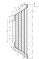
図1~図9を参照して、第1実施形態の半導体レーザ装置1Aについて説明する。図1に示されるように、半導体レーザ装置1Aは、半導体レーザ素子10と、サブマウント20(マウント部材)と、を備えている。半導体レーザ素子10は、ジャンクションダウン方式によって、サブマウント20上に実装されている。すなわち、半導体レーザ素子10は、活性層13(図3参照)が設けられた側の表面(下面11b)がサブマウント20に対向するようにして、サブマウント20上に搭載されている。
[First embodiment]
A
本実施形態では、サブマウント20に対して半導体レーザ素子10が搭載される側を上側とし、半導体レーザ素子10から外部に向けたレーザ光Lが出射される側を前側とする。また、上記定義を前提として、上下方向をZ軸方向(第1方向)と表し、前後方向をY軸方向(第2方向)と表し、左右方向をX軸方向(第3方向)と表す。Z軸方向は、半導体レーザ素子10とサブマウント20とが対向する方向と一致する。Y軸方向は、Z軸方向に直交する方向であり、半導体レーザ素子10が有する複数のメサ部12の各々が延在する方向(すなわち、レーザ出射方向)と一致する。X軸方向は、Z軸方向及びY軸方向の両方に直交する方向であり、複数のメサ部12の配列方向と一致する。
In this embodiment, the side on which the
半導体レーザ素子10は、端面出射型の半導体レーザ素子である。半導体レーザ素子10は、基板11と、複数(本実施形態では8つ)のメサ部12と、を有している。半導体レーザ素子10は、単一のチャンネルのみを有するシングルチャンネル型であってもよいし、複数のチャンネルを有するマルチチャンネル型であってもよい。ここで、「チャンネル」とは、同時に発光する単位である。言い換えれば、チャンネルは、独立して駆動可能な単位である。一つのチャンネルは、一以上のメサ部12によって構成される。例えば、2以上のメサ部12が電気的に接続されている場合には、当該2以上のメサ部12によって1つのチャンネルが構成される。本実施形態では、一例として、複数のメサ部12の各々が互いに電気的に分離されているため、メサ部12とチャンネルとは「1:1」の関係を有している。すなわち、本実施形態では、半導体レーザ素子10は、マルチチャンネル(8チャンネル)型の半導体レーザ素子として構成されており、メサ部12の数(8つ)とチャンネル数とが一致している。
The
基板11は、例えば化合物半導体基板等の半導体基板である。基板11は、矩形板状(直方体状)に形成されている。図1及び図2に示されるように、基板11は、Z軸方向において互いに反対側に位置する上面11a(第1表面)及び下面11b(第2表面)と、Y軸方向において互いに反対側に位置する前面11c及び後面11dと、X軸方向において互いに反対側に位置する側面11e,11f(第5表面)と、を有している。
The
基板11の上面11aには、カソード電極である電極32(第2電極)が設けられている。一例として、電極32は、複数のメサ部12に共通の単一の電極として構成されている。すなわち、電極32は、Z軸方向において複数のメサ部12と重なるように、上面11aの略全面に設けられている。電極32は、例えば、AuGe、Ni、Au等の金属材料によって形成され得る。電極32の上面には、ワイヤボンディング等によって、図示しない電源回路と電気的に接続するためのワイヤが接続され得る。
An electrode 32 (second electrode), which is a cathode electrode, is provided on the
複数のメサ部12は、それぞれ独立してレーザ光Lを出射する光出射端面12aを有している。図2に示されるように、複数(本実施形態では8つ)のメサ部12は、X軸方向に沿って略等間隔に配列されている。各メサ部12の光出射端面12aは、Y軸方向に交差しており、Y軸方向に沿ってレーザ光Lを出射する。なお、光出射端面12aは、各メサ部12のY軸方向の両側(前側及び後側)に設けられているが、本実施形態では、前側の光出射端面12aが、外部に向けてレーザ光Lを出射する光出射端面として機能する。従って、後側の光出射端面12aには、後方に向けてレーザ光Lが出射されないようにするために、反射膜等が設けられてもよい。一方、前側の光出射端面12aには、外部への光の取り出し効率を高めるために、低反射膜が設けられてもよい。
The plurality of
図2に示されるように、各メサ部12は、基板11の下面11bに形成された基準面R1(第1基準面)に対してZ軸方向に突出するように形成されている。また、各メサ部12は、Y軸方向に延在するように形成されている。基準面R1は、サブマウント20の基準面R2(第2基準面)に面接触することによりサブマウント20に直接支持される面である。一例として、下面11bの全体(メサ部12の表面を含む)に、絶縁層19が所定の厚みで連続的に形成される。この場合、絶縁層19の基板11に対向する側とは反対側の表面19aが、基準面R1として機能する。
As shown in FIG. 2, each
各メサ部12は、頂面12bと、一対の側面12cと、を有している。頂面12bは、サブマウント20の凹部21(図4参照)に対向する面である。言い換えれば、頂面12bは、メサ部12に対して基板11が位置する側とは反対側を向く面である。一例として、頂面12bは、絶縁層19の表面19aのうち、後述するコンタクト層18の表面18aを覆う部分によって形成される。一対の側面12cは、X軸方向において互いに反対側に位置する面である。側面12cは、頂面12bと基準面R1とを接続する面である。一対の側面12cは、X軸方向における一対の側面12c同士の間隔が頂面12bから基準面R1に向かうにつれて幅広となるように、頂面12b及び基準面R1に対して傾斜している。すなわち、各メサ部12は、Y軸方向から見た場合に、台形状に形成されている。
Each
各メサ部12の頂面12bには、各メサ部12と電気的に接続されるアノード電極である電極35(第1電極)が設けられている。すなわち、電極35は、メサ部12毎に設けられている。電極35は、例えば、Ti、Pt、Au等の金属材料によって形成され得る。図2に示されるように、一例として、電極35は、メサ部12の頂面12bの大部分(頂面12bのY軸方向における両側縁部を除いた部分)を覆うと共に、Y軸方向に延在するように設けられている。
An electrode 35 (first electrode) that is an anode electrode electrically connected to each
図3に示されるように、メサ部12は、基板11の下面11b上に形成された積層構造を有している。一例として、メサ部12は、4つの第1積層構造体L1と、3つの第2積層構造体L2と、コンタクト層18と、を含んでいる。より具体的には、基板11の下面11b上に最下部(最も基板11に近い側)の第1積層構造体L1が積層されている。その上に、1つの第2積層構造体L2が2つの第1積層構造体L1に挟まれる繰り返し構造が形成されるように、3つの第1積層構造体L1と3つの第2積層構造体L2とが積層されている。最上部(最も基板11から遠い側)の第1積層構造体L1上には、コンタクト層18が積層されている。
As shown in FIG. 3, the
第1積層構造体L1は、活性層13と、第1半導体層14と、第2半導体層15と、を含んでいる。第1積層構造体L1を構成する各層は、下面11b側から、第1半導体層14、活性層13、第2半導体層15の順に積層されている。活性層13は、例えば、量子井戸層と障壁層とがZ軸方向に交互に積層された量子井戸構造を含む層であり、レーザ光Lを発生させる層である。活性層13は、例えば、InGaAs層とInAlAs層とを積層方向(Z軸方向)に沿って交互に複数積層した構造を有している。第1半導体層14は、例えば、n型のAlGaAs層によって形成され得る。第2半導体層15は、例えば、p型のAlGaAs層によって形成され得る。
The first stacked structure L1 includes an
第2積層構造体L2は、いわゆるトンネルジャンクションであり、第1トンネル接合層16と、第2トンネル接合層17と、を含んでいる。第1トンネル接合層16は、第2トンネル接合層17よりも下面11b側に位置している。第1トンネル接合層16は、例えば、p型ドーパントの高濃度ドープGaAs層によって形成され得る。第2トンネル接合層17は、例えば、n型ドーパントの高濃度ドープGaAs層によって形成され得る。
The second stacked structure L2 is a so-called tunnel junction, and includes a first
コンタクト層18は、例えば、p型ドーパントの高濃度ドープGaAs層によって形成され得る。コンタクト層18は、上述した電極35と接触する層である。コンタクト層18の基板11に対向する側とは反対側の表面18aを覆う絶縁層19には、表面18aの少なくとも一部を露出させるための開口部19bが設けられている。図2及び図3に示されるように、開口部19bは、電極35とコンタクト層18とが重なる部分において、X軸方向における頂面12bの中央部に設けられている。Z軸方向から見た場合に、開口部19bは、Y軸方向に延在する長方形状に形成されている。本実施形態では、図2において電極35が窪んだ部分が、開口部19bが形成された部分に対応する。開口部19bにおいて、電極35がコンタクト層18側へと入り込むことによって、電極35の表面が窪んでいる。コンタクト層18の表面18aのうちZ軸方向において開口部19bと重なる領域(すなわち、外部に露出した領域)が、電極35と接触するコンタクト領域CAとして機能する。本実施形態では、絶縁層19がコンタクト層18の表面18aのX軸方向の両側縁部を覆っているため、コンタクト領域CAのX軸方向の長さd1は、頂面12bのX軸方向の長さよりも短くなっている。
The
サブマウント20は、例えば、シリコンによって形成されたシリコン基板である。サブマウント20の内部には、半導体レーザ素子10を駆動させるための回路が内蔵されてもよい。図4に示されるように、サブマウント20は、矩形板状(直方体状)に形成されている。サブマウント20は、Z軸方向において互いに反対側に位置する上面20a(第3表面)及び下面20b(第6表面)と、Y軸方向において互いに反対側に位置する前面20c(第4表面)及び後面20dと、X軸方向において互いに反対側に位置する側面20e,20fと、を有している。上面20aは、半導体レーザ素子10の基準面R1に対向する面であり、基準面R1と面接触する基準面R2を形成する。本実施形態では、半導体レーザ素子10の基準面R1が、基板11の下面11bに設けられた絶縁層19の表面19aによって形成されているのに対して、サブマウント20の基準面R2は、サブマウント20自体の表面(上面20a)によって形成されている。
The
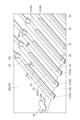
サブマウント20は、上面20aに形成された凹部21を有している。凹部21は、半導体レーザ素子10に設けられた複数のメサ部12を配置(収容)するために、上面20aの他の部分よりも下面20b側に窪むように形成された部分である。凹部21は、例えばウェットエッチングによって形成され得る。一例として、凹部21は、複数のメサ部12の各々を個別に収容する複数(本実施形態では8つ)の凹部22によって構成されている。すなわち、本実施形態では、上面20aに、複数のメサ部12の各々に対応するようにX軸方向に配列された複数の凹部22が設けられている。各凹部22のY軸方向の長さは、基板11のY軸方向の長さよりも長くされている。互いに隣接する凹部22間には、隔壁部23が設けられている。隔壁部23は、Y軸方向に延在すると共にX軸方向に所定の長さ(すなわち、一定以上の幅)を有し、基準面R2を有している。すなわち、隣接する凹部22同士は、X軸方向に一定以上の間隔を空けて配置されており、この間隔に対応する部分(すなわち、凹部22が形成されていない部分)が、隔壁部23として機能する。
The
図4、図5及び図6に示されるように、凹部22は、Y軸方向に延在する溝状に形成されている。凹部22は、前面20cまで延びており、前面20cに開口している。凹部22は、Z軸方向に交差する底面22aと、X軸方向に交差する一対の側面22b(第1側面)と、Y軸方向に交差する側面22c(第2側面)と、を有している。なお、図4、図5及び図6は、サブマウント20に半導体レーザ素子10が実装される前の状態を示している。
As shown in FIGS. 4, 5, and 6, the
一対の側面22bは、半導体レーザ素子10がサブマウント20に実装された実装状態において、X軸方向においてメサ部12の側面12cと対向する面である。側面22bは、上面20aにおける凹部22のX軸方向に沿った開口幅が凹部22の底面22aのX軸方向に沿った幅よりも大きくなるように、底面22aに対して傾斜している。すなわち、図6の(A)に示されるように、底面22aに対する側面22bの傾斜角度θ1は、鋭角をなしている。一方、上面20a(基準面R2)と側面22bとがなす角度θ2は、鈍角である。一例として、凹部22がウェットエッチングによって形成されることによって、側面22bは、平面状に形成されている。この場合、傾斜角度θ1と角度θ2とは、「θ1+θ2=180°」の関係を有している。
The pair of side surfaces 22b are surfaces that face the side surfaces 12c of the
側面22cは、凹部22の後方に形成された面である。側面22cは、上面20aにおける凹部22のY軸方向に沿った開口幅が凹部22の底面22aのY軸方向に沿った幅よりも大きくなるように、底面22aに対して傾斜している。すなわち、図6の(B)に示されるように、底面22aに対する側面22cの傾斜角度θ3は、鋭角をなしている。一例として、凹部22がウェットエッチングによって形成されることによって、傾斜角度θ3は、傾斜角度θ1と略一致している。
The
凹部21には、複数のメサ部12の各々に対応する位置に配線部Wが設けられている。一例として、配線部Wは、複数のメサ部12の各々に対応する位置毎に配置された複数の配線31を含んでいる。配線31は、例えばAu等の金属材料によって形成され得る。本実施形態では、メサ部12毎に独立した凹部22が形成されているため、図5に示されるように、凹部22毎に個別の配線31が設けられている。各凹部22において、配線31は、底面22aに沿ってY軸方向に延びている。図4及び図5に示されるように、配線31は、凹部22の内部から凹部22の外側の上面20a上まで延びている。一例として、各配線31は、上面20a上にそれぞれ独立して設けられた電極パッド34まで延びている。すなわち、複数の配線31は、互いに電気的に分離されている。これにより、複数のメサ部12の各々に対して独立して電流を流すこと(すなわち、各メサ部12を独立して駆動させること)が可能となっている。図5及び図6の(B)に示されるように、配線31は、底面22a及び側面22cに沿っている。すなわち、側面22cは、配線31を凹部22の内部から凹部22の外側へと誘導する役割を果たしている。なお、各電極パッド34には、ワイヤボンディング等によって、図示しない電源回路と電気的に接続するためのワイヤが接続され得る。
A wiring portion W is provided in the
図5及び図6の(A)に示されるように、各凹部22内において、配線31上には、半田部材33が蒸着等によって設けられている。半田部材33は、例えばSn、Ag、Cu等のリフロー半田付けに適した材料によって形成され得る。
As shown in FIGS. 5 and 6A, a
図7を参照して、サブマウント20に対する半導体レーザ素子10の実装工程について説明する。まず、図7のS1に示されるように、各凹部22内の配線31上に半田部材33が配置される。続いて、図7のS2に示されるように、半導体レーザ素子10の各メサ部12の位置と凹部22の位置とを合わせると共に、基準面R1が基準面R2に対向するようにして半導体レーザ素子10をサブマウント20上に載置する。すなわち、各メサ部12の頂面12bに設けられた電極35を、各凹部22に配置された半田部材33の上面と接触させる。続いて、図7のS2に示される状態の半導体レーザ素子10及びサブマウント20をリフロー炉で加熱することにより、半田部材33が溶融し、半導体レーザ素子10がサブマウント20に吸着される。具体的には、半田部材33が溶融して半田部材33のZ軸方向の厚みが減少することにより、半導体レーザ素子10の基準面R1とサブマウント20の基準面R2とが接触するまで、半導体レーザ素子10がサブマウント20側へと移動する。その結果、図7のS3に示されるように、複数のメサ部12の各々が凹部22内に収容されると共に、基準面R1と基準面R2とが面接触した状態となる。また、複数のメサ部12の各々に対応する電極35が、半田部材33を介して、対応する配線31と電気的に接続された状態となる。
Referring to FIG. 7, the process of mounting the
図8に示されるように、サブマウント20の上面20aには、図7に示した実装工程においてサブマウント20に対して半導体レーザ素子10を位置合わせするためのアライメントマークMが設けられている。一例として、アライメントマークMは、平面視において十字形状を有している。アライメントマークMは、実装状態における半導体レーザ素子10のX軸方向の両側に配置されている。図8に示されるように、各アライメントマークMのX軸方向における内側端部を側面11e,11fに沿わせることにより、サブマウント20に対する半導体レーザ素子10のX軸方向の位置合わせを行うことが可能となっている。また、一例として、電極32のX軸方向における両側端部には、アライメントマークMに対応する目印(凹部32a)が設けられている。アライメントマークMのうちX軸方向の内側に延びる部分M1が凹部32aとY軸方向において重なるように位置合わせを行うことにより、サブマウント20に対する半導体レーザ素子10のY軸方向の位置合わせを行うことが可能となっている。なお、本実施形態では、このような位置合わせにより、半導体レーザ素子10の前面11cとサブマウント20の前面20cとが略面一となるように、半導体レーザ素子10がサブマウント20に対して配置されるため、前面11cと前面20cとを合わせることによっても、サブマウント20に対する半導体レーザ素子10のY軸方向の位置を決定することができる。ただし、例えば、基板11の前面11cがサブマウント20の前面20cよりも前方又は後方に位置するように半導体レーザ素子10が配置される場合には、上述した部分M1及び凹部32aを目印として用いることにより、半導体レーザ素子10のY軸方向の位置を適切に決定することができる。
As shown in FIG. 8, an alignment mark M is provided on the
図9を参照して、実装状態における各メサ部12の位置関係について説明する。図9は、複数(本実施形態では8つ)のメサ部12のうち互いにX軸方向に隣接する2つのメサ部12を含む部分をY軸方向(前方)から見た側面図である。ここでは、2つのメサ部12のうち前方から見て左側のメサ部12を第1メサ部12Aとし、右側のメサ部12を第2メサ部12Bとする。
With reference to FIG. 9, the positional relationship of each
第1メサ部12Aが収容された凹部22に配置された配線31である第1配線31Aは、第2メサ部12Bが収容された凹部22に配置された配線31である第2配線31Bと電気的に分離(絶縁)されている。言い換えれば、複数の配線31は、X軸方向に互いに隣接して配置され且つ互いに電気的に分離された第1配線31A及び第2配線31Bを含んでいる。また、第1配線31Aと電気的に接続された半田部材33が第2配線31Bと電気的に接続された半田部材33と接触しないように配置されていることにより、第1配線31Aと電気的に接続された第1メサ部12Aは、第2配線31Bと電気的に接続された第2メサ部12Bと電気的に分離されている。なお、本実施形態では、上述した通り、複数の配線31は、互いに電気的に分離されている。従って、複数の配線31のうちX軸方向に互いに隣接して配置された任意の2つの配線31が、第1配線31A及び第2配線31Bに該当する。
The
ここで、メサ部12の側面12cと基準面R1との境界を基端部Pと表し、第1メサ部12Aに対して第2メサ部12Bが位置する側の第1メサ部12Aの側面12cと基準面R1との境界である基端部Pを第1基端部P1と表し、第2メサ部12Bに対して第1メサ部12Aが位置する側の第2メサ部12Bの側面12cと基準面R1との境界である基端部Pを第2基端部P2と表す。このとき、第1基端部P1から第2基端部P2までのX軸方向の距離d2は、メサ部12のコンタクト領域CAのX軸方向の長さd1よりも長い。
Here, the boundary between the
また、Y軸方向から見た場合に、凹部22の側面22bと当該側面22bに対向するメサ部12の側面12cとのX軸方向の距離d4は、Z軸方向に沿って頂面12bからメサ部12の側面12cと基準面R1との境界である基端部Pに向かうにつれて短くなっている。
Further, when viewed from the Y-axis direction, the distance d4 in the X-axis direction between the
[作用効果]
以下、上述した半導体レーザ装置1Aの作用効果について説明する。
[Effect]
Hereinafter, the effects of the
(第1の作用効果)
半導体レーザ装置1Aでは、半導体レーザ素子10の基準面R1(本実施形態では、絶縁層19の表面19a)がサブマウント20の基準面R2と面接触している。これにより、サブマウント20の基準面R2に対する複数の発光点(例えば、光出射端面12aのZ軸方向における中心)の位置を精度良く揃えることができる。また、半導体レーザ装置1Aは、互いに電気的に分離される(すなわち、互いに独立して駆動可能に構成される)と共に互いに隣接して配置された第1メサ部12A及び第2メサ部12Bを有する。ここで、コンタクト領域CAの幅(X軸方向の長さd1)によって、必要となる半田部材33の量(例えば、X軸方向における半田部材33の幅)が変化し得るが、半導体レーザ装置1Aでは、第1メサ部12Aと第2メサ部12Bとの間隔(すなわち、X軸方向における第1基端部P1から第2基端部P2までの距離d2)がコンタクト領域CAの長さd1よりも長くされている。これにより、コンタクト領域CAの長さd1に応じて必要となる半田部材33の量に対して、第1メサ部12Aと第2メサ部12Bとの間隔を十分に確保することができる。その結果、リフロー半田付けによって半導体レーザ素子10をサブマウント20に実装する際に、第1メサ部12Aに対応する半田部材33と第2メサ部12Bに対応する半田部材33とが溶けて互いに接触してしまうことを好適に防止できる。従って、半導体レーザ装置1Aによれば、互いに独立して駆動可能に構成されたチャンネル間の短絡を防止しつつ、複数の発光点の位置合わせを精度良く実行することができる。
(First effect)
In the
さらに、半導体レーザ装置1Aは、上記第1の作用効果に関連して、以下の構成を備えている。すなわち、図9に示されるように、凹部21は、第1メサ部12Aが収容(配置)される凹部22である第1凹部22Aと、第2メサ部12Bが収容される凹部22である第2凹部22Bと、を有している。また、第1凹部22Aと第2凹部22Bとの間に形成された隔壁部23(すなわち、第1凹部22Aと第2凹部22Bとを分離するようにY軸方向に延在する部分)の基準面R2のX軸方向の長さd3は、コンタクト領域CAのX軸方向の長さd1よりも長い。図9に示されるように、本実施形態では、基準面R2と凹部22の側面22bとの境界部Bは、X軸方向において、基端部Pから離間している。このため、「d2>d3>d1」の関係が成立している。なお、長さd3は、基準面R2及び第1凹部22Aの境界部B(第2凹部22B側の境界部B)と基準面R2及び第2凹部22Bの境界部B(第1凹部22A側の境界部B)とのX軸方向の長さである。上記構成によれば、第1メサ部12Aと第2メサ部12Bとを互いに異なる凹部22(第1凹部22A及び第2凹部22B)に収容すると共に第1凹部22Aと第2凹部22Bとの間の隔壁部23の幅(長さd3)を十分に確保することにより、リフロー時に溶けた第1メサ部12A(又は第2メサ部12B)に対応する半田部材33が隔壁部23を越えて第2メサ部12B(又は第1メサ部12A)に対応する半田部材33と接触(短絡)することを好適に防止できる。
Furthermore, the
また、凹部21は、複数のメサ部12の各々が個別に収容される複数の凹部22によって構成されており、互いに隣接する凹部22間に隔壁部23が設けられている。上記構成によれば、2以上のメサ部12が収容される単一の凹部22を含む構成と比較して、隣接するメサ部12間の短絡を好適に防止できると共に、複数のチャンネルの独立駆動の信頼性を向上させることができる。さらに、各凹部22間に設けられた隔壁部23において基準面R1と基準面R2との接触面積を増やすことができるため、半導体レーザ素子10(主に基板11)にかかる応力を低減でき、半導体レーザ素子10の反りの発生を抑制することができる。特に、本実施形態のようにX軸方向に複数のメサ部12が配列されることによって基板11のX軸方向の長さが長くなると、X軸方向に対して基板11の反りが発生し易くなる。上記構成は、このような場合に特に有効である。
Further, the
なお、本実施形態では、第1メサ部12Aと第2メサ部12Bとが別々の凹部22に収容されることによって、第1メサ部12Aに対応する半田部材33と第2メサ部12Bに対応する半田部材33とが互いに接触することが効果的に防止されるが、上記第1の作用効果を得る上で、第1メサ部12Aと第2メサ部12Bとが別々の凹部22に収容されることは必須ではない。例えば、図10に示されるように、凹部21は、複数(ここでは8つ)のメサ部12を収容する単一の凹部22Cによって構成されてもよい。この場合、単一の凹部22Cの底面22a上に複数のメサ部12の各々に対応する複数の配線31が設けられる。すなわち、複数のメサ部12の各々に対応する位置に設けられた配線部Wは、複数のメサ部12の各々に対応する位置毎に配置され、互いに電気的に分離された複数の配線31を含む。或いは、図11に示されるように、凹部21は、複数(ただし、メサ部12の総数よりも少ない数)の凹部22を有すると共に、2以上(ここでは3つ)のメサ部12を収容する少なくとも1つの凹部22Dを有してもよい。上述した「d2>d1」が成立する構成によれば、仮に第1メサ部12Aと第2メサ部12Bとが同一の凹部に収容される場合(すなわち、第1メサ部12Aと第2メサ部12Bとの間に隔壁部23が設けられない場合)においても、第1メサ部12Aに対応する半田部材33と第2メサ部12Bに対応する半田部材33との短絡の発生を効果的に防止することができる。
In this embodiment, the
また、図11に示される例のように、隣接するメサ部12間の距離(上述した距離d2に対応する距離)は、全てのメサ部12間で均一でなくてもよい。図11の例では、凹部22Dに収容された最も右側に位置するメサ部12と凹部22Dの右側に隣接する凹部22に収容された最も左側に位置するメサ部12との距離d21は、凹部22Dに収容された3つのメサ部12間の距離d22よりも長くされている。例えば、電気的に分離する必要があるメサ部12間の距離を、電気的に分離する必要のないメサ部12間の距離よりも長くしてもよい。また、図11の例において、凹部22Dに収容された3つのメサ部12によって同一のチャンネルが構成される場合には、当該3つのメサ部12に共通の1つの配線(当該3つのメサ部12と重なるようにX軸方向に幅広に形成された配線)が凹部22D内に設けられてもよい。この場合、当該1つの配線を介して、当該3つのメサ部12が互いに電気的に接続される。
Further, as in the example shown in FIG. 11, the distance between adjacent mesa portions 12 (distance corresponding to the above-mentioned distance d2) may not be uniform among all
また、本実施形態では、配線部Wは、複数のメサ部12の各々に対応する位置毎に配置され、互いに電気的に分離された複数の配線31を含み、複数の配線31のうちX軸方向に互いに隣接して配置された任意の2つの配線31が、上述した第1配線31A及び第2配線31Bに該当する。上記構成によれば、互いに隣接する任意の2つのメサ部12間において、メサ部12同士の間隔(すなわち、距離d2)がコンタクト領域CAの幅(長さd1)よりも長くされているため、各チャンネル間の短絡を防止しつつ、複数のメサ部12(チャンネル)を独立して駆動させることが可能となる。
Further, in this embodiment, the wiring portion W includes a plurality of
なお、複数の配線31のうちのいくつかの配線31は、互いに電気的に接続されていてもよい。例えば、上述したように、同一のチャンネルに属する2以上のメサ部12に共通の配線31が形成されてもよい。この場合、当該いくつかの配線31に対応する半田部材33同士が接触しても問題ない。従って、当該いくつかの配線31に対応するメサ部12同士がX軸方向に互いに隣接する場合において、当該メサ部12同士の間隔(距離d2)は、コンタクト領域CAの幅(長さd1)よりも短くされてもよい。すなわち、上記第1の作用効果を得る上で、上述した「d2>d1」の関係は、互いに電気的に分離された2つの配線31(第1配線31A及び第2配線31B)に対応する第1メサ部12Aと第2メサ部12Bとの間で成立していればよい。
Note that some of the plurality of
(第2の作用効果)
半導体レーザ装置1Aでは、半導体レーザ素子10の基準面R1がサブマウント20の基準面R2と面接触している。これにより、サブマウント20の基準面R2に対する複数の発光点(例えば、光出射端面12aのZ軸方向における中心)の位置を精度良く揃えることができる。また、半導体レーザ装置1Aでは、互いに隣接する凹部22間に設けられた隔壁部23において基準面R1と基準面R2との接触面積を増やすことができるため、半導体レーザ素子10(主に基板11)にかかる応力を低減でき、半導体レーザ素子10の反りの発生を抑制することができる。より具体的には、半導体レーザ装置1Aでは、半導体レーザ素子のX軸方向における両側の領域(最も左側の凹部22よりもさらに左側の領域と、最も右側の凹部22よりもさらに右側の領域)において基準面R1と基準面R2とが接触していることに加えて、隔壁部23においても基準面R1と基準面R2とが接触するため、半導体レーザ素子10(主に基板11)にかかる応力を効果的に低減できる。ここで、半導体レーザ素子10の反りの発生を抑制する観点からは、基準面R1と基準面R2との接触面をなるべく大きくすることが好ましい。そのためには、凹部22の側面22b及び基準面R2の境界部Bと当該側面22bに対向するメサ部12の基端部PとのX軸方向の距離をなるべく短くすることが好ましい。しかし、このように境界部Bと基端部Pとの距離を短くした場合、凹部22の側面22bとメサ部12の側面12cとが接触し易くなり、メサ部12が破損するリスクが高くなる。そこで、半導体レーザ装置1Aでは、凹部22の側面22bとメサ部12の側面12cとのX軸方向の距離d4(図9参照)が、Z軸方向に沿って頂面12bから基端部Pに向かうにつれて短くなるように構成されている。上記構成によれば、凹部22の側面22bとメサ部12の側面12cとが接触するリスクを低減しつつ、境界部Bと基端部Pとの距離をなるべく短くすることができる。その結果、半導体レーザ素子10の破損を抑制しつつ、基準面R1と基準面R2との接触面をなるべく大きくすることができる。従って、半導体レーザ装置1Aによれば、半導体レーザ素子10の反りの発生を好適に抑制しつつ、複数の発光点の位置合わせを精度良く実行することができる。
(Second effect)
In the
さらに、半導体レーザ装置1Aは、上記第2の作用効果に関連して、以下の構成を備えている。すなわち、複数の凹部22が、複数のメサ部12の各々を個別に収容している。上記構成によれば、各凹部22間に設けられた複数の隔壁部23において基準面R1と基準面R2との接触面積を増やすことができるため、半導体レーザ素子10(主に基板11)にかかる応力をより一層低減でき、半導体レーザ素子10の反りの発生を効果的に抑制することができる。
Furthermore, the
また、配線部Wは、複数のメサ部12の各々に対応する位置毎に配置され、互いに電気的に分離された複数の配線31を含む。上記構成によれば、互いに隣接する任意の2つのメサ部12間を凹部22間に設けられた隔壁部23で分離することによって、各チャンネル間の短絡を防止しつつ、複数のメサ部12(チャンネル)を独立して駆動させることが可能となる。
Further, the wiring portion W includes a plurality of
また、図9に示されるように、基準面R1に対するメサ部12の側面12cの傾斜角度θ4は、凹部22の底面22aに対する側面22bの傾斜角度θ1(図6の(A)参照)よりも小さい。すなわち、本実施形態では、メサ部12の側面12cと凹部22の側面22bとがいずれも平面状に設けられると共に、側面12cの傾斜角度θ4と側面22bの傾斜角度θ1とが「θ4<θ1」の関係を有することにより、距離d4が頂面12bから基端部Pに向かうにつれて短くなる構成が実現されている。上記構成によれば、凹部22の側面22bとメサ部12の側面12cとの距離d4が頂面12bから基端部Pに向かうにつれて短くなる構成を、容易且つ確実に実現することができる。
Further, as shown in FIG. 9, the inclination angle θ4 of the
また、図6の(A)に示されるように、基準面R2と凹部22の側面22bとがなす角度θ2は、鈍角である。上記構成によれば、仮に半導体レーザ素子10をサブマウント20に実装する際に基準面R2と側面22bとが交わる部分(すなわち、境界部B)にメサ部12の側面12cが接触してしまったとしても、基準面R2と側面22cとがなす角度を90度以下に構成する場合(すなわち、境界部Bの尖り具合が大きい場合)と比較して、メサ部12の側面12cに対する衝撃を低減できる。従って、上記構成によれば、実装時における半導体レーザ素子10の破損のリスクを低減できる。
Further, as shown in FIG. 6A, the angle θ2 between the reference surface R2 and the
また、基準面R2と凹部22の側面22bとの境界部Bは、X軸方向において、基端部Pから離間している。上記構成によれば、境界部Bと基端部Pとが接触しないように半導体レーザ素子10がサブマウント20に実装されるため、実装時においてメサ部12の側面12cが境界部Bに接触するリスクを低減し、半導体レーザ素子10の破損を好適に防止することができる。
Moreover, the boundary part B between the reference surface R2 and the
なお、上記第2の作用効果を得る上で、メサ部12を個別に収容する複数の凹部22が設けられることは必須ではない。上記第2の作用効果を得るためには、少なくとも2つの凹部22とその間に配置される少なくとも1つの隔壁部23とが設けられていればよい。
Note that in order to obtain the above-mentioned second effect, it is not essential that a plurality of
(他の作用効果)
半導体レーザ素子10の基板11の上面11aには、複数のメサ部12に共通の単一の電極32が設けられている。上記構成によれば、基板11の裏面(上面11a)側に配置されるカソード電極(電極32)を複数のメサ部12間で共通化することにより、ワイヤボンディングによって電極32に接続されるワイヤの本数を削減できるため、ワイヤボンディングによる半導体レーザ素子10の損傷を抑制できる。より具体的には、仮に電極32がチャンネル毎に分離されていると、少なくともチャンネル数分のワイヤが必要になるが、本実施形態によれば、少なくとも1本のワイヤを電極32に接続すればよい。
(Other effects)
A
図6の(A)に示されるように、凹部22の側面22bは、サブマウント20の上面20aにおける凹部22のX軸方向に沿った開口幅が凹部22の底面22aのX軸方向に沿った幅よりも大きくなるように、底面22aに対して傾斜している。すなわち、底面22aに対する側面22bの傾斜角度θ1が鋭角とされている。上記構成によれば、凹部22の側面22bを底面22a側から開口端側に向かって幅広となる傾斜面として構成することにより、凹部22内において、リフロー時に溶けた半田部材33を逃がすためのスペースを適切に確保することができる。
As shown in FIG. 6A, the opening width of the
図4及び図5に示されるように、配線31は、凹部22の内部から凹部22の外側の上面20a上まで延びている。上記構成によれば、半導体レーザ素子10のメサ部12側の電極(アノード電極)を電極35及び配線31を介してサブマウント20の表面(上面20a)まで引き出すことができるため、半導体レーザ素子10に電流を流すための構成の実装が容易となる。より具体的には、アノード電極である電極35と電気的に接続された電極パッド34を、カソード電極である電極32と同じ側(サブマウント20の上面20aが向く側)に露出させることができる。これにより、電極32及び電極パッド34に対するワイヤボンディングの作業性を向上させることができる。
As shown in FIGS. 4 and 5, the
図5に示されるように、配線31(配線部W)は、凹部22の内部から凹部22の外側までY軸方向に沿って延びている。また、図6の(B)に示されるように、凹部22は、Y軸方向に交差し、配線31が沿う側面22cを有している。また、側面22cは、上面20aにおける凹部22のY軸方向に沿った開口幅が凹部22の底面22aのY軸方向に沿った幅よりも大きくなるように、底面22aに対して傾斜している。すなわち、底面22aに対する側面22cの傾斜角度θ3が鋭角とされている。仮に側面22cが上記のように傾斜していない場合(例えば、側面22cが凹部22の底面22aに対して垂直な面である場合)、底面22aと側面22cとの境界及び側面22cと上面20aとの境界において、配線31が段差状に折れ曲がってしまうため、断線が生じ易くなる。一方、上記のように側面22cを傾斜面として構成し、傾斜した側面22cに配線31を沿わせることにより、配線31が段差状に折れ曲がることを回避し、断線の発生を抑制することができる。
As shown in FIG. 5, the wiring 31 (wiring portion W) extends from the inside of the
図3に示されるように、複数のメサ部12の各々は、メサ部12毎に独立して設けられた一以上の活性層13を有している。上記構成によれば、複数のメサ部12間において活性層13が空間的に分離されるため、メサ部12間の光学的クロストークの発生を確実に防止することができる。また、本実施形態のように、各メサ部12に複数(本実施形態では4つ)の活性層13を設けた場合には、各メサ部12をスタック型の半導体レーザ素子として機能させることができ、レーザ出力の増強を図ることができる。
As shown in FIG. 3, each of the plurality of
サブマウント20は、シリコンによって形成されている。上記構成によれば、例えばエッチングプロセスによって、凹部21を精度良く形成することができる。
サブマウント20は、上面20aと接続され、Y軸方向に交差する前面20cを有し、凹部22は、前面20cまで延びており、前面20cに開口している。上記構成によれば、凹部22のうち前面20cに開口した部分から、凹部22に収容された各メサ部12の光出射端面12aを外部に露出させることができるため、光出射端面12aからY軸方向に沿って出射されるレーザ光Lの取り出し効率を向上させることができる。
The
サブマウント20の上面20aには、サブマウント20に対して半導体レーザ素子10を位置合わせするためのアライメントマークMが設けられている。上記構成によれば、サブマウント20に半導体レーザ素子10を実装する際に、サブマウント20に対する半導体レーザ素子10の位置合わせを容易且つ正確に行うことが可能となる。
An alignment mark M for aligning the
Z軸方向における基板11の厚さ(上面11aから下面11bまでの長さ)は、Z軸方向におけるサブマウント20の厚さ(上面20aから下面20bまでの長さ)よりも小さい。上記構成によれば、半導体レーザ素子10よりも厚みのあるサブマウント20を用いることにより、半導体レーザ素子10に対するサブマウント20の歪み(すなわち、基準面R2の歪み)の発生を好適に抑制できる。その結果、サブマウント20の基準面R2に対する複数の発光点の位置をより一層精度良く揃えることができる。
The thickness of the
基板11は、X軸方向に交差する側面11e,11fを有している。また、X軸方向において側面11e,11fから最も近い位置に設けられた凹部22の端部(境界部B)から側面11e,11fまでのX軸方向の距離d5(図7参照)は、基準面R1からメサ部12の頂面12bまでのZ軸方向の距離d6(図9参照)よりも長い。上記構成によれば、基板11のうちX軸方向において凹部22が設けられた領域よりも外側において、基準面R1と基準面R2とが接触する部分の面積を一定以上確保することができるため、サブマウント20に対する半導体レーザ素子10の支持安定性を向上させることができる。
The
なお、一例として、距離d6(すなわち、メサ部12の高さ)は、凹部22の深さ(すなわち、基準面R2から底面22aまでのZ軸方向の長さ)の1/2よりも短くなるように設定されてもよい。この場合、凹部22においてメサ部12によって占有されない空間を好適に確保できるため、例えばリフロー時に溶けた半田部材33を溜めるためのスペースを適切に確保できる。また、メサ部12の高さに対して凹部22を深くすることで、メサ部12と凹部22との接触のリスクを低減できるが、メサ部12の高さに対して凹部22を深くし過ぎると、配線31と電極35との確実なコンタクトを図るために必要な半田部材33の量(高さ)が増大する。上記観点から、距離d6は、凹部22の深さの1/3よりも長くなるように設定されてもよい。
As an example, the distance d6 (i.e., the height of the mesa portion 12) is shorter than 1/2 of the depth of the recess 22 (i.e., the length in the Z-axis direction from the reference surface R2 to the
[第2実施形態]
図12及び図13を参照して、第2実施形態の半導体レーザ装置1Bについて説明する。半導体レーザ装置1Bは、第1実施形態の半導体レーザ装置1Aに加えて、支持基板40と、レンズ部材50(光学素子)と、を更に備える点において、半導体レーザ装置1Aと相違している。なお、図13では、半導体レーザ素子10、サブマウント20、支持基板40、及びレンズ部材50の位置関係を説明するために必要な要素のみを図示し、上記説明のために不要な要素(配線31、電極パッド34等)の図示を適宜省略している。
[Second embodiment]
A
支持基板40は、サブマウント20及びレンズ部材50を支持する部材である。一例として、支持基板40は、X軸方向の長さがサブマウント20と一致し、Y軸方向の長さがサブマウント20よりも長い矩形板状に形成されている。一例として、支持基板40のX軸方向に交差する一対の側面がサブマウント20の側面20f,20eと略面一になると共に、支持基板40の後方を向く面がサブマウント20の後面20dと略面一になるように、支持基板40上にサブマウント20が配置されている。
The
レンズ部材50は、Y軸方向において半導体レーザ素子10及びサブマウント20と対向する位置に配置されている。レンズ部材50は、複数のメサ部12の各々の光出射端面12a(図1参照)から出射されるレーザ光Lを外部に向けて導光する。本実施形態では、図13に示されるように、レンズ部材50は、各メサ部12の光出射端面12aから一定の拡がり角を有して出射されるレーザ光Lを集光又はコリメートする役割を果たす。レンズ部材50は、レンズ機能を有する本体部51と、本体部51の下側(支持基板40が位置する側)に設けられた下部フランジ52と、本体部51の上側に設けられた上部フランジ53と、を有している。下部フランジ52及び上部フランジ53は、同様の矩形板状を有している。レンズ部材50は、下部フランジ52の矩形状の下面によって構成される下面50aと、本体部51、下部フランジ52、及び上部フランジ53の後面によって形成された光入射面50bと、本体部51に形成された光入射面50bとは反対側の光出射面50cと、を有している。下面50a及び光入射面50bは、いずれも平坦面である。光出射面50cは、X軸方向から見て外側(前方)に凸な曲面状を有するレンズ面である。光入射面50bは、複数のメサ部12の各々の光出射端面12aから出射されるレーザ光Lが入射される面である。光入射面50bは、サブマウント20の前面20cと面接触している。
The
支持基板40は、サブマウント20及びレンズ部材50を支持する支持面40aを有している。支持面40aは、サブマウント20の下面20bと面接触してサブマウント20を支持する第1支持面40a1と、レンズ部材50の下面50aと面接触してレンズ部材50を支持する第2支持面40a2と、を有している。なお、本実施形態では、第1支持面40a1と第2支持面40a2とは、面一に連続しているが、第1支持面40a1の高さ位置(Z軸方向における位置)と第2支持面40a2の高さ位置とは、互いに異なっていてもよい。すなわち、支持基板40は、第1支持面40a1と第2支持面40a2とを接続するXZ平面に平行な接続面を有していてもよい。
The
半導体レーザ装置1Bによれば、半導体レーザ素子10が搭載されたサブマウント20とレンズ部材50とが、支持基板40の第1支持面40a1及び第2支持面40a2と面接触して支持されるため、半導体レーザ素子10及びレンズ部材50の高さ位置(すなわち、支持基板40の支持面40a(第1支持面40a1及び第2支持面40a2)を基準とする各部材の高さ位置)を容易且つ精度良く合わせることができる。ここで、図13に示されるように、サブマウント20のZ軸方向の厚さをTと表し、レンズ部材50の中心軸の下面50aからの高さをHと表す。この場合、基準面R1からメサ部12の頂面12bまでのZ軸方向の距離d6(図9参照)と上述した厚さT及び高さHとの間で「H=T-d6/2」の関係が成立するように厚さTを調整することにより、複数の発光点(光出射端面12aのZ軸方向における中心)の高さ位置をレンズ部材50の中心位置に容易に合わせることができる。なお、上記の高さ位置の調整は、支持基板40の第1支持面40a1に対する第2支持面40a2の高さ位置を調整することによって行われてもよい。いずれにしても、支持基板40の支持面40a上にサブマウント20及びレンズ部材50を載置するだけで、半導体レーザ素子10及びレンズ部材50の高さ位置を容易且つ適切に合わせることが可能となる。
According to the
また、半導体レーザ装置1Bでは、Y軸方向において互いに対向するサブマウント20の前面20cとレンズ部材50の光入射面50bとを面接触させることにより、Y軸方向における光出射端面12aと光入射面50bとの距離を精度良く調整することができる。すなわち、サブマウント20に半導体レーザ素子10を実装する際に、Y軸方向における光出射端面12aから前面20cまでの距離を調整することにより、光出射端面12aから光入射面50bまでの距離を調整することができる。例えば、各メサ部12の光出射端面12aを基板11の前面11cと面一になるように構成し、基板11の前面11cとサブマウント20の前面20cとが面一になるように半導体レーザ素子10をサブマウント20に実装した場合、光出射端面12aは、サブマウント20の前面20cと面一となる。この場合、サブマウント20の前面20cと光入射面50bとを面接触させることにより、各メサ部12の光出射端面12aを光入射面50bに面接触させることができる。
In addition, in the
また、半導体レーザ装置1Aを説明した際に述べた通り、本実施形態では、凹部21のY軸方向の長さは、半導体レーザ素子10のY軸方向の長さよりも長い。上記構成によれば、凹部21のうちY軸方向において半導体レーザ素子10(メサ部12)と重ならない空間に、リフロー時に溶けた半田部材33を逃すことが可能となる。また、レンズ部材50の焦点距離に応じて、サブマウント20に対する半導体レーザ素子10のY軸方向の位置を調整することが可能となる。すなわち、上記構成によれば、メサ部12がサブマウント20と干渉しない範囲で、半導体レーザ素子10の前面11cがサブマウント20の前面20cよりも後方に位置するように、半導体レーザ素子10をサブマウント20に対して配置することが可能となる。これにより、各メサ部12の前方の光出射端面12aと光入射面50bとの距離を適切に調整することが可能となる。
Further, as described when describing the
[第3実施形態]
図14及び図15を参照して、第3実施形態の半導体レーザ装置1Cについて説明する。半導体レーザ装置1Cは、第2実施形態の半導体レーザ装置1Bに加えて、モールド樹脂60を更に備える点において、半導体レーザ装置1Bと相違している。なお、図15では、図13と同様に、半導体レーザ素子10、サブマウント20、支持基板40、レンズ部材50、及びモールド樹脂60の位置関係を説明するために必要な要素のみを図示し、上記説明のために不要な要素(配線31、電極パッド34等)の図示を適宜省略している。
[Third embodiment]
A
モールド樹脂60は、支持基板40上において、レンズ部材50、サブマウント20、及び半導体レーザ素子10を覆うように形成されている。半導体レーザ装置1Cは、このようなモールド樹脂60を備えることにより、全体として直方体状の外形を有している。モールド樹脂60は、例えば、トランスファーモールド、コンプレッションモールド等の樹脂成形技術によって形成され得る。モールド樹脂60の材料としては、例えばエポキシ樹脂、シリコーン樹脂等が挙げられる。
The
半導体レーザ装置1Cによれば、モールド樹脂60によって、支持基板40上に配置された各部材(レンズ部材50、サブマウント20、及び半導体レーザ素子10)の位置関係を固定することができるため、各部材の位置関係のずれが発生することを防止できる。また、モールド樹脂60によって各部材を適切に保護することができる。
According to the
[変形例]
以上、本開示の実施形態及びいくつかの変形例について説明したが、本開示は、上記実施形態及び各変形例で示した構成に限られない。各構成の材料及び形状には、上述した具体的な材料及び形状に限らず、上述した以外の様々な材料及び形状を採用することができる。また、上記実施形態及び各変形例に含まれる一部の構成は、適宜省略又は変更されてもよいし、任意に組み合わせることが可能である。
[Modified example]
Although the embodiment and some modifications of the present disclosure have been described above, the present disclosure is not limited to the configurations shown in the embodiment and each modification. The materials and shapes of each structure are not limited to the specific materials and shapes described above, and various materials and shapes other than those described above can be employed. Further, some of the configurations included in the above embodiment and each modification may be omitted or changed as appropriate, or may be combined arbitrarily.
例えば、凹部22は、ウェットエッチング以外の方法で形成されてもよい。この場合、傾斜角度θ1と傾斜角度θ3とは異なっていてもよい。また、凹部22の側面22bの傾斜角度θ1は、側面22bのZ軸方向における全域において一定でなくてもよい。例えば、側面22bは、上面20a側から底面22a側に向かうにつれて、底面22aに対する傾斜角度が段階的に変化するように形成されてもよい。また、側面22bは、平面状でなくてもよく、例えば曲面状であってもよい。側面22bについて上述した内容は、側面22cについても同様にあてはまる。
For example, the
また、第2実施形態及び第3実施形態では、光学素子の例としてレンズ部材50を説明したが、光学素子は、例えば、光学フィルタ、体積型ホログラフィック回折格子(VBG)等のレンズ以外の部材であってもよい。すなわち、光学素子は、支持基板40の第2支持面40a2と面接触して支持されることが可能な下面(下面50aに相当する面)を有していればよく、半導体レーザ装置に組み込まれる光学素子の種類は特に限定されない。
Further, in the second embodiment and the third embodiment, the
また、上記実施形態では、各メサ部12は、凹部22内に完全に収容されたが、メサ部12の一部が凹部22の外側に配置されてもよい。すなわち、凹部22には、メサ部12の少なくとも一部が配置されていればよい。例えば、メサ部12の前側の光出射端面12aは、サブマウント20の前面20cよりも前方に突出してもよい。また、例えば、半導体レーザ素子10の基準面R1が上記実施形態よりも下方に形成される場合(例えば、絶縁層19の表面19aに設けられた他の部材の表面等によって基準面R1が形成される場合)には、メサ部12の一部(Z軸方向における基端部P側の一部)が凹部22の外側に配置されてもよい。
Further, in the above embodiment, each
1A,1B,1C…半導体レーザ装置、10…半導体レーザ素子、10…半導体レーザ素子、11…基板、11a…上面(第1表面)、11b…下面(第2表面)、11e,11f…側面(第5表面)、12…メサ部、12a…光出射端面、12b…頂面、12c…側面、13…活性層、20…サブマウント、20a…上面(第3表面)、20b…下面(第6表面)、20c…前面(第4表面)、21,22,22C,22D…凹部、22a…底面、22b…側面(第1側面)、22c…側面(第2側面)、23…隔壁部、31…配線、32…電極(第2電極)、33…半田部材、35…電極(第1電極)、40…支持基板、40a1…第1支持面、40a2…第2支持面、50…レンズ部材(光学素子)、50b…光入射面、60…モールド樹脂、B…境界部、M…アライメントマーク、P…基端部、R1…基準面(第1基準面)、R2…基準面(第2基準面)、W…配線部。 1A, 1B, 1C...Semiconductor laser device, 10...Semiconductor laser element, 10...Semiconductor laser element, 11...Substrate, 11a...Top surface (first surface), 11b...Bottom surface (second surface), 11e, 11f...Side surface ( 5th surface), 12...Mesa portion, 12a...Light emitting end surface, 12b...Top surface, 12c...Side surface, 13...Active layer, 20...Submount, 20a...Top surface (third surface), 20b... Bottom surface (sixth surface) front surface), 20c...front surface (fourth surface), 21, 22, 22C, 22D...recess, 22a...bottom surface, 22b...side surface (first side surface), 22c...side surface (second side surface), 23...partition wall portion, 31 ...Wiring, 32... Electrode (second electrode), 33... Solder member, 35... Electrode (first electrode), 40... Support substrate, 40a1... First support surface, 40a2... Second support surface, 50... Lens member ( optical element), 50b...light incidence surface, 60...mold resin, B...boundary part, M...alignment mark, P...base end part, R1...reference surface (first reference surface), R2...reference surface (second reference surface) surface), W...Wiring section.
Claims (19)
前記第1基準面に対向する第2基準面を形成する第3表面と、前記第3表面に形成され、前記複数のメサ部が配置される複数の凹部と、を有するマウント部材と、
を備え、
前記メサ部は、前記凹部の底面に対向する頂面と、前記第1方向及び前記第2方向に直交する第3方向において互いに反対側に位置する一対の側面と、を有し、
前記メサ部の前記頂面には、前記メサ部と電気的に接続された第1電極が設けられており、
前記複数の凹部には、前記複数のメサ部の各々に対応する位置に配線部が設けられており、
前記複数のメサ部の各々に対応する前記第1電極は、半田部材を介して、前記配線部と電気的に接続されており、
前記第1基準面は、前記第2基準面と面接触しており、
互いに隣接する前記凹部間には、前記第2方向に延在すると共に前記第3方向に所定の長さを有し、前記第2基準面を有する隔壁部が設けられており、
前記凹部は、前記第3方向において前記メサ部の前記側面に対向する第1側面を有し、
前記第2方向から見た場合に、前記第1側面と前記第1側面に対向する前記メサ部の前記側面との前記第3方向の距離は、前記第1方向に沿って前記頂面から前記メサ部の前記側面と前記第1基準面との境界である基端部に向かうにつれて短くなっている、
半導体レーザ装置。 a substrate having a first surface and a second surface located opposite to each other in a first direction; and a light emitting end surface that intersects in a second direction perpendicular to the first direction, and formed on the second surface. a semiconductor laser element having a plurality of mesa portions formed to protrude in the first direction with respect to a first reference plane and extend in the second direction;
a mount member having a third surface forming a second reference surface opposite to the first reference surface; and a plurality of recesses formed on the third surface in which the plurality of mesa portions are disposed;
Equipped with
The mesa portion has a top surface facing the bottom surface of the recess, and a pair of side surfaces located on opposite sides in a third direction orthogonal to the first direction and the second direction,
A first electrode electrically connected to the mesa portion is provided on the top surface of the mesa portion,
A wiring portion is provided in the plurality of recesses at a position corresponding to each of the plurality of mesa portions,
The first electrode corresponding to each of the plurality of mesa portions is electrically connected to the wiring portion via a solder member,
The first reference surface is in surface contact with the second reference surface,
A partition wall portion extending in the second direction, having a predetermined length in the third direction, and having the second reference surface is provided between the mutually adjacent recessed portions,
The recess has a first side surface facing the side surface of the mesa portion in the third direction,
When viewed from the second direction, the distance in the third direction between the first side surface and the side surface of the mesa portion that opposes the first side surface is from the top surface to the distance along the first direction. becoming shorter toward the base end, which is the boundary between the side surface of the mesa portion and the first reference surface;
Semiconductor laser equipment.
請求項1に記載の半導体レーザ装置。 Each of the plurality of mesa portions is individually arranged in the plurality of recesses,
The semiconductor laser device according to claim 1.
請求項1に記載の半導体レーザ装置。 Each of the semiconductor laser elements includes one or more of the mesa portions, and has a plurality of channels that are configured to be driven independently of each other.
The semiconductor laser device according to claim 1.
請求項1に記載の半導体レーザ装置。 The wiring portion includes a plurality of wirings arranged at positions corresponding to each of the plurality of mesa portions and electrically isolated from each other.
The semiconductor laser device according to claim 1.
請求項1に記載の半導体レーザ装置。 A single second electrode common to the plurality of mesa portions is provided on the first surface.
The semiconductor laser device according to claim 1.
前記第1側面は、前記第3表面における前記凹部の前記第3方向に沿った開口幅が前記凹部の前記底面の前記第3方向に沿った幅よりも大きくなるように、前記底面に対して傾斜している、
請求項1に記載の半導体レーザ装置。 The recess has a first side surface facing the side surface of the mesa portion in the third direction,
The first side surface is arranged with respect to the bottom surface such that the opening width of the recess in the third surface along the third direction is larger than the width of the bottom surface of the recess along the third direction. sloping,
The semiconductor laser device according to claim 1.
請求項6に記載の半導体レーザ装置。 The angle of inclination of the side surface of the mesa portion with respect to the first reference plane is smaller than the angle of inclination of the first side surface with respect to the bottom surface.
The semiconductor laser device according to claim 6.
請求項1に記載の半導体レーザ装置。 The angle between the second reference plane and the first side surface of the recess is an obtuse angle.
The semiconductor laser device according to claim 1.
請求項1に記載の半導体レーザ装置。 a boundary between the second reference plane and the first side surface of the recess is spaced apart from the base end in the third direction;
The semiconductor laser device according to claim 1.
請求項1に記載の半導体レーザ装置。 The wiring portion extends from the inside of the recess to the third surface outside the recess.
The semiconductor laser device according to claim 1.
前記凹部は、前記第2方向に交差し、前記配線部が沿う第2側面を有し、
前記第2側面は、前記第3表面における前記凹部の前記第2方向に沿った開口幅が前記凹部の前記底面の前記第2方向に沿った幅よりも大きくなるように、前記底面に対して傾斜している、
請求項10に記載の半導体レーザ装置。 The wiring portion extends along the second direction from the inside of the recess to the outside of the recess,
The recess has a second side surface that intersects with the second direction and along which the wiring section runs;
The second side surface is arranged with respect to the bottom surface such that the opening width of the recess in the third surface along the second direction is larger than the width of the bottom surface of the recess along the second direction. sloping,
The semiconductor laser device according to claim 10.
請求項1に記載の半導体レーザ装置。 Each of the plurality of mesa portions has one or more active layers provided independently for each mesa portion,
The semiconductor laser device according to claim 1.
請求項1に記載の半導体レーザ装置。 The mount member is made of silicon.
The semiconductor laser device according to claim 1.
前記凹部は、前記第4表面まで延びており、前記第4表面に開口している、
請求項1に記載の半導体レーザ装置。 The mount member has a fourth surface connected to the third surface and intersecting the second direction,
The recess extends to the fourth surface and is open to the fourth surface.
The semiconductor laser device according to claim 1.
請求項1に記載の半導体レーザ装置。 The third surface is provided with an alignment mark for aligning the semiconductor laser element with respect to the mount member.
The semiconductor laser device according to claim 1.
前記マウント部材及び前記光学素子を支持する支持基板と、
を更に備え、
前記支持基板は、前記マウント部材の前記第3表面とは反対側の第6表面と面接触して前記マウント部材を支持する第1支持面と、前記光学素子と面接触して前記光学素子を支持する第2支持面と、を有する、
請求項1に記載の半導体レーザ装置。 an optical element that is disposed at a position facing the semiconductor laser element and the mount member in the second direction and guides light emitted from the light emitting end face of each of the plurality of mesa portions toward the outside;
a support substrate that supports the mount member and the optical element;
further comprising;
The support substrate includes a first support surface that supports the mount member in surface contact with a sixth surface of the mount member opposite to the third surface, and a first support surface that supports the mount member in surface contact with the optical element. a second supporting surface that supports;
The semiconductor laser device according to claim 1.
前記マウント部材は、前記光入射面に対向する第4表面を有し、
前記光入射面は、前記第4表面と面接触している、
請求項16に記載の半導体レーザ装置。 The optical element has a light entrance surface into which the light emitted from the light exit end face of each of the plurality of mesa portions is incident;
The mount member has a fourth surface facing the light incident surface,
The light incidence surface is in surface contact with the fourth surface.
The semiconductor laser device according to claim 16.
請求項1又は16に記載の半導体レーザ装置。 The length of the recess in the second direction is longer than the length of the semiconductor laser element in the second direction.
The semiconductor laser device according to claim 1 or 16.
請求項16又は17に記載の半導体レーザ装置。 Further comprising a molded resin formed on the support substrate to cover the optical element, the mount member, and the semiconductor laser element.
The semiconductor laser device according to claim 16 or 17.
Priority Applications (3)
| Application Number | Priority Date | Filing Date | Title |
|---|---|---|---|
| JP2022121765A JP2024018423A (en) | 2022-07-29 | 2022-07-29 | semiconductor laser equipment |
| CN202380057184.2A CN119631255A (en) | 2022-07-29 | 2023-05-22 | Semiconductor laser device |
| PCT/JP2023/018928 WO2024024234A1 (en) | 2022-07-29 | 2023-05-22 | Semiconductor laser device |
Applications Claiming Priority (1)
| Application Number | Priority Date | Filing Date | Title |
|---|---|---|---|
| JP2022121765A JP2024018423A (en) | 2022-07-29 | 2022-07-29 | semiconductor laser equipment |
Publications (1)
| Publication Number | Publication Date |
|---|---|
| JP2024018423A true JP2024018423A (en) | 2024-02-08 |
Family
ID=89706026
Family Applications (1)
| Application Number | Title | Priority Date | Filing Date |
|---|---|---|---|
| JP2022121765A Pending JP2024018423A (en) | 2022-07-29 | 2022-07-29 | semiconductor laser equipment |
Country Status (3)
| Country | Link |
|---|---|
| JP (1) | JP2024018423A (en) |
| CN (1) | CN119631255A (en) |
| WO (1) | WO2024024234A1 (en) |
Citations (15)
| Publication number | Priority date | Publication date | Assignee | Title |
|---|---|---|---|---|
| JPH06216468A (en) * | 1993-01-19 | 1994-08-05 | Sanyo Electric Co Ltd | Semiconductor laser device |
| JPH0846279A (en) * | 1994-07-26 | 1996-02-16 | Mitsubishi Electric Corp | Array type semiconductor laser device |
| JPH1140898A (en) * | 1997-07-23 | 1999-02-12 | Nec Corp | Semiconductor optical device, manufacture and mounting structure there for |
| JP2000347083A (en) * | 1999-03-31 | 2000-12-15 | Ngk Insulators Ltd | Adhered structure of optical parts and its production |
| JP2004515063A (en) * | 2000-11-23 | 2004-05-20 | イルジン コーポレーション | Optical integrated circuit device having a convex portion, method of manufacturing the same, and transceiver module for optical communication manufactured using the optical integrated circuit device |
| JP2004193302A (en) * | 2002-12-11 | 2004-07-08 | Sanyo Electric Co Ltd | Semiconductor laser element |
| JP2008263046A (en) * | 2007-04-12 | 2008-10-30 | Sony Corp | Mounting substrate and semiconductor laser device |
| JP2010226078A (en) * | 2009-02-24 | 2010-10-07 | Sony Corp | Light emitting device and manufacturing method thereof |
| JP2011249401A (en) * | 2010-05-24 | 2011-12-08 | Hamamatsu Photonics Kk | Method for manufacturing semiconductor laser |
| JP2019125614A (en) * | 2018-01-12 | 2019-07-25 | ローム株式会社 | Semiconductor laser device |
| US20200073065A1 (en) * | 2018-08-31 | 2020-03-05 | Finisar Corporation | Lens-less laser micro-package assembly |
| WO2020174949A1 (en) * | 2019-02-26 | 2020-09-03 | パナソニックセミコンダクターソリューションズ株式会社 | Semiconductor laser device and semiconductor laser element |
| WO2020225952A1 (en) * | 2019-05-09 | 2020-11-12 | パナソニック株式会社 | Semiconductor laser device and external resonance-type laser device |
| WO2021100484A1 (en) * | 2019-11-18 | 2021-05-27 | パナソニックIpマネジメント株式会社 | Optical semiconductor device |
| JP2021141092A (en) * | 2020-03-02 | 2021-09-16 | 三菱電機株式会社 | Optical semiconductor element, optical semiconductor device and method for manufacturing optical semiconductor element |
-
2022
- 2022-07-29 JP JP2022121765A patent/JP2024018423A/en active Pending
-
2023
- 2023-05-22 CN CN202380057184.2A patent/CN119631255A/en active Pending
- 2023-05-22 WO PCT/JP2023/018928 patent/WO2024024234A1/en not_active Ceased
Patent Citations (15)
| Publication number | Priority date | Publication date | Assignee | Title |
|---|---|---|---|---|
| JPH06216468A (en) * | 1993-01-19 | 1994-08-05 | Sanyo Electric Co Ltd | Semiconductor laser device |
| JPH0846279A (en) * | 1994-07-26 | 1996-02-16 | Mitsubishi Electric Corp | Array type semiconductor laser device |
| JPH1140898A (en) * | 1997-07-23 | 1999-02-12 | Nec Corp | Semiconductor optical device, manufacture and mounting structure there for |
| JP2000347083A (en) * | 1999-03-31 | 2000-12-15 | Ngk Insulators Ltd | Adhered structure of optical parts and its production |
| JP2004515063A (en) * | 2000-11-23 | 2004-05-20 | イルジン コーポレーション | Optical integrated circuit device having a convex portion, method of manufacturing the same, and transceiver module for optical communication manufactured using the optical integrated circuit device |
| JP2004193302A (en) * | 2002-12-11 | 2004-07-08 | Sanyo Electric Co Ltd | Semiconductor laser element |
| JP2008263046A (en) * | 2007-04-12 | 2008-10-30 | Sony Corp | Mounting substrate and semiconductor laser device |
| JP2010226078A (en) * | 2009-02-24 | 2010-10-07 | Sony Corp | Light emitting device and manufacturing method thereof |
| JP2011249401A (en) * | 2010-05-24 | 2011-12-08 | Hamamatsu Photonics Kk | Method for manufacturing semiconductor laser |
| JP2019125614A (en) * | 2018-01-12 | 2019-07-25 | ローム株式会社 | Semiconductor laser device |
| US20200073065A1 (en) * | 2018-08-31 | 2020-03-05 | Finisar Corporation | Lens-less laser micro-package assembly |
| WO2020174949A1 (en) * | 2019-02-26 | 2020-09-03 | パナソニックセミコンダクターソリューションズ株式会社 | Semiconductor laser device and semiconductor laser element |
| WO2020225952A1 (en) * | 2019-05-09 | 2020-11-12 | パナソニック株式会社 | Semiconductor laser device and external resonance-type laser device |
| WO2021100484A1 (en) * | 2019-11-18 | 2021-05-27 | パナソニックIpマネジメント株式会社 | Optical semiconductor device |
| JP2021141092A (en) * | 2020-03-02 | 2021-09-16 | 三菱電機株式会社 | Optical semiconductor element, optical semiconductor device and method for manufacturing optical semiconductor element |
Also Published As
| Publication number | Publication date |
|---|---|
| CN119631255A (en) | 2025-03-14 |
| WO2024024234A1 (en) | 2024-02-01 |
Similar Documents
| Publication | Publication Date | Title |
|---|---|---|
| US7123642B2 (en) | Multi-wavelength laser device | |
| US9231374B2 (en) | Multi-beam semiconductor laser device | |
| WO2020174949A1 (en) | Semiconductor laser device and semiconductor laser element | |
| US8619826B2 (en) | Laser diode | |
| JP6231389B2 (en) | Semiconductor optical device and optical module | |
| US6829265B2 (en) | Semiconductor laser array | |
| US5373174A (en) | Semiconductor light-emitting device | |
| JP2009064961A (en) | Semiconductor laser device and manufacturing method thereof | |
| US20160111854A1 (en) | Semiconductor laser device | |
| KR101517277B1 (en) | Multi-beam semiconductor laser apparatus | |
| CN105453350A (en) | Laser component and method for producing a laser component | |
| JP2024018423A (en) | semiconductor laser equipment | |
| JP2024018311A (en) | semiconductor laser equipment | |
| US20250210941A1 (en) | Stacked laser arrangement and method for producing same | |
| JP2001284731A (en) | Semiconductor laser device | |
| JP2019165119A (en) | Semiconductor laser module | |
| US20240348017A1 (en) | Laser component and laser device | |
| JP4951691B2 (en) | Optical transmission module and optical communication device using the same | |
| JP5487002B2 (en) | Semiconductor laser device | |
| JP2010073758A (en) | Semiconductor laser module | |
| WO2021059752A1 (en) | Laser emission element and laser emission device | |
| US20250202192A1 (en) | Light-emitting device | |
| US8442087B2 (en) | Mounting member and semiconductor laser apparatus having the same | |
| US20230396036A1 (en) | Semiconductor laser light emitting device | |
| US20130266035A1 (en) | Housing and Method for Producing a Housing |
Legal Events
| Date | Code | Title | Description |
|---|---|---|---|
| A621 | Written request for application examination |
Free format text: JAPANESE INTERMEDIATE CODE: A621 Effective date: 20250722 |
|
| A131 | Notification of reasons for refusal |
Free format text: JAPANESE INTERMEDIATE CODE: A131 Effective date: 20260317 |