DE202009018878U1 - Light emitting device assembly - Google Patents
Light emitting device assembly Download PDFInfo
- Publication number
- DE202009018878U1 DE202009018878U1 DE202009018878.7U DE202009018878U DE202009018878U1 DE 202009018878 U1 DE202009018878 U1 DE 202009018878U1 DE 202009018878 U DE202009018878 U DE 202009018878U DE 202009018878 U1 DE202009018878 U1 DE 202009018878U1
- Authority
- DE
- Germany
- Prior art keywords
- light emitting
- emitting device
- metal
- device assembly
- substrate
- Prior art date
- Legal status (The legal status is an assumption and is not a legal conclusion. Google has not performed a legal analysis and makes no representation as to the accuracy of the status listed.)
- Expired - Lifetime
Links
Images


Classifications
-
- H—ELECTRICITY
- H10—SEMICONDUCTOR DEVICES; ELECTRIC SOLID-STATE DEVICES NOT OTHERWISE PROVIDED FOR
- H10H—INORGANIC LIGHT-EMITTING SEMICONDUCTOR DEVICES HAVING POTENTIAL BARRIERS
- H10H20/00—Individual inorganic light-emitting semiconductor devices having potential barriers, e.g. light-emitting diodes [LED]
- H10H20/80—Constructional details
- H10H20/81—Bodies
- H10H20/814—Bodies having reflecting means, e.g. semiconductor Bragg reflectors
- H10H20/8142—Bodies having reflecting means, e.g. semiconductor Bragg reflectors forming resonant cavity structures
-
- H—ELECTRICITY
- H10—SEMICONDUCTOR DEVICES; ELECTRIC SOLID-STATE DEVICES NOT OTHERWISE PROVIDED FOR
- H10D—INORGANIC ELECTRIC SEMICONDUCTOR DEVICES
- H10D8/00—Diodes
- H10D8/20—Breakdown diodes, e.g. avalanche diodes
- H10D8/25—Zener diodes
-
- H—ELECTRICITY
- H10—SEMICONDUCTOR DEVICES; ELECTRIC SOLID-STATE DEVICES NOT OTHERWISE PROVIDED FOR
- H10H—INORGANIC LIGHT-EMITTING SEMICONDUCTOR DEVICES HAVING POTENTIAL BARRIERS
- H10H20/00—Individual inorganic light-emitting semiconductor devices having potential barriers, e.g. light-emitting diodes [LED]
- H10H20/80—Constructional details
- H10H20/85—Packages
- H10H20/8506—Containers
-
- H—ELECTRICITY
- H10—SEMICONDUCTOR DEVICES; ELECTRIC SOLID-STATE DEVICES NOT OTHERWISE PROVIDED FOR
- H10H—INORGANIC LIGHT-EMITTING SEMICONDUCTOR DEVICES HAVING POTENTIAL BARRIERS
- H10H20/00—Individual inorganic light-emitting semiconductor devices having potential barriers, e.g. light-emitting diodes [LED]
- H10H20/80—Constructional details
- H10H20/85—Packages
- H10H20/851—Wavelength conversion means
- H10H20/8515—Wavelength conversion means not being in contact with the bodies
-
- H—ELECTRICITY
- H10—SEMICONDUCTOR DEVICES; ELECTRIC SOLID-STATE DEVICES NOT OTHERWISE PROVIDED FOR
- H10H—INORGANIC LIGHT-EMITTING SEMICONDUCTOR DEVICES HAVING POTENTIAL BARRIERS
- H10H20/00—Individual inorganic light-emitting semiconductor devices having potential barriers, e.g. light-emitting diodes [LED]
- H10H20/80—Constructional details
- H10H20/85—Packages
- H10H20/857—Interconnections, e.g. lead-frames, bond wires or solder balls
-
- H—ELECTRICITY
- H10—SEMICONDUCTOR DEVICES; ELECTRIC SOLID-STATE DEVICES NOT OTHERWISE PROVIDED FOR
- H10H—INORGANIC LIGHT-EMITTING SEMICONDUCTOR DEVICES HAVING POTENTIAL BARRIERS
- H10H29/00—Integrated devices, or assemblies of multiple devices, comprising at least one light-emitting semiconductor element covered by group H10H20/00
- H10H29/10—Integrated devices comprising at least one light-emitting semiconductor component covered by group H10H20/00
-
- H—ELECTRICITY
- H10—SEMICONDUCTOR DEVICES; ELECTRIC SOLID-STATE DEVICES NOT OTHERWISE PROVIDED FOR
- H10H—INORGANIC LIGHT-EMITTING SEMICONDUCTOR DEVICES HAVING POTENTIAL BARRIERS
- H10H20/00—Individual inorganic light-emitting semiconductor devices having potential barriers, e.g. light-emitting diodes [LED]
- H10H20/80—Constructional details
- H10H20/85—Packages
- H10H20/851—Wavelength conversion means
-
- H—ELECTRICITY
- H10—SEMICONDUCTOR DEVICES; ELECTRIC SOLID-STATE DEVICES NOT OTHERWISE PROVIDED FOR
- H10H—INORGANIC LIGHT-EMITTING SEMICONDUCTOR DEVICES HAVING POTENTIAL BARRIERS
- H10H20/00—Individual inorganic light-emitting semiconductor devices having potential barriers, e.g. light-emitting diodes [LED]
- H10H20/80—Constructional details
- H10H20/85—Packages
- H10H20/855—Optical field-shaping means, e.g. lenses
- H10H20/856—Reflecting means
Landscapes
- Led Device Packages (AREA)
Abstract
Lichtemissionsvorrichtungsbaugruppe, aufweisend:
a) ein Substrat;
b) ein bzw. einen Lichtemissionsteil, das bzw. der auf dem Substrat angeordnet ist;
c) ein erstes Metall eines leitfähigen Typs, das elektrisch mit dem Lichtemissionsteil verbunden ist;
d) ein zweites Metall eines leitfähigen Typs, das elektrisch mit dem Lichtemissionsteil verbunden ist; und
e) ein unteres Metall auf einer unteren Oberfläche des Substrats;
dadurch gekennzeichnet, dass:
f) das Substrat eine erste Kavität bzw. Eintiefung mit einer ersten Tiefe, die von einer oberen Oberfläche des Substrats aus vertieft ist, und eine zweite Kavität bzw. Eintiefung mit einer zweiten Tiefe, die von der ersten Eintiefung aus vertieft ist, aufweist,
g) die erste Tiefe der ersten Eintiefung größer als die zweite Tiefe der zweiten Eintiefung ist,
h) eine obere Oberfläche des Lichtemissionsteils tiefer als eine untere Oberfläche der ersten Eintiefung ist,
i) das Substrat ein erstes Durchgangsloch und ein zweites Durchgangsloch aufweist,
j) das untere Metall ein erstes unteres Metall und ein zweites unteres Metall aufweist, und
k) das erste Metall des leitfähigen Typs durch das erste Durchgangsloch mit dem ersten unteren Metall elektrisch verbunden ist und das zweite Metall des leitfähigen Typs durch das zweite Durchgangsloch mit dem zweiten unteren Metall elektrisch verbunden ist.A light emitting device assembly comprising:
a) a substrate;
b) a light emitting part disposed on the substrate;
c) a first metal of a conductive type electrically connected to the light emitting part;
d) a second metal of a conductive type electrically connected to the light emitting part; and
e) a lower metal on a lower surface of the substrate;
characterized in that:
f) the substrate has a first cavity having a first depth recessed from an upper surface of the substrate and a second cavity having a second depth recessed from the first recess;
g) the first depth of the first recess is greater than the second depth of the second recess,
h) an upper surface of the light emitting part is lower than a lower surface of the first recess,
i) the substrate has a first through-hole and a second through-hole,
j) the lower metal has a first lower metal and a second lower metal, and
k) the first conductive type metal is electrically connected to the first lower metal through the first through hole, and the second conductive type metal is electrically connected to the second lower metal through the second through hole.

Description
Die Ausführungsform bezieht sich auf eine Lichtemissionsvorrichtungsbaugruppe.The embodiment relates to a light emitting device assembly.
Eine Licht emittierende Vorrichtung bzw. Lichtemissionsvorrichtung (LED) ist ein Halbleiterbauelement, um einen Strom in ein Licht umzuwandeln. Da eine rote LED den Handel gebracht worden ist, wird die rote LED, zusammen mit einer grünen LED, als Lichtquelle von elektronischen Vorrichtungen einschließlich Informationskommunikationseinrichtungen verwendet.A light emitting device (LED) is a semiconductor device for converting a current into a light. Since a red LED has been commercialized, the red LED, together with a green LED, is used as the light source of electronic devices including information communication devices.
Die Lichtemissionsvorrichtung weist einen bzw. ein Licht emittierendes Teil bzw. Lichtemissionsteil und einen phosphoreszierenden Stoff bzw. Leuchtstoff auf. In diesem Fall emittiert das Lichtemissionsteil Licht mit einer ersten Wellenlänge und der Leuchtstoff emittiert Licht mit einer zweiten Wellenlänge, so dass die Lichtemissionsvorrichtungsbaugruppe, die weißes Licht emittiert, verwirklicht werden kann. Da jedoch das Licht, das von dem Leuchtstoff emittiert wird, in das Lichtemissionsteil absorbiert wird, kann eine Lichtausbeute verringert sein. Darüber hinaus kann aufgrund der Differenz von optischen Wegen des von dem Lichtemissionsteil emittierten und auf den Leuchtstoff übertragenen Lichts eine Farbabweichung auftreten.The light emitting device has a light emitting part and a phosphorescent material. In this case, the light emitting part emits light of a first wavelength and the phosphor emits light of a second wavelength, so that the light emitting device assembly emitting white light can be realized. However, since the light emitted from the phosphor is absorbed into the light emitting part, a light output can be reduced. Moreover, due to the difference of optical paths of the light emitted from the light emitting part and transmitted to the phosphor, a color aberration may occur.
Es ist eine Aufgabe der Erfindung, eine Lichtemissionsvorrichtungsbaugruppe bereitzustellen, welche die Lichtausbeute verbessern und die Farbabweichung reduzieren kann.It is an object of the invention to provide a light emitting device assembly which can improve the luminous efficacy and reduce color aberration.
Die Aufgabe wird wenigstens in Teilaspekten durch eine Lichtemissionsvorrichtung mit den Merkmalen des Schutzanspruchs 1 gelöst. Vorteilhafte Weiterbildungen und Ausführungsformen sind in den Unteransprüchen angegeben.The object is achieved at least in some aspects by a light emission device having the features of
Mit anderen Worten, eine Lichtemissionsvorrichtungsbaugruppe weist ein Halbleitersubstrat mit einer ersten Oberfläche in einer ersten Tiefe von einer oberen Oberfläche des Halbleitersubstrats aus und einer zweiten Oberfläche in einer zweiten Tiefe von der ersten Oberfläche aus; und einen bzw. ein Lichtemissionsteil auf der zweiten Oberfläche des Halbleitersubstrats auf.In other words, a light emitting device assembly comprises a semiconductor substrate having a first surface at a first depth from an upper surface of the semiconductor substrate and a second surface at a second depth from the first surface; and a light emitting part on the second surface of the semiconductor substrate.
Im Übrigen weist eine Lichtemissionsvorrichtungsbaugruppe ein eine Aussparung bzw. Vertiefung aufweisendes Halbleitersubstrat mit einer Mehrschicht-Struktur; ein Lichtemissionsteil in der Vertiefung des Halbleitersubstrats; eine erste leitfähige Schicht, die elektrisch mit einer ersten Elektrode des Lichtemissionsteils verbunden ist; und eine zweite leitfähige Schicht, die elektrisch mit einer zweiten Elektrode des Lichtemissionsteils verbunden ist, auf.Incidentally, a light emitting device assembly has a recess having a semiconductor substrate having a multilayer structure; a light emitting part in the recess of the semiconductor substrate; a first conductive layer electrically connected to a first electrode of the light emitting part; and a second conductive layer electrically connected to a second electrode of the light emitting part.
Die Lichtemissionsvorrichtungsbaugruppe gemäß der Erfindung kann die Lichtausbeute verbessern und die Farbabweichungen reduzieren.The light emitting device assembly according to the invention can improve the luminous efficacy and reduce color deviations.
Bei der Beschreibung der Ausführungsformen wird verstanden werden, dass, wenn eine Schicht (oder ein Film), ein Bereich, ein Muster oder eine Struktur wird als 'auf/über' einer bzw. einem anderen Schicht (oder Film), Bereich, Kissen oder Muster bezeichnet wird, die Terminologie von 'auf/über' und 'unter' sowohl die Bedeutungen von 'direkt' als auch 'indirekt' umfasst. Ferner wird die Bezugnahme auf 'auf/über' und 'unter' jeder Schicht auf der Grundlage von Zeichnungen vorgenommen werden.In describing the embodiments, it will be understood that when a layer (or a film), an area, a pattern, or a structure is referred to as 'on top of' another layer (or film), area, cushion, or Pattern, the terminology of 'over' and 'under' includes both the meanings of 'direct' and 'indirect'. Further, the reference to 'over' and 'under' each layer will be made on the basis of drawings.
In den Zeichnungen ist die Dicke oder Größe jeder Schicht zur Vereinfachung der Beschreibung und zur Klarheit übertrieben, weggelassen oder schematisch dargestellt. Auch spiegelt die Größe eines jeweiligen Elements eine tatsächliche Größe nicht vollständig wider.In the drawings, the thickness or size of each layer is exaggerated, omitted or shown schematically for ease of description and clarity. Also, the size of each element does not fully reflect an actual size.
Erste AusführungsformFirst embodiment
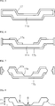
Zunächst werden, wie in
Anschließend wird, wie in
Das Halbleitersubstrat
Danach wird, wie in
Anschließend können, wie in
Danach wird, wie in
Dann wird, wie in
Anschließend wird, wie in
Danach können, wie in
Gemäß der ersten Ausführungsform kann, wie in
Danach kann, wie in
Anschließend kann, wie in
Danach kann, wie in
Die erste Metallschicht
Die erste und die zweite Metallschicht
Ein phosphoreszierender bzw. Leuchtstoff
Gemäß der Ausführungsform kann, wie in
Das zweite Halbleitersubstrat
Die erste leitfähige Schicht, welche die erste Metallschicht
Die erste leitfähige Schicht kann die erste Metallschicht
Die zweite leitfähige Schicht kann die zweite Metallschicht
Der Leuchtstoff
Gemäß der Ausführungsform kann eine Zener-Diode (nicht gezeigt) auf dem zweiten Halbleitersubstrat
In der Lichtemissionsvorrichtungsbaugruppe gemäß der Ausführungsform ist ein Montagebereich für das Lichtemissionsteil
Ferner können der Abstand zwischen einer reflektierenden Oberfläche, wie etw einer (111)-Oberfläche, die zwischen der ersten Oberfläche und der zweiten Oberfläche ausgebildet ist, und dem Lichtemissionsteil
Zweite AusführungsformSecond embodiment
Die Lichtemissionsvorrichtungsbaugruppe gemäß der zweiten Ausführungsform umfasst das zweite Halbleitersubstrat
Die zweite Ausführungsform kann die technischen Merkmale der ersten Ausführungsform verwenden, daher wird die zweite Ausführungsform unter Fokussierung auf die Merkmale, die sich von der ersten Ausführungsform unterscheiden, beschrieben werden.The second embodiment may use the technical features of the first embodiment, therefore, the second embodiment will be described with focus on the features different from the first embodiment.
Im Unterschied zur ersten Ausführungsform ist gemäß der zweiten Ausführungsform ein Leuchtstoff in dem zweiten Formteil
Gemäß der zweiten Ausführungsform, da das zweite Formteil
Dritte AusführungsformThird embodiment
Die dritte Ausführungsform kann die technischen Merkmale der ersten Ausführungsform verwenden, so dass die dritte Ausführungsform unter Fokussierung auf die Merkmale, die sich von der ersten Ausführungsform unterscheiden, beschrieben werden wird.The third embodiment may use the technical features of the first embodiment, so that the third embodiment will be described focusing on the features different from the first embodiment.
Im Vergleich mit dem ersten Ausführungsbeispiel verwendet die dritte Ausführungsform ein drittes Halbleitersubstrat
Gemäß der dritten Ausführungsform wird die V-förmige Vertiefung auf der ersten Oberfläche ausgebildet, so dass Licht, das nicht aus der Lichtemissionsvorrichtung Versandstücks entkommt, sondern in Richtung der ersten Oberfläche reflektiert wird, von einer konkav-konvexen Oberfläche mit einem geänderten Reflexionswinkel reflektiert, um die Wahrscheinlichkeit, mit der das Licht von der Lichtemissionsvorrichtungsbaugruppe emittiert wird, zu erhöhen. Daher kann eine Lichtausbeute weiter verbessert werden.According to the third embodiment, the V-shaped recess is formed on the first surface, so that light not coming out of the Light emission device escapes, but is reflected in the direction of the first surface, reflected by a concavo-convex surface with a changed reflection angle to increase the probability with which the light from the light emitting device assembly is emitted. Therefore, a luminous efficacy can be further improved.
Vierte AusführungsformFourth embodiment
Die vierte Ausführungsform kann die technischen Merkmale der zweiten Ausführungsform verwenden, so dass die vierte Ausführungsform unter Fokussierung auf die Merkmale, die sich von der zweiten Ausführungsform unterscheiden, beschrieben werden wird.The fourth embodiment may use the technical features of the second embodiment, so that the fourth embodiment will be described with focus on the features different from the second embodiment.
Im Unterschied zu der zweiten Ausführungsform kann gemäß der vierten Ausführungsform die erste Oberfläche des Halbleitersubstrats
Bei Ausbildung der zweiten Oberfläche des Halbleitersubstrats
Gemäß der vierten Ausführungsform ist die V-förmige Vertiefung auf der ersten Oberfläche ausgebildet, so dass Licht, das nicht aus der Lichtemissionsvorrichtungsbaugruppe entkommt, sondern in Richtung der ersten Oberfläche reflektiert wird, von einer konkav-konvexen Oberfläche mit einem geändert Reflexionswinkel reflektiert wird, um die Wahrscheinlichkeit, mit der das Licht von der Lichtemissionsvorrichtungsbaugruppe emittiert wird, zu erhöhen. Daher kann eine Lichtausbeute weiter verbessert werden.According to the fourth embodiment, the V-shaped recess is formed on the first surface so that light that does not escape from the light emitting device assembly but is reflected toward the first surface is reflected by a concavo-convex surface having a changed reflection angle increase the likelihood that the light will be emitted by the light emitting device assembly. Therefore, a luminous efficacy can be further improved.
Gemäß der vierten Ausführungsform enthält das zweite Formteil
Fünfte AusführungsformFifth embodiment
Die fünfte Ausführungsform kann die technischen Merkmale der ersten Ausführungsform verwenden, so dass die fünfte Ausführungsform unter Fokussierung auf die Merkmale, die sich von der ersten Ausführungsform unterscheiden, beschrieben werden wird.The fifth embodiment may use the technical features of the first embodiment, so that the fifth embodiment will be described focusing on the features different from the first embodiment.
Gemäß der fünften Ausführungsform weist die Lichtemissionsvorrichtungsbaugruppe ein Halbleitersubstrat
Im Vergleich mit dem ersten Ausführungsbeispiel weist die fünfte Ausführungsform einen Unterschied darin auf, dass ein erstes und ein zweites Durchgangsloch
Zum Beispiel kann die erste Metallschicht
Gemäß der fünften Ausführungsform wird bei Ausbildung der zweiten Oberfläche des Halbleitersubstrats
Ein wünschenswertes Ätzmaskenmuster wird auf der oberen und der unteren Oberfläche des Halbleitersubstrats
Gemäß der Ausführungsform ist die erste leitfähige Schicht mit der zweiten leitfähigen Schicht durch das erste Durchgangsloch
Sechste AusführungsformSixth embodiment
Die sechste Ausführungsform kann die technischen Merkmale der fünften Ausführungsform verwenden, so dass die sechste Ausführungsform unter Fokussierung auf die Merkmale, die sich von der fünften Ausführungsform unterscheiden, beschrieben werden wird.The sixth embodiment may use the technical features of the fifth embodiment, so that the sixth embodiment will be described with focus on the features different from the fifth embodiment.
Die Lichtemissionsvorrichtungsbaugruppe gemäß der sechsten Ausführungsform kann das Halbleitersubstrat
Im Vergleich mit der fünften Ausführungsform kann die sechste Ausführungsform das zweite Formteil
Gemäß der sechsten Ausführungsform enthält das zweite Formteil
Gemäß der sechsten Ausführungsform kann die erste leitfähige Schicht durch das erste Durchgangsloch
Siebte AusführungsformSeventh embodiment
Die siebte Ausführungsform kann die technischen Merkmale der fünften Ausführungsform verwenden, so dass die siebte Ausführungsform unter Fokussierung auf die Merkmale, die sich von der fünften Ausführungsform unterscheiden, beschrieben werden wird.The seventh embodiment may use the technical features of the fifth embodiment, so that the seventh embodiment will be described with focus on the features different from the fifth embodiment.
Im Vergleich mit der fünften Ausführungsform kann die siebte Ausführungsform das Halbleitersubstrat
Bei Ausbildung der zweiten Oberfläche des Halbleitersubstrats
Gemäß der siebten Ausführungsform kann die V-förmige Vertiefung in der ersten Oberfläche ausgebildet werden, so dass Licht, das nicht aus der Lichtemissionsvorrichtungsbaugruppe entkommt, sondern in Richtung der ersten Oberfläche reflektiert wird, von der konkav-konvexen Oberfläche mit einem geändert Reflexionswinkel reflektiert werden kann, um die Wahrscheinlichkeit, mit der das Licht von der Lichtemissionsvorrichtungsbaugruppe emittiert wird, zu erhöhen. Daher kann die Lichtausbeute weiter verbessert werden.According to the seventh embodiment, the V-shaped groove can be formed in the first surface so that light that does not escape from the light emitting device assembly but is reflected toward the first surface can be reflected by the concavo-convex surface at a changed reflection angle to increase the likelihood that the light from the light emitter assembly will be emitted. Therefore, the luminous efficacy can be further improved.
Achte AusführungsformEighth embodiment
Die achte Ausführungsform kann die technischen Merkmale der sechsten Ausführungsform verwenden, so dass die achte Ausführungsform unter Fokussierung auf die Merkmale, die sich von der sechsten Ausführungsform unterscheiden, beschrieben werden wird.The eighth embodiment may use the technical features of the sixth embodiment, so that the eighth embodiment will be described with focus on the features different from the sixth embodiment.
Im Vergleich mit der sechsten Ausführungsform kann die achte Ausführungsform das Halbleitersubstrat
Bei Ausbildung der zweiten Oberfläche des Halbleitersubstrats
Gemäß der achten Ausführungsform kann die V-förmige Vertiefung in der ersten Oberfläche ausgebildet werden, so dass Licht, das nicht aus der Lichtemissionsvorrichtungsbaugruppe entkommt, sondern in Richtung der ersten Oberfläche reflektiert wird, von der konkav-konvexen Oberfläche mit einem geänderten Reflexionswinkel reflektiert werden kann, um die Wahrscheinlichkeit, mit der das Licht von der Lichtemissionsvorrichtungsbaugruppe emittiert wird, zu erhöhen. Daher kann die Lichtausbeute weiter verbessert werden.According to the eighth embodiment, the V-shaped groove can be formed in the first surface so that light that does not escape from the light emitting device assembly but is reflected toward the first surface can be reflected from the concavo-convex surface with a changed reflection angle to increase the likelihood that the light from the light emitter assembly will be emitted. Therefore, the luminous efficacy can be further improved.
Gemäß der achten Ausführungsform kann das zweite Formteil
Wie oben beschrieben, kann in der Lichtemissionsvorrichtungsbaugruppe gemäß den Ausführungsformen die Lichtausbeute verbessert werden, und die Farbabweichung kann reduziert werden.As described above, in the light emitting device assembly according to the embodiments, the light output can be improved, and the color deviation can be reduced.
Obschon Ausführungsformen unter Bezugnahme auf eine Anzahl von beispielhaften Ausführungsformen beschrieben worden sind, sollte verstanden werden, dass von den Fachleuten zahlreiche andere Modifikationen und Ausführungsformen, die in den Geist und Umfang der Prinzipien dieser Offenbarung fallen, erdacht werden können. Insbesondere sind viele Abwandlungen und Modifikationen in den Bauteilen und/oder Anordnungen der den Gegenstand bildenden kombinierten Anordnung innerhalb des Umfangs der Offenbarung, der Zeichnungen und der beigefügten Ansprüche möglich. Zusätzlich zu Abwandlungen und Modifikationen in den Bauteilen und/oder Anordnungen werden alternative Verwendungen gleichfalls für den Fachmann offenbar sein.Although embodiments have been described with reference to a number of exemplary embodiments, it should be understood that those skilled in the art may devise numerous other modifications and embodiments that fall within the spirit and scope of the principles of this disclosure. In particular, many modifications and variations are possible in the components and / or arrangements of the combined assembly forming the subject matter within the scope of the disclosure, the drawings, and the appended claims. In addition to variations and modifications in the components and / or arrangements, alternative uses will also be apparent to those skilled in the art.
Claims (15)
Applications Claiming Priority (2)
| Application Number | Priority Date | Filing Date | Title |
|---|---|---|---|
| KR1020080048241A KR100992778B1 (en) | 2008-05-23 | 2008-05-23 | Light emitting device package and method for manufacturing the same |
| KR10-2008-0048241 | 2008-05-23 |
Publications (1)
| Publication Number | Publication Date |
|---|---|
| DE202009018878U1 true DE202009018878U1 (en) | 2014-03-12 |
Family
ID=41340649
Family Applications (1)
| Application Number | Title | Priority Date | Filing Date |
|---|---|---|---|
| DE202009018878.7U Expired - Lifetime DE202009018878U1 (en) | 2008-05-23 | 2009-04-01 | Light emitting device assembly |
Country Status (6)
| Country | Link |
|---|---|
| US (6) | US7982237B2 (en) |
| EP (2) | EP2672531B1 (en) |
| KR (1) | KR100992778B1 (en) |
| CN (1) | CN102077372A (en) |
| DE (1) | DE202009018878U1 (en) |
| WO (1) | WO2009142391A2 (en) |
Families Citing this family (42)
| Publication number | Priority date | Publication date | Assignee | Title |
|---|---|---|---|---|
| JP5148849B2 (en) * | 2006-07-27 | 2013-02-20 | スタンレー電気株式会社 | LED package, light emitting device using the same, and method of manufacturing LED package |
| JP2010219377A (en) * | 2009-03-18 | 2010-09-30 | Toshiba Corp | Semiconductor light-emitting device and method of manufacturing the same |
| US8530990B2 (en) * | 2009-07-20 | 2013-09-10 | Sunpower Corporation | Optoelectronic device with heat spreader unit |
| US8471289B2 (en) * | 2009-12-28 | 2013-06-25 | Sanyo Electric Co., Ltd. | Semiconductor laser device, optical pickup device and semiconductor device |
| KR101091304B1 (en) * | 2010-01-20 | 2011-12-07 | 엘지이노텍 주식회사 | Light emitting device package and its manufacturing method |
| KR101637581B1 (en) * | 2010-03-09 | 2016-07-07 | 엘지이노텍 주식회사 | Light emitting device package and fabricating method thereof |
| US8525213B2 (en) | 2010-03-30 | 2013-09-03 | Lg Innotek Co., Ltd. | Light emitting device having multiple cavities and light unit having the same |
| KR101028329B1 (en) * | 2010-04-28 | 2011-04-12 | 엘지이노텍 주식회사 | Light emitting device package and its manufacturing method |
| KR101039994B1 (en) | 2010-05-24 | 2011-06-09 | 엘지이노텍 주식회사 | Light emitting device and light unit having same |
| US8563849B2 (en) | 2010-08-03 | 2013-10-22 | Sunpower Corporation | Diode and heat spreader for solar module |
| KR101161984B1 (en) | 2010-08-20 | 2012-07-03 | 엘지이노텍 주식회사 | Light-emitting element package |
| US20120112237A1 (en) * | 2010-11-05 | 2012-05-10 | Shenzhen China Star Optoelectronics Technology Co. Ltd. | Led package structure |
| KR20120105146A (en) * | 2011-03-15 | 2012-09-25 | 삼성전자주식회사 | Light emitting device package manufacturing apparatus and light emitting device manufacturing method using the same |
| CN102694081B (en) * | 2011-03-21 | 2014-11-05 | 展晶科技(深圳)有限公司 | Method for manufacturing light emitting diode |
| KR101255121B1 (en) * | 2011-08-10 | 2013-04-22 | 장종진 | Lighting emitting diode package and Method for manufacturing the same |
| KR20130022052A (en) * | 2011-08-24 | 2013-03-06 | 엘지이노텍 주식회사 | The light emitting device package and the light emitting system |
| JP5985322B2 (en) * | 2012-03-23 | 2016-09-06 | 株式会社東芝 | Semiconductor light emitting device and manufacturing method thereof |
| CN102903838A (en) * | 2012-07-10 | 2013-01-30 | 贵州大学 | Packaged LED light source with radiating structure and production method thereof |
| US8636198B1 (en) | 2012-09-28 | 2014-01-28 | Sunpower Corporation | Methods and structures for forming and improving solder joint thickness and planarity control features for solar cells |
| DE102013203759A1 (en) * | 2013-03-05 | 2014-09-11 | Osram Opto Semiconductors Gmbh | Optoelectronic component and electronic device with optoelectronic component |
| TW201442290A (en) * | 2013-04-24 | 2014-11-01 | 鴻海精密工業股份有限公司 | Light-emitting diode module |
| KR102221599B1 (en) * | 2014-06-18 | 2021-03-02 | 엘지이노텍 주식회사 | Light Emitting Device Package |
| US10249599B2 (en) | 2016-06-29 | 2019-04-02 | eLux, Inc. | Laminated printed color conversion phosphor sheets |
| US9755110B1 (en) | 2016-07-27 | 2017-09-05 | Sharp Laboratories Of America, Inc. | Substrate with topological features for steering fluidic assembly LED disks |
| US9985190B2 (en) | 2016-05-18 | 2018-05-29 | eLux Inc. | Formation and structure of post enhanced diodes for orientation control |
| US9722145B2 (en) | 2015-06-24 | 2017-08-01 | Sharp Laboratories Of America, Inc. | Light emitting device and fluidic manufacture thereof |
| US9892944B2 (en) | 2016-06-23 | 2018-02-13 | Sharp Kabushiki Kaisha | Diodes offering asymmetric stability during fluidic assembly |
| US9917226B1 (en) | 2016-09-15 | 2018-03-13 | Sharp Kabushiki Kaisha | Substrate features for enhanced fluidic assembly of electronic devices |
| CN104752586A (en) * | 2015-03-27 | 2015-07-01 | 华南理工大学 | LED graphic optimized packaging substrate, LED packaging member and manufacture method thereof |
| KR102503215B1 (en) | 2016-03-28 | 2023-02-24 | 삼성전자 주식회사 | Light emitting device package |
| JP6477734B2 (en) * | 2016-06-30 | 2019-03-06 | 日亜化学工業株式会社 | Light emitting device and manufacturing method thereof |
| US9627437B1 (en) | 2016-06-30 | 2017-04-18 | Sharp Laboratories Of America, Inc. | Patterned phosphors in through hole via (THV) glass |
| US10243097B2 (en) | 2016-09-09 | 2019-03-26 | eLux Inc. | Fluidic assembly using tunable suspension flow |
| US10378736B2 (en) * | 2016-11-03 | 2019-08-13 | Foshan Nationstar Optoelectronics Co., Ltd. | LED bracket, LED bracket array, LED device and LED display screen |
| US9837390B1 (en) | 2016-11-07 | 2017-12-05 | Corning Incorporated | Systems and methods for creating fluidic assembly structures on a substrate |
| KR102716558B1 (en) * | 2019-04-30 | 2024-10-15 | 엘지전자 주식회사 | Display device using semiconductor light emitting diode |
| DE102019207713B4 (en) * | 2019-05-27 | 2024-12-12 | Würth Elektronik eiSos Gmbh & Co. KG | Arrangement with an LED component and method for establishing a connection |
| DE102019207714B4 (en) * | 2019-05-27 | 2024-12-12 | Würth Elektronik eiSos Gmbh & Co. KG | Arrangement with an SMD component and method for producing a connection |
| JP7469592B2 (en) | 2019-12-05 | 2024-04-17 | 日亜化学工業株式会社 | Light-emitting device |
| JP2021110161A (en) * | 2020-01-10 | 2021-08-02 | 株式会社オーイケ | Wall module and structure having the same |
| CN111613704B (en) * | 2020-05-29 | 2021-05-18 | 黄山博蓝特半导体科技有限公司 | A kind of patterned sapphire substrate for high-brightness deep ultraviolet LED and preparation method thereof |
| DE102021100546A1 (en) * | 2021-01-13 | 2022-07-14 | OSRAM Opto Semiconductors Gesellschaft mit beschränkter Haftung | OPTOELECTRONIC SEMICONDUCTOR COMPONENT, OPTOELECTRONIC DEVICE, AND METHOD FOR MANUFACTURING AN OPTOELECTRONIC SEMICONDUCTOR COMPONENT AND/OR AN OPTOELECTRONIC DEVICE |
Family Cites Families (110)
| Publication number | Priority date | Publication date | Assignee | Title |
|---|---|---|---|---|
| US5032896A (en) * | 1989-08-31 | 1991-07-16 | Hughes Aircraft Company | 3-D integrated circuit assembly employing discrete chips |
| US5291038A (en) * | 1990-12-19 | 1994-03-01 | Sharp Kabushiki Kaisha | Reflective type photointerrupter |
| DE4242842C2 (en) * | 1992-02-14 | 1999-11-04 | Sharp Kk | Light-emitting component for surface mounting and method for its production |
| US5412748A (en) * | 1992-12-04 | 1995-05-02 | Kabushiki Kaisha Toshiba | Optical semiconductor module |
| US5474958A (en) * | 1993-05-04 | 1995-12-12 | Motorola, Inc. | Method for making semiconductor device having no die supporting surface |
| JP2914097B2 (en) * | 1993-06-25 | 1999-06-28 | 松下電工株式会社 | Injection molded printed circuit board |
| JPH08274378A (en) | 1995-03-30 | 1996-10-18 | Kyocera Corp | Light emitting device storage package |
| JPH10319871A (en) * | 1997-05-19 | 1998-12-04 | Kouha:Kk | LED display device |
| JPH1131751A (en) * | 1997-07-10 | 1999-02-02 | Sony Corp | Hollow package and manufacturing method thereof |
| JP2001257410A (en) | 2000-03-09 | 2001-09-21 | Kyocera Corp | Electronic components |
| US6600231B2 (en) * | 2000-05-11 | 2003-07-29 | Mitutoyo Corporation | Functional device unit and method of producing the same |
| DE10041686A1 (en) * | 2000-08-24 | 2002-03-14 | Osram Opto Semiconductors Gmbh | Component with a large number of LED chips |
| KR20020037623A (en) | 2000-11-15 | 2002-05-22 | 윤종용 | Semiconductor chip package having glass lids and grooved loading parts |
| US6583447B2 (en) * | 2001-08-27 | 2003-06-24 | Harvatek Corp. | Multiple LED chip package |
| JP4067801B2 (en) * | 2001-09-18 | 2008-03-26 | 松下電器産業株式会社 | Lighting device |
| US20050073846A1 (en) * | 2001-09-27 | 2005-04-07 | Kenji Takine | Lightemitting device and method of manufacturing the same |
| US6531328B1 (en) * | 2001-10-11 | 2003-03-11 | Solidlite Corporation | Packaging of light-emitting diode |
| JP4269709B2 (en) | 2002-02-19 | 2009-05-27 | 日亜化学工業株式会社 | Light emitting device and manufacturing method thereof |
| US6924514B2 (en) * | 2002-02-19 | 2005-08-02 | Nichia Corporation | Light-emitting device and process for producing thereof |
| JP4280038B2 (en) * | 2002-08-05 | 2009-06-17 | 日亜化学工業株式会社 | Light emitting device |
| WO2003080764A1 (en) | 2002-03-22 | 2003-10-02 | Nichia Corporation | Nitride phosphor and method for preparation thereof, and light emitting device |
| JP4407204B2 (en) | 2002-08-30 | 2010-02-03 | 日亜化学工業株式会社 | Light emitting device |
| JP2004207542A (en) | 2002-12-26 | 2004-07-22 | Kyocera Corp | Light emitting element storage package and light emitting device |
| JP4009208B2 (en) | 2003-01-21 | 2007-11-14 | 京セラ株式会社 | Light emitting device |
| JP2004281994A (en) | 2003-01-24 | 2004-10-07 | Kyocera Corp | Light emitting element storage package and light emitting device |
| JP2004253711A (en) | 2003-02-21 | 2004-09-09 | Kyocera Corp | Light emitting element storage package and light emitting device |
| KR100517841B1 (en) * | 2003-02-22 | 2005-09-30 | 주식회사 엠에스솔루션 | FBAR band pass filter, Duplexer having the FBAR band pass filter and Methods for manufacturing the same |
| US6835960B2 (en) * | 2003-03-03 | 2004-12-28 | Opto Tech Corporation | Light emitting diode package structure |
| CN102290409B (en) * | 2003-04-01 | 2014-01-15 | 夏普株式会社 | Light-emitting apparatus |
| JP4070208B2 (en) | 2003-04-21 | 2008-04-02 | 京セラ株式会社 | Light emitting element storage package and light emitting device |
| JP2004327504A (en) * | 2003-04-21 | 2004-11-18 | Kyocera Corp | Light emitting element storage package and light emitting device |
| US7312101B2 (en) * | 2003-04-22 | 2007-12-25 | Micron Technology, Inc. | Packaged microelectronic devices and methods for packaging microelectronic devices |
| US7095053B2 (en) * | 2003-05-05 | 2006-08-22 | Lamina Ceramics, Inc. | Light emitting diodes packaged for high temperature operation |
| EP1627437B1 (en) * | 2003-05-26 | 2016-03-30 | Panasonic Intellectual Property Management Co., Ltd. | Light-emitting device |
| JP4645071B2 (en) * | 2003-06-20 | 2011-03-09 | 日亜化学工業株式会社 | Package molded body and semiconductor device using the same |
| US7183587B2 (en) * | 2003-09-09 | 2007-02-27 | Cree, Inc. | Solid metal block mounting substrates for semiconductor light emitting devices |
| TWI236103B (en) * | 2003-10-28 | 2005-07-11 | South Epitaxy Corp | Flip-chip LED package structure |
| US7652381B2 (en) * | 2003-11-13 | 2010-01-26 | Interconnect Portfolio Llc | Interconnect system without through-holes |
| KR100540848B1 (en) * | 2004-01-02 | 2006-01-11 | 주식회사 메디아나전자 | White light emitting diode device composed of double mold and manufacturing method |
| JP4572312B2 (en) * | 2004-02-23 | 2010-11-04 | スタンレー電気株式会社 | LED and manufacturing method thereof |
| JP4504056B2 (en) * | 2004-03-22 | 2010-07-14 | スタンレー電気株式会社 | Manufacturing method of semiconductor light emitting device |
| US7326583B2 (en) | 2004-03-31 | 2008-02-05 | Cree, Inc. | Methods for packaging of a semiconductor light emitting device |
| JP4471356B2 (en) | 2004-04-23 | 2010-06-02 | スタンレー電気株式会社 | Semiconductor light emitting device |
| KR100927256B1 (en) | 2004-07-09 | 2009-11-16 | 엘지전자 주식회사 | Method of fabricating a zener diode integrated sub-mount |
| TWI240438B (en) * | 2004-09-07 | 2005-09-21 | Opto Tech Corp | High power LED array |
| JP4254669B2 (en) * | 2004-09-07 | 2009-04-15 | 豊田合成株式会社 | Light emitting device |
| JP2006114854A (en) * | 2004-10-18 | 2006-04-27 | Sharp Corp | Backlight device for semiconductor light emitting device and liquid crystal display device |
| US20060097385A1 (en) * | 2004-10-25 | 2006-05-11 | Negley Gerald H | Solid metal block semiconductor light emitting device mounting substrates and packages including cavities and heat sinks, and methods of packaging same |
| EP1816685A4 (en) | 2004-10-27 | 2010-01-13 | Kyocera Corp | LIGHT - EMITTING ELEMENT MOUNTING PLATE, LIGHT - EMITTING ELEMENT STORAGE PACKAGE, LIGHT - EMITTING DEVICE, AND LIGHTING EQUIPMENT |
| JP2008012930A (en) | 2004-10-27 | 2008-01-24 | Aisin Seiki Co Ltd | Sheet device |
| US7551141B1 (en) * | 2004-11-08 | 2009-06-23 | Alien Technology Corporation | RFID strap capacitively coupled and method of making same |
| JP2006135225A (en) | 2004-11-09 | 2006-05-25 | Toshiba Corp | Light emitting device |
| JP4061409B2 (en) * | 2004-11-09 | 2008-03-19 | 国立大学法人九州大学 | Sensor unit and biosensor |
| JP2008523637A (en) * | 2004-12-14 | 2008-07-03 | ソウル オプト−デバイス カンパニー リミテッド | Light emitting device having a plurality of light emitting cells and package mounting the same |
| JP3872490B2 (en) | 2004-12-24 | 2007-01-24 | 京セラ株式会社 | Light emitting element storage package, light emitting device, and lighting device |
| TWI239670B (en) * | 2004-12-29 | 2005-09-11 | Ind Tech Res Inst | Package structure of light emitting diode and its manufacture method |
| TWI269423B (en) * | 2005-02-02 | 2006-12-21 | Phoenix Prec Technology Corp | Substrate assembly with direct electrical connection as a semiconductor package |
| US7411225B2 (en) * | 2005-03-21 | 2008-08-12 | Lg Electronics Inc. | Light source apparatus |
| KR100593935B1 (en) * | 2005-03-24 | 2006-06-30 | 삼성전기주식회사 | Light emitting diode package and manufacturing method thereof |
| KR100593943B1 (en) * | 2005-04-30 | 2006-06-30 | 삼성전기주식회사 | Manufacturing method of light emitting diode package |
| JP2007049114A (en) * | 2005-05-30 | 2007-02-22 | Sharp Corp | Light emitting device and manufacturing method thereof |
| TWI311820B (en) * | 2005-06-07 | 2009-07-01 | Fujikura Ltd | Substrate for mounting light-emitting element, light-emitting element module, iluumination apparatus, display apparatus, and traffic signal device |
| JP2007033698A (en) * | 2005-07-25 | 2007-02-08 | Fuji Xerox Co Ltd | Submount for mounting optical components, and optical transceiver module |
| US20070031992A1 (en) * | 2005-08-05 | 2007-02-08 | Schatz Kenneth D | Apparatuses and methods facilitating functional block deposition |
| KR100600411B1 (en) | 2005-08-26 | 2006-07-19 | 엘지전자 주식회사 | Light emitting device package and manufacturing method thereof |
| US7719099B2 (en) * | 2005-10-21 | 2010-05-18 | Advanced Optoelectronic Technology Inc. | Package structure for solid-state lighting devices and method of fabricating the same |
| KR101171186B1 (en) * | 2005-11-10 | 2012-08-06 | 삼성전자주식회사 | High luminance light emitting diode and liquid crystal display panel of using the same |
| JP2007157940A (en) * | 2005-12-02 | 2007-06-21 | Nichia Chem Ind Ltd | Light emitting device and method for manufacturing light emitting device |
| JP2007184426A (en) * | 2006-01-06 | 2007-07-19 | Shinko Electric Ind Co Ltd | Manufacturing method of semiconductor device |
| JP4817931B2 (en) | 2006-03-31 | 2011-11-16 | 京セラ株式会社 | Light emitting device and light emitting module |
| JP4925673B2 (en) | 2006-01-31 | 2012-05-09 | 京セラ株式会社 | Light emitting device and light emitting module |
| JP2007231253A (en) * | 2006-01-31 | 2007-09-13 | Asahi Glass Co Ltd | Translucent sealing curable resin composition, resin-sealed light emitting device, and method for producing the same |
| US7928462B2 (en) | 2006-02-16 | 2011-04-19 | Lg Electronics Inc. | Light emitting device having vertical structure, package thereof and method for manufacturing the same |
| JP2007234846A (en) | 2006-03-01 | 2007-09-13 | Ngk Spark Plug Co Ltd | Ceramic package for light emitting device |
| KR100836210B1 (en) | 2006-03-22 | 2008-06-09 | (주) 아모센스 | Semiconductor package and manufacturing method thereof |
| JP2007273592A (en) | 2006-03-30 | 2007-10-18 | Kyocera Corp | Light-emitting element wiring board and light-emitting device |
| JP4960645B2 (en) | 2006-03-30 | 2012-06-27 | 京セラ株式会社 | Wavelength converter and light emitting device |
| JP5091421B2 (en) * | 2006-04-07 | 2012-12-05 | 株式会社東芝 | Semiconductor light emitting device |
| KR100735310B1 (en) * | 2006-04-21 | 2007-07-04 | 삼성전기주식회사 | LED package having multilayer reflective surface structure and manufacturing method thereof |
| JP2007305703A (en) | 2006-05-10 | 2007-11-22 | Nichia Chem Ind Ltd | Light emitting device |
| JP2007305785A (en) * | 2006-05-11 | 2007-11-22 | Nichia Chem Ind Ltd | Light emitting device |
| JP4943739B2 (en) * | 2006-05-18 | 2012-05-30 | 浜松ホトニクス株式会社 | Optical transceiver device |
| KR100854328B1 (en) * | 2006-07-07 | 2008-08-28 | 엘지전자 주식회사 | Light emitting device package and its manufacturing method |
| US7960819B2 (en) | 2006-07-13 | 2011-06-14 | Cree, Inc. | Leadframe-based packages for solid state emitting devices |
| TWI320237B (en) * | 2006-07-24 | 2010-02-01 | Si-substrate and structure of opto-electronic package having the same | |
| JP2008053702A (en) | 2006-07-26 | 2008-03-06 | Kyocera Corp | Light emitting device and lighting device |
| JP4841348B2 (en) | 2006-07-27 | 2011-12-21 | 京セラ株式会社 | WIRING BOARD FOR LIGHT EMITTING ELEMENT AND LIGHT EMITTING DEVICE |
| JP5148849B2 (en) * | 2006-07-27 | 2013-02-20 | スタンレー電気株式会社 | LED package, light emitting device using the same, and method of manufacturing LED package |
| US20080029775A1 (en) * | 2006-08-02 | 2008-02-07 | Lustrous Technology Ltd. | Light emitting diode package with positioning groove |
| JP5250949B2 (en) * | 2006-08-07 | 2013-07-31 | デクセリアルズ株式会社 | Light emitting element module |
| KR100792342B1 (en) | 2006-08-23 | 2008-01-07 | 동부일렉트로닉스 주식회사 | Image sensor manufacturing method |
| US7635869B2 (en) * | 2006-09-14 | 2009-12-22 | Lumination Llc | Support with recessed electrically conductive chip attachment material for flip-chip bonding a light emitting chip |
| TWI338385B (en) * | 2006-12-13 | 2011-03-01 | Silicon Base Dev Inc | Side light package structure of light diode and its producing method |
| KR100845856B1 (en) * | 2006-12-21 | 2008-07-14 | 엘지전자 주식회사 | Light emitting device package and its manufacturing method |
| KR100818518B1 (en) * | 2007-03-14 | 2008-03-31 | 삼성전기주식회사 | LED Package |
| US20080237621A1 (en) * | 2007-03-30 | 2008-10-02 | Sharp Kabushiki Kaisha | Light emitting device and method of producing the same |
| JP5441316B2 (en) * | 2007-04-05 | 2014-03-12 | ローム株式会社 | Semiconductor light emitting device |
| CN201066688Y (en) * | 2007-05-11 | 2008-05-28 | 群康科技(深圳)有限公司 | LED and backlight module |
| US7911059B2 (en) * | 2007-06-08 | 2011-03-22 | SeniLEDS Optoelectronics Co., Ltd | High thermal conductivity substrate for a semiconductor device |
| CN101325193B (en) * | 2007-06-13 | 2010-06-09 | 先进开发光电股份有限公司 | LED package |
| US20090023234A1 (en) * | 2007-07-17 | 2009-01-22 | Hung-Tsung Hsu | Method for manufacturing light emitting diode package |
| US8212279B2 (en) * | 2008-03-25 | 2012-07-03 | Bridge Semiconductor Corporation | Semiconductor chip assembly with post/base heat spreader, signal post and cavity |
| US8415703B2 (en) * | 2008-03-25 | 2013-04-09 | Bridge Semiconductor Corporation | Semiconductor chip assembly with post/base/flange heat spreader and cavity in flange |
| US8324723B2 (en) | 2008-03-25 | 2012-12-04 | Bridge Semiconductor Corporation | Semiconductor chip assembly with bump/base heat spreader and dual-angle cavity in bump |
| US8288792B2 (en) * | 2008-03-25 | 2012-10-16 | Bridge Semiconductor Corporation | Semiconductor chip assembly with post/base/post heat spreader |
| US20100001305A1 (en) * | 2008-07-07 | 2010-01-07 | Visera Technologies Company Limited | Semiconductor devices and fabrication methods thereof |
| US7928458B2 (en) * | 2008-07-15 | 2011-04-19 | Visera Technologies Company Limited | Light-emitting diode device and method for fabricating the same |
| US7932529B2 (en) * | 2008-08-28 | 2011-04-26 | Visera Technologies Company Limited | Light-emitting diode device and method for fabricating the same |
| US7807484B2 (en) * | 2008-10-15 | 2010-10-05 | Visera Technologies Company Limited | Light-emitting diode device and method for fabricating the same |
| US7928655B2 (en) * | 2008-11-10 | 2011-04-19 | Visera Technologies Company Limited | Light-emitting diode device and method for fabricating the same |
-
2008
- 2008-05-23 KR KR1020080048241A patent/KR100992778B1/en not_active Expired - Fee Related
-
2009
- 2009-04-01 CN CN2009801251818A patent/CN102077372A/en active Pending
- 2009-04-01 EP EP13183420.2A patent/EP2672531B1/en not_active Not-in-force
- 2009-04-01 DE DE202009018878.7U patent/DE202009018878U1/en not_active Expired - Lifetime
- 2009-04-01 EP EP09750713.1A patent/EP2299503A4/en not_active Withdrawn
- 2009-04-01 WO PCT/KR2009/001665 patent/WO2009142391A2/en not_active Ceased
- 2009-05-22 US US12/470,787 patent/US7982237B2/en active Active
-
2011
- 2011-06-21 US US13/165,741 patent/US8125000B2/en not_active Expired - Fee Related
-
2012
- 2012-01-10 US US13/347,475 patent/US8592855B2/en not_active Expired - Fee Related
-
2013
- 2013-09-09 US US14/021,577 patent/US8878229B2/en active Active
-
2014
- 2014-10-07 US US14/508,790 patent/US9190450B2/en not_active Expired - Fee Related
-
2015
- 2015-10-26 US US14/923,229 patent/US9455375B2/en active Active
Also Published As
| Publication number | Publication date |
|---|---|
| KR20090122044A (en) | 2009-11-26 |
| EP2672531A3 (en) | 2014-03-05 |
| US8592855B2 (en) | 2013-11-26 |
| WO2009142391A2 (en) | 2009-11-26 |
| US8878229B2 (en) | 2014-11-04 |
| WO2009142391A3 (en) | 2010-01-14 |
| EP2672531A2 (en) | 2013-12-11 |
| US8125000B2 (en) | 2012-02-28 |
| US20160049548A1 (en) | 2016-02-18 |
| US20110248311A1 (en) | 2011-10-13 |
| US9190450B2 (en) | 2015-11-17 |
| US7982237B2 (en) | 2011-07-19 |
| KR100992778B1 (en) | 2010-11-05 |
| EP2299503A2 (en) | 2011-03-23 |
| EP2672531B1 (en) | 2020-04-29 |
| US20120104447A1 (en) | 2012-05-03 |
| US9455375B2 (en) | 2016-09-27 |
| CN102077372A (en) | 2011-05-25 |
| US20090289272A1 (en) | 2009-11-26 |
| EP2299503A4 (en) | 2014-02-05 |
| US20140008696A1 (en) | 2014-01-09 |
| US20150021646A1 (en) | 2015-01-22 |
Similar Documents
| Publication | Publication Date | Title |
|---|---|---|
| DE202009018878U1 (en) | Light emitting device assembly | |
| DE102016119002B4 (en) | OPTOELECTRONIC DEVICE AND METHOD FOR MANUFACTURING OPTOELECTRONIC DEVICE | |
| DE112011103186B4 (en) | Light-emitting diode unit on wafer level | |
| WO2020169524A1 (en) | Optoelectronic semiconductor component, and method for producing optoelectronic semiconductor components | |
| DE112009001543B4 (en) | Manufacture of compact optoelectronic assemblies | |
| DE202008018233U1 (en) | Housing for a light-emitting device | |
| DE202009018568U1 (en) | Light emitting diode and light emitting device | |
| DE102015114849A1 (en) | Method for producing light-emitting diode filaments and light-emitting filament | |
| DE102005008339A1 (en) | Light-emitting diode (LED) and manufacturing method therefor | |
| DE102014112540A1 (en) | Optoelectronic component | |
| DE102009025015A1 (en) | Light-emitting device and method for its production | |
| DE202010017509U1 (en) | Light emitting device and lighting system | |
| DE202014011201U1 (en) | Semiconductor light-emitting device with metallized sidewalls | |
| DE102018129068A1 (en) | Light emitting device and method of making the same | |
| WO2014048830A1 (en) | Optoelectronic component | |
| DE112014005652B4 (en) | Optoelectronic component and process | |
| DE102012109995A1 (en) | Semiconductor component e.g. laser diode chip has contact portion that is provided for externally and electrically contacting semiconductor component with bonding compound, and patterning portion that is provided with elongated recess | |
| DE102015007750A1 (en) | Light emitting diode arrangement and method for producing a light emitting diode array | |
| DE102019218501A1 (en) | COMPONENT FOR A DISPLAY AND METHOD FOR MANUFACTURING A COMPONENT | |
| DE102014208958A1 (en) | Surface-mountable optoelectronic component and method for producing a surface-mountable optoelectronic component | |
| WO2016188702A1 (en) | Method for producing an electronic component with a carrier element and electronic component with a carrier element | |
| WO2022100976A1 (en) | Optoelectronic semiconductor component and method for producing same | |
| DE102024104316A1 (en) | LIGHT-EMITTING DEVICE | |
| DE102019106546A1 (en) | METHOD FOR MANUFACTURING OPTOELECTRONIC SEMICONDUCTOR COMPONENTS AND OPTOELECTRONIC SEMICONDUCTOR COMPONENTS | |
| DE102018120637A1 (en) | CIRCUIT BOARD AND METHOD FOR PRODUCING A CIRCUIT BOARD WITH AT LEAST ONE OPTOELECTRONIC COMPONENT INTEGRATED INTO THE CIRCUIT BOARD |
Legal Events
| Date | Code | Title | Description |
|---|---|---|---|
| R150 | Utility model maintained after payment of first maintenance fee after three years | ||
| R207 | Utility model specification |
Effective date: 20140417 |
|
| R150 | Utility model maintained after payment of first maintenance fee after three years |
Effective date: 20140404 |
|
| R151 | Utility model maintained after payment of second maintenance fee after six years | ||
| R151 | Utility model maintained after payment of second maintenance fee after six years |
Effective date: 20150318 |
|
| R152 | Utility model maintained after payment of third maintenance fee after eight years | ||
| R071 | Expiry of right |