DE102004059389B4 - Semiconductor device with compensation metallization - Google Patents
Semiconductor device with compensation metallization Download PDFInfo
- Publication number
- DE102004059389B4 DE102004059389B4 DE102004059389A DE102004059389A DE102004059389B4 DE 102004059389 B4 DE102004059389 B4 DE 102004059389B4 DE 102004059389 A DE102004059389 A DE 102004059389A DE 102004059389 A DE102004059389 A DE 102004059389A DE 102004059389 B4 DE102004059389 B4 DE 102004059389B4
- Authority
- DE
- Germany
- Prior art keywords
- contact surface
- metallization
- vertical
- component according
- semiconductor component
- Prior art date
- Legal status (The legal status is an assumption and is not a legal conclusion. Google has not performed a legal analysis and makes no representation as to the accuracy of the status listed.)
- Expired - Fee Related
Links
Images


Classifications
-
- H—ELECTRICITY
- H10—SEMICONDUCTOR DEVICES; ELECTRIC SOLID-STATE DEVICES NOT OTHERWISE PROVIDED FOR
- H10W—GENERIC PACKAGES, INTERCONNECTIONS, CONNECTORS OR OTHER CONSTRUCTIONAL DETAILS OF DEVICES COVERED BY CLASS H10
- H10W72/00—Interconnections or connectors in packages
- H10W72/50—Bond wires
-
- H—ELECTRICITY
- H10—SEMICONDUCTOR DEVICES; ELECTRIC SOLID-STATE DEVICES NOT OTHERWISE PROVIDED FOR
- H10W—GENERIC PACKAGES, INTERCONNECTIONS, CONNECTORS OR OTHER CONSTRUCTIONAL DETAILS OF DEVICES COVERED BY CLASS H10
- H10W72/00—Interconnections or connectors in packages
- H10W72/071—Connecting or disconnecting
- H10W72/075—Connecting or disconnecting of bond wires
- H10W72/07531—Techniques
- H10W72/07536—Soldering or alloying
-
- H—ELECTRICITY
- H10—SEMICONDUCTOR DEVICES; ELECTRIC SOLID-STATE DEVICES NOT OTHERWISE PROVIDED FOR
- H10W—GENERIC PACKAGES, INTERCONNECTIONS, CONNECTORS OR OTHER CONSTRUCTIONAL DETAILS OF DEVICES COVERED BY CLASS H10
- H10W72/00—Interconnections or connectors in packages
- H10W72/50—Bond wires
- H10W72/531—Shapes of wire connectors
- H10W72/5363—Shapes of wire connectors the connected ends being wedge-shaped
-
- H—ELECTRICITY
- H10—SEMICONDUCTOR DEVICES; ELECTRIC SOLID-STATE DEVICES NOT OTHERWISE PROVIDED FOR
- H10W—GENERIC PACKAGES, INTERCONNECTIONS, CONNECTORS OR OTHER CONSTRUCTIONAL DETAILS OF DEVICES COVERED BY CLASS H10
- H10W72/00—Interconnections or connectors in packages
- H10W72/50—Bond wires
- H10W72/541—Dispositions of bond wires
- H10W72/5434—Dispositions of bond wires the connected ends being on auxiliary connecting means on bond pads, e.g. on other bond wires
-
- H—ELECTRICITY
- H10—SEMICONDUCTOR DEVICES; ELECTRIC SOLID-STATE DEVICES NOT OTHERWISE PROVIDED FOR
- H10W—GENERIC PACKAGES, INTERCONNECTIONS, CONNECTORS OR OTHER CONSTRUCTIONAL DETAILS OF DEVICES COVERED BY CLASS H10
- H10W72/00—Interconnections or connectors in packages
- H10W72/50—Bond wires
- H10W72/551—Materials of bond wires
- H10W72/552—Materials of bond wires comprising metals or metalloids, e.g. silver
- H10W72/5525—Materials of bond wires comprising metals or metalloids, e.g. silver comprising copper [Cu]
-
- H—ELECTRICITY
- H10—SEMICONDUCTOR DEVICES; ELECTRIC SOLID-STATE DEVICES NOT OTHERWISE PROVIDED FOR
- H10W—GENERIC PACKAGES, INTERCONNECTIONS, CONNECTORS OR OTHER CONSTRUCTIONAL DETAILS OF DEVICES COVERED BY CLASS H10
- H10W72/00—Interconnections or connectors in packages
- H10W72/50—Bond wires
- H10W72/59—Bond pads specially adapted therefor
-
- H—ELECTRICITY
- H10—SEMICONDUCTOR DEVICES; ELECTRIC SOLID-STATE DEVICES NOT OTHERWISE PROVIDED FOR
- H10W—GENERIC PACKAGES, INTERCONNECTIONS, CONNECTORS OR OTHER CONSTRUCTIONAL DETAILS OF DEVICES COVERED BY CLASS H10
- H10W72/00—Interconnections or connectors in packages
- H10W72/851—Dispositions of multiple connectors or interconnections
- H10W72/874—On different surfaces
- H10W72/884—Die-attach connectors and bond wires
-
- H—ELECTRICITY
- H10—SEMICONDUCTOR DEVICES; ELECTRIC SOLID-STATE DEVICES NOT OTHERWISE PROVIDED FOR
- H10W—GENERIC PACKAGES, INTERCONNECTIONS, CONNECTORS OR OTHER CONSTRUCTIONAL DETAILS OF DEVICES COVERED BY CLASS H10
- H10W72/00—Interconnections or connectors in packages
- H10W72/90—Bond pads, in general
- H10W72/921—Structures or relative sizes of bond pads
- H10W72/923—Bond pads having multiple stacked layers
-
- H—ELECTRICITY
- H10—SEMICONDUCTOR DEVICES; ELECTRIC SOLID-STATE DEVICES NOT OTHERWISE PROVIDED FOR
- H10W—GENERIC PACKAGES, INTERCONNECTIONS, CONNECTORS OR OTHER CONSTRUCTIONAL DETAILS OF DEVICES COVERED BY CLASS H10
- H10W72/00—Interconnections or connectors in packages
- H10W72/90—Bond pads, in general
- H10W72/931—Shapes of bond pads
- H10W72/932—Plan-view shape, i.e. in top view
-
- H—ELECTRICITY
- H10—SEMICONDUCTOR DEVICES; ELECTRIC SOLID-STATE DEVICES NOT OTHERWISE PROVIDED FOR
- H10W—GENERIC PACKAGES, INTERCONNECTIONS, CONNECTORS OR OTHER CONSTRUCTIONAL DETAILS OF DEVICES COVERED BY CLASS H10
- H10W72/00—Interconnections or connectors in packages
- H10W72/90—Bond pads, in general
- H10W72/951—Materials of bond pads
- H10W72/952—Materials of bond pads comprising metals or metalloids, e.g. PbSn, Ag or Cu
-
- H—ELECTRICITY
- H10—SEMICONDUCTOR DEVICES; ELECTRIC SOLID-STATE DEVICES NOT OTHERWISE PROVIDED FOR
- H10W—GENERIC PACKAGES, INTERCONNECTIONS, CONNECTORS OR OTHER CONSTRUCTIONAL DETAILS OF DEVICES COVERED BY CLASS H10
- H10W74/00—Encapsulations, e.g. protective coatings
Landscapes
- Internal Circuitry In Semiconductor Integrated Circuit Devices (AREA)
Abstract
Halbleiterbauelement mit einem eine erste Kontaktfläche (41) aufweisenden Halbleiterkörper (40) und einem eine zweite Kontaktfläche (52) aufweisenden Anschlusselement (50, 50a, 50b, 50c, 50d), wobei das Anschlusselement (50, 50a, 50b, 50c, 50d) als Bonddraht oder als Anschlussclip oder als Leiterbahn ausgebildet ist, die erste Kontaktfläche (41) und die zweite Kontaktfläche (52) in einer vertikalen Richtung (v) voneinander beabstandet sind, die erste Kontaktfläche (41) in einer horizontalen Richtung (r, r1, r2) einen ersten Rand (411) und die zweite Kontaktfläche (52) in der horizontalen Richtung (r, r1, r2) einen zweiten Rand aufweist, zwischen der ersten Kontaktfläche (41) und der zweiten Kontaktfläche (52) eine Ausgleichsmetallisierung (10) angeordnet ist, die zum Ausgleich thermomechanischer Spannungen dient, und die die erste Kontaktfläche (41) mechanisch und elektrisch leitend mit der zweiten Kontaktfläche (52) verbindet, die Ausgleichsmetallisierung (10) in der horizontalen Richtung (r) vollständig innerhalb der horizontalen Begrenzungen der ersten Kontaktfläche (41) angeordnet ist...Semiconductor component having a first contact surface (41) having a semiconductor body (40) and a second contact surface (52) having terminal element (50, 50a, 50b, 50c, 50d), wherein the connection element (50, 50a, 50b, 50c, 50d) is formed as a bonding wire or as a connection clip or as a conductor track, the first contact surface (41) and the second contact surface (52) are spaced apart in a vertical direction (v), the first contact surface (41) in a horizontal direction (r, r1, r2) has a first edge (411) and the second contact surface (52) in the horizontal direction (r, r1, r2) has a second edge, between the first contact surface (41) and the second contact surface (52) a compensation metallization (10) is arranged, which serves to compensate for thermo-mechanical stresses, and the first contact surface (41) mechanically and electrically conductively connects to the second contact surface (52), the compensation metallization (10) in the horizo nal direction (r) is completely within the horizontal boundaries of the first contact surface (41) is arranged ...
Description
Die Erfindung betrifft die Kontaktierung eines Halbleiterbauelements. Halbleiterbauelemente enthalten typischer Weise einen oder mehrere Halbleiterkörper, die an bestimmten Bereichen Ihrer Oberfläche elektrisch leitend mit einem Anschlusselement kontaktiert sind. Solche Anschlusselemente sind aus Gründen der elektrischen Leitfähigkeit überwiegend aus Metallen wie zum Beispiel Aluminium oder Kupfer gebildet.The invention relates to the contacting of a semiconductor device. Semiconductor devices typically include one or more semiconductor bodies which are electrically conductively contacted to a terminal at certain areas of their surface. For reasons of electrical conductivity, such connecting elements are formed predominantly of metals such as aluminum or copper.
Der thermische Längenausdehnungskoeffizient dieser wie auch anderer für solche Anschlusselemente verwendeter Metalle unterscheidet sich stark vom thermischen Längenausdehnungskoeffizienten des Halbleiterkörpers. Der lineare thermische Ausdehnungskoeffizient von Kupfer beispielsweise beträgt 17 ppm/K, der von Aluminium sogar 25 ppm/K. Im Vergleich dazu ist der lineare thermische Ausdehnungskoeffizient von Silizium mit ca. 3 ppm/K sehr gering.The thermal expansion coefficient of these as well as other metals used for such connection elements differs greatly from the coefficient of thermal expansion coefficient of the semiconductor body. The linear coefficient of thermal expansion of copper, for example, is 17 ppm / K, that of aluminum even 25 ppm / K. In comparison, the linear thermal expansion coefficient of silicon is very low at about 3 ppm / K.
In Folge dieser stark unterschiedlichen thermischen Ausdehnungskoeffizienten kommt es im Bereich der Kontaktstelle zwischen einem Anschlusselement und einem Halbleiterkörper zu hohen thermomechanischen Spannungen, die insbesondere bei häufigen Temperaturwechseln mit hohen Temperaturunterschieden, wie sie beispielsweise bei Leistungshalbleiterbauelementen häufig vorkommen, zu einer Ablösung des Anschlusselements vom Halbleiter führen.As a result of these very different coefficients of thermal expansion, high thermomechanical voltages occur in the region of the contact point between a connection element and a semiconductor body, which lead to a detachment of the connection element from the semiconductor, in particular in the case of frequent temperature changes with high temperature differences, which frequently occur, for example, in power semiconductor components.
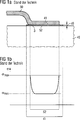
Ein Querschnitt durch eine typische Kontaktstelle gemäß dem Stand der Technik ist in
Das Anschlusselement
Wie aus
Aus der
Die
In der
Aus der
Die
Die
Aus der
Die
In der
Die
In der
Es ist die Aufgabe der vorliegenden Erfindung, ein Halbleiterbauelement mit einem Halbleiterkörper bereit zu stellen, dessen Anschlusselemente zuverlässig und temperaturwechselstabil mit einer Kontaktfläche des Halbleiterkörpers verbunden sind.It is the object of the present invention to provide a semiconductor component having a semiconductor body, the connection elements of which are reliably and temperature-stable connected to a contact surface of the semiconductor body.
Diese Aufgabe wird durch ein Halbleiterbauelement gemäß Anspruch 1 gelöst. Vorteilhafte Ausgestaltungen und Weiterbildungen der Erfindung sind Gegenstand von Unteransprüchen.This object is achieved by a semiconductor device according to
Ein erfindungsgemäßes Halbleiterbauelement weist einen Halbleiterkörper mit einer ersten Kontaktfläche sowie ein Anschlusselement mit einer zweiten Kontaktfläche auf. Das Anschlusselement ist als Bonddraht, als Anschlussclip oder als Leiterbahn ausgebildet. Die erste Kontaktfläche weist in einer horizontalen Richtung einen ersten Rand und die zweite Kontaktfläche in der horizontalen Richtung einen zweiten Rand auf.A semiconductor component according to the invention has a semiconductor body with a first contact surface and a connection element with a second contact surface. The connection element is designed as a bonding wire, as a connection clip or as a conductor track. The first contact surface has a first edge in a horizontal direction and the second contact surface has a second edge in the horizontal direction.
Die erste Kontaktfläche und die zweite Kontaktfläche sind in einer vertikalen Richtung voneinander beabstandet und mittels einer zwischen diesen angeordneten Ausgleichsmetallisierung zum Ausgleich thermomechanischer Spannungen mechanisch und elektrisch leitend verbunden. In der horizontalen Richtung ist die Ausgleichsmetallisierung vollständig innerhalb der horizontalen Begrenzungen der ersten Kontaktfläche angeordnet, oder der erste Rand fällt mit dem horizontalen Erstreckungsbereich der Ausgleichsmetallisierung zusammen. Jeder der Vertikalabschnitte ist in der horizontalen Richtung weiter vom ersten Rand beabstandet als jeder andere in der vertikalen Richtung näher an der ersten Kontaktfläche angeordnete Vertikalabschnitt.The first contact surface and the second contact surface are spaced apart in a vertical direction and mechanically and electrically connected by means of a compensation metallization arranged between them for compensation of thermo-mechanical stresses. In the horizontal direction, the balance metallization is disposed entirely within the horizontal boundaries of the first contact area, or the first edge coincides with the horizontal extension area of the balance metallization. Each of the vertical sections is spaced farther from the first edge in the horizontal direction than any other in the vertical direction closer to the first contact surface arranged vertical section.
Ein erster der Vertikalabschnitt, sowie ein zweiter der Vertikalabschnitte, der näher an der ersten Kontaktfläche angeordnet ist als der erste Vertikalabschnitt, weisen in der vertikalen Richtung jeweils eine Dicke von wenigstens 15 μm auf und sind aus Kupfer, einer Kupferlegierung, Aluminium, einer Aluminiumlegierung oder einer Kupfer-Aluminium-Legierung gebildet.A first of the vertical portion and a second one of the vertical portions located closer to the first contact surface than the first vertical portion have thicknesses of at least 15 μm each in the vertical direction and are made of copper, a copper alloy, aluminum, an aluminum alloy or a copper-aluminum alloy formed.
Außerdem weist die Ausgleichsmetallisierung eine Dicke von wenigstens 10 μm auf, sowie wenigstens zwei als Schichten ausgebildete Vertikalabschnitte, die in der vertikalen Richtung stufig aufeinanderfolgend angeordnet sind, wodurch ein Großteil der auftretenden thermomechanischen Spannungen innerhalb der Ausgleichsmetallisierung abgebaut wird. Zwischen zwei Vertikalabschnitten ist eine Stufe ausgebildet, deren Breite in der horizontalen Richtung wenigstens das Doppelte der Dicke des von den beiden Vertikalabschnitten näher an der ersten Kontaktfläche angeordneten Vertikalabschnittes beträgt.In addition, the compensation metallization has a thickness of at least 10 .mu.m, as well as at least two vertical sections formed as layers, which are arranged successively in the vertical direction successively, whereby a large part of the occurring thermo-mechanical stresses is reduced within the Ausgleichsmetallisierung. Between two vertical sections, a step is formed whose width in the horizontal direction is at least twice the thickness of the vertical section located closer to the first contact surface from the two vertical sections.
Während herkömmliche erste Verbindungsschichten lediglich dazu dienen, eine Kontaktierbarkeit des Halbleiterkörpers zu ermöglichen, ist eine Ausgleichsmetallisierung eines erfindungsgemäßen Halbleiterbauelements zum Ausgleich thermomechanischer Spannungen vorgesehen und weist daher eine erheblich größere Dicke auf. Je dicker eine solche Ausgleichsmetallisierung ausgebildet ist, desto geringer ist der Gradient der thermomechanischen Spannung, die im Bereich der Kontaktierung zwischen dem Halbleiterkörper und dem Anschlusselement abgebaut werden muss.While conventional first interconnection layers merely serve to allow contactability of the semiconductor body, compensating metallization of a semiconductor device according to the invention for compensating for thermomechanical stresses is provided and therefore has a considerably greater thickness. The thicker such a compensation metallization is formed, the lower the gradient of the thermo-mechanical stress which must be dissipated in the region of the contact between the semiconductor body and the connection element.
Bevorzugt weisen erste Verbindungsschichten Dicken zwischen 1 μm und 20 μm auf. Die Ausgleichsmetallisierung und die erste Verbindungsschicht können optional einstückig ausgebildet sein.Preferably, first connecting layers have thicknesses between 1 μm and 20 μm. The compensation metallization and the first connection layer can optionally be formed in one piece.
Die mechanische und elektrisch leitende Verbindung zwischen dem Anschlusselement und der Ausgleichsmetallisierung erfolgt im Bereich der zweiten Kontaktfläche. Dabei kann das Anschlusselement unmittelbar mit der Ausgleichsmetallisierung verbunden sein, wie dies z. B. beim Ultraschallbonden des Anschlusselementes der Fall ist.The mechanical and electrically conductive connection between the connection element and the compensation metallization takes place in the region of the second contact surface. In this case, the connection element can be connected directly to the Ausgleichsmetallisierung, as z. B. in the ultrasonic bonding of the connection element is the case.
Optional kann jedoch auch zusätzliches Material, beispielsweise ein Lot, verwendet werden, das zwischen der Ausgleichsmetallisierung und dem Anschlusselement angeordnet ist.Optionally, however, it is also possible to use additional material, for example a solder, which is arranged between the compensation metallization and the connection element.
Um die bei der Verbindung zwischen der ersten Kontaktfläche und dem Anschlusselement an den Rändern der zweite Kontaktfläche auftretenden maximalen thermomechanischen Spannung, wie diese anhand der
Bei der stufigen Ausgleichsmetallisierung ist vorzugsweise zumindest ein Vertikalabschnitt in der horizontalen Richtung weiter vom Rand der ersten Kontaktfläche beabstandet als jeder andere in der vertikalen Richtung näher an der ersten Kontaktfläche angeordnete Vertikalabschnitt.In the graded balance metallization, at least one vertical portion in the horizontal direction is preferably spaced farther from the edge of the first contact surface than any other vertical portion located closer to the first contact surface in the vertical direction.
Indem jeder der Vertikalabschnitte in der horizontalen Richtung weiter vom ersten Rand der ersten Kontaktfläche beabstandet ist als jeder andere in der vertikalen Richtung näher an der ersten Kontaktfläche angeordnete Vertikalabschnitt, wird erreicht, dass zwischen zwei beliebigen in der vertikalen Richtung benachbarten oder aneinander grenzenden Vertikalabschnitten jeweils eine Stufe ausgebildet ist.In that each of the vertical sections in the horizontal direction is spaced farther from the first edge of the first contact surface than any other vertical section arranged closer to the first contact surface in the vertical direction, it is achieved that one between each two vertically adjacent or adjacent vertical sections Stage is formed.
Gemäß einer bevorzugten Ausführungsform ist zumindest ein Vertikalabschnitt in allen seinen zur vertikalen Richtung senkrechten Schnittebenen in der horizontalen Richtung gleich weit vom Rand der ersten Kontaktfläche beabstandet. In gleicher Weise kann dies auch für mehrere oder für alle Vertikalabschnitte der Ausgleichsmetallisierung zutreffen, wobei verschiedene Vertikalabschnitte in der horizontalen Richtung vorzugsweise unterschiedlich weit vom Rand der ersten Kontaktfläche beabstandet sind.According to a preferred embodiment, at least one vertical section is equidistant from the edge of the first contact surface in all its sectional planes perpendicular to the vertical direction in the horizontal direction. In the same way, this may also apply to several or all vertical sections of the compensating metallization, wherein different vertical sections in the horizontal direction are preferably at different distances from the edge of the first contact surface.
Ein ausreichender Abbau der im Bereich der Kontaktstelle auftretenden thermomechanischen Spannungen wird dadurch erreicht, dass die in der horizontalen Richtung gemessene Breite einer Stufe wenigstens das Doppelte von deren Höhe, d. h. der Dicke des betreffenden Vertikalabschnitts, beträgt. Entsprechendes gilt gemäß einer bevorzugten Ausgestaltung auch für die Stufe, die zwischen der zweiten Kontaktfläche und dem von der ersten Kontaktfläche am weitesten beabstandeten Vertikalabschnitt ausgebildet ist.Sufficient degradation of the occurring in the region of the contact point thermo-mechanical stresses is achieved in that the measured width in the horizontal direction of a step at least twice their height, d. H. the thickness of the respective vertical section is. According to a preferred embodiment, the same also applies to the step which is formed between the second contact surface and the vertical section furthest from the first contact surface.
Die Erfindung wird nachfolgend in Ausführungsbeispielen anhand von Figuren näher erläutert. In den Figuren zeigen: The invention will be explained in more detail in exemplary embodiments with reference to figures. In the figures show:
In den Figuren bezeichnen gleiche Bezugszeichen gleiche Teile mit gleicher Bedeutung.In the figures, like reference numerals designate like parts with the same meaning.
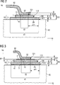
Infolge der stufigen Anordnung verteilen sich die aus
Die erste Kontaktfläche
Das Anschlusselement
Die Ausgleichsmetallisierung
Um eine möglichst gleichmäßige Verteilung der thermomechanischen Spannungen im Bereich der Stufenübergänge zu erhalten ist es vorteilhaft, wenn die Dicken d1, d2 der Vertikalabschnitte
Besonders gute Verhältnisse betreffend die Dauerhaftigkeit einer temperaturwechselfesten Verbindung zwischen der ersten Kontaktfläche
Im Unterschied zu der Kontaktstelle gemäß
Die Dicke d3 der ersten Verbindungsschicht
Der Aufbau der Ausgleichsmetallisierung
Entsprechend einer bevorzugten Ausführungsform der Erfindung ist auch zwischen der zweiten Verbindungsschicht
Ein weiteres bevorzugtes Ausführungsbeispiel eines erfindungsgemäßen Halbleiterbauelements ist in
Auf seiner dem Substrat
Zur elektrisch leitenden und mechanischen Verbindung des Halbleiterkörpers
Während die Ausgleichsmetallisierung
Die Ausgleichsmetallisierung
Zwischen der Ausgleichsmetallisierung
Das Verbindungsgefüge ausgehend von der ersten Kontaktfläche
Weiterhin kann auch an der Ausgleichsmetallisierung
Ist zwischen der Ausgleichsmetallisierung
Insgesamt umfasst das Verbindungsgefüge bei dem Ausführungsbeispiel gemäß
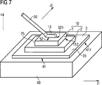
In der horizontalen Richtung r weist die erste Kontaktfläche
Die Ausgleichsmetallisierung
Die Ausgleichsmetallisierung
Die Vertikalabschnitte
Auf den Halbleiterkörper
Eine Isolierfolie
Das Anschlusselement
Ein als Leiterbahn ausgebildetes Anschlusselement
Die Ausgleichsmetallisierungen
Um eine ausreichend hohe Stromtragfähigkeit des Anschlusselements
Eine zu
Die anhand der
In den gezeigten Ausführungsbeispielen wurde der gestufte Aufbau eines Verbindungsgefüges ausgehend von einer Kontaktstelle über eine optionale erste Verbindungsschicht, eine Ausgleichsmetallisierung, eine optionale zweite Verbindungsschicht mit einem Anschlusselement in Bezug auf eine horizontale Richtung r bezogen. In entsprechender Weise kann der Aufbau des Verbindungsgefüges auch in einander entgegengesetzten horizontalen Richtungen r jeweils gestuft gewählt sein.In the exemplary embodiments shown, the stepped structure of a connection structure was based on a contact point via an optional first connection layer, a compensation metallization, an optional second connection layer with a connection element with respect to a horizontal direction r. In a corresponding manner, the structure of the connecting structure can also be selected in each case stepped in horizontal opposing directions r.
Wie in
Die Breiten aller vorhandenen Stufen, von denen in
BezugszeichenlisteLIST OF REFERENCE NUMBERS
- 11
- Vertikalabschnittvertical section
- 22
- Vertikalabschnittvertical section
- 33
- erste Verbindungsschichtfirst connection layer
- 44
- zweite Verbindungsschichtsecond connection layer
- 1010
- AusgleichsmetallisierungAusgleichsmetallisierung
- 1212
- dem Rand zugewandte Seite des ersten Vertikalabschnittesthe edge facing side of the first vertical section
- 1515
- Stufestep
- 2222
- dem Rand zugewandte Seite des zweiten Vertikalabschnittesthe edge facing side of the second vertical section
- 2525
- Stufestep
- 3131
- Kontaktierungsbereichcontacting
- 3535
- Stufestep
- 4040
- HalbleiterkörperSemiconductor body
- 4141
- erste Kontaktflächefirst contact surface
- 5050
- Anschlusselementconnecting element
- 50a–d50a-d
- Anschlusselemente (Leiterbahnen)Connection elements (conductors)
- 5151
- Passivierungpassivation
- 5252
- zweite Kontaktflächesecond contact surface
- 5454
- Metallmaskierungmetal mask
- 5555
- Isolierfolieinsulation
- 6060
- Substratsubstratum
- 6161
- Lotsolder
- 101101
- dem Rand der ersten Kontaktfläche zugewandte Seite der Metallisierungsschichtthe edge of the first contact surface facing side of the metallization
- 112112
- Rand des Übergangsbereichs zwischen dem ersten Vertikalabschnitt und dem zweiten VertikalabschnittEdge of the transition region between the first vertical portion and the second vertical portion
- 411411
- Rand der ersten KontaktflächeEdge of the first contact surface
- 521521
- dem Rand der ersten Kontaktfläche zugewandte Seite der ersten Grenzschichtthe edge of the first contact surface facing side of the first boundary layer
- d0d0
- Abstand der Schnittebene von der ersten KontaktflächeDistance of the cutting plane from the first contact surface
- d1d1
- Dicke des ersten VertikalabschnittesThickness of the first vertical section
- d2d2
- Dicke des zweiten VertikalabschnittesThickness of the second vertical section
- d3d3
- Dicke der ersten VerbindungsschichtThickness of the first tie layer
- d4d4
- Dicke der zweiten VerbindungsschichtThickness of the second bonding layer
- d10d10
- Dicke der AusgleichsmetallisierungThickness of the compensation metallization
- d501d501
- Minimale Dicke des Anschlusselementes innerhalb der ersten KontaktflächeMinimum thickness of the connection element within the first contact surface
- d502D502
- Dicke des Anschlusselementes außerhalb der ersten KontaktflächeThickness of the connection element outside the first contact surface
- Ee
- Schnittebenecutting plane
- rr
- horizontale Richtunghorizontal direction
- r1r1
- horizontale Richtunghorizontal direction
- r2r2
- horizontale Richtunghorizontal direction
- vv
- vertikale Richtungvertical direction
- x1x1
- horizontaler Abstand zwischen dem Rand der ersten Kontaktfläche und dem ersten Vertikalabschnitthorizontal distance between the edge of the first contact surface and the first vertical portion
- x2x2
- horizontaler Abstand zwischen dem Rand der ersten Kontaktfläche und dem zweiten Vertikalabschnitthorizontal distance between the edge of the first contact surface and the second vertical portion
- x52x52
- horizontaler Abstand zwischen dem Rand der ersten Kontaktfläche und dem Rand der zweiten Kontaktflächehorizontal distance between the edge of the first contact surface and the edge of the second contact surface
- xExE
- horizontaler Abstand zwischen der Ausgleichsmetallisierung und dem Rand der ersten Kontaktfläche in einer Schnittebene der Ausgleichsmetallisierung.Horizontal distance between the compensation metallization and the edge of the first contact surface in a sectional plane of the compensation metallization.
Claims (18)
Priority Applications (1)
| Application Number | Priority Date | Filing Date | Title |
|---|---|---|---|
| DE102004059389A DE102004059389B4 (en) | 2004-12-09 | 2004-12-09 | Semiconductor device with compensation metallization |
Applications Claiming Priority (1)
| Application Number | Priority Date | Filing Date | Title |
|---|---|---|---|
| DE102004059389A DE102004059389B4 (en) | 2004-12-09 | 2004-12-09 | Semiconductor device with compensation metallization |
Publications (2)
| Publication Number | Publication Date |
|---|---|
| DE102004059389A1 DE102004059389A1 (en) | 2006-06-14 |
| DE102004059389B4 true DE102004059389B4 (en) | 2012-02-23 |
Family
ID=36500172
Family Applications (1)
| Application Number | Title | Priority Date | Filing Date |
|---|---|---|---|
| DE102004059389A Expired - Fee Related DE102004059389B4 (en) | 2004-12-09 | 2004-12-09 | Semiconductor device with compensation metallization |
Country Status (1)
| Country | Link |
|---|---|
| DE (1) | DE102004059389B4 (en) |
Cited By (1)
| Publication number | Priority date | Publication date | Assignee | Title |
|---|---|---|---|---|
| US8823175B2 (en) | 2012-05-15 | 2014-09-02 | Infineon Technologies Ag | Reliable area joints for power semiconductors |
Families Citing this family (9)
| Publication number | Priority date | Publication date | Assignee | Title |
|---|---|---|---|---|
| US8164176B2 (en) * | 2006-10-20 | 2012-04-24 | Infineon Technologies Ag | Semiconductor module arrangement |
| DE102007023590A1 (en) * | 2007-05-21 | 2008-11-27 | Epcos Ag | Component with mechanically loadable connection surface |
| DE102009045181B4 (en) | 2009-09-30 | 2020-07-09 | Infineon Technologies Ag | Power semiconductor module |
| DE102015219183B4 (en) | 2015-10-05 | 2019-06-06 | Infineon Technologies Ag | Power semiconductor device, semiconductor module, method for processing a power semiconductor device |
| DE102016122318A1 (en) * | 2016-11-21 | 2018-05-24 | Infineon Technologies Ag | Connection structure of a power semiconductor device |
| US10304782B2 (en) | 2017-08-25 | 2019-05-28 | Infineon Technologies Ag | Compressive interlayer having a defined crack-stop edge extension |
| US11127693B2 (en) | 2017-08-25 | 2021-09-21 | Infineon Technologies Ag | Barrier for power metallization in semiconductor devices |
| US10734320B2 (en) | 2018-07-30 | 2020-08-04 | Infineon Technologies Austria Ag | Power metallization structure for semiconductor devices |
| US11031321B2 (en) | 2019-03-15 | 2021-06-08 | Infineon Technologies Ag | Semiconductor device having a die pad with a dam-like configuration |
Citations (16)
| Publication number | Priority date | Publication date | Assignee | Title |
|---|---|---|---|---|
| DE2204490A1 (en) * | 1972-01-31 | 1973-08-09 | Siemens Ag | SEMICONDUCTOR COMPONENT WITH PRESSURE CONTACT |
| US4258382A (en) * | 1978-07-03 | 1981-03-24 | National Semiconductor Corporation | Expanded pad structure |
| DE3888476D1 (en) * | 1987-12-08 | 1994-04-21 | Matsushita Electric Industrial Co Ltd | Electrical contact points and housings provided with them. |
| DE19612838A1 (en) * | 1995-11-13 | 1997-05-15 | Asea Brown Boveri | Power semiconductor component, e.g. thyristor, for high voltage direct current use |
| DE10003671A1 (en) * | 1999-01-28 | 2000-08-10 | Hitachi Ltd | Semiconductor component, especially a surface mountable semiconductor package, has front and back face electrodes connected to metal parts by precious metal-containing bodies or layers |
| US6159841A (en) * | 1994-12-30 | 2000-12-12 | Siliconix Incorporated | Method of fabricating lateral power MOSFET having metal strap layer to reduce distributed resistance |
| DE10048859A1 (en) * | 2000-10-02 | 2002-04-18 | Infineon Technologies Ag | Pressure contact arrangement, is designed for uniform pressure distribution when holding electronic component between contact surfaces |
| US20020084516A1 (en) * | 2000-10-27 | 2002-07-04 | Efland Taylor R. | Individualized low parasitic power distribution lines deposited over active integrated circuits |
| US20020149118A1 (en) * | 2001-03-06 | 2002-10-17 | Katsumi Yamaguchi | Semiconductor device and bump formation method |
| DE10134943A1 (en) * | 2001-07-23 | 2002-10-17 | Infineon Technologies Ag | Electronic power component comprises a semiconductor chip having contact surfaces of source contacts on its active surface and a gate contact |
| EP1259103A1 (en) * | 2000-02-25 | 2002-11-20 | Ibiden Co., Ltd. | Multilayer printed wiring board and method for producing multilayer printed wiring board |
| WO2003030247A2 (en) * | 2001-09-28 | 2003-04-10 | Siemens Aktiengesellschaft | Method for contacting electrical contact surfaces of a substrate and device consisting of a substrate having electrical contact surfaces |
| EP1353377A2 (en) * | 2002-04-12 | 2003-10-15 | NEC Compound Semiconductor Devices, Ltd. | Semiconductor device having pad electrode connected to wire |
| DE10343180A1 (en) * | 2003-09-18 | 2005-04-14 | Robert Bosch Gmbh | Method for producing a high-temperature-resistant gold wire connection |
| DE10355925A1 (en) * | 2003-11-29 | 2005-06-30 | Semikron Elektronik Gmbh | Power semiconductor module and method of its manufacture |
| DE102004036140A1 (en) * | 2004-07-26 | 2006-03-23 | Infineon Technologies Ag | Semiconductor device |
-
2004
- 2004-12-09 DE DE102004059389A patent/DE102004059389B4/en not_active Expired - Fee Related
Patent Citations (17)
| Publication number | Priority date | Publication date | Assignee | Title |
|---|---|---|---|---|
| DE2204490A1 (en) * | 1972-01-31 | 1973-08-09 | Siemens Ag | SEMICONDUCTOR COMPONENT WITH PRESSURE CONTACT |
| US4258382A (en) * | 1978-07-03 | 1981-03-24 | National Semiconductor Corporation | Expanded pad structure |
| DE3888476D1 (en) * | 1987-12-08 | 1994-04-21 | Matsushita Electric Industrial Co Ltd | Electrical contact points and housings provided with them. |
| DE3888476T2 (en) | 1987-12-08 | 1994-09-29 | Matsushita Electric Ind Co Ltd | Electrical contact points and housings provided with them. |
| US6159841A (en) * | 1994-12-30 | 2000-12-12 | Siliconix Incorporated | Method of fabricating lateral power MOSFET having metal strap layer to reduce distributed resistance |
| DE19612838A1 (en) * | 1995-11-13 | 1997-05-15 | Asea Brown Boveri | Power semiconductor component, e.g. thyristor, for high voltage direct current use |
| DE10003671A1 (en) * | 1999-01-28 | 2000-08-10 | Hitachi Ltd | Semiconductor component, especially a surface mountable semiconductor package, has front and back face electrodes connected to metal parts by precious metal-containing bodies or layers |
| EP1259103A1 (en) * | 2000-02-25 | 2002-11-20 | Ibiden Co., Ltd. | Multilayer printed wiring board and method for producing multilayer printed wiring board |
| DE10048859A1 (en) * | 2000-10-02 | 2002-04-18 | Infineon Technologies Ag | Pressure contact arrangement, is designed for uniform pressure distribution when holding electronic component between contact surfaces |
| US20020084516A1 (en) * | 2000-10-27 | 2002-07-04 | Efland Taylor R. | Individualized low parasitic power distribution lines deposited over active integrated circuits |
| US20020149118A1 (en) * | 2001-03-06 | 2002-10-17 | Katsumi Yamaguchi | Semiconductor device and bump formation method |
| DE10134943A1 (en) * | 2001-07-23 | 2002-10-17 | Infineon Technologies Ag | Electronic power component comprises a semiconductor chip having contact surfaces of source contacts on its active surface and a gate contact |
| WO2003030247A2 (en) * | 2001-09-28 | 2003-04-10 | Siemens Aktiengesellschaft | Method for contacting electrical contact surfaces of a substrate and device consisting of a substrate having electrical contact surfaces |
| EP1353377A2 (en) * | 2002-04-12 | 2003-10-15 | NEC Compound Semiconductor Devices, Ltd. | Semiconductor device having pad electrode connected to wire |
| DE10343180A1 (en) * | 2003-09-18 | 2005-04-14 | Robert Bosch Gmbh | Method for producing a high-temperature-resistant gold wire connection |
| DE10355925A1 (en) * | 2003-11-29 | 2005-06-30 | Semikron Elektronik Gmbh | Power semiconductor module and method of its manufacture |
| DE102004036140A1 (en) * | 2004-07-26 | 2006-03-23 | Infineon Technologies Ag | Semiconductor device |
Cited By (1)
| Publication number | Priority date | Publication date | Assignee | Title |
|---|---|---|---|---|
| US8823175B2 (en) | 2012-05-15 | 2014-09-02 | Infineon Technologies Ag | Reliable area joints for power semiconductors |
Also Published As
| Publication number | Publication date |
|---|---|
| DE102004059389A1 (en) | 2006-06-14 |
Similar Documents
| Publication | Publication Date | Title |
|---|---|---|
| DE102011083223B4 (en) | Power semiconductor module with integrated thick-film circuit board | |
| DE112006002516B4 (en) | Chip resistor and mounting structure for a chip resistor | |
| EP3262666B1 (en) | Electrical element and method for manufacturing it | |
| DE69500388T2 (en) | Film circuit metal system for use in IC components with bumps | |
| EP3599636B1 (en) | Ceramic circuit carrier and electronic unit | |
| DE102015205704B4 (en) | Contact arrangement and method for producing the contact arrangement | |
| DE102005028951B4 (en) | Arrangement for the electrical connection of a semiconductor circuit arrangement with an external contact device | |
| DE19811870B4 (en) | thermistor | |
| DE10033977A1 (en) | Intermediate coupling structure for mounting semiconductor chip on printed circuit board has conductor paths between contact pads and bonding pads on opposite sides of dielectric body | |
| DE102004059389B4 (en) | Semiconductor device with compensation metallization | |
| DE102005049687A1 (en) | Power semiconductor component in flat conductor technology with vertical current path | |
| DE102022130260A1 (en) | electrical module | |
| DE102004048688B4 (en) | Power semiconductor device | |
| DE69207507T2 (en) | PCB | |
| DE102008033410B4 (en) | Power electronic connection device with a power semiconductor component and manufacturing method for this purpose | |
| EP0152557A1 (en) | Semiconductor component having metallic bump contacts and multi-layer wiring | |
| DE112020001996T5 (en) | MOUNTING STRUCTURE FOR A CURRENT DETECTION RESISTOR AND A CURRENT DETECTION RESISTOR | |
| DE19830158C2 (en) | Intermediate carrier substrate with high wiring density for electronic components | |
| DE102004036905A1 (en) | Vertical power semiconductor device with a semiconductor chip and method for producing the same | |
| WO2008009347A1 (en) | Temperature sensor, and method for the production thereof | |
| EP3054480B1 (en) | Contact assembly and power module | |
| DE102007044046B4 (en) | Method for internal contacting of a power semiconductor module | |
| DE102007002807B4 (en) | chip system | |
| DE102015101571B4 (en) | WAFER-BASED BEOL PROCESS FOR CHIP EMBEDDING AND DEVICE | |
| DE102010000951B4 (en) | Power semiconductor module with reduced line resistance and method |
Legal Events
| Date | Code | Title | Description |
|---|---|---|---|
| OP8 | Request for examination as to paragraph 44 patent law | ||
| 8127 | New person/name/address of the applicant |
Owner name: INFINEON TECHNOLOGIES AG, 81669 MUENCHEN, DE |
|
| R016 | Response to examination communication | ||
| R018 | Grant decision by examination section/examining division | ||
| R082 | Change of representative |
Representative=s name: , |
|
| R020 | Patent grant now final |
Effective date: 20120524 |
|
| R119 | Application deemed withdrawn, or ip right lapsed, due to non-payment of renewal fee |