DE112006002516B4 - Chip resistor and mounting structure for a chip resistor - Google Patents
Chip resistor and mounting structure for a chip resistor Download PDFInfo
- Publication number
- DE112006002516B4 DE112006002516B4 DE112006002516.3T DE112006002516T DE112006002516B4 DE 112006002516 B4 DE112006002516 B4 DE 112006002516B4 DE 112006002516 T DE112006002516 T DE 112006002516T DE 112006002516 B4 DE112006002516 B4 DE 112006002516B4
- Authority
- DE
- Germany
- Prior art keywords
- electrode layers
- chip resistor
- resistance element
- pair
- ceramic substrate
- Prior art date
- Legal status (The legal status is an assumption and is not a legal conclusion. Google has not performed a legal analysis and makes no representation as to the accuracy of the status listed.)
- Active
Links
Images


Classifications
-
- H—ELECTRICITY
- H01—ELECTRIC ELEMENTS
- H01C—RESISTORS
- H01C1/00—Details
- H01C1/14—Terminals or tapping points specially adapted for resistors; Arrangements of terminals or tapping points on resistors
- H01C1/142—Terminals or tapping points specially adapted for resistors; Arrangements of terminals or tapping points on resistors the terminals or tapping points being coated on the resistive element
-
- H—ELECTRICITY
- H01—ELECTRIC ELEMENTS
- H01C—RESISTORS
- H01C1/00—Details
- H01C1/01—Mounting; Supporting
- H01C1/012—Mounting; Supporting the base extending along and imparting rigidity or reinforcement to the resistive element
-
- H—ELECTRICITY
- H01—ELECTRIC ELEMENTS
- H01C—RESISTORS
- H01C17/00—Apparatus or processes specially adapted for manufacturing resistors
- H01C17/006—Apparatus or processes specially adapted for manufacturing resistors adapted for manufacturing resistor chips
-
- H—ELECTRICITY
- H01—ELECTRIC ELEMENTS
- H01C—RESISTORS
- H01C7/00—Non-adjustable resistors formed as one or more layers or coatings; Non-adjustable resistors made from powdered conducting material or powdered semi-conducting material with or without insulating material
- H01C7/003—Thick film resistors
Landscapes
- Engineering & Computer Science (AREA)
- Microelectronics & Electronic Packaging (AREA)
- Manufacturing & Machinery (AREA)
- Physics & Mathematics (AREA)
- Electromagnetism (AREA)
- Non-Adjustable Resistors (AREA)
- Apparatuses And Processes For Manufacturing Resistors (AREA)
Abstract
Chip-Widerstand (10), der umfasst:ein Keramiksubstrat (11) in Form eines rechtwinkligen Parallelepipeds;ein Widerstandselement (12), das auf der Oberfläche des Keramiksubstrats (11) angeordnet, in einem Bereich innerhalb der Umfangsgrenze der Oberfläche positioniert und im Wesentlichen aus Kupfer hergestellt ist;ein Paar erster Elektrodenschichten (13), die in Bereichen positioniert sind, die einen Teil des Widerstandselements (12) abdecken;ein Paar zweiter Elektrodenschichten (14), die in Bereichen, die die ersten Elektrodenschichten (13) abdecken, positioniert sind,eine isolierende Schutzschicht (15), die so positioniert ist, dass sie das Widerstandselement (12), das zwischen den zweiten Elektrodenschichten (14) freiliegt, abdeckt;ein Paar Stirnflächenelektroden (17), die an beiden longitudinalen Stirnflächen des Keramiksubstrats (11) positioniert sind, wobei das eine Ende an den zweiten Elektrodenschichten (14) eng anliegend befestigt ist; undeine Plattierungsschicht (18-21), die die zweiten Elektrodenschichten (14) und die Stirnflächenelektroden (17) abdeckt;wobei das Paar erster Elektrodenschichten (13) in Bereichen positioniert sind, die beide longitudinalen Stirnflächen des Widerstandselements (12) und die Oberfläche der longitudinalen Enden des Widerstandselements (12) von der Umfangsgrenze der Oberfläche des Keramiksubstrats (11) abdecken.A chip resistor (10) comprising: a ceramic substrate (11) in the shape of a right-angled parallelepiped; a resistor element (12) disposed on the surface of the ceramic substrate (11), positioned in an area within the peripheral boundary of the surface and substantially is made of copper; a pair of first electrode layers (13) positioned in areas covering a part of the resistance element (12); a pair of second electrode layers (14) positioned in areas covering the first electrode layers (13), an insulating protective layer (15) positioned so as to cover the resistance element (12) exposed between the second electrode layers (14); a pair of end-face electrodes (17) attached to both longitudinal end faces of the ceramic substrate ( 11) are positioned with one end closely attached to the second electrode layers (14); anda plating layer (18-21) covering the second electrode layers (14) and the end face electrodes (17); wherein the pair of first electrode layers (13) are positioned in areas both of the longitudinal end faces of the resistance element (12) and the surface of the longitudinal Cover ends of the resistance element (12) from the peripheral boundary of the surface of the ceramic substrate (11).
Description
TECHNISCHES GEBIETTECHNICAL AREA
Die vorliegende Erfindung bezieht sich auf einen Chip-Widerstand und insbesondere auf einen niederohmigen Chip-Widerstand, der z. B. zur Stromdetektion in einer elektronischen Schaltung verwendet wird. Ferner bezieht sich die Erfindung auf eine Befestigungsstruktur für einen Chip-Widerstand.The present invention relates to a chip resistor and more particularly to a low-ohmic chip resistor, e.g. B. is used for current detection in an electronic circuit. The invention also relates to a mounting structure for a chip resistor.
STAND DER TECHNIKSTATE OF THE ART
Chip-Widerstände sind in der Weise aufgebaut, dass ein Widerstandselement, das z. B. aus Rutheniumoxid hergestellt ist, zwischen einem Paar Elektrodenabschnitten angeordnet ist. Ein Chip-Widerstand, der z. B. für die Stromdetektion einer elektronischen Schaltung verwendet wird, muss jedoch einen Widerstandswert besitzen, der nicht größer als 1 Ω; ist. Eine Technologie, die ein im Wesentlichen aus Kupfer hergestelltes Widerstandselement verwendet, um einen derartigen niederohmigen Chip-Widerstand zu erhalten, ist seit langem bekannt (siehe z. B. das Patentdokument 1).Chip resistors are constructed in such a way that a resistance element, e.g. B. made of ruthenium oxide, is disposed between a pair of electrode sections. A chip resistor which z. B. is used for the current detection of an electronic circuit, but must have a resistance value that is not greater than 1 Ω; is. A technology using a resistance element made essentially of copper to obtain such a low-resistance chip resistor has long been known (see, for example, Patent Document 1).
Wenn der Chip-Widerstand 1, der in der oben beschriebenen Weise konfiguriert ist, auf einer Leiterplatte
Patentdokument 1: Japanische Offenlegungsschrift
Die
OFFENBARUNG DER ERFINDUNGDISCLOSURE OF THE INVENTION
PROBLEM, DAS DURCH DIE ERFINDUNG GELÖST WERDEN SOLLPROBLEM TO BE SOLVED BY THE INVENTION
Wie oben beschrieben wurde, kann ein niederohmiger Chip-Widerstand mit einem niedrigen TCR erhalten werden, wenn das Widerstandselement im Wesentlichen aus einer Kupfer-Nickel-Legierung hergestellt ist. Wenn der in
Dieser Typ des Chip-Widerstands wird hergestellt, indem ein großflächiges Mehrchipsubstrat einer primären Teilung unterzogen wird, um streifenförmige Substrate zu erhalten, und die streifenförmigen Substrate anschließend einer sekundären Teilung unterzogen werden, um einzelne Stücke zu erhalten. Bei dem oben erwähnten Chip-Widerstand 1 ist jedoch das Widerstandselement 3, das im Wesentlichen aus einer Kupfer-Nickel-Legierung hergestellt ist, über eine primäre Teilungsbrechkerbe in dem großflächigen Substrathinweg gebildet. Deswegen ist die Tätigkeit, die ausgeführt wird, um das großflächige Substrat längs der Brechkerbe in Streifen zu unterteilen, schwierig. Demzufolge wird die Fertigungsausbeute nachteilig beeinflusst.This type of chip resistor is manufactured by subjecting a large area multi-chip substrate to primary division to obtain strip-shaped substrates and then subjecting the strip-shaped substrates to secondary division to obtain individual pieces. In the above-mentioned chip resistor 1 however, the
Die vorliegende Erfindung wurde im Hinblick auf die oben beschriebene herkömmliche Technologie gemacht. Es ist eine Aufgabe der vorliegenden Erfindung, einen Chip-Widerstand zu schaffen, dessen elektrischer Widerstand leicht verringert werden kann und der eine ausgezeichnete Fertigungsausbeute aufweist.The present invention has been made in view of the conventional technology described above. It is an object of the present invention to provide a chip resistor whose electrical resistance can be easily reduced and which is excellent in manufacturing yield.
MITTEL ZUM LÖSEN DES PROBLEMSMEANS TO SOLVE THE PROBLEM
Die Erfindung ist in den Ansprüchen 1 und 3 definiert. Anspruch 2 beschreibt eine vorteilhafte Ausführungsform.The invention is defined in
Ferner ist ein Chip-Widerstandgemäß einem ersten Aspekt offenbart, der Folgendes umfasst: ein Keramiksubstrat in Form eines rechtwinkligen Parallelepipeds; ein Widerstandselement, das an der unteren Oberfläche des Keramiksubstrats angeordnet und in einem Bereich innerhalb der Umfangsgrenze der unteren Oberfläche positioniert und im Wesentlichen aus Kupfer hergestellt ist; ein Paar erster Elektrodenschichten, die in Bereichen positioniert sind, die beide longitudinalen Enden des Widerstandselements überdecken, ein Paar zweiter Elektrodenschichten, die in Bereichen positioniert sind, die die ersten Elektrodenschichten überdecken; eine isolierende Schutzschicht, die so positioniert ist, dass sie das Widerstandselement überdeckt, das zwischen den zweiten Elektrodenschichten freiliegt; ein Paar Stirnflächenelektroden, die an beiden longitudinalen Stirnflächen des Keramiksub-strats positioniert sind, wobei das untere Ende an den zweiten Elektrodenschich-ten eng anliegend befestigt ist; und eine Plattierungsschicht, die die zweiten Elektrodenschichten und die Stirnflächenelektroden überdeckt, wobei die Plattierungsschicht an ein Leitungsmuster auf einer Leiterplatte gelötet ist, wobei die ersten und die zweiten Elektrodenschichten auf dem Leitungsmuster positioniert sind, um den Chip-Widerstand auf der Leiterplatte zu montieren.Also disclosed is a chip resistor according to a first aspect, comprising: a ceramic substrate in the shape of a rectangular parallelepiped; a resistance element disposed on the lower surface of the ceramic substrate and positioned in an area within the peripheral boundary of the lower surface and made essentially of copper; a pair of first electrode layers positioned in areas overlapping both longitudinal ends of the resistance element; a pair of second electrode layers positioned in areas overlapping the first electrode layers; a protective insulating layer positioned so as to cover the resistance element exposed between the second electrode layers; a pair of end face electrodes positioned on both longitudinal end faces of the ceramic substrate, the lower end being closely attached to the second electrode layers; and a plating layer covering the second electrode layers and the end face electrodes, the plating layer being soldered to a wiring pattern on a circuit board, the first and second electrode layers being positioned on the wiring pattern to mount the chip resistor on the circuit board.
Der Chip-Widerstand, der in der oben beschriebenen Weise konfiguriert ist, besitzt ein Widerstandselement, das aus einem niederohmigen Werkstoff mit niedrigem TCR-Wert hergestellt ist. Wenn er mit der Vorderseite nach unten montiert ist, d. h. so montiert, dass die Seite des Widerstandselements der Komponentenseite der Leiterplatte zugewandt ist, kann er des Weiteren Energie zu dem Widerstandselement verteilen, wobei die Stirnflächenelektroden umgangen werden. Der Elektrodenabschnitt des Widerstandselements enthält ferner zwei Schichten, d. h. die ersten und die zweiten Elektrodenschichten, um einer vergrößerte Lagendicke zu schaffen. Deswegen kann für den Elektrodenabschnitt eine äußerst kleine Induktivitätseinstellung verwendet werden. Demzufolge können bei dem Chip-Widerstand sein elektrischer Widerstand leicht verringert und die TCR-Charakteristik verbessert werden. Außerdem ist das Widerstandselement an der unteren Oberfläche des Keramiksubstrats angeordnet und in einem Bereich innerhalb der Umfangsgrenze der unteren Oberfläche positioniert. Deswegen tritt das Widerstandselement während der Herstellung des Chip-Widerstands nicht in die Teilungsbrechkerbe in dem großflächigen Substrat ein. Dadurch kann eine Tätigkeit der primären Teilung gleichmäßig ausgeführt werden und es kann eine ausgezeichnete Fertigungsausbeute erzielt werden. Obwohl die Stirnflächenelektroden des Chip-Widerstands keine elektrische Verteilung darstellen, erzeugen sie eine Lötmittelkehle, wenn sie auf dem Leitungsmuster der Leiterplatte montiert und daran angelötet werden. Deswegen verstärken die Stirnflächenelektroden die Montagefestigkeit, die nach dem Montieren vorherrscht, beträchtlich.The chip resistor configured as described above has a resistance element made of a low-resistance material having a low TCR value. When mounted face down, i. H. mounted so that the side of the resistor element faces the component side of the circuit board, it can further distribute energy to the resistor element, bypassing the face electrodes. The electrode portion of the resistance element further includes two layers, i.e. H. the first and second electrode layers to provide increased sheet thickness. Therefore, an extremely small inductance setting can be used for the electrode portion. As a result, the chip resistor can easily reduce its electrical resistance and improve the TCR characteristic. In addition, the resistance element is disposed on the lower surface of the ceramic substrate and positioned in an area within the peripheral boundary of the lower surface. Because of this, the resistor element does not enter the division breaking notch in the large-area substrate during manufacture of the chip resistor. Thereby, a primary division operation can be performed smoothly and an excellent manufacturing yield can be obtained. Although the face electrodes of the chip resistor are not an electrical distribution, they create a solder fillet when they are mounted and soldered onto the circuit board wiring pattern. Therefore, the end face electrodes considerably strengthen the mounting strength that prevails after mounting.
Ferner ist ein Chip-Widerstandgemäß einem zweiten Aspekt offenbart, der in dem oben genannten Aspekt beschrieben ist, wobei die ersten und die zweiten Elektrodenschichten die gleiche Form haben und überlappen. In diesem Fall verringern sich die Anlagekosten, da die Elektrodenschichten unter Verwendung der gleichen Ausrüstung gebildet werden können.Also disclosed is a chip resistor according to a second aspect described in the above aspect, wherein the first and second electrode layers have the same shape and overlap. In this case, since the electrode layers can be formed using the same equipment, the equipment cost is reduced.
WIRKUNGEN DER ERFINDUNGEFFECTS OF THE INVENTION
Der Chip-Widerstand gemäß der vorliegenden Erfindung enthält ein Widerstandselement, das aus einem niederohmigen Werkstoff mit niedrigem TCR-Wert hergestellt ist. Wenn er mit der Vorderseite nach unten montiert ist, kann er des Weiteren Energie an das Widerstandselement verteilen, wobei die Stirnflächenelektroden umgangen werden. Der Elektrodenabschnitt des Widerstandselements enthält ferner zwei Schichten, d. h. die ersten und die zweiten Elektrodenschichten, und ermöglicht die Verwendung einer äußerst kleinen Induktivitätseinstellung. Demzufolge können bei dem Chip-Widerstand sein elektrischer Widerstand leicht verringert und die TCR Charakteristik verbessert werden. Außerdem tritt das Widerstandselement während der Herstellung des Chip-Widerstands nicht in die Teilungsbrechkerbe in dem großflächigen Substrat ein. Selbst dann, wenn das Widerstandselement aus einem sehr elastischen Werkstoff, der Kupfer enthält, hergestellt ist, erzeugt der Chip-Widerstand keine Grate. Demzufolge kann die Tätigkeit der primären Unterteilung gleichmäßig ausgeführt werden, um eine ausgezeichnete Fertigungsausbeute zu erreichen. Wenn der Chip-Widerstand auf einer Leiterplatte montiert ist, erzeugen die Stirnflächenelektroden eine Lötmittelkehle. Das erleichtert das Erreichen einer geforderten Montagefestigkeit.The chip resistor according to the present invention includes a resistance element made of a low-resistance material with a low TCR value. Further, when mounted face down, it can distribute energy to the resistive element, bypassing the face electrodes. The electrode portion of the resistance element further includes two layers, ie, the first and second electrode layers, and enables an extremely small inductance setting to be used. As a result, the chip resistor can easily reduce its electrical resistance and improve the TCR characteristic. In addition, the resistor element does not enter the division breaking notch in the large-area substrate during manufacture of the chip resistor. Even if the resistor element is made of a very elastic material containing copper, the chip resistor does not generate any burrs. As a result, the work of the primary dividing can be smoothly performed to provide a to achieve excellent manufacturing yield. When the chip resistor is mounted on a circuit board, the face electrodes create a solder fillet. This makes it easier to achieve the required assembly strength.
BESTE ART DER AUSFÜHRUNG DER ERFINDUNGBEST MODE FOR CARRYING OUT THE INVENTION
Im Folgenden werden Ausführungsformen der vorliegenden Erfindung unter Bezugnahme auf die beigefügte Zeichnung beschrieben.
Der Chip-Widerstand
Das Keramiksubstrat
Der Fertigungsprozess für den Chip-Widerstand
Zuerst wird eine leitende Paste auf Kupferbasis (oder Silberbasis) auf eine Oberfläche eines großflächigen Mehrchipsubstrats (die obere Oberfläche des Keramiksubstrats
Anschließend wird eine leitende Paste auf Kupferbasis (oder Silberbasis) auf einen Bereich, der beide longitudinale Enden jedes Widerstandselements
Wie in den
Anschließend wird das großflächige Substrat längs einer primären Teilungsbrechkerbe in Streifen geteilt. Nickelchrom wird dann durch Sputtern auf die freiliegenden Teilungsoberflächen jedes Substratstreifens aufgebracht, um Stirnflächenelektroden
Anschließend werden die Substratstreifen längs einer sekundären Teilungsbrechkerbe in einzelne Stücke geteilt. Die einzelnen Stücke werden dann nacheinander einer elektrolytischen Plattierung unterzogen, um die vier Plattierungsschichten
Der Chip-Widerstand
Wie oben beschrieben wurde, enthält der Chip-Widerstand
Außerdem ist das Widerstandselement
FigurenlisteFigure list
-
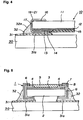
1 ist eine schematische Schnittansicht, die einen Chip-Widerstand gemäß einer Ausführungsform der vorliegenden Erfindung veranschaulicht;1 Fig. 13 is a schematic sectional view illustrating a chip resistor according to an embodiment of the present invention; -
2 sind Schnittansichten, die einen Fertigungsprozess für den Chip-Widerstand darstellen;2 Fig. 13 are sectional views showing a manufacturing process for the chip resistor; -
3 sind Draufsichten, die einen Fertigungsprozess für den Chip-Widerstand darstellen;3 Fig. 13 are plan views showing a manufacturing process for the chip resistor; -
4 ist eine Schnittansicht, die einen wesentlichen Teil des Chip-Widerstands, der auf einer Leiterplatte montiert ist, veranschaulicht und4th Fig. 13 is a sectional view illustrating an essential part of the chip resistor mounted on a circuit board and -
5 ist eine schematische Schnittansicht, die einen betreffenden niederohmigen Chip-Widerstand veranschaulicht.5 Fig. 13 is a schematic sectional view illustrating a related chip low-resistance resistor.
BezugszeichenlisteList of reference symbols
- 10:10:
- Chip-WiderstandChip resistance
- 11:11:
- KeramiksubstratCeramic substrate
- 12:12:
- WiderstandselementResistance element
- 12a:12a:
- AbrichtkerbeDressing notch
- 13:13:
- erste Elektrodenschichtfirst electrode layer
- 14:14:
- zweite Elektrodenschichtsecond electrode layer
- 15:15:
- SchutzschichtProtective layer
- 16:16:
- obere Elektrodeupper electrode
- 17:17:
- StirnflächenelektrodeFace electrode
- 18-21:18-21:
- PlattierungsschichtPlating layer
- 22:22:
- MarkierungsschichtMarking layer
- 30:30:
- LeiterplatteCircuit board
- 31:31:
- LeitungsmusterLine pattern
- 31a:31a:
- LötinselSoldering island
- 32:32:
- Lötmittelsolder
- 32a:32a:
- LötmittelkehleSolder fillet
Claims (3)
Applications Claiming Priority (3)
| Application Number | Priority Date | Filing Date | Title |
|---|---|---|---|
| JP2005-274231 | 2005-09-21 | ||
| JP2005274231A JP4841914B2 (en) | 2005-09-21 | 2005-09-21 | Chip resistor |
| PCT/JP2006/318737 WO2007034874A1 (en) | 2005-09-21 | 2006-09-21 | Chip resistor |
Publications (2)
| Publication Number | Publication Date |
|---|---|
| DE112006002516T5 DE112006002516T5 (en) | 2008-08-21 |
| DE112006002516B4 true DE112006002516B4 (en) | 2021-12-09 |
Family
ID=37888917
Family Applications (1)
| Application Number | Title | Priority Date | Filing Date |
|---|---|---|---|
| DE112006002516.3T Active DE112006002516B4 (en) | 2005-09-21 | 2006-09-21 | Chip resistor and mounting structure for a chip resistor |
Country Status (5)
| Country | Link |
|---|---|
| US (1) | US7782173B2 (en) |
| JP (1) | JP4841914B2 (en) |
| CN (1) | CN101268526B (en) |
| DE (1) | DE112006002516B4 (en) |
| WO (1) | WO2007034874A1 (en) |
Families Citing this family (38)
| Publication number | Priority date | Publication date | Assignee | Title |
|---|---|---|---|---|
| US7982582B2 (en) | 2007-03-01 | 2011-07-19 | Vishay Intertechnology Inc. | Sulfuration resistant chip resistor and method for making same |
| JP5225598B2 (en) * | 2007-03-19 | 2013-07-03 | コーア株式会社 | Electronic component and its manufacturing method |
| JP2010161135A (en) * | 2009-01-07 | 2010-07-22 | Rohm Co Ltd | Chip resistor, and method of making the same |
| US8389872B2 (en) * | 2009-07-29 | 2013-03-05 | Hermes-Epitek Corp. | Electrode structure adapted for high applied voltage and fabrication method thereof |
| US8284016B2 (en) | 2009-09-04 | 2012-10-09 | Samsung Electro-Mechanics Co., Ltd. | Array type chip resistor |
| TW201133517A (en) * | 2010-03-23 | 2011-10-01 | Yageo Corp | Chip resistor having a low resistance and method for manufacturing the same |
| JP5838373B2 (en) * | 2010-09-27 | 2016-01-06 | パナソニックIpマネジメント株式会社 | Discharge electrode manufacturing method, electrostatic atomizer, and ion generator |
| JP5360330B2 (en) * | 2011-02-24 | 2013-12-04 | パナソニック株式会社 | Chip resistor and manufacturing method thereof |
| JP2013074044A (en) * | 2011-09-27 | 2013-04-22 | Koa Corp | Chip resistor |
| JP2013153129A (en) | 2011-09-29 | 2013-08-08 | Rohm Co Ltd | Chip resistor and electronic equipment having resistor network |
| KR101892750B1 (en) * | 2011-12-19 | 2018-08-29 | 삼성전기주식회사 | chip resistor and fabricating method thereof |
| JP6134507B2 (en) * | 2011-12-28 | 2017-05-24 | ローム株式会社 | Chip resistor and manufacturing method thereof |
| JP2013153130A (en) * | 2011-12-28 | 2013-08-08 | Rohm Co Ltd | Chip resistor |
| JP2013232620A (en) | 2012-01-27 | 2013-11-14 | Rohm Co Ltd | Chip component |
| DE112012005984T5 (en) * | 2012-03-05 | 2014-12-04 | Mitsubishi Electric Corporation | Semiconductor device |
| KR101412951B1 (en) * | 2012-08-17 | 2014-06-26 | 삼성전기주식회사 | Resistor and method for manufacturing the same |
| JP6274789B2 (en) * | 2013-08-30 | 2018-02-07 | ローム株式会社 | Chip resistor |
| WO2016047259A1 (en) * | 2014-09-25 | 2016-03-31 | Koa株式会社 | Chip resistor and method for producing same |
| US9818512B2 (en) * | 2014-12-08 | 2017-11-14 | Vishay Dale Electronics, Llc | Thermally sprayed thin film resistor and method of making |
| US9997281B2 (en) | 2015-02-19 | 2018-06-12 | Rohm Co., Ltd. | Chip resistor and method for manufacturing the same |
| JP2016192509A (en) * | 2015-03-31 | 2016-11-10 | Koa株式会社 | Chip resistor |
| JP6495724B2 (en) * | 2015-04-15 | 2019-04-03 | Koa株式会社 | Chip resistor and manufacturing method thereof |
| JP6499007B2 (en) * | 2015-05-11 | 2019-04-10 | Koa株式会社 | Chip resistor |
| TWI616903B (en) * | 2015-07-17 | 2018-03-01 | 乾坤科技股份有限公司 | Micro-resistor |
| JP2017069441A (en) * | 2015-09-30 | 2017-04-06 | Koa株式会社 | Chip resistor |
| US10083781B2 (en) | 2015-10-30 | 2018-09-25 | Vishay Dale Electronics, Llc | Surface mount resistors and methods of manufacturing same |
| KR101883040B1 (en) * | 2016-01-08 | 2018-07-27 | 삼성전기주식회사 | Chip resistor |
| JP2017168817A (en) * | 2016-03-15 | 2017-09-21 | ローム株式会社 | Chip resistor and manufacturing method for the same |
| WO2018061961A1 (en) * | 2016-09-27 | 2018-04-05 | パナソニックIpマネジメント株式会社 | Chip resistor |
| JP7385358B2 (en) * | 2016-12-27 | 2023-11-22 | ローム株式会社 | chip resistor |
| US9928947B1 (en) * | 2017-07-19 | 2018-03-27 | National Cheng Kung University | Method of fabricating highly conductive low-ohmic chip resistor having electrodes of base metal or base-metal alloy |
| JPWO2019017237A1 (en) * | 2017-07-19 | 2020-05-28 | パナソニックIpマネジメント株式会社 | Chip resistor |
| US10438729B2 (en) * | 2017-11-10 | 2019-10-08 | Vishay Dale Electronics, Llc | Resistor with upper surface heat dissipation |
| DE102018101419A1 (en) * | 2018-01-23 | 2019-07-25 | Biotronik Se & Co. Kg | Electrical resistance, in particular for medical implants |
| US12068094B2 (en) | 2019-09-04 | 2024-08-20 | Semitec Corporation | Resistor unit, manufacturing method therefor, and device provided with resistor unit |
| JPWO2021095535A1 (en) * | 2019-11-12 | 2021-05-20 | ||
| TW202234615A (en) * | 2021-02-23 | 2022-09-01 | 旺詮股份有限公司 | High power chip resistor including a resistor body and two electrodes |
| KR20230121405A (en) * | 2022-02-11 | 2023-08-18 | 삼성전기주식회사 | Resistor Component |
Citations (2)
| Publication number | Priority date | Publication date | Assignee | Title |
|---|---|---|---|---|
| JPH10144501A (en) | 1996-09-11 | 1998-05-29 | Matsushita Electric Ind Co Ltd | Chip resistor and method of manufacturing the same |
| US6153256A (en) | 1998-08-18 | 2000-11-28 | Rohm Co., Ltd. | Chip resistor and method of making the same |
Family Cites Families (10)
| Publication number | Priority date | Publication date | Assignee | Title |
|---|---|---|---|---|
| US4829553A (en) * | 1988-01-19 | 1989-05-09 | Matsushita Electric Industrial Co., Ltd. | Chip type component |
| US5907274A (en) * | 1996-09-11 | 1999-05-25 | Matsushita Electric Industrial Co., Ltd. | Chip resistor |
| JP2000036401A (en) * | 1998-07-21 | 2000-02-02 | Murata Mfg Co Ltd | Resistive element and manufacture thereof |
| JP2000164402A (en) * | 1998-11-27 | 2000-06-16 | Rohm Co Ltd | Structure of chip resistor |
| JP2002353001A (en) * | 2001-05-25 | 2002-12-06 | Tateyama Kagaku Kogyo Kk | Thick film chip resistor |
| WO2003046934A1 (en) * | 2001-11-28 | 2003-06-05 | Rohm Co.,Ltd. | Chip resistor and method for producing the same |
| JP4046178B2 (en) * | 2002-03-25 | 2008-02-13 | コーア株式会社 | Chip resistor and manufacturing method thereof |
| JP3834251B2 (en) * | 2002-03-26 | 2006-10-18 | コーア株式会社 | Chip resistor and manufacturing method thereof |
| JP2004259864A (en) * | 2003-02-25 | 2004-09-16 | Rohm Co Ltd | Chip resistor |
| JP4295035B2 (en) * | 2003-08-06 | 2009-07-15 | 太陽社電気株式会社 | Manufacturing method of chip resistor |
-
2005
- 2005-09-21 JP JP2005274231A patent/JP4841914B2/en not_active Expired - Lifetime
-
2006
- 2006-09-21 CN CN2006800347684A patent/CN101268526B/en active Active
- 2006-09-21 WO PCT/JP2006/318737 patent/WO2007034874A1/en not_active Ceased
- 2006-09-21 DE DE112006002516.3T patent/DE112006002516B4/en active Active
- 2006-09-21 US US12/066,846 patent/US7782173B2/en active Active
Patent Citations (2)
| Publication number | Priority date | Publication date | Assignee | Title |
|---|---|---|---|---|
| JPH10144501A (en) | 1996-09-11 | 1998-05-29 | Matsushita Electric Ind Co Ltd | Chip resistor and method of manufacturing the same |
| US6153256A (en) | 1998-08-18 | 2000-11-28 | Rohm Co., Ltd. | Chip resistor and method of making the same |
Also Published As
| Publication number | Publication date |
|---|---|
| US7782173B2 (en) | 2010-08-24 |
| US20090108986A1 (en) | 2009-04-30 |
| CN101268526B (en) | 2012-08-15 |
| JP4841914B2 (en) | 2011-12-21 |
| WO2007034874A1 (en) | 2007-03-29 |
| DE112006002516T5 (en) | 2008-08-21 |
| JP2007088162A (en) | 2007-04-05 |
| CN101268526A (en) | 2008-09-17 |
Similar Documents
| Publication | Publication Date | Title |
|---|---|---|
| DE112006002516B4 (en) | Chip resistor and mounting structure for a chip resistor | |
| DE4339551C1 (en) | Resistor, constructed as a surface-mounted device, and method for its production, as well as a printed circuit board having such a resistor | |
| DE69902599T2 (en) | Resistance and its manufacturing process | |
| DE69512519T2 (en) | SURFACE MOUNTED LOCKING DEVICE | |
| DE112006002517T5 (en) | Chip Resistor | |
| DE69526971T2 (en) | IMPROVEMENTS TO CERAMIC CHIP FUSES | |
| DE2810054C2 (en) | Electronic circuit arrangement and method for its manufacture | |
| DE3705279C2 (en) | Process for manufacturing resistors in chip form | |
| DE69005785T2 (en) | Chip-type electrical resistance for surface mounting and process for its manufacture. | |
| DE69715091T2 (en) | Surface mount resistor | |
| DE2247902A1 (en) | Printed circuit board and process for making same | |
| DE19811870B4 (en) | thermistor | |
| DE4036109A1 (en) | RESISTANCE TEMPERATURE SENSOR | |
| DE69704678T2 (en) | METHOD FOR PRODUCING A TIN / LEAD LAYER PCB ASSEMBLY | |
| DE112016002156T5 (en) | Chip Resistor | |
| EP0841668B1 (en) | Electrical resistor and method of manufacturing the same | |
| DE69118308T2 (en) | Method of making an electrical connection for an integrated circuit | |
| DE112013001486T5 (en) | CHIP RESISTANT FOR EMBEDDING INTO A PCB AND METHOD FOR THE PRODUCTION THEREOF | |
| DE2916329A1 (en) | ELECTRICAL NETWORK | |
| DE112020001355T5 (en) | CHIP RESISTOR | |
| EP0234487B1 (en) | Thin film circuit and method for manufacturing the same | |
| DE3118342C2 (en) | Thermal recording head and method for its manufacture | |
| EP0484756B1 (en) | SMD-type resistor arrangement | |
| DE4036079A1 (en) | ELECTRONIC COMPONENT AND ELECTRONIC DEVICE WITH SUCH A COMPONENT | |
| DE3731969C2 (en) |
Legal Events
| Date | Code | Title | Description |
|---|---|---|---|
| R012 | Request for examination validly filed |
Effective date: 20130718 |
|
| R016 | Response to examination communication | ||
| R018 | Grant decision by examination section/examining division | ||
| R020 | Patent grant now final |