DE102004036140A1 - Semiconductor device - Google Patents
Semiconductor device Download PDFInfo
- Publication number
- DE102004036140A1 DE102004036140A1 DE102004036140A DE102004036140A DE102004036140A1 DE 102004036140 A1 DE102004036140 A1 DE 102004036140A1 DE 102004036140 A DE102004036140 A DE 102004036140A DE 102004036140 A DE102004036140 A DE 102004036140A DE 102004036140 A1 DE102004036140 A1 DE 102004036140A1
- Authority
- DE
- Germany
- Prior art keywords
- metallization
- semiconductor component
- component according
- layers
- dielectric
- Prior art date
- Legal status (The legal status is an assumption and is not a legal conclusion. Google has not performed a legal analysis and makes no representation as to the accuracy of the status listed.)
- Withdrawn
Links
Classifications
-
- H—ELECTRICITY
- H10—SEMICONDUCTOR DEVICES; ELECTRIC SOLID-STATE DEVICES NOT OTHERWISE PROVIDED FOR
- H10W—GENERIC PACKAGES, INTERCONNECTIONS, CONNECTORS OR OTHER CONSTRUCTIONAL DETAILS OF DEVICES COVERED BY CLASS H10
- H10W20/00—Interconnections in chips, wafers or substrates
- H10W20/01—Manufacture or treatment
- H10W20/031—Manufacture or treatment of conductive parts of the interconnections
-
- H—ELECTRICITY
- H10—SEMICONDUCTOR DEVICES; ELECTRIC SOLID-STATE DEVICES NOT OTHERWISE PROVIDED FOR
- H10W—GENERIC PACKAGES, INTERCONNECTIONS, CONNECTORS OR OTHER CONSTRUCTIONAL DETAILS OF DEVICES COVERED BY CLASS H10
- H10W20/00—Interconnections in chips, wafers or substrates
- H10W20/01—Manufacture or treatment
- H10W20/031—Manufacture or treatment of conductive parts of the interconnections
- H10W20/032—Manufacture or treatment of conductive parts of the interconnections of conductive barrier, adhesion or liner layers
- H10W20/038—Manufacture or treatment of conductive parts of the interconnections of conductive barrier, adhesion or liner layers covering conductive structures
-
- H—ELECTRICITY
- H10—SEMICONDUCTOR DEVICES; ELECTRIC SOLID-STATE DEVICES NOT OTHERWISE PROVIDED FOR
- H10W—GENERIC PACKAGES, INTERCONNECTIONS, CONNECTORS OR OTHER CONSTRUCTIONAL DETAILS OF DEVICES COVERED BY CLASS H10
- H10W20/00—Interconnections in chips, wafers or substrates
- H10W20/40—Interconnections external to wafers or substrates, e.g. back-end-of-line [BEOL] metallisations or vias connecting to gate electrodes
- H10W20/41—Interconnections external to wafers or substrates, e.g. back-end-of-line [BEOL] metallisations or vias connecting to gate electrodes characterised by their conductive parts
- H10W20/425—Barrier, adhesion or liner layers
-
- H—ELECTRICITY
- H10—SEMICONDUCTOR DEVICES; ELECTRIC SOLID-STATE DEVICES NOT OTHERWISE PROVIDED FOR
- H10W—GENERIC PACKAGES, INTERCONNECTIONS, CONNECTORS OR OTHER CONSTRUCTIONAL DETAILS OF DEVICES COVERED BY CLASS H10
- H10W74/00—Encapsulations, e.g. protective coatings
- H10W74/10—Encapsulations, e.g. protective coatings characterised by their shape or disposition
- H10W74/131—Encapsulations, e.g. protective coatings characterised by their shape or disposition the semiconductor body being only partially enclosed
- H10W74/147—Encapsulations, e.g. protective coatings characterised by their shape or disposition the semiconductor body being only partially enclosed the encapsulations being multilayered
-
- H—ELECTRICITY
- H10—SEMICONDUCTOR DEVICES; ELECTRIC SOLID-STATE DEVICES NOT OTHERWISE PROVIDED FOR
- H10W—GENERIC PACKAGES, INTERCONNECTIONS, CONNECTORS OR OTHER CONSTRUCTIONAL DETAILS OF DEVICES COVERED BY CLASS H10
- H10W72/00—Interconnections or connectors in packages
- H10W72/50—Bond wires
- H10W72/531—Shapes of wire connectors
- H10W72/5363—Shapes of wire connectors the connected ends being wedge-shaped
-
- H—ELECTRICITY
- H10—SEMICONDUCTOR DEVICES; ELECTRIC SOLID-STATE DEVICES NOT OTHERWISE PROVIDED FOR
- H10W—GENERIC PACKAGES, INTERCONNECTIONS, CONNECTORS OR OTHER CONSTRUCTIONAL DETAILS OF DEVICES COVERED BY CLASS H10
- H10W72/00—Interconnections or connectors in packages
- H10W72/50—Bond wires
- H10W72/59—Bond pads specially adapted therefor
-
- H—ELECTRICITY
- H10—SEMICONDUCTOR DEVICES; ELECTRIC SOLID-STATE DEVICES NOT OTHERWISE PROVIDED FOR
- H10W—GENERIC PACKAGES, INTERCONNECTIONS, CONNECTORS OR OTHER CONSTRUCTIONAL DETAILS OF DEVICES COVERED BY CLASS H10
- H10W72/00—Interconnections or connectors in packages
- H10W72/90—Bond pads, in general
-
- H—ELECTRICITY
- H10—SEMICONDUCTOR DEVICES; ELECTRIC SOLID-STATE DEVICES NOT OTHERWISE PROVIDED FOR
- H10W—GENERIC PACKAGES, INTERCONNECTIONS, CONNECTORS OR OTHER CONSTRUCTIONAL DETAILS OF DEVICES COVERED BY CLASS H10
- H10W72/00—Interconnections or connectors in packages
- H10W72/90—Bond pads, in general
- H10W72/951—Materials of bond pads
- H10W72/952—Materials of bond pads comprising metals or metalloids, e.g. PbSn, Ag or Cu
-
- H—ELECTRICITY
- H10—SEMICONDUCTOR DEVICES; ELECTRIC SOLID-STATE DEVICES NOT OTHERWISE PROVIDED FOR
- H10W—GENERIC PACKAGES, INTERCONNECTIONS, CONNECTORS OR OTHER CONSTRUCTIONAL DETAILS OF DEVICES COVERED BY CLASS H10
- H10W74/00—Encapsulations, e.g. protective coatings
Landscapes
- Internal Circuitry In Semiconductor Integrated Circuit Devices (AREA)
Abstract
Die Erfindung betrifft ein Halbleiterbauelement mit einem Halbleiterkörper (1), auf den aufeinander folgend eine Metallisierung (10), die aus abwechselnd aufeinander folgend angeordneten Metallisierungsschichten (11, 13, 15, 17) und Trennschichten (12, 14, 16, 18) gebildet ist, ein Dielektrikum (2) und eine mit dem Dielektrikum (2) verbundene Pressmasse (3) aufgebracht sind.The The invention relates to a semiconductor component having a semiconductor body (1), on the succession of a metallization (10), consisting of alternating successively arranged metallization layers (11, 13, 15, 17) and separating layers (12, 14, 16, 18) is formed, a dielectric (2) and a molding compound (3) connected to the dielectric (2) are applied.
Description
Die Erfindung betrifft ein Halbleiterbauelement mit einem Halbleiterkörper, auf dem aufeinanderfolgend eine Metallisierung, ein Dielektrikum sowie eine Pressmasse, die das Gehäuse des Halbleiterkörpers bildet, angeordnet sind, wobei die Pressmasse mit dem Dielektrikum verbunden ist.The The invention relates to a semiconductor component with a semiconductor body successively a metallization, a dielectric as well a molding compound, which is the housing of the semiconductor body forms, wherein the molding compound with the dielectric connected is.
Dabei können Probleme auftreten, wenn das Halbleiterbauelement häufigen und starken Temperaturwechseln unterliegt. Starke Temperaturwechsel treten insbesondere im Pulsbetrieb auf, beispielsweise wenn die Temperatur des Halbleiterbauelements durch einen Strompuls alle 10 ms für die Dauer von z.B. 1 ms auf 250°C bis 300°C ansteigt und sich anschließend wieder auf Raumtemperatur abkühlt.there can Problems occur when the semiconductor device is frequent and subject to strong temperature changes. Strong temperature changes occur especially in pulse mode, for example when the temperature of the semiconductor device by a current pulse every 10 ms for the duration from e.g. 1 ms to 250 ° C up to 300 ° C rises and then cool again to room temperature.
Eines der wesentlichen Probleme dabei sind Spannungsrisse, durch die es infolge unterschiedlicher thermischer Ausdehnungskoeffizienten des Halbleiterkörpers, der Metallisierung, des Dielektrikums sowie der Gehäusemasse kommen kann.One The main problems with this are stress cracks, which cause it due to different thermal expansion coefficients of the semiconductor body, the Metallization, the dielectric and the housing mass can come.
Durch derartige Risse im Dielektrikum, beispielsweise einer Passivierungsschicht, kann es durch eindringende Feuchtigkeit zu Kurzschlüssen und Korrosion kommen, was mittelfristig zu einem Ausfall und damit zu einer Verkürzung der Lebensdauer des Halbleiterbauelements führt.By such cracks in the dielectric, for example a passivation layer, It can cause short circuits due to moisture penetration and Corrosion come, which in the medium term to a failure and thus too a shortening the life of the semiconductor device leads.
Ein wesentlicher Grund für die Entstehung derartiger Spannungsrisse besteht darin, dass sich die Metallisierung, die typischerweise aus Aluminium, Kupfer oder Legierungen dieser Elemente gebildet ist, infolge ihrer Duktilität mit jedem Temperaturzyklus immer weiter plastisch verformt, was bewirkt, dass die auf das Dielektrikum wirkenden Scherkräfte mit jedem Temperaturzyklus größer werden. Diese Scherkräfte und die damit verbundenen mechanischen Spannungen, insbeson dere Zugspannungen, können dann zu den eingangs erwähnten Rissen im Dielektrikum führen.One essential reason for The emergence of such stress cracks is that the Metallization, typically made of aluminum, copper or alloys of these elements is formed, due to their ductility with each Temperature cycle continues plastically deformed, which causes the shear forces on the dielectric with each temperature cycle grow. These shearing forces and the associated mechanical stresses, in particular Tensile stresses, can then to the aforementioned Cracks in the dielectric lead.
Ebenso ist es möglich, dass Material der Metallisierung, z.B. Aluminium, infolge seiner Duktilität in solche Spannungsrisse eindringt und Kurzschlüsse verursacht.As well Is it possible, that material of the metallization, e.g. Aluminum, as a result of his Ductility in such stress cracks penetrates and causes short circuits.
Um das Auftreten solcher Spannungsrisse zu vermeiden, weisen manche Halbleiterbauelemente eine zwischen der Pressmasse und dem Dielektrikum angeordnete, weiche Pufferschicht, beispielsweise aus Polyimid, auf, innerhalb der die oben genannten mechanischen Spannungen zumindest soweit abgebaut werden sollen, dass es zu keiner Schädigung des Dielektrikums kommt. Allerdings treten in der Praxis dennoch solche Spannungsrisse im Dielektrikum auf.Around To avoid the occurrence of such stress cracks, some show Semiconductor devices one between the molding compound and the dielectric arranged, soft buffer layer, for example of polyimide, within, within the above mechanical stresses at least as far as it should be reduced, that it does not lead to any damage to the Dielectric comes. However, in practice still occur Stress cracks in the dielectric on.
Es ist daher die Aufgabe der vorliegenden Erfindung, ein Halbleiterbauelement der eingangs genannten Art dahingehend zu verbessern, dass derartige Risse im Dielektrikum nicht auftreten und sich dadurch die Lebensdauer des Halbleiterbauelements erhöht.It Therefore, the object of the present invention is a semiconductor device of the type mentioned above in such a way that such Cracks in the dielectric do not occur and thereby the service life of the semiconductor device increases.
Diese Aufgabe wird durch ein Halbleiterbauelement gemäß Anspruch 1 gelöst. Vorteilhaft Ausführungsformen und Weiterbildungen der Erfindung sind Gegenstand von Unteransprüchen.These The object is achieved by a semiconductor component according to claim 1. Advantageous embodiments and further developments of the invention are the subject of dependent claims.
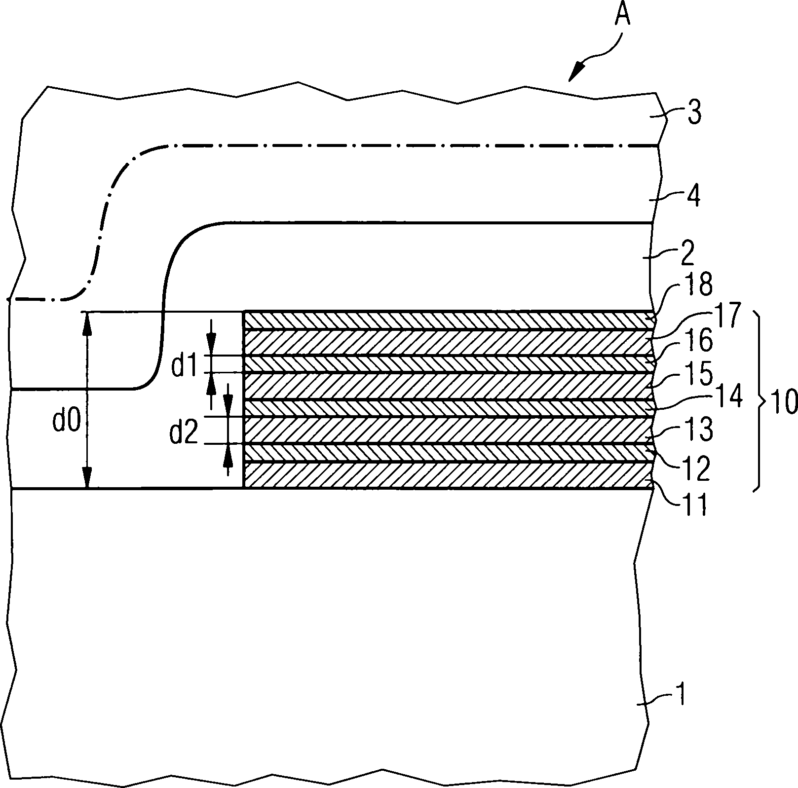
Das erfindungsgemäße Halbleiterbauelement weist einen Halbleiterkörper auf, auf den aufeinanderfolgend eine Metallisierung, ein Dielektrikum und eine mit dem Dielektrikum verbundene Pressmasse aufgebracht sind. Dabei ist die Metallisierung aus abwechselnd aufeinanderfolgend angeordneten Metallisierungsschichten bzw. Trennschichten gebildet.The inventive semiconductor device has a semiconductor body on, on the succession a metallization, a dielectric and a compound bonded to the dielectric is applied. The metallization is alternately consecutive arranged metallization layers or separating layers formed.
Gemäß einer bevorzugten Ausführungsform der Erfindung ist die Pressmasse zumindest abschnittweise unmittelbar mit dem Dielektrikum verbunden.According to one preferred embodiment of Invention is the molding compound at least in sections directly connected to the dielectric.
Die Metallisierungen dienen vornehmlich zur Herstellung elektrisch gut leitender Verbindungen. Um eine bestimmte Stromtragfähigkeit zu erreichen, sind solche Metallisierungen insbesondere bei Leistungshalbleiterbauelementen daher verhältnismäßig dick ausgebildet. Wie nachstehend näher erläutert, verringert sich jedoch bei dicken, gut leitenden Metallisierungen unter Einwirkung starker und häufiger Temperaturschwankungen und der damit verbundenen thermischen Längenänderungen deren Duktilität sowie deren Fließverhalten stärker als bei dünnen Metallisierungsschichten aus dem gleichen Material.The Metallizations serve primarily for the production of electrically good conductive connections. To a certain ampacity to achieve such metallizations, especially in power semiconductor devices therefore relatively thick educated. As closer below explained, reduced However, in thick, well-conducting metallizations under action strong and frequent temperature fluctuations and the associated thermal length changes their ductility and their flow behavior stronger as with thin metallization layers from the same material.
Um die damit verbundenen Nachteile zu vermeiden, ist es bei der vorliegenden Erfindung vorgesehen, die Metallisierung als Schichtfolge aus mehreren Metallisierungsschichten bzw. Trennschichten aufzubauen. Dazu werden Metallisierungsschichten und Trennschichten abwechselnd aufeinanderfolgend angeordnet, wobei die Metallisierungsschichten vornehmlich zur Stromführung dienen, während die Trennschichten überwiegend dazu vorgesehen sind, die Metallisierungsschichten voneinander zu trennen.Around to avoid the associated disadvantages, it is in the present Invention provided, the metallization as a layer sequence of several Build up metallization layers or separation layers. To do this Metallization layers and separation layers alternately successive arranged, wherein the metallization layers serve primarily to conduct electricity, while the separating layers predominantly are provided to the metallization layers from each other separate.
Aus
der
Des
weiteren weist die in der
Als Trennschichten eignen sich grundsätzlich alle elektrisch leitfähigen Materialien, bevorzugt Titan, Wolfram, Tantal, Kupfer, Gold, Silber oder Legierungen zumindest eines dieser Metalle, beispielsweise Titannitrid, Titanwolfram oder Tantalnitrid. Ebenso sind jedoch auch Zinkoxid, Graphit oder andere nicht-metallische Leiter als Trennschicht-Material verwendbar. Dabei können verschiedene Trennschichten aus unterschiedlichen Materialien gebildet sein. Der spezifische elektrische Widerstand der Trennschichten beträgt bevorzugt weniger als 25 μΩ·m, besonders bevorzugt weniger als 2,5 μΩ·m.When Separating layers are basically all electrically conductive materials, preferably titanium, tungsten, tantalum, copper, gold, silver or alloys at least one of these metals, for example titanium nitride, titanium tungsten or tantalum nitride. Likewise, however, zinc oxide, graphite or other non-metallic conductors can be used as the interface material. It can different separating layers may be formed of different materials. The specific electrical resistance of the separating layers is preferred less than 25 μΩ · m, especially preferably less than 2.5 μΩ · m.
Die Metallisierungsschichten hingegen sind vorzugsweise aus elektrisch gut leitenden Materialien, beispielsweise aus Aluminium, Kupfer, Gold, Silber, Wolfram oder einer Legierung zumindest eines dieser Metalle gebildet, wobei verschiedene Metallisierungsschichten aus unterschiedlichen Metallen gebildet sein können. Der spezifische elektrische Widerstand einer Metallisierungsschicht beträgt bevorzugt weniger als 0,06 μΩ·m, beispielsweise bei Wolfram etwa 0,054 μΩ·m, besonders bevorzugt weniger als 0,03 μΩ·m, beispielsweise bei Kupfer etwa 0,017 μΩ·m oder bei Aluminium etwa 0,027 μΩ·m.The By contrast, metallization layers are preferably made of electrical material highly conductive materials, such as aluminum, copper, Gold, silver, tungsten or an alloy of at least one of these Metals formed, with different metallization layers different metals can be formed. The specific electric Resistance of a metallization layer is preferably less than 0.06 μΩ · m, for example in tungsten about 0.054 μΩ · m, especially preferably less than 0.03 μΩ · m, for example for copper about 0.017 μΩ · m or for aluminum, about 0.027 μΩ · m.
Bei dem geschichteten Aufbau der Metallisierung sind die Metallisierungsschichten mittels dünner Trennschichten voneinander getrennt.at The layered structure of the metallization are the metallization layers by means of thinner Separating layers separated from each other.
Wie oben erwähnt ändern sich mit der Dicke einer Metallisierungsschicht auch deren physikalische Eigenschaften wie Fließverhalten oder Duktilität. Je dünner eine Metallisie rungsschicht ausgebildet ist, desto härter ist sie, desto geringer ist ihre Duktilität und desto weniger neigt sie zum Fließen.As mentioned above change with the thickness of a metallization layer also their physical Properties like flow behavior or ductility. The thinner a metallization layer is formed, the harder it is They, the lower their ductility and the less they tend to flow.
Somit lassen sich die eingangs erwähnten, insbesondere temperaturwechselbedingten Veränderungen der Metallisierung mittels eines geschichteten, wie oben beschriebenen, Aufbaus der Metallisierung deutlich reduzieren. Hierdurch werden die auf das Dielektrikum wirkenden mechanischen Spannungen hinsichtlich Ihrer Stärke begrenzt, wodurch sich die Wahrscheinlichkeit einer Rissbildung in einem mit der Metallisierung verbundenem Dielektrikum deutlich verringert.Consequently can be mentioned at the outset, in particular temperature changes the metallization by means of a layered, as described above, Significantly reduce the structure of the metallization. This will be with regard to the mechanical stresses acting on the dielectric Your strength limited, which increases the likelihood of cracking in a connected to the metallization dielectric clearly reduced.
Gemäß einer bevorzugten Ausführungsform ist das Dielektrikum schichtartig, beispielsweise als Passivierungsschicht oder als Oxidschicht ausgebildet. Das Dielektrikum ist typischerweise aus sprödem Material, beispielsweise aus Siliziumnitrid, oder Siliziumoxinitrid oder Siliziumdioxid gebildet.According to one preferred embodiment the dielectric layer, for example as a passivation layer or formed as an oxide layer. The dielectric is typical made of brittle material, for example, silicon nitride, or silicon oxynitride or silicon dioxide educated.
Die bevorzugten Dicken der Trennschichten liegen zwischen 1 nm und 40 nm, besonders bevorzugt zwischen 1 nm und 30 nm, während die bevorzugten Dicken der Metallisierungsschichten zwischen 1 nm und 1000 nm, besonders bevorzugt zwischen 10 nm und 1000 nm, betragen.The preferred thicknesses of the separation layers are between 1 nm and 40 nm, more preferably between 1 nm and 30 nm, while the preferred thicknesses of the metallization layers between 1 nm and 1000 nm, more preferably between 10 nm and 1000 nm.
Gemäß einer weiteren bevorzugten Ausführungsform sollte das Verhältnis zwischen der Dicke der Metallisierungsschichten und der Dicke der Trennschichten zwischen 1 und 1000 betragen. Die Metallisierung insgesamt weist eine Dicke von vorzugsweise zwischen 500 nm und 500 μm auf.According to one another preferred embodiment should the ratio between the thickness of the metallization layers and the thickness of the separation layers between 1 and 1000. The metallization has total a thickness of preferably between 500 nm and 500 μm.
Durch den geschichteten Aufbau der Metallisierung lassen sich Fließspannungen der Metallisierung von über 200 MPa oder gar über 300 MPa erreichen.By The layered structure of the metallization can yield yield stress the metallization of over 200 MPa or even over Reach 300 MPa.
Mit der in der beschriebenen Weise geschichtet aufgebauten Metallisierung lassen sich die mechanischen Eigenschaften der Trennschichten mit den guten Leitereigenschaften der Metallisierungsschichten kombinieren.With the layered in the manner described metallization can the mechanical properties of the separating layers with the combine good conductor properties of the metallization layers.
Die Erfindung wird nachfolgend anhand der beigefügten Figuren näher erläutert. In diesen zeigenThe The invention will be explained in more detail with reference to the accompanying figures. In show this
In den Figuren bezeichnen gleiche Bezugszeichen gleich Teile mit gleicher Bedeutung.In the same reference numerals designate like parts with the same Importance.
Bei
dem gezeigten Aufbau kann zwischen dem Dielektrikum
Gemäß einer
bevorzugten Ausführungsform der
Erfindung sind die Trennschichten
Die
Metallisierungsschichten
Die
Duktilität
einer Schicht
Die
oberste, vom Halbleiterkörper
Anhand
der in den
Der
einfachste Fall einer derartigen Spannungs-Dehnungs-Kurve ist in
Wie
aus der Spannungs-Dehnungs-Kurve gemäß
Anders
ist das Spannungs-Dehnungs-Verhalten duktiler Materialien, aus denen
beispielsweise die Metallisierungsschichten
Die
physikalischen Eigenschaften des betreffenden Materials haben sich
damit verändert.
Für dieses
derart veränderte
Material gilt nun eine neue Spannungs-Dehnungs-Kurve, deren Verlauf
qualitativ der Spannungs-Dehnungs-Kurve gemäß
Durch
den erfindungsgemäßen geschichteten
Aufbau der Metallisierung
Die
Dicken d2 der in
Die
dem Halbleiterkörper
Eine
Metallisierung
Die Trennschichten dienen in erster Linie dazu, die Metallisierungsschichten voneinander zu trennen. Die Dicke der Trennschichten sollte dabei so dünn wie möglich gewählt werden, allerdings mindestens so dick, dass sie auch nach dem Durchlaufen mehrerer Temperaturwechselzyklen, wie sie typischerweise bei der Inbetriebnahme bzw. bei Funktionstests eines erfindungsgemäßen Halbleiterbauelements durchlaufen werden, noch als Schicht vorliegt und nicht infolge von Diffusionsvorgängen aufgelöst wurde.The Separation layers serve primarily to the metallization layers separate from each other. The thickness of the separating layers should be so thin as possible chosen be, however, at least so thick that they also after passing through several cycles of thermal cycling, as typically in the Commissioning or functional tests of a semiconductor device according to the invention be passed through, still present as a layer and not as a result of diffusion processes was dissolved.
Zur Kontaktierung von Metallisierungen eines Halbleiterbauelementes werden häufig Bondverbindungen eingesetzt. Die Qualität und die Dauerhaftigkeit derartiger Bondverbindungen hängt jedoch unter anderem von der Dicke des Materials ab, auf das gebondet wird. Da die Metallisierungsschichten einer erfindungsgemäßen Metallisierung bevorzugt sehr dünn ausgebildet sind, ist gemäß einer bevorzugten Ausführungsform der Erfindung vorgesehen, eine der Schichten der Metallisierung, die mittels einer Bondverbindung kontaktiert werden soll, mit einer Bondmetallisierung zu versehen.to Contacting of metallizations of a semiconductor device become common Bond connections used. The quality and durability of such Bonding hangs however, inter alia, on the thickness of the material, on the bonded becomes. Since the metallization layers of a metallization according to the invention preferably very thin are formed, is in accordance with a preferred embodiment the invention provides one of the layers of metallization, which is to be contacted by means of a bond, with a Bond metallization to provide.
Eine
solche Anordnung ist in
Auf
der obersten Metallisierungsschicht
Zwischen
der Bondmetallisierung
Auf
der Metallisierung
- 11
- HalbleiterkörperSemiconductor body
- 22
- Dielektrikumdielectric
- 33
- Pressmassemolding compound
- 44
- Pufferschichtbuffer layer
- 1010
- Metallisierungmetallization
- 11, 13, 15, 1711 13, 15, 17
- Metallisierungsschichtmetallization
- 12, 14, 16, 1812 14, 16, 18
- TrennschichtInterface
- 2020
- BondmetallisierungBondmetallisierung
- 2121
- Bonddrahtbonding wire
- d0d0
- Dicke der Metallisierungthickness the metallization
- d1d1
- Dicke der Trennschichtthickness the separation layer
- d2d2
- Dicke der Metallisierungsschichtthickness the metallization layer
- d3d3
- Dicke der Bondmetallisierungthickness the bonding metallization
- 1, 101, 10
- Länge der MetallisierungLength of metallization
- Δl.DELTA.l
- Längenänderung der Metallisierungchange in length the metallization
- ε, εB, εF, ε11, ε10 ∈, ∈ B , ∈ F , ∈ 11 , ∈ 10
- Dehnungstrain
- σ, σB, σ1,σ, σ B , σ 1 ,
- Spannungtension
Claims (23)
Priority Applications (2)
| Application Number | Priority Date | Filing Date | Title |
|---|---|---|---|
| DE102004036140A DE102004036140A1 (en) | 2004-07-26 | 2004-07-26 | Semiconductor device |
| US11/191,150 US20060035458A1 (en) | 2004-07-26 | 2005-07-26 | Semiconductor element |
Applications Claiming Priority (1)
| Application Number | Priority Date | Filing Date | Title |
|---|---|---|---|
| DE102004036140A DE102004036140A1 (en) | 2004-07-26 | 2004-07-26 | Semiconductor device |
Publications (1)
| Publication Number | Publication Date |
|---|---|
| DE102004036140A1 true DE102004036140A1 (en) | 2006-03-23 |
Family
ID=35800513
Family Applications (1)
| Application Number | Title | Priority Date | Filing Date |
|---|---|---|---|
| DE102004036140A Withdrawn DE102004036140A1 (en) | 2004-07-26 | 2004-07-26 | Semiconductor device |
Country Status (2)
| Country | Link |
|---|---|
| US (1) | US20060035458A1 (en) |
| DE (1) | DE102004036140A1 (en) |
Cited By (3)
| Publication number | Priority date | Publication date | Assignee | Title |
|---|---|---|---|---|
| DE102007003281A1 (en) * | 2007-01-23 | 2008-07-24 | Epcos Ag | Piezoelectric transformer and transformer arrangement |
| DE102005019574B4 (en) * | 2005-04-27 | 2009-07-30 | Infineon Technologies Ag | Contacting arrangement for a semiconductor device |
| DE102004059389B4 (en) * | 2004-12-09 | 2012-02-23 | Infineon Technologies Ag | Semiconductor device with compensation metallization |
Families Citing this family (4)
| Publication number | Priority date | Publication date | Assignee | Title |
|---|---|---|---|---|
| US8093598B2 (en) * | 2006-03-22 | 2012-01-10 | Mitsubishi Electric Corporation | Power semiconductor device |
| US8736054B2 (en) * | 2011-07-27 | 2014-05-27 | Infineon Technologies Ag | Multilayer metallization with stress-reducing interlayer |
| CN109671668B (en) * | 2018-12-20 | 2021-04-23 | 中芯集成电路(宁波)有限公司 | A method of manufacturing a semiconductor device |
| US20230187343A1 (en) * | 2021-12-09 | 2023-06-15 | International Business Machines Corporation | Top via interconnect structure with texture suppression layers |
Citations (4)
| Publication number | Priority date | Publication date | Assignee | Title |
|---|---|---|---|---|
| US4097889A (en) * | 1976-11-01 | 1978-06-27 | Rca Corporation | Combination glass/low temperature deposited Siw Nx Hy O.sub.z |
| EP0273629A2 (en) * | 1986-12-29 | 1988-07-06 | Inmos Corporation | Transition metal clad interconnect for integrated circuits |
| EP0606813A2 (en) * | 1992-12-29 | 1994-07-20 | International Business Machines Corporation | Process for corrosion free multi-layer metal conductors |
| EP0720234A2 (en) * | 1994-12-30 | 1996-07-03 | SILICONIX Incorporated | Vertical power MOSFET having thick metal layer to reduce distributed resistance and method of fabricating the same |
Family Cites Families (6)
| Publication number | Priority date | Publication date | Assignee | Title |
|---|---|---|---|---|
| JPS56150830A (en) * | 1980-04-25 | 1981-11-21 | Hitachi Ltd | Semiconductor device |
| US5518805A (en) * | 1994-04-28 | 1996-05-21 | Xerox Corporation | Hillock-free multilayer metal lines for high performance thin film structures |
| JP3425311B2 (en) * | 1996-03-04 | 2003-07-14 | 株式会社東芝 | Negative photosensitive polymer resin composition, pattern forming method using the same, and electronic component |
| US6528343B1 (en) * | 1999-05-12 | 2003-03-04 | Hitachi, Ltd. | Semiconductor device its manufacturing method and electronic device |
| US7642649B2 (en) * | 2003-12-01 | 2010-01-05 | Texas Instruments Incorporated | Support structure for low-k dielectrics |
| US20060012014A1 (en) * | 2004-07-15 | 2006-01-19 | International Business Machines Corporation | Reliability of low-k dielectric devices with energy dissipative layer |
-
2004
- 2004-07-26 DE DE102004036140A patent/DE102004036140A1/en not_active Withdrawn
-
2005
- 2005-07-26 US US11/191,150 patent/US20060035458A1/en not_active Abandoned
Patent Citations (4)
| Publication number | Priority date | Publication date | Assignee | Title |
|---|---|---|---|---|
| US4097889A (en) * | 1976-11-01 | 1978-06-27 | Rca Corporation | Combination glass/low temperature deposited Siw Nx Hy O.sub.z |
| EP0273629A2 (en) * | 1986-12-29 | 1988-07-06 | Inmos Corporation | Transition metal clad interconnect for integrated circuits |
| EP0606813A2 (en) * | 1992-12-29 | 1994-07-20 | International Business Machines Corporation | Process for corrosion free multi-layer metal conductors |
| EP0720234A2 (en) * | 1994-12-30 | 1996-07-03 | SILICONIX Incorporated | Vertical power MOSFET having thick metal layer to reduce distributed resistance and method of fabricating the same |
Non-Patent Citations (2)
| Title |
|---|
| Widmann, Dietrich, et. al.: "Technologie hochinte- grierter Schaltungen", 2. Aufl., Springer, 1996, ISBN 3-540-59357-8, S.: 307-308 |
| Widmann, Dietrich, et. al.: "Technologie hochinte-grierter Schaltungen", 2. Aufl., Springer, 1996, ISBN 3-540-59357-8, S.: 307-308 * |
Cited By (3)
| Publication number | Priority date | Publication date | Assignee | Title |
|---|---|---|---|---|
| DE102004059389B4 (en) * | 2004-12-09 | 2012-02-23 | Infineon Technologies Ag | Semiconductor device with compensation metallization |
| DE102005019574B4 (en) * | 2005-04-27 | 2009-07-30 | Infineon Technologies Ag | Contacting arrangement for a semiconductor device |
| DE102007003281A1 (en) * | 2007-01-23 | 2008-07-24 | Epcos Ag | Piezoelectric transformer and transformer arrangement |
Also Published As
| Publication number | Publication date |
|---|---|
| US20060035458A1 (en) | 2006-02-16 |
Similar Documents
| Publication | Publication Date | Title |
|---|---|---|
| DE10358686B4 (en) | Crimpkontaktelement | |
| DE102016201071B4 (en) | semiconductor device | |
| DE112016001142T5 (en) | Power semiconductor device | |
| EP2685492B1 (en) | Power semiconductor module with at least one stress-reducing adjustment element | |
| EP3425665B1 (en) | Method for the production of a bonding wire | |
| DE112010005383B4 (en) | Semiconductor device | |
| DE102004036140A1 (en) | Semiconductor device | |
| DE102006025870A1 (en) | Bonding wire for connecting pad and pin of chip, has outer and inner layers, where inner layer has high conductivity, low bending stiffness, low breaking load and low tensile strength than that of outer layers and wire is designed as tape | |
| DE102004048688B4 (en) | Power semiconductor device | |
| DE102008033410B4 (en) | Power electronic connection device with a power semiconductor component and manufacturing method for this purpose | |
| DE69207507T2 (en) | PCB | |
| DE1279201B (en) | Semiconductor device | |
| DE102004059389B4 (en) | Semiconductor device with compensation metallization | |
| DE102009045184A1 (en) | Bond connection between a bonding wire and a power semiconductor chip | |
| DE102010001666A1 (en) | Electrical or electronic composite component e.g. junction FET (JFET) has connection layer and interlayer whose active compound is arranged on attaching layers along opposite side of sinter layers | |
| DE3514253A1 (en) | SEMICONDUCTOR DEVICE | |
| DE102004036905A1 (en) | Vertical power semiconductor device with a semiconductor chip and method for producing the same | |
| DE102004043020B3 (en) | Bonding wire and bond connection | |
| DE102016117389B4 (en) | Power semiconductor chip and method for producing a power semiconductor chip and power semiconductor device | |
| EP2232599B1 (en) | Piezoelectric multilayer component | |
| DE102013200308A1 (en) | Bonding wire for use in power-electronic module and electrical component, has filament whose melting temperature at specific pressure is higher than melting temperature of matrix at specific pressure | |
| EP3054480B1 (en) | Contact assembly and power module | |
| DE102005044510B4 (en) | Semiconductor device with front side metallization and method for its production and power diode | |
| DE2022717A1 (en) | Semiconductor component | |
| WO2013171084A2 (en) | Electric contact structure for semiconductors |
Legal Events
| Date | Code | Title | Description |
|---|---|---|---|
| OP8 | Request for examination as to paragraph 44 patent law | ||
| R002 | Refusal decision in examination/registration proceedings | ||
| R119 | Application deemed withdrawn, or ip right lapsed, due to non-payment of renewal fee |
Effective date: 20120201 |