DE102009045184A1 - Bond connection between a bonding wire and a power semiconductor chip - Google Patents
Bond connection between a bonding wire and a power semiconductor chip Download PDFInfo
- Publication number
- DE102009045184A1 DE102009045184A1 DE102009045184A DE102009045184A DE102009045184A1 DE 102009045184 A1 DE102009045184 A1 DE 102009045184A1 DE 102009045184 A DE102009045184 A DE 102009045184A DE 102009045184 A DE102009045184 A DE 102009045184A DE 102009045184 A1 DE102009045184 A1 DE 102009045184A1
- Authority
- DE
- Germany
- Prior art keywords
- power semiconductor
- layer
- semiconductor device
- bonding wire
- sub
- Prior art date
- Legal status (The legal status is an assumption and is not a legal conclusion. Google has not performed a legal analysis and makes no representation as to the accuracy of the status listed.)
- Granted
Links
Images
Classifications
-
- H—ELECTRICITY
- H10—SEMICONDUCTOR DEVICES; ELECTRIC SOLID-STATE DEVICES NOT OTHERWISE PROVIDED FOR
- H10W—GENERIC PACKAGES, INTERCONNECTIONS, CONNECTORS OR OTHER CONSTRUCTIONAL DETAILS OF DEVICES COVERED BY CLASS H10
- H10W72/00—Interconnections or connectors in packages
- H10W72/071—Connecting or disconnecting
- H10W72/075—Connecting or disconnecting of bond wires
-
- H—ELECTRICITY
- H10—SEMICONDUCTOR DEVICES; ELECTRIC SOLID-STATE DEVICES NOT OTHERWISE PROVIDED FOR
- H10W—GENERIC PACKAGES, INTERCONNECTIONS, CONNECTORS OR OTHER CONSTRUCTIONAL DETAILS OF DEVICES COVERED BY CLASS H10
- H10W72/00—Interconnections or connectors in packages
- H10W72/071—Connecting or disconnecting
- H10W72/075—Connecting or disconnecting of bond wires
- H10W72/07551—Connecting or disconnecting of bond wires characterised by changes in properties of the bond wires during the connecting
- H10W72/07555—Connecting or disconnecting of bond wires characterised by changes in properties of the bond wires during the connecting changes in materials
-
- H—ELECTRICITY
- H10—SEMICONDUCTOR DEVICES; ELECTRIC SOLID-STATE DEVICES NOT OTHERWISE PROVIDED FOR
- H10W—GENERIC PACKAGES, INTERCONNECTIONS, CONNECTORS OR OTHER CONSTRUCTIONAL DETAILS OF DEVICES COVERED BY CLASS H10
- H10W72/00—Interconnections or connectors in packages
- H10W72/50—Bond wires
- H10W72/531—Shapes of wire connectors
- H10W72/5363—Shapes of wire connectors the connected ends being wedge-shaped
-
- H—ELECTRICITY
- H10—SEMICONDUCTOR DEVICES; ELECTRIC SOLID-STATE DEVICES NOT OTHERWISE PROVIDED FOR
- H10W—GENERIC PACKAGES, INTERCONNECTIONS, CONNECTORS OR OTHER CONSTRUCTIONAL DETAILS OF DEVICES COVERED BY CLASS H10
- H10W72/00—Interconnections or connectors in packages
- H10W72/50—Bond wires
- H10W72/551—Materials of bond wires
-
- H—ELECTRICITY
- H10—SEMICONDUCTOR DEVICES; ELECTRIC SOLID-STATE DEVICES NOT OTHERWISE PROVIDED FOR
- H10W—GENERIC PACKAGES, INTERCONNECTIONS, CONNECTORS OR OTHER CONSTRUCTIONAL DETAILS OF DEVICES COVERED BY CLASS H10
- H10W72/00—Interconnections or connectors in packages
- H10W72/50—Bond wires
- H10W72/551—Materials of bond wires
- H10W72/552—Materials of bond wires comprising metals or metalloids, e.g. silver
- H10W72/5524—Materials of bond wires comprising metals or metalloids, e.g. silver comprising aluminium [Al]
-
- H—ELECTRICITY
- H10—SEMICONDUCTOR DEVICES; ELECTRIC SOLID-STATE DEVICES NOT OTHERWISE PROVIDED FOR
- H10W—GENERIC PACKAGES, INTERCONNECTIONS, CONNECTORS OR OTHER CONSTRUCTIONAL DETAILS OF DEVICES COVERED BY CLASS H10
- H10W72/00—Interconnections or connectors in packages
- H10W72/50—Bond wires
- H10W72/59—Bond pads specially adapted therefor
-
- H—ELECTRICITY
- H10—SEMICONDUCTOR DEVICES; ELECTRIC SOLID-STATE DEVICES NOT OTHERWISE PROVIDED FOR
- H10W—GENERIC PACKAGES, INTERCONNECTIONS, CONNECTORS OR OTHER CONSTRUCTIONAL DETAILS OF DEVICES COVERED BY CLASS H10
- H10W72/00—Interconnections or connectors in packages
- H10W72/90—Bond pads, in general
- H10W72/921—Structures or relative sizes of bond pads
- H10W72/923—Bond pads having multiple stacked layers
-
- H—ELECTRICITY
- H10—SEMICONDUCTOR DEVICES; ELECTRIC SOLID-STATE DEVICES NOT OTHERWISE PROVIDED FOR
- H10W—GENERIC PACKAGES, INTERCONNECTIONS, CONNECTORS OR OTHER CONSTRUCTIONAL DETAILS OF DEVICES COVERED BY CLASS H10
- H10W72/00—Interconnections or connectors in packages
- H10W72/90—Bond pads, in general
- H10W72/931—Shapes of bond pads
- H10W72/934—Cross-sectional shape, i.e. in side view
-
- H—ELECTRICITY
- H10—SEMICONDUCTOR DEVICES; ELECTRIC SOLID-STATE DEVICES NOT OTHERWISE PROVIDED FOR
- H10W—GENERIC PACKAGES, INTERCONNECTIONS, CONNECTORS OR OTHER CONSTRUCTIONAL DETAILS OF DEVICES COVERED BY CLASS H10
- H10W72/00—Interconnections or connectors in packages
- H10W72/90—Bond pads, in general
- H10W72/951—Materials of bond pads
- H10W72/952—Materials of bond pads comprising metals or metalloids, e.g. PbSn, Ag or Cu
Landscapes
- Wire Bonding (AREA)
- Electrodes Of Semiconductors (AREA)
- Internal Circuitry In Semiconductor Integrated Circuit Devices (AREA)
Abstract
Die Erfindung betrifft eine Bondverbindung zwischen einem Bonddraht (9) und einem Leistungshalbleiterchip (1). Der Leistungshalbleiterchip (10) weist einen Halbleiterkörper (1) auf, in dem ein aktiver Zellbereich (12) mit einer Vielzahl von Zellen (15) angeordnet ist, die in einer lateralen Richtung (r) aufeinanderfolgend angeordnet und elektrisch parallel geschaltet sind. Der Halbleiterkörper (1) weist einen Oberflächenabschnitt (11') auf, der in einer zur lateralen Richtung (r) senkrechten vertikalen Richtung (v) oberhalb des aktiven Zellbereichs (12) angeordnet ist. Auf den Oberflächenabschnitt (15) ist eine Metallisierungsschicht (20) aufgebracht, auf die ein Bonddraht (9) gebondet ist. Der Bonddraht (9) besteht aus einer Legierung, die wenigstens 99 Gew.-% Aluminium (91) enthält, sowie wenigstens einen weiteren Legierungsbestandteil (92). Das Aluminium (91) weist eine Kornstruktur mit einer mittleren Korngröße (<D91>) auf, die kleiner ist als 2 µm.The invention relates to a bond connection between a bonding wire (9) and a power semiconductor chip (1). The power semiconductor chip (10) has a semiconductor body (1) in which an active cell region (12) having a plurality of cells (15) arranged successively in a lateral direction (r) and electrically connected in parallel. The semiconductor body (1) has a surface section (11 ') which is arranged above the active cell area (12) in a vertical direction (v) perpendicular to the lateral direction (r). On the surface portion (15) a metallization layer (20) is applied, on which a bonding wire (9) is bonded. The bonding wire (9) consists of an alloy containing at least 99% by weight of aluminum (91) and at least one further alloying constituent (92). The aluminum (91) has a grain structure with a mean grain size (<D91>), which is smaller than 2 microns.
Description
Die Erfindung betrifft eine Bondverbindung zwischen einem Bonddraht und einem Leistungshalbleiterchip. An einer Oberseite weisen Leistungshalbleiterchip eine Chipmetallisierung auf, auf die zur elektrischen Kontaktierung des Leistungshalbleiterchips ein oder mehrere Bonddrähte gebondet werden können.The invention relates to a bond connection between a bonding wire and a power semiconductor chip. On an upper side, the power semiconductor chip has a chip metallization, to which one or more bonding wires can be bonded for electrical contacting of the power semiconductor chip.
Während des Bondvorganges wird der Bonddraht mit einer vorgegebenen Anpresskraft gegen die Chipmetallisierung gepresst, um eine innige Verbindung zwischen dem Bonddraht und der Chipmetallisierung zu erreichen. Mit zunehmendem Durchmesser des Bonddrahtes steigt jedoch die hierzu erforderliche Anpresskraft und, sofern das Bonden mittels Ultraschallbonden erfolgt, die erforderliche Ultraschall-Leistung. Wenn es sich jedoch bei dem Leistungshalbleiterchip um ein Bauelement mit einem aktiven Zellbereich mit einer Vielzahl von elektrisch parallel geschalteten Zellen handelt, beispielsweise einen MOSFET oder einen IGBT, so besteht bei einer hohen Anpresskraft und Ultraschall-Leistung die Gefahr, dass die Zellstruktur und damit einhergehend der Leistungshalbleiterchip zerstört wird, wenn die Bondung sehr dicker Bonddrähte mit einem Durchmesser von beispielsweise mehr als 100 μm oder mehr als 300 μm oberhalb des aktiven Zellbereichs erfolgt.During the bonding process, the bonding wire is pressed against the chip metallization with a predetermined contact force in order to achieve an intimate bond between the bonding wire and the chip metallization. With increasing diameter of the bonding wire, however, the required contact force and, if the bonding is carried out by means of ultrasonic bonding, the required ultrasonic power increases. However, if the power semiconductor chip is a device having an active cell region with a plurality of cells connected electrically in parallel, for example a MOSFET or an IGBT, there is the danger that the cell structure and, associated with it, a high contact pressure and ultrasound power the power semiconductor chip is destroyed when the bonding of very thick bonding wires with a diameter of, for example, more than 100 microns or more than 300 microns above the active cell area.
Daher werden zur Bondung oberhalb aktiver Zellbereiche mit dicken Bonddrähten sehr weiche Drahtmaterialien, typischer Weise aus hochreinem Aluminium mit einem Reinheitsgrad von 99,99% oder 99,999%, eingesetzt, dessen Gefüge sich durch große Einzelkörner und eine geringe Härte auszeichnet, weshalb beim Bonden eine vergleichsweise geringe Anpresskraft und Ultraschall-Leistung erforderlich ist. Hierdurch wird der unter der Chipmetallisierung befindliche aktive Zellbereich während des Bondens weniger stark belastet als bei härteren Drahtmaterialien.Therefore, for bonding above active cell areas with thick bonding wires very soft wire materials, typically made of high-purity aluminum with a purity of 99.99% or 99.999%, used, the structure of which is characterized by large individual grains and a low hardness, which is why when bonding a comparatively low contact force and ultrasonic power is required. As a result, the active cell area located under the chip metallization is subjected to less stress during bonding than with harder wire materials.
Da sich jedoch der thermische Ausdehnungskoeffizient von Aluminum sehr stark vom thermischen Ausdehnungskoeffizienten des Halbleitermaterials, beispielsweise Silizium oder Siliziumkarbid, unterscheidet, unterliegt die Bondverbindung bei häufigen Temperaturwechseln mit großen Temperaturhüben, wie sie vor allem im Schaltbetrieb bei hohen Lastwechseln, z. B. bei Anwendungen im Traktionsbereich, auftreten, einer erheblichen Temperaturwechselbelastung. Aufgrund derartiger Temperaturwechselbelastungen verringert sich im Lauf der Zeit die Kontaktfläche zwischen dem Bonddraht und der Chipmetallisierung des Leistungshalbleiterchips, bis sich der Bonddraht schließlich von der Chipmetallisierung ablöst (”lift off”). Die erläuterte Problematik steigt im Zuge der fortschreitenden Entwicklung, die zu immer höheren zulässigen Sperrschichttemperaturen der Leistungshalbleiterchips und damit zu einer höheren Temperaturwechselbelastung führt.However, since the thermal expansion coefficient of aluminum is very different from the coefficient of thermal expansion of the semiconductor material, such as silicon or silicon carbide, the bond is subject to frequent temperature changes with large temperature strokes, as in switching operation at high load changes, z. As in applications in the traction, occur, a significant thermal cycling. Due to such thermal cycling, the contact area between the bonding wire and the chip metallization of the power semiconductor chip decreases over time until the bonding wire eventually comes off the chip metallization ("lift off"). The problem explained increases in the course of progressive development, which leads to ever higher permissible junction temperatures of the power semiconductor chips and thus to a higher thermal cycling.
Um die Gefahr einer Bonddrahtablösung zu verringern, werden bislang auch kostspielige Maßnahmen in Kauf genommen. Bei einer solchen aus der
Eine weitere solche Maßnahme besteht in einem Bondprozess mit hoher Scherfläche, wie sie in der Veröffentlichung (CD-ROM) zum Vortrag
Die Aufgabe der vorliegenden Erfindung besteht darin, eine Bondverbindung zwischen einem Bonddraht und einem Leistungshalbleiterchip bereitzustellen, die die Verwendung dicker Bonddrähte erlaubt, und die einer hohen Temperaturwechselbelastung Stand hält.The object of the present invention is to provide a bonding connection between a bonding wire and a power semiconductor chip, which allows the use of thick bonding wires, and which withstands high thermal cycling.
Diese Aufgabe wird durch eine Bondverbindung gemäß Patentanspruch 1 gelöst. Ausgestaltungen und Weiterbildungen der Erfindung sind Gegenstand von Unteransprüchen.This object is achieved by a bond according to
Bei einer solchen Bondverbindung, die zwischen einem Bonddraht und einem Leistungshalbleiterchip hergestellt ist, umfasst der Leistungshalbleiterchip einen Halbleiterkörper, in dem ein aktiver Zellbereich mit einer Vielzahl von Zellen, beispielsweise IGBT- oder MOSFET-Zellen, angeordnet ist. Die Zellen sind in einer lateralen Richtung aufeinanderfolgend angeordnet und elektrisch parallel geschaltet. Der Halbleiterkörper weist einen Oberflächenabschnitt auf, der in einer zur lateralen Richtung senkrechten vertikalen Richtung oberhalb des aktiven Zellbereichs angeordnet ist.In such a bonding connection, which is produced between a bonding wire and a power semiconductor chip, the power semiconductor chip comprises a semiconductor body in which an active cell area is arranged with a multiplicity of cells, for example IGBT or MOSFET cells. The cells are sequentially arranged in a lateral direction and electrically connected in parallel. The semiconductor body has a surface portion arranged above the active cell area in a vertical direction perpendicular to the lateral direction.
Auf den Oberflächenabschnitt ist eine Chipmetallisierungsschicht aufgebracht, auf die in der vertikalen Richtung oberhalb des aktiven Zellbereichs ein Bonddraht gebondet ist. Dieser Bonddraht besteht aus einer Legierung, die wenigstens 99 Gew.% Aluminium enthält. Das Aluminium weist eine Kornstruktur mit einer mittleren Korngröße von kleiner als 2 μm auf. Diese sehr kleine Korngröße der Aluminiumkörner wird dadurch erreicht, dass dem Aluminum des Bonddrahtes wenigstens ein Legierungsbestandteil beigemischt ist. Als Korngröße eines Korns wird in diesem Kontext die maximale Abmessung des Korns angesehen. Die mittlere Korngröße der Aluminiumkörner ist durch das arithmetische Mittel der maximalen Abmessungen aller Aluminiumkörner des Bonddrahtes gegeben. Applied to the surface portion is a chip metallization layer, to which a bonding wire is bonded in the vertical direction above the active cell area. This bonding wire is made of an alloy containing at least 99% by weight of aluminum. The aluminum has a grain structure with a mean grain size of less than 2 microns. This very small grain size of the aluminum grains is achieved in that the aluminum of the bonding wire at least one alloying ingredient is mixed. The grain size of a grain in this context is considered to be the maximum dimension of the grain. The mean grain size of the aluminum grains is given by the arithmetic mean of the maximum dimensions of all the aluminum grains of the bonding wire.
Durch die Verringerung der mittleren Korngröße der Aluminiumkörner im Vergleich zu einem hochreinen Aluminiumbonddraht steigt die mechanische Belastbarkeit der Bondverbindung, so dass die plastische Verformung der Bondstelle sinkt bzw. ein Rissfortschritt, der typischerweise an Korngrenzen entlangläuft, deutlich reduziert wird und sich damit die Lebensdauer der Bondverbindung erhöht. Durch Variation der mittleren Korngröße der Aluminiumkörner kann der Aluminiumbonddraht so angepasst werden, dass eine Rekristallisierung bei Temperaturen bis zu 150°C, bis zu 175°C, bis zu 200°C, bis zu 250°C oder bis zu 400°C verhindert oder – bei nur kurzzeitigen Temperaturbelastungen – zumindest deutlich verzögert wird.By reducing the mean grain size of the aluminum grains compared to a high-purity aluminum bond wire, the mechanical strength of the bond increases, so that the plastic deformation of the bond decreases or crack propagation, which typically runs along grain boundaries, is significantly reduced and thus the life of the bond elevated. By varying the mean grain size of the aluminum grains, the aluminum bonding wire can be adjusted to prevent or recrystallize at temperatures up to 150 ° C, up to 175 ° C, up to 200 ° C, up to 250 ° C or up to 400 ° C - At only short-term temperature loads - at least significantly delayed.
Andererseits steigt durch die Verringerung der mittleren Korngröße der Aluminiumkörner auch die Härte des Bonddrahtes. Um eine hierdurch bedingte, mögliche Beschädigung des aktiven Zellbereichs während des Bondvorganges zu begegnen, ist es vorgesehen, eine Chipmetallisierung mit ausreichender Festigkeit zu verwenden. Durch die Kombination eines harten Drahtes mit einer robusten Chipmetallisierung wird das Risiko schlechter Bondausbeuten verhindert. Eine robuste Chipmetallisierung kann auf der Verwendung eines harten Metalls für die Chipmetallisierung basieren.On the other hand, decreasing the average grain size of the aluminum grains also increases the hardness of the bonding wire. In order to counteract a possible possible damage to the active cell area during the bonding process, it is intended to use a chip metallization with sufficient strength. Combining a hard wire with a robust chip metallization avoids the risk of poor bond yields. Robust chip metallization may be based on the use of a hard metal for chip metallization.
Die Chipmetallisierung kann dabei eine erste Teilschicht aufweisen, sowie eine zweite Teilschicht, die zwischen der ersten Teilschicht und dem aktiven Zellbereich auf dem Oberflächenabschnitt angeordnet ist.In this case, the chip metallization may have a first partial layer, as well as a second partial layer, which is arranged on the surface section between the first partial layer and the active cell region.
Gemäß einem Aspekt ist die erste Teilschicht härter als der Bonddraht.In one aspect, the first sub-layer is harder than the bonding wire.
Gemäß einem anderen Aspekt der Erfindung bestehen die erste Teilschicht aus Kupfer oder einer Kupferlegierung, die härter ist als der Bonddraht, während die zweite Teilschicht eine Barriereschicht darstellen kann, welche eine Diffusion von Kupfer aus der zweiten Teilschicht in den Halbleiterkörper weitestgehend verhindert.According to another aspect of the invention, the first sub-layer of copper or a copper alloy, which is harder than the bonding wire, while the second sub-layer may constitute a barrier layer, which largely prevents diffusion of copper from the second sub-layer in the semiconductor body.
Gemäß einem noch einem anderen Aspekt der Erfindung besteht die erste Teilschicht aus siliziumfreiem Aluminium, während die zweite Teilschicht eine Barriereschicht darstellen kann, welche eine Diffusion von Aluminium aus der ersten Teilschicht in den Halbleiterkörper weitestgehend verhindert.According to yet another aspect of the invention, the first sub-layer consists of silicon-free aluminum, while the second sub-layer may constitute a barrier layer which largely prevents diffusion of aluminum from the first sub-layer into the semiconductor body.
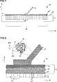
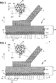
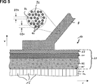
Die Erfindung wird nachfolgend anhand von Ausführungsbeispielen unter Bezugnahme auf die beigefügten Figuren beispielhaft erläutert. Es zeigen:The invention will be explained by way of example with reference to embodiments with reference to the accompanying figures. Show it:
Die gezeigten Figuren sind, sofern nichts anderes erwähnt ist, nicht maßstäblich. Die in der nachfolgenden Figurenbeschreibung verwendete, richtungsgebundene Terminologie (z. B. Begriffe wie ”oben”, ”unten”, ”links”, ”rechts”, ”vorne”, ”hinten”, ”seitlich”, ”auf”, ”unter”...) bezieht sich auf die jeweilige Figur. Sie wird lediglich dazu verwendet, das Verständnis der Figurenbeschreibung zu erleichtern. Grundsätzlich können die gezeigten Elemente räumlich beliebig angeordnet werden, sofern sich aus der Beschreibung nichts anderes ergibt. Im Übrigen bezeichnen, sofern nicht ausdrücklich anders erwähnt, in den verschiedenen Figuren gleiche Bezugszeichen gleiche oder einander entsprechende Elemente mit gleicher oder einander entsprechender Funktion.The figures shown are not to scale, unless otherwise stated. The directional terminology used in the following description of the figures (eg, terms such as "top", "bottom", "left", "right", "front", "rear", "side", "top", "bottom""...) refers to the respective figure. It is only used to facilitate the understanding of the description of the figures. Basically, the elements shown can be arranged spatially arbitrary, unless otherwise stated in the description. Incidentally, unless expressly stated otherwise, in the various figures, the same reference numerals the same or corresponding elements with the same or equivalent function.
In einer zur lateralen Richtung r senkrechten vertikalen Richtung v weist der Halbleiterkörper

Diese geringe mittlere Korngröße <D91> wird dadurch erreicht, dass der Bonddraht
Die Chipmetallisierung
Zwischen der ersten Teilschicht
Bei dem Beispiel gemäß
Die zweite Teilschicht
Eine weitere Möglichkeit, die Ausbeute beim Bonden zu erhöhen, wird anhand von
Generell eignen sich für Barriereschichten
Bei allen Varianten gemäß der vorliegenden Erfindung kann der Bonddraht die erste Teilschicht
Mit der vorliegenden Erfindung kann auf Sondermaßnahmen wie Bonddrahtversiegelung verzichtet werden. Gleichwohl kann natürlich ergänzend eine Bonddrahtversiegelung vorgesehen werden. Ein Vorteil der Erfindung besteht darin, dass die damit verbundenen Zusatzkosten weit unter denen für eine Bonddrahtversiegelung liegen. Außerdem kann eine weitere Verbesserung der Lastwechselfestigkeit im Vergleich zu bonddrahtversiegelten Modulen erreicht werden. Ein weiterer Vorteil der Erfindung liegt darin, dass die robuste Metallisierung keine Veränderung der elektrischen Parameter der Chips nach sich zieht, so dass auch produktive Chips auf einfache Weise umgestellt werden können.With the present invention can be dispensed with special measures such as bonding wire sealing. Nevertheless, of course, a bonding wire sealing can additionally be provided. An advantage of the invention is that the associated additional costs are far below those for a bonding wire seal. In addition, a further improvement in the fatigue strength compared to bond wire sealed modules can be achieved. Another advantage of the invention is that the robust metallization entails no change in the electrical parameters of the chips, so that even productive chips can be converted in a simple manner.
Die Erfindung ist an IGBTs bei einer Sperrspannung von 1,2 kV und 6,5 kV in Verbindung mit einem Bonddraht aus AlMg 0,5% (d. h. 99,5 Gew.% Al und 0,5 Gew.% Mg) und einem Durchmesser von 400 μm getestet worden. Dazu wurde der Aufbau gemäß
ZITATE ENTHALTEN IN DER BESCHREIBUNG QUOTES INCLUDE IN THE DESCRIPTION
Diese Liste der vom Anmelder aufgeführten Dokumente wurde automatisiert erzeugt und ist ausschließlich zur besseren Information des Lesers aufgenommen. Die Liste ist nicht Bestandteil der deutschen Patent- bzw. Gebrauchsmusteranmeldung. Das DPMA übernimmt keinerlei Haftung für etwaige Fehler oder Auslassungen.This list of the documents listed by the applicant has been generated automatically and is included solely for the better information of the reader. The list is not part of the German patent or utility model application. The DPMA assumes no liability for any errors or omissions.
Zitierte PatentliteraturCited patent literature
- DE 102005028951 A1 [0005] DE 102005028951 A1 [0005]
Zitierte Nicht-PatentliteraturCited non-patent literature
- Siepe, Bayerer: ”Time and spatial resolved detection of power device failures during wire bonding” auf der CIPS 2006, 4th International Conference on Integrated Power Electronics Systems, 7. bis 9. Juni 2006, Neapel/Italien, VDE-Verlag, Berlin, Frankfurt, ISBN 978-3-8007-2972-2 [0006] Siepe, Bayerer: "Time and spatial resolved detection of power device failures during wire bonding" at CIPS 2006, 4th International Conference on Integrated Power Electronics Systems, June 7 to 9, 2006, Naples / Italy, VDE-Verlag, Berlin, Frankfurt, ISBN 978-3-8007-2972-2 [0006]
Claims (20)
Priority Applications (3)
| Application Number | Priority Date | Filing Date | Title |
|---|---|---|---|
| DE102009045184.6A DE102009045184B4 (en) | 2009-09-30 | 2009-09-30 | Bond connection between a bonding wire and a power semiconductor chip |
| US12/888,781 US8541892B2 (en) | 2009-09-30 | 2010-09-23 | Bonding connection between a bonding wire and a power semiconductor chip |
| CN201010501846.5A CN102034776B (en) | 2009-09-30 | 2010-09-30 | Power semiconductor device with bonding connection between bonding wire and semiconductor chip |
Applications Claiming Priority (1)
| Application Number | Priority Date | Filing Date | Title |
|---|---|---|---|
| DE102009045184.6A DE102009045184B4 (en) | 2009-09-30 | 2009-09-30 | Bond connection between a bonding wire and a power semiconductor chip |
Publications (2)
| Publication Number | Publication Date |
|---|---|
| DE102009045184A1 true DE102009045184A1 (en) | 2011-04-28 |
| DE102009045184B4 DE102009045184B4 (en) | 2019-03-14 |
Family
ID=43796596
Family Applications (1)
| Application Number | Title | Priority Date | Filing Date |
|---|---|---|---|
| DE102009045184.6A Expired - Fee Related DE102009045184B4 (en) | 2009-09-30 | 2009-09-30 | Bond connection between a bonding wire and a power semiconductor chip |
Country Status (3)
| Country | Link |
|---|---|
| US (1) | US8541892B2 (en) |
| CN (1) | CN102034776B (en) |
| DE (1) | DE102009045184B4 (en) |
Cited By (2)
| Publication number | Priority date | Publication date | Assignee | Title |
|---|---|---|---|---|
| EP2530710A3 (en) * | 2011-06-03 | 2013-10-16 | Nippon Piston Ring Co., Ltd. | Bonding wire, connection structure, semiconductor device and manufacturing method of same |
| EP2738805A1 (en) * | 2012-11-30 | 2014-06-04 | Nippon Piston Ring Co., Ltd. | Aluminium bonding wire, connection structure, semiconductor device and manufacturing method of same |
Families Citing this family (4)
| Publication number | Priority date | Publication date | Assignee | Title |
|---|---|---|---|---|
| US9418937B2 (en) | 2011-12-09 | 2016-08-16 | Infineon Technologies Ag | Integrated circuit and method of forming an integrated circuit |
| US9087833B2 (en) | 2012-11-30 | 2015-07-21 | Samsung Electronics Co., Ltd. | Power semiconductor devices |
| KR20150002077A (en) * | 2013-06-28 | 2015-01-07 | 삼성전자주식회사 | Power semiconductor module |
| CN116384324B (en) * | 2023-06-05 | 2023-10-31 | 湖南大学 | Power module and bonding wire material determination method thereof |
Citations (4)
| Publication number | Priority date | Publication date | Assignee | Title |
|---|---|---|---|---|
| DE102004036142A1 (en) * | 2004-07-26 | 2006-03-23 | eupec Europäische Gesellschaft für Leistungshalbleiter mbH | Semiconductor component, used in power semiconductor applications, comprises a semiconductor substrate having a metallization with a barrier layer arranged between metallization layers |
| DE102004043020B3 (en) * | 2004-09-06 | 2006-04-27 | eupec Europäische Gesellschaft für Leistungshalbleiter mbH | Bonding wire and bond connection |
| DE102005028951A1 (en) | 2005-06-22 | 2006-12-28 | Infineon Technologies Ag | Arrangement for electrically connecting a semiconductor circuit arrangement with an external contact device and method for producing the same |
| DE102006052202B3 (en) * | 2006-11-06 | 2008-02-21 | Infineon Technologies Ag | Semiconductor component has metal layer comprising coherent section, and other metal layer is arranged on coherent section of former metal layer, where latter metal layer is structured between layered regions |
Family Cites Families (16)
| Publication number | Priority date | Publication date | Assignee | Title |
|---|---|---|---|---|
| JPS5928553A (en) | 1982-08-11 | 1984-02-15 | Hitachi Ltd | Corrosion resistant aluminum electronic material |
| US4845543A (en) * | 1983-09-28 | 1989-07-04 | Hitachi, Ltd. | Semiconductor device and method of manufacturing the same |
| JPS6270547A (en) * | 1985-09-25 | 1987-04-01 | Toshiba Corp | Semiconductor device |
| JPH0249447A (en) * | 1988-05-20 | 1990-02-19 | Hitachi Ltd | Semiconductor device and manufacture thereof |
| JPH01303910A (en) * | 1988-06-01 | 1989-12-07 | Hitachi Ltd | Solid-state electronic element, its manufacture and device utilizing the element |
| JP2873770B2 (en) * | 1993-03-19 | 1999-03-24 | 新日本製鐵株式会社 | Palladium fine wire for wire bonding of semiconductor devices |
| JPH07302811A (en) | 1994-05-10 | 1995-11-14 | Hitachi Ltd | Al wire for carrying large current and semiconductor module using the same |
| US5665996A (en) * | 1994-12-30 | 1997-09-09 | Siliconix Incorporated | Vertical power mosfet having thick metal layer to reduce distributed resistance |
| US6150186A (en) * | 1995-05-26 | 2000-11-21 | Formfactor, Inc. | Method of making a product with improved material properties by moderate heat-treatment of a metal incorporating a dilute additive |
| DE19603596A1 (en) | 1996-02-01 | 1997-08-07 | Zahnradfabrik Friedrichshafen | Wet clutch for high friction |
| JP3481392B2 (en) * | 1996-06-13 | 2003-12-22 | 古河電気工業株式会社 | Electronic component lead member and method of manufacturing the same |
| JP3592310B2 (en) * | 2001-06-05 | 2004-11-24 | 住友電工スチールワイヤー株式会社 | Magnesium-based alloy wire and method of manufacturing the same |
| US7960825B2 (en) * | 2006-09-06 | 2011-06-14 | Megica Corporation | Chip package and method for fabricating the same |
| JP2008311383A (en) * | 2007-06-14 | 2008-12-25 | Ibaraki Univ | BONDING WIRE, BONDING METHOD USING SAME, SEMICONDUCTOR DEVICE, AND CONNECTION STRUCTURE |
| JP4212641B1 (en) * | 2008-08-05 | 2009-01-21 | 田中電子工業株式会社 | Aluminum ribbon for ultrasonic bonding |
| US20100052174A1 (en) * | 2008-08-27 | 2010-03-04 | Agere Systems Inc. | Copper pad for copper wire bonding |
-
2009
- 2009-09-30 DE DE102009045184.6A patent/DE102009045184B4/en not_active Expired - Fee Related
-
2010
- 2010-09-23 US US12/888,781 patent/US8541892B2/en not_active Expired - Fee Related
- 2010-09-30 CN CN201010501846.5A patent/CN102034776B/en not_active Expired - Fee Related
Patent Citations (4)
| Publication number | Priority date | Publication date | Assignee | Title |
|---|---|---|---|---|
| DE102004036142A1 (en) * | 2004-07-26 | 2006-03-23 | eupec Europäische Gesellschaft für Leistungshalbleiter mbH | Semiconductor component, used in power semiconductor applications, comprises a semiconductor substrate having a metallization with a barrier layer arranged between metallization layers |
| DE102004043020B3 (en) * | 2004-09-06 | 2006-04-27 | eupec Europäische Gesellschaft für Leistungshalbleiter mbH | Bonding wire and bond connection |
| DE102005028951A1 (en) | 2005-06-22 | 2006-12-28 | Infineon Technologies Ag | Arrangement for electrically connecting a semiconductor circuit arrangement with an external contact device and method for producing the same |
| DE102006052202B3 (en) * | 2006-11-06 | 2008-02-21 | Infineon Technologies Ag | Semiconductor component has metal layer comprising coherent section, and other metal layer is arranged on coherent section of former metal layer, where latter metal layer is structured between layered regions |
Non-Patent Citations (1)
| Title |
|---|
| Siepe, Bayerer: "Time and spatial resolved detection of power device failures during wire bonding" auf der CIPS 2006, 4th International Conference on Integrated Power Electronics Systems, 7. bis 9. Juni 2006, Neapel/Italien, VDE-Verlag, Berlin, Frankfurt, ISBN 978-3-8007-2972-2 |
Cited By (2)
| Publication number | Priority date | Publication date | Assignee | Title |
|---|---|---|---|---|
| EP2530710A3 (en) * | 2011-06-03 | 2013-10-16 | Nippon Piston Ring Co., Ltd. | Bonding wire, connection structure, semiconductor device and manufacturing method of same |
| EP2738805A1 (en) * | 2012-11-30 | 2014-06-04 | Nippon Piston Ring Co., Ltd. | Aluminium bonding wire, connection structure, semiconductor device and manufacturing method of same |
Also Published As
| Publication number | Publication date |
|---|---|
| US20110121458A1 (en) | 2011-05-26 |
| US8541892B2 (en) | 2013-09-24 |
| CN102034776B (en) | 2015-06-03 |
| DE102009045184B4 (en) | 2019-03-14 |
| CN102034776A (en) | 2011-04-27 |
Similar Documents
| Publication | Publication Date | Title |
|---|---|---|
| DE102009045184B4 (en) | Bond connection between a bonding wire and a power semiconductor chip | |
| DE112016002967B4 (en) | Semiconductor device and method for manufacturing a semiconductor device | |
| DE69837690T2 (en) | Device for removing foreign matter adhered to a probe tip end surface | |
| DE112012003228B4 (en) | Semiconductor device and method of manufacturing the same | |
| DE69032879T2 (en) | Connection method for semiconductor package and connection wire for semiconductor package | |
| DE112017000426B4 (en) | POWER SEMICONDUCTOR DEVICE AND METHOD FOR PRODUCING A POWER SEMICONDUCTOR DEVICE | |
| DE102011053149C5 (en) | Die arrangement and method for processing a die | |
| DE102013208818A1 (en) | Reliable area joints for power semiconductors | |
| DE102012213548A1 (en) | Bond pad for thermocompression bonding, method of making a bond pad and device | |
| DE112011103782T5 (en) | Semiconductor element, semiconductor device and method of manufacturing a semiconductor element | |
| DE102006044691B4 (en) | Method for producing a terminal conductive structure of a component | |
| DE112013001641T5 (en) | Solar cell and method for producing a solar cell | |
| DE102014200242B4 (en) | Bonded system with coated copper conductor | |
| DE3823347A1 (en) | Power semiconductor element | |
| DE102004027176B4 (en) | Method for producing semiconductor components | |
| DE68921681T2 (en) | Flat pressure contact type semiconductor device. | |
| DE102017113515B4 (en) | Method for forming an electrically conductive contact and electronic device | |
| DE102016117389B4 (en) | Power semiconductor chip and method for producing a power semiconductor chip and power semiconductor device | |
| DE3787772T2 (en) | Semiconductor chip with a bump structure for automatic tape assembly. | |
| DE102007018854B4 (en) | Semiconductor device manufacturing method, semiconductor wafer and semiconductor device | |
| DE102004036140A1 (en) | Semiconductor device | |
| DE112019007795T5 (en) | semiconductor device | |
| DE102005044510B4 (en) | Semiconductor device with front side metallization and method for its production and power diode | |
| EP4325227A1 (en) | Tape-like composite material for test needles | |
| DE102016103967A1 (en) | Semiconductor device and manufacturing method thereof |
Legal Events
| Date | Code | Title | Description |
|---|---|---|---|
| OP8 | Request for examination as to paragraph 44 patent law | ||
| R016 | Response to examination communication | ||
| R016 | Response to examination communication | ||
| R018 | Grant decision by examination section/examining division | ||
| R020 | Patent grant now final | ||
| R082 | Change of representative | ||
| R119 | Application deemed withdrawn, or ip right lapsed, due to non-payment of renewal fee |