CN1154013C - Method and apparatus for controlling power of laser diode - Google Patents
Method and apparatus for controlling power of laser diode Download PDFInfo
- Publication number
- CN1154013C CN1154013C CNB001036505A CN00103650A CN1154013C CN 1154013 C CN1154013 C CN 1154013C CN B001036505 A CNB001036505 A CN B001036505A CN 00103650 A CN00103650 A CN 00103650A CN 1154013 C CN1154013 C CN 1154013C
- Authority
- CN
- China
- Prior art keywords
- laser diode
- signal
- periodic signal
- apc
- ram
- Prior art date
- Legal status (The legal status is an assumption and is not a legal conclusion. Google has not performed a legal analysis and makes no representation as to the accuracy of the status listed.)
- Expired - Fee Related
Links
Images


Classifications
-
- H—ELECTRICITY
- H01—ELECTRIC ELEMENTS
- H01S—DEVICES USING THE PROCESS OF LIGHT AMPLIFICATION BY STIMULATED EMISSION OF RADIATION [LASER] TO AMPLIFY OR GENERATE LIGHT; DEVICES USING STIMULATED EMISSION OF ELECTROMAGNETIC RADIATION IN WAVE RANGES OTHER THAN OPTICAL
- H01S3/00—Lasers, i.e. devices using stimulated emission of electromagnetic radiation in the infrared, visible or ultraviolet wave range
- H01S3/09—Processes or apparatus for excitation, e.g. pumping
- H01S3/091—Processes or apparatus for excitation, e.g. pumping using optical pumping
- H01S3/094—Processes or apparatus for excitation, e.g. pumping using optical pumping by coherent light
-
- G—PHYSICS
- G11—INFORMATION STORAGE
- G11B—INFORMATION STORAGE BASED ON RELATIVE MOVEMENT BETWEEN RECORD CARRIER AND TRANSDUCER
- G11B7/00—Recording or reproducing by optical means, e.g. recording using a thermal beam of optical radiation by modifying optical properties or the physical structure, reproducing using an optical beam at lower power by sensing optical properties; Record carriers therefor
- G11B7/12—Heads, e.g. forming of the optical beam spot or modulation of the optical beam
- G11B7/125—Optical beam sources therefor, e.g. laser control circuitry specially adapted for optical storage devices; Modulators, e.g. means for controlling the size or intensity of optical spots or optical traces
- G11B7/126—Circuits, methods or arrangements for laser control or stabilisation
-
- G—PHYSICS
- G11—INFORMATION STORAGE
- G11B—INFORMATION STORAGE BASED ON RELATIVE MOVEMENT BETWEEN RECORD CARRIER AND TRANSDUCER
- G11B7/00—Recording or reproducing by optical means, e.g. recording using a thermal beam of optical radiation by modifying optical properties or the physical structure, reproducing using an optical beam at lower power by sensing optical properties; Record carriers therefor
- G11B7/12—Heads, e.g. forming of the optical beam spot or modulation of the optical beam
- G11B7/125—Optical beam sources therefor, e.g. laser control circuitry specially adapted for optical storage devices; Modulators, e.g. means for controlling the size or intensity of optical spots or optical traces
- G11B7/126—Circuits, methods or arrangements for laser control or stabilisation
- G11B7/1263—Power control during transducing, e.g. by monitoring
Landscapes
- Physics & Mathematics (AREA)
- Optics & Photonics (AREA)
- Electromagnetism (AREA)
- Engineering & Computer Science (AREA)
- Plasma & Fusion (AREA)
- Optical Head (AREA)
- Optical Recording Or Reproduction (AREA)
- Semiconductor Lasers (AREA)
Abstract
一种控制激光二极管的功率的方法和设备,可防止在光盘的记录/重放区域发生的激光二极管功率波动。控制激光二极管功率的设备包括控制激光二极管的自动功率控制的控制器(APC控制器),插在递增/递减计数器与激光二极管驱动器之间,该APC控制器用于与周期同步信号同步地锁存递增/递减计数器的输出,并输出锁存结果到激光二极管驱动器。因此,可按照细分的控制模式周期性的控制激光二极管的功率电平,与通过整个模式连续控制操作相比,该激光功率电平不受外部噪声影响。
A method and apparatus for controlling the power of a laser diode to prevent laser diode power fluctuations occurring in a recording/playback area of an optical disc. The device for controlling the power of the laser diode includes a controller (APC controller) for controlling the automatic power control of the laser diode, inserted between the up/down counter and the laser diode driver, the APC controller is used to latch the increment /Down the output of the counter and output the latched result to the laser diode driver. Therefore, the power level of the laser diode can be periodically controlled according to a subdivided control mode, which is not affected by external noise compared with continuous control operation through the entire mode.
Description
技术领域technical field
本发明涉及在光记录/重放设备中将激光二极管功率控制到最佳电平的方法和设备,尤其涉及一种控制激光二极管的功率的方法和设备,可防止在光盘的记录/重放区域发生的激光二极管功率波动。The present invention relates to a method and device for controlling the power of a laser diode to an optimum level in an optical recording/reproducing device, and more particularly to a method and device for controlling the power of a laser diode to prevent Occurrence of laser diode power fluctuations.
背景技术Background technique
随着多媒体的出现,增加了对高密度记录介质的需求。这种高容量记录介质包括磁光盘驱动器(MODD),数字通用盘只读存储器(DVD-RAM)驱动器,DVD随机存取存储器(DVD-ROM)等。With the advent of multimedia, the demand for high-density recording media has increased. Such high-capacity recording media include a magneto-optical disk drive (MODD), a digital versatile disk read only memory (DVD-RAM) drive, a DVD random access memory (DVD-ROM), and the like.
这种光记录设备必须根据所用光记录介质的类型高度精确地使之最佳化。为了保证精确记录/重放数据,这种光记录设备包括一个自动激光二极管功率控制(APC)电路,用于控制施加到激光二极管(LD)的功率。Such an optical recording apparatus must be optimized with high precision according to the type of optical recording medium used. To ensure accurate recording/playback of data, this optical recording device includes an automatic laser diode power control (APC) circuit for controlling the power applied to the laser diode (LD).
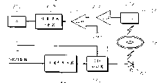
图1是常规光记录设备中APC电路结构方框图。在图1中,标号120表示一个写波形发生器,用于产生写脉冲,以按照要记录的数据形成空隔和标记,标号140表示LD驱动器,用于按照写波形发生器120产生的写脉冲控制LD 160的功率。以一种非返回到零反相(NRZI)信号的形式把要记录的数据输入到写波形发生器120。此外,在DVD-RAM的情况下,输出第一个脉冲、最后一个脉冲、冷却脉冲和多脉冲链的组合。Fig. 1 is a block diagram showing the structure of an APC circuit in a conventional optical recording apparatus. In FIG. 1,
APC电路200包括一个光电二极管(PD)202,一个可变增益放大器(VGA)204,一个比较器206,一个递增/递减计数器208和一个数模转换器210。光电二极管(PD)202接收盘180反射的激光束,并产生对应于所接收激光束的量的电流信号。可变增益放大器(VGA)204将来自光电二极管(PD)202的电流信号放大到预定增益并把电流信号转换为电压信号。比较器206比较来自可变增益放大器(VGA)204的输出与参考电压Vref,并按照比较结果输出表示二者中的那一个比另一个大的二进制判定信号。
递增/递减计数器208根据来自比较器206的比较结果执行递增或递减计数。如果比较器206的判定结果表明可变增益放大器(VGA)204的输出大于参考电压Vref,例如,如果判定信号为低,递增/递减计数器208执行递增计数。同时,如果判定信号表明可变增益放大器(VGA)204的输出小于参考电压Vref,例如,如果判定信号为高,递增/递减计数器208执行递减计数。递增/递减计数器208的计数结果通过数模转换器210施加到激光二极管(LD)驱动器140。激光二极管(LD)驱动器140按照从DAC施加的信号的幅度控制提供给LD 160的功率量。The up/down
图1的APC电路200检测LD 160的输出电平和参考电压之间的差值,该输出电平是由光电二极管(PD)202检测的,并按照所检测的差值控制提供给LD 160的功率。然而,在图1的APC电路200中,由于递增/递减计数器208的连续工作特性,即使在盘180的有效数据区域LD 160的输出与连续地变化。因此,难于得到精确的记录重放结果。此外,APC电路200对外部噪声敏感。
发明内容Contents of the invention
本发明的目的是提供一种即使在盘的有效数据区也控制供给激光二极管(LD)的功率的改进方法。It is an object of the present invention to provide an improved method of controlling the power supplied to a laser diode (LD) even in the active data area of a disc.
本发明的另一目的是提供一种用该方法控制LD的功率的设备。Another object of the present invention is to provide an apparatus for controlling the power of an LD by the method.
按照本发明的一个方面,提供一种利用光盘反射的激光电平与参考电平之间的差值控制激光二极管功率的方法,在将光盘反射的激光电平与参考电平比较之后检测该差值,该方法包括步骤:(a)产生周期信号;和(b)与周期信号同步地控制激光二极管的功率,其中所述步骤(b)包括子步骤:(b1)响应该周期信号锁存激光二极管的功率电平;(b2)比较锁存的输出电平与参考电平;以及(b3)按照在子步骤(b2)中获得的锁存输出电平与参考电平之间的差值控制激光二极管的功率电平。According to an aspect of the present invention, there is provided a method for controlling the power of a laser diode using a difference between a laser level reflected from an optical disk and a reference level, the difference being detected after comparing the laser level reflected from the optical disk with the reference level value, the method comprising the steps of: (a) generating a periodic signal; and (b) synchronously controlling the power of the laser diode with the periodic signal, wherein said step (b) includes the sub-steps of: (b1) latching the laser diode in response to the periodic signal the power level of the diode; (b2) comparing the output level of the latch with a reference level; and (b3) controlling the The power level of the laser diode.
按照本发明的另一方面,提供一种利用光盘反射的激光电平与参考电平之间的差值控制激光二极管功率的方法,在将光盘反射的激光电平与参考电平比较之后检测该差值,该方法包括步骤:(a)产生周期信号;和(b)与周期信号同步地控制激光二极管的功率,其中步骤(b)包括子步骤:(b1)与周期信号同步地对指定激光二极管功率电平的控制值采样;(b2)计算预定数目采样控制值的平均值;以及(b3)以采样控制值的平均值控制激光二极管的功率电平。According to another aspect of the present invention, there is provided a method of controlling the power of a laser diode using the difference between the laser level reflected from an optical disc and a reference level, the level of which is detected after comparing the level of laser light reflected from the disc with the reference level. difference, the method comprising the steps of: (a) generating a periodic signal; and (b) synchronously with the periodic signal to control the power of the laser diode, wherein step (b) includes the sub-steps of: (b1) synchronously with the periodic signal to the designated laser sampling the control value of the diode power level; (b2) calculating an average value of a predetermined number of sampled control values; and (b3) controlling the power level of the laser diode with the average value of the sampled control values.
按照本发明的另一方面,提供一种控制激光二极管功率的设备,它包括:光盘,用于反射光;光电二极管,用于接收该光盘反射的激光以产生对应于所接收激光的电平的电流信号;比较器,用于比较光电二极管的输出与参考电压,并输出表示该比较的那一个输入大于另一个输入的二进制判定信号;递增/递减计数器,用于按照比较器的比较结果递增/递减计数二进制判定信号;激光二极管驱动器,用于按照递增/递减计数器的计数结果控制激光二极管的功率电平;以及控制激光二极管的自动功率控制的控制器(APC控制器),插在递增/递减计数器与激光二极管驱动器之间,该APC控制器用于与周期信号同步地锁存递增/递减计数器的输出,并输出锁存结果到激光二极管驱动器。According to another aspect of the present invention, there is provided a device for controlling the power of a laser diode, which includes: an optical disc for reflecting light; a photodiode for receiving the laser light reflected by the optical disc to generate a laser light corresponding to the level of the received laser light Current signal; comparator, used to compare the output of the photodiode with the reference voltage, and output a binary decision signal indicating that the input of the comparison is greater than the other input; up/down counter, used to increment/decrement according to the comparison result of the comparator Down counting binary decision signal; laser diode driver, used to control the power level of the laser diode according to the counting result of the up/down counter; and a controller (APC controller) for controlling the automatic power control of the laser diode, inserted in the up/down Between the counter and the laser diode driver, the APC controller is used to latch the output of the up/down counter synchronously with the periodic signal, and output the latched result to the laser diode driver.
附图说明Description of drawings
通过结合附图详细描述本发明的优选实施例本发明的上述目的和优点将变得更为显而易见,附图中:The above-mentioned purposes and advantages of the present invention will become more apparent by describing in detail preferred embodiments of the present invention in conjunction with the accompanying drawings, in which:
图1是表示常规自动激光二极管功率控制(APC)电路的方框图;FIG. 1 is a block diagram representing a conventional automatic laser diode power control (APC) circuit;
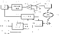
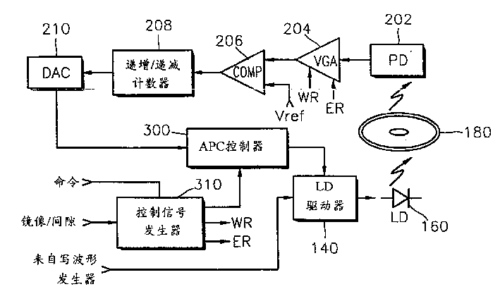
图2是表示按照本发明的用于控制供给激光二极管(LD)的功率的设备的结构方框图;2 is a block diagram showing the structure of an apparatus for controlling power supplied to a laser diode (LD) according to the present invention;
图3示出数字通用盘随机存取存储器(DVD-RAM)的扇区格式与镜像和间隙信号之间的关系;Fig. 3 shows the relationship between the sector format of a digital versatile disc random access memory (DVD-RAM) and mirror and gap signals;
图4示出表示图2设备操作的波形;Figure 4 shows waveforms representative of the operation of the device of Figure 2;
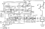
图5是表示图2设备的详细结构的方框图。FIG. 5 is a block diagram showing a detailed structure of the apparatus of FIG. 2. FIG.
具体实施方式Detailed ways
参见图2,该图是表示用于控制供给激光二极管的功率的设备(以下称为自动激光二极管功率控制(APC)电路)的结构的方框图,执行与图1中相同功能的部件用与图1中相同的标号来表示,并省略其说明。标号300表示一个APC控制器以及标号310表示一个控制信号发生器。Referring to Fig. 2, this figure is a block diagram representing the structure of a device (hereinafter referred to as an automatic laser diode power control (APC) circuit) for controlling the power supplied to a laser diode, and the parts performing the same function as in Fig. 1 are used with Fig. 1 are denoted by the same symbols as in , and their descriptions are omitted.
APC控制器300按照所选APC模式控制数模转换器210的输出。在本发明中,APC模式包括一个子APC模式,一个平均APC模式和一个子平均APC模式。子APC模式涉及APC被控制在盘的非数据记录区的模式,保持该控制值直到到达盘的下一区域。在数字通用盘随机存取存储器(DVD-RAM)中,非数据记录区包括例如镜像或间隙区。The
在平均APC模式下,来自数模转换器210的控制值与预定时间前通过在电流APC控制之前执行的APC控制获得的前一控制值的平均值被提供到激光二极管(LD)驱动器140。而且,在子平均APC模式下,得到来自盘的非数据记录区、例如镜像或间隙区的控制值的平均值,并保持该平均直到盘的下一区域。In the average APC mode, the average value of the control value from the
当施加镜像或间隙信号“镜像/间隙”时,由微计算机(未示出)控制的控制信号发生器310控制工作模式和APC控制器300的工作区域。A
图3示出DVD-RAM的扇区格式与镜像和间隙信号之间的关系。DVD-RAM的扇区基本上包括一个首标区,一个镜像区402和一个数据记录区。按照规范,用于跟踪控制的首标信号记录在首标区中,在镜像区402中不记录信号。在包括间隙区404的数据记录区中,记录扇区地址,数据等等。如图3所示,镜像信号“镜像”表示盘的镜像区402,间隙信号“间隙”表示盘的间隙区404。FIG. 3 shows the relationship between the sector format of DVD-RAM and mirror and gap signals. A sector of a DVD-RAM basically includes a header area, a mirror area 402 and a data recording area. According to the specification, a header signal for tracking control is recorded in the header area, and no signal is recorded in the mirror area 402 . In the data recording area including the
在图4中,示出说明图2中APC电路的工作的波形,波形(a)表示镜像或间隙信号“镜像/间隙”的波形,波形(b)表示图1常规APC电路中激光功率波动,其中APC在盘的整个区域的执行。此外,波形(c)到(e)示出在图2所示APC电路中分别在子APC模式、平均APC模式和子平均APC模式下的激光功率波动。In Fig. 4, the waveform illustrating the operation of the APC circuit in Fig. 2 is shown, the waveform (a) represents the waveform of the image or gap signal "mirror image/gap", and the waveform (b) represents the laser power fluctuation in the conventional APC circuit of Fig. 1, where APC is performed over the entire area of the disc. In addition, waveforms (c) to (e) show laser power fluctuations in the sub-APC mode, average APC mode, and sub-average APC mode, respectively, in the APC circuit shown in FIG. 2 .
如图4中波形(c)所示,在子APC模式下,保持锁存在镜像或间隙区末端的控制值不变直到下一镜像或间隙区。此外,在平均APC模式下,如波形(d)中所示,使用控制值的平均值,以便激光功率不会在APC范围内急剧地变化。在波形(e)中所示的子平均APC模式下,将镜像或间隙区中的控制值的平均值保持不变直到下一镜像或间隙区。As shown in waveform (c) in FIG. 4, in the sub-APC mode, the control value latched at the end of the mirror or gap region remains unchanged until the next mirror or gap region. Also, in the average APC mode, as shown in waveform (d), the average value of the control values is used so that the laser power does not vary drastically within the APC range. In the sub-average APC mode shown in waveform (e), the average value of the control values in a mirror or gap region is held constant until the next mirror or gap region.
在子APC模式或子平均APC模式下,图2的APC电路在一个扇区的时段上执行APC,因为每个扇区产生一次镜像或间隙信号“镜像/间隙”。此外,由于在非数据记录区、如镜像区或在未使用的区域、如间隙区中执行APC,不会发生激光功率的连续波动。In sub-APC mode or sub-average APC mode, the APC circuit of FIG. 2 performs APC over a period of one sector, since each sector generates a mirror or gap signal "mirror/gap". Furthermore, since APC is performed in a non-data recording area such as a mirror image area or in an unused area such as a gap area, continuous fluctuation of laser power does not occur.
在平均APC模式下,图2所示APC电路示出利用电流和前一控制值的平均值抵抗外部噪声。亦即,平均APC模式提供低通滤波控制值的作用,所以在平均APC模式下的APC操作抵抗可能包含射频(RF)分量的噪声。In average APC mode, the APC circuit shown in Fig. 2 is shown to resist external noise by using the average value of the current and the previous control value. That is, the average APC mode provides the effect of low-pass filtering the control value, so APC operation in the average APC mode is immune to noise that may contain radio frequency (RF) components.
图5是表示图2的APC电路详细结构的方框图。在图5中,用与图1所使用的那些标号的相同标号表示按与图1中相同方式执行的元件。可变增益放大器(VGA)204的增益按照控制信号WR和ER变化,控制信号WR和ER施加于其上。比较器206包括在重放模式下使用的第一比较器206a,和在擦除和记录模式下使用的第二比较器206b。递增/递减计数器208包括包括五个计数器208a至208e。第一递增/递减计数器208a用在读模式下,第二递增/递减计数器208b在擦除模式下用于槽脊,第三递增/递减计数器208c在擦除模式下用于凹槽,第四递增/递减计数器208d在擦除和记录模式下用于槽脊,和第五递增/递减计数器208e在擦除和记录模式下用于凹槽。FIG. 5 is a block diagram showing a detailed structure of the APC circuit of FIG. 2. FIG. In FIG. 5 , elements that perform in the same manner as in FIG. 1 are denoted by the same reference numerals as those used in FIG. 1 . The gain of a variable gain amplifier (VGA) 204 varies according to control signals WR and ER, to which the control signals WR and ER are applied. The
数模转换器(DAC)210包括三个数模转换器210a至210c。第一数模转换器210a用在读模式下,第二数模转换器210b用在擦除模式下,第三数模转换器210c用在记录模式下。此外,多路复用器(MUX)212包括第一和第二MUX 212a和212b,按照当前模式是擦除模式还是记录模式和当前光道是槽脊还是凹槽,该MUX将第二到第五计数器208b至208e耦合到第二和第三数模转换器210b和210c。第一MUX 212a用于在擦除模式下将第二和第三计数器208b和208c耦合到第二数模转换器210b,第二MUX 212b用于在记录模式下将第四和第五计数器208d和208e耦合到第三数模转换器。A digital-to-analog converter (DAC) 210 includes three digital-to-
包括第一至第三缓冲器(BUF)214a到214c的BUF 214在读模式下缓冲来自第一至第三数模转换器210a至210c的输出,并提供经缓冲的结构到LD驱动器140。在读模式下,第一缓冲器214a缓冲来自第一数模转换器210a的输出并输出结果到激光二极管(LD)驱动器140,第二缓冲器214b缓冲来自第二数模转换器210b的输出并输出结果到激光二极管(LD)驱动器140,第三缓冲器214c缓冲来自第三数模转换器210c的输出并输出结果到激光二极管(LD)驱动器140。The
通过锁存器216和217、第四和第五数模转换器218和219、第四和第五缓冲器在220和221、及第三多路复用器222的操作,将第一和第二参考电压Vref1和Vref2提供到比较器206。在读模式下使用的锁存器216锁存在读模式下从微计算机提供的参考数据RD1,并提供锁存的数据到第四数模转换器218。第四数模转换器218将锁存的数据转换为模拟数据,第四缓冲器220输出将来自第四数模变换器218的模拟数据作为读模式下的第一参考电压Vref1输出到第一比较器206a。在擦除和记录模式下使用的锁存器217锁存在擦除和记录模式下从微处理器提供的参考数据RD2_1,RD2_2,RD2_3和RD2_4。锁存器217包括第一到第四锁存器217a至217d。第一锁存器217a锁存用于擦除模式和槽脊的参考数据RD2_1,第二锁存器217b锁存用于擦除模式和凹槽的参考数据RD2_2,第三锁存器217c锁存用于记录模式和槽脊的参考数据RD2_3,第四锁存器217d锁存用于记录模式和凹槽的参考数据RD2_4。Through the operation of
第三多路复用器222按照当前模式是擦除模式还是记录模式和当前光道是槽脊还是凹槽而有选择地输出来自第一到第四锁存器217a至217d的输出之一。第五数模变换器219将来自第三多路复用器222的数据转换为模拟数据,第五缓冲器221将来自第五数模变换器219的模拟数据作为擦除和记录模式下的第二参考电压Vref2输出到第二比较器206b。此处,递增/递减计数器、数模变换器和比较器的数目的可变的。The
APC控制器300按照微处理器选择的APC模式控制提供到数模变换器210的值。当施加镜像或间隙信号“镜像/间隙”时,受微计算机控制的控制信号发生器310控制APC控制器300的工作模式和工作区域。分频器320将驱动器的时钟信号CK分频以产生周期信号。在具有镜像或间隙区的盘如DVD-RAM中,控制信号发生器310按照来自分频器320的分频信号DV控制APC控制器300的工作模式和工作区域。在这种情况下,周期地执行APC操作。此外,可通过改变分频器320的分频比控制APC操作的周期。The
下面按照APC模式详细说明图5所示APC电路的操作。The operation of the APC circuit shown in FIG. 5 will be described in detail below in accordance with the APC mode.
1)子APC模式1) Sub-APC mode
执行在子APC模式下,图5APC电路在一个扇区的整个周期上执行APC操作,并保持锁存在当前镜像或间隙区的控制值不变直到下一镜像或间隙区。可在整个区域中的任何点上执行在镜像或间隙区的锁存,但最好是在区域的端点。Executing in sub-APC mode, the APC circuit of FIG. 5 executes the APC operation over the entire period of a sector, and keeps the control value latched in the current mirror or gap area unchanged until the next mirror or gap area. Latching in mirror or gap regions can be performed at any point throughout the region, but preferably at the end points of the region.
由微计算机的控制设定子APC模式。在微计算机的控制下,控制信号发生器310产生控制信号,控制APC控制器300使之在子APC模式下工作。此外,控制信号可控制APC控制器300使得其在施加镜像或间隙信号“镜像/间隙”,或分频信号DV时工作。The sub-APC mode is set by the control of the microcomputer. Under the control of the microcomputer, the
当APC控制器300被镜像或间隙信号“镜像/间隙”或分频信号DV使能时,它锁存来自递增/递减计数器208或多路复用器212的信号。在本实施例中,APC控制器300可锁存并处理镜像或间隙区中的8个样本。APC控制器300锁存的控制值通过数模变换器210和缓冲器214施加到激光二极管(LD)驱动器140。The
在子APC模式下,APC控制器300在镜像或间隙信号“镜像/间隙”或分频信号DV的周期中执行锁存,这样锁存的控制值可保持不变直到施加下一镜像或间隙信号“镜像/间隙”或分频信号DV。因此,LD 160的功率可保持不变直到施加下一镜像或间隙信号“镜像/间隙”或分频信号DV。In sub-APC mode, the
2)平均APC模式2) Average APC mode
在平均APC模式下,图5的APC电路以预定周期的控制值的平均值来控制激光二极管(LD)驱动器140。由微计算机的控制设定平均APC模式。控制信号发生器310在微计算机的控制下产生控制信号,控制APC控制器300使之在平均APC模式下工作。In the average APC mode, the APC circuit of FIG. 5 controls the laser diode (LD)
APC控制器300对来自递增/递减计数器208a或多路复用器212的控制值采样并计算预定数目采样值的平均值。将该平均值通过数模转换器210和缓冲器214施加到激光二极管(LD)驱动器140。在平均APC模式下,APC控制器300以预定周期的控制值的平均值控制LD 160的功率。平均APC模式提供低通滤波控制值的作用,从而在平均APC模式下的APC操作不受外部噪声的影响,该噪声可包含射频分量。The
3)子平均APC模式3) Sub average APC mode
在子平均APC模式下,图5APC电路在一个扇区的周期中执行APC操作,并保持在镜像或间隙区期间产生的控制值的平均值不变直到下一镜像或间隙区。由微计算机的控制设定子平均APC模式。控制信号发生器310在微计算机的控制下产生控制信号,控制APC控制器300使之工作在子平均APC模式下。In the sub-average APC mode, the APC circuit of FIG. 5 performs APC operation in a sector period and keeps the average value of the control values generated during the mirror or gap period unchanged until the next mirror or gap zone. The sub-average APC mode is set by the control of the microcomputer. The
当APC控制器300被镜像或间隙信号“镜像/间隙”或分频信号DV使能时,APC控制器300计算来自递增/递减计数器208或多路复用器212的控制值的平均值,并锁存计算的平均值。在本实施例中,镜像或间隙区的8个样本被锁存和处理。APC控制器300锁存的平均值通过数模转换器210和缓中器214施加到激光二极管(LD)驱动器140。When the
在子平均APC模式下,APC控制器300在镜像或间隙信号“镜像/间隙”或分频信号DV的周期中锁存控制值的平均值,使得控制值的锁存平均值保持不变直到施加下一镜像或间隙信号“镜像/间隙”或分频信号DV。此外,以在施加镜像或间隙信号“镜像/间隙”或分频信号DV期间产生的控制值的平均值控制LD 160的功率提供执行低通滤波的作用,子平均APC模式下的APC操作抑制可包括射频分量的外部噪声。In sub-average APC mode, the
4)读模式4) Read mode
在读模式下,由一个包括锁存器216、第四数模转换器218、第四缓冲器220、第一比较器206a、第一递增/递减计数器208a、APC控制器300、第一数模转换器210a、第一缓冲器214a、激光二极管(LD)驱动器140、LD160、PD 202和VGA 204的环路执行APC操作。当初始化微计算机时,在读模式下将LD 160的所需功率电平同时存储锁存器216中。LD 160的操作用存储在锁存器216中的功率电平起动。In read mode, a system comprising a
第四数模转换器218将来自锁存器216的锁存数据转换为模拟数据,第四缓冲器220将来自第四数模转换器218的模拟数据,作为读模式的第一参考电压Vref1输出到第一比较器206a。第一递增/递减计数器208a对来自第一比较器206a的判定信号计数,第一数模转换器210a将来自第一递增/递减计数器208a的计数值转换为模拟值,第一缓冲器214a缓冲第一数模转换器210a的输出,并提供结果到激光二极管(LD)驱动器140。The fourth digital-to-
LD 160在激光二极管(LD)驱动器140的控制下输出功率,PD 202检测功率电平。所检测的功率电平通过VGA 204作为第一比较器206a的输入提供。如果LD 160的功率高于锁存器216锁存的功率电平,来自第一比较器206a的判定信号变为逻辑低,使得第一递增/递减计数器208a将判定信号递减计数一。因此,较低的控制值被施加到激光二极管(LD)驱动器140,所以来自LD160的功率电平减小。同时,如果来自LD 160的功率电平低于锁存器216锁存的功率电平,来自第一比较器206a的判定信号变为逻辑高,使得第一递增/递减计数器208a将判定信号递增计数一。因此,较高控制值被施加到激光二极管(LD)驱动器140,从而增大来自LD 160的功率电平。
上述操作继续直到来自LD 160的功率电平到达锁存器216锁存的功率电平。The above operation continues until the power level from
5)擦除模式5) Erase mode
在擦除模式下,由一个包括锁存器217、第三多路复用器222、第五数模转换器219、第五缓冲器221、第二比较器206b、第二和第三递增/递减计数器208b和208c、第一多路复用器212a、APC控制器300、第二数模转换器210b、第二缓冲器214b、激光二极管(LD)驱动器140、LD 160、PD 202和VGA 204的环路执行APC操作。当初始化微计算机时,在擦除和记录模式下将LD 160的所需功率电平同时存储在锁存器217中。LD 160的操作用存储在锁存器217中的功率电平起动。In erase mode, a circuit consisting of a
在擦除模式下,盘比如DVD-RAM的光输出必须按照光道(槽脊或凹槽)的类型改变,因此槽脊采用第一锁存器217a,凹槽采用第二锁存器217b。第三多路复用器222按照光道类型选择第一锁存器217a或第二锁存器217b的输出。具体地,使用在跟踪伺服控制电路中产生的用于识另槽脊或凹槽的信号。In erase mode, the optical output of a disc such as DVD-RAM has to be changed according to the type of track (land or groove), so the
第五数模转换器219将来自第三多路复用器222的数据转换为模拟数据,第五缓冲器221将来自第五数模转换器219的模拟数据作为擦除模式下的第二参考电压Vref2输出到第二比较器206b。递增/递减计数器208计数来自第二比较器206b的判定信号。具体地,按照光道是槽脊还是凹槽,采用用于槽脊的第二递增/递减计数器208b和用于凹槽的第三递增/递减计数器208c。第一多路复用器212a按照光道类型选择第二递增/递减计数器208b和第三递增/递减计数器208c的输出。The fifth digital-to-
第二数模转换器210b将来自第二递增/递减计数器208b或第三递增/递减计数器208c的计数值转换为模拟值,第二缓冲器214b缓冲来自第二数模转换器210b的模拟值,并将结果提供到激光二极管(LD)驱动器140。LD 160在激光二极管(LD)驱动器140的控制下输出功率,光电二极管(PD)202检测功率电平。通过VGA 204作为第二比较器206b的一个输入提供检测功率电平。The second digital-to-
6)记录模式6) Recording mode
在记录模式下,由一个包括锁存器217、第三多路复用器222、第五数模转换器219、第五缓冲器221、第二比较器206b、第四和第五递增/递减计数器208d和208e、第二多路复用器212b、APC控制器300、第三数模转换器210c、第三缓冲器214c、激光二极管(LD)驱动器140、LD 160、PD 202和VGA 204的环路执行APC操作。当初始化微计算机时,在擦除和记录模式下将LD 160的所需功率电平同时存储在锁存器217中。LD 160的操作用存储在锁存器217中的功率电平起动。In recording mode, a circuit consisting of a
在记录模式下,盘比如DVD-RAM的光输出必须按照光道(槽脊或凹槽)的类型改变,因此槽脊采用第三锁存器217c,凹槽采用第四锁存器217b。第三多路复用器222按照光道类型选择第三锁存器217c或第四锁存器217b的输出。In recording mode, the optical output of a disc such as DVD-RAM has to be changed according to the type of track (land or groove), so the
第五数模转换器219将来自第三多路复用器222的数据转换为模拟数据,第五缓冲器221将来自第五数模转换器219的模拟数据作为记录模式下的第二参考电压Vref2输出到第二比较器206b。递增/递减计数器208计数来自第二比较器206b的判定信号。具体地,按照光道是槽脊还是凹槽,采用用于槽脊的第四递增/递减计数器208d和用于凹槽的第五递增/递减计数器208e。第二多路复用器212b按照光道类型选择第四递增/递减计数器208d和第五递增/递减计数器208e的输出。The fifth digital-to-
第三数模转换器210c将来自第四递增/递减计数器208d或第五递增/递减计数器208e的计数值转换为模拟值,第三缓冲器214c缓冲来自第三数模转换器210c的模拟值,并将结果提供到激光二极管(LD)驱动器140。LD 160在激光二极管(LD)驱动器140的控制下输出功率,光电二极管(PD)202检测功率电平。通过VGA 204作为第二比较器206b的一个输入提供检测的功率电平。The third digital-to-
在本实施例中,本发明的APC电路按照三个细分的APC模式、亦即按照子APC模式、平均APC模式和子平均APC模式周期性的操作。然而,APC电路还通过整个APC模式连续地操作,如同图1所示常规APC电路。In this embodiment, the APC circuit of the present invention operates periodically according to three subdivided APC modes, namely, sub-APC mode, average APC mode and sub-average APC mode. However, the APC circuit also operates continuously through the entire APC mode, like the conventional APC circuit shown in FIG. 1 .
如上所述,按照本发明的APC电路周期性地控制LD的功率电平,不像常规APC电路具有连续工作特性,因此激光功率电平可保持恒定,并也可获得对外部噪声的抑制。此外,在非有效数据区而不是在有效数据区执行APC操作,所以可保证精确记录/重放结构。As described above, the APC circuit according to the present invention periodically controls the power level of the LD, unlike the conventional APC circuit which has continuous operation characteristics, so that the laser power level can be kept constant, and suppression of external noise can also be obtained. In addition, the APC operation is performed in the non-valid data area instead of the valid data area, so that an accurate recording/playback structure can be ensured.
虽然参照优选实施例示出和描述了本发明,本领域技术人员会理解在不偏离所附权利要求限定的本发明实质和范围的情况下可作出形式和细节上的各种更改。While the present invention has been shown and described with reference to preferred embodiments, it will be understood by those skilled in the art that various changes in form and details may be made without departing from the spirit and scope of the invention as defined in the appended claims.
Claims (20)
Applications Claiming Priority (2)
| Application Number | Priority Date | Filing Date | Title |
|---|---|---|---|
| KR1019990018848A KR100346701B1 (en) | 1999-05-25 | 1999-05-25 | Output control method of laser diode and apparatus thereof |
| KR18848/1999 | 1999-05-25 |
Publications (2)
| Publication Number | Publication Date |
|---|---|
| CN1274862A CN1274862A (en) | 2000-11-29 |
| CN1154013C true CN1154013C (en) | 2004-06-16 |
Family
ID=36500515
Family Applications (1)
| Application Number | Title | Priority Date | Filing Date |
|---|---|---|---|
| CNB001036505A Expired - Fee Related CN1154013C (en) | 1999-05-25 | 2000-02-29 | Method and apparatus for controlling power of laser diode |
Country Status (7)
| Country | Link |
|---|---|
| US (1) | US7057990B1 (en) |
| EP (1) | EP1058246B1 (en) |
| JP (1) | JP2000339736A (en) |
| KR (1) | KR100346701B1 (en) |
| CN (1) | CN1154013C (en) |
| DE (1) | DE60027816T2 (en) |
| MY (1) | MY127642A (en) |
Families Citing this family (17)
| Publication number | Priority date | Publication date | Assignee | Title |
|---|---|---|---|---|
| KR100464403B1 (en) | 2001-07-20 | 2005-01-03 | 삼성전자주식회사 | Emergency detecting apparatus of optical disk recording/reproducing device |
| KR100459702B1 (en) | 2002-02-22 | 2004-12-04 | 삼성전자주식회사 | Apparatus and method for controlling recording optical power in the optical driver |
| KR100459708B1 (en) | 2002-03-29 | 2004-12-04 | 삼성전자주식회사 | Laser diode driver having a function of auto laser power control |
| KR100505646B1 (en) * | 2002-10-24 | 2005-08-03 | 삼성전자주식회사 | Apparatus of controlling monitor PD in optical pick-up system |
| JP2006527900A (en) * | 2003-06-19 | 2006-12-07 | コーニンクレッカ フィリップス エレクトロニクス エヌ ヴィ | Means and method for generating a laser drive signal |
| KR100604820B1 (en) * | 2003-06-24 | 2006-07-26 | 삼성전자주식회사 | Automatic Laser Diode Output Control Method of Optical Disc Drive and Appropriate Device |
| EP1695344A1 (en) * | 2003-12-08 | 2006-08-30 | Koninklijke Philips Electronics N.V. | Holographic reading device |
| JP3938144B2 (en) | 2004-02-17 | 2007-06-27 | キヤノン株式会社 | Image forming apparatus, control method thereof, and control program |
| JP4715198B2 (en) * | 2004-12-27 | 2011-07-06 | ソニー株式会社 | Laser drive device |
| JP2007213680A (en) * | 2006-02-08 | 2007-08-23 | Toshiba Corp | Automatic power control filter circuit and optical disk apparatus |
| CN102111623B (en) * | 2009-12-29 | 2014-01-22 | 英特赛尔美国股份有限公司 | System and method for partitioned color, double rate video transfer |
| US8384832B2 (en) * | 2009-12-29 | 2013-02-26 | Intersil Americas Inc. | Systems and methods for partitioned color, double rate video transfer |
| JP2012018731A (en) * | 2010-07-08 | 2012-01-26 | Hitachi-Lg Data Storage Inc | Optical disk device and method for controlling laser beam power in optical disk device |
| JP2012033738A (en) * | 2010-07-30 | 2012-02-16 | Ricoh Co Ltd | Semiconductor laser drive device and image formation apparatus equipped with semiconductor laser drive device |
| JP2013093086A (en) | 2011-10-03 | 2013-05-16 | Panasonic Corp | Optical recording/reproducing device |
| KR101845662B1 (en) * | 2017-04-14 | 2018-04-05 | 이화여자대학교 산학협력단 | Vcsel diode driver circuit |
| CN117293641B (en) * | 2023-11-27 | 2024-03-01 | 深圳市通甪科技有限公司 | Laser energy feedback circuit, laser energy feedback device and laser ablation instrument |
Family Cites Families (24)
| Publication number | Priority date | Publication date | Assignee | Title |
|---|---|---|---|---|
| US3943446A (en) * | 1974-09-30 | 1976-03-09 | Westinghouse Electric Corporation | Power and modulation control system |
| DE3546599C2 (en) * | 1984-11-20 | 1993-06-03 | Olympus Optical Co., Ltd., Tokio/Tokyo, Jp | |
| JP2503202B2 (en) | 1985-01-30 | 1996-06-05 | 株式会社リコー | Output control device for semiconductor laser |
| US4856011A (en) * | 1985-01-30 | 1989-08-08 | Ricoh Company, Ltd. | Semiconductor laser control circuit |
| JPH0630031B2 (en) * | 1986-09-25 | 1994-04-20 | 日本電気株式会社 | Automatic power control circuit |
| JP2785290B2 (en) * | 1988-12-19 | 1998-08-13 | ソニー株式会社 | Optical disk seek and tracking device |
| US5146240A (en) * | 1990-02-08 | 1992-09-08 | Ricoh Company, Ltd. | Image forming apparatus with plural dot densities |
| JPH05314661A (en) * | 1992-05-08 | 1993-11-26 | Ricoh Co Ltd | Optical information recording medium |
| JPH07181605A (en) * | 1993-12-22 | 1995-07-21 | Canon Inc | Image forming device |
| JPH07251526A (en) * | 1994-01-31 | 1995-10-03 | Canon Inc | Recording device |
| US5528577A (en) * | 1994-10-19 | 1996-06-18 | Sony Corporation | Apparatus and method for reading at least partially unmetallized optical discs |
| JPH08147744A (en) * | 1994-11-16 | 1996-06-07 | Canon Inc | Optical recording device |
| JP3346073B2 (en) * | 1995-01-23 | 2002-11-18 | 株式会社日立製作所 | Disk recording medium |
| JP3260263B2 (en) * | 1995-09-27 | 2002-02-25 | 富士通株式会社 | Laser diode drive |
| DE19609575A1 (en) * | 1996-03-12 | 1997-09-18 | Thomson Brandt Gmbh | Read and write unit for different types of optical disc - has detector facility to determine focussing error, which is used to control focussing servo |
| KR100249224B1 (en) * | 1996-11-23 | 2000-03-15 | 구자홍 | The method and apparatus for detecting mirror signal |
| KR19990016023A (en) | 1997-08-12 | 1999-03-05 | 윤종용 | Laser diode light output control method and device |
| JPH11144288A (en) * | 1997-11-05 | 1999-05-28 | Yamaha Corp | Laser power control method for optical disk recording and laser diode driving circuit for optical disk recorder |
| US6310854B1 (en) * | 1997-11-28 | 2001-10-30 | Yamaha Corporation | Optical disk having areas of different recording densities or functions |
| KR100252103B1 (en) * | 1997-12-12 | 2000-05-01 | 윤종용 | Temperature compensation apparatus of laser diode and method thereof |
| JP3470584B2 (en) * | 1998-03-05 | 2003-11-25 | ヤマハ株式会社 | Optical disk recording method and apparatus |
| KR100618962B1 (en) * | 1998-08-29 | 2006-09-01 | 삼성전자주식회사 | Servo error detection method, suitable device, tracking error detection method, and tilt error detection method |
| JP2000182241A (en) * | 1998-12-16 | 2000-06-30 | Hitachi Ltd | Head amplifier and optical disk device using the same |
| US6414974B1 (en) * | 1999-09-07 | 2002-07-02 | Analog Devices, Inc. | Method and a control circuit for controlling the extinction ratio of a laser diode |
-
1999
- 1999-05-25 KR KR1019990018848A patent/KR100346701B1/en not_active Expired - Fee Related
-
2000
- 2000-02-24 EP EP00301451A patent/EP1058246B1/en not_active Expired - Lifetime
- 2000-02-24 DE DE60027816T patent/DE60027816T2/en not_active Expired - Lifetime
- 2000-02-28 MY MYPI20000756A patent/MY127642A/en unknown
- 2000-02-28 JP JP2000052002A patent/JP2000339736A/en active Pending
- 2000-02-29 CN CNB001036505A patent/CN1154013C/en not_active Expired - Fee Related
- 2000-02-29 US US09/515,101 patent/US7057990B1/en not_active Expired - Fee Related
Also Published As
| Publication number | Publication date |
|---|---|
| EP1058246B1 (en) | 2006-05-10 |
| EP1058246A2 (en) | 2000-12-06 |
| US7057990B1 (en) | 2006-06-06 |
| KR100346701B1 (en) | 2002-08-01 |
| JP2000339736A (en) | 2000-12-08 |
| DE60027816T2 (en) | 2006-10-26 |
| EP1058246A3 (en) | 2001-08-16 |
| CN1274862A (en) | 2000-11-29 |
| DE60027816D1 (en) | 2006-06-14 |
| MY127642A (en) | 2006-12-29 |
| KR20000074716A (en) | 2000-12-15 |
Similar Documents
| Publication | Publication Date | Title |
|---|---|---|
| CN1154013C (en) | Method and apparatus for controlling power of laser diode | |
| CN1185640C (en) | Laser diode output control apparatus | |
| CN1152374C (en) | Device and method for automatically controlling laser diode power | |
| CN1230813C (en) | Method for driving laser diode driver in an optical recording and reproducing apparatus | |
| CN1264146C (en) | Method of automatically optimizing writing on optical recording medium and optical recording/reproducing apparatus for performing the same | |
| CN1196555A (en) | CD device | |
| CN1181487C (en) | Playback method of disk-shaped storage medium | |
| CN1193359C (en) | Method and device for automatically controlling laser diode output | |
| CN1181472C (en) | information reproducing device | |
| CN1120480C (en) | Disc drive apparatus | |
| CN1137474C (en) | Adaptive recording method and apparatus for high-density optical recording medium | |
| CN1226725C (en) | Focus position adjustment method and system thereof | |
| US7009918B2 (en) | Information storage apparatus | |
| JP3462328B2 (en) | Spindle servo device for optical disk player | |
| US7522494B2 (en) | Control of laser emission power for recording information on optical disc | |
| CN1517987A (en) | Optical disc recording waveform control method and optical disc device using the method | |
| CN1286088C (en) | Optic disc device | |
| JP2005063546A (en) | Optical disc apparatus, laser power adjusting apparatus and laser power adjusting method | |
| CN1917050A (en) | Unit for controlling writing power inside optical recording device, and control method | |
| CN1293813A (en) | Disk device | |
| CN100423096C (en) | Optical information recording device and laser control circuit | |
| CN1482606A (en) | Apparatus and method for determining optimum recording power in a disc drive | |
| CN1697053A (en) | Optical recording device and related method | |
| JP2005203030A (en) | Optical disk device | |
| JP2003281769A (en) | Optical disc device and method for driving laser diode in the same device |
Legal Events
| Date | Code | Title | Description |
|---|---|---|---|
| C10 | Entry into substantive examination | ||
| SE01 | Entry into force of request for substantive examination | ||
| C06 | Publication | ||
| PB01 | Publication | ||
| C14 | Grant of patent or utility model | ||
| GR01 | Patent grant | ||
| ASS | Succession or assignment of patent right |
Owner name: TOSHIBA SAMSUNG STORAGE TECHNO Free format text: FORMER OWNER: SAMSUNG ELECTRONICS CO., LTD. Effective date: 20140721 |
|
| C41 | Transfer of patent application or patent right or utility model | ||
| TR01 | Transfer of patent right |
Effective date of registration: 20140721 Address after: Gyeonggi Do, South Korea Patentee after: Toshiba Samsung Storage Technology Korea Co., Address before: Gyeonggi Do, South Korea Patentee before: Samsung Electronics Co., Ltd. |
|
| CF01 | Termination of patent right due to non-payment of annual fee |
Granted publication date: 20040616 Termination date: 20170229 |
|
| CF01 | Termination of patent right due to non-payment of annual fee |