JP2005203030A - Optical disk device - Google Patents

Optical disk device Download PDF

Info

Publication number
JP2005203030A
JP2005203030A JP2004008150A JP2004008150A JP2005203030A JP 2005203030 A JP2005203030 A JP 2005203030A JP 2004008150 A JP2004008150 A JP 2004008150A JP 2004008150 A JP2004008150 A JP 2004008150A JP 2005203030 A JP2005203030 A JP 2005203030A
Authority
JP
Japan
Prior art keywords
light
current
output
laser
recording
Prior art date
Legal status (The legal status is an assumption and is not a legal conclusion. Google has not performed a legal analysis and makes no representation as to the accuracy of the status listed.)
Pending
Application number
JP2004008150A
Other languages
Japanese (ja)
Inventor
Hiroyoshi Awata
浩義 粟田
Current Assignee (The listed assignees may be inaccurate. Google has not performed a legal analysis and makes no representation or warranty as to the accuracy of the list.)
Ricoh Co Ltd
Original Assignee
Ricoh Co Ltd
Priority date (The priority date is an assumption and is not a legal conclusion. Google has not performed a legal analysis and makes no representation as to the accuracy of the date listed.)
Filing date
Publication date
Application filed by Ricoh Co Ltd filed Critical Ricoh Co Ltd
Priority to JP2004008150A priority Critical patent/JP2005203030A/en
Publication of JP2005203030A publication Critical patent/JP2005203030A/en
Pending legal-status Critical Current

Links

Images

Landscapes

  • Optical Head (AREA)

Abstract

【課題】高い記録パワーと低い再生パワーを1つのモニタ用受光素子21でモニタする場合、低い再生パワーに対する出力電圧が非常に小さく、オフセットや温度ドリフト等により制御誤差が大きくなってしまうという問題を解決する光ディスク装置を提供する。
【解決手段】レーザ光源を第1の光量レベルと該第1の光量レベルより大きい第2の光量レベルで発光させる光ディスク装置において、第1の光量レベルと第2の光量レベルのそれぞれに対応して設けられ、モニタ用受光素子の出力信号電流を電圧に変換する少なくとも2つの電流電圧変換手段22、42を備える。
【選択図】図9
When monitoring a high recording power and a low reproduction power with one monitor light receiving element 21, the output voltage for the low reproduction power is very small, and a control error becomes large due to an offset, a temperature drift, or the like. Provided is an optical disc device for solving the problem.
In an optical disc apparatus that causes a laser light source to emit light at a first light amount level and a second light amount level that is greater than the first light amount level, the laser light source corresponds to each of the first light amount level and the second light amount level. Provided is at least two current-voltage conversion means 22 and 42 for converting the output signal current of the light-receiving element for monitoring into a voltage.
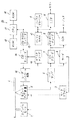
[Selection] Figure 9

Description

本発明は光ディスクに対してレーザ光により情報の記録及び再生を行う光ディスク装置に関する。   The present invention relates to an optical disc apparatus that records and reproduces information with respect to an optical disc using a laser beam.

近年、光ディスク装置においては、記録速度の上昇とともに記録パワーが高パワー化し、記録パワーと再生パワーの差が大きくなり、半導体レーザの発光パワー制御範囲が広がる傾向にあり、高い記録パワーと低い再生パワーの両方を精度良く制御することが困難になっている。
そこで、特許文献1記載の光ディスク装置では、記録スピードによって半導体レーザ駆動系のゲインを変え、これによって、半導体レーザ駆動系にて高い記録パワーと低い記録パワーを高い精度で制御している。
In recent years, in the optical disk apparatus, the recording power has been increased with an increase in recording speed, the difference between the recording power and the reproduction power has been increased, and the emission power control range of the semiconductor laser has been widened. It is difficult to control both of them accurately.
Therefore, in the optical disc apparatus described in Patent Document 1, the gain of the semiconductor laser drive system is changed according to the recording speed, and thereby, the high recording power and the low recording power are controlled with high accuracy in the semiconductor laser drive system.

特開2002−230771JP 2002-230771

上記特許文献1記載の光ディスク装置では、記録スピードによって半導体レーザ駆動系のゲインを変え、これによって、半導体レーザ駆動系にて高い記録パワーと低い記録パワーを高い精度で制御しているが、半導体レーザの光出力をモニタするモニタ系は、高い記録パワーと低い再生パワーを1つのモニタ用受光素子でモニタする場合、低い再生パワーに対する出力電圧が非常に小さくなり、オフセットや温度ドリフト等により制御誤差が大きくなってしまう。   In the optical disk device described in Patent Document 1, the gain of the semiconductor laser drive system is changed according to the recording speed, and thereby the high recording power and the low recording power are controlled with high accuracy in the semiconductor laser drive system. When monitoring high recording power and low reproduction power with a single monitor light receiving element, the output voltage for the low reproduction power becomes very small, and control errors may occur due to offset, temperature drift, etc. It gets bigger.

例えば記録パワー80mWに対して再生パワーが0.7mWであった場合、モニタ用受光素子の出力電流を電圧に変換する電流・電圧変換器に0〜5V電源のアンプを使用したとすると、出力可能範囲が約1〜4V、再生パワーに対応する基準電圧が2.5Vであるとすると、ダイナミックレンジが1.5Vになる。記録パワー80mWで上記電流・電圧変換器の出力電圧を1.5Vとすると、再生パワー0.7mWでは上記電流・電圧変換器の出力電圧は約13mVとなる。この時、温度ドリフトが1mV発生すると、再生パワーは温度ドリフトにより約8%のずれが生じてしまう。
本発明は、レーザ光源発光パワーの制御誤差を小さくすることができる光ディスク装置を提供することを目的とする。
For example, if the reproduction power is 0.7mW with respect to the recording power of 80mW, the output range is possible if the 0-5V power amplifier is used for the current / voltage converter that converts the output current of the light receiving element for monitoring into voltage. Is approximately 1 to 4 V, and the reference voltage corresponding to the reproduction power is 2.5 V, the dynamic range is 1.5 V. If the output voltage of the current / voltage converter is 1.5 V at a recording power of 80 mW, the output voltage of the current / voltage converter is about 13 mV at a reproduction power of 0.7 mW. At this time, if 1 mV of temperature drift occurs, the reproduction power will be shifted by about 8% due to temperature drift.
An object of the present invention is to provide an optical disc apparatus capable of reducing a control error of laser light source emission power.

上記目的を達成するため、請求項1に係る発明は、光ディスクに対してデータを記録再生させるためのレーザビームを照射するレーザ光源と、このレーザ光源の光出力をモニタするためのモニタ用受光素子と,このモニタ用受光素子の出力信号を用いて前記レーザ光源の出力光量を制御する制御手段とを有し、前記レーザ光源を第1の光量レベルと該第1の光量レベルより大きい第2の光量レベルで発光させる光ディスク装置において、前記第1の光量レベルと前記第2の光量レベルのそれぞれに対応して設けられ、前記モニタ用受光素子の出力信号電流を電圧に変換する少なくとも2つの電流電圧変換手段を備えたものである。   In order to achieve the above object, the invention according to claim 1 is directed to a laser light source for irradiating a laser beam for recording / reproducing data on / from an optical disc, and a light receiving element for monitoring for monitoring the light output of the laser light source. And a control means for controlling an output light amount of the laser light source using an output signal of the monitor light receiving element, and the laser light source has a second light amount level higher than the first light amount level and the second light amount level. In an optical disc apparatus that emits light at a light amount level, at least two current voltages that are provided corresponding to each of the first light amount level and the second light amount level and that convert an output signal current of the light receiving element for monitoring into a voltage. A conversion means is provided.

請求項2に係る発明は、光ディスクに対してデータを記録再生させるためのレーザビームを照射するレーザ光源と、このレーザ光源の光出力をモニタするためのモニタ用受光素子と,このモニタ用受光素子の出力信号を用いて前記レーザ光源の出力光量を制御する制御手段とを有し、前記光ディスクからデータを再生する再生時の前記光源レーザの光量レベルである第1の光量レベルと、前記光ディスクにデータを記録する記録時の前記光源レーザの光量レベルである、前記第1の光量レベルより大きい第2の光量レベルのレベル間の光量を使用して前記光ディスクに対するデータの記録再生を行う光ディスク装置において、前記第1の光量レベルと前記第2の光量レベルのそれぞれに対応して設けられ、前記モニタ用受光素子の出力信号電流を電圧に変換する少なくとも2つの電流電圧変換手段を備えたものである。   According to a second aspect of the present invention, there is provided a laser light source for irradiating a laser beam for recording and reproducing data on an optical disc, a monitor light receiving element for monitoring the light output of the laser light source, and the monitor light receiving element Control means for controlling the output light amount of the laser light source using the output signal of the first light amount level, which is the light amount level of the light source laser during reproduction for reproducing data from the optical disc, and the optical disc In an optical disc apparatus that records and reproduces data to and from the optical disc by using a light amount between a second light amount level that is a light amount level of the light source laser at the time of recording for recording data and that is larger than the first light amount level. , Provided corresponding to each of the first light quantity level and the second light quantity level, and output signal power of the monitor light receiving element. The those having at least two current-voltage conversion means for converting into a voltage.

請求項3に係る発明は、請求項1または2記載の光ディスク装置において、波長の異なる複数のレーザ光源を有し、前記少なくとも2つの電流電圧変換手段を前記レーザ光源毎に備えたものである。   According to a third aspect of the present invention, in the optical disc apparatus according to the first or second aspect, the optical disk apparatus has a plurality of laser light sources having different wavelengths, and the at least two current-voltage conversion means are provided for each of the laser light sources.

請求項4に係る発明は、請求項1、2または3記載の光ディスク装置において、前記各電流電圧変換手段はゲイン調整をそれぞれ独立して行うゲイン調整手段を有するものである。   According to a fourth aspect of the present invention, in the optical disc apparatus according to the first, second, or third aspect, each of the current-voltage conversion units includes a gain adjustment unit that performs gain adjustment independently.

請求項5に係る発明は、請求項1、2または3記載の光ディスク装置において、前記少なくとも2つの電流電圧変換手段それぞれの前記光量レベルに対する出力電圧の関係式を不揮発性記憶素子に記憶させておくものである。   According to a fifth aspect of the present invention, in the optical disk device according to the first, second, or third aspect, a relational expression of an output voltage with respect to the light amount level of each of the at least two current-voltage conversion means is stored in a nonvolatile memory element. Is.

本発明によれば、レーザ光源発光パワーの制御誤差を小さくすることができる。   According to the present invention, the control error of the laser light source emission power can be reduced.

図1は、本発明の実施形態1である光ディスク装置の概略構成を示す。
光ディスク1はスピンドルモータ2により回転駆動され、スピンドルモータ2はモータドライバ3とサーボ手段4により光ディスク1が線速度一定(CLV)または回転数一定(CAV)で回転するように制御される。
FIG. 1 shows a schematic configuration of an optical disc apparatus according to Embodiment 1 of the present invention.
The optical disk 1 is rotationally driven by a spindle motor 2, and the spindle motor 2 is controlled by a motor driver 3 and servo means 4 so that the optical disk 1 rotates at a constant linear velocity (CLV) or a constant rotational speed (CAV).

光ピックアップ装置5は、レーザ光源としての半導体レーザ(以下LDという)、光学系、フォーカシングアクチュエータ、トラッキングアクチュエータ、受光器、ポジションセンサ等を内蔵し、LDからレーザ光を光学系を介して光ディスク1の記録面に集光させる。光ピックアップ装置5は、図示しないシークモータによりスレッジ(光ディスク1の半径方向)に移動可能に設けられている。これらのフォーカシングアクチュエータ、トラッキングアクチュエータ、シークモータは、光ディスク1の記録面からの反射光を光学系を介して受光する受光器やポジションセンサからの信号に基づきモータドライバ3とサーボ手段4によって光ディスク1上のレーザ光スポットを光ディスク1上の目的の場所に位置させるように制御する。   The optical pickup device 5 includes a semiconductor laser (hereinafter referred to as LD) as a laser light source, an optical system, a focusing actuator, a tracking actuator, a light receiver, a position sensor, and the like, and laser light from the LD is passed through the optical system to the optical disk 1. Focus on the recording surface. The optical pickup device 5 is provided so as to be movable in a sledge (in the radial direction of the optical disc 1) by a seek motor (not shown). These focusing actuators, tracking actuators, and seek motors are mounted on the optical disk 1 by a motor driver 3 and servo means 4 based on signals from a light receiver or position sensor that receives reflected light from the recording surface of the optical disk 1 through an optical system. The laser beam spot is controlled to be positioned at a target location on the optical disc 1.

データ再生時には、光ピックアップ装置5で得られた再生信号は、リードアンプ6で増幅されてイコライザ処理や2値化処理がなされた後、CDデコーダ7でEFM復調される。EFM信号は、光学的に再生又は記録がしやすいように8ビットデータを14ビットデータに変調したデータであり、EFM復調されたデータはデインターリーブ(並べ替え直し処理)とエラー訂正の処理が行われる。CDデコーダ7からのデータはCD−ROMデコーダ8によりデータの信頼性を高めるためのエラー訂正処理が行われる。   At the time of data reproduction, the reproduction signal obtained by the optical pickup device 5 is amplified by the read amplifier 6 and subjected to equalizer processing and binarization processing, and then EFM demodulated by the CD decoder 7. The EFM signal is data obtained by modulating 8-bit data into 14-bit data so that it can be easily reproduced or recorded optically. The EFM demodulated data undergoes deinterleaving (reordering processing) and error correction processing. Is called. The data from the CD decoder 7 is subjected to an error correction process for improving the reliability of the data by the CD-ROM decoder 8.

CD−ROMデコーダ8からのデータは、バッファマネージャ9によって、一旦バッファRAM10に蓄積され、セクタデータとして揃ったときにインターフェース11を介してホストへ一気に転送される。また、データが音楽データである場合には、CDデコーダ7からのデータはD/Aコンバータ12によりアナログのオーディオ信号に変換されて取り出される。   The data from the CD-ROM decoder 8 is temporarily stored in the buffer RAM 10 by the buffer manager 9 and transferred to the host via the interface 11 when it is prepared as sector data. When the data is music data, the data from the CD decoder 7 is converted into an analog audio signal by the D / A converter 12 and extracted.

一方、データ記録時には、ホストから送られてきたデータがインターフェース11により受信され、そのデータがバッファマネージャ9によって一旦バッファRAM10に蓄積される。バッファRAM10にある程度のデータが蓄積されたときにデータの記録が開始されるが、その前に、レーザ光スポットが光ディスク1の書き込み開始地点に位置される。その書き込み開始地点は光ディスク1上のトラック(プリグルーブ)の蛇行によって予め刻まれているウォブル信号であるATIP(Absolute Time In Pre−groove)信号によって求められる。ATIP信号は、光ディスク1上の絶対番地を示す時間情報であり、ATIPデコーダ13によってリードアンプ6からのデータより取り出されるとともに、ATIP信号エラーが検出されてATIP信号の検出エラー率が計測される。   On the other hand, at the time of data recording, data sent from the host is received by the interface 11, and the data is temporarily stored in the buffer RAM 10 by the buffer manager 9. Data recording is started when a certain amount of data is accumulated in the buffer RAM 10, but before that, the laser beam spot is positioned at the writing start point of the optical disc 1. The writing start point is obtained by an ATIP (Absolute Time In Pre-groove) signal which is a wobble signal that is preliminarily carved by meandering tracks (pre-grooves) on the optical disk 1. The ATIP signal is time information indicating an absolute address on the optical disc 1, and is extracted from the data from the read amplifier 6 by the ATIP decoder 13, and an ATIP signal error is detected and an ATIP signal detection error rate is measured.

また、ATIPデコーダ13がリードアンプ6からのデータより生成する同期信号はCDエンコーダ14に入力されて正確な位置でのデータの書き出しが可能となる。データ記録を行うときにはバッファRAM10からデータが読み出され、このデータはCD−ROMエンコーダ15及びCDエンコーダ14でエラー訂正コードの付加やインターリーブ(並べ替え)が行われた後EFM変調され、レーザコントロール回路16、光ピックアップ装置5を介して光ディスク1に記録される。   Further, the synchronization signal generated from the data from the read amplifier 6 by the ATIP decoder 13 is input to the CD encoder 14 so that the data can be written at an accurate position. When data recording is performed, data is read from the buffer RAM 10, and after the error correction code is added and interleaved (rearranged) by the CD-ROM encoder 15 and the CD encoder 14, the data is EFM-modulated, and the laser control circuit. 16, recording is performed on the optical disc 1 via the optical pickup device 5.

この光ディスク装置は、上述の各部の動作を制御するためのCPU17、ROM18およびRAM19からなるマイクロコンピュータ20を備えている。   This optical disk apparatus includes a microcomputer 20 including a CPU 17, a ROM 18, and a RAM 19 for controlling the operation of each unit described above.

ここで、本実施形態1のLD発光パワー制御方式を説明する前に、一般的な従来のLD発光パワー制御方式について説明する。
光ディスク装置におけるデータ記録は、光ディスク、例えばCD-R(Compact Disc Recordable)ではCD-R上の記録膜に光ピックアップ装置内のLDから強いレーザ光を光ビームとして照射し、その熱反応により、光ディスクの記録膜に穴(ピット)を開けることにより行われる。また、光ディスク装置におけるデータ記録は、CD-RW(Compact Disc ReWritable)ではCD-RWの記録膜に光ピックアップ装置内のLDから強いレーザ光を光ビームとして照射して記録膜の結晶状態を変化させることによって行われる。
Here, before explaining the LD light emission power control method of the first embodiment, a general conventional LD light emission power control method will be explained.
Data recording in an optical disc apparatus is performed by irradiating a recording film on an optical disc, such as a CD-R (Compact Disc Recordable), with a strong laser beam as a light beam from the LD in the optical pickup device, and by the thermal reaction, the optical disc This is done by making holes (pits) in the recording film. For data recording in an optical disk device, in CD-RW (Compact Disc ReWritable), the recording film of the CD-RW is irradiated with a strong laser beam from the LD in the optical pickup device as a light beam to change the crystal state of the recording film. Is done by.

一方、光ディスクに書き込まれたデータはLDから発光される弱いレーザ光を光ビームとして光ディスクの記録膜上に照射して得られる反射光量を読み取ることができる。ところで、上述したように光ディスクのデータ記録はLDからの光ビームによって光ディスクにピットを開けることで行われるが、この時のレーザ光の発光パワー(CD-Rドライブ装置でLDから出射されるレーザ光の光量)は図2に示すようになっている。図2において、LDからは第1のパワーP1と、この第1のパワーP1よりも高い第2のパワーP2が繰り返し出射される。このP2が記録パワーで、光ディスク上においてP2レベルのレーザ光が照射されるところがピットとなる。また、P1は再生パワーであり、光ディスク上においてP1レベルのレーザ光が照射されるところがそのままスペースとなる。   On the other hand, the data written on the optical disk can read the amount of reflected light obtained by irradiating the recording film of the optical disk with a weak laser beam emitted from the LD as a light beam. By the way, as described above, data recording on the optical disk is performed by opening a pit on the optical disk with a light beam from the LD. At this time, the laser light emission power (the laser light emitted from the LD by the CD-R drive device) 2) is as shown in FIG. In FIG. 2, a first power P1 and a second power P2 higher than the first power P1 are repeatedly emitted from the LD. This P2 is the recording power, and the pit is where the P2 level laser beam is irradiated on the optical disk. Further, P1 is the reproduction power, and the place where the laser beam of the P1 level is irradiated on the optical disk becomes a space as it is.

CD-Rでは、P3>P2なるP3レベルを設けて、P1、P2、P3の3値で記録パワー波形を生成することがあり、P3レベルをピット先頭に位置付けるようにして、ピットエッジを先鋭化している。また、CD-RWのような相変化型の書き換え可能な光ディスクでは、LD発光パワーをやはり3値を設けるが、P3とP1を高速で繰り返すことで記録膜をアモルファス(非結晶)化し、P2を持続させることで記録膜を結晶化させ、これを情報データに対応させる。図2で時間tライトスタートより前が光ディスクからデータを再生するときのLDの発光波形、時間tライトスタートより後が光ディスクにデータを記録する場合のLDの発光波形である。上述したように光ディスクのデータを再生する再生(リード)時にLDの発光はパワーが低くてDC発光であり、一般的にP1は1mWほどである。一方、記録(ライト)時にLDが発射するレーザ光のパワーは高く、P2は一般に数mW〜数十mWである。記録時は、P1とP2の発光が繰り返されることで光ディスクにピットをつくることができる。 In the CD-R, a recording power waveform may be generated with three values P1, P2, and P3 by providing a P3 level of P3> P2, and the pit edge is sharpened by positioning the P3 level at the head of the pit. ing. In addition, in a phase change type rewritable optical disc such as CD-RW, the LD emission power is also provided with three values. By repeating P3 and P1 at high speed, the recording film is made amorphous (non-crystalline), and P2 is The recording film is crystallized by sustaining it, and this corresponds to the information data. Prior to time t write started in FIG. 2 is a light emission waveform of the LD in a case where after the emission waveform, time t write start LD at the time of reproducing data from the optical disk to record data on the optical disk. As described above, at the time of reproduction (reading) for reproducing data on the optical disc, the LD emits light with low power and DC emission, and generally P1 is about 1 mW. On the other hand, the power of the laser beam emitted by the LD during recording (writing) is high, and P2 is generally several mW to several tens mW. At the time of recording, pits can be formed on the optical disc by repeating the light emission of P1 and P2.

ところで、近年、光ディスク装置においては、再生速度、記録速度ともに上昇しつつある傾向にある。再生速度では52倍速のものもあり、記録速度も52倍速のもある。例えばCD-Rに52倍速でデータを記録する場合には、記録パワーは再生パワーに対して80倍くらいになることもある。また、LDは自らの発振による温度上昇等によってその発光パワーが変化する(特に発光パワーが高パワーであるときに温度が上昇する時間が短くなる)ので、光ディスク装置においてモニタ用受光素子でLDの光出力をモニタしながらLDを駆動する電流を制御することで、LDの発光パワーを一定にしている。   By the way, in recent years, in the optical disc apparatus, both the reproduction speed and the recording speed tend to increase. Some playback speeds are 52x, and some recording speeds are 52x. For example, when data is recorded on a CD-R at 52 times speed, the recording power may be about 80 times the reproducing power. In addition, since the emission power of LD changes due to its own temperature rise due to its own oscillation (especially when the emission power is high, the temperature rise time is shortened), the optical receiver uses a monitor light-receiving element in the LD. By controlling the current that drives the LD while monitoring the optical output, the light emission power of the LD is kept constant.

図3は従来の光ディスク装置においてLDの発光パワーを一定の発光パワーに制御するディジタルLD発光パワー制御方式の構成例を示す。LDの発光パワーを一定の発光パワーに制御する定パワー制御(以下APCという)はディジタル制御で行っている。図3において、光ピックアップ装置内のLDからモニタ用受光素子としてのフォトダイオード(以下PDという)21に入射されたレーザ光はLD21にて光電変換により入射光量に比例した電流のかたちで出力される。ただし、PD21によるレーザ光量モニタは光ピックアップ装置内のLD38からのレーザ光の一部をモニタするものであり、LD38からのレーザ光の大部分は光ディスクの記録膜へ照射される。   FIG. 3 shows a configuration example of a digital LD light emission power control method for controlling the light emission power of the LD to a constant light emission power in the conventional optical disk apparatus. Constant power control (hereinafter referred to as APC) for controlling the light emission power of the LD to a constant light emission power is performed by digital control. In FIG. 3, laser light incident on a photodiode (hereinafter referred to as PD) 21 as a light receiving element for monitoring from the LD in the optical pickup device is output in the form of a current proportional to the incident light amount by photoelectric conversion in the LD 21. . However, the laser light amount monitor by the PD 21 monitors a part of the laser light from the LD 38 in the optical pickup device, and most of the laser light from the LD 38 is irradiated to the recording film of the optical disk.

PD21から出力された電流は、電流・電圧(I/V)変換器22により電圧に変換されて電圧値として出力され、増幅器24により増幅される。I/V変換器22の出力電圧において、光量レベルP1に対応したものをV(P1)とし、光量レベルP2に対応したものをV(P2)とする。記録時におけるI/V変換器22の出力電圧は再生時と異なりV(P1)とV(P2)が交互に変化する信号であるため、増幅器24の出力電圧はサンプルホールド(S/H)回路25、26によってV(P1)とV(P2)に分離される。   The current output from the PD 21 is converted into a voltage by a current / voltage (I / V) converter 22, output as a voltage value, and amplified by an amplifier 24. In the output voltage of the I / V converter 22, V (P1) corresponds to the light level P1, and V (P2) corresponds to the light level P2. Since the output voltage of the I / V converter 22 at the time of recording is a signal in which V (P1) and V (P2) change alternately unlike at the time of reproduction, the output voltage of the amplifier 24 is a sample hold (S / H) circuit. 25 and 26 separate into V (P1) and V (P2).

S/H回路25におけるサンプル信号1は、再生時には常にS/H回路25内のスイッチ25aをオンさせる信号であり、記録時には記録時のP1のレーザ光が出射されている期間、あるいはそれより短い期間のみS/H回路25内のスイッチ25a をオンとし、また、P2のレーザ光が出射されている期間にはS/H回路25内のスイッチ25aをオフし、S/H回路25内のコンデンサ25bでP1に対応した電圧Vs(P1)のみを取り出してアンプ25cを介して出力させる信号である。   The sample signal 1 in the S / H circuit 25 is a signal that always turns on the switch 25a in the S / H circuit 25 at the time of reproduction, and at the time of recording, the period during which the P1 laser beam is emitted or shorter than that. The switch 25a in the S / H circuit 25 is turned on only during the period, and the switch 25a in the S / H circuit 25 is turned off during the period when the P2 laser beam is emitted, and the capacitor in the S / H circuit 25 is turned on. 25b is a signal for extracting only the voltage Vs (P1) corresponding to P1 and outputting it through the amplifier 25c.

一方、S/H回路26におけるサンプル信号2は、再生時には常にS/H回路26内のスイッチ26aをオフさせる信号であり、記録時にはレーザ光がP2で出射されている期間、あるいはそれより短い期間のみS/H回路26内のスイッチ26a をオンさせ、記録時にはレーザ光がP1で出射されている期間にはS/H回路26内のスイッチ26a をオフさせ、S/H回路26内のコンデンサ26bでP2に対応した電圧Vs(P2)のみを取り出してアンプ26cを介して出力させる信号である。   On the other hand, the sample signal 2 in the S / H circuit 26 is a signal that always turns off the switch 26a in the S / H circuit 26 during reproduction, and during recording, a period during which the laser beam is emitted at P2 or a period shorter than that. Only the switch 26a in the S / H circuit 26 is turned on. During recording, the switch 26a in the S / H circuit 26 is turned off during the period in which the laser beam is emitted at P1, and the capacitor 26b in the S / H circuit 26 is turned off. Thus, only the voltage Vs (P2) corresponding to P2 is extracted and output through the amplifier 26c.

S/H回路25とS/H回路26によって増幅器24の出力電圧から分離された各Vs(P1)およびVs(P2) はコンパレータ27およびコンパレータ28に入力される。コンパレータ27は、S/H回路25の出力値Vs(P1) と基準電圧1(以下Vref1という)を比較し、同様にコンパレータ28はS/H回路26の出力値Vs(P2)と基準電圧2(以下Vref2という)を比較する。コンパレータ27、28は入力信号がVref1、Vref2に対して大きいか小さいかのみを示す信号つまり2値の値(ディジタル値)を出力し、これらの値がCPU29で読み込まれる。   The Vs (P1) and Vs (P2) separated from the output voltage of the amplifier 24 by the S / H circuit 25 and the S / H circuit 26 are input to the comparator 27 and the comparator 28. The comparator 27 compares the output value Vs (P1) of the S / H circuit 25 with the reference voltage 1 (hereinafter referred to as Vref1). Similarly, the comparator 28 compares the output value Vs (P2) of the S / H circuit 26 with the reference voltage 2. (Hereinafter referred to as Vref2). The comparators 27 and 28 output signals indicating only whether the input signal is larger or smaller than Vref1 and Vref2, that is, binary values (digital values), and these values are read by the CPU 29.

ディジタル値をアナログ値に変換するD/Aコンバータ30、31にはCPU29よりデータが送られ、D/Aコンバータ30、31はCPU29より入力されたデータに比例した電圧を出力する。V/I変換器32は、D/Aコンバータ30の出力電圧を電流に変換し、D/Aコンバータ30の出力電圧に比例した電流を出力する。同様に、D/Aコンバータ31にもCPU29よりデータが送られ、V/I変換器33はD/Aコンバータ31の出力電圧を電流に変換して、D/Aコンバータ31の出力電圧に比例した電流を出力する。   Data is sent from the CPU 29 to the D / A converters 30 and 31 that convert the digital values into analog values, and the D / A converters 30 and 31 output a voltage proportional to the data input from the CPU 29. The V / I converter 32 converts the output voltage of the D / A converter 30 into a current, and outputs a current proportional to the output voltage of the D / A converter 30. Similarly, data is also sent from the CPU 29 to the D / A converter 31, and the V / I converter 33 converts the output voltage of the D / A converter 31 into a current, which is proportional to the output voltage of the D / A converter 31. Output current.

V/I変換器32、33の出力電流はそれぞれ電流増幅器34,35によって増幅されるが、再生時にはLDON信号がオンになってスイッチ36がオンすることで電流増幅器34の出力電流がスイッチ36、電流加算器37を介して光ピックアップ装置内のLD38に流れてLD38がP1で発光する。また、記録時には、ライトパルス重畳信号がオンになってスイッチ39がオンすることで電流増幅器35の出力電流が電流加算器37によって電流増幅器34の出力電流と足されてLD38に流れ、この電流によってLD38がP2で発光する。   The output currents of the V / I converters 32 and 33 are amplified by the current amplifiers 34 and 35, respectively. At the time of reproduction, the LDON signal is turned on and the switch 36 is turned on, whereby the output current of the current amplifier 34 is changed to the switch 36, The current flows through the current adder 37 to the LD 38 in the optical pickup device, and the LD 38 emits light at P1. At the time of recording, when the write pulse superimposed signal is turned on and the switch 39 is turned on, the output current of the current amplifier 35 is added to the output current of the current amplifier 34 by the current adder 37 and flows to the LD 38. LD38 emits light at P2.

ところで、再生開始時には、CPU29は、まずD/Aコンバータ30、31に0を出力する。これにより、LD38の記録パワー分の電流は0からのスタートとなる。そして、CPU29はD/Aコンバータ30に出力するデータを徐々に増加させながら、コンパレータ27の出力信号が反転する(つまりVs(P1)がVref1より大になる)まで増加させる。その後、CPU29は、コンパレータ27の出力信号が常に反転を繰り返すように(つまりVs(P1)=Vref1となるように)、D/Aコンバータ30に出力するデータを常に可変する。これにより、LD38から出射される再生パワーは一定レベルに保たれる。この様子を図4に示す。   By the way, at the start of reproduction, the CPU 29 first outputs 0 to the D / A converters 30 and 31. As a result, the current corresponding to the recording power of the LD 38 starts from zero. Then, the CPU 29 gradually increases the data output to the D / A converter 30 until the output signal of the comparator 27 is inverted (that is, Vs (P1) becomes larger than Vref1). After that, the CPU 29 constantly changes the data output to the D / A converter 30 so that the output signal of the comparator 27 always repeats inversion (that is, Vs (P1) = Vref1). Thereby, the reproduction power emitted from the LD 38 is maintained at a constant level. This is shown in FIG.

同様に、記録開始時から記録パワーレベル(LD38の発光パワー)が一定に保たれるまでの様子を図5に示す。図5で、再生発光開始時にはCPU29はD/Aコンバータ30、31の出力電圧を0にしておく。次に、CPU29は、LD38の記録発光が開始されると、D/Aコンバータ31に出力するデータを1ずつ乃至は所定値ずつ上げていく。これに伴い、D/Aコンバータ31の出力電圧に比例した電流が記録パワーの電流として、D/Aコンバータ30の出力電圧に比例した電流に重畳されてLD38の発光パワーが増加するため、これがPD21によりモニタされてS/H回路26の出力電圧も1ずつ乃至は所定値ずつ増加していく。そして、やがてS/H回路26の出力電圧がVref2を超えると、コンパレータ28の出力信号が反転する。CPU29は、コンパレータ28の出力信号が反転すると、D/Aコンバータ31に送出するデータをその前とは逆方向に動かす。   Similarly, FIG. 5 shows a state from the start of recording until the recording power level (light emission power of the LD 38) is kept constant. In FIG. 5, the CPU 29 sets the output voltages of the D / A converters 30 and 31 to 0 when the reproduction light emission starts. Next, when the recording light emission of the LD 38 is started, the CPU 29 increases the data output to the D / A converter 31 by one or a predetermined value. Along with this, the current proportional to the output voltage of the D / A converter 31 is superimposed on the current proportional to the output voltage of the D / A converter 30 as the current of the recording power, and the light emission power of the LD 38 increases. The output voltage of the S / H circuit 26 is also increased by one or a predetermined value. Then, when the output voltage of the S / H circuit 26 eventually exceeds Vref2, the output signal of the comparator 28 is inverted. When the output signal of the comparator 28 is inverted, the CPU 29 moves the data to be sent to the D / A converter 31 in the reverse direction.

これにより、LD38の電流が減少し、また、コンパレータ28の出力信号が反転する。CPU29は、コンパレータ28の出力信号が反転すると、D/Aコンバータ31に送出するデータをその前の逆方向に動かすという具合に記録中にD/Aコンバータ31へのデータを操作し、常にS/H回路26の出力電圧とVref2がまたぎあうように操作する。これにより、LD38から一定のP2のレーザ光が出射されることになる。ここに、I/V変換器22からD/Aコンバータ30,31までがAPC制御部40であり、V/I変換器32、33から電流加算器37までが駆動電流供給手段としてのLDドライバ部41である。   As a result, the current of the LD 38 decreases, and the output signal of the comparator 28 is inverted. When the output signal of the comparator 28 is inverted, the CPU 29 operates the data to the D / A converter 31 during recording, such as moving the data sent to the D / A converter 31 in the reverse direction before that, and always operates the S / S. The operation is performed so that the output voltage of the H circuit 26 and Vref2 cross each other. As a result, a constant P2 laser beam is emitted from the LD 38. Here, the APC control unit 40 is from the I / V converter 22 to the D / A converters 30 and 31, and the LD driver unit as drive current supply means is from the V / I converters 32 and 33 to the current adder 37. 41.

以上のように構成されたフィードバックループにより、Vref1、Vref2により決定される一定パワーのレーザ光がLD38から出力されることとなるが、その定パワー制御はCPU29とD/Aコンバータ30,31等を用いたディジタル制御である。しかし、定パワー制御は、このようなディジタル制御だけでなく、S/H回路25,26からの信号が誤差増幅器等に入力されて該誤差増幅器等でVref1、Vref2と比較され、S/H回路25,26からの信号がVref1、Vref2に対してずれを生じているときに誤差増幅器がそのずれを補正するような電圧をV/I変換器32,33に出力することでも行うことができる。このようにアナログ制御でも、ディジタル制御でもLD発光パワーをモニタしてP1、P2といったレベルを基準電圧と比較して基準電圧になるようにLD38への駆動電流を制御するといった点は同じ動作である。   With the feedback loop configured as described above, laser light having a constant power determined by Vref1 and Vref2 is output from the LD 38. The constant power control is performed by the CPU 29, the D / A converters 30, 31 and the like. This is the digital control used. However, the constant power control is not limited to such digital control, but the signals from the S / H circuits 25 and 26 are input to an error amplifier or the like and compared with Vref1 and Vref2 by the error amplifier or the like, and the S / H circuit. This can also be done by outputting to the V / I converters 32 and 33 a voltage such that the error amplifier corrects the deviation when the signals from 25 and 26 are deviated from Vref1 and Vref2. Thus, the analog operation and the digital control are the same operations in that the LD light emission power is monitored and the drive current to the LD 38 is controlled so that the levels such as P1 and P2 are compared with the reference voltage to become the reference voltage. .

ところで、コンパレータ27、28の基準電圧であるVref1、Vref2とP1、P2の関係は、製造工程などにおいて、I/V変換器22でボリュームにより調整されている。図6はLDの駆動電流対発光パワー特性の例である。この図6からも分かるとおり、LDの発光パワーとLD駆動電流はあるしきい値(以下Ithという)より上では1次関数的になっている。もちろん、この1次関数的なLD発光パワー対LD駆動電流特性の傾きはLDによって多少ばらつきはあるが、LD駆動電流とLD発光パワーの関係にある傾きがあるなら、LD駆動電流を設定するD/Aコンバータ30、31の設定電圧とも発光パワーは関係をもつことがわかる。   By the way, the relationship between the reference voltages Vref1 and Vref2 of the comparators 27 and 28 and P1 and P2 is adjusted by the I / V converter 22 by the volume in the manufacturing process or the like. FIG. 6 shows an example of LD driving current versus light emission power characteristics. As can be seen from FIG. 6, the light emission power and the LD drive current of the LD are linear functions above a certain threshold value (hereinafter referred to as Ith). Of course, the slope of the linear function LD light emission power vs. LD drive current characteristics varies somewhat depending on the LD, but if there is a slope in the relationship between the LD drive current and the LD light emission power, the LD drive current is set. It can be seen that the light emission power is also related to the set voltage of the / A converters 30 and 31.

さらにD/Aコンバータ30,31の設定電圧値はもともとコンパレータ27、28の基準電圧によって決まるものであるので、コンパレータ27、28の基準電圧とLD発光パワーはある一定の傾きで1次関数的な関係があるといえる。したがって、この傾きをあらかじめ求めておけば、コンパレータ27、28の基準電圧によりLD発光パワーを求めることができる。実際はその1次関数的な関係の傾きや切片をメモリ等に記憶させておくことでその定パワー制御はたやすくなる。また、上記の傾きがLDの特性により温度などで変わったり、Ithがシフトしたりするが、コンパレータ27、28の出力電圧をまたぐようにCPU29がLD駆動電流を変えるので、LD発光パワーを一定パワーに制御できる。このLDの発光パワーが一定になるように制御することをAuto Power Control(以下APCという)という。   Further, since the set voltage values of the D / A converters 30 and 31 are originally determined by the reference voltages of the comparators 27 and 28, the reference voltages of the comparators 27 and 28 and the LD emission power are linear functions with a certain slope. It can be said that there is a relationship. Therefore, if this inclination is obtained in advance, the LD emission power can be obtained from the reference voltage of the comparators 27 and 28. Actually, the constant power control is facilitated by storing the slope and intercept of the linear function relationship in a memory or the like. In addition, the above slope changes with temperature depending on the characteristics of the LD, or Ith shifts. However, since the CPU 29 changes the LD drive current across the output voltages of the comparators 27 and 28, the LD emission power is kept constant. Can be controlled. Controlling the light emission power of the LD to be constant is called Auto Power Control (hereinafter referred to as APC).

しかし、近年、光ディスク装置においては、記録速度の上昇とともに記録パワーが高パワー化し、記録パワーと再生パワーの差が大きくなり、LD発光パワー制御範囲が広がる傾向にあり、高い記録パワーと低い再生パワーの両方を精度良く制御することが困難になっている。そこで、従来技術(特許文献1記載のもの)では、記録スピードによってLD駆動系のゲインを変え、これによって、LD駆動系で高い記録パワーと低い再生パワーを高い精度で制御している。しかし、モニタ系は、高い記録パワーと低い再生パワーを1つのモニタ用受光素子でモニタする場合、低い再生パワーに対する出力電圧が非常に小さくなり、オフセット、温度ドリフト等によりLD発光パワーの制御誤差が大きくなってしまう。   However, in recent years, in the optical disc apparatus, the recording power has been increased with the increase in recording speed, the difference between the recording power and the reproduction power has been increased, and the LD emission power control range has been widened. It is difficult to control both of them accurately. Therefore, in the prior art (described in Patent Document 1), the gain of the LD driving system is changed according to the recording speed, and thereby, the high recording power and the low reproducing power are controlled with high accuracy in the LD driving system. However, when the monitor system monitors high recording power and low reproduction power with a single light receiving element for monitoring, the output voltage for the low reproduction power becomes very small, and the control error of LD emission power due to offset, temperature drift, etc. It gets bigger.

例えば記録パワー80mWに対して再生パワーが0.7mWであった場合、I/V変換器22に0〜5V電源のアンプを使用したとすると、出力可能範囲が約1〜4Vで、コンパレータ27の基準電圧を2.5Vとするとダイナミックレンジは1.5Vとなる。記録パワー80mWでI/V変換器22の出力電圧を1.5Vとすると、再生パワー0.7mWではI/V変換器22の出力は約13mVとなる。この時、温度ドリフトが1mV発生すると、再生パワーは約8%のずれが生じてしまう。   For example, when the reproducing power is 0.7 mW with respect to the recording power 80 mW, if an amplifier of 0 to 5 V power supply is used for the I / V converter 22, the output possible range is about 1 to 4 V, and the reference of the comparator 27 If the voltage is 2.5V, the dynamic range is 1.5V. If the output voltage of the I / V converter 22 is 1.5 V at a recording power of 80 mW, the output of the I / V converter 22 is about 13 mV at a reproduction power of 0.7 mW. At this time, if a temperature drift of 1 mV occurs, the reproduction power shifts by about 8%.

図7は本実施形態1におけるLD発光パワー制御方式を示す。このLD発光パワー制御方式では、上記従来のLD発光パワー制御方式において、I/V変換器42が追加され、増幅器24が省略される。I/V変換器22、42は、ゲイン調整手段としてのボリューム22b、42b付きのアンプ22a、41aで構成され、ボリューム22b、42bによりゲインが調整される。PD21、I/V変換器22、42、V/I変換器32,33、電流増幅器34,35、スイッチ37、39、電流加算器37は光ピックアップ装置5内に設けられ、S/H回路25、26乃至D/Aコンバータ30,31はレーザコントロール回路16、CPU17及び再生信号の処理を行う回路が取り付けられたメイン基板に設けられる。LD38は光ピックアップ装置5内の上記LDであり、PD21はLD38から発射されたレーザ光の一部を受光してその光量に比例した電流を出力する。I/V変換器22、42はPD21から出力された電流をそれぞれ電圧に変換してS/H回路25,26へ出力する。CPU29はCPU17が兼用してもよい。   FIG. 7 shows an LD light emission power control method in the first embodiment. In this LD light emission power control method, the I / V converter 42 is added and the amplifier 24 is omitted in the conventional LD light emission power control method. The I / V converters 22 and 42 are composed of amplifiers 22a and 41a with volumes 22b and 42b as gain adjusting means, and gains are adjusted by the volumes 22b and 42b. PD 21, I / V converters 22 and 42, V / I converters 32 and 33, current amplifiers 34 and 35, switches 37 and 39, and current adder 37 are provided in optical pickup device 5, and S / H circuit 25 26 to D / A converters 30 and 31 are provided on a main board on which a laser control circuit 16, a CPU 17 and a circuit for processing a reproduction signal are attached. The LD 38 is the LD in the optical pickup device 5, and the PD 21 receives a part of the laser light emitted from the LD 38 and outputs a current proportional to the amount of light. The I / V converters 22 and 42 convert the current output from the PD 21 into voltages, and output the voltages to the S / H circuits 25 and 26. The CPU 29 may be shared by the CPU 17.

再生時にはI/V変換器22の出力電圧を再生パワーP1に対応したVs(P1)とし、記録時にはI/V変換器44の出力電圧をP2に対応したVs(P2)とし、その後の動作は上記従来のLD発光パワー制御方式で説明した通りである。上記従来のLD発光パワー制御方式では高い記録パワーと低い再生パワーを同じI/V変換器22を通しているため、低い再生パワーのときにはI/V変換器22の出力電圧Vs(P1)は上記のように約13mVと非常に小さい値になり、ドリフト等の影響を受けやすくなり、LD発光パワーの制御誤差が大きくなる。しかし、本実施形態1では、I/V変換器22は、高い記録パワーに対する入力電流を無視でき、Vs(P1) に対する入力電流をドリフト等の影響を受けにくいように設定できるため、P1、P2をそれぞれ独立して制御でき、再生パワーの制御誤差を小さくできる。   During reproduction, the output voltage of the I / V converter 22 is set to Vs (P1) corresponding to the reproduction power P1, and during recording, the output voltage of the I / V converter 44 is set to Vs (P2) corresponding to P2. This is as described in the conventional LD light emission power control method. In the conventional LD light emission power control method, since the high recording power and the low reproduction power are passed through the same I / V converter 22, the output voltage Vs (P1) of the I / V converter 22 is as described above when the reproduction power is low. This is a very small value of about 13 mV, making it more susceptible to drift and the like, and increasing the control error of the LD emission power. However, in the first embodiment, the I / V converter 22 can ignore the input current with respect to the high recording power and can set the input current with respect to Vs (P1) so as not to be affected by drift or the like. Can be controlled independently, and the reproduction power control error can be reduced.

このように、本実施形態1では、レーザ光源としてのLD38を第1の光量レベルP1と該第1の光量レベルP1より大きい第2の光量レベルP2で発光させる光ディスク装置において、P1とP2のそれぞれに対応して設けられ、モニタ用受光素子としてのPD21の出力信号電流を電圧に変換する2つの電流電圧変換手段としてのI/V変換器22、42を備えたので、P1とP2ともに制御誤差を小さくすることができ、高い精度でLD発光パワー制御を行うことができる。   As described above, in the first embodiment, each of P1 and P2 is used in the optical disc apparatus that causes the LD 38 as the laser light source to emit light at the first light amount level P1 and the second light amount level P2 that is larger than the first light amount level P1. And I / V converters 22 and 42 as two current-voltage conversion means for converting the output signal current of the PD 21 as a monitor light receiving element into a voltage, so that both P1 and P2 have a control error. Can be reduced, and LD light emission power control can be performed with high accuracy.

図8は、本発明の実施形態2の構成を示す。この実施形態2の光ディスク装置50は、光ディスク51を回転駆動するためのスピンドルモータ52、光ピックアップ装置53、レーザコントロール回路54、エンコーダ55、モータドライバ56、再生信号処理回路57、サーボコントローラ58、バッファRAM59、バッファマネージャ60、インターフェース61、ROM62、記憶手段としてのフラッシュメモリ63、CPU64及びRAM65などを備えている。なお、図8における矢印は、代表的な信号や情報の流れを示すものであり、各ブロック52〜65の接続関係の全てを表すものではない。   FIG. 8 shows a configuration of Embodiment 2 of the present invention. The optical disk device 50 of the second embodiment includes a spindle motor 52 for rotating the optical disk 51, an optical pickup device 53, a laser control circuit 54, an encoder 55, a motor driver 56, a reproduction signal processing circuit 57, a servo controller 58, a buffer. A RAM 59, a buffer manager 60, an interface 61, a ROM 62, a flash memory 63 as a storage means, a CPU 64, a RAM 65, and the like are provided. In addition, the arrow in FIG. 8 shows the flow of a typical signal and information, and does not represent all the connection relationships of the blocks 52 to 65.

光ピックアップ装置53は、光ディスク51としてDVDがセットされた時に動作して波長が650nmのレーザ光を出射する第1のLD、光ディスク51としてCDがセットされた時に波長が780nmのレーザ光を出射する第2のLD、各LDから出射される光束を光ディスク51の記録面に導くとともに、この記録面で反射された戻り光束を所定の受光位置まで導く光学系、上記受光位置に配置され光ディスク51の記録面からの戻り光束を受光する受光器、及び駆動系(図示しないフォーカシングアクチュエータ、トラッキングアクチュエータ及びシークモータ)などを含んで構成されている。そして、上記受光器は、その受光量に応じた電流(電流信号)を再生信号処理回路57に出力する。   The optical pickup device 53 operates when a DVD is set as the optical disc 51 and emits a laser beam having a wavelength of 650 nm. When the CD is set as the optical disc 51, the optical pickup device 53 emits a laser beam having a wavelength of 780 nm. The second LD, an optical system that guides the light beam emitted from each LD to the recording surface of the optical disc 51, and guides the return light beam reflected by the recording surface to a predetermined light receiving position. The optical receiver is configured to include a light receiver that receives a return light beam from the recording surface, a drive system (a focusing actuator, a tracking actuator, and a seek motor (not shown)). Then, the light receiver outputs a current (current signal) corresponding to the amount of received light to the reproduction signal processing circuit 57.

再生信号処理回路57は、光ディスク51の種類に対応して光ピックアップ装置53の出力信号である電流信号を電圧信号に変換し、該電圧信号に基づいてウォブル信号、再生信号及びサーボ信号(フォーカスエラー信号、トラックエラー信号)などを検出する。そして、再生信号処理回路57では、ウォブル信号からアドレス情報及び同期信号等を抽出する。ここで抽出されたアドレス情報はCPU64に出力され、同期信号はエンコーダ55に出力される。   The reproduction signal processing circuit 57 converts a current signal, which is an output signal of the optical pickup device 53, into a voltage signal corresponding to the type of the optical disc 51, and a wobble signal, a reproduction signal, and a servo signal (focus error) based on the voltage signal. Signal, track error signal). Then, the reproduction signal processing circuit 57 extracts address information, a synchronization signal, and the like from the wobble signal. The address information extracted here is output to the CPU 64, and the synchronization signal is output to the encoder 55.

さらに、再生信号処理回路57は、再生信号に対して誤り訂正処理等を行なった後、バッファマネージャ60を介してバッファRAM59に格納する。また、サーボ信号は再生信号処理回路57からサーボコントローラ58に出力される。なお、再生信号処理回路57は、CPU64の指示により、光ディスク51の種類に対応したサーボパラメータ(例えば、信号レベル調整用ゲインなど)を設定する。   Further, the reproduction signal processing circuit 57 performs error correction processing or the like on the reproduction signal and then stores it in the buffer RAM 59 via the buffer manager 60. The servo signal is output from the reproduction signal processing circuit 57 to the servo controller 58. The reproduction signal processing circuit 57 sets servo parameters (for example, a signal level adjustment gain) corresponding to the type of the optical disc 51 according to an instruction from the CPU 64.

サーボコントローラ58は、サーボ信号に基づいて光ピックアップ装置53を制御する制御信号を生成し、モータドライバ51に出力する。バッファマネージャ60は、バッファRAM59へのデータの入出力を管理し、バッファRAM59に蓄積されたデータ量が所定の値になると、その旨をCPU64に通知する。モータドライバ56は、サーボコントローラ58からの制御信号及びCPU64の指示に基づいて、光ピックアップ装置53及びスピンドルモータ52を制御する。   The servo controller 58 generates a control signal for controlling the optical pickup device 53 based on the servo signal and outputs it to the motor driver 51. The buffer manager 60 manages input / output of data to / from the buffer RAM 59, and notifies the CPU 64 when the amount of data stored in the buffer RAM 59 reaches a predetermined value. The motor driver 56 controls the optical pickup device 53 and the spindle motor 52 based on a control signal from the servo controller 58 and an instruction from the CPU 64.

エンコーダ55は、CPU64の指示に基づいて、バッファRAM59に蓄積されているデータをバッファマネージャ60を介して取り出し、エラー訂正コードの付加などを行ない、光ディスク51への書き込みデータを作成する。そして、エンコーダ55は、CPU64からの指示に基づいて、再生信号処理回路57からの同期信号に同期して、書き込みデータをレーザコントロール回路54に出力する。   Based on an instruction from the CPU 64, the encoder 55 takes out the data stored in the buffer RAM 59 via the buffer manager 60, adds an error correction code, and creates write data to the optical disk 51. Then, the encoder 55 outputs write data to the laser control circuit 54 in synchronization with the synchronization signal from the reproduction signal processing circuit 57 based on an instruction from the CPU 64.

レーザコントロール回路54は、エンコーダ55からの書き込みデータに基づいて、光ピックアップ装置53のレーザ光出力を制御する。なお、レーザコントロール回路54は、CPU64の指示に基づいて、第1のLD及び第2のLDのいずれか一方を制御対象とする。インターフェース61は、ホスト(例えば、パーソナルコンピュータ)66との双方向の通信インターフェースであり、ATAPI(AT Attachment Packet Interface)及びSCSI(Small Computer System Interface)等の標準インターフェースに準拠している。   The laser control circuit 54 controls the laser light output of the optical pickup device 53 based on the write data from the encoder 55. Note that the laser control circuit 54 controls one of the first LD and the second LD based on an instruction from the CPU 64. The interface 61 is a bidirectional communication interface with a host (for example, a personal computer) 66 and conforms to standard interfaces such as ATAPI (AT Attachment Packet Interface) and SCSI (Small Computer System Interface).

ROM62には、CPU64にて解読可能なコードで記述されたプログラムが格納されている。フラッシュメモリ63は、不揮発性のメモリであり、CPU64からの書き込み及び読み出しが可能であるとともに、電源が切られても記録された内容を保持する。CPU64は、ROM62に格納されているプログラムに従って上記各部の動作を制御するとともに、制御に必要なデータ等を一時的にRAM65に保存する。   The ROM 62 stores a program written in a code readable by the CPU 64. The flash memory 63 is a non-volatile memory that can be written to and read from the CPU 64 and retains recorded contents even when the power is turned off. The CPU 64 controls the operation of each unit according to the program stored in the ROM 62 and temporarily stores data necessary for control in the RAM 65.

また、CPU64は、上記各部において、回路系がCD用回路系とDVD用回路系とに分かれている場合には、いずれか一方を選択する信号を出力する。なお、光ディスク装置50に電源が投入されると、ROM62に格納されているプログラムはCPU64のメインメモリにロードされる。CPU29は、CPU64が兼用してもよい。なお、光ディスク装置50は、一例としてCD−ROM、CD−R、CD−RW、DVD−ROM、DVD+RW、及びDVD+Rへのアクセスが可能であるものとする。   Further, the CPU 64 outputs a signal for selecting one of the above circuits when the circuit system is divided into a CD circuit system and a DVD circuit system. When the optical disk device 50 is turned on, the program stored in the ROM 62 is loaded into the main memory of the CPU 64. The CPU 29 may be shared by the CPU 64. As an example, the optical disk device 50 can access a CD-ROM, CD-R, CD-RW, DVD-ROM, DVD + RW, and DVD + R.

図9は本実施形態2におけるLD発光パワー制御方式を示す。このLD発光パワー制御方式は、CD用LD発光パワー制御部とDVD用LD発光パワー制御部とが設けられている。CD用LD発光パワー制御部は、上記実施形態1におけるLD発光パワー制御方式のPD21、I/V変換器22、42、S/H回路25、26、コンパレータ27、28、CPU29、D/Aコンバータ30、31、V/I変換器32,33、電流増幅器34,35、スイッチ36、39、電流加算器37と同様なモニタ用受光素子としてのPD21、I/V変換器22、42、S/H回路25、26、コンパレータ27、28、CPU29、D/Aコンバータ30、31、V/I変換器32,33、電流増幅器34,35、スイッチ36、39、電流加算器37で構成され、上記実施形態1におけるLD発光パワー制御方式と同様に動作する。PD21は光ピックアップ装置53内の上記第2のLDから入射したレーザ光を光電変換してその光量に比例した電流を出力し、電流加算器37の出力電流が光ピックアップ装置53内の上記第2のLDに供給される。 FIG. 9 shows an LD light emission power control method in the second embodiment. In this LD light emission power control system, an LD light emission power control unit for CD and an LD light emission power control unit for DVD are provided. The LD light emission power control unit for CD includes the LD light emission power control PD 21 in the first embodiment, I / V converters 22 and 42, S / H circuits 25 and 26, comparators 27 and 28, CPU 29, and a D / A converter. 30, 31, V / I converter 32, current amplifier 34 and 35, switches 36, 39, PD 21 1, I / V converter 22 1 of the same monitor light-receiving element and a current adder 37, 42 1 , S / H circuits 25 1 , 26 1 , comparators 27 1 , 28 1 , CPU 29 1 , D / A converters 30 1 , 31 1 , V / I converters 32 1 , 33 1 , current amplifiers 34 1 , 35 1 , The switches 36 1 and 39 1 and the current adder 37 1 operate in the same manner as the LD light emission power control method in the first embodiment. The PD 21 1 photoelectrically converts the laser light incident from the second LD in the optical pickup device 53 and outputs a current proportional to the amount of light, and the output current of the current adder 37 1 is the above-mentioned in the optical pickup device 53. Supplied to the second LD.

DVD用LD発光パワー制御部は、上記実施形態1におけるLD発光パワー制御方式のPD21、I/V変換器22、42、S/H回路25、26、コンパレータ27、28、CPU29、D/Aコンバータ30、31、V/I変換器32,33、電流増幅器34,35、スイッチ36、39、電流加算器37と同様なモニタ用受光素子としてのPD21、I/V変換器22、42、S/H回路25、26、コンパレータ27、28、CPU29、D/Aコンバータ30、31、V/I変換器32,33、電流増幅器34,35、スイッチ36、39、電流加算器37で構成され、上記実施形態1におけるLD発光パワー制御方式と同様に動作する。PD21は光ピックアップ装置53内の上記第1のLDから入射したレーザ光を光電変換してその光量に比例した電流を出力し、電流加算器37の出力電流が光ピックアップ装置53内の上記第1のLDに供給される。I/V変換器22、42、22、42はゲイン調整手段としてのボリューム22b、42b、22b、42b付きのアンプ22a、42a、22a、42aで構成され、ボリューム22b、42b、22b、42bによりゲインが調整される。 The LD light emission power control unit for DVD includes the LD light emission power control PD 21 in the first embodiment, the I / V converters 22 and 42, the S / H circuits 25 and 26, the comparators 27 and 28, the CPU 29, and the D / A converter. 30, 31, V / I converter 32, current amplifier 34 and 35, switches 36, 39, PD 21 2, I / V converter 22 2 as a light receiving element for the same monitor as the current adder 37, 42 2 , S / H circuits 25 2 and 26 2 , comparators 27 2 and 28 2 , CPU 29 2 , D / A converters 30 2 and 31 2 , V / I converters 32 2 and 33 2 , current amplifiers 34 2 and 35 2 , switch 36 2, 39 2, is constituted by a current adder 37 2 operates similarly to LD emission power control method in the first embodiment. PD 21 2 is the laser light incident from the first LD in the optical pickup device 53 photoelectrically converts and outputs a current proportional to the amount, the current adder 37 and second output currents above in the optical pickup device 53 Supplied to the first LD. I / V converter 22 1, 42 1, 22 2, 42 2 Volume 22 1 b of the gain adjustment unit, 42 1 b, 22 2 b, 42 2 b with amplifier 22 1 a, 42 1 a, 22 2 a and 42 2 a, and the gain is adjusted by the volumes 22 1 b, 42 1 b, 22 2 b, and 42 2 b.

I/V変換器22、42、22、42はCDの高い記録パワー及び低い再生パワー、DVDの高い記録パワー及び低い再生パワーのそれぞれに対応したI/V変換器であり、それぞれのパワーに対してI/V変換器22、42、22、42の出力電圧をドリフト等の影響を受けにくい値に設定できるため、すべてのパワーでその制御誤差を小さくできる。 I / V converters 22 1 , 42 1 , 22 2 , and 42 2 are I / V converters corresponding to high recording power and low reproduction power of CD, and high recording power and low reproduction power of DVD, respectively. since the relative power can be set the I / V converters 22 1, 42 1, 22 2, 42 2 of the output voltage to less susceptible value the influence of drift such as can reduce its control error at all power.

このように、本実施形態2では、電流電圧変換手段としてのI/V変換器22、42、22、42をレーザ光源毎に備えたので、波長の異なるレーザ光源それぞれのパワーすべてにおいてその制御誤差を小さくすることができ、高い精度でレーザ光源の発光パワー制御を行うことができる。 Thus, in the second embodiment, current I / V converter 22 1 of the voltage converting means 42 1, 22 2, 42 2 so provided for each laser light source, different laser light sources each power every wavelength Therefore, the control error can be reduced and the light emission power of the laser light source can be controlled with high accuracy.

上記実施形態1,2では、I/V変換器22、42、22、42、22、42はボリューム22b、42b、22b、42b、22b、42bでゲイン調整をそれぞれ独立して行っており、I/V変換器22、22、22は、低い再生パワーP1にのみ対応した出力Vs(P1)をボリューム22b、22b、22bで調整し、I/V変換器42、42、42は、高い記録パワーP2にのみ対応した出力Vs(P2)をボリューム42b、42b、42bで調整している。I/V変換器22、42、22、42、22、42は、P1、P2それぞれのパワーで独立した出力値を設定し、お互いの影響を受けないため、各パワーの制御誤差を小さくできる。 In Embodiments 1, 2, I / V converters 22,42,22 1, 42 1, 22 2, 42 2 volumes 22b, at 42b, 22 1 b, 42 1 b, 22 2 b, 42 2 b The gain adjustment is performed independently, and the I / V converters 22, 22 1 and 22 2 output the output Vs (P1) corresponding only to the low reproduction power P1 with the volumes 22b, 22 1 b and 22 2 b. The I / V converters 42, 42 1 and 42 2 adjust the output Vs (P2) corresponding only to the high recording power P2 with the volumes 42b, 42 1 b and 42 2 b. Since the I / V converters 22, 42, 22 1 , 42 1 , 22 2 , and 42 2 set independent output values for the respective powers of P 1 and P 2 and are not affected by each other, the control error of each power Can be reduced.

このように、本実施形態1、2では、各電流電圧変換手段としてのI/V変換器22、42、22、42、22、42はゲイン調整をそれぞれ独立して行うゲイン調整手段としてのボリューム22b、42b、22b、42b、22b、42bを有するので、LDの各発光パワー(記録パワーと、再生パワー)に対して独立して電流電圧変換手段の出力電圧を調整でき、各発光パワーの制御誤差を小さくでき、高い精度でのレーザ光源発光パワー制御を行うことができる。 As described above, in the first and second embodiments, the I / V converters 22, 42, 22 1 , 42 1 , 22 2 , and 42 2 as the current / voltage conversion means perform gain adjustment independently. Since it has the volumes 22b, 42b, 22 1 b, 42 1 b, 22 2 b, 42 2 b as means, the current-voltage conversion means is independent of each light emitting power (recording power and reproducing power) of the LD. The output voltage can be adjusted, the control error of each light emission power can be reduced, and the laser light source light emission power control can be performed with high accuracy.

図10は本発明の実施形態3におけるLD発光パワー制御方式を示す。この実施形態3では、LD発光パワー制御方式は、上記実施形態1のLD発光パワー制御方式において、不揮発性記憶素子としてのEEPROM67が設けられ、このEEPROM67には低い再生パワーP1と該P1に対応したI/V変換器22の出力Vs(P1)との関係式、高い記録パワーP2と該P2に対応したI/V変換器422の出力Vs(P2)との関係式をあらかじめ記憶させておく。I/V変換器22、42は、ボリューム22b、42bの代りに固定抵抗22c、42cが用いられている。CPU29は、EEPROM67に記憶されている上記2つの関係式からVref1およびVref2を求めてコンパレータ27、28に与え、上記実施形態1と同様の動作を行う。P1とP2はそれぞれ独立した上記関係式を持っているため、お互いの影響を受けることなくそれぞれ独立して制御され、その制御誤差を小さくできる。   FIG. 10 shows an LD light emission power control method in Embodiment 3 of the present invention. In the third embodiment, the LD light emission power control method is the same as the LD light emission power control method of the first embodiment, but the EEPROM 67 is provided as a nonvolatile memory element. The EEPROM 67 corresponds to the low reproduction power P1 and the P1. A relational expression between the output Vs (P1) of the I / V converter 22 and a relational expression between the high recording power P2 and the output Vs (P2) of the I / V converter 422 corresponding to the P2 are stored in advance. In the I / V converters 22 and 42, fixed resistors 22c and 42c are used instead of the volumes 22b and 42b. The CPU 29 obtains Vref1 and Vref2 from the above two relational expressions stored in the EEPROM 67, gives them to the comparators 27 and 28, and performs the same operation as in the first embodiment. Since P1 and P2 have the above independent relational expressions, they are controlled independently without being influenced by each other, and the control error can be reduced.

このように、本実施形態3では、電流電圧変換手段としてのI/V変換器22、42それぞれの各光量レベルP1、P2に対する出力電圧の関係式を不揮発性記憶素子としてのEEPROM67に記憶させておくので、LDの各発光パワー(記録パワーと、再生パワー)をそれぞれ独立して制御でき、制御誤差を小さくでき、高い精度でのレーザ光源発光パワー制御を行なうことができる。
なお、本発明は、上記アナログ制御の定パワー制御を行うLD発光パワー制御方式を有する光ディスク装置に適用することもできる。
As described above, in the third embodiment, the relational expression of the output voltage with respect to the respective light quantity levels P1 and P2 of the I / V converters 22 and 42 as the current-voltage conversion means is stored in the EEPROM 67 as the nonvolatile storage element. Therefore, each light emission power (recording power and reproduction power) of the LD can be controlled independently, the control error can be reduced, and the laser light source light emission power control can be performed with high accuracy.
The present invention can also be applied to an optical disc apparatus having an LD light emission power control system that performs the above-described constant power control of analog control.

本発明の実施形態1の概略構成を示すブロック図である。It is a block diagram which shows schematic structure of Embodiment 1 of this invention. CD-Rドライブ装置でLDから出射されるレーザ光の光量の様子を示す図である。It is a figure which shows the mode of the light quantity of the laser beam radiate | emitted from LD by CD-R drive apparatus. 従来の光ディスク装置におけるディジタルLD発光パワー制御方式の構成例を示すブロック図である。It is a block diagram which shows the structural example of the digital LD light emission power control system in the conventional optical disk apparatus. 同ディジタルLD発光パワー制御方式におけるS/H回路の出力電圧とコンパレータの出力信号を示す波形図である。It is a wave form diagram which shows the output voltage of the S / H circuit in the digital LD light emission power control system, and the output signal of a comparator. 同ディジタルLD発光パワー制御方式により記録開始時から記録パワーレベルが一定に保たれるまでの様子を示す波形図である。FIG. 6 is a waveform diagram showing a state from the start of recording until the recording power level is kept constant by the digital LD light emission power control method. LDの駆動電流対発光パワー特性の例を示す特性図である。It is a characteristic view which shows the example of the drive current versus light emission power characteristic of LD. 上記実施形態1のLD発光パワー制御方式を示すブロック図である。It is a block diagram which shows the LD light emission power control system of the said Embodiment 1. FIG. 本発明の実施形態2の概略構成を示すブロック図である。It is a block diagram which shows schematic structure of Embodiment 2 of this invention. 同実施形態2におけるLD発光パワー制御方式を示すブロック図である。It is a block diagram which shows the LD light emission power control system in Embodiment 2. 本発明の実施形態3におけるLD発光パワー制御方式を示すブロック図である。It is a block diagram which shows the LD light emission power control system in Embodiment 3 of this invention.

符号の説明Explanation of symbols

21、21、PD21 PD
22、42、22、42、22、42 I/V変換器
25、26、25、26、25、26 S/H回路
27、28、27、28、27、28 コンパレータ
29、29、29 CPU
30、31、30、31、30、31 D/Aコンバータ
32、33、32,33、32,33 V/I変換器
34,35、34,35、34,35 電流増幅器
36、39、36、39、36、39 スイッチ
37、37、37 電流加算器
38、38、38 LD
67 EEPROM
21, 21 1 , PD21 2 PD
22, 42, 22 1 , 42 1 , 22 2 , 42 2 I / V converter 25, 26, 25 1 , 26 1 , 25 2 , 26 2 S / H circuit 27, 28, 27 1 , 28 1 , 27 2 , 28 2 Comparator 29, 29 1 , 29 2 CPU
30, 31, 30 1 , 31 1 , 30 2 , 31 2 D / A converter 32, 33, 32 1 , 33 1 , 32 2 , 33 2 V / I converters 34, 35, 34 1 , 35 1 , 34 2 , 35 2 Current amplifier 36, 39, 36 1 , 39 1 , 36 2 , 39 2 Switch 37, 37 1 , 37 2 Current adder 38, 38 1 , 38 2 LD
67 EEPROM

Claims (5)

光ディスクに対してデータを記録再生させるためのレーザビームを照射するレーザ光源と、このレーザ光源の光出力をモニタするためのモニタ用受光素子と,このモニタ用受光素子の出力信号を用いて前記レーザ光源の出力光量を制御する制御手段とを有し、前記レーザ光源を第1の光量レベルと該第1の光量レベルより大きい第2の光量レベルで発光させる光ディスク装置において、前記第1の光量レベルと前記第2の光量レベルのそれぞれに対応して設けられ、前記モニタ用受光素子の出力信号電流を電圧に変換する少なくとも2つの電流電圧変換手段を備えたことを特徴とする光ディスク装置。   A laser light source for irradiating a laser beam for recording / reproducing data on an optical disk, a monitor light receiving element for monitoring the light output of the laser light source, and an output signal of the monitor light receiving element And an optical disk apparatus that emits the laser light source at a first light amount level and a second light amount level that is greater than the first light amount level. And at least two current-voltage converting means provided corresponding to each of the second light quantity level and converting the output signal current of the light-receiving element for monitoring into a voltage. 光ディスクに対してデータを記録再生させるためのレーザビームを照射するレーザ光源と、このレーザ光源の光出力をモニタするためのモニタ用受光素子と,このモニタ用受光素子の出力信号を用いて前記レーザ光源の出力光量を制御する制御手段とを有し、前記光ディスクからデータを再生する再生時の前記光源レーザの光量レベルである第1の光量レベルと、前記光ディスクにデータを記録する記録時の前記光源レーザの光量レベルである、前記第1の光量レベルより大きい第2の光量レベルのレベル間の光量を使用して前記光ディスクに対するデータの記録再生を行う光ディスク装置において、前記第1の光量レベルと前記第2の光量レベルのそれぞれに対応して設けられ、前記モニタ用受光素子の出力信号電流を電圧に変換する少なくとも2つの電流電圧変換手段を備えたことを特徴とする光ディスク装置。   A laser light source for irradiating a laser beam for recording / reproducing data on an optical disk, a monitor light receiving element for monitoring the light output of the laser light source, and an output signal of the monitor light receiving element Control means for controlling the output light quantity of the light source, and a first light quantity level that is a light quantity level of the light source laser at the time of reproduction for reproducing data from the optical disk, and the recording at the time of recording data on the optical disk In an optical disc apparatus that records and reproduces data to and from the optical disc using a light amount between a second light amount level that is a light amount level of a light source laser and that is larger than the first light amount level, A small amount is provided corresponding to each of the second light quantity levels, and converts the output signal current of the light receiving element for monitoring into a voltage. Both the optical disk apparatus characterized by comprising two current-voltage conversion means. 請求項1または2記載の光ディスク装置において、波長の異なる複数のレーザ光源を有し、前記少なくとも2つの電流電圧変換手段を前記レーザ光源毎に備えたことを特徴とする光ディスク装置。   3. The optical disc apparatus according to claim 1, further comprising: a plurality of laser light sources having different wavelengths, and the at least two current-voltage conversion units provided for each of the laser light sources. 請求項1、2または3記載の光ディスク装置において、前記各電流電圧変換手段はゲイン調整をそれぞれ独立して行うゲイン調整手段を有することを特徴とする光ディスク装置。   4. The optical disk apparatus according to claim 1, wherein each of the current-voltage conversion means has gain adjustment means for performing gain adjustment independently. 請求項1、2または3記載の光ディスク装置において、前記少なくとも2つの電流電圧変換手段それぞれの前記光量レベルに対する出力電圧の関係式を不揮発性記憶素子に記憶させておくことを特徴とする光ディスク装置。
4. The optical disc apparatus according to claim 1, wherein a relational expression of an output voltage with respect to the light amount level of each of the at least two current-voltage conversion means is stored in a nonvolatile storage element.
JP2004008150A 2004-01-15 2004-01-15 Optical disk device Pending JP2005203030A (en)

Priority Applications (1)

Application Number Priority Date Filing Date Title
JP2004008150A JP2005203030A (en) 2004-01-15 2004-01-15 Optical disk device

Applications Claiming Priority (1)

Application Number Priority Date Filing Date Title
JP2004008150A JP2005203030A (en) 2004-01-15 2004-01-15 Optical disk device

Publications (1)

Publication Number Publication Date
JP2005203030A true JP2005203030A (en) 2005-07-28

Family

ID=34821603

Family Applications (1)

Application Number Title Priority Date Filing Date
JP2004008150A Pending JP2005203030A (en) 2004-01-15 2004-01-15 Optical disk device

Country Status (1)

Country Link
JP (1) JP2005203030A (en)

Similar Documents

Publication Publication Date Title
WO2001059777A1 (en) Laser control device
KR100943980B1 (en) Optical recording apparatus and optical reproducing apparatus, and recording medium recording method and recording medium reproducing method
US20040233826A1 (en) Laser power control device, information recording apparatus, optical disk apparatus, laser power source drive current value determining method, information recording method, optical disk recording method
KR20040032767A (en) Disk drive and pre-pit detection method
EP1511021B1 (en) The control of laser emission power for recording information on optical disc
US20050147001A1 (en) Method or recording information, computer program, computer readable storage medium, and optical disk apparatus that stably record information on optical disk with high recording quality
JP2005203030A (en) Optical disk device
CN100363991C (en) Optical disc recording/reproducing device
JP4071453B2 (en) Optical disk device
JP2005063546A (en) Optical disc apparatus, laser power adjusting apparatus and laser power adjusting method
JP3983526B2 (en) Light emission power control device
JP4027886B2 (en) Optical information recording / reproducing apparatus, laser light source driving current value determining method, program for executing the method, and computer-readable recording medium storing the program
US7362670B2 (en) Optical disc drive
US20050083803A1 (en) Recording power determining method, program, computer readable storage medium, recording power determining device, and optical disk apparatus
JP4012748B2 (en) Optical disc apparatus and light emission power control method in the same
JP3770861B2 (en) Optical disk device
JP3566717B1 (en) Optical disk drive
US8929185B2 (en) Optical disc recording device and optical disc recording method
JP2003272210A (en) Information recording / reproducing device
JP2001067707A (en) Laser output device and disk drive device
JP2002050065A (en) Optical disk device, information processor, optical disk recording method and method for manufacturing optical disk device
JP2005056965A (en) Semiconductor laser drive control device, optical disk device, and laser power control method
JP2004259393A (en) Power control method, power control device, and optical disk device
JP2003281769A (en) Optical disc device and method for driving laser diode in the same device
JP2005353246A (en) Pickup device and optical disk device including the same