Disclosure of Invention
The present invention aims to provide a common-source power device and a manufacturing method thereof to simultaneously implement bidirectional conduction and bidirectional blocking characteristics, reduce the turn-on voltage of the switching diode in the unidirectional conduction mode, reduce the loss, and improve the integration level of the switching device.
In order to realize the purpose, the technical scheme of the invention is as follows:
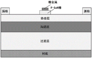
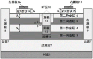
1. a common source type power device comprising from bottom to top: substrate 1, transition layer 2, second channel layer 5 and second barrier layer 6, its characterized in that:
a first channel layer 3 and a first barrier layer 4 are inserted between the transition layer 2 and the second channel layer 5, and the first barrier layer 4 is positioned on the upper part of the first channel layer 3;
the left side and the right side of the first channel layer 3, the first barrier layer 4, the second channel layer 5 and the second barrier layer 6 are respectively provided with a table top 7, the lower ends of the two table tops 7 are respectively positioned at the upper part of the transition layer 2, and the table tops 7 at the left side and the right side are respectively provided with a left drain electrode 8 and a right drain electrode 9;
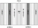
an N + region 10 is arranged in the middle of the second channel layer 5 and the second barrier layer 6, and the lower side of the N + region 10 is positioned in the second channel layer 5;
a groove 11 is arranged between the upper part of the N + region 10 and the interior of the first channel layer 3, a source electrode 13 and an anode electrode 12 are respectively arranged at the upper part and the lower part of the interior of the groove, and the contact surfaces of the two electrodes are positioned at the lower side of the N + region 10;
a left P-type block 14 and a left grid 16 are arranged on the second barrier layer 6 between the left drain electrode 8 and the source electrode 13; and a right P-type block 15 and a right grid 17 are arranged on the second barrier layer 6 between the right drain electrode 9 and the source electrode 13.
Further, the thickness S of the first barrier layer 4 1 2-60 nm, and the thickness S of the second barrier layer 6 2 2 to 60 nm.
Further, the N + region 10 is an N-type heavily doped region with an implantation dose greater than 1 × 10 20 cm -2 。
Further, the lower side of the recess 11 is located inside the first channel layer 3, and the distance between the lower side of the recess 11 and the upper surface of the first channel layer 3 is at least 5 nm.
Further, the distance t between the upper side of the anode 12 and the lower side of the N + region 10 is >0 nm.
Furthermore, the thickness h of the left P-type block 14 and the right P-type block 15 is 10-500 nm, and the doping concentration is 1 multiplied by 10 16 ~5×10 20 cm -3 。
Further, the left gate 16 is located at the upper portion of the left P-type block 14, and the right gate 17 is located at the upper portion of the right P-type block 15.
Further, the left drain electrode 8 and the right drain electrode 9 adopt the same metal combination, and ohmic contact is formed between the left drain electrode and the right drain electrode and a contacted semiconductor;
further, the anode 12 is made of multiple layers of metal, the metal at the bottom layer is a high work function metal, and schottky contact is formed between the anode 12 and a contacted semiconductor;
further, an ohmic contact is formed between the source electrode 13 and the contacted semiconductor.
2. A method for manufacturing the common source type power device is characterized by comprising the following steps:
A) extending a GaN-based wide bandgap semiconductor material on a substrate 1 to form a transition layer 2 with the thickness of 1-50 mu m;
B) manufacturing a channel layer and a barrier layer:
B1) extending a GaN material on the transition layer 2 to form a first channel layer 3 with the thickness of 10-200 nm;
B2) a GaN-based wide bandgap semiconductor material is epitaxially formed on the first channel layer 3 to a thickness S 1 A first barrier layer 4 of 2 to 60 nm;
B3) extending a GaN material on the first barrier layer 4 to form a second channel layer 5 with the thickness of 10-200 nm;
B4) a GaN-based wide bandgap semiconductor material is epitaxially formed on the second channel layer 5to a thickness S 2 A second barrier layer 6 of 2 to 60 nm;
C) manufacturing a mask on the second barrier layer 6 for the first time, etching the two sides of the second barrier layer 6, the second channel layer 5, the first barrier layer 4 and the first channel layer 3 by using the mask respectively until the two sides are etched to the upper surface of the transition layer 2 to form a left table top 7 and a right table top 7;
D) respectively depositing a plurality of layers of metal on the left table-board 7 and the right table-board 7 by using the mask manufactured in the step C), and performing rapid thermal annealing to form a left drain electrode 8 and a right drain electrode 9, wherein ohmic contact is formed between the two drain electrodes and a contacted semiconductor;
E) making masks on the second barrier layer 6, the left drain electrode 8 and the right drain electrode 9 for the second time, and performing ion implantation on the middle positions of the second channel layer 5 and the second barrier layer 6 by using the masks to form an N + region 10, wherein when the implantation dosage and energy are determined, the first channel layer 3 is ensured not to be damaged;
F) a mask is manufactured on the second barrier layer 6, the left drain electrode 8, the right drain electrode 9 and the N + region 10 for the third time, and the middle of the N + region 10, the second channel layer 5, the first barrier layer 4 and the first channel layer 3 are respectively etched by using the mask to form a groove 11;
G) depositing a plurality of layers of metal inside the groove 11 by using the mask manufactured in the step F) to form an anode 12, wherein Schottky contact is formed between the anode 12 and the semiconductor material contacted with the anode; depositing a metal combination on the upper part of the anode 12 to form a source electrode 13, wherein ohmic contact is formed between the source electrode 13 and the second channel layer 5 as well as between the source electrode 13 and the first barrier layer 4;
H) extending a P-type semiconductor material on the second barrier layer 6, the left drain electrode 8, the right drain electrode 9, the N + region 10 and the source electrode 13 to form a P-type layer; making a mask on the P-type layer for the fourth time, and etching the P-type layer by using the mask to form a left P-type block 14 and a right P-type block 15;
I) and (3) making a mask on the second barrier layer 6, the left drain electrode 8, the right drain electrode 9, the N + region 10, the source electrode 13, the left P-type block 14 and the right P-type block 15 for the fifth time, depositing multiple layers of metal on the left P-type block 14 and the right P-type block 15 by using the mask to form a left grid electrode 16 and a right grid electrode 17 respectively, and finishing the manufacture of the whole device.
Compared with the traditional gallium nitride-based enhanced switch device, the device has the following advantages:
first, bidirectional conduction and bidirectional blocking characteristics can be realized.
The device is inserted with a first channel layer and a first barrier layer, the contact interface of the channel layer and the first barrier layer forms an electronic channel, the channel, a left drain electrode and an anode form a left Schottky diode structure, the channel, a right drain electrode and an anode form a right Schottky diode structure, and the two diodes are distributed back to back, so that electrons have a leftward current path in the left Schottky diode and a rightward current path in the right Schottky diode;
meanwhile, due to the combined action of spontaneous polarization and piezoelectric polarization, a two-dimensional electron gas channel is formed at the contact interface of the second channel layer and the second barrier layer, the channel, the left drain electrode, the source electrode, the left P-type block and the left grid electrode form a left switch transistor, the channel, the right drain electrode, the source electrode, the right P-type block and the right grid electrode form a right switch transistor, namely the two transistors are connected through sharing the source electrode, so that electrons have a right current path in the left transistor and a left current path in the right transistor, the on and off of the left transistor and the right transistor can be changed by controlling the potentials on the left grid electrode and the right grid electrode, meanwhile, the states of two diodes are controlled by applying different voltages to the left drain electrode and the right drain electrode, and the bidirectional conduction characteristic and the bidirectional blocking characteristic of the device are realized at the same time.
Secondly, the device adopts a mode of vertically stacking the switch transistor and the Schottky diode, and compared with the traditional mode of placing discrete components on the same PCB for interconnection, the device can reduce parasitic parameters caused by interconnection and obviously improve the integration level of the switch device.
Thirdly, the active region between the drain electrode and the source electrode of the switch transistor is superposed with the active region between the anode electrode and the drain electrode of the Schottky diode in the vertical direction, the drain electrode is used as the cathode of the diode and the drain electrode of the switch transistor, two back-to-back diodes share the anode electrode, the two transistors share the source electrode, external connection is reduced, and the area of the device in the horizontal direction is greatly reduced.
Fourthly, because the device of the invention adopts two embedded Schottky diodes, when the device works in a diode unidirectional conduction mode, very low starting voltage can be realized.
Detailed Description
Embodiments of the present invention are described in further detail below with reference to the accompanying drawings.
Referring to fig. 2 and 3, the common source type power device of the present invention includes: the structure comprises a substrate 1, a transition layer 2, a barrier layer 3, a first barrier layer 4, a second channel layer 5, a second barrier layer 6, a table-board 7, a left drain electrode 8, a right drain electrode 9, an N + region 10, a groove 11, an anode 12, a source electrode 13, a left P-type block 14, a right P-type block 15, a left grid electrode 16 and a right grid electrode 17. Wherein:
the substrate 1 is made of silicon carbide or sapphire or silicon or other materials;
the transition layer 2 is positioned at the upper part of the substrate 1 and is composed of a plurality of layers of same or different GaN-based wide bandgap semiconductor materials, and the thickness of the transition layer is 1-50 mu m;
the first channel layer 3 is located on the upper portion of the transition layer 2, is made of GaN materials, and is 10-200 nm thick;
the first barrier layer 4 is located on the first channel layer 3, and is made of GaN-based wide bandgap semiconductor material with a thickness S 1 2-60 nm;
the second channel layer 5 is located on the first barrier layer 4, is made of GaN materials, and has a thickness of 10-200 nm;
the second barrier layer 6 is arranged on the second channel layer 5 and is made of GaN-based wide bandgap semiconductor material with a thickness S 2 2-60 nm;
the two mesas 7 are respectively positioned on the left side and the right side of the first channel layer 3, the first barrier layer 4, the second channel layer 5 and the second barrier layer 6, and the lower ends of the two mesas 7 are positioned on the upper part of the transition layer 2;
the left drain electrode 8 and the right drain electrode 9 are respectively positioned on the upper parts of the table tops 7 on the left side and the right side, are combined by adopting the same multilayer metal, and form ohmic contact with a contacted semiconductor;
the N + region 10 is located in the middle of the second channel layer 5 and the second barrier layer 6, the lower side of the N + region is located in the second channel layer 5, the N + region 10 is an N-type heavily doped region formed by ion implantation, and the implantation dosage is greater than 1 × 10 20 cm -2 And when the implantation depth and the dosage are selected, the first channel layer 3 is ensured to be almost free of damage;
the groove 11 is positioned between the upper part of the N + region 10 and the inside of the first channel layer 3, the lower side of the groove 11 is positioned in the first channel layer 3, and the distance between the lower side of the groove 11 and the upper surface of the first channel layer 3 is at least 5 nm;
the anode 12 is positioned in the groove 11, the distance t between the upper part of the anode 12 and the lower part of the N + region 10 is greater than 0nm, the anode 12 is formed by combining multiple layers of metals, the metal at the bottommost layer is a high-work-function metal, and Schottky contact is formed between the anode 12 and a contacted semiconductor;
the source electrode 13 is positioned on the upper part of the anode 12, the contact surface of the source electrode 13 and the anode 12 is positioned on the lower side of the N + region 10, and the source electrode 13 and a contacted semiconductor form ohmic contact;
the left P-shaped block 14 is positioned on the second barrier layer 6 between the left drain electrode 8 and the source electrode 13, the right P-shaped block 15 is positioned on the second barrier layer 6 between the right drain electrode 9 and the source electrode 13, the thicknesses h of the left P-shaped block 14 and the right P-shaped block 15 are both 10-500 nm, and the doping concentrations are both 1 multiplied by 10 16 ~5×10 20 cm -3 When determining the thickness h of the left P-type block 14 and the right P-type block 15, ensuring that the thicknesses have almost no depletion effect on the first barrier layer 4;
the left gate 16 is located on the top of the left P-block 14 and the right gate 17 is located on the top of the right P-block 15.
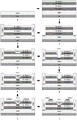
Referring to fig. 4, the common source type power device manufactured by the present invention shows the following three embodiments.
The first embodiment is as follows: the first channel layer 3, the first barrier layer 4, the second channel layer 5 and the second barrier layer 6 are respectively manufactured on the silicon carbide substrate, the thicknesses of the first channel layer, the first barrier layer, the second barrier layer and the second barrier layer are respectively 10nm, 2nm, 10nm and 2nm, and the implantation dosage of the N + region 10 is 5 multiplied by 10 20 cm -2 The distance t between the lower part of the N + region 10 and the upper part of the anode 12 is 1nm, the thickness h of the left P-type block 14 and the right P-type block 15 are both 10nm, and the doping concentration is 5 multiplied by 10 18 cm -3 The common source type power device of (1).
Step 1, epitaxial growth of AlN and GaN materials on a silicon carbide substrate 1 from bottom to top to form a transition layer 2, as shown in FIG. 4 a.
(1.1) extending an undoped AlN material with the thickness of 100nm on the silicon carbide substrate 1 by using a metal organic chemical vapor deposition technology, wherein the process conditions of the metal organic chemical vapor deposition are as follows: the temperature is 1000 ℃, the pressure is 45Torr, the hydrogen flow is 4400sccm, the ammonia flow is 4400sccm, and the aluminum source flow is 5 mu mol/min;
(1.2) using a metal organic chemical vapor deposition technology to epitaxially grow a GaN material with the thickness of 0.9 mu m on the AlN material to finish the manufacture of the transition layer 2, wherein the process conditions are as follows: the temperature was 960 deg.C, the pressure was 45Torr, the hydrogen flow was 4400sccm, the ammonia flow was 4400sccm, and the gallium source flow was 120. mu. mol/min.
And 2, manufacturing a channel layer and a barrier layer on the GaN transition layer 2, as shown in FIG. 4 b.
(2.1) extending a GaN material on the GaN transition layer 2 by using a metal organic chemical vapor deposition technology to form a first channel layer 3 with the thickness of 10 nm; the process conditions of the metal organic chemical vapor deposition are as follows: the temperature is 900 ℃, the pressure is 40Torr, the hydrogen flow is 4000sccm, the ammonia flow is 4000sccm, and the gallium source flow is 90 mu mol/min;
(2.2) epitaxial thickness S on the first channel layer 3 using a metal organic chemical vapor deposition technique 1 Undoped Al of 2nm and an aluminum component of 0.4 0.4 Ga 0.6 N, forming a first barrier layer 4; the process conditions are as follows: the temperature is 980 ℃, the pressure is 45Torr, the hydrogen flow is 4300sccm, the ammonia flow is 4300sccm, the gallium source flow is 35 mu mol/min, and the aluminum source flow is 7 mu mol/min;
(2.3) extending a GaN material on the first barrier layer 4 by using a metal organic chemical vapor deposition technology to form a second channel layer 5 with the thickness of 10 nm; the process conditions are as follows: the temperature is 900 ℃, the pressure is 40Torr, the hydrogen flow is 4000sccm, the ammonia flow is 4000sccm, and the gallium source flow is 90 mu mol/min;
(2.4) epitaxial thickness S on the second channel layer 5 using a Metal organic chemical vapor deposition technique 2 Undoped Al of 2nm and an aluminum component of 0.3 0.3 Ga 0.7 N, forming a second barrier layer 6; the process conditions are as follows: the temperature was 980 ℃, the pressure was 45Torr, the hydrogen flow was 4200sccm, the ammonia flow was 4200sccm, the gallium source flow was 39. mu. mol/min, and the aluminum source flow was 5. mu. mol/min.
And step 3, manufacturing the table top 7 as shown in fig. 4 c.
Manufacturing a mask on the second barrier layer 6 for the first time, respectively etching the two sides of the second barrier layer 6, the second channel layer 5, the first barrier layer 4 and the first channel layer 3 by utilizing the mask through a reactive ion etching technology until the two sides are etched to the upper surface of the transition layer 2 to form a left table board 7 and a right table board 7;
the etching adopts the following process conditions: cl 2 The flow rate is 15sccm, the pressure is 10mTorr, and the power is 100W.
And 4, depositing to form a left drain electrode 8 and a right drain electrode 9, as shown in FIG. 4 d.
Respectively depositing a plurality of layers of metals on the left table-board 7 and the right table-board 7 by using an electron beam evaporation technology by using the mask manufactured in the step 3, wherein the plurality of layers of metals are Al, Ni and Au, the thicknesses of the plurality of layers of metals are respectively 0.016 mu m/0.177 mu m/0.058 mu m, and the N is heated at 870 ℃ under the condition that the N is heated 2 Performing rapid thermal annealing for 30s in the atmosphere to form a left drain electrode 8 and a right drain electrode 9, wherein ohmic contact is formed between the two drain electrodes and the contacted semiconductor;
the deposition process conditions are as follows: vacuum degree less than 1.8X 10
-3 Pa, power of 380W, evaporation rate of less than
Step 5, manufacturing the N + region 10, as shown in fig. 4 e.
Making masks on the second barrier layer 6, the left drain electrode 8 and the right drain electrode 9 for the second time, and performing ion implantation on the middle positions of the second channel layer 5 and the second barrier layer 6 by using the masks to form an N + region 10;
the process conditions of ion implantation are as follows: the implanted N-type impurity is nitrogen ion, the implantation energy is 17keV, and the implantation dosage is 5 × 10 20 cm -2 。
Step 6, etching to form a groove 11, as shown in fig. 4 f.
A mask is manufactured on the second barrier layer 6, the left drain electrode 8, the right drain electrode 9 and the N + region 10 for the third time, the middle part of the N + region 10, the second channel layer 5, the first barrier layer 4 and the first channel layer 3 are respectively etched by utilizing the mask and using a reactive ion etching technology, the etching depth is 19nm, and a groove 11 is formed;
the process conditions for etching the groove are as follows: cl 2 The flow rate is 15sccm, the pressure is 10mTorr, and the power is 100W.
And 7, manufacturing an anode 12 in the groove 11, as shown in fig. 4 g.
Depositing a plurality of layers of metal inside the groove 11 by using the mask manufactured in the step 6 and using an electron beam evaporation technology, wherein the deposited metal is a Ti/Au metal combination, namely the lower layer is Ti, the upper layer is Au, the thickness of the metal is 0.004 mu m/0.002 mu m, an anode 12 is formed, and Schottky contact is formed between the anode 12 and the contacted semiconductor material;
the process conditions adopted for depositing the metal are as follows: vacuum degree less than 1.8X 10
-3 Pa, power of 200W, evaporation rate of less than
And 8, manufacturing a source electrode 13 on the anode 12, as shown in fig. 4 h.
Depositing a plurality of layers of metal Al, Ni and Au with the thickness of 0.008 [ mu ] m/0.005 [ mu ] m/0.006 [ mu ] m on the upper part of the anode 12 by using the mask manufactured in the step 6 by using an electron beam evaporation technology to form a source electrode 13, wherein ohmic contact is formed among the source electrode 13, the second channel layer 5 and the first barrier layer 4;
the process conditions adopted for depositing the metal are as follows: vacuum degree less than 1.8X 10
-3 Pa, power of 400W, evaporation rate of less than
And 9, manufacturing a left P-type block 14 and a right P-type block 15 as shown in FIG. 4 i.
(9.1) Using magnetron sputtering technique, the doping concentration is 5 × 10 epitaxially on the second barrier layer 6, the left drain electrode 8, the right drain electrode 9, the N + region 10 and the source electrode 13 18 cm -3 Forming a P-type NiO layer by using a NiO material with the thickness of 10 nm;
the sputtering process conditions are as follows: the power is 110W, the temperature is 300 ℃, the Ar flow is 20sccm, O 2 The flow rate is 30 sccm;
(9.2) manufacturing a mask on the P-type NiO layer for the fourth time, etching the P-type NiO layer by using the mask and using a reactive ion etching technology until the upper surface of the second barrier layer 6 is etched, and respectively forming a left P-type block 14 and a right P-type block 15;
the etching process conditions are as follows: cl 2 The flow rate is 15sccm, the pressure is 10mTorr, and the power is 120W.
Step 10, manufacturing a left gate 16 and a right gate 17, as shown in fig. 4 j.
Making a mask on the second barrier layer 6, the left drain electrode 8, the right drain electrode 9, the N + region 10, the source electrode 13, the left P-type block 14 and the right P-type block 15 for the fifth time, and respectively depositing metal combinations Ta/Au on the left P-type block 14 and the right P-type block 15 by utilizing the mask by using a sputtering technology, wherein the lower layer is Ta, the upper layer is Au, and the thicknesses of the Ta/Au combinations are respectively 0.021 mu m/0.28 mu m; and respectively forming a left grid 16 and a right grid 17 to finish the manufacture of the whole device.
The sputtering process conditions are as follows: the air pressure is about 0.1Pa, the flow rate of Ar is 8sccm, the substrate temperature is fixed at 200 ℃, and the target radio frequency power is 150W.
Example two: the first channel layer 3, the first barrier layer 4, the second channel layer 5 and the second barrier layer 6 are respectively manufactured on a sapphire substrate with the thicknesses of 200nm, 60nm, 200nm and 60nm, and the implantation dosage of the N + region 10 is 2 multiplied by 10 21 cm -2 The distance t between the lower part of the N + region 10 and the upper part of the anode 12 is 20nm, the thickness h of the left P-type block 14 and the right P-type block 15 are both 500nm, and the doping concentration is 1 multiplied by 10 16 cm -3 The common source type power device of (1).
Step one, a transition layer 2 is made on a sapphire substrate 1 through epitaxial growth of a GaN material, as shown in FIG. 4 a.
A transition layer 2 is formed by extending a GaN material with a thickness of 50 μm on a sapphire substrate 1 by using a metal organic chemical vapor deposition technology under the process conditions that the temperature is 980 ℃, the pressure is 47Torr, the hydrogen flow is 4400sccm, the ammonia flow is 4400sccm, and the gallium source flow is 120 μmol/min.
Step two, manufacturing a channel layer and a barrier layer on the GaN transition layer 2, as shown in FIG. 4 b.
(2a) Extending a GaN material on the GaN transition layer 2 by using a metal organic chemical vapor deposition technology under the process conditions that the temperature is 900 ℃, the pressure is 40Torr, the hydrogen flow is 4000sccm, the ammonia flow is 4000sccm and the gallium source flow is 90 mu mol/min to form a first channel layer 3 with the thickness of 200 nm;
(2b) using metal organic chemical vapor deposition technology to extend the thickness S on the first channel layer 3 under the process conditions that the temperature is 980 ℃, the pressure is 45Torr, the hydrogen flow is 4300sccm, the ammonia flow is 4300sccm, the gallium source flow is 35 mu mol/min and the aluminum source flow is 7 mu mol/min 1 60nm and an aluminum component of 0.2 0.2 Ga 0.8 N, forming a first barrier layer 4;
(2c) extending a GaN material on the first barrier layer 4 by using a metal organic chemical vapor deposition technology under the process conditions of the temperature of 900 ℃, the pressure of 40Torr, the hydrogen flow of 4000sccm, the ammonia flow of 4000sccm and the gallium source flow of 90 mu mol/min to form a second channel layer 5 with the thickness of 200 nm;
(2d) using metal organic chemical vapor deposition technology to perform epitaxial thickness S on the second channel layer 5 under the process conditions that the temperature is 980 ℃, the pressure is 45Torr, the hydrogen flow is 4200sccm, the ammonia flow is 4200sccm, the gallium source flow is 39 mu mol/min and the aluminum source flow is 5 mu mol/min 2 60nm and an aluminum component of 0.1 0.1 Ga 0.9 N, forming a second barrier layer 6.
Step three, manufacturing the table-board 7 as shown in fig. 4 c.
A first mask is made on the second barrier layer 6, with which a reactive ion etching technique is used in Cl 2 Under the process conditions of 15sccm flow, 10mTorr pressure and 100W power, the two sides of the second barrier layer 6, the second channel layer 5, the first barrier layer 4 and the first channel layer 3 are respectively etched until the upper surface of the transition layer 2, so as to form a left table board 7 and a right table board 7.
Step four, depositing to form a left drain electrode 8 and a right drain electrode 9, as shown in fig. 4 d.
Using the mask made in the third step, the vacuum degree is less than 1.8 multiplied by 10
-3 Pa, power of 380W, evaporation rate of less than
Respectively depositing a multilayer metal combination on the left table-board 7 and the right table-board 7 by using an electron beam evaporation technology, wherein the multilayer metal adopts Ti, Al, Ni and Au, the thicknesses of the multilayer metal are respectively 0.226 mu m/0.216 mu m/0.177 mu m/0.158 mu m, and N is 870 ℃ at the temperature
2 And performing rapid thermal annealing for 30s in the atmosphere to form a
left drain electrode 8 and a right drain electrode 9, wherein ohmic contact is formed between the two drain electrodes and the contacted semiconductor.
Step five, manufacturing the N + region 10, as shown in FIG. 4 e.
Making a mask on the second barrier layer 6, the left drain electrode 8 and the right drain electrode 9 for the second time, and using the mask to implant 2 × 10 doses at an implantation energy of 17keV 21 cm -2 Under the process conditions of (1), an N-type impurity, which is phosphorus ions, is implanted into the intermediate positions of the second channel layer 5 and the second barrier layer 6, thereby forming an N + region 10.
Step six, forming a groove 11 by etching, as shown in fig. 4 f.
Making a mask on the second barrier layer 6, the left drain electrode 8, the right drain electrode 9 and the N + region 10 for the third time, and using the mask to perform reactive ion etching on Cl 2 Under the process conditions of 15sccm flow, 10mTorr pressure and 100W power, the middle part of the N + region 10, the second channel layer 5, the first barrier layer 4 and the first channel layer 3 are respectively etched, the etching depth is 340nm, and a groove 11 is formed.
Step seven, manufacturing an anode 12 in the groove 11, as shown in fig. 4 g.
Utilizing the mask made in the sixth step, and utilizing electron beam evaporation technology to make vacuum degree be less than 1.8X 10
-3 Pa, power of 200W, evaporation rate of less than
Under the process conditions of (1), depositing a plurality of layers of metal inside the groove 11, wherein the deposited metal is a W/Au metal combination, namely the lower layer is W, the upper layer is Au, the thickness of the deposited metal is 0.035 μm/0.015 μm, and an
anode 12 is formed, and Schottky contact is formed between the
anode 12 and the contacted semiconductor material.
And step eight, manufacturing a source electrode 13 on the upper part of the anode 12, as shown in figure 4 h.
Reusing the mask made in the sixth step, and keeping the vacuum degree less than 1.8 multiplied by 10
-3 Pa, power of 400W, evaporation rate of less than
Under the process conditions of (1), a plurality of layers of metals of Ti, Al, Ni and Au are deposited on the upper part of the
anode 12 by using an electron beam evaporation technology, the thicknesses of the metals are respectively 0.059/0.068 mu m/0.185 mu m/0.076 mu m, a
source electrode 13 is formed, and ohmic contact is formed between the
source electrode 13 and the second channel layer 5 and the
first barrier layer 4.
And step nine, manufacturing a left P-type block 14 and a right P-type block 15, as shown in FIG. 4 i.
(9a) Using metal organic chemical vapor deposition technology, under the process conditions that the temperature is 950 ℃, the pressure is 40Torr, the hydrogen flow is 4000sccm, a high-purity Mg source is taken as a doping agent, the ammonia flow is 4000sccm, and the gallium source flow is 100 mu mol/min, the epitaxial doping concentration on the second barrier layer 6, the left drain electrode 8, the right drain electrode 9, the N + region 10 and the source electrode 13 is 1 multiplied by 10 16 cm -3 Forming a P-type GaN layer by using a P-type GaN material with the thickness of 500 nm;
(9b) making a mask on the P-type GaN layer for the fourth time, and coating Cl on the mask 2 Etching the P-type GaN layer by using a reactive ion etching technology under the process conditions of 15sccm of flow, 10mTorr of pressure and 120W of power until the upper surface of the second barrier layer 6, and respectively forming a left P-type block 14 and a right P-type block 15.
Step ten, manufacturing the left grid 16 and the right grid 17, as shown in fig. 4 j.
Making masks on the second barrier layer 6, the left drain electrode 8, the right drain electrode 9, the N + region 10, the source electrode 13, the left P-type block 14 and the right P-type block 15 for the fifth time, and respectively depositing metal combination Gd/Au on the left P-type block 14 and the right P-type block 15 by utilizing the masks by using a sputtering technology under the process conditions that the air pressure is about 0.1Pa, the flow rate of Ar is 8sccm, the temperature of the substrate is fixed at 200 ℃ and the target radio frequency power is 150W, namely the lower layer is Gd, the upper layer is Au, and the thicknesses of the Gd and the Au are respectively 0.021 mu m/0.28 mu m; and respectively forming a left grid 16 and a right grid 17 to finish the manufacture of the whole device.
Example three: fabricating a first on a silicon substrateThe thicknesses of the channel layer 3, the first barrier layer 4, the second channel layer 5 and the second barrier layer 6 are respectively 40nm, 35nm, 70nm and 20nm, and the implantation dosage of the N + region 10 is 4 multiplied by 10 22 cm -2 The distance t between the lower part of the N + region 10 and the upper part of the anode 12 is 40nm, the thicknesses h of the left P-type block 14 and the right P-type block 15 are both 120nm, and the doping concentration is 5 multiplied by 10 20 cm -3 The common source type power device of (1).
Step A. epitaxial growth of AlN and GaN materials on a silicon substrate 1 from bottom to top to form a transition layer 2, as shown in FIG. 5 a.
(A1) Setting the process conditions of 800 ℃, 40Torr of pressure, 4000sccm of hydrogen flow, 4000sccm of ammonia flow and 25 mu mol/min of aluminum source flow, and extending AlN material with the thickness of 400nm on the silicon substrate 1 by using a metal organic chemical vapor deposition technology;
(A2) setting the process conditions of 980 ℃, 45Torr of pressure, 4000sccm of hydrogen flow, 4000sccm of ammonia flow and 120 mu mol/min of gallium source flow, and using a metal organic chemical vapor deposition technology to epitaxially grow a GaN material with a thickness of 5.6 mu m on the AlN material to complete the manufacture of the transition layer 2.
And B, manufacturing a channel layer and a barrier layer on the GaN transition layer 2, as shown in figure 4 b.
(B1) Setting the technological conditions of 900 ℃ of temperature, 40Torr of pressure, 4000sccm of hydrogen flow, 4000sccm of ammonia flow and 90 mu mol/min of gallium source flow, and extending a GaN material on the GaN transition layer 2 by using a metal organic chemical vapor deposition technology to form a first channel layer 3 with the thickness of 40 nm;
(B2) setting the technological conditions of 980 deg.C, 45Torr pressure, 4300sccm hydrogen flow, 4300sccm ammonia flow, 35 mu mol/min gallium source flow and 7 mu mol/min aluminum source flow, and using metal organic chemical vapor deposition to form an epitaxial thickness S on the first channel layer 3 1 35nm and an aluminum component of 0.25 0.25 Ga 0.75 N, forming a first barrier layer 4;
(B3) setting the process conditions of 900 ℃, 40Torr of pressure, 4000sccm of hydrogen flow, 4000sccm of ammonia flow and 90 mu mol/min of gallium source flow, and extending GaN material on the first barrier layer 4 by using a metal organic chemical vapor deposition technology to form a second channel layer 5 with the thickness of 70 nm;
(B4) setting the process conditions of 980 ℃, 45Torr, 4200sccm of hydrogen flow, 4200sccm of ammonia flow, 39 mu mol/min of gallium source flow and 5 mu mol/min of aluminum source flow, and using the metal organic chemical vapor deposition technology to epitaxially form a thickness S on the second channel layer 5 2 20nm and an aluminum component of 0.3 0.3 Ga 0.7 N, forming a second barrier layer 6.
Step c, the mesa 7 is fabricated as shown in fig. 4 c.
Setting up Cl 2 And etching process conditions of 15sccm flow, 10mTorr pressure and 100W power, manufacturing a mask on the second barrier layer 6 for the first time, respectively etching the two sides of the second barrier layer 6, the second channel layer 5, the first barrier layer 4 and the first channel layer 3 by utilizing the mask by using a reactive ion etching technology until the upper surface of the transition layer 2, and forming a left table board 7 and a right table board 7.
Step d, depositing to form the left drain electrode 8 and the right drain electrode 9, as shown in fig. 4 d.
Setting the vacuum degree to be less than 1.8 multiplied by 10
-3 Pa, power of 380W, evaporation rate of less than
The deposition process conditions of (1) respectively depositing a plurality of layers of metals on the left table-board 7 and the right table-board 7 by using the mask made in the step (C) and adopting an electron beam evaporation technology, wherein the plurality of layers of metals adopt Ta, Ni and Au, the thicknesses of the plurality of layers of metals are respectively 0.016 mu m/0.177 mu m/0.058 mu m, and the N is at 870 DEG C
2 And performing rapid thermal annealing for 30s in the atmosphere to form a
left drain electrode 8 and a right drain electrode 9, wherein ohmic contact is formed between the two drain electrodes and the contacted semiconductor.
Step e. make N + region 10, as shown in fig. 4 e.
The process conditions for ion implantation are set as follows: the implanted N-type impurity is arsenic ion, the implantation energy is 19keV, and the implantation dosage is 4 × 10 22 cm -2 Making a mask on the second barrier layer 6, the left drain electrode 8 and the right drain electrode 9 for the second time, and using the mask to form a second barrier layerIon implantation is performed at the middle position of the two barrier layers 6 to form an N + region 10.
Step f. etch to form a recess 11, as shown in fig. 4 f.
The process conditions of etching are set as follows: cl 2 The flow is 15sccm, the pressure is 10mTorr, the power is 100W, a mask is manufactured on the second barrier layer 6, the left drain electrode 8, the right drain electrode 9 and the N + region 10 for the third time, the middle of the N + region 10, the second channel layer 5, the first barrier layer 4 and the first channel layer 3 are respectively etched by utilizing the mask and using a reactive ion etching technology, the etching depth is 150nm, and the groove 11 is formed.
Step g. anode 12 is made in the groove 11, as shown in fig. 4 g.
The process conditions adopted for depositing the metal are as follows: vacuum degree less than 1.8X 10
-3 Pa, power of 200W, evaporation rate of less than
And F, depositing multiple layers of metal inside the groove 11 by using an electron beam evaporation technology by using the mask manufactured in the step F, wherein the deposited metal is a Ni/Au metal combination, namely the lower layer is Ni, the upper layer is Au, the thicknesses of the deposited metal and the Au are respectively 0.015 mu m/0.015 mu m, and an
anode 12 is formed, and Schottky contact is formed between the
anode 12 and the contacted semiconductor material.
Step H, setting the vacuum degree to be less than 1.8 multiplied by 10
-3 Pa, power of 400W, evaporation rate of less than
Using the mask made in step F again, a plurality of layers of metal Ta, Ni, Au with a thickness of 0.018 μm/0.135 μm/0.046 μm, respectively, are deposited on the upper part of the
anode 12 using electron beam evaporation technique to form a
source electrode 13, which forms an ohmic contact between the
source electrode 13 and the contacting semiconductor, as shown in fig. 4 h.
Step i, making the left P-type block 14 and the right P-type block 15, as shown in fig. 4 i.
(I1) Setting the target material as copper with the purity of 99.999 percent, high-purity argon as sputtering gas, high-purity oxygen with the same purity as reaction gas, and setting the vacuum degree of a reaction chamber before sputtering to be 2.0 multiplied by 10 -4 Pa, sputtering ofThe Ar gas flow rate is kept at 20sccm and O during the injection 2 The flow rate is 10sccm, the pressure of the deposition chamber is 0.5Pa, the RF power is 35W, the substrate temperature is 200 ℃, and the magnetron sputtering technique is used to epitaxially dope the second barrier layer 6, the left drain electrode 8, the right drain electrode 9, the N + region 10 and the source electrode 13 with a concentration of 5 × 10 20 cm -3 Forming a P-type CuO layer by using a CuO material with the thickness of 120 nm;
(I2) setting up Cl 2 And etching the P-type CuO layer by using the mask and a reactive ion etching technology until the upper surface of the second barrier layer 6 under the etching process conditions of 15sccm, 10mTorr and 120W of power, so as to form a left P-type block 14 and a right P-type block 15 respectively.
Step j. make left gate 16 and right gate 17, as shown in fig. 4 j.
The sputtering process conditions are set as follows: the air pressure is about 0.1Pa, the flow rate of Ar is 8sccm, the substrate temperature is fixed at 200 ℃, the target radio frequency power is 150W, masks are manufactured on the second barrier layer 6, the left drain electrode 8, the right drain electrode 9, the N + region 10, the source electrode 13, the left P-type block 14 and the right P-type block 15 for the fifth time, and metal combinations with Ta as the lower layer and Ni as the upper layer are respectively deposited on the left P-type block 14 and the right P-type block 15 by utilizing the masks and using the sputtering technology, wherein the thicknesses of the metal combinations are respectively 0.021 mu m/0.28 mu m; and respectively forming a left grid 16 and a right grid 17 to finish the manufacture of the whole device.
The effects of the present invention can be further illustrated by the following test results.
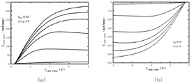
Testing one: the device of the second embodiment of the present invention is subjected to a conduction test, and the result is shown in fig. 5, where: fig. 5(a) shows the result of the forward conduction test, and fig. 5(b) shows the result of the reverse conduction test, and it can be seen from fig. 5 that the device of the present invention has excellent bidirectional conduction characteristics;
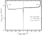
and (2) testing: the result of the blocking test performed on the device in the second embodiment of the present invention is shown in fig. 6, and as can be seen from fig. 6, the device in the present invention can implement bidirectional blocking, and forward and reverse off-state breakdown voltages are 861V and-822V, respectively, which indicates that the device in the present invention has excellent bidirectional conduction and bidirectional blocking characteristics.
The foregoing description is only three specific embodiments of the present invention and is not intended to limit the present invention, and it will be apparent to those skilled in the art that various modifications and variations in form and detail can be made in the method according to the present invention without departing from the principle and scope of the invention, but these modifications and variations are within the scope of the invention as defined in the appended claims.