CN111257713A - A method for measuring multiple lifetimes of carriers in semiconductor materials with multiple luminescence peaks - Google Patents
A method for measuring multiple lifetimes of carriers in semiconductor materials with multiple luminescence peaks Download PDFInfo
- Publication number
- CN111257713A CN111257713A CN201911352634.2A CN201911352634A CN111257713A CN 111257713 A CN111257713 A CN 111257713A CN 201911352634 A CN201911352634 A CN 201911352634A CN 111257713 A CN111257713 A CN 111257713A
- Authority
- CN
- China
- Prior art keywords
- photoluminescence
- signal
- frequency
- semiconductor material
- carriers
- Prior art date
- Legal status (The legal status is an assumption and is not a legal conclusion. Google has not performed a legal analysis and makes no representation as to the accuracy of the status listed.)
- Pending
Links
- 238000000034 method Methods 0.000 title claims abstract description 49
- 239000004065 semiconductor Substances 0.000 title claims abstract description 43
- 239000000463 material Substances 0.000 title claims abstract description 30
- 239000000969 carrier Substances 0.000 title claims abstract description 24
- 238000004020 luminiscence type Methods 0.000 title abstract description 20
- 238000005259 measurement Methods 0.000 claims abstract description 25
- 238000005424 photoluminescence Methods 0.000 claims abstract description 25
- 230000005284 excitation Effects 0.000 claims abstract description 16
- 230000005855 radiation Effects 0.000 claims abstract description 15
- 238000000103 photoluminescence spectrum Methods 0.000 claims abstract description 9
- 230000003287 optical effect Effects 0.000 claims description 10
- 238000001228 spectrum Methods 0.000 claims description 5
- 238000001748 luminescence spectrum Methods 0.000 claims description 4
- 238000012545 processing Methods 0.000 claims description 4
- 230000003595 spectral effect Effects 0.000 claims description 4
- 238000004458 analytical method Methods 0.000 claims description 3
- 238000007405 data analysis Methods 0.000 claims description 3
- 238000002474 experimental method Methods 0.000 claims description 3
- 230000010354 integration Effects 0.000 claims description 3
- 238000004364 calculation method Methods 0.000 claims description 2
- 238000012795 verification Methods 0.000 claims description 2
- 238000013329 compounding Methods 0.000 claims 1
- 238000012360 testing method Methods 0.000 abstract description 17
- 238000001514 detection method Methods 0.000 abstract description 3
- 239000000523 sample Substances 0.000 description 27
- 238000005516 engineering process Methods 0.000 description 5
- 239000002210 silicon-based material Substances 0.000 description 4
- 238000002347 injection Methods 0.000 description 3
- 239000007924 injection Substances 0.000 description 3
- 239000000243 solution Substances 0.000 description 3
- 238000010521 absorption reaction Methods 0.000 description 2
- 238000009792 diffusion process Methods 0.000 description 2
- 238000000691 measurement method Methods 0.000 description 2
- 238000005215 recombination Methods 0.000 description 2
- 230000006798 recombination Effects 0.000 description 2
- 238000010998 test method Methods 0.000 description 2
- 230000003321 amplification Effects 0.000 description 1
- 238000012512 characterization method Methods 0.000 description 1
- 230000001066 destructive effect Effects 0.000 description 1
- 238000010586 diagram Methods 0.000 description 1
- 239000011521 glass Substances 0.000 description 1
- 238000003384 imaging method Methods 0.000 description 1
- 238000003199 nucleic acid amplification method Methods 0.000 description 1
- 239000002245 particle Substances 0.000 description 1
- 238000000628 photoluminescence spectroscopy Methods 0.000 description 1
- 239000002096 quantum dot Substances 0.000 description 1
- 238000002310 reflectometry Methods 0.000 description 1
- 238000011160 research Methods 0.000 description 1
- 238000004528 spin coating Methods 0.000 description 1
- 230000001052 transient effect Effects 0.000 description 1
Images
Classifications
-
- G—PHYSICS
- G01—MEASURING; TESTING
- G01R—MEASURING ELECTRIC VARIABLES; MEASURING MAGNETIC VARIABLES
- G01R31/00—Arrangements for testing electric properties; Arrangements for locating electric faults; Arrangements for electrical testing characterised by what is being tested not provided for elsewhere
- G01R31/26—Testing of individual semiconductor devices
- G01R31/2642—Testing semiconductor operation lifetime or reliability, e.g. by accelerated life tests
-
- G—PHYSICS
- G01—MEASURING; TESTING
- G01R—MEASURING ELECTRIC VARIABLES; MEASURING MAGNETIC VARIABLES
- G01R31/00—Arrangements for testing electric properties; Arrangements for locating electric faults; Arrangements for electrical testing characterised by what is being tested not provided for elsewhere
- G01R31/26—Testing of individual semiconductor devices
- G01R31/2601—Apparatus or methods therefor
-
- G—PHYSICS
- G01—MEASURING; TESTING
- G01R—MEASURING ELECTRIC VARIABLES; MEASURING MAGNETIC VARIABLES
- G01R31/00—Arrangements for testing electric properties; Arrangements for locating electric faults; Arrangements for electrical testing characterised by what is being tested not provided for elsewhere
- G01R31/26—Testing of individual semiconductor devices
- G01R31/2648—Characterising semiconductor materials
Landscapes
- Physics & Mathematics (AREA)
- General Physics & Mathematics (AREA)
- Investigating, Analyzing Materials By Fluorescence Or Luminescence (AREA)
- Testing Or Measuring Of Semiconductors Or The Like (AREA)
Abstract
本发明涉及一种用于测量多发光峰半导体材料中载流子多重寿命的方法,其中:测试系统由光载流子辐射测量系统和光致发光光谱测量系统综合组成;一束光子能量大于待测半导体禁带宽度的并以方波信号调制的激光作为激励光,经透镜聚焦照射到待测半导体材料表面,激发出相同周期的光致发光信号;在该方法中通过改变激励光频率和探测波长,得到不同条件下光致发光信号的幅值及相位与激励频率的关系,再通过建立信号与寿命相关的物理模型,经数据拟合计算得出载流子的有效寿命和多重寿命分量;通过综合分析不同实验条件下的测量结果,分析得到更准确地载流子多重寿命分布情况。
The invention relates to a method for measuring the multiple lifetimes of carriers in a semiconductor material with multiple luminescence peaks, wherein: a test system is composed of a photocarrier radiation measurement system and a photoluminescence spectrum measurement system; A laser with a semiconductor band gap and modulated by a square wave signal is used as excitation light, which is focused and irradiated to the surface of the semiconductor material to be measured through a lens, and a photoluminescence signal of the same period is excited; in this method, the frequency of excitation light and detection wavelength are changed by changing. , obtain the relationship between the amplitude and phase of the photoluminescence signal and the excitation frequency under different conditions, and then establish a physical model related to the signal and the lifetime, and calculate the effective lifetime and multiple lifetime components of the carrier through data fitting; By comprehensively analyzing the measurement results under different experimental conditions, a more accurate carrier multiple lifetime distribution is obtained.
Description
技术领域technical field
本发明涉及半导体电参数光学表征测量技术领域,特别涉及一种用于测量多发光峰半导体材料中载流子多重寿命的方法。The invention relates to the technical field of optical characterization and measurement of semiconductor electrical parameters, in particular to a method for measuring the multiple lifetimes of carriers in semiconductor materials with multiple luminescence peaks.
背景技术Background technique
在对半导体材料的研究及应用过程中,少数载流子寿命是评价半导体材料特性和质量的一个基本参数。常用的测试方法有直流光电导衰减技术、表面光电压技术、微波光电导衰减技术、光载流子辐射测量方法和瞬态光致发光法等。但由于测试技术在光(电)注入量、测试频率、实验环境温度等方面的差异,同一半导体材料在不同测试系统上得到的少数载流子寿命测试值往往相差很大,因此准确测量少子寿命是人们关注的重点,并且以上测试技术大部分测试得到的是体载流子有效寿命,对不同驰豫过程对应的载流子寿命分量关注较少。In the research and application of semiconductor materials, minority carrier lifetime is a basic parameter to evaluate the properties and quality of semiconductor materials. Commonly used test methods include DC photoconductive attenuation technology, surface photovoltage technology, microwave photoconductive attenuation technology, photocarrier radiation measurement method and transient photoluminescence method. However, due to the differences in test technology in terms of optical (electrical) injection amount, test frequency, experimental environment temperature, etc., the test values of minority carrier lifetime obtained by the same semiconductor material on different test systems are often very different, so the accurate measurement of minority carrier lifetime is necessary. It is the focus of people's attention, and most of the above test techniques get the effective lifetime of bulk carriers, and less attention is paid to the component of carrier lifetime corresponding to different relaxation processes.
1992年,测量半导体非平衡载流子寿命的新方法(中国专利申请公开号CN1063159) 提出是用光注入方法在半导体中激发自由载流子,移动反射谱反射边的频率位置,从而使另一束频率在反射边上的入射光在半导体表面的反射率大幅度地变化,通过拟合反射激光束的强度的时间变化求得寿命τ的方案;2000年,半导体器件少子扩散长度和少子寿命的无损测量方法(中国专利申请公开号CN 1271093)提出通过检测半导体器件中因激励产生的感生的电流,来半导体器件中少数载流子的扩散长度,进而计算少数载流子的寿命的方法。2009年,一种半导体材料特性的测量装置及测量方法(中国专利申请公开号CN101527273)提出仅由一束激发光和一束探测光来,可同时或分别取得样品的光载流子辐射测量信号、自由载流子吸收测量信号以及光调制反射测量信号,通过同时或分别分析处理光载流子辐射、自由载流子吸收和光调制反射信号数据,可得到半导体材料的特性参数的方法。2018年,一种半导体硅材料中少数载流子寿命的测试方法(中国专利申请公开号CN108089109A)提出利用一束激励脉冲光和一束测试脉冲光激励并控制半导体内的少数载流子浓度,通过记录硅材料附加电导率的衰减,以此反映硅材料体内非平衡少数载流子的衰减,经计算得出硅材料中的非平衡少数载流子的复合寿命值τ的方法。2019年,一种基于光载流子辐射的半导体材料特性测量方法(中国专利申请公开号CN 108089109A)提出利用扩束整形后的激光束和聚焦后的激光束分别对半导体材料进行光载流子辐射信号扫描成像测量,经数据分析后得到半导体材料特性参数的方法。In 1992, a new method for measuring the lifetime of non-equilibrium carriers in semiconductors (Chinese Patent Application Publication No. CN1063159) proposed to excite free carriers in semiconductors by means of light injection, and move the frequency position of the reflection edge of the reflection spectrum, thereby making another The reflectivity of the incident light on the reflection edge of the beam frequency changes greatly on the semiconductor surface, and the lifetime τ is obtained by fitting the time variation of the intensity of the reflected laser beam; in 2000, the minority carrier diffusion length and minority carrier lifetime of semiconductor devices The non-destructive measurement method (Chinese Patent Application Publication No. CN 1271093) proposes a method of calculating the lifetime of minority carriers by detecting the current induced by excitation in the semiconductor device to obtain the diffusion length of minority carriers in the semiconductor device. In 2009, a measuring device and measuring method for the properties of semiconductor materials (Chinese Patent Application Publication No. CN101527273) proposed that the photocarrier radiation measurement signal of the sample can be obtained simultaneously or separately from only one excitation light and one probe light. , Free carrier absorption measurement signal and optical modulation reflection measurement signal, by analyzing and processing photocarrier radiation, free carrier absorption and optical modulation reflection signal data simultaneously or separately, the characteristic parameters of semiconductor materials can be obtained. In 2018, a test method for the lifetime of minority carriers in semiconductor silicon materials (Chinese Patent Application Publication No. CN108089109A) proposed to use a beam of excitation pulse light and a beam of test pulse light to stimulate and control the minority carrier concentration in the semiconductor, By recording the attenuation of the additional conductivity of the silicon material to reflect the attenuation of the non-equilibrium minority carriers in the silicon material, the method of calculating the recombination lifetime value τ of the non-equilibrium minority carriers in the silicon material. In 2019, a method for measuring the characteristics of semiconductor materials based on photocarrier radiation (China Patent Application Publication No. CN 108089109A) proposed to use the beam-expanded and shaped laser beam and the focused laser beam to conduct photocarrier analysis on semiconductor materials respectively. The method of scanning imaging measurement of radiation signal, and obtaining the characteristic parameters of semiconductor material after data analysis.
由于各种测试技术在光(电)注入量、测试频率、实验环境温度等方面的差异,同一半导体材料在不同测试系统上得到的少数载流子寿命测试值往往相差很大,因此准确测量少子寿命是人们关注的重点,并且以上测试技术大部分测试得到的是体载流子有效寿命,对不同驰豫过程对应的载流子寿命分量关注较少。本发明提出的一种用于测量多发光峰半导体材料中载流子多重寿命的方法,能很好地解决分辨多个发光驰豫过程载流子寿命的问题,具有测量系统结构简单,对样品无损伤,易调节的优先。Due to the differences in optical (electrical) injection amount, test frequency, experimental environment temperature, etc. of various test technologies, the test values of minority carrier lifetime obtained by the same semiconductor material on different test systems are often very different, so the accurate measurement of minority carrier Lifetime is the focus of attention, and most of the above test techniques obtain the effective lifetime of bulk carriers, and less attention is paid to the carrier lifetime components corresponding to different relaxation processes. The method for measuring the multiple lifetimes of carriers in a semiconductor material with multiple luminescence peaks proposed by the present invention can well solve the problem of distinguishing the lifetimes of carriers in multiple luminescence relaxation processes, and has the advantages of simple measurement system structure, and easy detection of samples. No damage, easy adjustment is preferred.
发明内容SUMMARY OF THE INVENTION
本发明要解决的技术问题是:如何通过光载流子辐射测量系统结合光致发光光谱测量系统,针对具有多个辐射峰的半导体材料,测量并分辨出不同发光过程的载流子寿命。The technical problem to be solved by the present invention is: how to measure and distinguish the carrier lifetimes of different luminescence processes for semiconductor materials with multiple radiation peaks by combining the photocarrier radiation measurement system with the photoluminescence spectrum measurement system.
为实现上述目的,本发明提出了以下技术方案:一种用于测量多发光峰半导体材料中载流子多重寿命的方法,其特征在于:In order to achieve the above object, the present invention proposes the following technical solutions: a method for measuring the multiple lifetimes of carriers in a semiconductor material with multiple luminescence peaks, characterized in that:
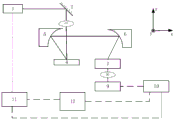
(1)实现所述方法的测量系统由光载流子辐射测量系统和光致发光光谱测量系统综合组成,两系统共用激光光源1,平面高反镜或全反镜2,聚焦透镜3,样品台4,离轴抛物面反射镜5和6,组合透镜系统8,光电探测器9,锁相放大器10,函数发生器11,上位机或计算机12,以上部件构成光载流子辐射测量系统,当系统工作于光致发光光谱系统时,在组合透镜系统8之前加入单色仪7。上位机12通过对函数发生器11进行控制来实现对激励光的调制;光源1发出的激光经过聚焦透镜3后聚焦在样品池4中的样品表面,样品吸收激励光能量后经过辐射复合发出的光致发光信号通过离轴抛物面镜5和6收集后,再经组合透镜系统8聚焦到光电探测器9后转化为电信号,电信号传输至锁相放大器10滤除噪声进行放大,放大后的信号传入数据处理计算机12进行记录;而后计算机12对函数发生器11进行调控并重复上述信号采集过程对样品进行扫频。通过改变测量实验条件,分别得到不同条件下光致发光信号相位与激励频率的关系,经分析计算得出载流子寿命,从以下三个方面改变实验条件:a)当系统工作在光载流子辐射测量系统状态时,此时光电探测器9接收的信号包含待测半导体材料整个发光光谱范围内全部光信号对波长进行积分的信号;通过改变激励光 1频率可以得到光致发光波长积分的总信号与频率之间的关系,由信号幅值及相位与频率的关系可计算得到载流子多重寿命的有效寿命。b)当系统工作在光致发光光谱测量系统状态时,光致发光信号经单色仪7再聚焦到光电探测器9上,通过单色仪7扫描波长可得到待测半导体样品的发光光谱,通过改变激励光1的频率,可以得到不同频率下的光致发光光谱,从而可由数据分析得到不同波长下的光致发光信号幅值及相位与频率的关系,由信号幅值及相位与频率的关系可计算得到产生对应波长光致发光信号的载流子寿命。c)根据b) 中得到的发光光谱,可确定材料的多个发光峰中心波长,将单色仪7通光波长分别固定在各发光峰中心,改变激励光1频率,进行频率扫描,分别得到各发光峰中心波长处光致发光信号幅值及相位与频率的关系,从而可计算得到产生对应波长光致发光信号的载流子寿命;a) 中得到的有效寿命是b)或c)中得到的多个寿命的加权值;b)和c)中在同一波长下得到的寿命值相等,两种条件可作为相互验证的方法。(1) The measurement system for realizing the method is composed of a photocarrier radiation measurement system and a photoluminescence spectrum measurement system. The two systems share a laser light source 1, a flat high-reflection mirror or a
由a)、b)、c)测试过程分别得到的信号幅值及相位与频率的关系曲线,使用非线性多参数拟合方法,将信号幅值及相位按公式(1)进行拟合。The relationship curve of signal amplitude and phase and frequency obtained by a), b), and c) test process respectively, using nonlinear multi-parameter fitting method, the signal amplitude and phase are fitted according to formula (1).


其中,由a)过程所得信号是所有光致发光信号的叠加,对测试数据拟合得到的载流子寿命由多个发光驰豫过程所对应的载流子寿命加权构成,因此可由a)过程得到载流子的多重寿命分布谱线;由b)过程可得各个发光波长下信号与频率的关系,对测试数据拟合得到的载流子寿命是各波长下发光驰豫过程所对应的载流子寿命;由c)过程可得各个发光峰中心波长下信号与频率的关系,对测试数据拟合得到的载流子寿命是各中心发光驰豫过程所对应的载流子寿命;对同一块样品将b)过程中发光峰对应波长数据提取出来应与c)过程数据一致。Among them, the signal obtained by the a) process is the superposition of all photoluminescence signals, and the carrier lifetime obtained by fitting the test data is composed of the carrier lifetime weights corresponding to multiple luminescence relaxation processes, so the a) process can be used. Obtain the multiple lifetime distribution spectral lines of the carriers; the relationship between the signal and the frequency at each luminescence wavelength can be obtained from the process b), and the carrier lifetime obtained by fitting the test data is the carrier corresponding to the luminescence relaxation process at each wavelength. The carrier lifetime; the relationship between the signal and the frequency at the center wavelength of each luminescence peak can be obtained from the process c), and the carrier lifetime obtained by fitting the test data is the carrier lifetime corresponding to the luminescence relaxation process of each center; for the same The wavelength data corresponding to the luminescence peak in the process b) extracted from a sample should be consistent with the data in the process c).
由b)过程所得各个载流子寿命应与a)得到载流子寿命分布中的各寿命分量相对应,由 c)过程所得各中心波长发光峰对应的载流子寿命应与a)得到载流子寿命分布中的主要寿命分量相对应。The lifetime of each carrier obtained from the process b) should correspond to each lifetime component of the carrier lifetime distribution obtained from a), and the lifetime of each carrier corresponding to the luminescence peak of each central wavelength obtained from the process of c) should be the same as that obtained from a) . The main lifetime components in the carrier lifetime distribution correspond to .
(2)对于不同厚度的半导体待测样品可以通过调节样品台4的高度保证样品处于激光和离焦抛物面镜5的焦点。(2) For semiconductor samples of different thicknesses, the height of the
(3)所述的离轴抛物面镜5用于收集从样品表面发射的光致发光信号,因光致发光信号在样品表面上方全空间呈球面分布,因此离焦抛物面镜5的焦距应尽可能短以提高信号的收集率。(3) The off-axis
附图说明Description of drawings
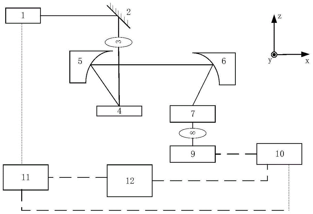
图1为本发明所述技术方案的实施示意图。FIG. 1 is a schematic diagram of the implementation of the technical solution of the present invention.
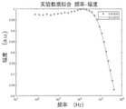
图2是由光电探测器9采集得到的振幅信号A1在去除系统频响A0后。使用公式拟合的拟合曲线及振幅信号FIG. 2 shows the amplitude signal A 1 collected by the photodetector 9 after removing the system frequency response A 0 . Fitted curve and amplitude signal fitted using formula
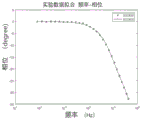
图3是由光电探测器9采集得到的相位信号P1在去除系统频响P0后。使用公式拟合的拟合曲线及相位信号FIG. 3 shows the phase signal P 1 collected by the photodetector 9 after removing the system frequency response P 0 . Fitted curve and phase signal using formula fit
图1中:1为激光光源,2为平面高反镜或全反镜,3为聚焦透镜,4为温控系统样品池, 5和6为离轴抛物面镜,7为单色仪,8为组合透镜系统,9为光电探测器,10为锁相放大器,11为函数发生器,12为上位机或计算机1。图中的实线为光路,虚线为信号线。In Figure 1: 1 is a laser light source, 2 is a flat high-reflection mirror or a total reflection mirror, 3 is a focusing lens, 4 is a temperature control system sample cell, 5 and 6 are off-axis parabolic mirrors, 7 is a monochromator, and 8 is a In the combined lens system, 9 is a photodetector, 10 is a lock-in amplifier, 11 is a function generator, and 12 is a host computer or computer 1. The solid line in the figure is the optical path, and the dotted line is the signal line.
具体实施方式Detailed ways
下面结合图1具体描述本发明提出的一种用于测量多发光峰半导体材料中载流子多重寿命的方法,然而应当理解,附图的提供仅为了更好地理解本发明,它们不应该理解成对本发明的限制。具体的实施步骤如下:A method for measuring the multiple lifetimes of carriers in a semiconductor material with multiple luminescence peaks proposed by the present invention will be described in detail below in conjunction with FIG. to limit the invention. The specific implementation steps are as follows:
(1)搭建光载流子副射测量系统。将图1所示的xyz坐标系定义为实验坐标系,即实验中以此为参考坐标系,其中x、z方向在纸面内,y方向为垂直纸面射出方向。(1) Build a photocarrier secondary emission measurement system. The xyz coordinate system shown in Figure 1 is defined as the experimental coordinate system, that is, it is used as the reference coordinate system in the experiment, in which the x and z directions are in the paper surface, and the y direction is the ejection direction perpendicular to the paper surface.
a.调整光源1和反射镜2以及聚焦透镜3,使得光源出射光束沿实验坐标系z方向射出,且焦点位于样品台4的样品上。a. Adjust the light source 1 , the
b.调整光路使离轴抛物面镜5的焦点与光源在样品台4上的焦点重合,使离焦抛物面镜6在5反射的平行光路上。b. Adjust the optical path so that the focus of the off-axis
c.将单色仪7进光口对准离焦抛物面镜6的焦点,并且根据扫描光谱的分辨率调整单色仪狭缝宽度。c. Align the light inlet of the monochromator 7 with the focus of the defocused parabolic mirror 6, and adjust the width of the monochromator slit according to the resolution of the scanned spectrum.
d.调整组合透镜系统8使单色仪7出射光的焦点在光电探测器9的光敏面上。d. Adjust the combined lens system 8 so that the focus of the light emitted from the monochromator 7 is on the photosensitive surface of the photodetector 9 .
e.连接光电探测器9到信号采集和处理计算机12上,调整光电探测器9和组合透镜8 以及微调反射镜2和单色仪7的位置以及样品池4的高度,使得光电探测器9信号最大,此时,光电探测器9的光敏面位于组合透镜8的焦点处并收集所有的入射光。e. Connect the photodetector 9 to the signal acquisition and
f.将样品台4清空,通过计算机12设定频率/光谱/温度扫描范围,得到系统的在设定频谱的频率响应幅度信号A0和相位信号P0。f. Empty the
(2)待测半导体样品信号测量。将待测样品放入样品台4,调整样品台4高度,使得光电探测器9的信号值最大。(2) Signal measurement of the semiconductor sample to be tested. Put the sample to be tested into the
a.计算机对函数发生器进行调控并开展权利要求书中的a)、b)、c)测试过程,计算机12 通过光电探测器9测得信号A1或P1按公式A2=A1/A0及相位P1按公式P2=P1-P0得到去除系统频响后的信号;将去除频响后的幅度信号A2和去除频响后的相位信号P2分别按公式(1)进行拟合,可得到待测半导体样品的载流子寿命τi和对应寿命载流子光致发光占比Ki。a. The computer controls the function generator and carries out the testing process of a), b), and c) in the claims. The
下面给出本发明检测装置的具体实施例,具体实施例仅用于详细说明本发明,并不限制本申请权利要求的保护范围。Specific embodiments of the detection device of the present invention are given below, and the specific embodiments are only used to describe the present invention in detail, and do not limit the protection scope of the claims of the present application.
实例1Example 1
本发明实例1中的待测样品是粒径3-5nm、发光峰为950-1350nm的量子点溶液样品经 1000r/m 10s和2500r/m 25s的旋涂工艺涂附在玻璃片上的薄膜样品。The sample to be tested in Example 1 of the present invention is a film sample of a quantum dot solution sample with a particle size of 3-5nm and a luminescence peak of 950-1350nm, which is coated on a glass plate by spin coating processes of 1000r/m 10s and 2500r/m 25s.
图2是由光电探测器9采集得到的振幅信号A1在去除系统频响A0后。使用公式
图3是由光电探测器9采集得到的相位信号P1在去除系统频响P0后。使用公式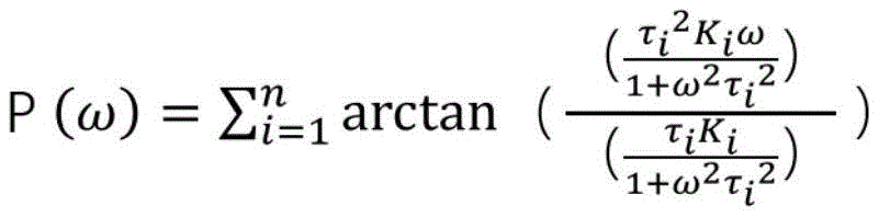
Claims (7)
Priority Applications (1)
| Application Number | Priority Date | Filing Date | Title |
|---|---|---|---|
| CN201911352634.2A CN111257713A (en) | 2019-12-25 | 2019-12-25 | A method for measuring multiple lifetimes of carriers in semiconductor materials with multiple luminescence peaks |
Applications Claiming Priority (1)
| Application Number | Priority Date | Filing Date | Title |
|---|---|---|---|
| CN201911352634.2A CN111257713A (en) | 2019-12-25 | 2019-12-25 | A method for measuring multiple lifetimes of carriers in semiconductor materials with multiple luminescence peaks |
Publications (1)
| Publication Number | Publication Date |
|---|---|
| CN111257713A true CN111257713A (en) | 2020-06-09 |
Family
ID=70948522
Family Applications (1)
| Application Number | Title | Priority Date | Filing Date |
|---|---|---|---|
| CN201911352634.2A Pending CN111257713A (en) | 2019-12-25 | 2019-12-25 | A method for measuring multiple lifetimes of carriers in semiconductor materials with multiple luminescence peaks |
Country Status (1)
| Country | Link |
|---|---|
| CN (1) | CN111257713A (en) |
Cited By (2)
| Publication number | Priority date | Publication date | Assignee | Title |
|---|---|---|---|---|
| CN110646384A (en) * | 2019-09-24 | 2020-01-03 | 西安工业大学 | A kind of optical measurement method of semiconductor material resistivity |
| CN121431449A (en) * | 2025-10-20 | 2026-01-30 | 中国电子技术标准化研究院((工业和信息化部电子工业标准化研究院)(工业和信息化部电子第四研究院)) | A method for calibration and extraction of transient photoconductive signals applicable to ultrathin films |
Citations (5)
| Publication number | Priority date | Publication date | Assignee | Title |
|---|---|---|---|---|
| CN101527273A (en) * | 2009-04-10 | 2009-09-09 | 中国科学院光电技术研究所 | Device and method for measuring properties of semiconductor materials |
| CN203011574U (en) * | 2013-01-17 | 2013-06-19 | 杭州电子科技大学 | A burning temperature sensing device based on terahertz pulse measurement |
| CN103929128A (en) * | 2014-04-22 | 2014-07-16 | 哈尔滨工业大学 | Method and system for detecting transmission characteristics of minority carriers of silicon slice and silicon-based solar cell |
| US9160137B1 (en) * | 2014-05-09 | 2015-10-13 | Max-Planck-Gesellschaft zur Förderung der Wissenschaften e. V. | Method and device for creating supercontinuum light pulses |
| JP2019039705A (en) * | 2017-08-23 | 2019-03-14 | 浜松ホトニクス株式会社 | Tunnel current control device and tunnel current control method |
-
2019
- 2019-12-25 CN CN201911352634.2A patent/CN111257713A/en active Pending
Patent Citations (5)
| Publication number | Priority date | Publication date | Assignee | Title |
|---|---|---|---|---|
| CN101527273A (en) * | 2009-04-10 | 2009-09-09 | 中国科学院光电技术研究所 | Device and method for measuring properties of semiconductor materials |
| CN203011574U (en) * | 2013-01-17 | 2013-06-19 | 杭州电子科技大学 | A burning temperature sensing device based on terahertz pulse measurement |
| CN103929128A (en) * | 2014-04-22 | 2014-07-16 | 哈尔滨工业大学 | Method and system for detecting transmission characteristics of minority carriers of silicon slice and silicon-based solar cell |
| US9160137B1 (en) * | 2014-05-09 | 2015-10-13 | Max-Planck-Gesellschaft zur Förderung der Wissenschaften e. V. | Method and device for creating supercontinuum light pulses |
| JP2019039705A (en) * | 2017-08-23 | 2019-03-14 | 浜松ホトニクス株式会社 | Tunnel current control device and tunnel current control method |
Non-Patent Citations (2)
| Title |
|---|
| ROBERT MAIWALD等: "Ions inside a parabolic mirror - Surrounding absorbers with reflective geometry allows for efficient free space-coupling", 《2011 CONFERENCE ON LASERS AND ELECTRO-OPTICS EUROPE AND 12TH EUROPEAN QUANTUM ELECTRONICS CONFERENCE》 * |
| 彭龙瑶等: "基于硅基石墨烯的全光控太赫兹波强度调制系统研究", 《红外与激光工程》 * |
Cited By (3)
| Publication number | Priority date | Publication date | Assignee | Title |
|---|---|---|---|---|
| CN110646384A (en) * | 2019-09-24 | 2020-01-03 | 西安工业大学 | A kind of optical measurement method of semiconductor material resistivity |
| CN110646384B (en) * | 2019-09-24 | 2021-12-14 | 西安工业大学 | A kind of optical measurement method of semiconductor material resistivity |
| CN121431449A (en) * | 2025-10-20 | 2026-01-30 | 中国电子技术标准化研究院((工业和信息化部电子工业标准化研究院)(工业和信息化部电子第四研究院)) | A method for calibration and extraction of transient photoconductive signals applicable to ultrathin films |
Similar Documents
| Publication | Publication Date | Title |
|---|---|---|
| US9164042B2 (en) | Device for detecting foreign matter and method for detecting foreign matter | |
| CN101527273B (en) | Measuring device for semiconductor material characteristics | |
| CN110646384B (en) | A kind of optical measurement method of semiconductor material resistivity | |
| CN103929128B (en) | The minority carrier transmission characteristic detection method of a kind of silicon chip and silica-based solar cell | |
| CN101551324B (en) | Device and method for measuring characteristics of semiconductor materials based on dual probe beams | |
| CN108267420A (en) | Seed aqueous amount detection systems and method | |
| CN105866061B (en) | The anticoincidence pulse detection device and anticoincidence pulse detection method of THz wave time-domain information | |
| CN104483104A (en) | Spectral response analysis system for photoelectric detector | |
| CN117012663B (en) | Wafer defect detection system and method | |
| CN103543130B (en) | Method for eliminating system frequency response influence of semiconductor material characteristic measuring device in photocarrier radiation technology | |
| CN111257713A (en) | A method for measuring multiple lifetimes of carriers in semiconductor materials with multiple luminescence peaks | |
| CN103901335A (en) | Infrared polarization optical imaging detecting method and system for service life distribution of minority carriers of semi-conductor | |
| CN117650755A (en) | A carrier dynamics testing method and system applied to optoelectronic devices | |
| CN115728250B (en) | Semiconductor carrier dynamics test instrument and test method | |
| CN113109282B (en) | A photothermal deflection spectrum testing device with wide wavelength coverage | |
| CN114235764A (en) | Quantitative imaging characterization method for surface recombination rate of semiconductor wafer current carrier | |
| CN115015156B (en) | Wafer detection device and detection method | |
| CN118732310A (en) | A method for modulating spectrum of semiconductor materials and optical path system | |
| CN109239023B (en) | Semiconductor material characteristic measuring method based on free carrier absorption imaging | |
| CN116183545A (en) | Terahertz spectrum detection device with low cost and high signal-to-noise ratio | |
| CN109142287A (en) | A kind of semiconductor material characteristic measurement method based on photocarrier radiation | |
| JP3674738B2 (en) | Minority carrier lifetime measurement device | |
| CN223122857U (en) | Spectral measurement device for sub-bandgap photoelectric signal characterization | |
| EP4456418A1 (en) | Method and device for characterization of photovoltaic solar elements | |
| JP3648019B2 (en) | Minority carrier lifetime measurement device |
Legal Events
| Date | Code | Title | Description |
|---|---|---|---|
| PB01 | Publication | ||
| PB01 | Publication | ||
| SE01 | Entry into force of request for substantive examination | ||
| SE01 | Entry into force of request for substantive examination | ||
| WD01 | Invention patent application deemed withdrawn after publication |
Application publication date: 20200609 |
|
| WD01 | Invention patent application deemed withdrawn after publication |