CN102160459A - Light-emitting device, production method therefor, and display containing same - Google Patents
Light-emitting device, production method therefor, and display containing same Download PDFInfo
- Publication number
- CN102160459A CN102160459A CN2009801372051A CN200980137205A CN102160459A CN 102160459 A CN102160459 A CN 102160459A CN 2009801372051 A CN2009801372051 A CN 2009801372051A CN 200980137205 A CN200980137205 A CN 200980137205A CN 102160459 A CN102160459 A CN 102160459A
- Authority
- CN
- China
- Prior art keywords
- layer
- light
- light emitting
- emitting device
- convex pattern
- Prior art date
- Legal status (The legal status is an assumption and is not a legal conclusion. Google has not performed a legal analysis and makes no representation as to the accuracy of the status listed.)
- Granted
Links
Images


Classifications
-
- H—ELECTRICITY
- H05—ELECTRIC TECHNIQUES NOT OTHERWISE PROVIDED FOR
- H05B—ELECTRIC HEATING; ELECTRIC LIGHT SOURCES NOT OTHERWISE PROVIDED FOR; CIRCUIT ARRANGEMENTS FOR ELECTRIC LIGHT SOURCES, IN GENERAL
- H05B33/00—Electroluminescent light sources
- H05B33/10—Apparatus or processes specially adapted to the manufacture of electroluminescent light sources
-
- H—ELECTRICITY
- H05—ELECTRIC TECHNIQUES NOT OTHERWISE PROVIDED FOR
- H05B—ELECTRIC HEATING; ELECTRIC LIGHT SOURCES NOT OTHERWISE PROVIDED FOR; CIRCUIT ARRANGEMENTS FOR ELECTRIC LIGHT SOURCES, IN GENERAL
- H05B33/00—Electroluminescent light sources
- H05B33/12—Light sources with substantially two-dimensional [2D] radiating surfaces
- H05B33/14—Light sources with substantially two-dimensional [2D] radiating surfaces characterised by the chemical or physical composition or the arrangement of the electroluminescent material, or by the simultaneous addition of the electroluminescent material in or onto the light source
-
- H—ELECTRICITY
- H05—ELECTRIC TECHNIQUES NOT OTHERWISE PROVIDED FOR
- H05B—ELECTRIC HEATING; ELECTRIC LIGHT SOURCES NOT OTHERWISE PROVIDED FOR; CIRCUIT ARRANGEMENTS FOR ELECTRIC LIGHT SOURCES, IN GENERAL
- H05B33/00—Electroluminescent light sources
- H05B33/12—Light sources with substantially two-dimensional [2D] radiating surfaces
- H05B33/22—Light sources with substantially two-dimensional [2D] radiating surfaces characterised by the chemical or physical composition or the arrangement of auxiliary dielectric or reflective layers
-
- H—ELECTRICITY
- H10—SEMICONDUCTOR DEVICES; ELECTRIC SOLID-STATE DEVICES NOT OTHERWISE PROVIDED FOR
- H10K—ORGANIC ELECTRIC SOLID-STATE DEVICES
- H10K50/00—Organic light-emitting devices
- H10K50/80—Constructional details
- H10K50/85—Arrangements for extracting light from the devices
-
- H—ELECTRICITY
- H10—SEMICONDUCTOR DEVICES; ELECTRIC SOLID-STATE DEVICES NOT OTHERWISE PROVIDED FOR
- H10K—ORGANIC ELECTRIC SOLID-STATE DEVICES
- H10K50/00—Organic light-emitting devices
- H10K50/80—Constructional details
- H10K50/85—Arrangements for extracting light from the devices
- H10K50/854—Arrangements for extracting light from the devices comprising scattering means
-
- H—ELECTRICITY
- H10—SEMICONDUCTOR DEVICES; ELECTRIC SOLID-STATE DEVICES NOT OTHERWISE PROVIDED FOR
- H10K—ORGANIC ELECTRIC SOLID-STATE DEVICES
- H10K50/00—Organic light-emitting devices
- H10K50/80—Constructional details
- H10K50/85—Arrangements for extracting light from the devices
- H10K50/856—Arrangements for extracting light from the devices comprising reflective means
-
- H—ELECTRICITY
- H10—SEMICONDUCTOR DEVICES; ELECTRIC SOLID-STATE DEVICES NOT OTHERWISE PROVIDED FOR
- H10K—ORGANIC ELECTRIC SOLID-STATE DEVICES
- H10K59/00—Integrated devices, or assemblies of multiple devices, comprising at least one organic light-emitting element covered by group H10K50/00
- H10K59/80—Constructional details
- H10K59/875—Arrangements for extracting light from the devices
- H10K59/878—Arrangements for extracting light from the devices comprising reflective means
Landscapes
- Physics & Mathematics (AREA)
- Optics & Photonics (AREA)
- Engineering & Computer Science (AREA)
- Manufacturing & Machinery (AREA)
- Electroluminescent Light Sources (AREA)
- Devices For Indicating Variable Information By Combining Individual Elements (AREA)
Abstract
本发明提供一种发光装置,其按顺序包括含有发光部分的发光层、中间层、和精细凹凸图案,其中中间层设置于发光层的第二表面上,所述表面和发光层的第一表面相对,其中精细凹凸图案的横截面形状具有相对于发光层凸出和凹进的部分,并反射从发光层发射的光,且其中中间层的至少一部分的折射率为0.9n到1.1n,其中n表示所述发光部分相对于具有主发光波长的光的折射率。

The present invention provides a light-emitting device, which sequentially includes a light-emitting layer containing a light-emitting part, an intermediate layer, and a fine concave-convex pattern, wherein the intermediate layer is provided on the second surface of the light-emitting layer, the surface and the first surface of the light-emitting layer In contrast, wherein the cross-sectional shape of the fine concavo-convex pattern has convex and concave portions relative to the light-emitting layer, and reflects light emitted from the light-emitting layer, and wherein at least a part of the intermediate layer has a refractive index of 0.9n to 1.1n, wherein n represents the refractive index of the light emitting portion with respect to light having a dominant light emission wavelength.
Description
技术领域technical field
本发明涉及发光装置、其生产方法和含有所述发光装置的显示器,更具体地,涉及诸如有机电致发光装置(有机EL装置)、无机电致发光装置(无机EL装置)和发光二极管(LED),它们的生产方法,和含有所述发光装置的显示器。The present invention relates to a light-emitting device, a production method thereof, and a display including the light-emitting device, and more particularly, to devices such as organic electroluminescent devices (organic EL devices), inorganic electroluminescent devices (inorganic EL devices), and light-emitting diodes (LEDs). ), their production methods, and displays containing said light emitting devices.
背景技术Background technique
例如,在如图3所示的有机EL装置105中,从放在反射层101上的EL发光层102发射的光束在EL发光层102和密封层103之间的空间或在密封层103和外界104之间的空间反射,导致光提取效率降低。For example, in the organic EL device 105 as shown in FIG. The spatial reflection between 104 leads to a decrease in light extraction efficiency.
此处,关于发生光折射的界面上的光反射率,当界面是平的时,反射率取决于光的入射角和共享界面的介质之间的折射率差异。例如,当它们之间的折射率差异大时,界面上的反射率变高。此外,当光以大于临界角的入射角从具有高折射率的介质行进至具有低折射率的介质时,100%的光被反射。Here, regarding the reflectance of light on an interface where light refraction occurs, when the interface is flat, the reflectance depends on the incident angle of light and the difference in refractive index between media sharing the interface. For example, when the difference in refractive index between them is large, the reflectance on the interface becomes high. Furthermore, when light travels from a medium with a high refractive index to a medium with a low refractive index at an incident angle greater than the critical angle, 100% of the light is reflected.
临界角θc是当光从具有高折射率的物质行进至具有低折射率的物质时光被全反射的最小入射角,且以下列等式:θc=arcsin(n2/n1)表示,其中n1表示光行经的物质的折射率;n2表示光进入的物质的折射率;且n2<n1。The critical angle θ c is the minimum incident angle at which light is totally reflected when it travels from a substance with a high refractive index to a substance with a low refractive index, and is represented by the following equation: θ c =arcsin(n 2 /n 1 ), Where n 1 represents the refractive index of the material through which the light travels; n 2 represents the refractive index of the material into which the light enters; and n 2 <n 1 .
图4是用于描述上述现象的说明性视图。在该图中,附图标记111和112分别表示具有折射率n1的第一层和具有折射率n2的第二层。此处,当光以相对于法线(标准线)的临界角θc的入射角行进至第一层和第二层之间的界面110时,光在界面110上全反射,因此不能从第二层112提取。另外,以相对于标准线的大于临界角θc的入射角θx行进的光也在界面110上全反射,因此不能从第二层112提取。FIG. 4 is an explanatory view for describing the above phenomenon. In the figure,
另外,以相对于标准线的小于临界角θc的入射角θy行进的光透过界面110从第二层112射到第一层111。In addition, light traveling at an incident angle θy smaller than the critical angle θc with respect to the standard line passes through the
当光从高折射率介质射到低折射率介质时,光全反射的发光装置存在光提取效率低的问题。When light irradiates from a high-refractive-index medium to a low-refractive-index medium, the light-emitting device with total light reflection has the problem of low light extraction efficiency.
有鉴于此,已提出具有多种结构的发光装置,由此尝试改进光提取效率。In view of this, light emitting devices having various structures have been proposed, thereby attempting to improve light extraction efficiency.
已提出的一种发光装置是有机电致发光装置,包括阳极、阴极、一个或多个含有设置于电极之间的发光层的有机层和衍射光栅或波带片,其中衍射光栅或波带片设置于防止装置中界面上的全反射的位置(参见专利文献1)。A light-emitting device that has been proposed is an organic electroluminescent device comprising an anode, a cathode, one or more organic layers including a light-emitting layer disposed between the electrodes, and a diffraction grating or zone plate, wherein the diffraction grating or zone plate Provided at a position to prevent total reflection on the interface in the device (see Patent Document 1).
然而,在专利文献1公开的发光装置中,发射的光穿过低折射率层到达衍射光栅或波带片,因此对防止全反射产生限制。However, in the light-emitting device disclosed in
此外,另一种已提出的发光装置在和发光表面相对的背表面上含有凹凸图案的散射层,其中散射层为了光提取而反射/散射从发光层穿过中间层射向发光表面的光(参见非专利文献1和2)。In addition, another proposed light-emitting device has a scattering layer having a concavo-convex pattern on the back surface opposite to the light-emitting surface, wherein the scattering layer reflects/scatters light emitted from the light-emitting layer to the light-emitting surface through an intermediate layer for light extraction ( See
如图5所示,一种常规已知的发光装置按此顺序包括含有发光部分204的发光层202、中间层205、和精细凹凸图案206,其中中间层和精细凹凸图案位于发光层202的第二表面203B上,所述表面和发光层的第一表面203A相对。As shown in FIG. 5, a conventionally known light-emitting device includes, in this order, a light-emitting
然而,这样的常规发光装置具有折射率不同的发光层和中间层(例如,发光层的折射率n:1.8,且中间层的折射率n:1.5),因此产生从发光层202的光提取效率因全反射而低的问题。However, such a conventional light-emitting device has a light-emitting layer and an intermediate layer having different refractive indices (for example, the refractive index n of the light-emitting layer: 1.8, and the refractive index n of the intermediate layer: 1.5), thus resulting in a light extraction efficiency from the light-emitting
具体地,从发光部分204射到发光层202的第二表面203B且入射角为大于临界角θc的θx的光束210a在第二表面203B全反射,且不能从发光部分204提取。Specifically, the
此外,在发光部分204和密封层207之间的界面上朝向第二表面203B全反射且入射角是大于临界角θc的θx的光束210b在第二表面203B全反射,且不能从发光部分204提取。In addition, the
此外,在发光层202的第一表面203A上朝向第二表面203B全反射且入射角是大于临界角θc的θx的光束210c在第二表面203B全反射,且不能从发光部分204提取。In addition, the
考虑到上面所述,对于改进了光提取效率(light-extraction efficiency)的发光装置存在需求。In view of the above, there is a need for a light emitting device with improved light-extraction efficiency.
引用列表reference list
专利文献patent documents
PTL 1:日本专利No.2991183PTL 1: Japanese Patent No.2991183
非专利文献non-patent literature
NPL 1:Norihiko Kamiura及其他四人,“Studies on OLED Light Extraction Enhancement”,由THE INSTITUTE OF ELECTRONICS,INFORMATION AND COMMUNICATION ENGINEERS编辑,TECHNICAL REPORT OF IEICE,EID2007-102,OME2007-84(2008-03),1到4页NPL 1: Norihiko Kamiura and four others, "Studies on OLED Light Extraction Enhancement", edited by THE INSTITUTE OF ELECTRONICS, INFORMATION AND COMMUNICATION ENGINEERS, TECHNICAL REPORT OF IEICE, EID2007-102, OME2007-84(2008-03) to
NPL 2:Hiroshi Sano及其他12人,“An Organic Light-Emitting Diode with Highly Efficient Light Extraction Using Newly Developed Diffraction Layer”,SID 08DIGEST,515到517页NPL 2: Hiroshi Sano and 12 others, "An Organic Light-Emitting Diode with Highly Efficient Light Extraction Using Newly Developed Diffraction Layer", SID 08DIGEST, pp. 515-517
发明内容Contents of the invention
本发明的目的在于提供改进了光提取效率的发光装置;和所述发光装置的生产方法;以及含有所述发光装置的显示器。这些可以解决上面存在的问题。An object of the present invention is to provide a light emitting device with improved light extraction efficiency; and a production method of the light emitting device; and a display including the light emitting device. These can solve the problems existing above.
用于解决上述问题的方法如下。A method for solving the above-mentioned problems is as follows.
<1>发光装置,其按顺序包括:<1> A light emitting device comprising in order:
含有发光部分的发光层,a luminescent layer comprising a luminescent moiety,
中间层,和middle layer, and
精细凹凸图案,fine embossed pattern,
其中中间层设置于发光层的第二表面上,所述第二表面和发光层的第一表面相对,Wherein the intermediate layer is disposed on the second surface of the light-emitting layer, the second surface is opposite to the first surface of the light-emitting layer,
其中精细凹凸图案具有相对于发光层凸出和凹进的部分的横截面形状并反射从发光层发射的光,且wherein the fine concavo-convex pattern has a cross-sectional shape of a portion convex and concave with respect to the light emitting layer and reflects light emitted from the light emitting layer, and
其中中间层的至少一部分的折射率为0.9n到1.1n,其中n表示所述发光部分相对于具有主发光波长的光的折射率。Wherein at least a portion of the intermediate layer has a refractive index of 0.9n to 1.1n, where n represents the refractive index of the light emitting portion with respect to light having a dominant light emission wavelength.
<2>根据上面<1>的发光装置,其中精细凹凸图案的间距(pitch interval)为0.01λ到100λ,其中λ表示从发光层发射的光的主发光波长。<2> The light-emitting device according to the above <1>, wherein a pitch interval of the fine concavo-convex pattern is 0.01λ to 100λ, where λ represents a dominant emission wavelength of light emitted from the light-emitting layer.
<3>根据上面<1>和<2>中任意一项的发光装置,其中发光层含有两个或更多个发光部分。<3> The light-emitting device according to any one of <1> and <2> above, wherein the light-emitting layer contains two or more light-emitting portions.
<4>根据上面<1>到<3>中任意一项的发光装置,其中精细凹凸图案由加热模式光刻胶(resist)制成。<4> The light-emitting device according to any one of <1> to <3> above, wherein the fine concavo-convex pattern is made of a heating pattern resist.
<5>根据上面<1>到<4>中任意一项的发光装置,其中精细凹凸图案包括反射层。<5> The light-emitting device according to any one of <1> to <4> above, wherein the fine concavo-convex pattern includes a reflective layer.
<6>根据上面<5>的发光装置,其中反射层的厚度为10nm到10,000nm。<6> The light-emitting device according to the above <5>, wherein the reflective layer has a thickness of 10 nm to 10,000 nm.
<7>根据上面<1>到<6>中任意一项的发光装置,其中中间层的折射率为1.55到3.0。<7> The light-emitting device according to any one of <1> to <6> above, wherein the intermediate layer has a refractive index of 1.55 to 3.0.
<8>根据上面<1>到<7>中任意一项的发光装置,其中精细凹凸图案的间距为50nm到10μm。<8> The light-emitting device according to any one of <1> to <7> above, wherein the pitch of the fine concave-convex pattern is 50 nm to 10 μm.
<9>根据上面<1>到<8>中任意一项的发光装置,其中发光层还包括用于密封发光部分的密封层,且其中密封层的材料是丙烯酸树脂、环氧树脂、含氟树脂、有机硅树脂、橡胶树脂和酯树脂的中任意种类。<9> The light-emitting device according to any one of <1> to <8> above, wherein the light-emitting layer further includes a sealing layer for sealing the light-emitting part, and wherein the material of the sealing layer is acrylic resin, epoxy resin, fluorine-containing Any kind of resin, silicone resin, rubber resin and ester resin.
<10>根据上面<1>到<5>中任意一项的发光装置的生产方法,包括:<10> The method for producing a light-emitting device according to any one of <1> to <5> above, comprising:
形成含有发光部分的发光层,forming a light-emitting layer containing a light-emitting moiety,
在发光层的第二表面上形成中间层,所述表面和发光层的第一表面相对,和forming an intermediate layer on a second surface of the luminescent layer opposite to the first surface of the luminescent layer, and
在中间层上形成精细凹凸图案,其横截面形状具有相对于发光层的凸出和凹进,所述精细凹凸图案反射从发光层发射的光,forming a fine concavo-convex pattern, the cross-sectional shape of which has protrusions and concavities with respect to the light-emitting layer, on the intermediate layer, the fine concavo-convex pattern reflecting light emitted from the light-emitting layer,
其中精细凹凸图案通过加热模式光刻形成。The fine concave-convex pattern is formed by heating mode photolithography.
<11>显示器,包括:根据上面<1>到<5>的发光装置。<11> A display comprising: the light emitting device according to <1> to <5> above.
本发明可以提供改进了光提取效率的发光装置;和所述发光装置的生产方法;以及含有所述发光装置的显示器,它们可以解决上面存在的问题。The present invention can provide a light emitting device with improved light extraction efficiency; and a production method of the light emitting device; and a display including the light emitting device, which can solve the above existing problems.
附图说明Description of drawings
图1是作为本发明发光装置的有机EL装置的剖视图。Fig. 1 is a cross-sectional view of an organic EL device as a light-emitting device of the present invention.
图2是根据本发明另一实施方案的发光装置,和含有所述发光装置的显示器的说明性剖视图。2 is an explanatory cross-sectional view of a light emitting device according to another embodiment of the present invention, and a display including the light emitting device.
图3是常规发光装置的说明性剖视图。Fig. 3 is an explanatory cross-sectional view of a conventional light emitting device.
图4是用于描述第一层和第二层之间的界面上的临界角θc的示意图。FIG. 4 is a schematic diagram for describing the critical angle θ c at the interface between the first layer and the second layer.
图5是用于描述常规发光装置具有的问题的示意图。FIG. 5 is a schematic diagram for describing problems that a conventional light emitting device has.
具体实施方式Detailed ways
下面将详细描述本发明的发光装置,所述发光装置的生产方法,和含有所述发光装置的显示器。The light emitting device of the present invention, a method for producing the light emitting device, and a display including the light emitting device will be described in detail below.
(发光装置)(light emitting device)
本发明的发光装置按此顺序包括含有发光部分的发光层、中间层、和精细凹凸图案。精细凹凸图案反射从发光层发射的光且其横截面形状具有相对于发光层凸出和凹进的部分。The light-emitting device of the present invention includes, in this order, a light-emitting layer including a light-emitting portion, an intermediate layer, and a fine concavo-convex pattern. The fine concavo-convex pattern reflects light emitted from the light emitting layer and has a cross-sectional shape having convex and concave portions relative to the light emitting layer.
图1是这样的发光装置的结构示意图。在该图中,中间层5和精细凹凸图案6按此顺序设置于发光层2的第二表面3B上,所述表面和第一表面3A相对。(发光表面)FIG. 1 is a schematic structural view of such a light emitting device. In this figure, the
<发光层><luminescent layer>
发光层2包括发光部分4。The
用于发光部分4的装置没有特别限制且可根据目的适当选择。发光部分可以是例如有机EL装置、无机EL装置、LED和光电二极管。The device used for the
<<密封层>><<sealing layer>>
在发光层2中,发光部分4用密封层7密封。In the
密封层7防止发光部分4由于暴露于空气因氧气和水分而性能降低。The
此外,发光层2可含有水分吸收剂或惰性液体。水分吸收剂没有特别限制,且其具体实例包括氧化钡、氧化钠、氧化钾、氧化钙、硫酸钠、硫酸钙、硫酸镁、五氧化磷、氯化钙、氯化镁、氯化铜、氟化铯、氟化铌、溴化钙、溴化钒、分子筛、沸石和氧化镁。此外,惰性液体没有特别限制,且其具体实例包括石蜡、液体石蜡、基于氟的溶剂比如全氟烷烃、全氟胺和全氟醚、氯化溶剂、和硅氧烷油。In addition, the
用于密封层7的材料没有特别限制,且其实例包括丙烯酸树脂、环氧树脂、含氟树脂、有机硅树脂、橡胶树脂和酯树脂。其中,从防止透水的角度来看优选环氧树脂。在环氧树脂中,优选热固化环氧树脂和可光固化的环氧树脂。The material for the
密封层7的形成方法没有特别限制,且其实例包括涂布树脂溶液的方法、压结或热压结树脂片的方法、和在干燥条件下聚合的方法(例如,汽相沉积和溅射)。The method of forming the
密封层7的厚度优选为1μm到1mm,更优选为5μm到100μm,最优选为10μm到50μm。当厚度小于1μm时,无机膜会在基板安装时损坏。而当厚度大于1mm时,发光层2变得厚度不利。The thickness of the
发光层2可含有具有防止水分或氧气从它的边缘透过的功能的密封粘合剂。The light-emitting
用于密封粘合剂的材料可以是那些用于密封层7的材料。其中,从防止透水的角度来看优选环氧树脂。在环氧树脂中,优选可光固化的环氧树脂和热固化环氧树脂。Materials used for the sealing adhesive may be those used for the
此外,优选将填料加入上述材料。In addition, fillers are preferably added to the above materials.
加入密封层7的填料优选为无机材料比如SiO2、SiO(氧化硅)、SiON(氮氧化硅)和SiN(氮化硅)。填料的加入增大了密封剂的粘度以改进生产适应性和抗湿性。The filler added to the
密封粘合剂也可含有干燥剂。干燥剂优选为氧化钡、氧化钙或氧化锶。The sealing adhesive may also contain desiccants. The drying agent is preferably barium oxide, calcium oxide or strontium oxide.
加入密封粘合剂的干燥剂的量优选为0.01质量%到20质量%,更优选为0.05质量%到15质量%。当量小于0.01质量%时,干燥剂显示减小的效果。而当量大于20质量%时,难以将干燥剂均匀分散在密封粘合剂中,这不是优选的。The amount of the desiccant added to the sealing adhesive is preferably 0.01% by mass to 20% by mass, more preferably 0.05% by mass to 15% by mass. When the equivalent is less than 0.01% by mass, the desiccant exhibits a reduced effect. Whereas when the equivalent amount is more than 20% by mass, it is difficult to uniformly disperse the desiccant in the sealing adhesive, which is not preferable.
在本发明中,使用例如分散器按预定的量涂覆含有干燥剂的密封粘合剂。此后,覆盖第二基板,然后固化,从而获得功能装置。In the present invention, the sealing adhesive containing the desiccant is applied in a predetermined amount using, for example, a dispenser. Thereafter, the second substrate is covered and then cured to obtain a functional device.
对于具有主发光波长λ(例如,550nm,下同)的光,发光层2的介质(密封层7)的折射率n1约为1.5,空气的折射率n2约为1.0,且发光部分4的折射率n3约为1.8。For light with the main luminescent wavelength λ (for example, 550nm, the same below), the refractive index n1 of the medium (sealing layer 7) of the light-emitting
此处,在本发明中,考虑由于发光部分4的折射率n3和中间层5的折射率n4之间的差异而在发光层2的第二表面3B上发生的全反射,且它们的折射率不限于上述值。Here, in the present invention, total reflection occurring on the
特别地,主发光波长指峰值波长。In particular, the dominant emission wavelength refers to the peak wavelength.
发光层2的形成方法没有特别限制且可以根据目的适当选择。例如,发光层可通过真空成膜方法(例如,汽相沉积)依次形成发光部分4和密封层7而形成。The formation method of the
<中间层><middle layer>
中间层5的折射率n4是0.9n3(最小值)到1.1n3(最大值),其中n3表示发光部分4相对于具有主发光波长的光的折射率。The refractive index n 4 of the
当中间层5的折射率n4是0.9n3到1.1n3时,发光部分4具有和中间层5几乎相同的折射率。因此,发光部分4和中间层5在光学上基本按一个层起作用,避免发光层的第二表面3B(即,发光部分4和中间层5之间的界面)上的全反射。结果,向发光层2的第二表面行进的光可以进入精细凹凸图案6。When the refractive index n 4 of the
优选地,中间层5的折射率n4是0.95n3(最小值)到1.05n3(最大值)。Preferably, the refractive index n 4 of the
用于中间层5的材料没有特别限制且可以根据目的适当选择。其实例包括那些光吸收峰值波长的(例如,染料)。当使用这样的材料时,可以使用波长比它们的光吸收峰值波长更长的光。此外,中间层通过例如将高折射率微粒(例如,TiO2和ZrO2)分散于树脂(例如,丙烯酸树脂、聚碳酸酯树酯和TAC树脂)中而形成。The material used for the
中间层5的厚度没有特别限制且可根据目的适当选择。从所需的成膜的角度来看其优选为0.1μm到500μm。此外,最小厚度更优选为0.5μm或以上,特别优选为2μm或以上。最大厚度更优选为100μm或以下,特别优选为50μm或以下。The thickness of the
从材料稳定性的角度来看,相对于具有主发光波长的光,中间层5的具体折射率n4的最小值优选为1.55或以上,更优选为1.65或以上,特别优选为1.7或以上;且其最大值优选为3.0或以下,更优选为2.6或以下,特别优选为2或以下。From the viewpoint of material stability, the minimum value of the specific refractive index n4 of the
中间层5的形成方法没有特别限制且可根据目的适当选择。其实例包括旋涂、喷墨涂布和缝隙涂布。The formation method of the
其中,从获得均匀涂层的角度来看优选旋涂。Among them, spin coating is preferable from the viewpoint of obtaining a uniform coating.
<精细凹凸图案><Fine concave-convex pattern>
为了光提取,精细凹凸图案6反射通过中间层5传向发光层2的第一层3A的光。The fine concavo-
精细凹凸图案6的形状没有特别限制,只要其横截面形状具有相对于发光层2凸出和凹进的部分,且可以是例如锯齿状形状、波纹状形状和正方形形状。The shape of the fine concave-
精细凹凸图案6的间距没有特别限制且可根据目的适当选择。从增大光通量的角度来看,最小间距优选为0.01λ或以上,更优选为0.05λ或以上,进一步优选为0.1λ或以上,特别优选为0.2λ或以上;且最大间距优选为100λ或以下,更优选为50λ或以下,进一步优选为20λ或以下,特别优选为10λ或以下。此处,λ表示从发光层2发射的光的主发光波长。The pitch of the fine concave-
从形成稳定图案的角度来看,精细凹凸图案6的具体间距的最小值优选为50nm或以上,更优选为100nm或以上,进一步优选为200nm或以上,特别优选为300nm或以上;且其最大值优选为10μm或以下,更优选为6μm或以下,进一步优选为3μm或以下,特别优选为1μm或以下。From the viewpoint of forming a stable pattern, the minimum value of the specific pitch of the fine concave-
精细凹凸图案6的形成方法没有特别限制且可根据目的适当选择。The method of forming the fine concave-
例如,涂覆吸光光刻胶(加热模式光刻胶),并通过加热模式光刻处理如此涂覆的光刻胶。For example, a light-absorbing resist (heat-mode resist) is coated, and the thus-coated resist is processed by heat-mode lithography.
或者,涂覆吸收光线的光刻胶并通过加热模式光刻处理以制备图案(不必由金属制成)。且,图案用于通过印刷或模塑的形状传递。Alternatively, a photoresist that absorbs light is applied and processed by heat mode photolithography to make a pattern (not necessarily made of metal). Also, patterns are used for shape transfer by printing or molding.
当按上述方式形成时,精细凹凸图案可具有含有高频组分的复杂形状,因此改进光可控性。When formed as described above, the fine concavo-convex pattern can have a complex shape containing high-frequency components, thus improving optical controllability.
<<反射层>><<reflective layer>>
反射层(未显示)可以形成于精细凹凸图案6的至少一个表面上。特别地,精细凹凸图案6本身可由反光材料制成。A reflective layer (not shown) may be formed on at least one surface of the fine concave-
用于反射层的材料没有特别限制且可根据目的适当选择。从获得高反射率的角度来看优选Al、Ag等。The material used for the reflective layer is not particularly limited and may be appropriately selected according to purposes. Al, Ag, etc. are preferable from the viewpoint of obtaining high reflectance.
反射层的厚度没有特别限制且可根据目的适当选择。优选为10nm到10,000nm。The thickness of the reflective layer is not particularly limited and may be appropriately selected according to purposes. It is preferably 10 nm to 10,000 nm.
就高反射率而言,厚度为10nm或以上的反射层是有利的。就成膜而言,厚度为10,000nm或以下的反射层是有利的。In terms of high reflectivity, a reflective layer having a thickness of 10 nm or more is favorable. In terms of film formation, a reflective layer having a thickness of 10,000 nm or less is favorable.
反射层的形成方法没有特别限制且可根据目的适当选择。其实例包括各种溅射法、汽相沉积法和离子电镀法。The formation method of the reflective layer is not particularly limited and may be appropriately selected according to purposes. Examples thereof include various sputtering methods, vapor deposition methods, and ion plating methods.
其中,从获得高反射率的角度来看优选直流溅射。Among them, direct current sputtering is preferable from the viewpoint of obtaining high reflectivity.
参考图1,下面描述具有上述结构的发光装置1的操作(关于临界角θc等参见图4)。Referring to FIG. 1 , the operation of the
(1-1)发光部分和密封层之间的界面(1-1) Interface between light emitting part and sealing layer
从发光部分4射向发光层2的第一表面3A且其入射角θy1小于临界角θc1的光束10a经过发光部分4和密封层7之间的界面进入密封层7。
同时,入射角是临界角θc或大于临界角θc的角θx1的光束10d在发光部分4和密封层7之间的界面上朝向发光层2的第二表面3B全反射。Meanwhile, the
(1-2)发光层和空气之间的界面(发光层的第一表面)(1-2) Interface between light emitting layer and air (first surface of light emitting layer)
从发光部分4发射并进入密封层7且在发光层2的第一表面3A的入射角θy2小于临界角θc2的光束10a经过发光层2的第一表面3A向外射出。The
同时,入射角是临界角θc或大于临界角θc的角θx2的光束10d在发光层2的第一表面上朝向发光层2的第二表面3B全反射。Meanwhile, the
(2-1)发光层和中间层之间的界面(发光层的第二表面)(2-1) Interface between light emitting layer and intermediate layer (second surface of light emitting layer)
传向发光层2的第二表面3B的光束10b、10c和10d不在发光层的第二表面3B(即,发光部分4和中间层5之间的界面)上全反射且进入精细凹凸图案6。这是因为发光部分4的折射率n3和中间层5的折射率n4几乎相同,因此发光部分4和中间层5在光学上基本按一个层起作用。The light beams 10b, 10c, and 10d traveling toward the
(2-2)中间层和精细凹凸图案之间的界面(2-2) Interface between intermediate layer and fine concave-convex pattern
传向精细凹凸图案6的光束10c、10b和10d在精细凹凸图案6上反射并朝向发光层2的第二表面3B,且经过中间层5、发光部分4和密封层7从发光层2的第一表面3A向外射出,和光束10a的情况相似。The light beams 10c, 10b and 10d transmitted to the fine concave-
如上所述,由于从发光层2射出的所有光束10a到10d从发光层2的第一表面3A向外射出,本发明的发光装置1改进了光提取效率。As described above, since all
<其它元件><other components>
其它元件没有特别限制且可根据目的适当选择。其实例包括基板和保护层。Other elements are not particularly limited and may be appropriately selected according to purposes. Examples thereof include substrates and protective layers.
<<基板>><<substrate>>
基板可根据目的适当选择,没有特别限制,优选那些不对从有机化合物层发射的光进行散射或衰减的基板。用于基板的材料的实例包括无机材料比如氧化钇稳定的氧化锆(YSZ)和玻璃;和有机材料比如聚酯(例如,聚对苯二甲酸乙二醇酯、聚苯二甲酸丁二醇酯和聚萘二甲酸乙二醇酯)、聚苯乙烯、聚碳酸酯、聚醚砜、聚芳酯、聚酰亚胺、聚环烯、降冰片烯树脂和聚(三氟氯乙烯)。The substrate can be appropriately selected according to the purpose without particular limitation, and those that do not scatter or attenuate light emitted from the organic compound layer are preferred. Examples of materials for the substrate include inorganic materials such as yttria-stabilized zirconia (YSZ) and glass; and organic materials such as polyesters (e.g., polyethylene terephthalate, polybutylene phthalate, and polyethylene naphthalate), polystyrene, polycarbonate, polyethersulfone, polyarylate, polyimide, polycycloalkenes, norbornene resins, and poly(chlorotrifluoroethylene).
例如,当基板由玻璃制成时,为了减少从它洗提的离子,玻璃优选为无碱玻璃。此外,当把钠钙玻璃用于基板材料时,优选在基板上设置二氧化硅等的阻挡涂层。优选使用有机材料,因为它们的耐热性、尺寸稳定性、耐溶剂性、电绝缘性和加工性优良。For example, when the substrate is made of glass, in order to reduce ions eluted therefrom, the glass is preferably an alkali-free glass. Furthermore, when soda lime glass is used as a substrate material, it is preferable to provide a barrier coating of silica or the like on the substrate. Organic materials are preferably used because they are excellent in heat resistance, dimensional stability, solvent resistance, electrical insulation and processability.
基板的形状、结构、尺寸等没有特别限制且可根据例如形成的发光装置的应用/目的适当选择。通常,其形状优选为片状。基板可具有单层或多层结构,且可以是单一元件或者两个或更多个元件的组合。The shape, structure, size, etc. of the substrate are not particularly limited and may be appropriately selected depending on, for example, the application/purpose of the formed light emitting device. Usually, its shape is preferably a sheet. The substrate may have a single-layer or multi-layer structure, and may be a single element or a combination of two or more elements.
基板可以是无色或有色透明的。优选为无色透明,因为这样的无色透明不散射或衰减从有机发光层发射的光。The substrate can be colorless or colored and transparent. It is preferably colorless and transparent because such colorless and transparent does not scatter or attenuate light emitted from the organic light-emitting layer.
基板可在其前表面或背表面上具有防透水层(阻气层)。The substrate may have a water-permeable preventing layer (gas barrier layer) on its front or back surface.
防透水层(阻气层)优选由无机化合物比如氮化硅和氧化硅制成,且可以通过例如高频溅射形成。The water permeation prevention layer (gas barrier layer) is preferably made of inorganic compounds such as silicon nitride and silicon oxide, and can be formed by, for example, high-frequency sputtering.
当使用热塑基板时,可另外按需提供硬涂层、底涂层和其它层。When thermoplastic substrates are used, hard coats, primers and other layers may additionally be provided as desired.
<<保护层>><<protective layer>>
本发明的发光装置可用保护层进行整体保护。The light-emitting device of the present invention can be entirely protected by a protective layer.
保护层中含有的材料可以是任何材料,只要它们具有防止促进装置劣化的水、氧气透过的功能。The materials contained in the protective layer may be any materials as long as they have a function of preventing permeation of water and oxygen which promote deterioration of the device.
其具体实例包括金属比如In、Sn、Pb、Au、Cu、Ag、Al、Ti和Ni;金属氧化物比如MgO、SiO、SiO2、Al2O3、GeO、NiO、CaO、BaO、Fe2O3、Y2O3和TiO2;金属氮化物比如SiNx和SiNxOy;金属氟化物比如MgF2、LiF、AlF3和CaF2;聚乙烯、聚丙烯、聚甲基丙烯酸甲酯、聚酰亚胺、聚脲、聚四氟乙烯、聚三氟氯乙烯、聚氟二氯乙烯、三氟氯乙烯和氟二氯乙烯的共聚物、通过含有四氟乙烯和至少一种共聚单体的单体混合物的共聚生产的共聚物、共聚物主链中含有环结构的含氟共聚物、各自具有1%或以上的吸水率的吸水材料、和各自具有0.1%或以下的吸水率的防透水物质。Specific examples thereof include metals such as In, Sn, Pb, Au, Cu, Ag, Al, Ti, and Ni; metal oxides such as MgO, SiO, SiO 2 , Al 2 O 3 , GeO, NiO, CaO, BaO, Fe 2 O 3 , Y 2 O 3 and TiO 2 ; metal nitrides such as SiN x and SiN x O y ; metal fluorides such as MgF 2 , LiF, AlF 3 and CaF 2 ; polyethylene, polypropylene, polymethylmethacrylate , polyimide, polyurea, polytetrafluoroethylene, polychlorotrifluoroethylene, polyfluoroethylene, a copolymer of trifluoroethylene and fluoroethylene, by containing tetrafluoroethylene and at least one copolymerized monomer Copolymers produced by copolymerization of monomer mixtures of monomers, fluorine-containing copolymers containing a ring structure in the main chain of the copolymers, water-absorbing materials each having a water absorption rate of 1% or more, and water-absorbing materials each having a water absorption rate of 0.1% or less Waterproof substance.
保护层的形成方法没有特别限制。其实例包括真空沉积法、溅射法、反应溅射法、MBE(分子束外延)法、簇离子束法、离子电镀法、等离子体聚合法(高频激发离子电镀法)、等离子体CVD法、激光CVD法、热CVD法、气源CVD法、涂布法、印刷法和转移法(transfer method)。The method for forming the protective layer is not particularly limited. Examples thereof include vacuum deposition method, sputtering method, reactive sputtering method, MBE (molecular beam epitaxy) method, cluster ion beam method, ion plating method, plasma polymerization method (high frequency excited ion plating method), plasma CVD method , laser CVD method, thermal CVD method, gas source CVD method, coating method, printing method and transfer method (transfer method).
(显示器等)(display, etc.)
本发明的显示器没有特别限制,只要它具有多个发光部分,且可根据目的适当选择。The display of the present invention is not particularly limited as long as it has a plurality of light emitting parts, and can be appropriately selected according to the purpose.
图2示例性地显示具有多个发光部分14的本发明的发光装置11、和含有所述发光装置的显示器50。该显示器含有发光装置11,发光装置11按此顺序包括含有发光部分14的发光层12、中间层15、和精细凹凸图案16。精细凹凸图案16反射从发光层12发射的光且其横截面形状具有相对于发光层凸出和凹进的部分。发光装置11可用作显示器50。FIG. 2 exemplarily shows a
特别地,附图标记21和22分别表示保护层和基板。In particular,
对于全色型显示器的形成方法,已知例如“Monthly Display”,2000年9月,33到37页描述的通过在基板上设置发射和三基色(蓝色(B)、绿色(G)和红色(R))相对应的光的有机EL装置的三色光发射法;通过滤色器将从用于发射白色的有机EL装置发射的白色光分成三基色的白色法;和通过荧光染料层将从用于发射蓝光的有机EL装置发射的蓝光转化成红色(R)和绿色(G)的色彩转化法。As for the formation method of the full-color type display, it is known, for example, "Monthly Display", September 2000, pages 33 to 37 described by setting emission and three primary colors (blue (B), green (G) and red) on a substrate. (R)) the three-color light emission method of the organic EL device of corresponding light; the white method of separating the white light emitted from the organic EL device for emitting white into three primary colors through a color filter; A color conversion method for converting blue light emitted by an organic EL device emitting blue light into red (R) and green (G).
此外,通过组合多个通过上述方法获得的发射不同颜色的光的有机EL装置,可获得发射所需颜色的光的平面型光源。例如,有通过组合蓝色和黄色发光装置获得的白光发射源、和通过组合蓝色、绿色和红色发光装置获得的白光发射源为示例。Furthermore, by combining a plurality of organic EL devices emitting light of different colors obtained by the above method, a planar light source emitting light of a desired color can be obtained. For example, there are exemplified a white light emitting source obtained by combining blue and yellow light emitting devices, and a white light emitting source obtained by combining blue, green and red light emitting devices.
一个示例性的发光部分是有机EL装置,下面将对它详细说明。然而,发光装置不局限于有机EL装置且可以是例如无机EL装置、LED和光电二极管。An exemplary light emitting part is an organic EL device, which will be described in detail below. However, the light emitting device is not limited to the organic EL device and may be, for example, an inorganic EL device, an LED, and a photodiode.
<有机EL层><Organic EL layer>
有机EL层包括基板、阴极、阳极和包括有机发光层的有机化合物层,其中阴极和阳极放置在基板上,且有机发光层夹在阴极和阳极之间。就发光装置的功能而言,阳极和阴极的至少一个优选为透明的。The organic EL layer includes a substrate, a cathode, an anode, and an organic compound layer including an organic light-emitting layer, wherein the cathode and the anode are placed on the substrate, and the organic light-emitting layer is sandwiched between the cathode and the anode. In terms of the function of the light emitting device, at least one of the anode and the cathode is preferably transparent.
关于有机化合物层的层合图案,优选地,从阳极侧按此顺序层合空穴传输层、有机发光层和电子传输层。此外,在空穴传输层和阴极之间设置空穴注入层,和/或在有机发光层和电子传输层之间设置可传输电子的中间层。此外,可在有机发光层和空穴传输层之间设置可传输空穴的中间层。类似地,可在阴极和电子传输层之间设置电子注入层。Regarding the lamination pattern of the organic compound layer, preferably, the hole transport layer, the organic light-emitting layer, and the electron transport layer are laminated in this order from the anode side. Furthermore, a hole-injection layer is provided between the hole-transport layer and the cathode, and/or an electron-transportable intermediate layer is provided between the organic light-emitting layer and the electron-transport layer. Furthermore, an intermediate layer capable of transporting holes may be provided between the organic light emitting layer and the hole transporting layer. Similarly, an electron injection layer may be provided between the cathode and the electron transport layer.
特别地,各个层可由多个二级层组成。In particular, individual layers may consist of a plurality of secondary layers.
有机发光层和发光层相应。此外,阳极、阴极、和有机化合物层中的透明层(即,具有光学透明性的层)和透光层相对应。The organic light-emitting layer corresponds to the light-emitting layer. In addition, a transparent layer (ie, a layer having optical transparency) among the anode, the cathode, and the organic compound layer corresponds to the light-transmitting layer.
有机化合物层的各个组成层可以根据干成膜法(例如,汽相沉积法和溅射法)、转移法、印刷法、喷墨法、和喷射法中的任意方法而合适地形成。Each constituent layer of the organic compound layer can be suitably formed according to any method of dry film formation (for example, vapor deposition method and sputtering method), transfer method, printing method, inkjet method, and jetting method.
<<阳极>><<Anode>>
总的来说,阳极可以是任何材料,只要它具有充当向有机化合物层提供空穴的电极的功能。其形状、结构、尺寸等没有特别限制且可根据发光装置的应用/目的适当地由已知电极材料选择。如上所述,阳极通常作为透明阳极提供。In general, the anode may be any material as long as it has a function as an electrode that supplies holes to the organic compound layer. Its shape, structure, size, etc. are not particularly limited and may be appropriately selected from known electrode materials according to the application/purpose of the light emitting device. As mentioned above, the anode is usually provided as a transparent anode.
阳极材料的优选实例包括金属、合金、金属氧化物、导电化合物和它们的混合物。具体实例包括导电金属氧化物比如掺有例如锑和氟的氧化锡(ATO和FTO);氧化锡、氧化锌、氧化铟、氧化铟锡(ITO)和氧化铟锌(IZO);金属比如金、银、铬和镍;这些金属和导电金属氧化物的混合物或层合物;无机导电材料比如碘化铜和硫化铜;有机导电材料比如聚苯胺、聚噻吩和聚吡咯;和这些材料和ITO的层合物。其中,优选导电金属氧化物。特别地,从生产率、高电导率、透明度等的角度来看优选ITO。Preferable examples of anode materials include metals, alloys, metal oxides, conductive compounds, and mixtures thereof. Specific examples include conductive metal oxides such as tin oxide doped with eg antimony and fluorine (ATO and FTO); tin oxide, zinc oxide, indium oxide, indium tin oxide (ITO) and indium zinc oxide (IZO); metals such as gold, Silver, chromium, and nickel; mixtures or laminates of these metals and conductive metal oxides; inorganic conductive materials such as copper iodide and copper sulfide; organic conductive materials such as polyaniline, polythiophene, and polypyrrole; and these materials and ITO laminate. Among them, conductive metal oxides are preferable. In particular, ITO is preferable from the viewpoints of productivity, high electrical conductivity, transparency, and the like.
考虑到阳极材料的适应性,阳极可通过适当地选自湿法比如印刷法和涂布法、物理法比如真空沉积法、溅射法和离子电镀法、和化学法比如CVD和等离子体CVD法的方法形成于基板上。例如,当ITO用作阳极材料时,阳极可根据直流或高频溅射法、真空沉积法、或离子电镀法形成。Considering the adaptability of the anode material, the anode can be formed by suitably selected from wet methods such as printing method and coating method, physical methods such as vacuum deposition method, sputtering method and ion plating method, and chemical methods such as CVD and plasma CVD method method is formed on the substrate. For example, when ITO is used as an anode material, the anode may be formed according to a direct current or high frequency sputtering method, a vacuum deposition method, or an ion plating method.
在有机EL层中,形成阳极的位置没有特别限制且可根据发光装置的应用/目的适当确定。优选地,阳极在基板上形成。在此情况下,阳极可以整体或部分地形成于基板的一个表面上。In the organic EL layer, the position where the anode is formed is not particularly limited and may be appropriately determined depending on the application/purpose of the light emitting device. Preferably, the anode is formed on a substrate. In this case, the anode may be entirely or partially formed on one surface of the substrate.
用于形成阳极的图案化可以通过化学刻蚀法比如光刻法、物理刻蚀法比如通过激光刻蚀、使用掩模的真空沉积或溅射法、掀起(lift-off)法、或印刷法而进行。Patterning for forming the anode may be by chemical etching such as photolithography, physical etching such as by laser etching, vacuum deposition using a mask or sputtering, lift-off, or printing. And proceed.
阳极的厚度可根据阳极材料适当选择,且因此不能明确确定。通常约为10nm到约50μm,优选50nm到20μm。The thickness of the anode can be appropriately selected depending on the anode material, and thus cannot be definitely determined. Usually about 10 nm to about 50 μm, preferably 50 nm to 20 μm.
阳极的电阻优选为103Ω/平方或以下,更优选为102Ω/平方或以下。当阳极透明时,它可以无色或有色。为了从透明阳极侧提取发光,阳极的透光率优选为60%或更高,更优选为70%或更高。The resistance of the anode is preferably 10 3 Ω/square or less, more preferably 10 2 Ω/square or less. When the anode is transparent, it can be colorless or colored. In order to extract light emission from the side of the transparent anode, the light transmittance of the anode is preferably 60% or higher, more preferably 70% or higher.
关于透明阳极,在由Yutaka Sawada编辑,由C.M.C.在1999出版的“TOUMEI DOUDEN-MAKU NO SHINTENKAI(Novel Developments in Transparent Electrode Films)”中有详细描述,其内容可用于本发明。当使用具有低耐热性的塑造基板时,优选在150℃或更低的低温下将ITO或IZO用于形成透明阳极。Regarding the transparent anode, it is described in detail in "TOUMEI DOUDEN-MAKU NO SHINTENKAI (Novel Developments in Transparent Electrode Films)" edited by Yutaka Sawada and published by C.M.C. in 1999, the contents of which can be used in the present invention. When using a molded substrate with low heat resistance, ITO or IZO is preferably used to form a transparent anode at a low temperature of 150° C. or less.
<<阴极>><<Cathode>>
总的来说,阴极可以是任何材料,只要它具有充当将电子注入有机化合物层的电极的功能。其形状、结构、尺寸等没有特别限制且可根据发光装置的应用/目的适当地从已知电极材料中选择。In general, the cathode may be any material as long as it has a function as an electrode for injecting electrons into the organic compound layer. Its shape, structure, size, etc. are not particularly limited and may be appropriately selected from known electrode materials according to the application/purpose of the light emitting device.
阴极材料的实例包括金属、合金、金属氧化物、导电化合物和它们的混合物。其具体实例包括碱金属(例如,Li、Na、K和Cs)、碱土金属(例如Mg和Ca)、金、银、铅、铝、钠-钾合金、锂-铝合金、镁-银合金和稀土金属(例如,铟和镱)。这些可单独使用,但从满足稳定性和电子注入性的角度来看优选将它们中的两种或更多种组合使用。Examples of cathode materials include metals, alloys, metal oxides, conductive compounds, and mixtures thereof. Specific examples thereof include alkali metals (for example, Li, Na, K, and Cs), alkaline earth metals (for example, Mg and Ca), gold, silver, lead, aluminum, sodium-potassium alloys, lithium-aluminum alloys, magnesium-silver alloys, and Rare earth metals (eg, indium and ytterbium). These may be used alone, but it is preferable to use two or more of them in combination from the viewpoint of satisfying stability and electron injectability.
其中,作为形成阴极的材料,就优良的电子注入性而言优选碱金属或碱土金属,且就优良的储存稳定性而言优选含铝材料作为主要组分。Among them, as a material forming the cathode, an alkali metal or an alkaline earth metal is preferable in terms of excellent electron injectability, and an aluminum-containing material is preferable in terms of excellent storage stability as a main component.
术语“含铝材料作为主要组分”指的是仅由铝组成的材料;含有铝和0.01质量%到10质量%的碱金属或碱土金属的合金;或它们的混合物(例如,锂-铝合金和镁-铝合金)。The term "aluminum-containing material as a main component" refers to a material consisting of aluminum alone; an alloy containing aluminum and 0.01% by mass to 10% by mass of an alkali metal or alkaline earth metal; or a mixture thereof (for example, a lithium-aluminum alloy and magnesium-aluminum alloys).
阴极材料在JP-A No.02-15595和05-121172中有详细描述。在这些文献中描述的材料可用于本发明。Cathode materials are described in detail in JP-A Nos. 02-15595 and 05-121172. Materials described in these documents can be used in the present invention.
形成阴极的方法没有特别限制,且阴极可通过已知方法形成。例如,考虑阴极材料的适应性,阴极可通过适当地选自湿法比如印刷法和涂布法、物理法比如真空沉积法、溅射法和离子电镀法、和化学法比如CVD和等离子体CVD法中的方法形成。例如,当选择一种或多种金属作为阴极材料时,可通过溅射法同时或依次涂覆它们中的一种或多种。The method of forming the cathode is not particularly limited, and the cathode can be formed by a known method. For example, in consideration of the adaptability of the cathode material, the cathode can be suitably selected from a wet method such as a printing method and a coating method, a physical method such as a vacuum deposition method, a sputtering method and an ion plating method, and a chemical method such as CVD and plasma CVD. The method in the law is formed. For example, when one or more metals are selected as the cathode material, one or more of them can be coated simultaneously or sequentially by sputtering.
用于形成阴极的图案化可以通过化学刻蚀法比如光刻法、物理刻蚀法比如通过激光刻蚀、使用掩模的真空沉积或溅射法、掀起(lift-off)法、或印刷法而进行。Patterning for forming the cathode may be by chemical etching such as photolithography, physical etching such as by laser etching, vacuum deposition using a mask or sputtering, lift-off, or printing And proceed.
在有机EL层中,形成阴极的位置没有特别限制,且阴极可整体或部分地形成于有机化合物层上。In the organic EL layer, the position where the cathode is formed is not particularly limited, and the cathode may be formed entirely or partially on the organic compound layer.
此外,可将厚度为0.1nm到5nm且由例如碱金属或碱土金属的氟化物和氧化物制成的电介质层夹在阴极和有机化合物层之间。可将电介质层认为是一种电子注入层。电介质层可通过例如真空沉积法、溅射法和离子电镀法形成。In addition, a dielectric layer having a thickness of 0.1 nm to 5 nm and made of, for example, fluorides and oxides of alkali metals or alkaline earth metals may be interposed between the cathode and the organic compound layer. The dielectric layer can be considered a type of electron injection layer. The dielectric layer can be formed by, for example, a vacuum deposition method, a sputtering method, and an ion plating method.
阴极的厚度可根据阴极材料适当选择,且因此不能明确确定。通常约为10nm到约5μm,优选50nm到1μm。The thickness of the cathode can be appropriately selected depending on the cathode material, and thus cannot be definitely determined. Usually about 10 nm to about 5 μm, preferably 50 nm to 1 μm.
此外,阴极可以透明或不透明。透明阴极可形成如下。具体地,由阴极材料形成1nm到10nm厚的薄膜,并将透明导电材料(例如,ITO和IZO)层合在由此形成的膜上。Additionally, the cathode can be transparent or opaque. A transparent cathode can be formed as follows. Specifically, a thin film of 1 nm to 10 nm thick is formed from a cathode material, and a transparent conductive material (for example, ITO and IZO) is laminated on the thus formed film.
<<有机化合物层>><<Organic compound layer>>
本发明的有机EL装置包括至少一个有机化合物层,其包括有机发光层。除有机发光层外的其它有机化合物层的实例包括空穴传输层、电子传输层、空穴阻挡层、电子阻挡层、空穴注入层和电子注入层。The organic EL device of the present invention includes at least one organic compound layer including an organic light emitting layer. Examples of other organic compound layers other than the organic light-emitting layer include a hole transport layer, an electron transport layer, a hole blocking layer, an electron blocking layer, a hole injection layer, and an electron injection layer.
在有机EL装置中,构成有机化合物层的各个层可通过干成膜法比如汽相沉积法和溅射法、湿成膜法、转移法、印刷法、和喷墨法中的任意方法而合适地形成。In the organic EL device, each layer constituting the organic compound layer can be suitably formed by any method of a dry film-forming method such as a vapor deposition method and a sputtering method, a wet film-forming method, a transfer method, a printing method, and an ink-jet method. formed.
<<<有机发光层>>><<<Organic light-emitting layer>>>
有机发光层是具有接受来自阳极、空穴注入层、或空穴传输层的空穴,并接受来自阴极、电子注入层、或电子传输层的电子,且在施加电场时提供为了光发射而用于空穴和电子重新组合的区域的功能的层。The organic light-emitting layer has the function of accepting holes from the anode, the hole injection layer, or the hole transport layer, and accepting the electrons from the cathode, the electron injection layer, or the electron transport layer, and providing a light for light emission when an electric field is applied. A layer that functions as a region where holes and electrons recombine.
本发明中的发光层可以仅由发光材料组成,或可以是由发光掺杂剂和基质材料的混合物形成的层。所述发光掺杂剂可以是发荧光或磷光的材料,并可含有两个或更多个种类。所述基质材料优选为电荷传输材料。基质材料可含有一种或多种,且例如是空穴传输基质材料和电子传输基质材料的混合物。此外,有机发光层中可含有既不发光也不传输任何电荷的材料。The light-emitting layer in the present invention may consist of only a light-emitting material, or may be a layer formed of a mixture of a light-emitting dopant and a host material. The light-emitting dopant may be a fluorescent or phosphorescent material, and may contain two or more kinds. The matrix material is preferably a charge transport material. The host material may contain one or more, and is, for example, a mixture of a hole-transporting host material and an electron-transporting host material. In addition, a material that neither emits light nor transports any charge may be contained in the organic light emitting layer.
有机发光层可以是单层或两层或更多层。当它是两层或更多层时,所述各层可发不同颜色的光。The organic light emitting layer may be a single layer or two or more layers. When it is two or more layers, the layers may emit light of different colors.
上述发光掺杂剂可以是例如发磷光的材料(发磷光的掺杂剂)和发荧光的材料(发荧光的掺杂剂)。The aforementioned light-emitting dopant may be, for example, a phosphorescent material (phosphorescent dopant) and a fluorescent material (fluorescent dopant).
为了改进颜色纯度和/或扩大由此发射的光的波长范围,有机发光层可含有两种或更多种不同的发光掺杂剂。从驱动持久性的角度来看,发光掺杂剂优选为那些相对于上述基质化合物满足下列关系的掺杂剂:即,1.2eV>电离电势差(ΔIp)>0.2eV和/或1.2eV>电子亲合势差(ΔEa)>0.2eV。In order to improve color purity and/or expand the wavelength range of light emitted thereby, the organic light-emitting layer may contain two or more different light-emitting dopants. From the viewpoint of drive durability, the light-emitting dopants are preferably those satisfying the following relationship with respect to the above-mentioned host compound: that is, 1.2eV>ionization potential difference (ΔIp)>0.2eV and/or 1.2eV>electrophilicity Combined potential difference (ΔEa)>0.2eV.
发荧光的材料没有特别限制且可根据目的适当选择。其实例包括含有过渡金属原子或镧系元素原子的络合物。The fluorescent material is not particularly limited and may be appropriately selected according to the purpose. Examples thereof include complexes containing transition metal atoms or lanthanoid atoms.
过渡金属原子没有特别限制且可根据目的选择。优选钌、铑、钯、钨、铼、锇、铱、金、银、铜和铂。更优选铼、铱和铂。特别优选铱和铂。The transition metal atom is not particularly limited and can be selected according to purpose. Preference is given to ruthenium, rhodium, palladium, tungsten, rhenium, osmium, iridium, gold, silver, copper and platinum. Rhenium, iridium and platinum are more preferred. Particular preference is given to iridium and platinum.
镧系元素原子没有特别限制且可根据目的适当选择。其实例包括镧、铈、镨、钕、钐、铕、钆、铽、镝、钬、铒、铥、镱和镥,优选钕、铕和钆。The lanthanoid atom is not particularly limited and may be appropriately selected according to purposes. Examples thereof include lanthanum, cerium, praseodymium, neodymium, samarium, europium, gadolinium, terbium, dysprosium, holmium, erbium, thulium, ytterbium and lutetium, preferably neodymium, europium and gadolinium.
络合物中的配位体的实例包括在例如由Pergamon Press Company在1987年出版的作者为G.Wilkinson等人的“Comprehensive Coordination Chemistry”;由Springer-Verlag Company在1987年出版的作者为H.Yersin的“Photochemistry and Photophysics of Coordination Compounds”;和由Shokabo Publishing Co.,Ltd.在1982年出版的作者为Akio Yamamoto的“YUHKI KINZOKU KAGAKU-KISO TO OUYOU-(Metalorganic Chemistry-Fundamental and Application-)”中描述的那些配位体。Examples of ligands in the complexes include, for example, "Comprehensive Coordination Chemistry" by G. Wilkinson et al., published by Pergamon Press Company, 1987; by H. "Photochemistry and Photophysics of Coordination Compounds" by Yersin; and "YUHKI KINZOKU KAGAKU-KISO TO OUYOU-(Metalorganic Chemistry-Fundamental and Application-)" by Akio Yamamoto, published by Shokabo Publishing Co., Ltd. in 1982 Ligands described.
配位体的优选实例包括卤素配位体(优选为,氯配位体)、芳香族碳环配位体(优选为5到30个碳原子,更优选为6到30个碳原子,进一步优选为6到20个碳原子,特别优选为6到12个碳原子,比如环戊二烯基阴离子、苯阴离子和萘基阴离子);含氮的杂环配位体(优选为5到30个原子,更优选为6到30个碳原子,进一步优选为6到20个碳原子,特别优选为6到12个碳原子,比如苯基吡啶、苯并喹啉、羟基喹啉、二吡啶基和菲罗啉(phenanthrorine))、二酮配位体(例如,乙酰基丙酮)、羧酸配位体(优选为2到30个碳原子,更优选为2到20个碳原子,进一步优选为2到16个碳原子,比如乙酸配位体)、醇化物配位体(优选为1到30个碳原子,更优选为1到20个碳原子,进一步优选为6到20个碳原子,比如苯酚盐配位体)、甲硅烷基氧基配位体(优选为3到40个碳原子,更优选为3到30个碳原子,进一步优选为3到20个碳原子,比如三甲基甲硅烷基氧基配位体、二甲基叔丁基甲硅烷基氧基配位体和三苯基甲硅烷基氧基配位体)、一氧化碳配位体、异腈配位体、氰基配位体、磷配位体(优选为3到40个碳原子,更优选为3到30个碳原子,进一步优选为3到20个碳原子,特别优选为6到20个碳原子,比如三苯基膦配位体)、硫醇盐配位体(优选为1到30个碳原子,更优选为1到20个碳原子,进一步优选为6到20个碳原子,比如苯基硫醇盐配位体)和氧化膦配位体(优选为3到30个碳原子,更优选为8到30个碳原子,特别优选为18到30个碳原子,比如三苯基氧化膦配位体),更优选含氮杂环配位体。Preferred examples of the ligand include halogen ligands (preferably, chlorine ligands), aromatic carbocyclic ligands (preferably 5 to 30 carbon atoms, more preferably 6 to 30 carbon atoms, further preferably 6 to 20 carbon atoms, particularly preferably 6 to 12 carbon atoms, such as cyclopentadienyl anions, phenyl anions and naphthyl anions); nitrogen-containing heterocyclic ligands (preferably 5 to 30 atoms , more preferably 6 to 30 carbon atoms, further preferably 6 to 20 carbon atoms, particularly preferably 6 to 12 carbon atoms, such as phenylpyridine, benzoquinoline, hydroxyquinoline, dipyridyl and phenanthrene phenanthrorine), diketone ligands (for example, acetylacetone), carboxylic acid ligands (preferably 2 to 30 carbon atoms, more preferably 2 to 20 carbon atoms, further preferably 2 to 16 carbon atoms, such as acetic acid ligand), alcoholate ligand (preferably 1 to 30 carbon atoms, more preferably 1 to 20 carbon atoms, further preferably 6 to 20 carbon atoms, such as phenoxide ligand), silyloxy ligand (preferably 3 to 40 carbon atoms, more preferably 3 to 30 carbon atoms, further preferably 3 to 20 carbon atoms, such as trimethylsilyl Oxygen ligands, dimethyl tert-butylsilyloxy ligands and triphenylsilyloxy ligands), carbon monoxide ligands, isonitrile ligands, cyano ligands, phosphorus Ligand (preferably 3 to 40 carbon atoms, more preferably 3 to 30 carbon atoms, further preferably 3 to 20 carbon atoms, especially preferably 6 to 20 carbon atoms, such as triphenylphosphine coordination body), thiolate ligand (preferably 1 to 30 carbon atoms, more preferably 1 to 20 carbon atoms, further preferably 6 to 20 carbon atoms, such as phenylthiolate ligand) and Phosphine oxide ligands (preferably 3 to 30 carbon atoms, more preferably 8 to 30 carbon atoms, especially preferably 18 to 30 carbon atoms, such as triphenylphosphine oxide ligands), more preferably nitrogen containing heterocyclic ligands.
上述络合物可以是化合物中含有一个过渡金属原子的络合物或含有两个或更多个过渡金属原子的所谓的多核络合物。在后者的情况下,络合物可同时含有不同的金属原子。The above-mentioned complex may be a complex containing one transition metal atom in the compound or a so-called polynuclear complex containing two or more transition metal atoms. In the latter case, the complexes can simultaneously contain different metal atoms.
其中,发光掺杂剂的具体实例包括专利文献比如US6303238B1、US6097147、WO00/57676、WO00/70655、WO01/08230、WO01/39234A2、WO01/41512A1、WO02/02714A2、WO02/15645A1、WO02/44189A1、WO05/19373A2、JP-A No.2001-247859、2002-302671、2002-117978、2003-133074、2002-235076、2003-123982和2002-170684、EP1211257、JP-ANo.2002-226495、2002-234894、2001-247859、2001-298470、2002-173674、2002-203678、2002-203679、2004-357791、2006-256999、2007-19462、2007-84635和2007-96259中描述的磷光发光化合物。其中,优选Ir络合物、Pt络合物、Cu络合物、Re络合物、W络合物、Rh络合物、Ru络合物、Pd络合物、Os络合物、Eu络合物、Tb络合物、Gd络合物、Dy络合物和Ce络合物,更优选Ir络合物、Pt络合物和Re络合物。其中,进一步优选各自含有金属-碳键、金属-氮键、金属-氧键和金属-硫键中的至少一种配位方式的Ir络合物、Pt络合物、和Re络合物。此外,从例如发光效率、驱动持久性和颜色纯度的角度来看,特别优选各自含有三齿或更高的多齿配位体的Ir络合物、Pt络合物、和Re络合物。例如,可以使用三(2-苯基吡啶)铱(Ir(ppy)3)。Among them, specific examples of light-emitting dopants include patent documents such as US6303238B1, US6097147, WO00/57676, WO00/70655, WO01/08230, WO01/39234A2, WO01/41512A1, WO02/02714A2, WO02/15645A1, WO02/44189A1, WO05 /19373A2, JP-A No. 2001-247859, 2002-302671, 2002-117978, 2003-133074, 2002-235076, 2003-123982 and 2002-170684, EP1211257, JP-A No. Phosphorescent compounds described in 2001-247859, 2001-298470, 2002-173674, 2002-203678, 2002-203679, 2004-357791, 2006-256999, 2007-19462, 2007-84635 and 2007-96259. Among them, Ir complexes, Pt complexes, Cu complexes, Re complexes, W complexes, Rh complexes, Ru complexes, Pd complexes, Os complexes, and Eu complexes are preferred. Compounds, Tb complexes, Gd complexes, Dy complexes and Ce complexes, more preferably Ir complexes, Pt complexes and Re complexes. Among them, Ir complexes, Pt complexes, and Re complexes each containing at least one coordination form of a metal-carbon bond, a metal-nitrogen bond, a metal-oxygen bond, and a metal-sulfur bond are more preferable. Furthermore, Ir complexes, Pt complexes, and Re complexes each containing a tridentate or higher multidentate ligand are particularly preferred from the viewpoints of, for example, luminous efficiency, driving durability, and color purity. For example, tris(2-phenylpyridine)iridium (Ir(ppy) 3 ) can be used.
荧光发光掺杂剂没有特别限制且可根据目的适当选择。其实例包括苯并噁唑、苯并咪唑、苯并噻唑、苯乙烯基苯、聚苯、二苯基丁二烯、四苯基丁二烯、萘酰亚胺、香豆素、吡喃、紫环酮(perinone)、噁二唑、醛连氮、吡咯烷(pyralidine)、环戊二烯、双-苯乙烯基蒽、喹吖啶酮、吡咯并吡啶、噻二唑吡啶、环戊二烯、苯乙烯胺、芳香族二亚甲基化合物、缩合的多芳香化合物(例如,蒽、菲咯啉、芘(pyrene)、苝(perylene)、红荧烯和并五苯)、各种金属络合物(例如,8-羟基喹啉的金属络合物、吡咯甲川(pyromethene)络合物和稀土络合物)、聚合物(例如,聚噻吩、聚苯和聚苯乙炔)、有机硅烷及其衍生物。The fluorescent dopant is not particularly limited and may be appropriately selected according to purposes. Examples thereof include benzoxazole, benzimidazole, benzothiazole, styrylbenzene, polyphenylene, diphenylbutadiene, tetraphenylbutadiene, naphthalimide, coumarin, pyran, Perinone, oxadiazole, aldazine, pyrrolidine, cyclopentadiene, bis-styryl anthracene, quinacridone, pyrrolopyridine, thiadiazopyridine, cyclopentadiene alkenes, styrylamines, aromatic dimethylene compounds, condensed polyaromatic compounds (e.g., anthracene, phenanthroline, pyrene, perylene, rubrene, and pentacene), various metals Complexes (e.g., metal complexes of 8-hydroxyquinoline, pyrromethene complexes, and rare earth complexes), polymers (e.g., polythiophene, polyphenylene, and polyphenylene vinylene), organosilanes and its derivatives.
发光掺杂剂的具体实例包括下列化合物,不应认为本发明限制于此。Specific examples of light-emitting dopants include the following compounds, and the present invention should not be construed as being limited thereto.


发光掺杂剂在发光层中的含量为相对于通常形成发光层的化合物总量的0.1质量%到50质量%。从驱动持久性和外部发光效率的角度来看,优选的含量为1质量%到50质量%,更优选为2质量%到40质量%。The content of the light-emitting dopant in the light-emitting layer is 0.1% by mass to 50% by mass relative to the total amount of compounds that usually form the light-emitting layer. From the viewpoint of drive durability and external luminous efficiency, the preferred content is 1% by mass to 50% by mass, more preferably 2% by mass to 40% by mass.
尽管发光层的厚度没有特别限制,总的来说,优选为2nm到500nm。从外部发光效率的角度来看,更优选为3nm到200nm,特别优选为5nm到100nm。Although the thickness of the light emitting layer is not particularly limited, in general, it is preferably 2 nm to 500 nm. From the viewpoint of external luminous efficiency, it is more preferably 3 nm to 200 nm, particularly preferably 5 nm to 100 nm.
基质材料可以是空穴传输性优良的空穴传输基质材料(可称为“空穴传输基质”)或电子传输性优良的电子传输基质化合物(可称为“电子传输基质”)。The host material may be a hole transport host material excellent in hole transport (may be referred to as "hole transport host") or an electron transport host compound excellent in electron transport (may be referred to as "electron transport host").
有机发光层含有的空穴传输基质材料的实例包括吡咯、吲哚、咔唑、氮杂吲哚、氮杂咔唑、三唑、噁唑、噁二唑、吡唑、咪唑、噻吩、聚芳基烷烃、吡唑啉、吡唑啉酮、苯二胺、芳基胺、氨基取代的查耳酮、苯乙烯基蒽、芴酮、腙、二苯乙烯、硅氮烷、芳香族叔胺化合物、苯乙烯胺化合物、芳香族二亚甲基化合物、卟啉化合物、聚硅烷化合物、聚(N-乙烯基咔唑)、苯胺共聚物、导电高分子量低聚物(例如,噻吩低聚物和聚噻吩)、有机硅烷、碳膜及其衍生物。例如,可以使用1,3-二(咔唑-9-基)苯(mCP)。Examples of the hole-transporting host material contained in the organic light-emitting layer include pyrrole, indole, carbazole, azaindole, azacarbazole, triazole, oxazole, oxadiazole, pyrazole, imidazole, thiophene, polyarylene, Alkanes, pyrazolines, pyrazolones, phenylenediamines, arylamines, amino-substituted chalcones, styryl anthracenes, fluorenones, hydrazones, stilbenes, silazanes, aromatic tertiary amine compounds , styrylamine compounds, aromatic dimethylene compounds, porphyrin compounds, polysilane compounds, poly(N-vinylcarbazole), aniline copolymers, conductive high molecular weight oligomers (for example, thiophene oligomers and Polythiophene), organosilane, carbon film and its derivatives. For example, 1,3-bis(carbazol-9-yl)benzene (mCP) can be used.
其中,优选吲哚衍生物、咔唑衍生物、芳香族叔胺化合物和噻吩衍生物。此外,更优选各自在分子中含有咔唑基的化合物。此外,特别优选各自含有叔丁基取代的咔唑基的化合物。Among them, indole derivatives, carbazole derivatives, aromatic tertiary amine compounds, and thiophene derivatives are preferable. In addition, compounds each containing a carbazole group in the molecule are more preferred. Furthermore, compounds each containing a t-butyl-substituted carbazolyl group are particularly preferred.
从改进持久性和减小驱动电压的角度来看,用于有机发光层的电子传递基质的电子亲合势Ea优选为2.5eV到3.5eV,更优选为2.6eV到3.4eV,特别优选为2.8eV到3.3eV。此外,从改进持久性和减小驱动电压的角度来看,它的电离电势Ip优选为5.7eV到7.5eV,更优选为5.8eV到7.0eV,特别优选为5.9eV到6.5eV。From the viewpoint of improving durability and reducing driving voltage, the electron affinity Ea of the electron transport matrix used for the organic light-emitting layer is preferably 2.5 eV to 3.5 eV, more preferably 2.6 eV to 3.4 eV, particularly preferably 2.8 eV to 3.3eV. Further, its ionization potential Ip is preferably 5.7 eV to 7.5 eV, more preferably 5.8 eV to 7.0 eV, particularly preferably 5.9 eV to 6.5 eV, from the viewpoint of improving durability and reducing driving voltage.
电子传输基质的实例包括吡啶、嘧啶、三嗪、咪唑、吡唑、三唑、噁唑、噁二唑、芴酮、蒽醌二甲烷、蒽酮、二苯基醌、噻喃二氧化物、碳二亚胺、亚芴基甲烷、二苯乙烯基吡啶(distyrylpyradine)、氟取代的芳香族化合物、杂环四羧酸酐(例如,萘和苝)、酞菁、其衍生物(可以和另一个环形成稠环)和多种金属络合物比如8-羟基喹啉衍生物的金属络合物、金属酞菁、和具有苯并噁唑或苯并噻唑作为配位体的金属络合物。Examples of electron transporting substrates include pyridine, pyrimidine, triazine, imidazole, pyrazole, triazole, oxazole, oxadiazole, fluorenone, anthraquinodimethane, anthrone, diphenylquinone, thiopyran dioxide, Carbodiimides, fluorenylidene methanes, distyrylpyradines, fluorine-substituted aromatic compounds, heterocyclic tetracarboxylic anhydrides (for example, naphthalene and perylene), phthalocyanines, derivatives thereof (may be combined with another rings to form fused rings) and various metal complexes such as metal complexes of 8-hydroxyquinoline derivatives, metal phthalocyanines, and metal complexes having benzoxazole or benzothiazole as a ligand.
优选的电子传输基质是金属络合物、唑衍生物(例如,苯并咪唑衍生物和咪唑吡啶衍生物)和吖嗪衍生物(例如,吡啶衍生物、嘧啶衍生物和三嗪衍生物)。其中,就持久性而言优选金属络合物。作为金属络合物(A),优选那些含有具有至少一个氮原子、氧原子、或硫原子且和金属配位的配位体的络合物。Preferred electron-transporting substrates are metal complexes, azole derivatives (for example, benzimidazole derivatives and imidazopyridine derivatives) and azine derivatives (for example, pyridine derivatives, pyrimidine derivatives and triazine derivatives). Among them, metal complexes are preferable in terms of durability. As the metal complex (A), those containing a ligand having at least one nitrogen atom, oxygen atom, or sulfur atom and coordinating with a metal are preferred.
金属络合物中含有的金属离子没有特别限制且可根据目的适当选择。优选铍离子、镁离子、铝离子、镓离子、锌离子、铟离子、锡离子、铂离子或钯离子;更优选铍离子、铝离子、镓离子、锌离子、铂离子或钯离子;特别优选铝离子、锌离子或钯离子。The metal ion contained in the metal complex is not particularly limited and may be appropriately selected according to the purpose. Preferably beryllium ions, magnesium ions, aluminum ions, gallium ions, zinc ions, indium ions, tin ions, platinum ions or palladium ions; more preferably beryllium ions, aluminum ions, gallium ions, zinc ions, platinum ions or palladium ions; particularly preferably Aluminum ions, zinc ions or palladium ions.
尽管金属络合物中可以含有多种已知配位体,其实例包括例如由Springer-Verlag Company在1987年出版的作者为H.Yersin的“Photochemistry and Photophysics of Coordination Compounds”;和由Shokabo Publishing Co.,Ltd.在1982年出版的作者为Akio Yamamoto的“YUHKI KINZOKU KAGAKU-KISO TO OUYOU-(Metalorganic Chemistry-Fundamental andApplication-)”中描述的那些配位体。Although various known ligands can be contained in metal complexes, examples thereof include, for example, "Photochemistry and Photophysics of Coordination Compounds" by H. Yersin, published by Springer-Verlag Company in 1987; and by Shokabo Publishing Co. ., Ltd., those ligands described in "YUHKI KINZOKU KAGAKU-KISO TO OUYOU-(Metalorganic Chemistry-Fundamental and Application-)" by Akio Yamamoto, published in 1982.
配位体优选为含氮杂环配位体(优选具有1到30个碳原子,更优选为2到20个碳原子,特别优选为3到15个碳原子)。它可以是单齿配位体或二齿或更多齿配位体。优选二到六齿配位体,以及二到六齿配位体和单齿配位体的混合配位体。The ligand is preferably a nitrogen-containing heterocyclic ligand (preferably having 1 to 30 carbon atoms, more preferably 2 to 20 carbon atoms, particularly preferably 3 to 15 carbon atoms). It can be a monodentate ligand or a bidentate or more dentate ligand. Preference is given to di- to hexa-dentate ligands, and mixed ligands of di- to hexa-dentate and monodentate ligands.
配位体的实例包括吖嗪配位体(例如,吡啶配位体、二吡啶配位体和三吡啶配位体);羟基苯基唑配位体(例如,羟基苯基苯并咪唑配位体、羟基苯基苯并噁唑配位体、羟基苯基咪唑配位体和羟基苯基咪唑吡啶配位体);烷氧基配位体(那些具有优选为1到30个碳原子,更优选为1到20个碳原子,特别优选为1到10个碳原子的配位体,比如甲氧基、乙氧基、丁氧基和2-乙基己氧基);和芳氧基配位体(那些具有优选为6到30个碳原子,更优选为6到20个碳原子,特别优选为6到12个碳原子的配位体,比如苯氧基、1-萘氧基、2-萘氧基、2,4,6-三甲基苯氧基和4-联苯氧基)。Examples of ligands include azine ligands (e.g., pyridine ligands, bipyridine ligands, and tripyridine ligands); hydroxyphenylazole ligands (e.g., hydroxyphenylbenzimidazole ligands); ligands, hydroxyphenylbenzoxazole ligands, hydroxyphenylimidazole ligands and hydroxyphenylimidazolepyridine ligands); alkoxy ligands (those having preferably 1 to 30 carbon atoms, more Ligands with preferably 1 to 20 carbon atoms, particularly preferably 1 to 10 carbon atoms, such as methoxy, ethoxy, butoxy and 2-ethylhexyloxy); and aryloxy ligands Ligands (those having preferably 6 to 30 carbon atoms, more preferably 6 to 20 carbon atoms, particularly preferably 6 to 12 carbon atoms, such as phenoxy, 1-naphthyloxy, 2 -naphthyloxy, 2,4,6-trimethylphenoxy and 4-biphenoxy).
其他实例包括杂原子芳氧基配位体(那些具有优选为1到30个碳原子,更优选为1到20个碳原子,特别优选为1到12个碳原子的配位体,其实例包括吡啶氧基、吡唑氧基、嘧啶氧基和喹啉氧基);烷硫基配位体(那些具有优选为1到30个碳原子,更优选为1到20个碳原子,特别优选为1到12个碳原子的配位体,其实例包括甲硫基和乙硫基);芳硫基配位体(那些具有优选为6到30个碳原子,更优选为6到20个碳原子,特别优选为6到12个碳原子的配位体,其实例包括苯硫基);杂原子芳硫基配位体(那些具有优选为1到30个碳原子,更优选为1到20个碳原子,特别优选为1到12个碳原子的配位体,其实例包括吡啶硫基、2-苯并咪唑硫基、2-苯并噁唑硫基和2-苯并噻唑硫基);甲硅烷氧基配位体(那些具有优选为1到30个碳原子,更优选为3到25个碳原子,特别优选为6到20个碳原子的配位体,其实例包括三苯基甲硅烷氧基、三乙氧基甲硅烷氧基和三异丙基甲硅烷氧基);芳香烃阴离子配位体(那些具有优选为6到30个碳原子,更优选为6到25个碳原子,特别优选为6到20个碳原子的配位体,其实例包括苯基阴离子、萘基阴离子和蒽基阴离子);芳香族杂环阴离子配位体(那些具有优选为1到30个碳原子,更优选为2到25个碳原子,且特别优选为2到20个碳原子的配位体,其实例包括吡咯阴离子、吡唑阴离子、三唑阴离子、噁唑阴离子、苯并噁唑阴离子、噻唑阴离子、苯并噻唑阴离子、噻吩阴离子和苯并噻吩阴离子);和假吲哚阴离子配位体。其中,优选含氮杂环配位体、芳氧基配位体、杂原子芳氧基、甲硅烷氧基配位体等,且更优选含氮杂环配位体、芳氧基配位体、甲硅烷氧基配位体、芳香烃阴离子配位体、芳香族杂环阴离子配位体等。Other examples include heteroatom aryloxy ligands (those having preferably 1 to 30 carbon atoms, more preferably 1 to 20 carbon atoms, particularly preferably 1 to 12 carbon atoms, examples of which include pyridyloxy, pyrazolyloxy, pyrimidinyloxy and quinolineoxy); alkylthio ligands (those having preferably 1 to 30 carbon atoms, more preferably 1 to 20 carbon atoms, particularly preferably ligands of 1 to 12 carbon atoms, examples of which include methylthio and ethylthio); arylthio ligands (those having preferably 6 to 30 carbon atoms, more preferably 6 to 20 carbon atoms , particularly preferably ligands of 6 to 12 carbon atoms, examples of which include phenylthio); heteroatom arylthio ligands (those having preferably 1 to 30 carbon atoms, more preferably 1 to 20 carbon atoms, particularly preferably ligands of 1 to 12 carbon atoms, examples of which include pyridylthio, 2-benzimidazolylthio, 2-benzoxazolylthio and 2-benzothiazolylthio); Silyloxy ligands (those having preferably 1 to 30 carbon atoms, more preferably 3 to 25 carbon atoms, particularly preferably 6 to 20 carbon atoms, examples of which include triphenylmethane siloxyl, triethoxysilyloxy and triisopropylsilyloxy); aromatic hydrocarbon anionic ligands (those having preferably 6 to 30 carbon atoms, more preferably 6 to 25 carbon atoms , particularly preferably ligands of 6 to 20 carbon atoms, examples of which include phenyl anions, naphthyl anions and anthracenyl anions); aromatic heterocyclic anion ligands (those having preferably 1 to 30 carbon atoms , more preferably 2 to 25 carbon atoms, and particularly preferably 2 to 20 carbon atoms, examples of which include pyrrole anion, pyrazole anion, triazolium anion, oxazolium anion, benzoxazolium anion, thiazole anion, benzothiazole anion, thiophene anion, and benzothiophene anion); and indolenine anion ligands. Among them, nitrogen-containing heterocyclic ligands, aryloxy ligands, heteroatom aryloxy, silyloxy ligands, etc. are preferred, and nitrogen-containing heterocyclic ligands and aryloxy ligands are more preferred. , siloxyl ligands, aromatic hydrocarbon anion ligands, aromatic heterocyclic anion ligands, etc.
金属络合物电子传输基质的实例包括例如JP-A No.2002-235076、2004-214179、2004-221062、2004-221065、2004-221068和2004-327313中描述的化合物。Examples of the metal complex electron transport matrix include compounds described in, for example, JP-A Nos. 2002-235076, 2004-214179, 2004-221062, 2004-221065, 2004-221068 and 2004-327313.
在发光层中,从颜色纯度、发光效率和驱动持久性的角度来看,优选地,基质材料的最低三重激发能(triplet excitation energy)(T1)高于磷光发光材料的T1。In the light-emitting layer, from the viewpoints of color purity, luminous efficiency, and drive durability, it is preferable that the host material has the lowest triplet excitation energy (T1) higher than T1 of the phosphorescent light-emitting material.
尽管基质化合物的加入量没有特别限制,但就发光效率和驱动电压而言,它优选为相对于形成发光层的化合物总量的15质量%到95质量%。Although the addition amount of the host compound is not particularly limited, it is preferably 15% by mass to 95% by mass relative to the total amount of compounds forming the light emitting layer in terms of luminous efficiency and driving voltage.
<<空穴注入层和空穴传输层>><<Hole injection layer and hole transport layer>>
空穴注入层和空穴传输层是具有接受来自阳极或来自阳极侧的空穴并将空穴传输至阴极侧的功能的层。加入空穴注入层或空穴传输层的材料可以是低分子量化合物或高分子量化合物。The hole injection layer and the hole transport layer are layers having a function of receiving holes from the anode or from the anode side and transporting the holes to the cathode side. The material added to the hole injection layer or the hole transport layer may be a low molecular weight compound or a high molecular weight compound.
具体地,这些层优选含有例如吡咯衍生物、咔唑衍生物、三唑衍生物、噁唑衍生物、噁二唑衍生物、咪唑衍生物、聚芳基烷烃衍生物、吡唑啉衍生物、吡唑啉酮衍生物、苯二胺衍生物、芳基胺衍生物、氨基取代的查耳酮衍生物、苯乙烯基蒽衍生物、芴酮衍生物、腙衍生物、二苯乙烯衍生物、硅氮烷衍生物、芳香族叔胺化合物、苯乙烯胺化合物、芳香族二亚甲基化合物、酞菁化合物、卟啉化合物、噻吩衍生物、有机硅烷衍生物和碳。Specifically, these layers preferably contain, for example, pyrrole derivatives, carbazole derivatives, triazole derivatives, oxazole derivatives, oxadiazole derivatives, imidazole derivatives, polyaryl alkane derivatives, pyrazoline derivatives, Pyrazolone derivatives, phenylenediamine derivatives, arylamine derivatives, amino-substituted chalcone derivatives, styryl anthracene derivatives, fluorenone derivatives, hydrazone derivatives, stilbene derivatives, Silazane derivatives, aromatic tertiary amine compounds, styrylamine compounds, aromatic dimethylene compounds, phthalocyanine compounds, porphyrin compounds, thiophene derivatives, organosilane derivatives, and carbon.
此外,可将接受电子的掺杂剂加入有机EL装置的空穴注入层或空穴传输层。接受电子的掺杂剂可以是例如无机或有机化合物,只要它具有接受电子的性质并氧化有机化合物的功能。In addition, an electron-accepting dopant may be added to the hole injection layer or the hole transport layer of the organic EL device. The electron-accepting dopant may be, for example, an inorganic or organic compound as long as it has an electron-accepting property and a function of oxidizing an organic compound.
无机化合物的具体实例包括金属卤化物(例如,氯化铁、氯化铝、氯化镓、氯化铟和五氯化锑)和金属氧化物(例如,五氧化二钒和三氧化钼)。Specific examples of the inorganic compound include metal halides (eg, ferric chloride, aluminum chloride, gallium chloride, indium chloride, and antimony pentachloride) and metal oxides (eg, vanadium pentoxide and molybdenum trioxide).
作为有机化合物,可以优选使用那些具有比如硝基、卤素、氰基和三氟甲基的取代基的有机化合物;苯醌化合物;酸酐化合物;和富勒烯。As the organic compound, those having substituents such as nitro, halogen, cyano, and trifluoromethyl; benzoquinone compounds; acid anhydride compounds; and fullerenes can be preferably used.
另外,可以优选使用例如JP-ANo.06-212153、11-111463、11-251067、2000-196140、2000-286054、2000-315580、2001-102175、2001-160493、2002-252085、2002-56985、2003-157981、2003-217862、2003-229278、2004-342614、2005-72012、2005-166637和2005-209643中描述的化合物。In addition, for example, JP-A No. 06-212153, 11-111463, 11-251067, 2000-196140, 2000-286054, 2000-315580, 2001-102175, 2001-160493, 2002-252085, 2002-56985, Compounds described in 2003-157981, 2003-217862, 2003-229278, 2004-342614, 2005-72012, 2005-166637 and 2005-209643.
其中,优选六氰基丁二烯、六氰基苯、四氰基乙烯、四氰基醌二甲烷、四氟四氰基醌二甲烷(F4-TCNQ)、对四氟苯醌、对四氯苯醌、对四溴苯醌、对苯醌、2,6-二氯苯醌、2,5-二氯苯醌、1,2,4,5-四氰基苯、1,4-二氰基四氟苯、2,3-二氯-5,6-二氰基对苯二醌、对二硝基苯、间二硝基苯、邻二硝基苯、1,4-萘醌、2,3-二氯萘醌、1,3-二硝基萘、1,5-二硝基萘、9,10-蒽醌、1,3,6,8-四硝基咔唑、2,4,7-三硝基-9-芴酮、2,3,5,6-四氰基吡啶和富勒烯C60。更优选六氰基丁二烯、六氰基苯、四氰基乙烯、四氰基醌二甲烷、四氟四氰基醌二甲烷、对四氟苯醌、对四氯苯醌、对四溴苯醌、2,6-二氯苯醌、2,5-二氯苯醌、2,3-二氯萘醌、1,2,4,5-四氰基苯、2,3-二氯-5,6-二氰基苯醌、4,4’,4”-三(2-萘基苯基氨基)三苯胺(2-TNATA)、N,N’-二萘基-N,N’-二苯基-[1,1’-联苯基]-4,4’-二胺(α-NPD)和2,3,5,6-四氰基吡啶。特别优选四氟四氰基醌二甲烷。Among them, hexacyanobutadiene, hexacyanobenzene, tetracyanoethylene, tetracyanoquinodimethane, tetrafluorotetracyanoquinodimethane (F4-TCNQ), p-tetrafluorobenzoquinone, p-tetrachloroquinodimethane are preferred. Benzoquinone, p-tetrabromobenzoquinone, p-benzoquinone, 2,6-dichlorobenzoquinone, 2,5-dichlorobenzoquinone, 1,2,4,5-tetracyanobenzene, 1,4-dicyano Tetrafluorobenzene, 2,3-dichloro-5,6-dicyano-p-quinone, p-dinitrobenzene, m-dinitrobenzene, o-dinitrobenzene, 1,4-naphthoquinone, 2 , 3-dichloronaphthoquinone, 1,3-dinitronaphthalene, 1,5-dinitronaphthalene, 9,10-anthraquinone, 1,3,6,8-tetranitrocarbazole, 2,4 , 7-trinitro-9-fluorenone, 2,3,5,6-tetracyanopyridine and fullerene C 60 . More preferably hexacyanobutadiene, hexacyanobenzene, tetracyanoethylene, tetracyanoquinodimethane, tetrafluorotetracyanoquinodimethane, p-tetrafluorobenzoquinone, p-tetrachloroquinone, p-tetrabromoquinodimethane Benzoquinone, 2,6-dichlorobenzoquinone, 2,5-dichlorobenzoquinone, 2,3-dichloronaphthoquinone, 1,2,4,5-tetracyanobenzene, 2,3-dichloro- 5,6-dicyanobenzoquinone, 4,4',4"-tris(2-naphthylphenylamino)triphenylamine (2-TNATA), N,N'-dinaphthyl-N,N'- Diphenyl-[1,1'-biphenyl]-4,4'-diamine (α-NPD) and 2,3,5,6-tetracyanopyridine. Tetrafluorotetracyanoquinone di methane.
这些接受电子的掺杂剂可以单独使用或组合使用。尽管接受电子的掺杂剂的用量取决于材料种类,但掺杂剂的用量优选为相对于空穴传输层材料的0.01质量%到50质量%,更优选为0.05质量%到20质量%,特别优选为0.1质量%到10质量%。These electron-accepting dopants may be used alone or in combination. Although the amount of the electron-accepting dopant depends on the type of material, the amount of the dopant is preferably 0.01% by mass to 50% by mass, more preferably 0.05% by mass to 20% by mass, particularly Preferably it is 0.1% by mass to 10% by mass.
就减小驱动电压而言,空穴注入层和空穴传输层的厚度各自优选为500nm或以下。In terms of reducing the driving voltage, the thicknesses of the hole injection layer and the hole transport layer are each preferably 500 nm or less.
空穴传输层的厚度优选为1nm到500nm,更优选为5nm到200nm,进一步优选为10nm到100nm。空穴注入层的厚度优选为0.1nm到200nm,更优选为0.5nm到100nm,进一步优选为1nm到100nm。The thickness of the hole transport layer is preferably 1 nm to 500 nm, more preferably 5 nm to 200 nm, further preferably 10 nm to 100 nm. The thickness of the hole injection layer is preferably 0.1 nm to 200 nm, more preferably 0.5 nm to 100 nm, further preferably 1 nm to 100 nm.
空穴注入层和空穴传输层各自可以具有由上述材料中的一种或多种制成的单层结构,或者由组成相同或不同的多个层制成的多层结构。Each of the hole injection layer and the hole transport layer may have a single-layer structure made of one or more of the above-mentioned materials, or a multi-layer structure made of a plurality of layers having the same or different composition.
<<<电子注入层和电子传输层>>><<<Electron injection layer and electron transport layer>>>
电子注入层和电子传输层是具有接受来自阴极或阴极侧的电子并将电子传输至阳极侧的功能的层。用于这些层的电子注入材料或电子传输材料可以是低分子量或高分子量化合物。The electron injection layer and the electron transport layer are layers having a function of accepting electrons from the cathode or the cathode side and transporting the electrons to the anode side. The electron injection material or electron transport material used for these layers may be a low molecular weight or high molecular weight compound.
其具体实例包括吡啶衍生物、喹啉衍生物、嘧啶衍生物、吡嗪衍生物、酞嗪衍生物、菲罗啉(phenanthoroline)衍生物、三嗪衍生物、三唑衍生物、噁唑衍生物、噁二唑衍生物、咪唑衍生物、芴酮衍生物、蒽醌二甲烷衍生物、蒽酮衍生物、二苯基醌衍生物、噻喃二氧化物衍生物、碳二亚胺衍生物、亚芴基甲烷衍生物、二苯乙烯基吡啶(distyrylpyradine)衍生物、芳基四羧酸酐比如苝和萘、酞菁衍生物、金属络合物(例如,8-羟基喹啉衍生物的金属络合物、金属酞菁、和含有苯并噁唑或苯并噻唑作为配位体的金属络合物)和有机硅烷衍生物(例如,噻咯(silole))。Specific examples thereof include pyridine derivatives, quinoline derivatives, pyrimidine derivatives, pyrazine derivatives, phthalazine derivatives, phenanthoroline derivatives, triazine derivatives, triazole derivatives, oxazole derivatives , oxadiazole derivatives, imidazole derivatives, fluorenone derivatives, anthraquinone dimethane derivatives, anthrone derivatives, diphenylquinone derivatives, thiopyran dioxide derivatives, carbodiimide derivatives, Fluorenylidene derivatives, distyrylpyradine derivatives, aryl tetracarboxylic anhydrides such as perylene and naphthalene, phthalocyanine derivatives, metal complexes (for example, metal complexes of 8-hydroxyquinoline derivatives metal complexes, metal phthalocyanines, and metal complexes containing benzoxazole or benzothiazole as ligands) and organosilane derivatives (eg, silole).
本发明的有机EL装置中的电子注入层或电子传输层可含有供电子掺杂剂。引入电子注入层或电子传输层的供电子掺杂剂可以是任何材料,只要它具有供电子性质和还原有机化合物的性质。其优选实例包括碱金属(例如,Li)、碱土金属(例如,Mg)、包括稀土金属的过渡金属、和还原性有机化合物。在金属中,特别优选使用那些功函数为4.2eV或以下的金属。其实例包括Li、Na、K、Be、Mg、Ca、Sr、Ba、Y、Cs、La、Sm、Gd和Yb。此外,还原性有机化合物的实例包括含氮化合物、含硫化合物和含磷化合物。The electron injection layer or the electron transport layer in the organic EL device of the present invention may contain an electron donating dopant. The electron donating dopant introduced into the electron injection layer or the electron transport layer may be any material as long as it has electron donating properties and properties of reducing organic compounds. Preferable examples thereof include alkali metals (eg, Li), alkaline earth metals (eg, Mg), transition metals including rare earth metals, and reducing organic compounds. Among metals, those having a work function of 4.2 eV or less are particularly preferably used. Examples thereof include Li, Na, K, Be, Mg, Ca, Sr, Ba, Y, Cs, La, Sm, Gd, and Yb. In addition, examples of reducing organic compounds include nitrogen-containing compounds, sulfur-containing compounds, and phosphorus-containing compounds.
另外,可以使用例如JP-ANo.06-212153、2000-196140、2003-68468、2003-229278和2004-342614中描述的材料。In addition, materials described in, for example, JP-A Nos. 06-212153, 2000-196140, 2003-68468, 2003-229278, and 2004-342614 can be used.
这些供电子掺杂剂可以单独使用或组合使用。供电子掺杂剂的用量取决于材料种类,但它优选为相对于电子传输层的材料量的0.1质量%到99质量%,更优选为1.0质量%到80质量%,特别优选为2.0质量%到70质量%。These electron donating dopants may be used alone or in combination. The amount of the electron donating dopant used depends on the kind of material, but it is preferably 0.1 mass % to 99 mass % relative to the material amount of the electron transport layer, more preferably 1.0 mass % to 80 mass %, particularly preferably 2.0 mass % to 70% by mass.
就减小驱动电压而言,电子注入层和电子传输层的厚度各自优选为500nm或以下。In terms of reducing the driving voltage, the thicknesses of the electron injection layer and the electron transport layer are each preferably 500 nm or less.
电子传输层的厚度优选为1nm到500nm,更优选为5nm到200nm,特别优选为10nm到100nm。电子注入层的厚度优选为0.1nm到200nm,更优选为0.2nm到100nm,特别优选为0.5nm到50nm。The thickness of the electron transport layer is preferably 1 nm to 500 nm, more preferably 5 nm to 200 nm, particularly preferably 10 nm to 100 nm. The thickness of the electron injection layer is preferably 0.1 nm to 200 nm, more preferably 0.2 nm to 100 nm, particularly preferably 0.5 nm to 50 nm.
电子注入层和电子传输层各自可以具有由上述材料中的一种或多种制成的单层结构,或者由组成相同或不同的多个层制成的多层结构。Each of the electron injection layer and the electron transport layer may have a single-layer structure made of one or more of the above materials, or a multi-layer structure made of a plurality of layers having the same or different composition.
<<<空穴阻挡层>>><<<Hole blocking layer>>>
空穴阻挡层是具有防止从阳极侧传输至发光层的空穴通向阴极侧的功能的层,并可设置为在阴极侧接近于发光层的有机化合物层。The hole blocking layer is a layer having a function of preventing holes transported from the anode side to the light emitting layer from passing to the cathode side, and may be provided as an organic compound layer close to the light emitting layer on the cathode side.
形成空穴阻挡层的化合物的实例包括铝络合物(例如,双(2-甲基-8-羟基喹啉)-4-(苯基苯酚)铝(BAlq))、三唑衍生物和菲咯啉衍生物(例如,BCP)。Examples of the compound forming the hole blocking layer include aluminum complexes (for example, bis(2-methyl-8-hydroxyquinoline)-4-(phenylphenol)aluminum (BAlq)), triazole derivatives, and phenanthrene Porzoline derivatives (eg, BCP).
空穴阻挡层的厚度优选为1nm到500nm,更优选为5nm到200nm,特别优选为10nm到100nm。The thickness of the hole blocking layer is preferably 1 nm to 500 nm, more preferably 5 nm to 200 nm, particularly preferably 10 nm to 100 nm.
空穴阻挡层可以具有由上述材料中的一种或多种制成的单层结构,或者由组成相同或不同的多个层制成的多层结构。The hole blocking layer may have a single-layer structure made of one or more of the above-mentioned materials, or a multi-layer structure made of a plurality of layers having the same or different composition.
<<<电子阻挡层>>><<<Electron blocking layer>>>
电子阻挡层是具有防止从阴极侧传输至发光层的电子通向阳极侧的功能的层,且在本发明中可设置为在阳极侧接近于发光层的有机化合物层。The electron blocking layer is a layer having a function of preventing electrons transported from the cathode side to the light emitting layer from passing to the anode side, and may be provided as an organic compound layer close to the light emitting layer on the anode side in the present invention.
形成电子阻挡层的化合物的实例包括那些列为空穴传输材料的化合物。Examples of the compound forming the electron blocking layer include those listed as hole transport materials.
电子阻挡层的厚度优选为1nm到500nm,更优选为5nm到200nm,特别优选为10nm到100nm。The thickness of the electron blocking layer is preferably 1 nm to 500 nm, more preferably 5 nm to 200 nm, particularly preferably 10 nm to 100 nm.
电子阻挡层可以具有由上述材料中的一种或多种制成的单层结构,或者由组成相同或不同的多个层制成的多层结构。The electron blocking layer may have a single-layer structure made of one or more of the above-mentioned materials, or a multi-layer structure made of a plurality of layers having the same or different composition.
<<驱动>><<Driver>>
有机EL层可以在阳极和阴极之间施加直流电压(必要时含有交流分量)(通常为2伏特到15伏特)或直流电时发光。The organic EL layer can emit light when a direct voltage (with an alternating component if necessary) (usually 2 volts to 15 volts) or direct current is applied between the anode and the cathode.
对于有机EL层的驱动方法,在例如JP-ANo.02-148687、06-301355、05-29080、07-134558、08-234685和08-241047、日本专利No.2784615、和美国专利No.5,828,429和6,023,308中描述的那些方法是适用的。For the driving method of the organic EL layer, for example, in JP-A No. 02-148687, 06-301355, 05-29080, 07-134558, 08-234685 and 08-241047, Japanese Patent No. 2784615, and U.S. Patent No. 5,828,429 and those described in 6,023,308 are applicable.
在有机EL装置中,可以进一步通过各种已知方法改进光提取效率。可以通过例如处理基板的表面形状(例如,通过形成精细凹凸图案)、通过控制基板、ITO层和/或有机层的折射率、或者通过控制基板、ITO层和/或有机层的厚度而增大光提取效率以改进外部量子效率。In the organic EL device, light extraction efficiency can be further improved by various known methods. can be increased by, for example, processing the surface shape of the substrate (for example, by forming a fine concave-convex pattern), by controlling the refractive index of the substrate, ITO layer, and/or organic layer, or by controlling the thickness of the substrate, ITO layer, and/or organic layer. Light extraction efficiency to improve external quantum efficiency.
有机EL层可用于所谓的顶部发射结构,其中光从阳极侧提取。The organic EL layer can be used in a so-called top emission structure in which light is extracted from the anode side.
为了进一步提高发光效率的目的,有机EL层可以具有在多个发光层之间设置电荷产生层的结构。For the purpose of further improving luminous efficiency, the organic EL layer may have a structure in which a charge generation layer is provided between a plurality of luminescent layers.
电荷产生层具有在施加电场期间产生电荷(空穴和电子)的功能以及将产生的电荷注入和电荷产生层相邻的层的功能。The charge generation layer has a function of generating charges (holes and electrons) during application of an electric field and a function of injecting the generated charges into a layer adjacent to the charge generation layer.
电荷产生层由任何材料制成,只要它具有上述功能。此外,它可由单一化合物或多种化合物制成。The charge generation layer is made of any material as long as it has the above function. Also, it can be made from a single compound or multiple compounds.
具体地,材料/化合物可以是导电材料、半导体材料(像掺杂的有机层)或绝缘材料。其具体实例包括在例如JP-A No.11-329748、2003-272860和2004-39617中公开的那些材料。Specifically, the material/compound may be a conducting material, a semiconducting material (like a doped organic layer) or an insulating material. Specific examples thereof include those disclosed in, for example, JP-A Nos. 11-329748, 2003-272860 and 2004-39617.
其更具体的实例包括透明导电材料比如ITO和氧化铟锌(IZO);富勒烯比如C60;导电有机化合物比如噻吩低聚物;导电有机化合物比如金属酞菁、无金属酞菁、金属卟啉和无金属卟啉;金属材料比如Ca、Ag、Al、Mg-Ag合金、Al-Li合金和Mg-Li合金;空穴导电材料;导电材料;和它们的混合物。More specific examples thereof include transparent conductive materials such as ITO and indium zinc oxide (IZO); fullerenes such as C 60 ; conductive organic compounds such as thiophene oligomers; conductive organic compounds such as metal phthalocyanines, metal-free phthalocyanines, metal porphyrins Phyrin and metal-free porphyrins; metallic materials such as Ca, Ag, Al, Mg-Ag alloys, Al-Li alloys, and Mg-Li alloys; hole conducting materials; conducting materials; and mixtures thereof.
空穴导电材料的实例包括掺有具有吸电子性的氧化剂(例如,F4-TCNQ、TCNQ和FeCl3)的空穴传输有机材料(例如,2-TNATA和NPD)、p型导电聚合物和p型半导体。导电材料的实例包括掺有功函数小于4.0eV的金属或金属化合物的电子传输有机材料、N型导电聚合物和N型半导体。N型半导体的实例包括N型Si、N型CdS和N型ZnS。p型半导体的实例包括p型Si、p型CdTe和p型CuO。Examples of hole-conducting materials include hole-transporting organic materials (eg, 2-TNATA and NPD) doped with electron-withdrawing oxidants (eg, F4-TCNQ, TCNQ, and FeCl 3 ), p-type conducting polymers, and p type semiconductor. Examples of conductive materials include electron transport organic materials doped with metals or metal compounds having a work function of less than 4.0 eV, N-type conductive polymers, and N-type semiconductors. Examples of N-type semiconductors include N-type Si, N-type CdS, and N-type ZnS. Examples of p-type semiconductors include p-type Si, p-type CdTe, and p-type CuO.
此外,电荷产生层可以使用绝缘材料比如V2O5。In addition, an insulating material such as V 2 O 5 can be used for the charge generation layer.
电荷产生层可以具有单层结构或者是多个层的层合物。层合物的实例包括空穴或电子传导材料和导电材料(例如,透明导电材料和金属材料)的层合物;以及空穴和电子导电材料的层合物。The charge generating layer may have a single-layer structure or be a laminate of a plurality of layers. Examples of the laminate include a laminate of a hole- or electron-conducting material and a conductive material (for example, a transparent conductive material and a metal material); and a laminate of a hole- and electron-conducting material.
总的来说,优选地,电荷产生层的膜厚度或材料可以选为使得相对于可见光的透光率是50%或以上。膜厚度没有特别限制且可以根据目的适当确定。优选为0.5nm到200nm,更优选为1nm到100nm,进一步优选为3nm到50nm,特别优选为5nm到30nm。In general, preferably, the film thickness or material of the charge generation layer can be selected so that the light transmittance with respect to visible light is 50% or more. The film thickness is not particularly limited and can be appropriately determined according to purposes. It is preferably 0.5 nm to 200 nm, more preferably 1 nm to 100 nm, further preferably 3 nm to 50 nm, particularly preferably 5 nm to 30 nm.
电荷产生层的形成方法没有特别限制,也可使用上述有机化合物层的形成方法。The method for forming the charge generation layer is not particularly limited, and the method for forming the organic compound layer described above can also be used.
电荷产生层在两个或更多个发光层之间形成。此外,可在阳极和阴极侧将具有注入电荷功能的材料加入和电荷产生层相邻的层。为了增大在阳极侧将电子注入相邻层的性质,可以在电荷产生层面向阳极的表面上层合电子注入化合物比如BaO、SrO、Li2O、LiCl、LiF、MgF2、MgO和CaF2。A charge generation layer is formed between two or more light emitting layers. In addition, a material having a charge injecting function may be added to a layer adjacent to the charge generating layer on the anode and cathode sides. In order to increase the property of injecting electrons into the adjacent layer on the anode side, an electron injection compound such as BaO, SrO, Li2O , LiCl, LiF, MgF2 , MgO, and CaF2 may be laminated on the anode-facing surface of the charge generation layer.
除了上述材料外,可以基于例如JP-A No.2003-45676和美国专利No.6337492、6107734和6872472的描述选择电荷产生层的材料。In addition to the above-mentioned materials, the material of the charge generation layer can be selected based on the description of, for example, JP-A No. 2003-45676 and U.S. Patent Nos. 6,337,492, 6,107,734, and 6,872,472.
有机EL层可以具有共振器结构。例如,在透明基板上堆叠由多个层合的具有不同反射率的膜组成的多层膜反射面、透明或半透明电极、发光层和金属电极。发光层中产生的光在所述多层膜反射面和金属电极(充当反射片)之间反复反射;即,共振。The organic EL layer may have a resonator structure. For example, a multilayer film reflective surface composed of a plurality of laminated films having different reflectances, transparent or semitransparent electrodes, light emitting layers, and metal electrodes are stacked on a transparent substrate. Light generated in the light-emitting layer is repeatedly reflected between the reflective surface of the multilayer film and the metal electrode (serving as a reflective sheet); that is, resonates.
在另一个优选的实施方案中,将透明或半透明电极和金属电极堆叠在透明基板上。在该结构中,发光层中产生的光在透明或半透明电极和金属电极(充当反射片)之间反复反射;即,共振。In another preferred embodiment, transparent or translucent electrodes and metal electrodes are stacked on a transparent substrate. In this structure, light generated in the light emitting layer is repeatedly reflected between the transparent or semitransparent electrode and the metal electrode (which acts as a reflector); ie, resonates.
为了形成共振结构,将基于两个反射片的有效折射率、以及反射片之间的各个层的折射率和厚度而确定的光程长度调节至为了获得所需共振波长的最佳值。在第一实施方案的情况下使用的计算式描述于JP-A No.09-180883。在第二实施方案的情况下的计算式描述于JP-A No.2004-127795。To form a resonant structure, the optical path length determined based on the effective refractive indices of the two reflective sheets, and the refractive index and thickness of each layer between the reflective sheets is adjusted to an optimum value for obtaining a desired resonant wavelength. The calculation formula used in the case of the first embodiment is described in JP-A No. 09-180883. The calculation formula in the case of the second embodiment is described in JP-A No. 2004-127795.
实施例Example
下面通过实施例描述本发明,不应认为本发明仅限于此。The present invention is described below by way of examples, and the present invention should not be construed as being limited thereto.
(实施例1)(Example 1)
实施例1的发光装置制造如下。The light-emitting device of Example 1 was fabricated as follows.
<精细凹凸图案的形成><Formation of fine concave-convex pattern>
通过下面的过程形成精细凹凸图案,然后在其前表面上提供反射层。A fine concavo-convex pattern is formed through the following process, and then a reflective layer is provided on the front surface thereof.
<<精细凹凸部分>><<Fine concave-convex part>>
使用下面给出的化合物A在玻璃基板上形成薄膜;即,上化合物和下化合物的离子键合化合物(化合物A具有高折射率:n4=1.73,相对于波长为550nm(主发光波长)的光)。A thin film was formed on a glass substrate using Compound A given below; that is, an ion-bonding compound of the upper compound and the lower compound (Compound A has a high refractive index: n4 = 1.73 with respect to light having a wavelength of 550 nm (main emission wavelength) ).

将化合物A制成的材料(35mg)溶于四氟丙醇(1mL)。将得到的溶液滴在以300rpm旋转的玻璃基板上。然后,将转速增至1,000rpm,由此形成200nm厚的薄膜。Compound A made material (35 mg) was dissolved in tetrafluoropropanol (1 mL). The resulting solution was dropped on a glass substrate rotating at 300 rpm. Then, the rotation speed was increased to 1,000 rpm, whereby a thin film with a thickness of 200 nm was formed.
用精细处理装置(Pulstec Industrial Co.,Ltd.的产品NEO1000)处理薄膜以形成间距为0.6λ的精细凹凸图案。The film was processed with a fine processing device (NEO1000, product of Pulstec Industrial Co., Ltd.) to form a fine concave-convex pattern with a pitch of 0.6λ.
<<反射层>><<reflective layer>>
通过直流溅射,在精细凹凸图案上形成100nm厚的Ag薄膜作为反射层。A 100nm-thick Ag thin film was formed as a reflective layer on the fine concave-convex pattern by DC sputtering.
<中间层的形成><Formation of middle layer>
将化合物A制成的材料(70mg)溶于四氟丙醇(1mL)。将得到的溶液滴在以300rpm旋转的形成了精细凹凸图案的玻璃基板上。然后,将转速增至1,000rpm,由此形成400nm厚的薄膜。Compound A made material (70 mg) was dissolved in tetrafluoropropanol (1 mL). The obtained solution was dropped on the glass substrate on which the fine concave-convex pattern was formed and rotated at 300 rpm. Then, the rotation speed was increased to 1,000 rpm, thereby forming a thin film with a thickness of 400 nm.
此处,使中间层形成为使得其相对于具有主发光波长的光的折射率n4和发光部分的折射率n3相同。Here, the intermediate layer is formed such that its refractive index n4 with respect to light having a dominant emission wavelength is the same as the refractive index n3 of the light emitting portion.
<有机EL层(发光部分)的形成><Formation of organic EL layer (light emitting part)>
使用电阻加热的真空沉积仪器形成有机EL装置。The organic EL device was formed using a resistively heated vacuum deposition apparatus.
在中间层上形成70nm厚的ITO(氧化铟锡)层作为阳极。A 70 nm-thick ITO (Indium Tin Oxide) layer was formed on the intermediate layer as an anode.
通过共蒸发4,4’,4”-三(2-萘基苯基氨基)三苯胺(缩写为“2-TNATA”,参见下列结构式)和四氟四氰基醌二甲烷(缩写为“F4-TCNQ”,参见下列结构式)使得F4-TCNQ的量是相对于2-TNATA为1.0质量%而在ITO层上形成160nm厚的空穴注入层。By
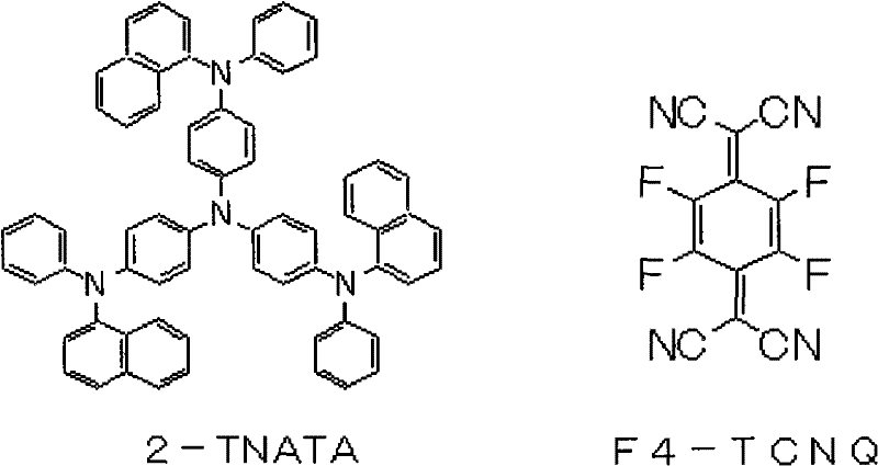
使用N,N’-二萘基-N,N’-二苯基-[1,1’-联苯基]-4,4’-二胺(缩写为“α-NPD”,参见下列结构式)在空穴注入层上形成10nm厚的空穴传输层。Use N,N'-dinaphthyl-N,N'-diphenyl-[1,1'-biphenyl]-4,4'-diamine (abbreviated as "α-NPD", see the following structural formula) A 10 nm thick hole transport layer was formed on the hole injection layer.

通过共蒸发1,3-双(咔唑-9-基)苯(缩写为“mCP”,参见下列结构式)和绿色发光材料三(2-苯基吡啶)铱(缩写为“Ir(ppy)3”,参见下列结构式)使得绿色发光材料的量是相对于mCP为5质量%而在空穴传输层上形成30nm厚的有机发光层。By
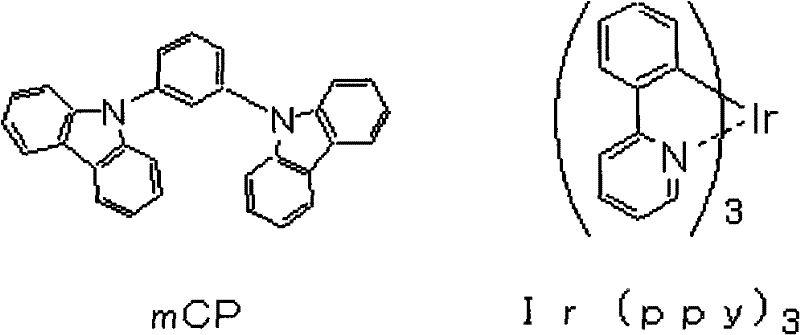
随后,使用双-(2-甲基-8-羟基喹啉)-4-(苯基苯酚)铝(缩写为“BAlq”,参见下列结构式)在有机发光层上形成40nm厚的电子传输层。Subsequently, a 40 nm-thick electron transport layer was formed on the organic light-emitting layer using bis-(2-methyl-8-hydroxyquinoline)-4-(phenylphenol)aluminum (abbreviated as "BAlq", see the following structural formula).

此外,使用阴影掩模(shadow mask)进行图案化以形成1nm厚的LiF层、2nm厚的Al层和100nm厚的ITO层。In addition, patterning was performed using a shadow mask to form a 1 nm thick LiF layer, a 2 nm thick Al layer, and a 100 nm thick ITO layer.
<密封层><sealing layer>
使用SiNx和SiOx的混合物在有机EL层上形成密封层。发现所述密封层的折射率为约1.8。A sealing layer is formed on the organic EL layer using a mixture of SiNx and SiOx . The sealing layer was found to have a refractive index of about 1.8.
(实施例2)(Example 2)
重复实施例1的过程,除了将中间层形成为使得折射率n4等于0.96n3而不是n3,从而制造实施例2的发光装置。The procedure of Example 1 was repeated except that the intermediate layer was formed such that the refractive index n 4 was equal to 0.96n 3 instead of n 3 , thereby manufacturing the light emitting device of Example 2.
(实施例3)(Example 3)
重复实施例1的过程,除了将中间层形成为使得折射率n4等于0.92n3而不是n3,从而制造实施例3的发光装置。The procedure of Example 1 was repeated except that the intermediate layer was formed such that the refractive index n 4 was equal to 0.92n 3 instead of n 3 , thereby manufacturing the light emitting device of Example 3.
(实施例4)(Example 4)
重复实施例1的过程,除了将中间层形成为使得折射率n4等于0.9n3而不是n3,从而制造实施例4的发光装置。The procedure of Example 1 was repeated except that the intermediate layer was formed such that the refractive index n 4 was equal to 0.9n 3 instead of n 3 , thereby manufacturing the light emitting device of Example 4.
(实施例5)(Example 5)
重复实施例1的过程,除了将中间层形成为使得折射率n4等于1.1n3而不是n3,从而制造实施例5的发光装置。The procedure of Example 1 was repeated except that the intermediate layer was formed such that the refractive index n 4 was equal to 1.1n 3 instead of n 3 , thereby manufacturing the light emitting device of Example 5.
(实施例6)(Example 6)
重复实施例1的过程,除了将精细凹凸图案形成为使得间距是0.15λ而不是0.6λ,从而制造实施例6的发光装置。The procedure of Example 1 was repeated except that the fine concavo-convex pattern was formed such that the pitch was 0.15λ instead of 0.6λ, thereby manufacturing the light emitting device of Example 6.
(实施例7)(Example 7)
重复实施例1的过程,除了将精细凹凸图案形成为使得间距是105λ而不是0.6λ,从而制造实施例7的发光装置。The procedure of Example 1 was repeated except that the fine concavo-convex pattern was formed such that the pitch was 105λ instead of 0.6λ, thereby manufacturing the light emitting device of Example 7.
(比较例1)(comparative example 1)
重复实施例1的过程,除了将中间层形成为使得折射率n4等于0.85n3而不是n3,从而制造比较例1的发光装置。The procedure of Example 1 was repeated except that the intermediate layer was formed such that the refractive index n 4 was equal to 0.85n 3 instead of n 3 , thereby manufacturing the light emitting device of Comparative Example 1.
(比较例2)(comparative example 2)
重复实施例1的过程,除了将中间层形成为使得折射率n4等于1.15n3而不是n3,从而制造比较例2的发光装置。The procedure of Example 1 was repeated except that the intermediate layer was formed such that the refractive index n 4 was equal to 1.15n 3 instead of n 3 , thereby manufacturing a light emitting device of Comparative Example 2.
<测量方法><measurement method>
<<折射率>><<Refractive Index>>
用椭圆计法测量有机EL层(发光部分)、中间层或密封层的折射率。The refractive index of the organic EL layer (light emitting portion), intermediate layer or sealing layer was measured by ellipsometer method.
<<精细凹凸图案的间距>><<Space of fine concave-convex pattern>>
用AFM(产品名称:OLS3500,是OLYMPUS CORPORATION的产品)测量精细凹凸图案的间距。The pitch of the fine concave-convex pattern was measured with an AFM (product name: OLS3500, a product of OLYMPUS CORPORATION).
<<光通量>><<Luminous flux>>
用多道光谱仪(Ocean Photonics,Inc.的产品)测量从制造的发光装置发射的光。Light emitted from the fabricated light-emitting device was measured with a multi-channel spectrometer (product of Ocean Photonics, Inc.).
特别地,用多道光谱仪(Ocean Photonics,Inc.的产品)测量从EL层(发光部分)发射的光的主发光波长。Specifically, the main emission wavelength of light emitted from the EL layer (light emitting portion) was measured with a multi-channel spectrometer (product of Ocean Photonics, Inc.).
<光提取效率的评价><Evaluation of Light Extraction Efficiency>
评价所制造的各个发光装置的光提取效率如下。The light extraction efficiency of each light-emitting device produced was evaluated as follows.
基于Q2/Q1比评价光提取效率,其中Q1表示没有精细凹凸图案的发光装置的光通量(即,将该值认为是1)且Q2表示实施例1到7和比较例1和2制造的各个发光装置的光通量。结果示于表1。The light extraction efficiency was evaluated based on the Q 2 /Q 1 ratio, where Q 1 represents the luminous flux of a light emitting device without a fine concavo-convex pattern (that is, the value is regarded as 1) and Q 2 represents Examples 1 to 7 and Comparative Examples 1 and 2 The luminous flux of each light-emitting device manufactured. The results are shown in Table 1.
表1Table 1

工业实用性Industrial Applicability
本发明的发光装置可以合适地用于例如显示装置、显示器(发光型平板显示器(有机EL、无机EL、等离子体))、背光、电子照相、照明光源、摄录光源、曝光光源、阅读光源、标识器、内部附件、光通信、LED和荧光管。The light-emitting device of the present invention can be suitably used in, for example, display devices, displays (light-emitting flat panel displays (organic EL, inorganic EL, plasma)), backlights, electrophotography, lighting sources, video recording light sources, exposure light sources, reading light sources, Markers, internal accessories, optical communications, LED and fluorescent tubes.
Claims (11)
Applications Claiming Priority (3)
| Application Number | Priority Date | Filing Date | Title |
|---|---|---|---|
| JP2008-243318 | 2008-09-22 | ||
| JP2008243318A JP5288967B2 (en) | 2008-09-22 | 2008-09-22 | LIGHT EMITTING ELEMENT, MANUFACTURING METHOD THEREOF, AND DISPLAY HAVING THE LIGHT EMITTING ELEMENT |
| PCT/JP2009/065620 WO2010032652A1 (en) | 2008-09-22 | 2009-09-02 | Light-emitting device, production method therefor, and display containing the same |
Publications (2)
| Publication Number | Publication Date |
|---|---|
| CN102160459A true CN102160459A (en) | 2011-08-17 |
| CN102160459B CN102160459B (en) | 2015-06-03 |
Family
ID=42039479
Family Applications (1)
| Application Number | Title | Priority Date | Filing Date |
|---|---|---|---|
| CN200980137205.1A Active CN102160459B (en) | 2008-09-22 | 2009-09-02 | Light-emitting device, method for producing light-emitting device, and display including same |
Country Status (6)
| Country | Link |
|---|---|
| US (1) | US8492783B2 (en) |
| EP (1) | EP2356881B1 (en) |
| JP (1) | JP5288967B2 (en) |
| CN (1) | CN102160459B (en) |
| TW (1) | TWI501688B (en) |
| WO (1) | WO2010032652A1 (en) |
Cited By (5)
| Publication number | Priority date | Publication date | Assignee | Title |
|---|---|---|---|---|
| CN104332561A (en) * | 2014-11-26 | 2015-02-04 | 京东方科技集团股份有限公司 | Organic light-emitting device, preparation method of organic light-emitting device and display device with organic light-emitting device |
| CN105304827A (en) * | 2015-11-02 | 2016-02-03 | 固安翌光科技有限公司 | OLED device |
| CN106338015A (en) * | 2015-07-08 | 2017-01-18 | 法雷奥照明公司 | Optical device, light module and lighting device comprising same |
| CN106931333A (en) * | 2011-11-23 | 2017-07-07 | 夸克星有限责任公司 | Light-emitting device |
| CN107833975A (en) * | 2016-08-31 | 2018-03-23 | 乐金显示有限公司 | White OLED and the display including white OLED |
Families Citing this family (11)
| Publication number | Priority date | Publication date | Assignee | Title |
|---|---|---|---|---|
| KR101874649B1 (en) | 2010-04-22 | 2018-07-04 | 이데미쓰 고산 가부시키가이샤 | Organic electroluminescent element and lighting device |
| JP2012204103A (en) * | 2011-03-24 | 2012-10-22 | Toshiba Corp | Organic electroluminescent element, display device and luminaire |
| CN103857440B (en) | 2011-06-22 | 2018-09-25 | 维奥姆生物科学有限公司 | Antimycotic and antibacterium prodrug based on conjugate |
| JPWO2013065177A1 (en) * | 2011-11-04 | 2015-04-02 | パイオニア株式会社 | Light emitting device |
| US20160128944A1 (en) | 2013-06-04 | 2016-05-12 | Vyome Biosciences Pvt. Ltd. | Coated particles and compositions comprising same |
| EA201691534A1 (en) | 2014-01-29 | 2016-12-30 | Вайоми Байосайенсиз Пвт. Лтд. | TREATMENT OF SUSTAINABLE UGRAI |
| US9761841B2 (en) * | 2014-04-24 | 2017-09-12 | Vitro, S.A.B. De C.V. | Organic light emitting diode with surface modification layer |
| WO2017010124A1 (en) * | 2015-07-15 | 2017-01-19 | コニカミノルタ株式会社 | Organic thin-film laminate and organic electroluminescence element |
| CA3010895A1 (en) | 2016-01-21 | 2017-07-27 | SeLux Diagnostics, Inc. | Methods for rapid antimicrobial susceptibility testing |
| US9834808B2 (en) | 2016-01-21 | 2017-12-05 | SeLux Diagnostics, Inc. | Methods for rapid antibiotic susceptibility testing |
| WO2018119439A1 (en) | 2016-12-23 | 2018-06-28 | SeLux Diagnostics, Inc. | Methods for improved rapid antimicrobial susceptibility testing |
Citations (3)
| Publication number | Priority date | Publication date | Assignee | Title |
|---|---|---|---|---|
| JP2006294491A (en) * | 2005-04-13 | 2006-10-26 | Seiko Epson Corp | ELECTROLUMINESCENT DEVICE, ELECTROLUMINESCENT DEVICE MANUFACTURING METHOD, ELECTRONIC DEVICE |
| CN101013734A (en) * | 2006-02-02 | 2007-08-08 | 三星电机株式会社 | Light emitting diode module |
| US20070205417A1 (en) * | 2006-03-02 | 2007-09-06 | Semiconductor Energy Laboratory Co., Ltd. | Light-emitting element, light-emitting device, lighting device, and electronic appliance |
Family Cites Families (16)
| Publication number | Priority date | Publication date | Assignee | Title |
|---|---|---|---|---|
| JP2991183B2 (en) | 1998-03-27 | 1999-12-20 | 日本電気株式会社 | Organic electroluminescence device |
| JP2001244066A (en) * | 2000-03-01 | 2001-09-07 | Seiko Epson Corp | Light emitting device |
| JP4984343B2 (en) | 2000-09-29 | 2012-07-25 | 株式会社日立製作所 | Organic electroluminescent device and optoelectronic device using the same |
| JP2004513483A (en) | 2000-11-02 | 2004-04-30 | スリーエム イノベイティブ プロパティズ カンパニー | Bright and contrast enhanced direct-view luminescent display |
| JP2003075621A (en) * | 2001-09-04 | 2003-03-12 | Dainippon Printing Co Ltd | Diffraction grating for authenticity certification and recording medium provided with the same |
| WO2003080764A1 (en) * | 2002-03-22 | 2003-10-02 | Nichia Corporation | Nitride phosphor and method for preparation thereof, and light emitting device |
| JP2005063838A (en) * | 2003-08-13 | 2005-03-10 | Toshiba Matsushita Display Technology Co Ltd | Optical device and organic EL display device |
| JP2005063839A (en) | 2003-08-13 | 2005-03-10 | Toshiba Matsushita Display Technology Co Ltd | Optical device and organic EL display device |
| US7450311B2 (en) * | 2003-12-12 | 2008-11-11 | Luminus Devices, Inc. | Optical display systems and methods |
| EP1566854A1 (en) * | 2004-02-19 | 2005-08-24 | Heptagon OY | Organic light emitting device |
| TWI229465B (en) * | 2004-03-02 | 2005-03-11 | Genesis Photonics Inc | Single chip white light component |
| JP3994287B2 (en) * | 2004-07-07 | 2007-10-17 | サンケン電気株式会社 | Semiconductor light emitting device |
| JP2006310721A (en) * | 2005-03-28 | 2006-11-09 | Yokohama National Univ | Self-luminous device |
| JP2008066027A (en) * | 2006-09-05 | 2008-03-21 | Fuji Electric Holdings Co Ltd | Substrate having uneven surface and organic EL device using the same |
| US7745843B2 (en) * | 2006-09-26 | 2010-06-29 | Stanley Electric Co., Ltd. | Semiconductor light emitting device |
| JP5008486B2 (en) * | 2007-07-19 | 2012-08-22 | キヤノン株式会社 | Display device |
-
2008
- 2008-09-22 JP JP2008243318A patent/JP5288967B2/en active Active
-
2009
- 2009-09-02 EP EP09814497.5A patent/EP2356881B1/en active Active
- 2009-09-02 CN CN200980137205.1A patent/CN102160459B/en active Active
- 2009-09-02 US US13/120,139 patent/US8492783B2/en active Active
- 2009-09-02 WO PCT/JP2009/065620 patent/WO2010032652A1/en not_active Ceased
- 2009-09-21 TW TW098131747A patent/TWI501688B/en active
Patent Citations (3)
| Publication number | Priority date | Publication date | Assignee | Title |
|---|---|---|---|---|
| JP2006294491A (en) * | 2005-04-13 | 2006-10-26 | Seiko Epson Corp | ELECTROLUMINESCENT DEVICE, ELECTROLUMINESCENT DEVICE MANUFACTURING METHOD, ELECTRONIC DEVICE |
| CN101013734A (en) * | 2006-02-02 | 2007-08-08 | 三星电机株式会社 | Light emitting diode module |
| US20070205417A1 (en) * | 2006-03-02 | 2007-09-06 | Semiconductor Energy Laboratory Co., Ltd. | Light-emitting element, light-emitting device, lighting device, and electronic appliance |
Non-Patent Citations (1)
| Title |
|---|
| SANO,H.等: "An Organic Light-Emitting Diode with Highly Effient Light Extraction Using Newly Developed Diffraction Layer", 《SID SYMPOSIUM DIGEST OF TECHNICAL PAPERS》 * |
Cited By (7)
| Publication number | Priority date | Publication date | Assignee | Title |
|---|---|---|---|---|
| CN106931333A (en) * | 2011-11-23 | 2017-07-07 | 夸克星有限责任公司 | Light-emitting device |
| CN104332561A (en) * | 2014-11-26 | 2015-02-04 | 京东方科技集团股份有限公司 | Organic light-emitting device, preparation method of organic light-emitting device and display device with organic light-emitting device |
| CN106338015A (en) * | 2015-07-08 | 2017-01-18 | 法雷奥照明公司 | Optical device, light module and lighting device comprising same |
| CN105304827A (en) * | 2015-11-02 | 2016-02-03 | 固安翌光科技有限公司 | OLED device |
| CN107833975A (en) * | 2016-08-31 | 2018-03-23 | 乐金显示有限公司 | White OLED and the display including white OLED |
| CN107833975B (en) * | 2016-08-31 | 2019-07-12 | 乐金显示有限公司 | White OLED and display including white OLED |
| US10431765B2 (en) | 2016-08-31 | 2019-10-01 | Lg Display Co., Ltd. | White organic light emitting diode and display including the same |
Also Published As
| Publication number | Publication date |
|---|---|
| WO2010032652A1 (en) | 2010-03-25 |
| EP2356881A1 (en) | 2011-08-17 |
| CN102160459B (en) | 2015-06-03 |
| EP2356881B1 (en) | 2017-12-06 |
| EP2356881A4 (en) | 2012-08-29 |
| US20110175116A1 (en) | 2011-07-21 |
| US8492783B2 (en) | 2013-07-23 |
| TWI501688B (en) | 2015-09-21 |
| JP2010073667A (en) | 2010-04-02 |
| JP5288967B2 (en) | 2013-09-11 |
| TW201018300A (en) | 2010-05-01 |
Similar Documents
| Publication | Publication Date | Title |
|---|---|---|
| CN102160459B (en) | Light-emitting device, method for producing light-emitting device, and display including same | |
| EP2356880B1 (en) | Light-emitting device, production method therefor, and display containing the same | |
| CN102187735B (en) | Light emitting element | |
| CN101901825B (en) | Organic electroluminescence device | |
| JP5427528B2 (en) | Optical member | |
| JP2010182449A (en) | Organic electroluminescent display device | |
| JP2009016579A (en) | Organic electroluminescence device and manufacturing method | |
| JP2011060549A (en) | Optical member for organic el device, and organic el device | |
| JP2010230714A (en) | Optical sheet and manufacturing method thereof | |
| JP4855286B2 (en) | Method for manufacturing organic electroluminescent device | |
| JP5610848B2 (en) | Organic electroluminescence device | |
| WO2011030882A1 (en) | Color filter and light-emitting display element | |
| JP5898398B2 (en) | Method for manufacturing organic electroluminescent light emitting device | |
| JP5427527B2 (en) | Organic light emitting display device and method for manufacturing organic light emitting display device | |
| JP2007157629A (en) | Organic electroluminescence device | |
| JP2010078813A (en) | Light emitting element, display with the light emitting element, and manufacturing method thereof | |
| JP2014013945A (en) | Organic electroluminescent element | |
| JP2008311076A (en) | Organic electroluminescent device and manufacturing method thereof | |
| JP2013020985A (en) | Organic el display device | |
| JP2010102918A (en) | Light-emitting element, and display equipped with light-emitting element |
Legal Events
| Date | Code | Title | Description |
|---|---|---|---|
| C06 | Publication | ||
| PB01 | Publication | ||
| C10 | Entry into substantive examination | ||
| SE01 | Entry into force of request for substantive examination | ||
| ASS | Succession or assignment of patent right |
Owner name: UDC IRELAND INC. Free format text: FORMER OWNER: FUJI FILM CORP. Effective date: 20130207 |
|
| C41 | Transfer of patent application or patent right or utility model | ||
| TA01 | Transfer of patent application right |
Effective date of registration: 20130207 Address after: Dublin, Ireland Applicant after: UDC Ireland Ltd. Address before: Tokyo, Japan Applicant before: Fuji Film Corp. |
|
| C14 | Grant of patent or utility model | ||
| GR01 | Patent grant |