WO2024171715A1 - Plasma processing device - Google Patents
Plasma processing device Download PDFInfo
- Publication number
- WO2024171715A1 WO2024171715A1 PCT/JP2024/001422 JP2024001422W WO2024171715A1 WO 2024171715 A1 WO2024171715 A1 WO 2024171715A1 JP 2024001422 W JP2024001422 W JP 2024001422W WO 2024171715 A1 WO2024171715 A1 WO 2024171715A1
- Authority
- WO
- WIPO (PCT)
- Prior art keywords
- plasma processing
- pulsed
- disposed
- bias electrode
- signal
- Prior art date
- Legal status (The legal status is an assumption and is not a legal conclusion. Google has not performed a legal analysis and makes no representation as to the accuracy of the status listed.)
- Ceased
Links
Images
Classifications
-
- H—ELECTRICITY
- H01—ELECTRIC ELEMENTS
- H01J—ELECTRIC DISCHARGE TUBES OR DISCHARGE LAMPS
- H01J37/00—Discharge tubes with provision for introducing objects or material to be exposed to the discharge, e.g. for the purpose of examination or processing thereof
- H01J37/32—Gas-filled discharge tubes
- H01J37/32431—Constructional details of the reactor
- H01J37/32532—Electrodes
- H01J37/32568—Relative arrangement or disposition of electrodes; moving means
-
- H—ELECTRICITY
- H01—ELECTRIC ELEMENTS
- H01J—ELECTRIC DISCHARGE TUBES OR DISCHARGE LAMPS
- H01J37/00—Discharge tubes with provision for introducing objects or material to be exposed to the discharge, e.g. for the purpose of examination or processing thereof
- H01J37/32—Gas-filled discharge tubes
- H01J37/32009—Arrangements for generation of plasma specially adapted for examination or treatment of objects, e.g. plasma sources
- H01J37/32082—Radio frequency generated discharge
- H01J37/32137—Radio frequency generated discharge controlling of the discharge by modulation of energy
- H01J37/32146—Amplitude modulation, includes pulsing
-
- H—ELECTRICITY
- H01—ELECTRIC ELEMENTS
- H01J—ELECTRIC DISCHARGE TUBES OR DISCHARGE LAMPS
- H01J37/00—Discharge tubes with provision for introducing objects or material to be exposed to the discharge, e.g. for the purpose of examination or processing thereof
- H01J37/32—Gas-filled discharge tubes
- H01J37/32009—Arrangements for generation of plasma specially adapted for examination or treatment of objects, e.g. plasma sources
- H01J37/32082—Radio frequency generated discharge
- H01J37/32174—Circuits specially adapted for controlling the RF discharge
-
- H—ELECTRICITY
- H01—ELECTRIC ELEMENTS
- H01J—ELECTRIC DISCHARGE TUBES OR DISCHARGE LAMPS
- H01J37/00—Discharge tubes with provision for introducing objects or material to be exposed to the discharge, e.g. for the purpose of examination or processing thereof
- H01J37/32—Gas-filled discharge tubes
- H01J37/32431—Constructional details of the reactor
- H01J37/32532—Electrodes
- H01J37/32577—Electrical connecting means
-
- H—ELECTRICITY
- H01—ELECTRIC ELEMENTS
- H01J—ELECTRIC DISCHARGE TUBES OR DISCHARGE LAMPS
- H01J37/00—Discharge tubes with provision for introducing objects or material to be exposed to the discharge, e.g. for the purpose of examination or processing thereof
- H01J37/32—Gas-filled discharge tubes
- H01J37/32431—Constructional details of the reactor
- H01J37/32623—Mechanical discharge control means
- H01J37/32642—Focus rings
-
- H—ELECTRICITY
- H01—ELECTRIC ELEMENTS
- H01J—ELECTRIC DISCHARGE TUBES OR DISCHARGE LAMPS
- H01J37/00—Discharge tubes with provision for introducing objects or material to be exposed to the discharge, e.g. for the purpose of examination or processing thereof
- H01J37/32—Gas-filled discharge tubes
- H01J37/32431—Constructional details of the reactor
- H01J37/32715—Workpiece holder
-
- H—ELECTRICITY
- H05—ELECTRIC TECHNIQUES NOT OTHERWISE PROVIDED FOR
- H05H—PLASMA TECHNIQUE; PRODUCTION OF ACCELERATED ELECTRICALLY-CHARGED PARTICLES OR OF NEUTRONS; PRODUCTION OR ACCELERATION OF NEUTRAL MOLECULAR OR ATOMIC BEAMS
- H05H1/00—Generating plasma; Handling plasma
- H05H1/24—Generating plasma
- H05H1/46—Generating plasma using applied electromagnetic fields, e.g. high frequency or microwave energy
-
- H—ELECTRICITY
- H10—SEMICONDUCTOR DEVICES; ELECTRIC SOLID-STATE DEVICES NOT OTHERWISE PROVIDED FOR
- H10P—GENERIC PROCESSES OR APPARATUS FOR THE MANUFACTURE OR TREATMENT OF DEVICES COVERED BY CLASS H10
- H10P50/00—Etching of wafers, substrates or parts of devices
- H10P50/20—Dry etching; Plasma etching; Reactive-ion etching
- H10P50/24—Dry etching; Plasma etching; Reactive-ion etching of semiconductor materials
- H10P50/242—Dry etching; Plasma etching; Reactive-ion etching of semiconductor materials of Group IV materials
-
- H—ELECTRICITY
- H10—SEMICONDUCTOR DEVICES; ELECTRIC SOLID-STATE DEVICES NOT OTHERWISE PROVIDED FOR
- H10P—GENERIC PROCESSES OR APPARATUS FOR THE MANUFACTURE OR TREATMENT OF DEVICES COVERED BY CLASS H10
- H10P72/00—Handling or holding of wafers, substrates or devices during manufacture or treatment thereof
- H10P72/70—Handling or holding of wafers, substrates or devices during manufacture or treatment thereof for supporting or gripping
- H10P72/72—Handling or holding of wafers, substrates or devices during manufacture or treatment thereof for supporting or gripping using electrostatic chucks
-
- H—ELECTRICITY
- H01—ELECTRIC ELEMENTS
- H01J—ELECTRIC DISCHARGE TUBES OR DISCHARGE LAMPS
- H01J2237/00—Discharge tubes exposing object to beam, e.g. for analysis treatment, etching, imaging
- H01J2237/20—Positioning, supporting, modifying or maintaining the physical state of objects being observed or treated
- H01J2237/2007—Holding mechanisms
Definitions
- An exemplary embodiment of the present disclosure relates to a plasma processing apparatus.
- Patent Document 1 a technology for performing plasma processing using a pulse voltage is described in Patent Document 1.
- This disclosure provides a technique for properly performing plasma processing using a pulsed DC signal.
- the plasma processing apparatus includes a plasma processing chamber, a substrate support disposed within the plasma processing chamber, the substrate support including a conductive base, an electrostatic chuck disposed on the conductive base, a chuck electrode disposed within the electrostatic chuck, and a bias electrode disposed below the chuck electrode within the electrostatic chuck, an upper electrode disposed above the substrate support, an RF generating unit electrically connected to the conductive base, the bias electrode, or the upper electrode and configured to generate an RF signal, a pulsed DC generating unit electrically connected to the bias electrode and configured to generate a pulsed DC signal, an RF filter connected between the bias electrode and the pulsed DC generating unit, and a ringing suppression circuit connected between the bias electrode and the pulsed DC generating unit and configured to suppress ringing superimposed on the pulsed DC signal.
- a technique can be provided for properly performing plasma processing using a pulsed DC signal.
- FIG. 1 is a diagram for explaining a configuration example of a plasma processing system.
- FIG. 1 is a diagram for explaining a configuration example of a capacitively coupled plasma processing apparatus.
- 3A and 3B are diagrams illustrating an example of the configuration of a substrate support and a power supply in the first exemplary embodiment.
- FIG. 2 is a diagram illustrating a configuration example of a first ringing suppression circuit;
- FIG. 4 illustrates an example of a sequence of first voltage pulses.
- FIG. 13 is a diagram showing the results of measuring the substrate potential on an electrostatic chuck to which a pulsed DC signal is applied, in cases where a ferrite core is disposed as a ringing suppression circuit between a pulsed DC generating unit and a substrate bias electrode, and in cases where a ferrite core is not disposed.
- FIG. 13 is a diagram showing an ion energy distribution function on a substrate during plasma processing in the absence of a ferrite core.
- FIG. 13 is a diagram showing an ion energy distribution function on a substrate during plasma processing in the presence of a ferrite core.
- FIG. 13 is a diagram showing the results of measuring the etching rate of a substrate in an etching process when a ferrite core is present and when a ferrite core is not present.
- FIG. 2 is a diagram showing a configuration example of a first ringing suppression circuit having a plurality of conductors;
- FIG. 13 is a diagram showing an example of the configuration of a substrate support and a power supply in a second exemplary embodiment.
- FIG. 13 is a diagram illustrating a configuration example of a second ringing suppression circuit.
- FIG. 11 is a diagram showing an example of a sequence of second voltage pulses.
- a plasma processing apparatus in one exemplary embodiment, includes a plasma processing chamber, a substrate support disposed within the plasma processing chamber, the substrate support including a conductive base, an electrostatic chuck disposed on the conductive base, a chuck electrode disposed within the electrostatic chuck, and a bias electrode disposed below the chuck electrode within the electrostatic chuck, an upper electrode disposed above the substrate support, an RF generator electrically connected to the conductive base, the bias electrode, or the upper electrode and configured to generate an RF signal, a pulsed DC generator electrically connected to the bias electrode and configured to generate a pulsed DC signal, an RF filter connected between the bias electrode and the pulsed DC generator, and a ringing suppression circuit connected between the bias electrode and the pulsed DC generator and configured to suppress ringing superimposed on the pulsed DC signal.
- the ringing suppression circuit includes at least one ferrite core.
- the ringing suppression circuit includes a plurality of conductors connected in parallel and a plurality of ferrite cores, at least one of which is disposed on each of the plurality of conductors.
- the pulsed DC signal comprises a sequence of voltage pulses.
- the sequence of voltage pulses has negative polarity voltage levels.
- the sequence of voltage pulses has a pulse frequency in the range of 100 kHz to 1 MHz.
- the pulsed DC signal has a sequence of voltage pulses having a first voltage level during a first period in each cycle and a second voltage level during a second period in each cycle, the absolute value of the first voltage level being greater than the absolute value of the second voltage level.
- the first voltage level has a negative polarity.
- the sequence of voltage pulses has a pulse frequency in the range of 100 kHz to 1 MHz.
- the second voltage level has a zero voltage level.
- a plasma processing chamber and a substrate support disposed within the plasma processing chamber including a base, an electrostatic chuck disposed on the base and having a substrate support surface and an edge ring support surface, an edge ring disposed on the edge ring support surface to surround a substrate on the substrate support surface, a substrate bias electrode disposed within the electrostatic chuck below the substrate support surface, and an edge ring bias electrode disposed within the electrostatic chuck below the edge ring support surface
- the substrate support including a base, an RF generating unit configured to generate an RF signal for generating a plasma within the plasma processing chamber, and a first pulsed DC generating unit electrically connected to the substrate bias electrode and configured to generate a first pulsed DC signal.
- a plasma processing apparatus includes a first RF filter connected between a substrate bias electrode and a first pulsed DC generation unit, a first ringing suppression circuit connected between the substrate bias electrode and the first pulsed DC generation unit and configured to suppress ringing superimposed on the first pulsed DC signal, a second pulsed DC generation unit electrically connected to the edge ring bias electrode and configured to generate a second pulsed DC signal, a second RF filter connected between the edge ring bias electrode and the second pulsed DC generation unit, and a second ringing suppression circuit connected between the edge ring bias electrode and the second pulsed DC generation unit and configured to suppress ringing superimposed on the second pulsed DC signal.
- the first ringing suppression circuit includes at least one first ferrite core.
- the second ringing suppression circuit includes at least one second ferrite core.
- the second ringing suppression circuit includes a plurality of second conductors connected in parallel and a plurality of second ferrite cores, at least one of which is disposed on each of the plurality of second conductors.
- the first ringing suppression circuit includes a plurality of first conductors connected in parallel and a plurality of first ferrite cores, at least one of which is disposed on each of the plurality of first conductors.
- the second ringing suppression circuit includes at least one second ferrite core.
- the second ringing suppression circuit includes a plurality of second conductors connected in parallel and a plurality of second ferrite cores, at least one of which is disposed on each of the plurality of second conductors.
- a plasma processing apparatus in one exemplary embodiment, includes a plasma processing chamber, a substrate support disposed within the plasma processing chamber, the substrate support including a base, an electrostatic chuck disposed on the base, and a bias electrode disposed within the electrostatic chuck, an RF generator configured to generate an RF signal for generating plasma within the plasma processing chamber, a pulsed DC generator electrically connected to the bias electrode and configured to generate a pulsed DC signal, and a ringing suppression circuit connected between the bias electrode and the pulsed DC generator and configured to suppress ringing occurring between a first parasitic capacitor and a second parasitic capacitor from being superimposed on the pulsed DC signal, the first parasitic capacitor occurring between the bias electrode and a ground potential, and the second parasitic capacitor occurring between a node on a path from the pulsed DC generator to the bias electrode and the ground potential.
- the ringing suppression circuit includes at least one ferrite core.
- the ringing suppression circuit includes a plurality of conductors connected in parallel and a plurality of ferrite cores, at least one of which is disposed on each of the plurality of conductors.
- FIG. 1 is a diagram for explaining a configuration example of a plasma processing system.
- the plasma processing system includes a plasma processing device 1 and a control unit 2.
- the plasma processing system is an example of a substrate processing system
- the plasma processing device 1 is an example of a substrate processing device.
- the plasma processing device 1 includes a plasma processing chamber 10, a substrate support unit 11, and a plasma generation unit 12.
- the plasma processing chamber 10 has a plasma processing space.
- the plasma processing chamber 10 also has at least one gas supply port for supplying at least one processing gas to the plasma processing space, and at least one gas exhaust port for exhausting gas from the plasma processing space.
- the gas supply port is connected to a gas supply unit 20 described later, and the gas exhaust port is connected to an exhaust system 40 described later.
- the substrate support unit 11 is disposed in the plasma processing space, and has a substrate support surface for supporting a substrate.
- the plasma generating unit 12 is configured to generate plasma from at least one processing gas supplied into the plasma processing space.
- the plasma formed in the plasma processing space may be capacitively coupled plasma (CCP), inductively coupled plasma (ICP), ECR plasma (Electron-Cyclotron-resonance plasma), Helicon wave excited plasma (HWP), or surface wave plasma (SWP), etc.
- various types of plasma generating units may be used, including AC (Alternating Current) plasma generating units and DC (Direct Current) plasma generating units.
- the AC signal (AC power) used in the AC plasma generating unit has a frequency in the range of 100 kHz to 10 GHz.
- AC signals include RF (Radio Frequency) signals and microwave signals.
- the RF signal has a frequency in the range of 100 kHz to 150 MHz.
- the control unit 2 processes computer-executable instructions that cause the plasma processing apparatus 1 to perform the various steps described in this disclosure.
- the control unit 2 may be configured to control each element of the plasma processing apparatus 1 to perform the various steps described herein. In one embodiment, a part or all of the control unit 2 may be included in the plasma processing apparatus 1.
- the control unit 2 may include, for example, a computer 2a.
- the computer 2a may include, for example, a processing unit (CPU: Central Processing Unit) 2a1, a storage unit 2a2, and a communication interface 2a3.
- the processing unit 2a1 may be configured to perform various control operations by reading a program from the storage unit 2a2 and executing the read program. This program may be stored in the storage unit 2a2 in advance, or may be acquired via a medium when necessary.
- the acquired program is stored in the storage unit 2a2, and is read from the storage unit 2a2 by the processing unit 2a1 and executed.
- the medium may be various storage media readable by the computer 2a, or may be a communication line connected to the communication interface 2a3.
- the memory unit 2a2 may include a RAM (Random Access Memory), a ROM (Read Only Memory), a HDD (Hard Disk Drive), a SSD (Solid State Drive), or a combination of these.
- the communication interface 2a3 may communicate with the plasma processing device 1 via a communication line such as a LAN (Local Area Network).
- FIG. 1 is a diagram for explaining a configuration example of a capacitively coupled plasma processing device.
- the capacitively coupled plasma processing apparatus 1 includes a plasma processing chamber 10, a gas supply unit 20, a power supply 30, and an exhaust system 40.
- the plasma processing apparatus 1 also includes a substrate support unit 11 and a gas inlet unit.
- the gas inlet unit is configured to introduce at least one processing gas into the plasma processing chamber 10.
- the gas inlet unit includes a shower head 13.
- the substrate support unit 11 is disposed in the plasma processing chamber 10.
- the shower head 13 is disposed above the substrate support unit 11. In one embodiment, the shower head 13 constitutes at least a part of the ceiling of the plasma processing chamber 10.
- the plasma processing chamber 10 has a plasma processing space 10s defined by the shower head 13, the sidewall 10a of the plasma processing chamber 10, and the substrate support unit 11.
- the plasma processing chamber 10 is grounded.
- the shower head 13 and the substrate support unit 11 are electrically insulated from the housing of the plasma processing chamber 10.
- the substrate support 11 includes a main body 111 and a ring assembly 112.
- the main body 111 has a central region 111a for supporting the substrate W and an annular region 111b for supporting the ring assembly 112.
- a wafer is an example of a substrate W.
- the annular region 111b of the main body 111 surrounds the central region 111a of the main body 111 in a plan view.
- the substrate W is disposed on the central region 111a of the main body 111
- the ring assembly 112 is disposed on the annular region 111b of the main body 111 so as to surround the substrate W on the central region 111a of the main body 111. Therefore, the central region 111a is also called a substrate support surface for supporting the substrate W, and the annular region 111b is also called an edge ring support surface for supporting the ring assembly 112.
- the main body 111 includes a base 1110 and an electrostatic chuck 1111.
- the base 1110 includes a conductive member and can be a conductive base.
- the conductive member of the base 1110 can function as a lower electrode.
- the electrostatic chuck 1111 is disposed on the base 1110.
- the electrostatic chuck 1111 includes a ceramic member 1111a and an electrostatic electrode (chuck electrode) 1111b disposed within the ceramic member 1111a.
- the ceramic member 1111a has a central region 111a. In one embodiment, the ceramic member 1111a also has an annular region 111b. Note that other members surrounding the electrostatic chuck 1111, such as an annular electrostatic chuck or an annular insulating member, may have the annular region 111b.
- the ring assembly 112 may be disposed on the annular electrostatic chuck or the annular insulating member, or may be disposed on both the electrostatic chuck 1111 and the annular insulating member.
- an RF or DC electrode may be disposed within the ceramic member 1111a, in which case the RF or DC electrode functions as the lower electrode.
- the RF or DC electrode is also called a bias electrode. Note that both the conductive member of the base 1110 and the RF or DC electrode may function as two lower electrodes.
- the ring assembly 112 includes one or more annular members.
- the one or more annular members include one or more edge rings and at least one cover ring.
- the edge rings are formed of a conductive or insulating material, and the cover rings are formed of an insulating material.
- the substrate support 11 may also include a temperature adjustment module configured to adjust at least one of the electrostatic chuck 1111, the ring assembly 112, and the substrate to a target temperature.
- the temperature adjustment module may include a heater, a heat transfer medium, a flow passage 1110a, or a combination thereof.
- a heat transfer fluid such as brine or a gas flows through the flow passage 1110a.
- the flow passage 1110a is formed in the base 1110, and one or more heaters are disposed in the ceramic member 1111a of the electrostatic chuck 1111.
- the substrate support 11 may also include a heat transfer gas supply configured to supply a heat transfer gas between the back surface of the substrate W and the central region 111a.
- the shower head 13 is configured to introduce at least one processing gas from the gas supply unit 20 into the plasma processing space 10s.
- the shower head 13 has at least one gas supply port 13a, at least one gas diffusion chamber 13b, and multiple gas inlets 13c.
- the processing gas supplied to the gas supply port 13a passes through the gas diffusion chamber 13b and is introduced into the plasma processing space 10s from the multiple gas inlets 13c.
- the shower head 13 also includes an upper electrode.
- the gas introduction unit may include, in addition to the shower head 13, one or more side gas injectors (SGI) attached to one or more openings formed in the side wall 10a.
- SGI side gas injectors
- the gas supply unit 20 may include at least one gas source 21 and at least one flow controller 22.
- the gas supply unit 20 is configured to supply at least one process gas from a respective gas source 21 through a respective flow controller 22 to the showerhead 13.
- Each flow controller 22 may include, for example, a mass flow controller or a pressure-controlled flow controller.
- the gas supply unit 20 may include at least one flow modulation device that modulates or pulses the flow rate of the at least one process gas.
- the power supply 30 includes an RF power supply 31 coupled to the plasma processing chamber 10 via at least one impedance matching circuit.
- the RF power supply 31 is configured to supply at least one RF signal (RF power), such as a source RF signal and a bias RF signal, to at least one lower electrode and/or at least one upper electrode. This causes a plasma to be formed from at least one processing gas supplied to the plasma processing space 10s.
- the RF power supply 31 can function as at least a part of the plasma generating unit 12.
- a bias RF signal to at least one lower electrode, a bias potential is generated on the substrate W, and ion components in the formed plasma can be attracted to the substrate W.
- the RF power supply 31 includes a first RF generating unit 31a and a second RF generating unit 31b.
- the first RF generating unit 31a is coupled to at least one lower electrode and/or at least one upper electrode via at least one impedance matching circuit and configured to generate a source RF signal (source RF power) for plasma generation.
- the source RF signal has a frequency in the range of 10 MHz to 150 MHz.
- the first RF generating unit 31a may be configured to generate multiple source RF signals having different frequencies. The generated one or more source RF signals are supplied to at least one lower electrode and/or at least one upper electrode.
- the second RF generator 31b is coupled to at least one lower electrode via at least one impedance matching circuit and configured to generate a bias RF signal (bias RF power).
- the frequency of the bias RF signal may be the same as or different from the frequency of the source RF signal.
- the bias RF signal has a frequency lower than the frequency of the source RF signal.
- the bias RF signal has a frequency in the range of 100 kHz to 60 MHz.
- the second RF generator 31b may be configured to generate multiple bias RF signals having different frequencies.
- the generated one or more bias RF signals are provided to at least one lower electrode. Also, in various embodiments, at least one of the source RF signal and the bias RF signal may be pulsed.
- the power supply 30 may also include a DC power supply 32 coupled to the plasma processing chamber 10.
- the DC power supply 32 includes a first DC generator 32a and a second DC generator 32b.
- the first DC generator 32a is connected to at least one lower electrode and configured to generate a first DC signal.
- the generated first DC signal is applied to the at least one lower electrode.
- the second DC generator 32b is connected to at least one upper electrode and configured to generate a second DC signal.
- the generated second DC signal is applied to the at least one upper electrode.
- the first and second DC signals may be pulsed.
- a sequence of DC-based voltage pulses is applied to at least one lower electrode and/or at least one upper electrode.
- the voltage pulses may have a rectangular, trapezoidal, triangular or combination of these pulse waveforms.
- a waveform generator for generating a sequence of voltage pulses from the DC signal is connected between the first DC generator 32a and at least one lower electrode.
- the first DC generator 32a and the waveform generator constitute a voltage pulse generator.
- the second DC generator 32b and the waveform generator constitute a voltage pulse generator
- the voltage pulse generator is connected to at least one upper electrode.
- the voltage pulses may have a positive polarity or a negative polarity.
- the sequence of voltage pulses may include one or more positive polarity voltage pulses and one or more negative polarity voltage pulses within one period.
- the first and second DC generating units 32a and 32b may be provided in addition to the RF power source 31, or the first DC generating unit 32a may be provided in place of the second RF generating unit 31b.
- the exhaust system 40 may be connected to, for example, a gas exhaust port 10e provided at the bottom of the plasma processing chamber 10.
- the exhaust system 40 may include a pressure regulating valve and a vacuum pump. The pressure in the plasma processing space 10s is adjusted by the pressure regulating valve.
- the vacuum pump may include a turbomolecular pump, a dry pump, or a combination thereof.
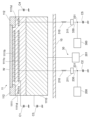
- First Exemplary Embodiment 3 shows an example of the configuration of the substrate support 11 and the power supply 30 in the first exemplary embodiment.
- the substrate support 11 has a chuck electrode 1111b and a substrate bias electrode 1111c inside the electrostatic chuck 1111.
- the substrate bias electrode 1111c may be disposed below the chuck electrode 1111b.
- a first pulsed DC generator 200 that generates a first pulsed DC signal is electrically connected to the substrate bias electrode 1111c.
- the first pulsed DC generator 200 may be an example of the first DC generator 32a described above.
- An RF generator 201 that generates an RF signal is electrically connected to the base 1110.
- the RF generator 201 may be an example of the first RF generator 31a and/or the second RF generator 31b described above.
- the RF generator 201 may be connected to the substrate bias electrode 1111c.
- a first RF filter 210 and a first ringing suppression circuit 211 are connected between the substrate bias electrode 1111c and the first pulsed DC generating unit 200.
- the substrate bias electrode 1111c is grounded, and a first parasitic capacitor C1 may be generated between the substrate bias electrode 1111c and the ground potential.
- a path 230 from the first pulsed DC generating unit 200 to the substrate bias electrode 1111c is grounded, and a second parasitic capacitor C2 may be generated between a node 231 on the path 230 and the ground potential.
- the base 1110 is grounded, and a third parasitic capacitor 3 may be generated between the base 1110 and the ground potential.
- the first RF filter 210 is configured to suppress the RF signal supplied from the RF generating unit 201 to the base 1110 from entering the first pulsed DC generating unit 200 via the path 230.
- the first RF filter 210 may remove signals of a specific frequency depending on the frequency of the RF signal.
- the first RF filter 210 may be a coil.
- the first RF filter 210 may be disposed outside the chamber 10.
- the first ringing suppression circuit 211 is configured to suppress ringing superimposed on the first pulsed DC signal.
- the first ringing suppression circuit 211 may be provided outside the chamber 10.
- the first ringing suppression circuit 211 may be connected between the first RF filter 210 and the first pulsed DC generating unit 200.
- the first ringing suppression circuit 211 may be connected between the first RF filter 210 and the substrate bias electrode 1111c.
- the first ringing suppression circuit 211 includes a first conductor 250 connected to the path 230 and a first ferrite core 251 disposed on the first conductor 250.
- the first ferrite core 251 can remove ringing superimposed on the first pulse DC signal.
- the first pulsed DC signal of the first pulsed DC generator 200 has a sequence of voltage pulses.
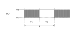
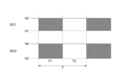
- FIG. 5 shows an example of a first sequence of voltage pulses DC1 generated by the first pulsed DC generator 200.
- the first sequence of voltage pulses DC1 has a pulse frequency in the range of 100 kHz to 1 MHz.
- the first sequence of voltage pulses DC1 has a repeating cycle T.
- the first sequence of voltage pulses DC1 may have a first voltage level V1 in a first period T1 in each cycle T and a second voltage level V2, which is a reference voltage level, in a second period T2 of each cycle T.
- the absolute value of the first voltage level V1 is greater than the absolute value of the second voltage level V2.
- the first voltage level V1 has a negative polarity.
- the second voltage level V2 has a zero voltage level.
- the first voltage level V1 is 0V to -15kV.
- the plasma processing performed by using the plasma processing apparatus 1 includes an etching process in which plasma is used to etch a film on the substrate W.
- the plasma processing is executed by the control unit 2.
- the substrate W is carried into the chamber 10 by the transport arm, placed on the substrate support 11 by the lifter, and held by suction on the substrate support 11 as shown in FIG. 2.
- the processing gas is supplied to the shower head 13 by the gas supply unit 20, and is supplied from the shower head 13 to the plasma processing space 10s.
- the processing gas supplied at this time includes a gas that generates active species necessary for the etching process of the substrate W.
- a source RF signal for generating plasma is supplied to the lower electrode and/or the upper electrode.
- a bias signal for attracting ions may be supplied to the lower electrode.
- the atmosphere in the plasma processing space 10s may be exhausted from the gas exhaust port 10e, and the pressure in the plasma processing space 10s may be reduced to a predetermined pressure. As a result, plasma is generated in the plasma processing space 10s, and the substrate W is etched.
- an RF signal is supplied to the base 1110 shown in FIG. 3 by the RF generating unit 201.
- a first pulsed DC signal is applied as a bias signal to the substrate bias electrode 1111c by the first pulsed DC generating unit 200.
- the first RF filter 210 prevents the RF signal supplied from the RF generating unit 201 to the base 1110 from entering the first pulsed DC generating unit 200 via the path 230.
- the first ringing suppression circuit 211 prevents ringing occurring between the first parasitic capacitor C1 and the second parasitic capacitor C2 from being superimposed on the first pulsed DC signal.
- the plasma processing apparatus 1 includes a base 1110, an RF generating unit 201, a first pulsed DC generating unit 200, a first RF filter 210, and a first ringing suppression circuit 211.
- This makes it possible to suppress ringing from being superimposed on the pulsed DC signal applied from the first pulsed DC generating unit 200 to the substrate bias electrode 1111c. Therefore, plasma processing using the pulsed DC signal can be performed appropriately.
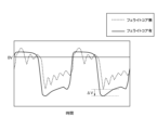
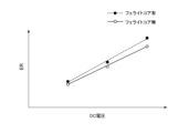
- Example 6 The substrate potential on the electrostatic chuck to which the pulsed DC signal was applied was measured for the case where a ferrite core was arranged as a ringing suppression circuit between the pulsed DC generating unit and the substrate bias electrode (with ferrite core) and the case where a ferrite core was not arranged (without ferrite core).
- FIG. 6 shows the measurement results.
- the substrate potential in the case where the ferrite core is present is closer to the rectangular waveform of the pulsed DC signal than in the case where the ferrite core is not present, and it can be confirmed that the ringing (high frequency component) superimposed on the pulsed DC signal is reduced.
- the absolute value of the substrate potential in the case where the ferrite core is present is higher than that in the case where the ferrite core is not present ( ⁇ V in FIG. 6). This makes it possible to confirm that the electric energy of the pulsed DC signal is efficiently transmitted to the substrate in the case where the ferrite core is present.
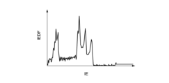
- Figure 7 shows the ion energy distribution function (IEDF) on a substrate during plasma processing when there is no ferrite core.
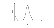
- Figure 8 shows the ion energy distribution function on a substrate during plasma processing when there is a ferrite core. It can be seen that when there is no ferrite core, there are multiple peaks in the ion energy distribution function in the high ion energy (IE) region, whereas when there is a ferrite core, there is only one peak in the high ion energy (IE) region. This shows that when there is a ferrite core, the ion energy on the substrate is high and stable.
- IEDF ion energy distribution function
- Figure 9 shows the results of measuring the etching rate (ER) of a substrate during etching processing with and without a ferrite core.
- the horizontal axis of Figure 9 is the DC voltage of the pulsed DC signal. It can be seen that the etching rate with a ferrite core is higher than that without a ferrite core.
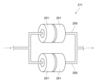
- the first ringing suppression circuit 211 may have a plurality of first conductors 250 connected in parallel, and a plurality of first ferrite cores 251 arranged on each of the plurality of first conductors 250, as shown in FIG. 10.
- each first conductor 250 may have a plurality of first ferrite cores 251 arranged thereon, or may have one first ferrite core 251 arranged thereon. In such a case, the current flowing through each first conductor 250 is reduced by the pulsed DC signal, and as a result, the heat generation of the first ferrite core 251 caused by removing the ringing can be suppressed.
- Second Exemplary Embodiment 11 shows an example of the configuration of the substrate support 11 and the power supply 30 in the second exemplary embodiment.
- the substrate support 11 may have an edge ring bias electrode 1111d in addition to the chuck electrode 1111b and the substrate bias electrode 1111c inside the electrostatic chuck 1111.
- the edge ring bias electrode 1111d may be disposed below the edge ring support surface.
- a second pulsed DC generator 300 that generates a second pulsed DC signal is electrically connected to the edge ring bias electrode 1111d.
- a second RF filter 310 and a second ringing suppression circuit 311 are connected between the edge ring bias electrode 1111d and the second pulsed DC generating unit 300.
- the edge ring bias electrode 1111d is grounded, and a fourth parasitic capacitor C4 may be generated between the edge ring bias electrode 1111d and the ground potential.
- a path 330 from the second pulsed DC generating unit 300 to the edge ring bias electrode 1111d is grounded, and a fifth parasitic capacitor C5 may be generated between a node 331 on the path 330 and the ground potential.
- the second RF filter 310 is configured to suppress the RF signal supplied from the RF generating unit 201 to the base 1110 from entering the second pulsed DC generating unit 300 via the path 330.
- the second RF filter 310 may remove signals of a specific frequency depending on the frequency of the RF signal.
- the second RF filter 310 may be a coil.
- the second RF filter 310 may be provided outside the chamber 10.
- the second ringing suppression circuit 311 is configured to suppress ringing superimposed on the second pulsed DC signal.
- the second ringing suppression circuit 311 may be provided outside the chamber 10.
- the second ringing suppression circuit 311 may be connected between the second RF filter 310 and the second pulsed DC generation unit 300.
- the second ringing suppression circuit 311 may be connected between the second RF filter 310 and the edge ring bias electrode 1111d.
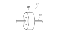
- the second ringing suppression circuit 311 includes a second conductor 350 connected to the path 330 and a second ferrite core 351 arranged on the second conductor 350.
- Each second conductor 350 may have multiple second ferrite cores 351 arranged thereon, or may have one second ferrite core 351 arranged thereon.
- the second ferrite core 351 can remove ringing superimposed on the second pulse DC signal.
- the second pulsed DC signal of the second pulsed DC generating unit 300 has a sequence of voltage pulses.
- FIG. 13 shows an example of the second sequence of voltage pulses DC2 generated by the second pulsed DC generating unit 300.
- the second sequence of voltage pulses DC2 has a pulse frequency in the range of 100 kHz to 1 MHz.
- the second sequence of voltage pulses DC2 has the same repeating cycle T as the first sequence of voltage pulses DC1.
- the second sequence of voltage pulses DC2 may have a third voltage level V3 in a first period T1 in each cycle T and a fourth voltage level V4, which is a reference voltage level, in a second period T2 of each cycle T.
- the absolute value of the third voltage level V3 is greater than the absolute value of the fourth voltage level V4.
- the third voltage level V3 has a negative polarity.
- the fourth voltage level V4 has a zero voltage level.
- the third voltage level V3 is 0V to -15kV.
- the ringing suppression circuit may have a damping resistor instead of or in addition to the ferrite core.
- a capacitively coupled plasma device has been described as an example, but the present invention is not limited to this and may be applied to other plasma devices.
- an inductively coupled plasma device may be used instead of the capacitively coupled plasma device.
- the inductively coupled plasma device includes an antenna and a lower electrode. The lower electrode is disposed within the substrate support, and the antenna is disposed at or above the chamber.
- the RF power supply 31 may be electrically connected to the antenna and be capable of supplying an RF signal to the antenna.
- a plasma processing chamber comprising: a substrate support disposed within the plasma processing chamber, the substrate support including: a conductive base; an electrostatic chuck disposed on the conductive base; a chucking electrode disposed within the electrostatic chuck; and a bias electrode disposed within the electrostatic chuck below the chucking electrode; an upper electrode disposed above the substrate support; an RF generating unit electrically connected to the conductive base, the bias electrode, or the upper electrode and configured to generate an RF signal; a pulsed DC generator electrically connected to the bias electrode and configured to generate a pulsed DC signal; an RF filter connected between the bias electrode and the pulsed DC generator; A ringing suppression circuit is connected between the bias electrode and the pulsed DC generation unit and configured to suppress ringing superimposed on the pulsed DC signal.
- a plasma processing apparatus comprising:
- the ringing suppression circuit includes: A plurality of conductors connected in parallel; and a plurality of ferrite cores, at least one of which is disposed on each of the plurality of conductors.
- the pulsed DC signal comprises a sequence of voltage pulses having a first voltage level for a first period in each cycle and a second voltage level for a second period in each cycle; 4.
- an absolute value of the first voltage level is greater than an absolute value of the second voltage level.
- the second ringing suppression circuit includes: a plurality of second conductors connected in parallel; and a plurality of second ferrite cores, at least one of which is disposed on each of the plurality of second conductors.
- the first ringing suppression circuit includes: a plurality of first conductors connected in parallel; and a plurality of first ferrite cores, at least one of which is disposed on each of the plurality of first conductors.
- the second ringing suppression circuit includes: a plurality of second conductors connected in parallel; and a plurality of second ferrite cores, at least one of which is arranged on each of the plurality of second conductors.
- a plasma processing chamber comprising: a substrate support disposed within the plasma processing chamber, the substrate support including a base, an electrostatic chuck disposed on the base, and a bias electrode disposed within the electrostatic chuck; an RF generator configured to generate an RF signal to generate a plasma in the plasma processing chamber; a pulsed DC generator electrically connected to the bias electrode and configured to generate a pulsed DC signal; A ringing suppression circuit is connected between the bias electrode and the pulsed DC generation unit, and is configured to suppress ringing occurring between a first parasitic capacitor and a second parasitic capacitor from being superimposed on the pulsed DC signal, the first parasitic capacitor occurring between the bias electrode and a ground potential, and the second parasitic capacitor occurring between a node on a path from the pulsed DC generation unit to the bias electrode and a ground potential;
- a plasma processing apparatus comprising:
- the ringing suppression circuit includes: A plurality of conductors connected in parallel; 20.
- REFERENCE SIGNS LIST 1 plasma processing apparatus, 10: chamber, 11: substrate support, 30: power supply, 1110: base, 1111: electrostatic chuck, 1111c: substrate bias electrode, 200: first pulsed DC generating unit, 201: RF generating unit, 210: first RF filter, 211: first ringing suppression circuit, W: substrate
Landscapes
- Physics & Mathematics (AREA)
- Engineering & Computer Science (AREA)
- Plasma & Fusion (AREA)
- Chemical & Material Sciences (AREA)
- Analytical Chemistry (AREA)
- Electromagnetism (AREA)
- Spectroscopy & Molecular Physics (AREA)
- Plasma Technology (AREA)
- Drying Of Semiconductors (AREA)
Abstract
Description
本開示の例示的実施形態は、プラズマ処理装置に関する。 An exemplary embodiment of the present disclosure relates to a plasma processing apparatus.
プラズマ処理装置において、パルス電圧を用いたプラズマ処理を行う技術として、特許文献1に記載された技術がある。
In a plasma processing device, a technology for performing plasma processing using a pulse voltage is described in
本開示は、パルス化DC信号を用いたプラズマ処理を適正に行う技術を提供する。 This disclosure provides a technique for properly performing plasma processing using a pulsed DC signal.
本開示の一つの例示的実施形態におけるプラズマ処理装置は、プラズマ処理チャンバと、プラズマ処理チャンバ内に配置される基板支持部であって、基板支持部は、導電性基台と、導電性基台上に配置される静電チャックと、静電チャック内に配置されるチャック電極と、静電チャック内においてチャック電極の下方に配置されるバイアス電極と、を含む、基板支持部と、基板支持部の上方に配置される上部電極と、導電性基台、バイアス電極又は上部電極に電気的に接続され、RF信号を生成するように構成されるRF生成部と、バイアス電極に電気的に接続され、パルス化DC信号を生成するように構成されるパルス化DC生成部と、バイアス電極とパルス化DC生成部との間に接続されるRFフィルタと、バイアス電極とパルス化DC生成部との間に接続され、パルス化DC信号に重畳されるリンギングを抑制するように構成されるリンギング抑制回路と、を含む。 In one exemplary embodiment of the present disclosure, the plasma processing apparatus includes a plasma processing chamber, a substrate support disposed within the plasma processing chamber, the substrate support including a conductive base, an electrostatic chuck disposed on the conductive base, a chuck electrode disposed within the electrostatic chuck, and a bias electrode disposed below the chuck electrode within the electrostatic chuck, an upper electrode disposed above the substrate support, an RF generating unit electrically connected to the conductive base, the bias electrode, or the upper electrode and configured to generate an RF signal, a pulsed DC generating unit electrically connected to the bias electrode and configured to generate a pulsed DC signal, an RF filter connected between the bias electrode and the pulsed DC generating unit, and a ringing suppression circuit connected between the bias electrode and the pulsed DC generating unit and configured to suppress ringing superimposed on the pulsed DC signal.
本開示の一つの例示的実施形態によれば、パルス化DC信号を用いたプラズマ処理を適正に行う技術を提供することができる。 According to one exemplary embodiment of the present disclosure, a technique can be provided for properly performing plasma processing using a pulsed DC signal.
以下、本開示の各実施形態について説明する。 Each embodiment of the present disclosure is described below.
一つの例示的実施形態において、プラズマ処理チャンバと、プラズマ処理チャンバ内に配置される基板支持部であって、基板支持部は、導電性基台と、導電性基台上に配置される静電チャックと、静電チャック内に配置されるチャック電極と、静電チャック内においてチャック電極の下方に配置されるバイアス電極と、を含む、基板支持部と、基板支持部の上方に配置される上部電極と、導電性基台、バイアス電極又は上部電極に電気的に接続され、RF信号を生成するように構成されるRF生成部と、バイアス電極に電気的に接続され、パルス化DC信号を生成するように構成されるパルス化DC生成部と、バイアス電極とパルス化DC生成部との間に接続されるRFフィルタと、バイアス電極とパルス化DC生成部との間に接続され、パルス化DC信号に重畳されるリンギングを抑制するように構成されるリンギング抑制回路と、を含む、プラズマ処理装置が提供される。 In one exemplary embodiment, a plasma processing apparatus is provided that includes a plasma processing chamber, a substrate support disposed within the plasma processing chamber, the substrate support including a conductive base, an electrostatic chuck disposed on the conductive base, a chuck electrode disposed within the electrostatic chuck, and a bias electrode disposed below the chuck electrode within the electrostatic chuck, an upper electrode disposed above the substrate support, an RF generator electrically connected to the conductive base, the bias electrode, or the upper electrode and configured to generate an RF signal, a pulsed DC generator electrically connected to the bias electrode and configured to generate a pulsed DC signal, an RF filter connected between the bias electrode and the pulsed DC generator, and a ringing suppression circuit connected between the bias electrode and the pulsed DC generator and configured to suppress ringing superimposed on the pulsed DC signal.
一つの例示的実施形態において、リンギング抑制回路は、少なくとも一つのフェライトコアを含む。 In one exemplary embodiment, the ringing suppression circuit includes at least one ferrite core.
一つの例示的実施形態において、リンギング抑制回路は、並列に接続される複数の導体と、複数の導体の各々に少なくとも一つ配置される複数のフェライトコアと、を含む。 In one exemplary embodiment, the ringing suppression circuit includes a plurality of conductors connected in parallel and a plurality of ferrite cores, at least one of which is disposed on each of the plurality of conductors.
一つの例示的実施形態において、パルス化DC信号は、電圧パルスのシーケンスを有する。 In one exemplary embodiment, the pulsed DC signal comprises a sequence of voltage pulses.
一つの例示的実施形態において、電圧パルスのシーケンスは、負極性の電圧レベルを有する。 In one exemplary embodiment, the sequence of voltage pulses has negative polarity voltage levels.
一つの例示的実施形態において、電圧パルスのシーケンスは、100kMzから1MHzの範囲内のパルス周波数を有する。 In one exemplary embodiment, the sequence of voltage pulses has a pulse frequency in the range of 100 kHz to 1 MHz.
一つの例示的実施形態において、パルス化DC信号は、各サイクル内の第1の期間に第1の電圧レベルを有し、各サイクル内の第2の期間に第2の電圧レベルを有する電圧パルスのシーケンスを有し、第1の電圧レベルの絶対値が第2の電圧レベルの絶対値よりも大きい。 In one exemplary embodiment, the pulsed DC signal has a sequence of voltage pulses having a first voltage level during a first period in each cycle and a second voltage level during a second period in each cycle, the absolute value of the first voltage level being greater than the absolute value of the second voltage level.
一つの例示的実施形態において、第1の電圧レベルは、負極性を有する。 In one exemplary embodiment, the first voltage level has a negative polarity.
一つの例示的実施形態において、電圧パルスのシーケンスは、100kMzから1MHzの範囲内のパルス周波数を有する。 In one exemplary embodiment, the sequence of voltage pulses has a pulse frequency in the range of 100 kHz to 1 MHz.
一つの例示的実施形態において、第2の電圧レベルは、ゼロ電圧レベルを有する。 In one exemplary embodiment, the second voltage level has a zero voltage level.
一つの例示的実施形態において、プラズマ処理チャンバと、プラズマ処理チャンバ内に配置される基板支持部であって、基板支持部は、基台と、基台上に配置され、基板支持面及びエッジリング支持面を有する静電チャックと、基板支持面上の基板を囲むようにエッジリング支持面上に配置されるエッジリングと、静電チャック内において基板支持面の下方に配置される基板バイアス電極と、静電チャック内においてエッジリング支持面の下方に配置されるエッジリングバイアス電極と、を含む、基板支持部と、プラズマ処理チャンバ内にプラズマを生成するためのRF信号を生成するように構成されるRF生成部と、基板バイアス電極に電気的に接続され、第1のパルス化DC信号を生成するように構成される第1のパルス化DC生成部と、基板バイアス電極と第1のパルス化DC生成部との間に接続される第1のRFフィルタと、基板バイアス電極と第1のパルス化DC生成部との間に接続され、第1のパルス化DC信号に重畳されるリンギングを抑制するように構成される第1のリンギング抑制回路と、エッジリングバイアス電極に電気的に接続され、第2のパルス化DC信号を生成するように構成される第2のパルス化DC生成部と、エッジリングバイアス電極と第2のパルス化DC生成部との間に接続される第2のRFフィルタと、エッジリングバイアス電極と第2のパルス化DC生成部との間に接続され、第2のパルス化DC信号に重畳されるリンギングを抑制するように構成される第2のリンギング抑制回路と、を含む、プラズマ処理装置が提供される。 In one exemplary embodiment, a plasma processing chamber and a substrate support disposed within the plasma processing chamber, the substrate support including a base, an electrostatic chuck disposed on the base and having a substrate support surface and an edge ring support surface, an edge ring disposed on the edge ring support surface to surround a substrate on the substrate support surface, a substrate bias electrode disposed within the electrostatic chuck below the substrate support surface, and an edge ring bias electrode disposed within the electrostatic chuck below the edge ring support surface, the substrate support including a base, an RF generating unit configured to generate an RF signal for generating a plasma within the plasma processing chamber, and a first pulsed DC generating unit electrically connected to the substrate bias electrode and configured to generate a first pulsed DC signal. A plasma processing apparatus is provided that includes a first RF filter connected between a substrate bias electrode and a first pulsed DC generation unit, a first ringing suppression circuit connected between the substrate bias electrode and the first pulsed DC generation unit and configured to suppress ringing superimposed on the first pulsed DC signal, a second pulsed DC generation unit electrically connected to the edge ring bias electrode and configured to generate a second pulsed DC signal, a second RF filter connected between the edge ring bias electrode and the second pulsed DC generation unit, and a second ringing suppression circuit connected between the edge ring bias electrode and the second pulsed DC generation unit and configured to suppress ringing superimposed on the second pulsed DC signal.
一つの例示的実施形態において、第1のリンギング抑制回路は、少なくとも一つの第1のフェライトコアを含む。 In one exemplary embodiment, the first ringing suppression circuit includes at least one first ferrite core.
一つの例示的実施形態において、第2のリンギング抑制回路は、少なくとも一つの第2のフェライトコアを含む。 In one exemplary embodiment, the second ringing suppression circuit includes at least one second ferrite core.
一つの例示的実施形態において、第2のリンギング抑制回路は、並列に接続される複数の第2の導体と、複数の第2の導体の各々に少なくとも一つ配置される複数の第2のフェライトコアと、を含む。 In one exemplary embodiment, the second ringing suppression circuit includes a plurality of second conductors connected in parallel and a plurality of second ferrite cores, at least one of which is disposed on each of the plurality of second conductors.
一つの例示的実施形態において、第1のリンギング抑制回路は、並列に接続される複数の第1の導体と、複数の第1の導体の各々に少なくとも一つ配置される複数の第1のフェライトコアと、を含む。 In one exemplary embodiment, the first ringing suppression circuit includes a plurality of first conductors connected in parallel and a plurality of first ferrite cores, at least one of which is disposed on each of the plurality of first conductors.
一つの例示的実施形態において、第2のリンギング抑制回路は、少なくとも一つの第2のフェライトコアを含む。 In one exemplary embodiment, the second ringing suppression circuit includes at least one second ferrite core.
一つの例示的実施形態において、第2のリンギング抑制回路は、並列に接続される複数の第2の導体と、複数の第2の導体の各々に少なくとも一つ配置される複数の第2のフェライトコアと、を含む。 In one exemplary embodiment, the second ringing suppression circuit includes a plurality of second conductors connected in parallel and a plurality of second ferrite cores, at least one of which is disposed on each of the plurality of second conductors.
一つの例示的実施形態において、プラズマ処理チャンバと、プラズマ処理チャンバ内に配置される基板支持部であって、基板支持部は、基台と、基台上に配置される静電チャックと、静電チャック内に配置されるバイアス電極と、を含む、基板支持部と、プラズマ処理チャンバ内にプラズマを生成するためのRF信号を生成するように構成されるRF生成部と、バイアス電極に電気的に接続され、パルス化DC信号を生成するように構成されるパルス化DC生成部と、バイアス電極とパルス化DC生成部との間に接続され、第1の寄生キャパシタと第2の寄生キャパシタとの間に生じるリンギングがパルス化DC信号に重畳されることを抑制するように構成されるリンギング抑制回路であって、第1の寄生キャパシタは、バイアス電極と接地電位との間に生じ、第2の寄生キャパシタは、パルス化DC生成部からバイアス電極までの経路上のノードと接地電位との間に生じる、リンギング抑制回路と、を含む、プラズマ処理装置が提供される。 In one exemplary embodiment, a plasma processing apparatus is provided that includes a plasma processing chamber, a substrate support disposed within the plasma processing chamber, the substrate support including a base, an electrostatic chuck disposed on the base, and a bias electrode disposed within the electrostatic chuck, an RF generator configured to generate an RF signal for generating plasma within the plasma processing chamber, a pulsed DC generator electrically connected to the bias electrode and configured to generate a pulsed DC signal, and a ringing suppression circuit connected between the bias electrode and the pulsed DC generator and configured to suppress ringing occurring between a first parasitic capacitor and a second parasitic capacitor from being superimposed on the pulsed DC signal, the first parasitic capacitor occurring between the bias electrode and a ground potential, and the second parasitic capacitor occurring between a node on a path from the pulsed DC generator to the bias electrode and the ground potential.
一つの例示的実施形態において、リンギング抑制回路は、少なくとも一つのフェライトコアを含む。 In one exemplary embodiment, the ringing suppression circuit includes at least one ferrite core.
一つの例示的実施形態において、リンギング抑制回路は、並列に接続される複数の導体と、複数の導体の各々に少なくとも一つ配置される複数のフェライトコアと、を含む。 In one exemplary embodiment, the ringing suppression circuit includes a plurality of conductors connected in parallel and a plurality of ferrite cores, at least one of which is disposed on each of the plurality of conductors.
以下、図面を参照して、本開示の各実施形態について詳細に説明する。なお、各図面において同一または同様の要素には同一の符号を付し、重複する説明を省略する。特に断らない限り、図面に示す位置関係に基づいて上下左右等の位置関係を説明する。図面の寸法比率は実際の比率を示すものではなく、また、実際の比率は図示の比率に限られるものではない。 Each embodiment of the present disclosure will be described in detail below with reference to the drawings. Note that identical or similar elements in each drawing will be given the same reference numerals, and duplicate explanations will be omitted. Unless otherwise specified, positional relationships such as up, down, left, right, etc. will be described based on the positional relationships shown in the drawings. The dimensional ratios in the drawings do not indicate actual ratios, and the actual ratios are not limited to the ratios shown in the drawings.
<プラズマ処理装置の一例>
図1は、プラズマ処理システムの構成例を説明するための図である。一実施形態において、プラズマ処理システムは、プラズマ処理装置1及び制御部2を含む。プラズマ処理システムは、基板処理システムの一例であり、プラズマ処理装置1は、基板処理装置の一例である。プラズマ処理装置1は、プラズマ処理チャンバ10、基板支持部11及びプラズマ生成部12を含む。プラズマ処理チャンバ10は、プラズマ処理空間を有する。また、プラズマ処理チャンバ10は、少なくとも1つの処理ガスをプラズマ処理空間に供給するための少なくとも1つのガス供給口と、プラズマ処理空間からガスを排出するための少なくとも1つのガス排出口とを有する。ガス供給口は、後述するガス供給部20に接続され、ガス排出口は、後述する排気システム40に接続される。基板支持部11は、プラズマ処理空間内に配置され、基板を支持するための基板支持面を有する。
<An example of a plasma processing apparatus>
FIG. 1 is a diagram for explaining a configuration example of a plasma processing system. In one embodiment, the plasma processing system includes a
プラズマ生成部12は、プラズマ処理空間内に供給された少なくとも1つの処理ガスからプラズマを生成するように構成される。プラズマ処理空間において形成されるプラズマは、容量結合プラズマ(CCP;Capacitively Coupled Plasma)、誘導結合プラズマ(ICP;Inductively Coupled Plasma)、ECRプラズマ(Electron-Cyclotron-resonance plasma)、ヘリコン波励起プラズマ(HWP:Helicon Wave Plasma)、又は、表面波プラズマ(SWP:Surface Wave Plasma)等であってもよい。また、AC(Alternating Current)プラズマ生成部及びDC(Direct Current)プラズマ生成部を含む、種々のタイプのプラズマ生成部が用いられてもよい。一実施形態において、ACプラズマ生成部で用いられるAC信号(AC電力)は、100kHz~10GHzの範囲内の周波数を有する。従って、AC信号は、RF(Radio Frequency)信号及びマイクロ波信号を含む。一実施形態において、RF信号は、 100kHz~150MHzの範囲内の周波数を有する。
The
制御部2は、本開示において述べられる種々の工程をプラズマ処理装置1に実行させるコンピュータ実行可能な命令を処理する。制御部2は、ここで述べられる種々の工程を実行するようにプラズマ処理装置1の各要素を制御するように構成され得る。一実施形態において、制御部2の一部又は全てがプラズマ処理装置1に含まれてもよい。制御部2は、例えばコンピュータ2aを含んでもよい。コンピュータ2aは、例えば、処理部(CPU:Central Processing Unit)2a1、記憶部2a2、及び通信インターフェース2a3を含んでもよい。処理部2a1は、記憶部2a2からプログラムを読み出し、読み出されたプログラムを実行することにより種々の制御動作を行うように構成され得る。このプログラムは、予め記憶部2a2に格納されていてもよく、必要なときに、媒体を介して取得されてもよい。取得されたプログラムは、記憶部2a2に格納され、処理部2a1によって記憶部2a2から読み出されて実行される。媒体は、コンピュータ2aに読み取り可能な種々の記憶媒体であってもよく、通信インターフェース2a3に接続されている通信回線であってもよい。記憶部2a2は、RAM(Random Access Memory)、ROM(Read Only Memory)、HDD(Hard Disk Drive)、SSD(Solid State Drive)、又はこれらの組み合わせを含んでもよい。通信インターフェース2a3は、LAN(Local Area Network)等の通信回線を介してプラズマ処理装置1との間で通信してもよい。
The
以下に、プラズマ処理装置1の一例としての容量結合型のプラズマ処理装置の構成例について説明する。図2は、容量結合型のプラズマ処理装置の構成例を説明するための図である。
Below, we will explain a configuration example of a capacitively coupled plasma processing device as an example of the
容量結合型のプラズマ処理装置1は、プラズマ処理チャンバ10、ガス供給部20、電源30及び排気システム40を含む。また、プラズマ処理装置1は、基板支持部11及びガス導入部を含む。ガス導入部は、少なくとも1つの処理ガスをプラズマ処理チャンバ10内に導入するように構成される。ガス導入部は、シャワーヘッド13を含む。基板支持部11は、プラズマ処理チャンバ10内に配置される。シャワーヘッド13は、基板支持部11の上方に配置される。一実施形態において、シャワーヘッド13は、プラズマ処理チャンバ10の天部(ceiling)の少なくとも一部を構成する。プラズマ処理チャンバ10は、シャワーヘッド13、プラズマ処理チャンバ10の側壁10a及び基板支持部11により規定されたプラズマ処理空間10sを有する。プラズマ処理チャンバ10は接地される。シャワーヘッド13及び基板支持部11は、プラズマ処理チャンバ10の筐体とは電気的に絶縁される。
The capacitively coupled
基板支持部11は、本体部111及びリングアセンブリ112を含む。本体部111は、基板Wを支持するための中央領域111aと、リングアセンブリ112を支持するための環状領域111bとを有する。ウェハは基板Wの一例である。本体部111の環状領域111bは、平面視で本体部111の中央領域111aを囲んでいる。基板Wは、本体部111の中央領域111a上に配置され、リングアセンブリ112は、本体部111の中央領域111a上の基板Wを囲むように本体部111の環状領域111b上に配置される。従って、中央領域111aは、基板Wを支持するための基板支持面とも呼ばれ、環状領域111bは、リングアセンブリ112を支持するためのエッジリング支持面とも呼ばれる。
The
一実施形態において、本体部111は、基台1110及び静電チャック1111を含む。基台1110は、導電性部材を含み、導電性基台となり得る。基台1110の導電性部材は下部電極として機能し得る。静電チャック1111は、基台1110の上に配置される。静電チャック1111は、セラミック部材1111aとセラミック部材1111a内に配置される静電電極(チャック電極)1111bとを含む。セラミック部材1111aは、中央領域111aを有する。一実施形態において、セラミック部材1111aは、環状領域111bも有する。なお、環状静電チャックや環状絶縁部材のような、静電チャック1111を囲む他の部材が環状領域111bを有してもよい。この場合、リングアセンブリ112は、環状静電チャック又は環状絶縁部材の上に配置されてもよく、静電チャック1111と環状絶縁部材の両方の上に配置されてもよい。また、RF又はDC電極がセラミック部材1111a内に配置されてもよく、この場合、RF又はDC電極が下部電極として機能する。後述するバイアスRF信号又はDC信号がRF又はDC電極に接続される場合、RF又はDC電極はバイアス電極とも呼ばれる。なお、基台1110の導電性部材とRF又はDC電極との両方が2つの下部電極として機能してもよい。
In one embodiment, the
リングアセンブリ112は、1又は複数の環状部材を含む。一実施形態において、1又は複数の環状部材は、1又は複数のエッジリングと少なくとも1つのカバーリングとを含む。エッジリングは、導電性材料又は絶縁材料で形成され、カバーリングは、絶縁材料で形成される。
The
また、基板支持部11は、静電チャック1111、リングアセンブリ112及び基板のうち少なくとも1つをターゲット温度に調節するように構成される温調モジュールを含んでもよい。温調モジュールは、ヒータ、伝熱媒体、流路1110a、又はこれらの組み合わせを含んでもよい。流路1110aには、ブラインやガスのような伝熱流体が流れる。一実施形態において、流路1110aが基台1110内に形成され、1又は複数のヒータが静電チャック1111のセラミック部材1111a内に配置される。また、基板支持部11は、基板Wの裏面と中央領域111aとの間に伝熱ガスを供給するように構成された伝熱ガス供給部を含んでもよい。
The
シャワーヘッド13は、ガス供給部20からの少なくとも1つの処理ガスをプラズマ処理空間10s内に導入するように構成される。シャワーヘッド13は、少なくとも1つのガス供給口13a、少なくとも1つのガス拡散室13b、及び複数のガス導入口13cを有する。ガス供給口13aに供給された処理ガスは、ガス拡散室13bを通過して複数のガス導入口13cからプラズマ処理空間10s内に導入される。また、シャワーヘッド13は、上部電極を含む。なお、ガス導入部は、シャワーヘッド13に加えて、側壁10aに形成された1又は複数の開口部に取り付けられる1又は複数のサイドガス注入部(SGI:Side Gas Injector)を含んでもよい。
The
ガス供給部20は、少なくとも1つのガスソース21及び少なくとも1つの流量制御器22を含んでもよい。一実施形態において、ガス供給部20は、少なくとも1つの処理ガスを、それぞれに対応のガスソース21からそれぞれに対応の流量制御器22を介してシャワーヘッド13に供給するように構成される。各流量制御器22は、例えばマスフローコントローラ又は圧力制御式の流量制御器を含んでもよい。さらに、ガス供給部20は、少なくとも1つの処理ガスの流量を変調又はパルス化する少なくとも1つの流量変調デバイスを含んでもよい。
The
電源30は、少なくとも1つのインピーダンス整合回路を介してプラズマ処理チャンバ10に結合されるRF電源31を含む。RF電源31は、ソースRF信号及びバイアスRF信号のような少なくとも1つのRF信号(RF電力)を、少なくとも1つの下部電極及び/又は少なくとも1つの上部電極に供給するように構成される。これにより、プラズマ処理空間10sに供給された少なくとも1つの処理ガスからプラズマが形成される。従って、RF電源31は、プラズマ生成部12の少なくとも一部として機能し得る。また、バイアスRF信号を少なくとも1つの下部電極に供給することにより、基板Wにバイアス電位が発生し、形成されたプラズマ中のイオン成分を基板Wに引き込むことができる。
The
一実施形態において、RF電源31は、第1のRF生成部31a及び第2のRF生成部31bを含む。第1のRF生成部31aは、少なくとも1つのインピーダンス整合回路を介して少なくとも1つの下部電極及び/又は少なくとも1つの上部電極に結合され、プラズマ生成用のソースRF信号(ソースRF電力)を生成するように構成される。一実施形態において、ソースRF信号は、10MHz~150MHzの範囲内の周波数を有する。一実施形態において、第1のRF生成部31aは、異なる周波数を有する複数のソースRF信号を生成するように構成されてもよい。生成された1又は複数のソースRF信号は、少なくとも1つの下部電極及び/又は少なくとも1つの上部電極に供給される。
In one embodiment, the
第2のRF生成部31bは、少なくとも1つのインピーダンス整合回路を介して少なくとも1つの下部電極に結合され、バイアスRF信号(バイアスRF電力)を生成するように構成される。バイアスRF信号の周波数は、ソースRF信号の周波数と同じであっても異なっていてもよい。一実施形態において、バイアスRF信号は、ソースRF信号の周波数よりも低い周波数を有する。一実施形態において、バイアスRF信号は、100kHz~60MHzの範囲内の周波数を有する。一実施形態において、第2のRF生成部31bは、異なる周波数を有する複数のバイアスRF信号を生成するように構成されてもよい。生成された1又は複数のバイアスRF信号は、少なくとも1つの下部電極に供給される。また、種々の実施形態において、ソースRF信号及びバイアスRF信号のうち少なくとも1つがパルス化されてもよい。
The
また、電源30は、プラズマ処理チャンバ10に結合されるDC電源32を含んでもよい。DC電源32は、第1のDC生成部32a及び第2のDC生成部32bを含む。一実施形態において、第1のDC生成部32aは、少なくとも1つの下部電極に接続され、第1のDC信号を生成するように構成される。生成された第1のDC信号は、少なくとも1つの下部電極に印加される。一実施形態において、第2のDC生成部32bは、少なくとも1つの上部電極に接続され、第2のDC信号を生成するように構成される。生成された第2のDC信号は、少なくとも1つの上部電極に印加される。
The
種々の実施形態において、第1及び第2のDC信号がパルス化されてもよい。この場合、DCに基づく電圧パルスのシーケンスが少なくとも1つの下部電極及び/又は少なくとも1つの上部電極に印加される。電圧パルスは、矩形、台形、三角形又はこれらの組み合わせのパルス波形を有してもよい。一実施形態において、DC信号から電圧パルスのシーケンスを生成するための波形生成部が第1のDC生成部32aと少なくとも1つの下部電極との間に接続される。従って、第1のDC生成部32a及び波形生成部は、電圧パルス生成部を構成する。第2のDC生成部32b及び波形生成部が電圧パルス生成部を構成する場合、電圧パルス生成部は、少なくとも1つの上部電極に接続される。電圧パルスは、正の極性を有してもよく、負の極性を有してもよい。また、電圧パルスのシーケンスは、1周期内に1又は複数の正極性電圧パルスと1又は複数の負極性電圧パルスとを含んでもよい。なお、第1及び第2のDC生成部32a,32bは、RF電源31に加えて設けられてもよく、第1のDC生成部32aが第2のRF生成部31bに代えて設けられてもよい。
In various embodiments, the first and second DC signals may be pulsed. In this case, a sequence of DC-based voltage pulses is applied to at least one lower electrode and/or at least one upper electrode. The voltage pulses may have a rectangular, trapezoidal, triangular or combination of these pulse waveforms. In one embodiment, a waveform generator for generating a sequence of voltage pulses from the DC signal is connected between the
排気システム40は、例えばプラズマ処理チャンバ10の底部に設けられたガス排出口10eに接続され得る。排気システム40は、圧力調整弁及び真空ポンプを含んでもよい。圧力調整弁によって、プラズマ処理空間10s内の圧力が調整される。真空ポンプは、ターボ分子ポンプ、ドライポンプ又はこれらの組み合わせを含んでもよい。
The
<第1の例示的実施形態>
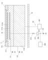
図3は、第1の例示的実施形態における基板支持部11及び電源30の構成例を示す。一実施形態において、基板支持部11は、静電チャック1111の内部に、チャック電極1111bと、基板バイアス電極1111cを有する。基板バイアス電極1111cは、チャック電極1111bの下方に配置され得る。基板バイアス電極1111cには、第1のパルス化DC信号を生成する第1のパルス化DC生成部200が電気的に接続されている。第1のパルス化DC生成部200は、上述の第1のDC生成部32aの一例であってよい。基台1110には、RF信号を生成するRF生成部201が電気的に接続されている。RF生成部201は、上述の第1のRF生成部31a及び/又は第2のRF生成部31bの一例であってよい。なお、一実施形態において、RF生成部201は、基板バイアス電極1111cに接続されていてよい。
First Exemplary Embodiment
3 shows an example of the configuration of the
一実施形態において、基板バイアス電極1111cと第1のパルス化DC生成部200との間には、第1のRFフィルタ210と第1のリンギング抑制回路211が接続されている。基板バイアス電極1111cは、接地されており、基板バイアス電極1111cと接地電位との間には、第1の寄生キャパシタC1が生じ得る。第1のパルス化DC生成部200から基板バイアス電極1111cまでの経路230は、接地されており、当該経路230上のノード231と接地電位との間には、第2の寄生キャパシタC2が生じ得る。さらに、基台1110は、接地されており、基台1110と接地電位との間には、第3の寄生キャパシタ3が生じ得る。
In one embodiment, a
一実施形態において、第1のRFフィルタ210は、RF生成部201から基台1110に供給されたRF信号が経路230を介して第1のパルス化DC生成部200に入り込むことを抑制するように構成されている。第1のRFフィルタ210は、RF信号の周波数に応じた特定の周波数の信号を除去し得る。第1のRFフィルタ210は、コイルであり得る。第1のRFフィルタ210は、チャンバ10の外部に配置され得る。
In one embodiment, the
第1のRFフィルタ210が有するコイルインダクタンスに起因して、第1の寄生キャパシタC1と第2の寄生キャパシタC2との間で共振が生じ、第1のパルス化DC生成部200から供給される第1のパルス化DC信号にリンギング(高周波成分)が生じ得る。一実施形態において、第1のリンギング抑制回路211は、第1のパルス化DC信号に重畳されるリンギングを抑制するように構成されている。第1のリンギング抑制回路211は、チャンバ10の外部に設けられ得る。第1のリンギング抑制回路211は、第1のRFフィルタ210と第1のパルス化DC生成部200との間に接続され得る。なお、第1のリンギング抑制回路211は、第1のRFフィルタ210と基板バイアス電極1111cとの間に接続され得る。
Due to the coil inductance of the
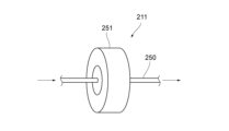
一実施形態において、図4に示すように、第1のリンギング抑制回路211は、経路230に接続される第1の導体250と、第1の導体250に配置された第1のフェライトコア251を含む。第1のフェライトコア251は、第1のパルスDC信号に重畳されるリンギングを除去し得る。
In one embodiment, as shown in FIG. 4, the first ringing
一実施形態において、第1のパルス化DC生成部200の第1のパルス化DC信号は、電圧パルスのシーケンスを有する。図5は、第1のパルス化DC生成部200で生成される第1の電圧パルスのシーケンスDC1の一例を示す。第1の電圧パルスのシーケンスDC1は、100kMzから1MHzの範囲内のパルス周波数を有する。第1の電圧パルスのシーケンスDC1は、繰り返しサイクルTを有する。第1の電圧パルスのシーケンスDC1は、各サイクルT内の第1の期間T1に第1の電圧レベルV1を有し、各サイクルTの第2の期間T2に、基準電圧レベルとなる第2の電圧レベルV2を有し得る。第1の電圧レベルV1の絶対値は、第2の電圧レベルV2の絶対値よりも大きい。一実施形態において、第1の電圧レベルV1は、負極性を有する。一実施形態において、第2の電圧レベルV2は、ゼロ電圧レベルを有する。一実施形態において、第1の電圧レベルV1は、0V~-15kVである。
In one embodiment, the first pulsed DC signal of the first pulsed
<プラズマ処理方法の一例>
プラズマ処理装置1を用いて行われるプラズマ処理は、プラズマを用いて基板W上の膜をエッチングするエッチング処理を含む。一実施形態において、プラズマ処理は、制御部2により実行される。
<An example of a plasma treatment method>
The plasma processing performed by using the
先ず、基板Wが、搬送アームによりチャンバ10内に搬入され、リフターにより基板支持部11に載置され、図2に示すように基板支持部11上に吸着保持される。
First, the substrate W is carried into the
次に、処理ガスが、ガス供給部20によりシャワーヘッド13に供給され、シャワーヘッド13からプラズマ処理空間10sに供給される。このとき供給される処理ガスは、基板Wのエッチング処理のために必要な活性種を生成するガスを含む。
Next, the processing gas is supplied to the
一実施形態において、下部電極及び/又は上部電極には、プラズマ生成用のソースRF信号が供給される。下部電極には、イオン引き込み用のバイアス信号が供給されてよい。このとき、プラズマ処理空間10s内の雰囲気はガス排出口10eから排気され、プラズマ処理空間10s内は所定の圧力に減圧されてもよい。これにより、プラズマ処理空間10sにプラズマが生成され、基板Wがエッチング処理される。
In one embodiment, a source RF signal for generating plasma is supplied to the lower electrode and/or the upper electrode. A bias signal for attracting ions may be supplied to the lower electrode. At this time, the atmosphere in the
プラズマ処理の一例において、図3に示す基台1110には、RF生成部201によりRF信号が供給される。基板バイアス電極1111cには、第1のパルス化DC生成部200により、バイアス信号として第1のパルス化DC信号が印加される。このとき、第1のRFフィルタ210により、RF生成部201から基台1110に供給されたRF信号が経路230を介して第1のパルス化DC生成部200に入り込むことが抑制される。また、第1のリンギング抑制回路211により、第1の寄生キャパシタC1と第2の寄生キャパシタC2との間に生じるリンギングが第1のパルス化DC信号に重畳されることが抑制される。
In one example of plasma processing, an RF signal is supplied to the
本例示的実施形態によれば、プラズマ処理装置1が、基台1110と、RF生成部201と、第1のパルス化DC生成部200と、第1のRFフィルタ210と、第1のリンギング抑制回路211とを含む。これにより、第1のパルス化DC生成部200から基板バイアス電極1111cに印加されるパルス化DC信号にリンギングが重畳することを抑制することができる。よって、パルス化DC信号を用いたプラズマ処理を適正に行うことができる。
According to this exemplary embodiment, the
(実施例)
パルス化DC生成部と基板バイアス電極との間に、リンギング抑制回路としてフェライトコアを配置した場合(フェライトコア有)とフェライトコアを配置しなかった場合(フェライトコア無)について、パルス化DC信号が印加された静電チャック上の基板電位を計測した。図6は、当該計測結果を示す。フェライトコアがある場合の基板電位は、フェライトコアがない場合に比べて、パルス化DC信号の矩形波形に近くなっており、パルス化DC信号に重畳するリンギング(高周波成分)が減少していることを確認することができる。また、フェライトコアがある場合の基板電位の絶対値が、フェライトコアがない場合に比べて高くなっている(図6中のΔV)ことを確認することができる。これにより、フェライトコアがある場合に、パルス化DC信号の電気エネルギが基板に効率的に伝達されていることを確認することができる。
(Example)
The substrate potential on the electrostatic chuck to which the pulsed DC signal was applied was measured for the case where a ferrite core was arranged as a ringing suppression circuit between the pulsed DC generating unit and the substrate bias electrode (with ferrite core) and the case where a ferrite core was not arranged (without ferrite core). FIG. 6 shows the measurement results. The substrate potential in the case where the ferrite core is present is closer to the rectangular waveform of the pulsed DC signal than in the case where the ferrite core is not present, and it can be confirmed that the ringing (high frequency component) superimposed on the pulsed DC signal is reduced. It can also be confirmed that the absolute value of the substrate potential in the case where the ferrite core is present is higher than that in the case where the ferrite core is not present (ΔV in FIG. 6). This makes it possible to confirm that the electric energy of the pulsed DC signal is efficiently transmitted to the substrate in the case where the ferrite core is present.
図7は、フェライトコアがない場合におけるプラズマ処理時の基板上のイオンエネルギ分布関数(IEDF(Ion Energy Distribution Function))を示す。図8は、フェライトコアがある場合におけるプラズマ処理時の基板上のイオンエネルギ分布関数を示す。フェライトコアがない場合は、イオンエネルギ(IE)が高い領域においてイオンエネルギ分布関数のピークが複数あるのに対し、フェライトコアがある場合は、イオンエネルギ(IE)が高い領域においてイオンエネルギ分布関数のピークが一つになっていることを確認することができる。これにより、フェライトコアがある場合に、基板上のイオンエネルギが高く安定することがわかる。 Figure 7 shows the ion energy distribution function (IEDF) on a substrate during plasma processing when there is no ferrite core. Figure 8 shows the ion energy distribution function on a substrate during plasma processing when there is a ferrite core. It can be seen that when there is no ferrite core, there are multiple peaks in the ion energy distribution function in the high ion energy (IE) region, whereas when there is a ferrite core, there is only one peak in the high ion energy (IE) region. This shows that when there is a ferrite core, the ion energy on the substrate is high and stable.
図9は、フェライトコアがある場合とフェライトコアがない場合について、エッチング処理における基板のエッチングレート(ER)を測定した結果である。図9の横軸は、パルス化DC信号のDC電圧である。フェライトコアがある場合のエッチングレートが、フェライトコアがない場合に比べて高くなることを確認することができる。 Figure 9 shows the results of measuring the etching rate (ER) of a substrate during etching processing with and without a ferrite core. The horizontal axis of Figure 9 is the DC voltage of the pulsed DC signal. It can be seen that the etching rate with a ferrite core is higher than that without a ferrite core.
上記実施の形態において、第1のリンギング抑制回路211は、図10に示すように、並列接続される複数の第1の導体250と、複数の第1の導体250の各々に配置される複数の第1のフェライトコア251を有していてよい。一実施形態において、各第1の導体250には、複数の第1のフェライトコア251が配置されていてよいし、一つの第1のフェライトコア251が配置されていてよい。かかる場合、パルス化DC信号により各第1の導体250に流れる電流が減少し、この結果、リンギングを除去することにより生じる第1のフェライトコア251の発熱を抑えることができる。
In the above embodiment, the first ringing
(第2の例示的実施形態)
図11は、第2の例示的実施形態における基板支持部11及び電源30の構成例を示す。一実施形態において、基板支持部11は、静電チャック1111の内部に、チャック電極1111bと、基板バイアス電極1111cに加えて、エッジリングバイアス電極1111dを有していてよい。エッジリングバイアス電極1111dは、エッジリング支持面の下方に配置され得る。エッジリングバイアス電極1111dには、第2のパルス化DC信号を生成する第2のパルス化DC生成部300が電気的に接続されている。
Second Exemplary Embodiment
11 shows an example of the configuration of the
一実施形態において、エッジリングバイアス電極1111dと第2のパルス化DC生成部300との間には、第2のRFフィルタ310と第2のリンギング抑制回路311が接続されている。エッジリングバイアス電極1111dは、接地されており、エッジリングバイアス電極1111dと接地電位との間には、第4の寄生キャパシタC4が生じ得る。第2のパルス化DC生成部300からエッジリングバイアス電極1111dまでの経路330は、接地されており、当該経路330上のノード331と接地電位との間には、第5の寄生キャパシタC5が生じ得る。
In one embodiment, a
一実施形態において、第2のRFフィルタ310は、RF生成部201から基台1110に供給されたRF信号が経路330を介して第2のパルス化DC生成部300に入り込むことを抑制するように構成されている。第2のRFフィルタ310は、RF信号の周波数に応じた特定の周波数の信号を除去し得る。第2のRFフィルタ310は、コイルであり得る。第2のRFフィルタ310は、チャンバ10の外部に設けられ得る。
In one embodiment, the
第2のRFフィルタ310が有するコイルインダクタンスに起因して、第4の寄生キャパシタC4と第5の寄生キャパシタC5との間で共振が生じ、第2のパルス化DC信号にリンギング(高周波成分)が生じ得る。一実施形態において、第2のリンギング抑制回路311は、第2のパルス化DC信号に重畳されるリンギングを抑制するように構成されている。第2のリンギング抑制回路311は、チャンバ10の外部に設けられ得る。第2のリンギング抑制回路311は、第2のRFフィルタ310と第2のパルス化DC生成部300との間に接続され得る。なお、第2のリンギング抑制回路311は、第2のRFフィルタ310とエッジリングバイアス電極1111dとの間に接続され得る。
Due to the coil inductance of the
一実施形態において、図12に示すように、第2のリンギング抑制回路311は、経路330に接続される第2の導体350と、第2の導体350に配置される第2のフェライトコア351を含む。各第2の導体350には、複数の第2のフェライトコア351が配置されていてよいし、一つの第2のフェライトコア351が配置されていてよい。第2のフェライトコア351は、第2のパルスDC信号に重畳されるリンギングを除去し得る。
In one embodiment, as shown in FIG. 12, the second ringing
第2のパルス化DC生成部300の第2のパルス化DC信号は、電圧パルスのシーケンスを有する。図13は、第2のパルス化DC生成部300で生成される第2の電圧パルスのシーケンスDC2の一例を示す。第2の電圧パルスのシーケンスDC2は、100kMzから1MHzの範囲内のパルス周波数を有する。一実施形態において、第2の電圧パルスのシーケンスDC2は、第1の電圧パルスのシーケンスDC1と同じ繰り返しサイクルTを有する。第2の電圧パルスのシーケンスDC2は、各サイクルT内の第1の期間T1に第3の電圧レベルV3を有し、各サイクルTの第2の期間T2に、基準電圧レベルとなる第4の電圧レベルV4を有し得る。第3の電圧レベルV3の絶対値は、第4の電圧レベルV4の絶対値よりも大きい。一実施形態において、第3の電圧レベルV3は、負極性を有する。一実施形態において、第4の電圧レベルV4は、ゼロ電圧レベルを有する。一実施形態において、第3の電圧レベルV3は、0V~-15kVである。
The second pulsed DC signal of the second pulsed
第2の例示的実施形態における基板支持部11及び電源30の他の構成は、第1の例示的実施形態と同様であってよい。
Other configurations of the
本例示的実施形態によれば、第2のパルス化DC生成部300からエッジリングバイアス電極1111dに印加されるパルス化DC信号にリンギングが重畳することを抑制することができる。よって、パルス化DC信号を用いたプラズマ処理を適正に行うことができる。
According to this exemplary embodiment, it is possible to suppress ringing from being superimposed on the pulsed DC signal applied from the second pulsed
以上の実施形態において、リンギング抑制回路は、フェライトコアに変えて、或いはフェライトコアと共に、ダンピング抵抗を有していてよい。 In the above embodiments, the ringing suppression circuit may have a damping resistor instead of or in addition to the ferrite core.
例えば、上記実施形態では、容量結合型のプラズマ装置を例に説明したが、これに限定されるものではなく、他のプラズマ装置に適用されてもよい。例えば、容量結合型のプラズマ装置に代えて、誘導結合型のプラズマ装置が用いられてもよい。この場合、誘導結合型のプラズマ装置は、アンテナ及び下部電極を含む。下部電極は、基板支持部内に配置され、アンテナは、チャンバの上部又は上方に配置される。一実施形態において、RF電源31は、アンテナに電気的に接続され、アンテナにRF信号を供給できてよい。
For example, in the above embodiment, a capacitively coupled plasma device has been described as an example, but the present invention is not limited to this and may be applied to other plasma devices. For example, an inductively coupled plasma device may be used instead of the capacitively coupled plasma device. In this case, the inductively coupled plasma device includes an antenna and a lower electrode. The lower electrode is disposed within the substrate support, and the antenna is disposed at or above the chamber. In one embodiment, the
本開示の実施形態は、以下の態様をさらに含む。 Embodiments of the present disclosure further include the following aspects:
(付記1)
プラズマ処理チャンバと、
前記プラズマ処理チャンバ内に配置される基板支持部であって、前記基板支持部は、導電性基台と、前記導電性基台上に配置される静電チャックと、前記静電チャック内に配置されるチャック電極と、前記静電チャック内において前記チャック電極の下方に配置されるバイアス電極と、を含む、前記基板支持部と、
前記基板支持部の上方に配置される上部電極と、
前記導電性基台、前記バイアス電極又は前記上部電極に電気的に接続され、RF信号を生成するように構成されるRF生成部と、
前記バイアス電極に電気的に接続され、パルス化DC信号を生成するように構成されるパルス化DC生成部と、
前記バイアス電極と前記パルス化DC生成部との間に接続されるRFフィルタと、
前記バイアス電極と前記パルス化DC生成部との間に接続され、前記パルス化DC信号に重畳されるリンギングを抑制するように構成されるリンギング抑制回路と、
を含む、プラズマ処理装置。
(Appendix 1)
a plasma processing chamber;
a substrate support disposed within the plasma processing chamber, the substrate support including: a conductive base; an electrostatic chuck disposed on the conductive base; a chucking electrode disposed within the electrostatic chuck; and a bias electrode disposed within the electrostatic chuck below the chucking electrode;
an upper electrode disposed above the substrate support;
an RF generating unit electrically connected to the conductive base, the bias electrode, or the upper electrode and configured to generate an RF signal;
a pulsed DC generator electrically connected to the bias electrode and configured to generate a pulsed DC signal;
an RF filter connected between the bias electrode and the pulsed DC generator;
A ringing suppression circuit is connected between the bias electrode and the pulsed DC generation unit and configured to suppress ringing superimposed on the pulsed DC signal.
A plasma processing apparatus comprising:
(付記2)
前記リンギング抑制回路は、少なくとも一つのフェライトコアを含む、付記1に記載のプラズマ処理装置。
(Appendix 2)
2. The plasma processing apparatus of
(付記3)
前記リンギング抑制回路は、
並列に接続される複数の導体と、
前記複数の導体の各々に少なくとも一つ配置される複数のフェライトコアと、を含む、付記1または2に記載のプラズマ処理装置。
(Appendix 3)
The ringing suppression circuit includes:
A plurality of conductors connected in parallel;
and a plurality of ferrite cores, at least one of which is disposed on each of the plurality of conductors.
(付記4)
前記パルス化DC信号は、電圧パルスのシーケンスを有する、付記1から3のいずれか一項に記載のプラズマ処理装置。
(Appendix 4)
4. The plasma processing apparatus of
(付記5)
前記電圧パルスのシーケンスは、負極性の電圧レベルを有する、付記4に記載のプラズマ処理装置。
(Appendix 5)
5. The plasma processing apparatus of claim 4, wherein the sequence of voltage pulses has negative voltage levels.
(付記6)
前記電圧パルスのシーケンスは、100kMzから1MHzの範囲内のパルス周波数を有する、付記4または5に記載のプラズマ処理装置。
(Appendix 6)
6. The plasma processing apparatus of claim 4 or 5, wherein the sequence of voltage pulses has a pulse frequency in the range of 100 kHz to 1 MHz.
(付記7)
前記パルス化DC信号は、各サイクル内の第1の期間に第1の電圧レベルを有し、各サイクル内の第2の期間に第2の電圧レベルを有する電圧パルスのシーケンスを有し、
前記第1の電圧レベルの絶対値が前記第2の電圧レベルの絶対値よりも大きい、付記1から3のいずれか一項に記載のプラズマ処理装置。
(Appendix 7)
the pulsed DC signal comprises a sequence of voltage pulses having a first voltage level for a first period in each cycle and a second voltage level for a second period in each cycle;
4. The plasma processing apparatus according to
(付記8)
前記第1の電圧レベルは、負極性を有する、付記7に記載のプラズマ処理装置。
(Appendix 8)
8. The plasma processing apparatus of claim 7, wherein the first voltage level has a negative polarity.
(付記9)
前記電圧パルスのシーケンスは、100kMzから1MHzの範囲内のパルス周波数を有する、付記7または8に記載のプラズマ処理装置。
(Appendix 9)
9. The plasma processing apparatus of claim 7 or 8, wherein the sequence of voltage pulses has a pulse frequency in the range of 100 kHz to 1 MHz.
(付記10)
前記第2の電圧レベルは、ゼロ電圧レベルを有する、付記7から9のいずれか一項に記載のプラズマ処理装置。
(Appendix 10)
10. The plasma processing apparatus of claim 7, wherein the second voltage level has a zero voltage level.
(付記11)
プラズマ処理チャンバと、
前記プラズマ処理チャンバ内に配置される基板支持部であって、前記基板支持部は、
基台と、
前記基台上に配置され、基板支持面及びエッジリング支持面を有する静電チャックと、
前記基板支持面上の基板を囲むように前記エッジリング支持面上に配置されるエッジリングと、
前記静電チャック内において前記基板支持面の下方に配置される基板バイアス電極と、
前記静電チャック内において前記エッジリング支持面の下方に配置されるエッジリングバイアス電極と、を含む、前記基板支持部と、
前記プラズマ処理チャンバ内にプラズマを生成するためのRF信号を生成するように構成されるRF生成部と、
前記基板バイアス電極に電気的に接続され、第1のパルス化DC信号を生成するように構成される第1のパルス化DC生成部と、
前記基板バイアス電極と前記第1のパルス化DC生成部との間に接続される第1のRFフィルタと、
前記基板バイアス電極と前記第1のパルス化DC生成部との間に接続され、前記第1のパルス化DC信号に重畳されるリンギングを抑制するように構成される第1のリンギング抑制回路と、
前記エッジリングバイアス電極に電気的に接続され、第2のパルス化DC信号を生成するように構成される第2のパルス化DC生成部と、
前記エッジリングバイアス電極と前記第2のパルス化DC生成部との間に接続される第2のRFフィルタと、
前記エッジリングバイアス電極と前記第2のパルス化DC生成部との間に接続され、前記第2のパルス化DC信号に重畳されるリンギングを抑制するように構成される第2のリンギング抑制回路と、
を含む、プラズマ処理装置。
(Appendix 11)
a plasma processing chamber;
A substrate support disposed within the plasma processing chamber, the substrate support comprising:
The base and
an electrostatic chuck disposed on the base and having a substrate support surface and an edge ring support surface;
an edge ring disposed on the edge ring support surface to surround a substrate on the substrate support surface;
a substrate bias electrode disposed within the electrostatic chuck below the substrate support surface;
an edge ring bias electrode disposed within the electrostatic chuck below the edge ring support surface;
an RF generator configured to generate an RF signal to generate a plasma in the plasma processing chamber;
a first pulsed DC generator electrically connected to the substrate bias electrode and configured to generate a first pulsed DC signal;
a first RF filter connected between the substrate bias electrode and the first pulsed DC generator;
a first ringing suppression circuit connected between the substrate bias electrode and the first pulsed DC generation unit and configured to suppress ringing superimposed on the first pulsed DC signal;
a second pulsed DC generator electrically connected to the edge ring bias electrode and configured to generate a second pulsed DC signal;
a second RF filter connected between the edge ring bias electrode and the second pulsed DC generator;
a second ringing suppression circuit connected between the edge ring bias electrode and the second pulsed DC generator and configured to suppress ringing superimposed on the second pulsed DC signal;
A plasma processing apparatus comprising:
(付記12)
前記第1のリンギング抑制回路は、少なくとも一つの第1のフェライトコアを含む、付記11に記載のプラズマ処理装置。
(Appendix 12)
12. The plasma processing apparatus of
(付記13)
前記第2のリンギング抑制回路は、少なくとも一つの第2のフェライトコアを含む、付記11または12に記載のプラズマ処理装置。
(Appendix 13)
13. The plasma processing apparatus according to
(付記14)
前記第2のリンギング抑制回路は、
並列に接続される複数の第2の導体と、
前記複数の第2の導体の各々に少なくとも一つ配置される複数の第2のフェライトコアと、を含む、付記11に記載のプラズマ処理装置。
(Appendix 14)
The second ringing suppression circuit includes:
a plurality of second conductors connected in parallel;
and a plurality of second ferrite cores, at least one of which is disposed on each of the plurality of second conductors.
(付記15)
前記第1のリンギング抑制回路は、
並列に接続される複数の第1の導体と、
前記複数の第1の導体の各々に少なくとも一つ配置される複数の第1のフェライトコアと、を含む、付記11に記載のプラズマ処理装置。
(Appendix 15)
The first ringing suppression circuit includes:
a plurality of first conductors connected in parallel;
and a plurality of first ferrite cores, at least one of which is disposed on each of the plurality of first conductors.
(付記16)
前記第2のリンギング抑制回路は、少なくとも一つの第2のフェライトコアを含む、付記15に記載のプラズマ処理装置。
(Appendix 16)
16. The plasma processing apparatus of claim 15, wherein the second ringing suppression circuit includes at least one second ferrite core.
(付記17)
前記第2のリンギング抑制回路は、
並列に接続される複数の第2の導体と、
前記複数の第2の導体の各々に少なくとも一つ配置される複数の第2のフェライトコアと、を含む、付記15または16に記載のプラズマ処理装置。
(Appendix 17)
The second ringing suppression circuit includes:
a plurality of second conductors connected in parallel;
and a plurality of second ferrite cores, at least one of which is arranged on each of the plurality of second conductors.
(付記18)
プラズマ処理チャンバと、
前記プラズマ処理チャンバ内に配置される基板支持部であって、前記基板支持部は、基台と、前記基台上に配置される静電チャックと、前記静電チャック内に配置されるバイアス電極と、を含む、前記基板支持部と、
前記プラズマ処理チャンバ内にプラズマを生成するためのRF信号を生成するように構成されるRF生成部と、
前記バイアス電極に電気的に接続され、パルス化DC信号を生成するように構成されるパルス化DC生成部と、
前記バイアス電極と前記パルス化DC生成部との間に接続され、第1の寄生キャパシタと第2の寄生キャパシタとの間に生じるリンギングが前記パルス化DC信号に重畳されることを抑制するように構成されるリンギング抑制回路であって、前記第1の寄生キャパシタは、前記バイアス電極と接地電位との間に生じ、前記第2の寄生キャパシタは、前記パルス化DC生成部から前記バイアス電極までの経路上のノードと接地電位との間に生じる、前記リンギング抑制回路と、
を含む、プラズマ処理装置。
(Appendix 18)
a plasma processing chamber;
a substrate support disposed within the plasma processing chamber, the substrate support including a base, an electrostatic chuck disposed on the base, and a bias electrode disposed within the electrostatic chuck;
an RF generator configured to generate an RF signal to generate a plasma in the plasma processing chamber;
a pulsed DC generator electrically connected to the bias electrode and configured to generate a pulsed DC signal;
A ringing suppression circuit is connected between the bias electrode and the pulsed DC generation unit, and is configured to suppress ringing occurring between a first parasitic capacitor and a second parasitic capacitor from being superimposed on the pulsed DC signal, the first parasitic capacitor occurring between the bias electrode and a ground potential, and the second parasitic capacitor occurring between a node on a path from the pulsed DC generation unit to the bias electrode and a ground potential;
A plasma processing apparatus comprising:
(付記19)
前記リンギング抑制回路は、少なくとも一つのフェライトコアを含む、付記18に記載のプラズマ処理装置。
(Appendix 19)
20. The plasma processing apparatus of claim 18, wherein the ringing suppression circuit includes at least one ferrite core.
(付記20)
前記リンギング抑制回路は、
並列に接続される複数の導体と、
前記複数の導体の各々に少なくとも一つ配置される複数のフェライトコアと、を含む、付記18または19に記載のプラズマ処理装置。
(Appendix 20)
The ringing suppression circuit includes:
A plurality of conductors connected in parallel;
20. The plasma processing apparatus of claim 18 or 19, further comprising: a plurality of ferrite cores, at least one of which is disposed on each of the plurality of conductors.
以上の各実施形態は、説明の目的で記載されており、本開示の範囲を限定することを意図するものではない。以上の各実施形態は、本開示の範囲及び趣旨から逸脱することなく種々の変形をなし得る。例えば、ある実施形態における一部の構成要素を、他の実施形態に追加することができる。また、ある実施形態における一部の構成要素を、他の実施形態の対応する構成要素と置換することができる。 The above embodiments are described for the purpose of explanation and are not intended to limit the scope of the present disclosure. Various modifications of the above embodiments may be made without departing from the scope and spirit of the present disclosure. For example, some components in one embodiment may be added to another embodiment. Also, some components in one embodiment may be replaced with corresponding components in another embodiment.
1……プラズマ処理装置、10……チャンバ、11……基板支持部、30……電源、1110……基台、1111……静電チャック、1111c……基板バイアス電極、200……第1のパルス化DC生成部、201……RF生成部、210……第1のRFフィルタ、211……第1のリンギング抑制回路、W…基板
REFERENCE SIGNS LIST 1: plasma processing apparatus, 10: chamber, 11: substrate support, 30: power supply, 1110: base, 1111: electrostatic chuck, 1111c: substrate bias electrode, 200: first pulsed DC generating unit, 201: RF generating unit, 210: first RF filter, 211: first ringing suppression circuit, W: substrate
Claims (20)
前記プラズマ処理チャンバ内に配置される基板支持部であって、前記基板支持部は、導電性基台と、前記導電性基台上に配置される静電チャックと、前記静電チャック内に配置されるチャック電極と、前記静電チャック内において前記チャック電極の下方に配置されるバイアス電極と、を含む、前記基板支持部と、
前記基板支持部の上方に配置される上部電極と、
前記導電性基台、前記バイアス電極又は前記上部電極に電気的に接続され、RF信号を生成するように構成されるRF生成部と、
前記バイアス電極に電気的に接続され、パルス化DC信号を生成するように構成されるパルス化DC生成部と、
前記バイアス電極と前記パルス化DC生成部との間に接続されるRFフィルタと、
前記バイアス電極と前記パルス化DC生成部との間に接続され、前記パルス化DC信号に重畳されるリンギングを抑制するように構成されるリンギング抑制回路と、
を含む、プラズマ処理装置。 a plasma processing chamber;
a substrate support disposed within the plasma processing chamber, the substrate support including: a conductive base; an electrostatic chuck disposed on the conductive base; a chucking electrode disposed within the electrostatic chuck; and a bias electrode disposed within the electrostatic chuck below the chucking electrode;
an upper electrode disposed above the substrate support;
an RF generating unit electrically connected to the conductive base, the bias electrode, or the upper electrode and configured to generate an RF signal;
a pulsed DC generator electrically connected to the bias electrode and configured to generate a pulsed DC signal;
an RF filter connected between the bias electrode and the pulsed DC generator;
A ringing suppression circuit is connected between the bias electrode and the pulsed DC generation unit and configured to suppress ringing superimposed on the pulsed DC signal.
A plasma processing apparatus comprising:
並列に接続される複数の導体と、
前記複数の導体の各々に少なくとも一つ配置される複数のフェライトコアと、を含む、請求項1に記載のプラズマ処理装置。 The ringing suppression circuit includes:
A plurality of conductors connected in parallel;
The plasma processing apparatus according to claim 1 , further comprising: a plurality of ferrite cores, at least one of which is disposed on each of the plurality of conductors.
前記第1の電圧レベルの絶対値が前記第2の電圧レベルの絶対値よりも大きい、請求項1から3のいずれか一項に記載のプラズマ処理装置。 the pulsed DC signal comprises a sequence of voltage pulses having a first voltage level for a first period in each cycle and a second voltage level for a second period in each cycle;
The plasma processing apparatus according to claim 1 , wherein an absolute value of the first voltage level is greater than an absolute value of the second voltage level.
前記プラズマ処理チャンバ内に配置される基板支持部であって、前記基板支持部は、
基台と、
前記基台上に配置され、基板支持面及びエッジリング支持面を有する静電チャックと、
前記基板支持面上の基板を囲むように前記エッジリング支持面上に配置されるエッジリングと、
前記静電チャック内において前記基板支持面の下方に配置される基板バイアス電極と、
前記静電チャック内において前記エッジリング支持面の下方に配置されるエッジリングバイアス電極と、を含む、前記基板支持部と、
前記プラズマ処理チャンバ内にプラズマを生成するためのRF信号を生成するように構成されるRF生成部と、
前記基板バイアス電極に電気的に接続され、第1のパルス化DC信号を生成するように構成される第1のパルス化DC生成部と、
前記基板バイアス電極と前記第1のパルス化DC生成部との間に接続される第1のRFフィルタと、
前記基板バイアス電極と前記第1のパルス化DC生成部との間に接続され、前記第1のパルス化DC信号に重畳されるリンギングを抑制するように構成される第1のリンギング抑制回路と、
前記エッジリングバイアス電極に電気的に接続され、第2のパルス化DC信号を生成するように構成される第2のパルス化DC生成部と、
前記エッジリングバイアス電極と前記第2のパルス化DC生成部との間に接続される第2のRFフィルタと、
前記エッジリングバイアス電極と前記第2のパルス化DC生成部との間に接続され、前記第2のパルス化DC信号に重畳されるリンギングを抑制するように構成される第2のリンギング抑制回路と、
を含む、プラズマ処理装置。 a plasma processing chamber;
A substrate support disposed within the plasma processing chamber, the substrate support comprising:
The base and
an electrostatic chuck disposed on the base and having a substrate support surface and an edge ring support surface;
an edge ring disposed on the edge ring support surface to surround a substrate on the substrate support surface;
a substrate bias electrode disposed within the electrostatic chuck below the substrate support surface;
an edge ring bias electrode disposed within the electrostatic chuck below the edge ring support surface;
an RF generator configured to generate an RF signal to generate a plasma in the plasma processing chamber;
a first pulsed DC generator electrically connected to the substrate bias electrode and configured to generate a first pulsed DC signal;
a first RF filter connected between the substrate bias electrode and the first pulsed DC generator;
a first ringing suppression circuit connected between the substrate bias electrode and the first pulsed DC generation unit and configured to suppress ringing superimposed on the first pulsed DC signal;
a second pulsed DC generator electrically connected to the edge ring bias electrode and configured to generate a second pulsed DC signal;
a second RF filter connected between the edge ring bias electrode and the second pulsed DC generator;
a second ringing suppression circuit connected between the edge ring bias electrode and the second pulsed DC generator and configured to suppress ringing superimposed on the second pulsed DC signal;
A plasma processing apparatus comprising:
並列に接続される複数の第2の導体と、
前記複数の第2の導体の各々に少なくとも一つ配置される複数の第2のフェライトコアと、を含む、請求項11に記載のプラズマ処理装置。 The second ringing suppression circuit includes:
a plurality of second conductors connected in parallel;
The plasma processing apparatus according to claim 11 , further comprising: a plurality of second ferrite cores, at least one of which is disposed in each of the plurality of second conductors.
並列に接続される複数の第1の導体と、
前記複数の第1の導体の各々に少なくとも一つ配置される複数の第1のフェライトコアと、を含む、請求項11に記載のプラズマ処理装置。 The first ringing suppression circuit includes:
a plurality of first conductors connected in parallel;
The plasma processing apparatus of claim 11 , further comprising: a plurality of first ferrite cores, at least one of which is disposed in each of the plurality of first conductors.
並列に接続される複数の第2の導体と、
前記複数の第2の導体の各々に少なくとも一つ配置される複数の第2のフェライトコアと、を含む、請求項15に記載のプラズマ処理装置。 The second ringing suppression circuit includes:
a plurality of second conductors connected in parallel;
The plasma processing apparatus of claim 15 , further comprising: a plurality of second ferrite cores, at least one of which is disposed in each of the plurality of second conductors.
前記プラズマ処理チャンバ内に配置される基板支持部であって、前記基板支持部は、基台と、前記基台上に配置される静電チャックと、前記静電チャック内に配置されるバイアス電極と、を含む、前記基板支持部と、
前記プラズマ処理チャンバ内にプラズマを生成するためのRF信号を生成するように構成されるRF生成部と、
前記バイアス電極に電気的に接続され、パルス化DC信号を生成するように構成されるパルス化DC生成部と、
前記バイアス電極と前記パルス化DC生成部との間に接続され、第1の寄生キャパシタと第2の寄生キャパシタとの間に生じるリンギングが前記パルス化DC信号に重畳されることを抑制するように構成されるリンギング抑制回路であって、前記第1の寄生キャパシタは、前記バイアス電極と接地電位との間に生じ、前記第2の寄生キャパシタは、前記パルス化DC生成部から前記バイアス電極までの経路上のノードと接地電位との間に生じる、前記リンギング抑制回路と、
を含む、プラズマ処理装置。 a plasma processing chamber;
a substrate support disposed within the plasma processing chamber, the substrate support including a base, an electrostatic chuck disposed on the base, and a bias electrode disposed within the electrostatic chuck;
an RF generator configured to generate an RF signal to generate a plasma in the plasma processing chamber;
a pulsed DC generator electrically connected to the bias electrode and configured to generate a pulsed DC signal;
A ringing suppression circuit is connected between the bias electrode and the pulsed DC generation unit, and is configured to suppress ringing occurring between a first parasitic capacitor and a second parasitic capacitor from being superimposed on the pulsed DC signal, the first parasitic capacitor occurring between the bias electrode and a ground potential, and the second parasitic capacitor occurring between a node on a path from the pulsed DC generation unit to the bias electrode and a ground potential;
A plasma processing apparatus comprising:
並列に接続される複数の導体と、
前記複数の導体の各々に少なくとも一つ配置される複数のフェライトコアと、を含む、請求項18に記載のプラズマ処理装置。
The ringing suppression circuit includes:
A plurality of conductors connected in parallel;
The plasma processing apparatus of claim 18 , further comprising: a plurality of ferrite cores, at least one of which is disposed on each of the plurality of conductors.
Priority Applications (5)
| Application Number | Priority Date | Filing Date | Title |
|---|---|---|---|
| JP2025500738A JP7763025B2 (en) | 2023-02-14 | 2024-01-19 | Plasma processing equipment |
| CN202480010654.4A CN120642580A (en) | 2023-02-14 | 2024-01-19 | Plasma processing apparatus |
| KR1020257029089A KR20250135905A (en) | 2023-02-14 | 2024-01-19 | plasma treatment device |
| US19/291,683 US20250357088A1 (en) | 2023-02-14 | 2025-08-06 | Plasma processing apparatus |
| JP2025175083A JP2026012789A (en) | 2023-02-14 | 2025-10-17 | Plasma processing equipment |
Applications Claiming Priority (2)
| Application Number | Priority Date | Filing Date | Title |
|---|---|---|---|
| JP2023020807 | 2023-02-14 | ||
| JP2023-020807 | 2023-02-14 |
Related Child Applications (1)
| Application Number | Title | Priority Date | Filing Date |
|---|---|---|---|
| US19/291,683 Continuation US20250357088A1 (en) | 2023-02-14 | 2025-08-06 | Plasma processing apparatus |
Publications (1)
| Publication Number | Publication Date |
|---|---|
| WO2024171715A1 true WO2024171715A1 (en) | 2024-08-22 |
Family
ID=92421435
Family Applications (1)
| Application Number | Title | Priority Date | Filing Date |
|---|---|---|---|
| PCT/JP2024/001422 Ceased WO2024171715A1 (en) | 2023-02-14 | 2024-01-19 | Plasma processing device |
Country Status (6)
| Country | Link |
|---|---|
| US (1) | US20250357088A1 (en) |
| JP (2) | JP7763025B2 (en) |
| KR (1) | KR20250135905A (en) |
| CN (1) | CN120642580A (en) |
| TW (1) | TW202507791A (en) |
| WO (1) | WO2024171715A1 (en) |
Cited By (1)
| Publication number | Priority date | Publication date | Assignee | Title |
|---|---|---|---|---|
| CN119170554A (en) * | 2024-11-19 | 2024-12-20 | 中微半导体设备(上海)股份有限公司 | Bottom electrode assembly and plasma processing apparatus |
Citations (4)
| Publication number | Priority date | Publication date | Assignee | Title |
|---|---|---|---|---|
| JPH0993803A (en) * | 1995-09-25 | 1997-04-04 | Fujitsu Ltd | Power supply surge suppression circuit |
| JP2002184770A (en) * | 2000-12-19 | 2002-06-28 | Shimadzu Corp | Substrate processing equipment |
| JP2016072001A (en) * | 2014-09-29 | 2016-05-09 | 株式会社ダイヘン | High frequency power supply |
| WO2022202702A1 (en) * | 2021-03-24 | 2022-09-29 | 東京エレクトロン株式会社 | Plasma processing apparatus and filter unit |
Family Cites Families (10)
| Publication number | Priority date | Publication date | Assignee | Title |
|---|---|---|---|---|
| JP3663392B2 (en) * | 1996-03-01 | 2005-06-22 | 株式会社日立製作所 | Plasma etching processing equipment |
| JP5864879B2 (en) * | 2011-03-31 | 2016-02-17 | 東京エレクトロン株式会社 | Substrate processing apparatus and control method thereof |
| CN203942472U (en) * | 2014-07-17 | 2014-11-12 | 中国船舶重工集团公司第七一七研究所 | A kind of pwm pulse harmonic wave that improves Electro Magnetic Compatibility suppresses system |
| JP6869034B2 (en) * | 2017-01-17 | 2021-05-12 | 東京エレクトロン株式会社 | Plasma processing equipment |
| WO2021241201A1 (en) * | 2020-05-29 | 2021-12-02 | 東京エレクトロン株式会社 | Power supply system, and plasma processing device |
| CN111711354B (en) * | 2020-07-07 | 2025-03-11 | 金波 | DC system anti-rebound interference power filter |
| US11848176B2 (en) | 2020-07-31 | 2023-12-19 | Applied Materials, Inc. | Plasma processing using pulsed-voltage and radio-frequency power |
| US11948780B2 (en) * | 2021-05-12 | 2024-04-02 | Applied Materials, Inc. | Automatic electrostatic chuck bias compensation during plasma processing |
| JP7668157B2 (en) * | 2021-05-19 | 2025-04-24 | 東京エレクトロン株式会社 | SUBSTRATE SUPPORT, PLASMA PROCESSING APPARATUS, AND PLASMA PROCESSING METHOD |
| CN115692190A (en) * | 2021-07-28 | 2023-02-03 | 东京毅力科创株式会社 | Plasma processing method, plasma processing device and system |
-
2024
- 2024-01-19 WO PCT/JP2024/001422 patent/WO2024171715A1/en not_active Ceased
- 2024-01-19 JP JP2025500738A patent/JP7763025B2/en active Active
- 2024-01-19 KR KR1020257029089A patent/KR20250135905A/en active Pending
- 2024-01-19 CN CN202480010654.4A patent/CN120642580A/en active Pending
- 2024-01-31 TW TW113103683A patent/TW202507791A/en unknown
-
2025
- 2025-08-06 US US19/291,683 patent/US20250357088A1/en active Pending
- 2025-10-17 JP JP2025175083A patent/JP2026012789A/en active Pending
Patent Citations (4)
| Publication number | Priority date | Publication date | Assignee | Title |
|---|---|---|---|---|
| JPH0993803A (en) * | 1995-09-25 | 1997-04-04 | Fujitsu Ltd | Power supply surge suppression circuit |
| JP2002184770A (en) * | 2000-12-19 | 2002-06-28 | Shimadzu Corp | Substrate processing equipment |
| JP2016072001A (en) * | 2014-09-29 | 2016-05-09 | 株式会社ダイヘン | High frequency power supply |
| WO2022202702A1 (en) * | 2021-03-24 | 2022-09-29 | 東京エレクトロン株式会社 | Plasma processing apparatus and filter unit |
Cited By (2)
| Publication number | Priority date | Publication date | Assignee | Title |
|---|---|---|---|---|
| CN119170554A (en) * | 2024-11-19 | 2024-12-20 | 中微半导体设备(上海)股份有限公司 | Bottom electrode assembly and plasma processing apparatus |
| CN119170554B (en) * | 2024-11-19 | 2025-07-08 | 中微半导体设备(上海)股份有限公司 | Bottom electrode assembly and plasma processing apparatus |
Also Published As
| Publication number | Publication date |
|---|---|
| KR20250135905A (en) | 2025-09-15 |
| US20250357088A1 (en) | 2025-11-20 |
| TW202507791A (en) | 2025-02-16 |
| CN120642580A (en) | 2025-09-12 |
| JPWO2024171715A1 (en) | 2024-08-22 |
| JP2026012789A (en) | 2026-01-27 |
| JP7763025B2 (en) | 2025-10-31 |
Similar Documents
| Publication | Publication Date | Title |
|---|---|---|
| JP2026012789A (en) | Plasma processing equipment | |
| JP2025172109A (en) | Plasma processing method and plasma processing apparatus | |
| WO2024171714A1 (en) | Plasma treatment device | |
| US20260088250A1 (en) | Plasma processing apparatus | |
| WO2025053086A1 (en) | Plasma processing device and plasma processing method | |
| WO2024257401A1 (en) | Plasma processing device | |
| JP2024094874A (en) | Plasma Processing Equipment | |
| US20250226181A1 (en) | Plasma processing apparatus and power supply system | |
| JP2025029851A (en) | Plasma Processing Equipment | |
| WO2024070580A1 (en) | Plasma processing device and power supply system | |
| WO2026034233A1 (en) | Plasma treatment device and power source system | |
| WO2026004597A1 (en) | Plasma processing apparatus | |
| WO2025253941A1 (en) | Plasma processing device | |
| WO2025134798A1 (en) | Plasma processing device and cleaning method | |
| WO2026034234A1 (en) | Plasma processing device and power supply system | |
| WO2025169734A1 (en) | Plasma processing device | |
| WO2025089081A1 (en) | Plasma processing device | |
| JP2025173686A (en) | Plasma processing equipment | |
| JP2025064037A (en) | Electrostatic chuck, substrate support, and plasma processing apparatus | |
| JP2025127899A (en) | Plasma processing equipment | |
| WO2024018960A1 (en) | Plasma processing device and plasma processing method | |
| JP2026013822A (en) | Plasma processing apparatus and electrostatic chuck | |
| JP2025090149A (en) | Plasma processing method and plasma processing apparatus | |
| WO2026088796A1 (en) | Plasma processing device and power supply system | |
| WO2025169740A1 (en) | Plasma processing device, power supply system, control method, and program |
Legal Events
| Date | Code | Title | Description |
|---|---|---|---|
| 121 | Ep: the epo has been informed by wipo that ep was designated in this application |
Ref document number: 24756566 Country of ref document: EP Kind code of ref document: A1 |
|
| ENP | Entry into the national phase |
Ref document number: 2025500738 Country of ref document: JP Kind code of ref document: A |
|
| WWE | Wipo information: entry into national phase |
Ref document number: 2025500738 Country of ref document: JP |
|
| WWE | Wipo information: entry into national phase |
Ref document number: 202480010654.4 Country of ref document: CN |
|
| WWP | Wipo information: published in national office |
Ref document number: 202480010654.4 Country of ref document: CN |
|
| NENP | Non-entry into the national phase |
Ref country code: DE |
|
| WWE | Wipo information: entry into national phase |
Ref document number: 11202505279V Country of ref document: SG |
|
| WWP | Wipo information: published in national office |
Ref document number: 11202505279V Country of ref document: SG |
|
| 122 | Ep: pct application non-entry in european phase |
Ref document number: 24756566 Country of ref document: EP Kind code of ref document: A1 |