WO2022067581A1 - 显示面板及显示装置 - Google Patents
显示面板及显示装置 Download PDFInfo
- Publication number
- WO2022067581A1 WO2022067581A1 PCT/CN2020/119087 CN2020119087W WO2022067581A1 WO 2022067581 A1 WO2022067581 A1 WO 2022067581A1 CN 2020119087 W CN2020119087 W CN 2020119087W WO 2022067581 A1 WO2022067581 A1 WO 2022067581A1
- Authority
- WO
- WIPO (PCT)
- Prior art keywords
- pixel
- sub
- base substrate
- orthographic projection
- color sub
- Prior art date
- Legal status (The legal status is an assumption and is not a legal conclusion. Google has not performed a legal analysis and makes no representation as to the accuracy of the status listed.)
- Ceased
Links
Images




Classifications
-
- H—ELECTRICITY
- H10—SEMICONDUCTOR DEVICES; ELECTRIC SOLID-STATE DEVICES NOT OTHERWISE PROVIDED FOR
- H10K—ORGANIC ELECTRIC SOLID-STATE DEVICES
- H10K59/00—Integrated devices, or assemblies of multiple devices, comprising at least one organic light-emitting element covered by group H10K50/00
- H10K59/30—Devices specially adapted for multicolour light emission
- H10K59/35—Devices specially adapted for multicolour light emission comprising red-green-blue [RGB] subpixels
- H10K59/353—Devices specially adapted for multicolour light emission comprising red-green-blue [RGB] subpixels characterised by the geometrical arrangement of the RGB subpixels
-
- H—ELECTRICITY
- H10—SEMICONDUCTOR DEVICES; ELECTRIC SOLID-STATE DEVICES NOT OTHERWISE PROVIDED FOR
- H10K—ORGANIC ELECTRIC SOLID-STATE DEVICES
- H10K59/00—Integrated devices, or assemblies of multiple devices, comprising at least one organic light-emitting element covered by group H10K50/00
- H10K59/10—OLED displays
- H10K59/12—Active-matrix OLED [AMOLED] displays
- H10K59/121—Active-matrix OLED [AMOLED] displays characterised by the geometry or disposition of pixel elements
-
- H—ELECTRICITY
- H10—SEMICONDUCTOR DEVICES; ELECTRIC SOLID-STATE DEVICES NOT OTHERWISE PROVIDED FOR
- H10K—ORGANIC ELECTRIC SOLID-STATE DEVICES
- H10K59/00—Integrated devices, or assemblies of multiple devices, comprising at least one organic light-emitting element covered by group H10K50/00
- H10K59/10—OLED displays
- H10K59/12—Active-matrix OLED [AMOLED] displays
- H10K59/122—Pixel-defining structures or layers, e.g. banks
-
- H—ELECTRICITY
- H10—SEMICONDUCTOR DEVICES; ELECTRIC SOLID-STATE DEVICES NOT OTHERWISE PROVIDED FOR
- H10K—ORGANIC ELECTRIC SOLID-STATE DEVICES
- H10K59/00—Integrated devices, or assemblies of multiple devices, comprising at least one organic light-emitting element covered by group H10K50/00
- H10K59/10—OLED displays
- H10K59/12—Active-matrix OLED [AMOLED] displays
- H10K59/124—Insulating layers formed between TFT elements and OLED elements
-
- H—ELECTRICITY
- H10—SEMICONDUCTOR DEVICES; ELECTRIC SOLID-STATE DEVICES NOT OTHERWISE PROVIDED FOR
- H10K—ORGANIC ELECTRIC SOLID-STATE DEVICES
- H10K59/00—Integrated devices, or assemblies of multiple devices, comprising at least one organic light-emitting element covered by group H10K50/00
- H10K59/30—Devices specially adapted for multicolour light emission
- H10K59/35—Devices specially adapted for multicolour light emission comprising red-green-blue [RGB] subpixels
- H10K59/352—Devices specially adapted for multicolour light emission comprising red-green-blue [RGB] subpixels the areas of the RGB subpixels being different
-
- G—PHYSICS
- G09—EDUCATION; CRYPTOGRAPHY; DISPLAY; ADVERTISING; SEALS
- G09G—ARRANGEMENTS OR CIRCUITS FOR CONTROL OF INDICATING DEVICES USING STATIC MEANS TO PRESENT VARIABLE INFORMATION
- G09G2300/00—Aspects of the constitution of display devices
- G09G2300/04—Structural and physical details of display devices
- G09G2300/0421—Structural details of the set of electrodes
- G09G2300/0426—Layout of electrodes and connections
-
- G—PHYSICS
- G09—EDUCATION; CRYPTOGRAPHY; DISPLAY; ADVERTISING; SEALS
- G09G—ARRANGEMENTS OR CIRCUITS FOR CONTROL OF INDICATING DEVICES USING STATIC MEANS TO PRESENT VARIABLE INFORMATION
- G09G3/00—Control arrangements or circuits, of interest only in connection with visual indicators other than cathode-ray tubes
- G09G3/20—Control arrangements or circuits, of interest only in connection with visual indicators other than cathode-ray tubes for presentation of an assembly of a number of characters, e.g. a page, by composing the assembly by combination of individual elements arranged in a matrix no fixed position being assigned to or needed to be assigned to the individual characters or partial characters
- G09G3/22—Control arrangements or circuits, of interest only in connection with visual indicators other than cathode-ray tubes for presentation of an assembly of a number of characters, e.g. a page, by composing the assembly by combination of individual elements arranged in a matrix no fixed position being assigned to or needed to be assigned to the individual characters or partial characters using controlled light sources
- G09G3/30—Control arrangements or circuits, of interest only in connection with visual indicators other than cathode-ray tubes for presentation of an assembly of a number of characters, e.g. a page, by composing the assembly by combination of individual elements arranged in a matrix no fixed position being assigned to or needed to be assigned to the individual characters or partial characters using controlled light sources using electroluminescent panels
-
- H—ELECTRICITY
- H10—SEMICONDUCTOR DEVICES; ELECTRIC SOLID-STATE DEVICES NOT OTHERWISE PROVIDED FOR
- H10K—ORGANIC ELECTRIC SOLID-STATE DEVICES
- H10K59/00—Integrated devices, or assemblies of multiple devices, comprising at least one organic light-emitting element covered by group H10K50/00
- H10K59/10—OLED displays
- H10K59/12—Active-matrix OLED [AMOLED] displays
- H10K59/131—Interconnections, e.g. wiring lines or terminals
Definitions
- the embodiments of the present disclosure relate to the field of display technology, and in particular, to a display panel and a display device.
- OLED Organic Light Emitting Diode
- a base substrate including a plurality of sub-pixels:
- transistor array layer located on the base substrate, and the transistor array layer includes an anode transfer part located in each of the sub-pixels;
- a first flat layer located on the side of the transistor array layer away from the base substrate;
- a first electrode layer located on the side of the first flat layer away from the base substrate, the first electrode layer includes an anode located in each of the sub-pixels; wherein the anode includes a main body part that is electrically connected to each other and the via hole portion; and the via hole portion in each of the sub-pixels is electrically connected to the anode transfer portion through a first via hole; the first via hole penetrates the first flat layer;
- the plurality of sub-pixels include first-color sub-pixels and second-color sub-pixels adjacent to each other along the first direction; the first via hole in the first-color sub-pixel is located at the orthographic projection of the base substrate The main body portion in the first color sub-pixel and the main body portion in the second color sub-pixel are between the orthographic projections of the base substrate;
- one side of the anode in the second color sub-pixel faces the first color sub-pixel in the orthographic projection of the base substrate
- the anode in the pixel has a first recess on the orthographic projection side of the base substrate; and the first recess is disposed toward the center of the main body of the second color sub-pixel;
- the display panel includes a plurality of repeating units, and each repeating unit includes at least one sub-pixel of the first color and at least one sub-pixel of the second color;
- Two adjacent repeating units have at least two of the first recesses and two of the first via holes; and, in the first direction, at least two adjacent repeating units have The two first recesses and the first via holes are arranged on the same straight line.
- the orthographic projection of the first recess of the anode in the second color sub-pixel in the second direction covers where the first via hole in the first color sub-pixel is located. orthographic projection in the second direction.
- the orthographic projection of the via portion on the base substrate covers the orthographic projection of the first via on the base substrate
- the first recess is disposed in the main body portion of the second color sub-pixel, and the orthographic projection of the first recess in the second direction covers the via portion in the first color sub-pixel in the first color sub-pixel. Orthographic projection in two directions.
- an edge of the orthographic projection of the first recess on the base substrate is substantially parallel to an edge of the orthographic projection of the base substrate of the via portion in the first color sub-pixel.
- the first recess is between an edge of the orthographic projection of the base substrate and an edge of the orthographic projection of the base substrate of the via portion in the first color sub-pixel The distance is 2.5 to 20 ⁇ m.
- the first color sub-pixel is a red sub-pixel
- the second color sub-pixel is a green sub-pixel
- the transistor array layer includes a driving transistor located in each of the sub-pixels; the orthographic projection of the anode in the green sub-pixel on the base substrate and the channel region of the driving transistor in the red sub-pixel are located there.
- the orthographic projection of the base substrate has an overlapping area.
- the orthographic projection of the anode in the red sub-pixel on the base substrate does not overlap with the orthographic projection of the channel region of each of the driving transistors on the base substrate.
- the transistor array layer includes: a plurality of scan lines, a plurality of reset lines, and a plurality of light-emitting control lines spaced apart from each other; wherein, one of the repeating units corresponds to at least one of the scan lines, at least one of the the reset line and at least one of the light-emitting control lines;
- the orthographic projection of the reset line on the base substrate does not overlap with the orthographic projection of the anode in the red sub-pixel controlled by the reset line on the base substrate, so
- the orthographic projection of the light-emitting control line on the base substrate and the anode in the green sub-pixel controlled by the light-emitting control line have an overlapping area on the orthographic projection of the base substrate, and the scan line is on the
- the orthographic projection of the base substrate does not overlap with the orthographic projection of each of the anodes controlled by the scan lines on the base substrate.
- the transistor array layer further includes an active layer of a conduction control transistor located in each of the sub-pixels; and in the same sub-pixel, the anode transfer portion is connected to all the sub-pixels through a second via hole. the conductive region of the active layer of the conduction control transistor is electrically connected;
- the first via hole and the second via hole in the red sub-pixel have a first overlapping area on the orthographic projection of the base substrate;
- the first via hole and the second via hole in the green sub-pixel have a second overlapping area on the orthographic projection of the base substrate;
- the area of the first overlapping area is not larger than the area of the second overlapping area.
- the area of the first overlapping region is 0-0.9 ⁇ m; the area of the second overlapping region is 0-0.9 ⁇ m.
- the first color sub-pixel is a green sub-pixel
- the second color sub-pixel is a blue sub-pixel
- the orthographic projection of the anode in the blue sub-pixel on the base substrate and the orthographic projection of the driving transistor in the green sub-pixel on the base substrate have an overlapping area.
- the orthographic projection of the anode on the base substrate and the orthographic projection of the channel region of the driving transistor on the base substrate have an overlapping region.
- the orthographic projection of the light-emitting control line of the repeating unit on the base substrate and the anode in the blue sub-pixel and the anode in the green sub-pixel are in the The orthographic projections of the base substrate respectively have overlapping regions, and the orthographic projections of the reset lines and scan lines of the repeating units on the base substrate are controlled to not overlap with the orthographic projections of the anodes on the base substrate.
- the first via hole and the second via hole in the green sub-pixel have a second overlapping area in the orthographic projection of the base substrate, and the first via hole in the blue sub-pixel and The second via hole has a third overlapping area on the orthographic projection of the base substrate, and the area of the third overlapping area is 0-9 ⁇ m 2 .
- the area of the third overlapping region is less than or equal to the area of the second overlapping region.
- the repeating unit further includes at least one sub-pixel of a third color
- the connecting lines between the anodes in the adjacent first color sub-pixels, the second color sub-pixels and the third color sub-pixels form a triangle.
- the orthographic projection of the first via hole in the second color sub-pixel on the base substrate is located at the via hole portion in the first color sub-pixel and the The body portion in the third color subpixel is between the orthographic projections of the base substrate, and the first via hole in the second color subpixel, the via hole portion in the first color subpixel, and The orthographic projection of the main body in the third color sub-pixel on the base substrate is located on the same straight line, and the straight line is substantially parallel to the first direction.
- the orthographic projection of the main body portion in the third color sub-pixel on the base substrate faces the first via hole in the second color sub-pixel on the backing
- the orthographic side of the base substrate has a second recess.
- the orthographic projection of the second recess of the main body portion in the third color sub-pixel in the first direction is the same as the first cross in the second color sub-pixel.
- the orthographic projection of the hole in the first direction has at least an overlapping area.
- the orthographic projection of the second recess of the main body portion in the third color sub-pixel in the first direction covers the first overhang in the second color sub-pixel orthographic projection of the hole in the first direction.
- the orthographic projection of the second recess of the main body portion in the third color sub-pixel in the first direction covers the via portion in the second color sub-pixel orthographic projection on the first direction.
- an edge of the orthographic projection of the second recess on the base substrate is substantially parallel to an edge of the orthographic projection of the main portion of the second color sub-pixel on the base substrate.
- a second distance between an edge of the orthographic projection of the second recess in the base substrate and an edge of the orthographic projection of the main portion of the second color sub-pixel in the base substrate 2.5 to 20 ⁇ m.
- the orthographic projection of the first via hole in the third color sub-pixel on the base substrate is located at an orthographic projection of the second recess on the base substrate away from the second color sub-pixel
- the via portion in the base plate is on one side of the orthographic projection of the base substrate.
- the anode in the first color sub-pixel further includes a first connection portion electrically connected between the main body portion and the via portion;
- the first connection portion extends along the first direction.
- the anode in the second color sub-pixel further includes a second connection portion electrically connected between the main body portion and the via portion;
- the second connecting portion extends along a third direction
- the third direction is different from both the first direction and the second direction.
- the orthographic projection of the anode in the third color sub-pixel on the base substrate is respectively at the reset line and the light-emitting control line that control the pixel circuit in the repeating unit.
- the orthographic projection of the base substrate has an overlapping area.
- the first vias in the repeating units adjacent along the second direction are sequentially arranged substantially along the second direction.
- the orthographic projections of the first vias in the first direction in the adjacent repeating units along the second direction overlap.
- a base substrate including a plurality of sub-pixels:
- transistor array layer located on the base substrate, and the transistor array layer includes an anode transfer part located in each of the sub-pixels;
- a first flat layer located on the side of the transistor array layer away from the base substrate;
- a first electrode layer located on the side of the first flat layer away from the base substrate, the first electrode layer includes an anode located in each of the sub-pixels, and the anode in each of the sub-pixels passes through the first electrode a via hole is electrically connected to the anode transfer part; the first via hole penetrates the first flat layer; each of the anodes includes a main body part and a via hole part;
- a pixel-defining layer located on the side of the first electrode layer away from the base substrate;
- the pixel-defining layer includes an opening in each of the sub-pixels, and in the same sub-pixel, the opening is in the
- the orthographic projection of the base substrate is located within the orthographic projection of the anode on the base substrate;
- the plurality of sub-pixels include third-color sub-pixels; in the third-color sub-pixels, the orthographic projection of the opening on the base substrate faces the first via hole in the third-color sub-pixels One side of the orthographic projection of the base substrate has an opening recess;
- the main part of the anode faces on the orthographic projection of the base substrate, and the first via hole of the anode of the third-color sub-pixel faces at one of the orthographic projections of the base substrate.
- the side has a third recess, and the third recess is substantially parallel to the opening recess.
- the orthographic projection of the opening recess in the first direction covers the orthographic projection of the first via hole in the first direction.
- the edge of the orthographic projection of the opening recess on the base substrate is substantially parallel to the edge of the orthographic projection of the first via hole on the base substrate.
- the opening is recessed between an edge of the orthographic projection of the base substrate and an edge of the orthographic projection of the first via hole of the base substrate
- the third distance is 2.25 to 20 ⁇ m.
- the edge of the orthographic projection of the third recess on the base substrate overlaps the edge of the orthographic projection of the opening recess on the base substrate.
- the plurality of subpixels further includes: a first color subpixel and a second color subpixel;
- the orthographic projection of the opening on the base substrate is a rectangle.
- the area of the opening in the third color sub-pixel is larger than the area of the opening in the second color sub-pixel
- the area of the opening in the second color sub-pixel is larger than the area of the opening in the first color sub-pixel.
- An embodiment of the present disclosure further provides a display device, including the above-mentioned display panel.
- FIG. 1 is a schematic structural diagram of a display panel according to an embodiment of the present disclosure
- FIG. 2a is a schematic structural diagram of a pixel circuit provided by an embodiment of the present disclosure.
- FIG. 2b is a signal timing diagram provided by an embodiment of the present disclosure.
- FIG. 3 is a schematic diagram of a layout structure of a display panel according to an embodiment of the present disclosure
- FIG. 4a is a schematic diagram of some active semiconductor layers provided in an embodiment of the present disclosure.
- 4b is a schematic diagram of some gate conductive layers provided in an embodiment of the present disclosure.
- 4c is a schematic diagram of some reference conductive layers provided in an embodiment of the present disclosure.
- 4d is a schematic diagram of some source-drain metal layers provided in an embodiment of the present disclosure.
- FIG. 4e is a schematic diagram of some first electrode layers provided in an embodiment of the present disclosure.
- 4f is a schematic diagram of some first electrode layers and spacer layers provided in embodiments of the present disclosure.
- 5a is a schematic diagram of some stacking of the active semiconductor layer and the gate conductive layer provided by the embodiments of the present disclosure
- 5b is a schematic diagram of some stacking of an active semiconductor layer, a gate conductive layer, and a reference conductive layer according to an embodiment of the present disclosure
- 5c is a schematic diagram of some stacking of an active semiconductor layer, a gate conductive layer, a reference conductive layer, and a source-drain metal layer according to an embodiment of the present disclosure
- 5d is a schematic diagram of some stacking of an active semiconductor layer, a gate conductive layer, a reference conductive layer, a source-drain metal layer, and a spacer layer according to an embodiment of the present disclosure
- FIG. 6 is a schematic diagram of other first electrode layers provided by embodiments of the present disclosure.
- the display panel provided by the embodiment of the present disclosure may include: a base substrate 10 .
- the plurality of sub-pixels may include red sub-pixels, green sub-pixels, and blue sub-pixels.
- the display panel can use red sub-pixels, green sub-pixels and blue sub-pixels to mix light to realize color display.
- the embodiments of the present disclosure include but are not limited to this.
- At least one sub-pixel spx (eg, each sub-pixel) in the plurality of sub-pixels spx may include: a pixel circuit 0121 and a light-emitting element 0120 .
- the pixel circuit 0121 has a transistor and a capacitor, and generates an electrical signal through the interaction of the transistor and the capacitor, and the generated electrical signal is input to the anode of the light-emitting element 0120.
- a corresponding voltage is applied to the cathode of the light-emitting element 0120, so that the light-emitting element 0120 can be driven to emit light.
- the pixel circuit 0121 may include: a driving control circuit 0122, a first lighting control circuit 0123, a second lighting control circuit 0124, a data writing circuit 0126, a storage circuit 0127, a threshold compensation circuit 0128 and a reset circuit 0129.
- the driving control circuit 0122 may include a control terminal, a first terminal and a second terminal. And the drive control circuit 0122 is configured to provide the light-emitting element 0120 with a drive current for driving the light-emitting element 0120 to emit light.
- the first light emission control circuit 0123 is connected to the first terminal of the driving control circuit 0122 and the first voltage terminal VDD. And the first light-emitting control circuit 0123 is configured to turn on or off the connection between the driving control circuit 0122 and the first voltage terminal VDD.
- the second light-emitting control circuit 0124 is electrically connected to the second terminal of the driving control circuit 0122 and the anode of the light-emitting element 0120 . And the second light emitting control circuit 0124 is configured to realize the connection between the driving control circuit 0122 and the light emitting element 0120 to be turned on or off.
- the data writing circuit 0126 is electrically connected to the first terminal of the driving control circuit 0122 . And the data writing circuit 0126 is configured to write the signal on the data line VD into the memory circuit 0127 .
- the storage circuit 0127 is electrically connected to the control terminal of the driving control circuit 0122 and the first voltage terminal VDD. And the storage circuit 0127 is configured to store the data signal and the information of the drive control circuit 0122 .
- the threshold compensation circuit 0128 is electrically connected to the control terminal and the second terminal of the driving control circuit 0122, respectively. And the threshold compensation circuit 0128 is configured to perform threshold compensation on the drive control circuit 0122 .
- the reset circuit 0129 is also electrically connected to the control terminal of the drive control circuit 0122 and the anode of the light-emitting element 0120, respectively. And the reset circuit 0129 is configured to reset the anode of the light-emitting element 0120 and reset the control terminal of the drive control circuit 0122.
- the light-emitting element 0120 can be set as an electroluminescent diode, such as at least one of OLED, QLED, micro LED, and mini OLED.
- the light-emitting element 0120 may include a stacked anode, a light-emitting layer, and a cathode. Further, the light-emitting layer may also include film layers such as a hole injection layer, a hole transport layer, an electron transport layer, and an electron injection layer.
- the light-emitting element 0120 can be designed and determined according to the requirements of the actual application environment, which is not limited herein.
- the drive control circuit 0122 includes a drive transistor T1
- the control end of the drive control circuit 0122 includes the gate of the drive transistor T1
- the first end of the drive control circuit 0122 includes the first end of the drive transistor T1.
- the second terminal of the driving control circuit 0122 includes the second terminal of the driving transistor T1.
- the data writing circuit 0126 includes a data writing transistor T2.
- the storage circuit 0127 includes a storage capacitor CST.
- Threshold compensation circuit 0128 includes threshold compensation transistor T3.
- the first light emission control circuit 0123 includes a light emission control transistor T4.
- the second light emission control circuit 0124 includes a turn-on control transistor T5.
- the reset circuit 0129 includes an initialization transistor T6 and a reset transistor T7.
- the first pole of the data writing transistor T2 is electrically connected to the first pole of the driving transistor T1
- the second pole of the data writing transistor T2 is configured to be electrically connected to the data line VD to receive the data signal
- the data writing transistor T1 The gate of T2 is configured to be electrically connected to the scan line GA to receive a signal.
- the first pole of the storage capacitor CST is electrically connected to the first power supply terminal VDD, and the second pole of the storage capacitor CST is electrically connected to the gate of the driving transistor T1.
- the first pole of the threshold compensation transistor T3 is electrically connected to the second pole of the driving transistor T1
- the second pole of the threshold compensation transistor T3 is electrically connected to the gate of the driving transistor T1
- the gate of the threshold compensation transistor T3 is configured to be connected to the scan line.
- the GA is electrically connected to receive the signal.
- the first electrode of the initialization transistor T6 is configured to be electrically connected to the initialization line VINIT to receive the reset signal
- the second electrode of the initialization transistor T6 is electrically connected to the gate of the drive transistor T1
- the gate of the initialization transistor T6 is configured to be connected to the reset line
- the RST is electrically connected to receive the signal.
- the first pole of the reset transistor T7 is configured to be electrically connected to the initialization line VINIT to receive a reset signal
- the second pole of the reset transistor T7 is electrically connected to the anode of the light emitting element 0120
- the gate of the reset transistor T7 is configured to be connected to the reset line RST Electrically connected to receive signals.
- the first electrode of the light-emitting control transistor T4 is electrically connected to the first power supply terminal VDD
- the second electrode of the light-emitting control transistor T4 is electrically connected to the first electrode of the driving transistor T1
- the gate of the light-emitting control transistor T4 is configured to be connected to the light-emitting control line
- the EM is electrically connected to receive the lighting control signal.
- the first electrode of the turn-on control transistor T5 is electrically connected to the second electrode of the driving transistor T1
- the second electrode of the turn-on control transistor T5 is electrically connected to the anode of the light-emitting element 0120
- the gate of the turn-on control transistor T5 is configured to be connected to the
- the light emission control line EM is electrically connected to receive the light emission control signal.
- the cathode of the light-emitting element 0120 is electrically connected to the second power supply terminal VSS.
- the first electrode and the second electrode of the transistor can be determined as the source electrode or the drain electrode according to the actual application, which is not limited herein.
- one of the first power supply terminal VDD and the second power supply terminal VSS is a high voltage terminal, and the other is a low voltage terminal.
- the first power supply terminal VDD is a voltage source to output a constant first voltage, for example, the first voltage is a positive voltage
- the second power supply terminal VSS can be a voltage source to output a constant first voltage
- the second voltage for example, the second voltage is 0 or a negative voltage, or the like.
- the second power supply terminal VSS may be grounded.
- the signal timing diagram corresponding to the pixel circuit shown in FIG. 2a is shown in FIG. 2b.
- the working process of the pixel circuit has three stages: T10 stage, T20 stage, and T30 stage.
- rst represents the signal transmitted on the reset line RST
- ga represents the signal transmitted on the scan line GA
- em represents the signal transmitted on the light-emitting control line EM.
- the signal rst controls the initialization transistor T6 to be turned on, so that the signal transmitted on the initialization line VINIT can be supplied to the gate of the driving transistor T1 to reset the gate of the driving transistor T1.
- the signal rst controls the reset transistor T7 to be turned on, so as to supply the signal transmitted on the initialization line VINIT to the anode of the light-emitting element 0120 to reset the anode of the light-emitting element 0120 .
- the signal ga controls the data writing transistor T2 and the threshold compensation transistor T3 to be turned off.
- the signal em controls both the light-emitting control transistor T4 and the conduction control transistor T5 to be turned off.
- the signal ga controls the data writing transistor T2 and the threshold compensation transistor T3 to be turned on, and the turned-on data writing transistor T2 makes the data signal transmitted on the data line VD charge the gate of the driving transistor T1, so that the driving The voltage of the gate of the transistor T1 becomes: Vdata+Vth.
- Vth represents the threshold voltage of the driving transistor T1
- Vdata represents the voltage of the data signal.
- the signal rst controls both the initialization transistor T6 and the reset transistor T7 to be turned off.
- the signal em controls both the light-emitting control transistor T4 and the conduction control transistor T5 to be turned off.
- the signal em controls both the light-emitting control transistor T4 and the conduction control transistor T5 to be turned on.
- the turned-on light emitting control transistor T4 supplies the voltage Vdd of the first power supply terminal VDD to the first electrode of the driving transistor T1 so that the voltage of the first electrode of the driving transistor T1 is Vdd.
- the driving transistor T1 generates a driving current according to the gate voltage Vdata+
- the driving current is supplied to the light-emitting element 0120 through the turned-on conduction control transistor T5, and the light-emitting element 0120 is driven to emit light.
- the signal rst controls the initialization transistor T6 and the reset transistor T7 to be turned off.
- the signal ga controls the data writing transistor T2 and the threshold compensation transistor T3 to be turned off.
- the first electrode of the above-mentioned transistor may be its source electrode and the second electrode may be its drain electrode; or the first electrode may be its drain electrode and the second electrode may be its source electrode.
- the requirements of the application are determined by design.
- the pixel circuit in the sub-pixel may be a structure including other numbers of transistors in addition to the structure shown in FIG. 2a and FIG. 2b, which is not limited in this embodiment of the present disclosure. The following description takes the structure shown in FIG. 2a as an example.
- the display panel includes a base substrate 10, a transistor array layer disposed on the base substrate 10, a first flat layer located on the side of the transistor array layer away from the base substrate 10, and the first flat layer located away from the base substrate
- the transistor array layer can be used to form transistors and capacitors in the pixel circuit, and to form scan lines, reset lines, light-emitting control lines EM, initialization lines VINIT, and first power supply signal lines VDD electrically connected to the first power supply terminal VDD, etc. .
- the transistor array layer may include an active semiconductor layer 0310 , a gate conductive layer 0320 , a reference conductive layer 0330 , and a source-drain metal layer 0340 .
- the active semiconductor layer 0310 of the pixel circuit 0121 is shown.
- the active semiconductor layer 0310 may be formed by patterning using a semiconductor material.
- the active semiconductor layer 0310 can be used to fabricate the above-mentioned driving active layer T1-A of the driving transistor T1, the active layer T2-A of the data writing transistor T2, the active layer T3-A of the threshold compensation transistor T3, and the light-emitting control transistor.
- each active layer may include A source region, a drain region, and a channel region between the source and drain regions.
- the active layers of the respective transistors are integrally provided.
- the active semiconductor layer 0310 may be made of amorphous silicon, polysilicon, oxide semiconductor materials, or the like. It should be noted that, the above-mentioned source region and drain region may be regions doped with n-type impurities or p-type impurities.
- a gate insulating layer is formed on the above-mentioned active semiconductor layer 0310 for protecting the above-mentioned active semiconductor layer 0310 .
- the gate conductive layer 0320 of the pixel circuit 0121 is shown.
- the gate conductive layer 0320 is disposed on the side of the gate insulating layer away from the base substrate 10 , so as to be insulated from the active semiconductor layer 0310 .
- the gate conductive layer 0320 may include the second electrode cc2 of the storage capacitor CST, the scan line GA, the reset line RST, the light emission control line EM, the protrusion TB, the gates T2-G of the data writing transistor T2, and the gate of the threshold compensation transistor T3.
- the protruding portion of the scanning line GA forms the protruding portion TB.
- one repeating unit corresponds to at least one scan line GA, at least one reset line RST and at least one light emission control line EM.
- one repeating unit may correspond to one scan line GA, one reset line RST and one light emission control line EM.
- the gate T2-G of the data writing transistor T2 may be the portion where the scan line GA overlaps with the active semiconductor layer 0310
- the gate T4-G of the light-emitting control transistor T4 may be the light-emitting control line
- the gate T5-G of the turn-on control transistor T5 can be the second part where the light emitting control line EM overlaps with the active semiconductor layer 0310
- the gate T6 of the initialization transistor T6 -G is the first part where the reset line RST overlaps with the active semiconductor layer 0310
- the gate T7-G of the reset transistor T7 is the second part where the reset line RST overlaps with the active semiconductor layer 0310
- the threshold compensation transistor T3 can be
- the first gate of the threshold compensation transistor T3 may be the portion where the scan line GA overlaps with the active semiconductor layer 0310
- the second gate of the threshold compensation transistor T3 may be protrude
- each dotted line in FIG. 5a shows each part where the gate conductive layer 0320 and the active semiconductor layer 0310 overlap.
- the scan line GA, the reset line RST and the light emission control line EM are arranged along the first direction F1.
- the scan line GA, the reset line RST and the light emission control line EM extend substantially along the second direction F2.
- the orthographic projection of the scan line GA on the base substrate 10 is located between the orthographic projection of the reset line RST on the base substrate 10 and the orthographic projection of the light emission control line EM on the base substrate 10 .
- FIG. 3 only takes the first direction F1 as the column direction and the second direction F2 as the row direction as an example for description.
- the first direction F1 may also be the row direction
- the second direction F2 may also be the column direction, which is not limited herein.
- the second pole cc2 of the storage capacitor CST is located between the scan line GA and the light emission control line EM.
- the protrusion TB protruding from the scan line GA is located on the side of the scan line GA away from the light emission control line EM.
- the protrusion TB protrudes from the scanning line GA in a direction opposite to the arrow in the first direction F1.
- an interlayer dielectric layer is formed on the above-mentioned gate conductive layer 0320 to protect the above-mentioned gate conductive layer 0320 .
- the reference conductive layer 0330 of the pixel circuit 120 a is shown.
- the reference conductive layer 0330 includes the first pole cc1 of the storage capacitor CST, the initialization line VINIT, and the light shielding layer ZG.
- the first pole cc1 of the storage capacitor CST and the second pole cc2 of the storage capacitor CST at least partially overlap to form the storage capacitor CST.
- the first pole cc1 of the storage capacitor CST has a hollow area LQ
- the orthographic projection of the hollow area LQ on the base substrate 10 may overlap with the orthographic projection of the second pole cc2 of the storage capacitor CST on the base substrate 10 . area.
- the orthographic projection of the light shielding layer ZG on the base substrate 10 and the drain region of the initialization transistor T6 in the active semiconductor layer 0310 (that is, the drain region of the initialization transistor T6 )
- the side of the region electrically connected to the gate of the driving transistor T1 ) overlaps in the orthographic projection of the base substrate 10 . In this way, the influence of light on the initialization transistor T6 can be reduced, and the reset accuracy can be improved.
- the threshold compensation transistor T3 is a double-gate transistor.
- the light shielding layer ZG shields the active layer part between the two gates of the threshold compensation transistor T3, because the threshold compensation transistor T3 is directly connected to the driving transistor T1, which can stabilize the working state of the driving transistor T1.
- an interlayer insulating layer is formed on the above-mentioned reference conductive layer 0330 to protect the above-mentioned reference conductive layer 0330 .
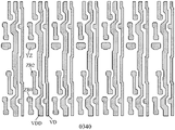
- the source-drain metal layer 0340 of the pixel circuit 0121 is shown, and the source-drain metal layer 0340 is located on the side of the interlayer insulating layer away from the base substrate 10 .
- the source-drain metal layer 0340 may include a first power signal line VDD, a data line VD, a first transfer portion ZB1, a second transfer portion ZB2, and an anode transfer portion YZ.
- each sub-pixel spx includes a first transfer portion ZB1, a second transfer portion ZB2, and an anode transfer portion YZ, respectively.
- the anode transfer part YZ is electrically connected to the conductive region of the active layer of the conduction control transistor through the second via hole GK2 .
- the second via hole GK2 penetrates through the interlayer insulating layer, the interlayer dielectric layer and the gate insulating layer.
- the first end of the first adapter ZB1 is electrically connected to the initialization line VINIT through the through hole TK01
- the second end of the first adapter ZB1 is electrically connected through the through hole.
- TK02 is electrically connected to the source region of the initialization transistor T6 in the active semiconductor layer 0310 (eg, the source region of the initialization transistor T6 in the active semiconductor layer 0310 and the source region of the reset transistor T7 in an integrated structure).
- the through hole TK01 penetrates through the interlayer insulating layer.
- the through hole TK02 penetrates through the interlayer insulating layer, the interlayer dielectric layer and the gate insulating layer.
- the first end of the second transfer portion ZB2 communicates with the drain region of the initialization transistor T6 in the active semiconductor layer 0310 (the drain region of the initialization transistor T6 through the through hole TK03 ).
- the drain region is electrically connected to the gate of the driving transistor
- the second end of the second transfer portion ZB2 is electrically connected to the second pole cc2 of the storage capacitor CST (ie, the gate of the driving transistor) through the through hole TK04.
- the through hole TK03 penetrates through the interlayer insulating layer, the interlayer dielectric layer and the gate insulating layer.
- the through hole TK04 penetrates through the interlayer insulating layer and the interlayer dielectric layer.
- the anode transfer part YZ is electrically connected to the drain region of the second light emitting control circuit 0124 in the active semiconductor layer 0310 through the second via hole GK2 .
- the second via hole GK2 penetrates through the interlayer insulating layer, the interlayer dielectric layer and the gate insulating layer.
- the data line VD is electrically connected to the source region of the data writing transistor T2 in the active semiconductor layer 0310 through the through hole TK05 .
- the through hole TK05 penetrates through the interlayer insulating layer, the interlayer dielectric layer and the gate insulating layer.
- the first power signal line VDD is electrically connected to the source region of the light emitting control transistor T4 in the active semiconductor layer 0310 through the through hole TK06 .
- the through hole TK06 penetrates through the interlayer insulating layer, the interlayer dielectric layer and the gate insulating layer.
- the first power signal line VDD and the data line VD are arranged along the second direction F2, and the first power signal line VDD and the data line VD are roughly along the first direction F1 extension. It should be noted that, in the actual process, due to the limitation of process conditions or other factors such as the arrangement of wiring or via holes, the extension directions of the first power signal line VDD and the data line VD only need to roughly meet the above conditions, which belong to the present invention. the scope of protection of the invention.
- an auxiliary insulating layer may also be formed on the above-mentioned source-drain metal layer 0340 to protect the above-mentioned source-drain metal layer 0340 .
- An auxiliary conductive layer may also be formed on the side of the auxiliary insulating layer away from the base substrate 10, so that the auxiliary conductive layer can be electrically connected to the first power supply signal line VDD to reduce the resistance of the first power supply signal line VDD.
- a first flat layer is formed on the above-mentioned source-drain metal layer 0340 for protecting the above-mentioned source-drain metal layer 0340 .
- a first electrode layer is formed away from the first flat layer.
- the first electrode layer includes an anode located in each sub-pixel. The anode in each sub-pixel is electrically connected to the anode transfer part YZ through the first via hole GK1. Moreover, the first via hole GK1 penetrates through the first flat layer.
- the plurality of sub-pixels includes a first color sub-pixel spx1 and a second color sub-pixel spx2 adjacent along the first direction F1; wherein the first color sub-pixel spx1 includes an anode YG1. , the second color sub-pixel spx2 includes an anode YG2.
- the orthographic projection of the first via hole GK1 in the first color sub-pixel spx1 on the base substrate 1000 is located in the main body part ZT1 in the first color sub-pixel spx1 and the main body part ZT2 in the second color sub-pixel on the base substrate 1000 . between orthographic projections.
- the display panel includes a plurality of repeating units PX; each repeating unit PX includes at least one first color sub-pixel spx1 and at least one second color sub-pixel spx2.
- each repeating unit PX includes a first color sub-pixel spx1 and a second color sub-pixel spx2 adjacent along the first direction F1, and the two adjacent repeating units have two first recesses AX1 and two first overhangs. hole GK1; and, in the first direction F1, two first recesses AX1 and two first via holes GK1 of at least two adjacent repeating units are arranged on the same straight line.
- the first color sub-pixel spx1 is a red sub-pixel
- the second color sub-pixel spx2 is a green sub-pixel
- the red sub-pixel and the green sub-pixel are adjacent along the first direction F1.
- the schematic diagrams of the layout structure of the pixel circuits included in each sub-pixel are arranged in an array along the first direction and the second direction. That is, the layout structure of the pixel circuits included in each sub-pixel is periodically arranged in the row direction and the column direction. Further, a plurality of repeating units PX are arranged along the second direction F2 to form a repeating unit group PXZ, and the repeating unit group PXZ is arranged along the first direction F1. And, the repeating unit includes a first color sub-pixel spx1 and a second color sub-pixel spx2 sequentially arranged along the first direction F1.
- the anode in the second color sub-pixel spx2 faces the anode in the first color sub-pixel spx1 in the orthographic projection of the base substrate 10 and has a first recess AX1 on the orthographic side of the base substrate 10, that is, the first recess AX1 is provided in the main body portion ZT2 in the second color sub-pixel spx2.
- the first color sub-pixel spx1 is a red sub-pixel
- the second color sub-pixel spx2 is a green sub-pixel.
- one repeating unit group PXZ may correspond to one scan line GA, one reset line RST and one light emission control line EM.
- the repeating unit further includes at least one sub-pixel spx3 of the third color.
- the repeat unit may include a third color sub-pixel spx3.
- the connecting lines between the anodes in the adjacent first color sub-pixel spx1, second color sub-pixel spx2 and third color sub-pixel form a triangle.
- the first color sub-pixel spx1 is a red sub-pixel
- the second color sub-pixel spx2 is a green sub-pixel
- the third color sub-pixel spx3 is a blue sub-pixel.
- the red sub-pixel, green sub-pixel and blue sub-pixel The lines between the anodes in the color subpixels form triangles.
- the anode may include a main body portion and a via portion that are electrically connected to each other; wherein the orthographic projection of the via portion on the base substrate 10 covers the first via GK1 on the base substrate. 10, and in each sub-pixel, the via portion is electrically connected to the anode transfer portion YZ through the first via GK1.
- the anode YG1 in the first color sub-pixel spx1 may further include a first connection part LB1 electrically connected between the main body part ZT1 and the via hole part GB1, that is, the main body part ZT1 in the first color sub-pixel spx1 passes through.
- the first connection portion LB1 is electrically connected to the via hole portion GB1.
- the anode YZ2 in the second color sub-pixel spx2 further includes a second connection part LB2 electrically connected between the main body part ZT2 and the via hole part GB2, that is, the main body part ZT2 in the second color sub-pixel spx2 passes through the second connection part LB2 It is electrically connected to the via hole GB2.
- the main body portion ZT3 in the third color sub-pixel spx3 is directly electrically connected to the via hole portion GB3. For example, if the first color sub-pixel spx1 is a red sub-pixel, the main body portion in the red sub-pixel is electrically connected to the via portion through the first connection portion.
- the second color sub-pixel spx2 is a green sub-pixel, and the main body portion in the green sub-pixel is electrically connected to the via portion through the second connection portion.
- the third color sub-pixel spx3 is a blue sub-pixel, and the main body portion in the blue sub-pixel is directly electrically connected to the via portion.
- the first connection portion extends along the first direction F1.
- the second connection portion extends along the third direction F3.
- the third direction F3 is different from the first direction F1 and the second direction F2.
- the third direction F3 has an included angle with the first direction F1 and the second direction F2 respectively, so that the second connecting portion can be extended obliquely upward.
- the main body in the third color sub-pixel spx3 faces the first via GK1 in the second color sub-pixel spx2 on the orthographic projection of the base substrate 10
- the first color sub-pixel spx1 is a red sub-pixel
- the second color sub-pixel spx2 is a green sub-pixel
- the third-color sub-pixel spx3 is a blue sub-pixel.
- the main part of the blue sub-pixel is in The orthographic projection of the base substrate 10 faces the first via hole GK1 in the green sub-pixel and has a second recess AX2 on the orthographic side of the base substrate 10 .
- the orthographic projection of the first via hole GK1 in the first color sub-pixel spx1 on the base substrate 10 is located at the anode YZ1 in the first color sub-pixel spx1. and the anode YZ2 in the second color sub-pixel spx2 is between the orthographic projections of the base substrate 10 .
- the orthographic projection of the first via hole GK1 in the second color sub-pixel spx2 on the base substrate 10 is located in the via hole in the first color sub-pixel spx1
- the portion GB1 and the main body portion ZT3 in the third color sub-pixel spx3 are between the orthographic projections of the base substrate 10 .
- the orthographic projections of the first via hole GK1 in the second color sub-pixel spx2, the via hole portion GB1 in the first color sub-pixel spx1, and the main body portion ZT3 in the third color sub-pixel spx3 on the base substrate 1000 are located at On the same straight line, and the straight line may be substantially parallel to the first direction F1.
- the orthographic projection of the first via hole GK1 in the sub-pixel spx3 of the third color on the base substrate 10 is located in the second recess AX2 on the base substrate 10 .
- the orthographic projection is away from the via portion GB2 in the second color sub-pixel spx2 on the side of the orthographic projection of the base substrate 10 .
- the second color subpixel spx2 is a green subpixel
- the first color subpixel spx1 is a red subpixel
- the third color subpixel spx3 is a blue subpixel.
- the first via hole in the red subpixel The orthographic projection of GK1 on the base substrate 10 is located between the anode in the red sub-pixel and the orthographic projection of the anode in the green sub-pixel on the base substrate 10 .
- the orthographic projection of the first via hole GK1 in the green sub-pixel on the base substrate 10 is located between the orthographic projection of the via hole portion in the red sub-pixel and the main portion of the blue sub-pixel on the base substrate 10 .
- the orthographic projection of the first via hole GK1 in the blue sub-pixel on the base substrate 10 is located in the orthographic projection of the second recess AX2 on the base substrate 10 away from the orthographic projection of the via hole in the green sub-pixel on the base substrate 10 side.
- the orthographic projection of the first recess AX1 of the anode in the second color sub-pixel spx2 in the second direction F2 is the same as that in the first color sub-pixel spx1.
- the orthographic projection of the first via hole GK1 on the second direction F2 at least has an overlapping area; wherein the first direction F1 is different from the second direction F2.
- the first color subpixel spx1 is a red subpixel
- the second color subpixel spx2 is a green subpixel
- the third color subpixel spx3 is a blue subpixel.
- the first color of the anode in the green subpixel is the first
- the orthographic projection of the recess AX1 in the second direction F2 and the orthographic projection of the first via hole GK1 in the red sub-pixel in the second direction F2 at least have an overlapping area.
- the orthographic projection in the second direction F2 refers to the line projection of the anode first recess AX1 of the green sub-pixel and the first via hole GK1 in the red sub-pixel on the straight line where the second direction F2 is located.
- the line projection lengths of the two overlap.
- the orthographic projection in the first direction or the second direction all refers to the line projection on the straight line where the first direction or the second direction is located.
- the orthographic projection of the second recess AX2 of the main body in the third color sub-pixel spx3 in the first direction F1 is the same as that in the second color sub-pixel spx2.
- the orthographic projection of the first via hole GK1 in the first direction F1 at least has an overlapping area.
- the first color sub-pixel spx1 is a red sub-pixel
- the second-color sub-pixel spx2 is a green sub-pixel
- the third-color sub-pixel spx3 is a blue sub-pixel.
- the orthographic projection of the second recess AX2 in the first direction F1 and the orthographic projection of the first via hole GK1 in the green sub-pixel in the first direction F1 at least have an overlapping area.
- the orthographic projection of the first recess AX1 of the anode in the second color sub-pixel spx2 in the second direction F2 covers the first-color sub-pixel spx1 in the orthographic projection.
- the orthographic projection of the first recess AX1 of the anode in the second color subpixel spx2 in the second direction F2 covers the orthographic projection of the via hole GB1 in the first color subpixel spx1 in the second direction F2.
- the first color subpixel spx1 is a red subpixel
- the second color subpixel spx2 is a green subpixel
- the third color subpixel spx3 is a blue subpixel.
- the first color of the anode in the green subpixel is the first
- the orthographic projection of the recess AX1 in the second direction F2 covers the orthographic projection of the first via hole GK1 in the red sub-pixel in the second direction F2.
- the orthographic projection of the second recess AX2 of the main body part ZT3 in the third color sub-pixel spx3 in the first direction F1 covers the second color sub-pixel spx2
- the first color sub-pixel spx1 is a red sub-pixel
- the second color sub-pixel spx2 is a green sub-pixel
- the third color sub-pixel spx3 is a blue sub-pixel.
- the orthographic projection of the recess AX2 in the first direction F1 covers the orthographic projection of the first via hole GK1 in the green sub-pixel in the first direction F1.
- the orthographic projection of the second recess AX2 of the main body part ZT3 in the third color sub-pixel spx3 in the first direction F1 covers the second color sub-pixel spx2
- the first color sub-pixel spx1 is a red sub-pixel
- the second color sub-pixel spx2 is a green sub-pixel
- the third color sub-pixel spx3 is a blue sub-pixel.
- the orthographic projection of the recess AX2 in the first direction F1 covers the orthographic projection of the via hole portion GB2 in the green sub-pixel in the first direction F1.
- the main body part ZT2 in the second color sub-pixel spx2 has a first recess AX1, and in the same repeating unit, the orthographic projection of the first recess AX1 in the second direction F2 covers The orthographic projection of the via portion in the first color sub-pixel spx1 on the second direction F2.
- the second color sub-pixel spx2 is a green sub-pixel
- the first-color sub-pixel spx1 is a red sub-pixel
- the third-color sub-pixel spx3 is a blue sub-pixel
- the main part of the green sub-pixel has the first recess AX1
- the orthographic projection of the first recess AX1 in the second direction F2 covers the orthographic projection of the via portion in the red sub-pixel in the second direction F2.
- the orthographic projection of the second recess AX2 of the main body part ZT3 in the third color sub-pixel spx3 in the first direction F1 covers the second color sub-pixel spx2
- the second color sub-pixel spx2 is a green sub-pixel
- the first color sub-pixel spx1 is a red sub-pixel
- the third-color sub-pixel spx3 is a blue sub-pixel, then in the same repeating unit, the main part of the blue sub-pixel
- the orthographic projection of the second recess AX2 in the first direction F1 covers the orthographic projection of the via portion in the green sub-pixel in the first direction F1.
- the edge of the orthographic projection of the first recess AX1 on the base substrate 10 and the edge of the orthographic projection of the via portion GB1 in the first color sub-pixel spx1 on the base substrate 10 roughly parallel.
- the second color sub-pixel spx2 is a green sub-pixel
- the first color sub-pixel spx1 is a red sub-pixel
- the third color sub-pixel spx3 is a blue sub-pixel.
- the first recess AX1 is in the base substrate 10 .
- the edge of the orthographic projection of is substantially parallel to the edge of the orthographic projection of the via portion in the red sub-pixel on the base substrate 10 . It should be noted that, in the actual process, due to the limitation of process conditions or other factors such as the arrangement of wirings or vias, the above-mentioned parallel relationship only needs to roughly satisfy the above-mentioned conditions, which all belong to the protection scope of the present invention.
- the edge of the orthographic projection of the second recess AX2 on the base substrate 10 is approximately the same as the edge of the orthographic projection of the main body portion ZT2 in the second color sub-pixel spx2 on the base substrate 10 parallel.
- the second color sub-pixel spx2 is a green sub-pixel
- the first color sub-pixel spx1 is a red sub-pixel
- the third-color sub-pixel spx3 is a blue sub-pixel.
- the second recess AX2 is in the base substrate 10 .
- the edge of the orthographic projection of the green sub-pixel is substantially parallel to the edge of the orthographic projection of the main body portion in the green sub-pixel on the base substrate 10 . It should be noted that, in the actual process, due to the limitation of process conditions or other factors such as the arrangement of wirings or vias, the above-mentioned parallel relationship only needs to roughly satisfy the above-mentioned conditions, which all belong to the protection scope of the present invention.
- the edge of the orthographic projection of the first recess AX1 on the base substrate 10 and the edge of the orthographic projection of the via portion ZT1 in the first color sub-pixel spx1 on the base substrate 10 The first distance between them is not less than 2.5 ⁇ m.
- the second color sub-pixel spx2 is a green sub-pixel
- the first-color sub-pixel spx1 is a red sub-pixel
- the third-color sub-pixel spx3 is a blue sub-pixel
- the first recess AX1 is on the edge of the orthographic projection of the base substrate 10
- the first distance from the edge of the orthographic projection of the via portion in the red sub-pixel to the base substrate 10 is not less than 2.5 ⁇ m.
- the first distance between the edge of the orthographic projection of the first recess AX1 on the base substrate 10 and the edge of the orthographic projection of the via portion in the red sub-pixel on the base substrate 10 is 2.5 ⁇ 20 ⁇ m.
- the first distance may be set to 2.5 ⁇ m.
- the first distance may be set to 3.5 ⁇ m, or the first distance may be set to 5.5 ⁇ m, or the first distance may be set to 10 ⁇ m, or the first distance may be set to 20 ⁇ m.
- the first distance can be set to 3.5 ⁇ m when mass-producing the display panel in combination with the precision of the manufacturing process and the equipment.
- the value of the first distance can be set according to the requirements of practical applications, which is not limited here.
- the edge of the orthographic projection of the second recess AX2 on the base substrate 10 and the edge of the orthographic projection of the main body portion ZT2 in the second color sub-pixel spx2 on the base substrate 10 are between.
- the second distance between them is not less than 2.5 ⁇ m.
- the second distance between the edge of the orthographic projection of the second recess AX2 on the base substrate 10 and the edge of the orthographic projection of the main body portion ZT2 in the second color sub-pixel spx2 on the base substrate 10 is 2.5 ⁇ 20 ⁇ m.
- the second color sub-pixel spx2 is a green sub-pixel
- the first-color sub-pixel spx1 is a red sub-pixel
- the third-color sub-pixel spx3 is a blue sub-pixel
- the orthographic projection of the second recess AX2 on the base substrate 10 The second distance between the edge of the green sub-pixel and the edge of the orthographic projection of the via portion in the green sub-pixel on the base substrate 10 is not less than 2.5 ⁇ m. Further, the second distance is 2.5 ⁇ 20 ⁇ m, and the second distance may be set to 2.5 ⁇ m.
- the second distance may be set to 3.5 ⁇ m, or the second distance may be set to 5.5 ⁇ m, or the second distance may be set to 10 ⁇ m, or the second distance may be set to 20 ⁇ m.
- the second distance can be set to 3.5 ⁇ m when the display panel is mass-produced in combination with the precision of the manufacturing process and the equipment.
- the value of the second distance can be set according to the requirements of practical applications, which is not limited here.
- the transistor array layer includes driving transistors located in each sub-pixel.
- the first color sub-pixel spx1 is a red sub-pixel
- the second color sub-pixel spx2 is a green sub-pixel
- the third color sub-pixel spx3 is a blue sub-pixel.
- the channel regions of the driving transistors in the sub-pixels have overlapping regions on the orthographic projection of the base substrate 10 .
- the orthographic projection of the anode in the red sub-pixel on the base substrate 10 does not overlap with the orthographic projection of the channel region of each driving transistor on the base substrate 10 .
- the orthographic projection of the anode in the red sub-pixel on the base substrate 10 and the orthographic projection of the pixel circuit in the red sub-pixel on the base substrate 10 have an overlapping area.
- one repeating unit corresponds to one scan line GA, one reset line RST and one light emission control line EM.
- a repeating unit group PXZ corresponds to a scanning line GA, a reset line RST and a light-emitting control line EM, that is, the pixel circuits in a repeating unit group PXZ are electrically connected to the same scanning line GA, the same reset line RST and the same A luminous control line EM.
- the orthographic projection of the scanning line GA on the base substrate 10 is located between the orthographic projection of the reset line RST and the light emission control line EM on the base substrate 10 between.
- the orthographic projection of the scan lines GA on the base substrate 10 is located at the orthographic projection of the reset lines RST and the luminescence control lines EM on the base substrate 10 between.
- the orthographic projection of the reset line RST on the base substrate 1000 and the anode in the red sub-pixel controlled by the reset line RST are on the base substrate.
- the orthographic projection of 1000 does not overlap
- the orthographic projection of the light emission control line EM on the base substrate 1000 and the orthographic projection of the anode in the green sub-pixel controlled by the light emission control line EM on the base substrate 1000 have an overlapping area
- the scanning line GA has an overlapping area.
- the orthographic projection on the base substrate 1000 does not overlap with the orthographic projection of each anode controlled by the scanning line GA on the base substrate 1000 .
- the orthographic projection of the reset line RST on the base substrate 1000 does not overlap with the orthographic projection of the anode in the red sub-pixel controlled by the reset line RST on the base substrate 1000, and the light emission control line
- the orthographic projection of EM on the base substrate 1000 and the orthographic projection of the anode in the green sub-pixel controlled by the luminescence control line EM on the base substrate 1000 have an overlapping area, and the orthographic projection of the scanning line GA on the base substrate 1000 and the scanning The orthographic projections of the anodes controlled by the line GA on the base substrate 1000 do not overlap.
- the orthographic projection of the light-emitting control line EM controlling the repeating unit on the base substrate 1000 and the orthographic projection of the anode in the blue sub-pixel and the anode in the green sub-pixel on the base substrate 1000 respectively have In the overlapping area, the orthographic projection of the reset line RST and the scanning line GA of the repeating unit on the base substrate 1000 is controlled not to overlap with the orthographic projection of each anode on the base substrate 1000 .
- the reset line RST is a signal line for controlling the initialization transistor T6 and the reset transistor T7 in one repeating unit.
- the light-emitting control line EM is a signal line for controlling the light-emitting control transistor T4 and the turn-on control transistor T5 in one repeating unit.
- the scan line GA is a signal line for controlling the data writing transistor T2 and the threshold compensation transistor T3 in one repeating unit.
- the orthographic projection of the emission control line EM of the repeating unit group PXZ on the base substrate 1000 and the orthographic projection of the anode in the blue sub-pixel and the anode in the green sub-pixel on the base substrate 1000 There are overlapping regions respectively, and the orthographic projections of the reset lines RST and the scanning lines GA of the control repeating unit group PXZ on the base substrate 1000 do not overlap with the orthographic projections of the anodes on the base substrate 1000 .
- the reset line RST is a signal line for controlling the initialization transistor T6 and the reset transistor T7 in one repeating unit group.
- the light-emitting control line EM is a signal line for controlling the light-emitting control transistor T4 and the turn-on control transistor T5 in one repeating unit group.
- the scan line GA is a signal line for controlling the data writing transistor T2 and the threshold compensation transistor T3 in one repeating unit group.
- the orthographic projection of the reset line on the base substrate 10 and the orthographic projection of the anode in the red sub-pixel on the base substrate 10 have an overlapping area, and the light-emitting control line is at
- the orthographic projection of the base substrate 10 and the orthographic projection of the anodes in the green sub-pixels on the base substrate 10 have an overlapping area, and the orthographic projection of the scan lines on the base substrate 10 does not intersect with the orthographic projection of each anode on the base substrate 10 stack.
- the orthographic projection of the anode in the third-color sub-pixel spx3 on the base substrate 10 is respectively related to controlling the reset of the pixel circuit in the third-color sub-pixel spx3.
- the lines and the light emission control lines have overlapping regions on the orthographic projection of the base substrate 10 .
- the first color sub-pixel spx1 is a red sub-pixel
- the second-color sub-pixel spx2 is a green sub-pixel
- the third-color sub-pixel spx3 is a blue sub-pixel.
- the anode in the blue sub-pixel is lining
- the orthographic projections of the base substrate 10 and the orthographic projections of the reset lines and the light emission control lines on the base substrate 10 have overlapping regions, respectively.
- the first via hole GK1 and the second via hole GK2 in the red sub-pixel have a first overlapping area on the orthographic projection of the base substrate 10 .
- the orthographic projection of the first via hole GK1 and the second via hole GK2 in the green sub-pixel has a second overlapping area on the base substrate 10 .
- the orthographic projection of the first via hole GK1 and the second via hole GK2 in the blue sub-pixel has a third overlapping area on the base substrate 10 .
- the area of the first overlapping area is not larger than the area of the second overlapping area.
- the area of the first overlapping area is not larger than that of the third overlapping area.
- the area of the third overlapping region can be made to be substantially equal to that of the second overlapping region. It should be noted that, in the actual process, due to the limitation of process conditions or other factors such as the arrangement of wirings or vias, as long as the above-mentioned equality relationship roughly satisfies the above-mentioned conditions, it belongs to the protection scope of the present invention.
- the area of the first overlapping region is 0 ⁇ 0.9 ⁇ m.
- the area of the first overlapping region may also be 0.5 ⁇ m, or the area of the first overlapping region may also be 0.9 ⁇ m.
- the area of the first overlapping region may be 0, so that the orthographic projections of the first via hole GK1 and the second via hole GK2 in the red sub-pixel on the base substrate 10 do not overlap.
- the area of the second overlapping region is 0 ⁇ 0.9 ⁇ m.
- the area of the second overlapping region may also be 0.5 ⁇ m, or the area of the second overlapping region may also be 0.9 ⁇ m.
- the area of the second overlapping region may be 0, so that the orthographic projections of the first via hole GK1 and the second via hole GK2 in the green sub-pixel on the base substrate 10 do not overlap.
- the area of the third overlapping region is 0 ⁇ 0.9 ⁇ m.
- the area of the third overlapping region may also be 0.5 ⁇ m, or the area of the third overlapping region may also be 0.9 ⁇ m.
- the area of the third overlapping region may be 0, so that the orthographic projections of the first via hole GK1 and the second via hole GK2 in the blue sub-pixel on the base substrate 10 do not overlap.
- the second overlapping area may be set larger. Some to ensure the distance between the anodes in the blue sub-pixel and the green sub-pixel to avoid color mixing.
- the first vias GK1 in adjacent repeating units along the second direction F2 are arranged in sequence approximately along the second direction F2.
- the first vias in the repeating unit group The GK1 are arranged in sequence substantially along the second direction F2.
- the orthographic projections of the first via holes GK1 in the adjacent repeating units along the second direction F2 on the first direction F1 overlap.
- the orthographic projections of the first via hole GK1 in the repeating unit group in the first direction F1 overlap. It should be noted that, in the actual process, due to the limitation of process conditions or other factors such as the arrangement of wirings or vias, the arrangement relationship of the first vias GK1 only needs to roughly satisfy the above conditions, which belong to the protection scope of the present invention.
- a pixel defining layer is formed on the side of the first electrode layer away from the base substrate 10 , and the pixel defining layer includes openings in each sub-pixel, and the same sub-pixel , the orthographic projection of the opening on the base substrate 10 is located within the orthographic projection of the anode on the base substrate 10 .
- the first color sub-pixel spx1 is a red sub-pixel
- the second color sub-pixel spx2 is a green sub-pixel
- the third color sub-pixel spx3 is a blue sub-pixel
- the red sub-pixel has an opening KK1
- the green sub-pixel has an opening KK2
- the blue sub-pixel has an opening KK3. It should be noted that the region where the opening in each sub-pixel is located corresponds to the light-emitting region.
- the orthographic projection of the opening on the base substrate 10 is a rectangle.
- the orthographic projections of the openings in the first color sub-pixel spx1 and the second color sub-pixel spx2 on the base substrate 10 are both rectangles.
- the first color subpixel spx1 is a red subpixel
- the second color subpixel spx2 is a green subpixel
- the third color subpixel spx3 is a blue subpixel
- the orthographic projections of KK2 on the base substrate 10 are all rectangles.
- the area of the opening in the third color sub-pixel spx3 is larger than the area of the opening in the second color sub-pixel spx2, and the opening in the second color sub-pixel spx2 is The area is larger than the area of the opening in the first color sub-pixel spx1.
- the first color subpixel spx1 is a red subpixel
- the second color subpixel spx2 is a green subpixel
- the third color subpixel spx3 is a blue subpixel
- the area of the opening KK3 in the blue subpixel is larger than that of the green subpixel
- the area of the opening KK2 in the green sub-pixel is larger than the area of the opening KK1 in the red sub-pixel.
- the opening area in each sub-pixel can be inversely proportional to the light-emitting life of the sub-pixel.
- the area of the opening in the color sub-pixel is larger than the area of the opening in the green sub-pixel
- the area of the opening in the green sub-pixel is larger than the area of the opening in the red sub-pixel.
- the orthographic projection of the opening on the base substrate 10 faces the first via GK1 in the third color sub-pixel spx3 in the substrate.
- One side of the orthographic projection of the substrate 10 has an opening recess AX0.
- the first color sub-pixel spx1 is a red sub-pixel
- the second color sub-pixel spx2 is a green sub-pixel
- the third-color sub-pixel spx3 is a blue sub-pixel.
- the opening KK3 is in the base substrate 10
- the orthographic projection of the first via hole GK1 has an opening recess AX0 on the side of the orthographic projection of the base substrate 10 .
- the orthographic projection of the opening recess AX0 in the first direction F1 covers the orthographic projection of the first via GK1 in the first direction F1.
- the first color subpixel spx1 is a red subpixel
- the second color subpixel spx2 is a green subpixel
- the third color subpixel spx3 is a blue subpixel.
- the opening recess AX0 is in the first direction
- the orthographic projection on F1 covers the orthographic projection of the first via hole GK1 on the first direction F1.
- the opening recess AX0 is on the edge of the orthographic projection of the base substrate 10 and the first via hole GK1 is on the positive side of the base substrate 10 .
- the projected edges are roughly parallel.
- the first color sub-pixel spx1 is a red sub-pixel
- the second color sub-pixel spx2 is a green sub-pixel
- the third-color sub-pixel spx3 is a blue sub-pixel.
- the opening recess AX0 is in the base substrate.
- the edge of the orthographic projection of 10 is substantially parallel to the edge of the orthographic projection of the first via hole GK1 on the base substrate 10 . It should be noted that, in the actual process, due to the limitation of process conditions or other factors such as the arrangement of wirings or vias, the above-mentioned parallel relationship only needs to roughly satisfy the above-mentioned conditions, which all belong to the protection scope of the present invention.
- the opening recess AX0 is on the edge of the orthographic projection of the base substrate 10 and the first via hole GK1 is on the positive side of the base substrate 10 .
- the third distance between the projected edges is not less than 2.25 ⁇ m. Further, the third distance is 2.25 ⁇ 20 ⁇ m.
- the first color sub-pixel spx1 is a red sub-pixel
- the second color sub-pixel spx2 is a green sub-pixel
- the third-color sub-pixel spx3 is a blue sub-pixel.
- the opening recess AX0 is in the base substrate.
- the third distance between the edge of the orthographic projection of 10 and the edge of the orthographic projection of the first via hole GK1 on the base substrate 10 is not less than 2.25 ⁇ m.
- the third distance may be set to 2.25 ⁇ m.
- the third distance may be set to 2.5 ⁇ m.
- the third distance may be set to 20 ⁇ m.
- the third distance can be set to 2.5 ⁇ m when the display panel is mass-produced in combination with the precision of the fabrication process and the equipment.
- the value of the third distance can be set according to the requirements of practical applications, which is not limited here.
- the main body ZT3 of the anode YG3 faces the first part of the anode YG3 of the third color sub-pixel spx3 in the orthographic projection of the base substrate 1000 .
- a via hole GK1 has a third recess AX3 on the side of the orthographic projection of the base substrate 1000 , and the third recess AX3 is substantially parallel to the opening recess AX0 .
- the first color subpixel spx1 is a red subpixel
- the second color subpixel spx2 is a green subpixel
- the third color subpixel spx3 is a blue subpixel.
- the main body ZT3 of the anode YG3 is in the blue subpixel
- the first via hole GK1 of the orthographic projection of the base substrate 1000 facing the anode YG3 of the third color sub-pixel spx3 has a third recess AX3 on the side of the orthographic projection of the base substrate 1000 , and the third recess AX3 is approximately the same as the opening recess AX0 parallel.
- the edge of the orthographic projection of the third recess AX3 on the base substrate 1000 and the orthographic projection of the opening recess AX0 on the base substrate 1000 overlap.
- the first color subpixel spx1 is a red subpixel
- the second color subpixel spx2 is a green subpixel
- the third color subpixel spx3 is a blue subpixel.
- the third recess AX3 is in the substrate
- the edge of the orthographic projection of the substrate 1000 overlaps the edge of the orthographic projection of the opening recess AX0 on the base substrate 1000 .
- a spacer layer is formed on the side of the pixel defining layer away from the base substrate 10 , and the spacer layer includes a plurality of spacers PS arranged at intervals.
- a spacer PS is disposed between the anodes in the adjacent third sub-pixels along the first direction F1.
- via holes and through holes can be formed in a circle, a square, an octagon, etc., which can be designed according to actual application requirements, which are not limited herein.
- the first color sub-pixel spx1 may also be a green sub-pixel
- the second color sub-pixel spx2 may be a blue sub-pixel.
- the first direction F1 may be the row direction of the sub-pixels
- the second direction F2 may be the column direction of the sub-pixels.
- the repeating unit includes green sub-pixels and blue sub-pixels sequentially arranged along the first direction F1.
- the repeating unit may further include red sub-pixels; wherein, the red sub-pixels and the green sub-pixels are arranged along the second direction F2.
- the anode in the blue sub-pixel faces the anode in the green sub-pixel on the orthographic projection side of the base substrate 10 and has a first recess AX1 on the orthographic side of the base substrate 10 .
- the first via GK1 in the green sub-pixel is The orthographic projection of the base substrate 10 is located between the anode in the green sub-pixel and the anode in the blue sub-pixel in the orthographic projection of the base substrate 10 .
- the first color sub-pixel spx1 is a green sub-pixel
- the second color sub-pixel spx2 is a blue sub-pixel
- the first color of the anode in the blue sub-pixel The orthographic projection of the recess AX1 in the second direction F2 and the orthographic projection of the first via hole GK1 in the green sub-pixel in the second direction F2 at least have an overlapping area.
- the first color sub-pixel spx1 is a green sub-pixel
- the second color sub-pixel spx2 is a blue sub-pixel
- the first color of the anode in the blue sub-pixel The orthographic projection of the recess AX1 in the second direction F2 covers the orthographic projection of the first via hole GK1 in the green sub-pixel in the second direction F2.
- the main body in the blue sub-pixel has a first recess AX1, and
- the orthographic projection of the first recess AX1 in the second direction F2 covers the orthographic projection of the via portion in the green sub-pixel in the second direction F2.
- the first recess AX1 is on the edge of the orthographic projection of the base substrate 10 and the via portion in the green sub-pixel is substantially parallel to the edge of the orthographic projection of the base substrate 10 .
- the first recess AX1 is on the edge of the orthographic projection of the base substrate 10 and
- the first distance between the edges of the orthographic projection of the via portion in the green sub-pixel and the base substrate 10 is not less than 2.5 ⁇ m.
- the first distance may be 2.5 ⁇ 20 ⁇ m.
- the first distance may be 2.5 ⁇ m.
- the first distance may be 3.5 ⁇ m.
- the first distance may also be 20 ⁇ m, which is not limited here.
- the setting method of the red sub-pixel in the repeating unit may refer to the setting method of the red sub-pixel above. This will not be repeated.
- an embodiment of the present disclosure further provides a display device, including the above-mentioned display panel provided by an embodiment of the present disclosure.
- the display device can be any product or component with a display function, such as a mobile phone, a tablet computer, a TV, a monitor, a notebook computer, a digital photo frame, a navigator, and the like.
- Other essential components of the display device should be understood by those of ordinary skill in the art, and will not be repeated here, nor should it be regarded as a limitation of the present disclosure.
Landscapes
- Engineering & Computer Science (AREA)
- Microelectronics & Electronic Packaging (AREA)
- Physics & Mathematics (AREA)
- Geometry (AREA)
- Electroluminescent Light Sources (AREA)
- Devices For Indicating Variable Information By Combining Individual Elements (AREA)
Abstract
Description
Claims (37)
- 一种显示面板,其中,包括:衬底基板,包括多个子像素:晶体管阵列层,位于所述衬底基板上,且所述晶体管阵列层包括位于各所述子像素中的阳极转接部;第一平坦层,位于所述晶体管阵列层背离所述衬底基板一侧;第一电极层,位于所述第一平坦层背离所述衬底基板一侧,所述第一电极层包括位于各所述子像素中的阳极;其中,所述阳极包括相互电连接的主体部与过孔部;且各所述子像素中的过孔部通过第一过孔与所述阳极转接部电连接;所述第一过孔贯穿所述第一平坦层;其中,所述多个子像素包括沿第一方向相邻的第一颜色子像素和第二颜色子像素;所述第一颜色子像素中的第一过孔在所述衬底基板的正投影位于所述第一颜色子像素中的主体部和所述第二颜色子像素中的主体部在所述衬底基板的正投影之间;针对沿所述第一方向相邻的第一颜色子像素和第二颜色子像素,所述第二颜色子像素中的阳极的一边在所述衬底基板的正投影面向所述第一颜色子像素中的阳极在所述衬底基板的正投影一侧具有第一凹陷;且所述第一凹陷朝向所述第二颜色子像素的主体部的中心设置;所述显示面板包括多个重复单元,每个所述重复单元包括至少一个所述第一颜色子像素和至少一个所述第二颜色子像素;相邻的两个所述重复单元至少具有两个所述第一凹陷和两个所述第一过孔;并且,在所述第一方向上,至少相邻的两个所述重复单元具有的两个第一凹陷和第一过孔排列于同一直线上。
- 如权利要求1所述的显示面板,其中,同一所述重复单元中,所述第二颜色子像素中的阳极的第一凹陷在第二方向上的正投影覆盖所述第一颜色子像素中的第一过孔在所述第二方向上的正投影。
- 如权利要求2所述的显示面板,其中,同一所述子像素中,所述过孔部在所述衬底基板的正投影覆盖所述第一过孔在所述衬底基板的正投影;所述第一凹陷设置在所述第二颜色子像素中的主体部,且第一凹陷在所述第二方向上的正投影覆盖所述第一颜色子像素中的过孔部在所述第二方向上的正投影。
- 如权利要求3所述的显示面板,其中,所述第一凹陷在所述衬底基板的正投影的边缘与所述第一颜色子像素中的过孔部在所述衬底基板的正投影的边缘大致平行。
- 如权利要求4所述的显示面板,其中,所述第一凹陷在所述衬底基板的正投影的边缘与所述第一颜色子像素中的过孔部在所述衬底基板的正投影的边缘之间的第一距离为2.5~20μm。
- 如权利要求1-5任一项所述的显示面板,其中,所述第一颜色子像素为红色子像素,所述第二颜色子像素为绿色子像素;所述晶体管阵列层包括位于各所述子像素中的驱动晶体管;所述绿色子像素中的阳极在所述衬底基板的正投影与所述红色子像素中的驱动晶体管的沟道区在所述衬底基板的正投影具有交叠区域。
- 如权利要求6所述的显示面板,其中,所述红色子像素中的阳极在所述衬底基板的正投影与各所述驱动晶体管的沟道区在所述衬底基板的正投影不交叠。
- 如权利要求7所述的显示面板,其中,所述晶体管阵列层包括:相互间隔设置的多条扫描线、多条复位线以及多条发光控制线;其中,一个所述重复单元对应至少一条所述扫描线、至少一条所述复位线以及至少一条所述发光控制线;在一个所述重复单元中,所述复位线在所述衬底基板的正投影与所述复位线控制的所述红色子像素中的阳极在所述衬底基板的正投影不交叠,所述发光控制线在所述衬底基板的正投影与所述发光控制线控制的所述绿色子像素中的阳极在所述衬底基板的正投影具有交叠区域,所述扫描线在所述衬底 基板的正投影与所述扫描线控制的各所述阳极在所述衬底基板的正投影不交叠。
- 如权利要求6-8任一项所述的显示面板,其中,所述晶体管阵列层还包括位于各所述子像素中的导通控制晶体管的有源层;且同一所述子像素中,所述阳极转接部通过第二过孔与所述导通控制晶体管的有源层的导体化区电连接;所述红色子像素中的第一过孔和第二过孔在所述衬底基板的正投影具有第一交叠区域;所述绿色子像素中的第一过孔和第二过孔在所述衬底基板的正投影具有第二交叠区域;所述第一交叠区域的面积不大于所述第二交叠区域的面积。
- 如权利要求9所述的显示面板,其中,所述第一交叠区域的面积为0~0.9μm;所述第二交叠区域的面积为0~0.9μm。
- 如权利要求1-5任一项所述的显示面板,其中,所述第一颜色子像素为绿色子像素,所述第二颜色子像素为蓝色子像素;所述蓝色子像素中的阳极在所述衬底基板的正投影与所述绿色子像素中的驱动晶体管的沟道区在所述衬底基板的正投影具有交叠区域。
- 如权利要求11所述的显示面板,其中,同一所述蓝色子像素中,所述阳极在所述衬底基板的正投影与所述驱动晶体管的沟道区在所述衬底基板的正投影具有交叠区域。
- 如权利要求12所述的显示面板,其中,针对一个所述重复单元,控制所述重复单元的发光控制线在所述衬底基板的正投影与所述蓝色子像素中的阳极和绿色子像素中的阳极在所述衬底基板的正投影分别具有交叠区域,控制所述重复单元的复位线和扫描线在所述衬底基板的正投影与各所述阳极在所述衬底基板的正投影不交叠。
- 如权利要求11-13任一项所述的显示面板,其中,所述绿色子像素中的第一过孔和第二过孔在所述衬底基板的正投影具有第二交叠区域,所述蓝 色子像素中的第一过孔和第二过孔在所述衬底基板的正投影具有第三交叠区域,所述第三交叠区域的面积为0-9μm 2。
- 如权利要求14所述的显示面板,其中,所述第三交叠区域的面积小于等于所述第二交叠区域的面积。
- 如权利要求2-8任一项所述的显示面板,其中,所述重复单元还包括至少一个第三颜色子像素;相邻的所述第一颜色子像素、所述第二颜色子像素以及所述第三颜色子像素中的阳极之间的连线构成三角形。
- 如权利要求16所述的显示面板,其中,同一所述重复单元中,所述第二颜色子像素中的第一过孔在所述衬底基板的正投影位于所述第一颜色子像素中的过孔部与所述第三颜色子像素中的主体部在所述衬底基板的正投影之间,并且所述第二颜色子像素中的第一过孔、所述第一颜色子像素中的过孔部、和所述第三颜色子像素中的主体部在所述衬底基板上的正投影位于同一直线上,所述直线与所述第一方向大致平行。
- 如权利要求17所述的显示面板,其中,同一所述重复单元中,所述第三颜色子像素中的主体部在所述衬底基板的正投影面向所述第二颜色子像素中的第一过孔在所述衬底基板的正投影一侧具有第二凹陷。
- 如权利要求18所述的显示面板,其中,同一所述重复单元中,所述第三颜色子像素中的主体部的第二凹陷在所述第一方向上的正投影与所述第二颜色子像素中的第一过孔在所述第一方向上的正投影至少具有交叠区域。
- 如权利要求19所述的显示面板,其中,同一所述重复单元中,所述第三颜色子像素中的主体部的第二凹陷在所述第一方向上的正投影覆盖所述第二颜色子像素中的第一过孔在所述第一方向上的正投影。
- 如权利要求20所述的显示面板,其中,同一所述重复单元中,所述第三颜色子像素中的主体部的第二凹陷在所述第一方向上的正投影覆盖所述第二颜色子像素中的过孔部在所述第一方向上的正投影。
- 如权利要求21所述的显示面板,其中,所述第二凹陷在所述衬底基 板的正投影的边缘与所述第二颜色子像素中的主体部在所述衬底基板的正投影的边缘大致平行。
- 如权利要求22所述的显示面板,其中,所述第二凹陷在所述衬底基板的正投影的边缘与所述第二颜色子像素中的主体部在所述衬底基板的正投影的边缘之间的第二距离为2.5~20μm。
- 如权利要求16-23任一项所述的显示面板,其中,所述第三颜色子像素中的第一过孔在所述衬底基板的正投影位于所述第二凹陷在所述衬底基板的正投影背离所述第二颜色子像素中的过孔部在所述衬底基板的正投影的一侧。
- 如权利要求3-24任一项所述的显示面板,其中,所述第一颜色子像素中的阳极还包括电连接在主体部和过孔部之间的第一连接部;所述第一连接部沿所述第一方向延伸。
- 如权利要求3-25任一项所述的显示面板,其中,所述第二颜色子像素中的阳极还包括电连接在主体部和过孔部之间的第二连接部;所述第二连接部沿第三方向延伸;所述第三方向与所述第一方向和所述第二方向均不同。
- 如权利要求16-26任一项所述的显示面板,其中,同一所述重复单元中,所述第三颜色子像素中的阳极在所述衬底基板的正投影分别与控制所述重复单元中的像素电路的复位线和发光控制线在所述衬底基板的正投影具有交叠区域。
- 如权利要求16-27任一项所述的显示面板,其中,沿所述第二方向相邻的所述重复单元中的所述第一过孔大致沿第二方向依次排列。
- 如权利要求28所述的显示面板,其中,沿所述第二方向相邻的所述重复单元中的所述第一过孔在第一方向上的正投影重叠。
- 一种显示面板,其中,包括:衬底基板,包括多个子像素:晶体管阵列层,位于所述衬底基板上,且所述晶体管阵列层包括位于各 所述子像素中的阳极转接部;第一平坦层,位于所述晶体管阵列层背离所述衬底基板一侧;第一电极层,位于所述第一平坦层背离所述衬底基板一侧,所述第一电极层包括位于各所述子像素中的阳极,且各所述子像素中的阳极通过第一过孔与所述阳极转接部电连接;所述第一过孔贯穿所述第一平坦层;各所述阳极包括主体部和过孔部;像素限定层,位于所述第一电极层背离所述衬底基板一侧;所述像素限定层包括位于各所述子像素中的开口,且同一所述子像素中,所述开口在所述衬底基板的正投影位于所述阳极在所述衬底基板的正投影内;其中,所述多个子像素包括第三颜色子像素;所述第三颜色子像素中,所述开口在所述衬底基板的正投影面向所述第三颜色子像素中的第一过孔在所述衬底基板的正投影的一侧具有开口凹陷;所述第三颜色子像素中,所述阳极的主体部在所述衬底基板的正投影面向所述第三颜色子像素的阳极的第一过孔在所述衬底基板的正投影的一侧具有第三凹陷,且所述第三凹陷与所述开口凹陷大致平行。
- 如权利要求30所述的显示面板,其中,所述第三颜色子像素中,所述开口凹陷在所述第一方向上的正投影覆盖所述第一过孔在所述第一方向上的正投影。
- 如权利要求31所述的显示面板,其中,所述第三颜色子像素中,所述开口凹陷在所述衬底基板的正投影的边缘与所述第一过孔在所述衬底基板的正投影的边缘大致平行。
- 如权利要求32所述的显示面板,其中,所述第三颜色子像素中,所述开口凹陷在所述衬底基板的正投影的边缘与所述第一过孔在所述衬底基板的正投影的边缘之间的第三距离为2.25~20μm。
- 如权利要求30-33任一项所述的显示面板,其中,所述第三颜色子像素中,所述第三凹陷在所述衬底基板的正投影的边缘与所述开口凹陷在所述衬底基板的正投影的边缘重叠。
- 如权利要求30-34任一项所述的显示面板,其中,所述多个子像素还包括:第一颜色子像素和第二颜色子像素;所述第一颜色子像素和所述第二颜色子像素中的至少一个子像素中,所述开口在所述衬底基板的正投影为矩形。
- 如权利要求35所述的显示面板,其中,所述第三颜色子像素中的开口的面积大于所述第二颜色子像素中的开口的面积;所述第二颜色子像素中的开口的面积大于所述第一颜色子像素中的开口的面积。
- 一种显示装置,其中,包括如权利要求1-36任一项所述的显示面板。
Priority Applications (11)
| Application Number | Priority Date | Filing Date | Title |
|---|---|---|---|
| CN202080002193.8A CN114730796B (zh) | 2020-09-29 | 2020-09-29 | 显示面板及显示装置 |
| PCT/CN2020/119087 WO2022067581A1 (zh) | 2020-09-29 | 2020-09-29 | 显示面板及显示装置 |
| CN202510887484.4A CN120813196A (zh) | 2020-09-29 | 2020-09-29 | 显示面板及显示装置 |
| US17/418,900 US12114544B2 (en) | 2020-09-29 | 2020-09-29 | Display panel and display device with sub-pixel anodes having notches |
| CN202080002490.2A CN115769700B (zh) | 2020-09-29 | 2020-10-27 | 显示面板及显示装置 |
| PCT/CN2020/124166 WO2022067923A1 (zh) | 2020-09-29 | 2020-10-27 | 显示面板及显示装置 |
| US17/424,769 US12069911B2 (en) | 2020-09-29 | 2020-10-27 | Display panel and display apparatus |
| US18/739,494 US12408516B1 (en) | 2020-09-29 | 2024-06-11 | Display panel and display apparatus |
| US18/771,625 US20240365619A1 (en) | 2020-09-29 | 2024-07-12 | Display panel and display device |
| US19/261,751 US20250338726A1 (en) | 2020-09-29 | 2025-07-07 | Display panel and display apparatus |
| US19/267,757 US20250344584A1 (en) | 2020-09-29 | 2025-07-14 | Display panel and display device |
Applications Claiming Priority (1)
| Application Number | Priority Date | Filing Date | Title |
|---|---|---|---|
| PCT/CN2020/119087 WO2022067581A1 (zh) | 2020-09-29 | 2020-09-29 | 显示面板及显示装置 |
Related Child Applications (2)
| Application Number | Title | Priority Date | Filing Date |
|---|---|---|---|
| US17/418,900 A-371-Of-International US12114544B2 (en) | 2020-09-29 | 2020-09-29 | Display panel and display device with sub-pixel anodes having notches |
| US18/771,625 Continuation US20240365619A1 (en) | 2020-09-29 | 2024-07-12 | Display panel and display device |
Publications (1)
| Publication Number | Publication Date |
|---|---|
| WO2022067581A1 true WO2022067581A1 (zh) | 2022-04-07 |
Family
ID=80949417
Family Applications (2)
| Application Number | Title | Priority Date | Filing Date |
|---|---|---|---|
| PCT/CN2020/119087 Ceased WO2022067581A1 (zh) | 2020-09-29 | 2020-09-29 | 显示面板及显示装置 |
| PCT/CN2020/124166 Ceased WO2022067923A1 (zh) | 2020-09-29 | 2020-10-27 | 显示面板及显示装置 |
Family Applications After (1)
| Application Number | Title | Priority Date | Filing Date |
|---|---|---|---|
| PCT/CN2020/124166 Ceased WO2022067923A1 (zh) | 2020-09-29 | 2020-10-27 | 显示面板及显示装置 |
Country Status (3)
| Country | Link |
|---|---|
| US (6) | US12114544B2 (zh) |
| CN (3) | CN114730796B (zh) |
| WO (2) | WO2022067581A1 (zh) |
Cited By (1)
| Publication number | Priority date | Publication date | Assignee | Title |
|---|---|---|---|---|
| WO2024145814A1 (zh) * | 2023-01-04 | 2024-07-11 | 京东方科技集团股份有限公司 | 阵列基板、显示面板及显示装置 |
Families Citing this family (4)
| Publication number | Priority date | Publication date | Assignee | Title |
|---|---|---|---|---|
| WO2022067581A1 (zh) * | 2020-09-29 | 2022-04-07 | 京东方科技集团股份有限公司 | 显示面板及显示装置 |
| KR102839630B1 (ko) * | 2020-12-30 | 2025-07-28 | 엘지디스플레이 주식회사 | 표시 장치 |
| US20230157132A1 (en) * | 2021-01-28 | 2023-05-18 | Boe Technology Group Co., Ltd. | Organic light-emitting display substrate, method for manufacturing the same, and display device |
| CN118872410A (zh) * | 2023-02-28 | 2024-10-29 | 京东方科技集团股份有限公司 | 阵列基板和显示装置 |
Citations (7)
| Publication number | Priority date | Publication date | Assignee | Title |
|---|---|---|---|---|
| US20130176195A1 (en) * | 2012-01-06 | 2013-07-11 | Jungbae Kim | Organic light emitting display device |
| US20140239259A1 (en) * | 2013-02-28 | 2014-08-28 | Samsung Display Co., Ltd. | Organic light-emitting display apparatus |
| US20160285029A1 (en) * | 2015-03-26 | 2016-09-29 | Samsung Display Co., Ltd. | Organic light emitting display apparatus and method of manufacturing same |
| CN107579099A (zh) * | 2017-08-28 | 2018-01-12 | 上海天马微电子有限公司 | 一种显示面板、其制备方法及显示装置 |
| CN107871775A (zh) * | 2017-10-27 | 2018-04-03 | 上海天马有机发光显示技术有限公司 | 一种显示面板及其显示装置 |
| CN110046611A (zh) * | 2019-04-29 | 2019-07-23 | 上海天马微电子有限公司 | 一种显示面板和显示装置 |
| CN111490068A (zh) * | 2019-01-29 | 2020-08-04 | 京东方科技集团股份有限公司 | 显示面板及其制造方法、显示装置 |
Family Cites Families (30)
| Publication number | Priority date | Publication date | Assignee | Title |
|---|---|---|---|---|
| JP5174450B2 (ja) * | 2007-12-18 | 2013-04-03 | パナソニック液晶ディスプレイ株式会社 | 液晶表示装置 |
| KR101378439B1 (ko) * | 2008-08-20 | 2014-03-28 | 삼성디스플레이 주식회사 | 유기 발광 표시 장치 및 그 제조 방법 |
| KR101881852B1 (ko) * | 2011-06-09 | 2018-08-27 | 삼성디스플레이 주식회사 | 표시장치 |
| KR101615332B1 (ko) * | 2012-03-06 | 2016-04-26 | 삼성디스플레이 주식회사 | 유기 발광 표시 장치의 화소 배열 구조 |
| KR101997122B1 (ko) | 2012-07-27 | 2019-07-08 | 삼성디스플레이 주식회사 | 유기 발광 표시 장치 및 이의 제조 방법 |
| KR102096051B1 (ko) * | 2013-03-27 | 2020-04-02 | 삼성디스플레이 주식회사 | 박막 트랜지스터 어레이 기판 및 이를 포함하는 유기 발광 표시 장치 |
| KR102103499B1 (ko) | 2013-10-16 | 2020-04-23 | 삼성디스플레이 주식회사 | 유기 발광 표시 장치 |
| KR102205401B1 (ko) * | 2014-01-14 | 2021-01-21 | 삼성디스플레이 주식회사 | 유기발광표시장치 |
| KR102381288B1 (ko) * | 2015-03-04 | 2022-03-31 | 삼성디스플레이 주식회사 | 유기 발광 표시 장치 |
| KR102561113B1 (ko) * | 2015-08-13 | 2023-07-28 | 삼성디스플레이 주식회사 | 유기 발광 표시 장치 및 그 제조 방법 |
| US11264430B2 (en) * | 2016-02-18 | 2022-03-01 | Chengdu Boe Optoelectronics Technology Co., Ltd. | Pixel arrangement structure with misaligned repeating units, display substrate, display apparatus and method of fabrication thereof |
| KR101919554B1 (ko) * | 2016-04-28 | 2018-11-19 | 삼성디스플레이 주식회사 | 터치 표시 장치 및 이의 제조 방법 |
| CN106444187A (zh) * | 2016-08-22 | 2017-02-22 | 京东方科技集团股份有限公司 | 阵列基板及显示装置 |
| CN106449726B (zh) | 2016-12-27 | 2019-04-26 | 上海天马有机发光显示技术有限公司 | 一种oled显示装置及其制作方法 |
| KR102758391B1 (ko) * | 2016-12-30 | 2025-01-24 | 삼성디스플레이 주식회사 | 표시 장치 |
| CN107170785B (zh) * | 2017-05-26 | 2019-06-25 | 京东方科技集团股份有限公司 | 一种oled显示基板及其制备方法、显示装置 |
| CN107910348B (zh) | 2017-10-26 | 2021-03-16 | 上海天马有机发光显示技术有限公司 | 一种显示面板和显示装置 |
| KR102532307B1 (ko) * | 2017-11-02 | 2023-05-15 | 삼성디스플레이 주식회사 | 표시장치 |
| CN109994509B (zh) * | 2018-01-02 | 2025-01-03 | 京东方科技集团股份有限公司 | 一种像素排布结构及相关装置 |
| CN108846354B (zh) * | 2018-06-11 | 2021-09-14 | 武汉天马微电子有限公司 | 一种显示面板及显示装置 |
| CN109638060B (zh) * | 2018-12-21 | 2020-10-27 | 武汉华星光电半导体显示技术有限公司 | 阵列基板及柔性显示面板 |
| CN109698221B (zh) * | 2018-12-25 | 2021-04-30 | 武汉天马微电子有限公司 | 一种有机发光显示面板及装置 |
| CN110286804B (zh) * | 2019-06-29 | 2023-04-28 | 武汉天马微电子有限公司 | 一种显示面板及显示装置 |
| CN110707134A (zh) | 2019-09-09 | 2020-01-17 | 深圳市华星光电半导体显示技术有限公司 | 阵列基板及显示装置 |
| CN110752243B (zh) | 2019-10-31 | 2023-01-10 | 武汉天马微电子有限公司 | 一种显示面板、其制作方法及显示装置 |
| KR102917273B1 (ko) * | 2019-11-08 | 2026-01-26 | 삼성디스플레이 주식회사 | 표시 장치 및 표시 장치의 제조 방법 |
| CN110993661A (zh) * | 2019-12-02 | 2020-04-10 | 京东方科技集团股份有限公司 | 显示面板及其制作方法、显示装置 |
| CN111463243A (zh) * | 2020-04-09 | 2020-07-28 | 武汉华星光电半导体显示技术有限公司 | 阵列基板及其制备方法 |
| CN111628105B (zh) * | 2020-06-04 | 2023-05-26 | 京东方科技集团股份有限公司 | 显示面板及其制备方法、显示基板及其制备方法和显示装置 |
| WO2022067581A1 (zh) * | 2020-09-29 | 2022-04-07 | 京东方科技集团股份有限公司 | 显示面板及显示装置 |
-
2020
- 2020-09-29 WO PCT/CN2020/119087 patent/WO2022067581A1/zh not_active Ceased
- 2020-09-29 US US17/418,900 patent/US12114544B2/en active Active
- 2020-09-29 CN CN202080002193.8A patent/CN114730796B/zh active Active
- 2020-09-29 CN CN202510887484.4A patent/CN120813196A/zh active Pending
- 2020-10-27 CN CN202080002490.2A patent/CN115769700B/zh active Active
- 2020-10-27 WO PCT/CN2020/124166 patent/WO2022067923A1/zh not_active Ceased
- 2020-10-27 US US17/424,769 patent/US12069911B2/en active Active
-
2024
- 2024-06-11 US US18/739,494 patent/US12408516B1/en active Active
- 2024-07-12 US US18/771,625 patent/US20240365619A1/en active Pending
-
2025
- 2025-07-07 US US19/261,751 patent/US20250338726A1/en active Pending
- 2025-07-14 US US19/267,757 patent/US20250344584A1/en active Pending
Patent Citations (7)
| Publication number | Priority date | Publication date | Assignee | Title |
|---|---|---|---|---|
| US20130176195A1 (en) * | 2012-01-06 | 2013-07-11 | Jungbae Kim | Organic light emitting display device |
| US20140239259A1 (en) * | 2013-02-28 | 2014-08-28 | Samsung Display Co., Ltd. | Organic light-emitting display apparatus |
| US20160285029A1 (en) * | 2015-03-26 | 2016-09-29 | Samsung Display Co., Ltd. | Organic light emitting display apparatus and method of manufacturing same |
| CN107579099A (zh) * | 2017-08-28 | 2018-01-12 | 上海天马微电子有限公司 | 一种显示面板、其制备方法及显示装置 |
| CN107871775A (zh) * | 2017-10-27 | 2018-04-03 | 上海天马有机发光显示技术有限公司 | 一种显示面板及其显示装置 |
| CN111490068A (zh) * | 2019-01-29 | 2020-08-04 | 京东方科技集团股份有限公司 | 显示面板及其制造方法、显示装置 |
| CN110046611A (zh) * | 2019-04-29 | 2019-07-23 | 上海天马微电子有限公司 | 一种显示面板和显示装置 |
Cited By (2)
| Publication number | Priority date | Publication date | Assignee | Title |
|---|---|---|---|---|
| WO2024145814A1 (zh) * | 2023-01-04 | 2024-07-11 | 京东方科技集团股份有限公司 | 阵列基板、显示面板及显示装置 |
| US12469451B2 (en) | 2023-01-04 | 2025-11-11 | Yunnan Invensight Optoelectronics Technology Co., Ltd. | Array base plate, display panel and display device |
Also Published As
| Publication number | Publication date |
|---|---|
| WO2022067923A1 (zh) | 2022-04-07 |
| US20250338726A1 (en) | 2025-10-30 |
| US12069911B2 (en) | 2024-08-20 |
| CN115769700B (zh) | 2025-07-08 |
| US20250344584A1 (en) | 2025-11-06 |
| US20240365619A1 (en) | 2024-10-31 |
| CN114730796B (zh) | 2025-05-27 |
| US20220320194A1 (en) | 2022-10-06 |
| CN120813196A (zh) | 2025-10-17 |
| CN115769700A (zh) | 2023-03-07 |
| US12114544B2 (en) | 2024-10-08 |
| US12408516B1 (en) | 2025-09-02 |
| US20220310753A1 (en) | 2022-09-29 |
| CN114730796A (zh) | 2022-07-08 |
Similar Documents
| Publication | Publication Date | Title |
|---|---|---|
| JP7699060B2 (ja) | ディスプレイパネルおよびディスプレイデバイス | |
| CN112967682B (zh) | 一种显示面板及显示装置 | |
| JP7474786B2 (ja) | ディスプレイパネルおよびディスプレイデバイス | |
| CN114730796B (zh) | 显示面板及显示装置 | |
| US12268062B2 (en) | Display panel and display device with light- emitting devices overlapping winding area | |
| CN113785348B (zh) | 显示面板及显示装置 | |
| US20240315078A1 (en) | Display substrate and display apparatus | |
| CN110910825A (zh) | 一种显示面板及显示装置 | |
| WO2021232411A1 (zh) | 显示基板、显示面板以及显示装置 | |
| WO2022041238A1 (zh) | 一种显示基板及其制作方法、显示装置 | |
| US12232374B2 (en) | Display substrate and display device | |
| US20240008326A1 (en) | Display panel, driving method and display apparatus | |
| CN114766064B (zh) | 显示面板和显示装置 | |
| WO2022041227A1 (zh) | 显示面板及显示装置 | |
| WO2022041237A1 (zh) | 一种显示基板及其制作方法、显示装置 | |
| WO2022041240A1 (zh) | 一种显示基板及其制作方法、显示装置 |
Legal Events
| Date | Code | Title | Description |
|---|---|---|---|
| 121 | Ep: the epo has been informed by wipo that ep was designated in this application |
Ref document number: 20955606 Country of ref document: EP Kind code of ref document: A1 |
|
| NENP | Non-entry into the national phase |
Ref country code: DE |
|
| 32PN | Ep: public notification in the ep bulletin as address of the adressee cannot be established |
Free format text: NOTING OF LOSS OF RIGHTS PURSUANT TO RULE 112(1) EPC (EPO FORM 1205 DATED 07/07/2023) |
|
| 122 | Ep: pct application non-entry in european phase |
Ref document number: 20955606 Country of ref document: EP Kind code of ref document: A1 |
|
| WWG | Wipo information: grant in national office |
Ref document number: 202080002193.8 Country of ref document: CN |