WO2021235288A1 - Power circuit device - Google Patents
Power circuit device Download PDFInfo
- Publication number
- WO2021235288A1 WO2021235288A1 PCT/JP2021/018016 JP2021018016W WO2021235288A1 WO 2021235288 A1 WO2021235288 A1 WO 2021235288A1 JP 2021018016 W JP2021018016 W JP 2021018016W WO 2021235288 A1 WO2021235288 A1 WO 2021235288A1
- Authority
- WO
- WIPO (PCT)
- Prior art keywords
- power circuit
- transformer
- circuit device
- transformers
- substrate
- Prior art date
- Legal status (The legal status is an assumption and is not a legal conclusion. Google has not performed a legal analysis and makes no representation as to the accuracy of the status listed.)
- Ceased
Links
Images


Classifications
-
- H—ELECTRICITY
- H01—ELECTRIC ELEMENTS
- H01F—MAGNETS; INDUCTANCES; TRANSFORMERS; SELECTION OF MATERIALS FOR THEIR MAGNETIC PROPERTIES
- H01F27/00—Details of transformers or inductances, in general
- H01F27/08—Cooling; Ventilating
-
- H—ELECTRICITY
- H01—ELECTRIC ELEMENTS
- H01F—MAGNETS; INDUCTANCES; TRANSFORMERS; SELECTION OF MATERIALS FOR THEIR MAGNETIC PROPERTIES
- H01F30/00—Fixed transformers not covered by group H01F19/00
- H01F30/06—Fixed transformers not covered by group H01F19/00 characterised by the structure
- H01F30/10—Single-phase transformers
-
- H—ELECTRICITY
- H02—GENERATION; CONVERSION OR DISTRIBUTION OF ELECTRIC POWER
- H02M—APPARATUS FOR CONVERSION BETWEEN AC AND AC, BETWEEN AC AND DC, OR BETWEEN DC AND DC, AND FOR USE WITH MAINS OR SIMILAR POWER SUPPLY SYSTEMS; CONVERSION OF DC OR AC INPUT POWER INTO SURGE OUTPUT POWER; CONTROL OR REGULATION THEREOF
- H02M3/00—Conversion of DC power input into DC power output
- H02M3/22—Conversion of DC power input into DC power output with intermediate conversion into AC
- H02M3/24—Conversion of DC power input into DC power output with intermediate conversion into AC by static converters
- H02M3/28—Conversion of DC power input into DC power output with intermediate conversion into AC by static converters using discharge tubes with control electrode or semiconductor devices with control electrode to produce the intermediate AC
Definitions
- This disclosure relates to a power circuit device.
- the transformer device described in Patent Document 1 Japanese Unexamined Patent Publication No. 2013-51258, is referred to as two printed wiring boards (hereinafter, "first printed wiring board” and “second printed wiring board”, respectively. ) And a plurality of transformers.
- the first printed wiring board and the second printed wiring board are arranged facing each other with a gap.
- the plurality of transformers are arranged in a matrix between the first printed wiring board and the second printed wiring board.
- the spacing between the columns of two adjacent transformers in the row direction is constant along the column direction.
- the present disclosure provides a power circuit device capable of enhancing the cooling uniformity for each transformer.
- the power circuit device of the present disclosure is arranged between the first substrate and the second substrate, which are spaced apart from each other in the first direction, and between the first substrate and the second substrate, and is the first. It comprises a plurality of first transformers arranged so as to form a first row inclined with respect to a second direction orthogonal to one direction.
- the power circuit device of the present disclosure it is possible to improve the uniformity of cooling for each transformer.
- power circuit device 100 (First Embodiment)
- power circuit device 100 the configuration of the power circuit device (hereinafter referred to as “power circuit device 100”) according to the first embodiment will be described.
- FIG. 1 is a circuit diagram of the power circuit device 100. As shown in FIG. 1, the power circuit device 100 includes a primary side circuit 10, a secondary side circuit 20, and a transformer 30. The power circuit device 100 constitutes a DC / DC converter.
- the primary side circuit 10 includes a ground terminal 11, an input terminal 12, an input side switching element 13a, an input side switching element 13b, an input side switching element 13c, an input side switching element 13d, and an input capacitor 14. doing.
- the ground terminal 11 is grounded.
- the input terminal 12, the input voltage V in of the power circuit 100 is applied.
- the input side switching element 13a, the input side switching element 13b, the input side switching element 13c, and the input side switching element 13d are, for example, MOSFETs (Metal Oxide Field Effect Transistors).
- the input side switching element 13a, the input side switching element 13b, the input side switching element 13c, and the input side switching element 13d may be IGBTs (Insulated Gate Bipolar Transistors).
- the input side switching element 13a, the input side switching element 13b, the input side switching element 13c, and the input side switching element 13d are formed on, for example, a silicon (Si) substrate.
- the input side switching element 13a, the input side switching element 13b, the input side switching element 13c, and the input side switching element 13d may be formed on a substrate made of silicon carbide (SiC) or gallium nitride (GaN).
- Each of the input side switching element 13a, the input side switching element 13b, the input side switching element 13c, and the input side switching element 13d has a drain, a source, and a gate.
- the drain of the input side switching element 13a is connected to the input terminal 12.
- the drain of the input side switching element 13b is connected to the source of the input side switching element 13a.
- the source of the input-side switching element 13b is connected to the ground terminal 11.
- the drain of the input side switching element 13c is connected to the input terminal 12.
- the drain of the input side switching element 13d is connected to the source of the input side switching element 13c.
- the source of the input-side switching element 13d is connected to the ground terminal 11.
- the gates of the input side switching element 13a, the input side switching element 13b, the input side switching element 13c, and the input side switching element 13d are connected to a control circuit (not shown).
- the input capacitor 14 is connected to the ground terminal 11 and the input terminal 12 so as to be in parallel with the input side switching element 13a and the input side switching element 13b (input side switching element 13c and input side switching element 13d).
- the secondary circuit 20 includes a ground terminal 21, an output terminal 22, an output side rectifying element 23a, an output side rectifying element 23b, an output side rectifying element 23c, an output side rectifying element 23d, and an output capacitor 24.
- the ground terminal 21 is grounded.
- the output voltage V out of the power circuit device 100 is output from the output terminal 22.
- the output side rectifying element 23a, the output side rectifying element 23b, the output side rectifying element 23c, and the output side rectifying element 23d are, for example, Schottky barrier diodes.
- the output-side rectifying element 23a, the output-side rectifying element 23b, the output-side rectifying element 23c, and the output-side rectifying element 23d are formed on, for example, a substrate made of silicon, silicon carbide, or gallium nitride.
- the output side rectifying element 23a, the output side rectifying element 23b, the output side rectifying element 23c, and the output side rectifying element 23d have a cathode and an anode.
- the cathode of the output side rectifying element 23a is connected to the output terminal 22.
- the cathode of the output side rectifying element 23b is connected to the anode of the output side rectifying element 23a.
- the anode of the output side rectifying element 23b is connected to the ground terminal 21.
- the cathode of the output side rectifying element 23c is connected to the output terminal 22.
- the cathode of the output side rectifying element 23d is connected to the anode of the output side rectifying element 23c.
- the anode of the output side rectifying element 23d is connected to the ground terminal 21.
- the output capacitor 24 is connected to the ground terminal 21 and the output terminal 22 so as to be in parallel with the output side rectifying element 23a and the output side rectifying element 23b (output side rectifying element 23c and output side rectifying element 23d).
- the transformer 30 is composed of a plurality of transformers that can be regarded as one transformer as an equivalent circuit.
- the transformer 30 is composed of, for example, a transformer 31a to a transformer 31e, a transformer 32a to a transformer 32e, a transformer 33a to a transformer 33e, a transformer 34a to a transformer 34e, a transformer 35a to a transformer 35e, and a transformer 36a to a transformer 36e. ing.
- the transformer 31a has a primary coil 37a, a secondary coil 37b, and a core 38.
- the primary coil 37a and the secondary coil 37b are magnetically coupled by the core 38.
- the primary side coil 37a and the secondary side coil 37b are conductive materials (for example, metal materials such as copper (Cu), gold (Au), copper alloy, nickel (Ni) alloy, gold alloy, silver (Ag) alloy, etc.). It is a winding formed by.
- the core 38 is, for example, a ferrite core such as manganese (Mn) -zinc (Zn) -based ferrite, nickel-zinc-based ferrite, an amorphous core, or an iron dust core.
- the primary coil 37a and the secondary coil 37b pass through a hole formed in the core 38.
- the core 38 may be an EI type core.
- the core 38 may be an EE type core, a U type core, an ER type core, or an ER type core.
- the transformer 31a may be an outer iron type planar transformer. When the transformer 31a is an outer iron type planar transformer, the heat dissipation of the transformer 31a is improved.
- the transformer 31a may be a transformer using a toroidal core. When the transformer 31a is a transformer using a toroidal core, the heat dissipation of the core 38 is improved.
- Each of the transformers 31b to 31e, the transformers 32a to 32e, the transformers 33a to 33e, the transformers 34a to 34e, the transformers 35a to 35e, and the transformers 36a to 36e have the same configurations as the transformer 31a, for example. ing.
- One end of the primary coil 37a of the transformers 31a to 31e is connected to the source of the input-side switching element 13a and the drain of the input-side switching element 13b.
- the other ends of the primary coil 37a of the transformers 31a to 31e are connected to one end of the primary coils 37a of the transformers 32a to 32e, respectively.
- the other ends of the primary coil 37a of the transformers 32a to 32e are connected to one end of the primary coils 37a of the transformers 33a to 33e, respectively.
- the other end of the primary coil 37a of the transformer 33a to 33e is connected to one end of the primary coil 37a of the transformer 34a to 34e, respectively.
- the other ends of the primary coil 37a of the transformers 34a to 34e are connected to one end of the primary coils 37a of the transformers 35a to 35e, respectively.
- the other ends of the primary coil 37a of the transformers 35a to 35e are connected to one end of the primary coils 37a of the transformers 36a to 36e, respectively.
- the other end of the primary coil 37a of the transformers 36a to 36e is connected to the source of the input-side switching element 13c and the drain of the input-side switching element 13d.
- One end of the secondary coil 37b of the transformers 31a to 31e is connected to the anode of the output side rectifying element 23a and the cathode of the output side rectifying element 23b.
- the other ends of the secondary coil 37b of the transformers 31a to 31e are connected to one end of the secondary coils 37b of the transformers 32a to 32e, respectively.
- the other ends of the secondary coil 37b of the transformers 32a to 32e are connected to one end of the secondary coils 37b of the transformers 33a to 33e, respectively.
- the other end of the secondary coil 37b of the transformers 33a to 33e is connected to one end of the secondary coil 37b of the transformers 34a to 34a, respectively.
- the other end of the secondary coil 37b of the transformers 34a to 34e is connected to one end of the secondary coil 37b of the transformers 35a to 35e, respectively.
- the other end of the secondary coil 37b of the transformers 35a to 35e is connected to one end of the secondary coil 37b of the transformers 36a to 36e, respectively.
- the other end of the secondary coil 37b of the transformers 36a to 36e is connected to the anode of the output side rectifying element 23c and the cathode of the output side rectifying element 23d.
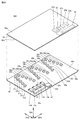
- FIG. 2A is an exploded perspective view of the power circuit device 100.
- the output side rectifying element 23a to the output side rectifying element 23d, the output terminal 22, and the output capacitor 24 are shown by dotted lines.
- FIG. 2B is a perspective view of the power circuit device 100.
- FIG. 2C is a perspective view of the power circuit device 100 in which the second substrate 50 is transparently displayed.
- the power circuit device 100 further includes a first substrate 40 and a second substrate 50.
- the first substrate 40 has a first surface 40a and a second surface 40b.
- the first surface 40a and the second surface 40b are the main surfaces of the first substrate 40.
- the second surface 40b is the opposite surface of the first surface 40a.
- the second substrate 50 has a first surface 50a and a second surface 50b.
- the first surface 50a and the second surface 50b are the main surfaces of the second substrate 50.
- the second surface 50b is the opposite surface of the first surface 50a.
- the first substrate 40 and the second substrate 50 are arranged at intervals in the first direction DR1 so that the first surface 40a and the second surface 50b face each other.
- the ground terminal 11 (not shown in FIGS. 2A to 2C), the input terminal 12, the input side switching element 13a to the input side switching element 13d, and the input capacitor 14 are arranged on the first surface 40a.
- the ground terminal 21 (not shown in FIGS. 2A to 2C), the output terminal 22, the output side rectifying element 23a to the output side rectifying element 23d, and the output capacitor 24 are arranged on the second surface 50b.
- the transformer 30 (transformer 31a to transformer 31e, transformer 32a to transformer 32e, transformer 33a to transformer 33e, transformer 34a to transformer 34e, transformer 35a to transformer 35e, and transformer 36a to transformer 36e) includes the first substrate 40 and the second substrate 50. (More specifically, between the first surface 40a and the second surface 50b).
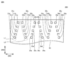
- FIG. 3A is a plan view of the power circuit device 100.
- the illustration of the second substrate 50 is omitted.
- the transformers 31a to 31e are arranged so as to form an inclined row (hereinafter, referred to as “first row L1”) with respect to the second direction DR2.
- the transformers 32a to 32e are arranged so as to form an inclined row (hereinafter referred to as "second row L2") with respect to the second direction DR2.
- the second direction DR2 is a direction orthogonal to the first direction DR1.
- the transformers 31a to 31e are arranged in this order from one side in the second direction DR2 (corresponding to the upper side in FIG. 3A) to the other side in the second direction DR2 (corresponding to the lower side in FIG. 3A). ing.
- the transformers 32a to 32e are arranged in this order from one side in the second direction DR2 toward the other side in the second direction DR2.
- the cooling air for cooling the transformer 30 is blown from the other side in the second direction DR2 to one side in the second direction DR2.
- the transformers 31a to 31e are arranged to face each other at a distance from the transformers 32a to 32e in the third direction DR3.
- the third direction DR3 is a direction orthogonal to the first direction DR1 and the second direction DR2.
- the distance between the transformer 31b and the transformer 32b in the third direction DR3 is wider than the distance between the transformer 31a and the transformer 32a in the third direction DR3.
- the distance between the transformer 31c and the transformer 32c in the third direction DR3 is wider than the distance between the transformer 31b and the transformer 32b in the third direction DR3.
- the distance between the transformer 31d and the transformer 32d in the third direction DR3 is wider than the distance between the transformer 31c and the transformer 32c in the third direction DR3.
- the distance between the transformer 31e and the transformer 32e in the third direction DR3 is wider than the distance between the transformer 31d and the transformer 32d in the third direction DR3.
- the distance between the first row L1 and the second row L2 in the third direction DR3 increases from one side in the second direction DR2 toward the other side in the second direction DR2. , Is spreading. That is, the distance between the first row L1 and the second row L2 in the third direction DR3 increases as it approaches the source of the cooling air.
- the transformers 33a to 33e and the transformers 35a to 35e are arranged so as to form the first row L1 respectively. Further, the transformers 34a to 34e and the transformers 36a to 36e are arranged so as to form the second row L2, respectively.
- FIG. 3B is a plan view of the power circuit device 100 according to the first modification.
- FIG. 3C is a plan view of the power circuit device 100 according to the second modification.
- the first row L1 and the second row L2 do not have to be linear in a plan view.
- the distance in the third direction DR3 between the transformers belonging to two adjacent first row L1s (belonging to the second row L2) is from one side to the second in the second direction DR2. It may become smaller (see FIG. 3B) or larger (see FIG. 3C) toward the other side in the direction DR2.
- FIG. 3D is a plan view of the power circuit device 100 according to the third modification.
- FIG. 3E is a plan view of the power circuit device 100 according to the fourth modification.
- the first row L1 and the second row L2 may be inclined in the same direction. In this case, the distance between the first row L1 and the second row L2 in the third direction DR3 does not widen from one side in the second direction DR2 toward the other side in the second direction DR2.
- wiring is formed on the first substrate 40 and the second substrate 50.
- the input terminal 12, the input side switching element 13a to the input side switching element 13d, the input capacitor 14, the ground terminal 21, the output terminal 22, the output side rectifying element 23a to the output side rectifying element 23d, the output capacitor 24 and the transformer 30. are connected as shown in FIG.
- the wiring of the primary circuit 10 is formed on the first substrate 40.
- the wiring of the secondary circuit 20 is formed on the second substrate 50.
- the first substrate 40 and the second substrate 50 may be formed with a solid pattern (a copper foil pattern that fills a large area) as a ground pattern at a portion where the above wiring is not formed.
- FIG. 4A is a side view of the power circuit device 100 when viewed along the third direction DR3.
- FIG. 4B is a side view of the power circuit device 100 when viewed along the second direction DR2.
- the transformers (transformers 32a to 32e) belonging to the second row L2 are the transformers (transformers) belonging to the first row L1 respectively. It is in a position overlapping with 31a to 31e).
- the transformers belonging to the first row L1 are positioned at different positions from each other, and the transformers belonging to the second row L2 are located.
- the second direction DR2 is a direction in which the transformers belonging to the first row L1 (second row L2) appear to be offset from each other
- the third direction DR3 is in the second row L2. This is the direction in which the transformer to which it belongs appears to overlap the transformer belonging to the first column L1.
- the power circuit device 100 is not limited to the DC / DC converter.
- the power circuit device 100 may be a circuit device including a transformer other than the DC / DC converter. Further, the above-mentioned number of rows and columns in the transformer 30 is an example.
- power circuit device 200 the power circuit device 200 according to the comparative example.
- the power circuit device 200 includes a primary side circuit 10, a secondary side circuit 20, a transformer 30, a first board 40, and a second board 50. In this respect, the configuration of the power circuit device 200 is common to the configuration of the power circuit device 100.
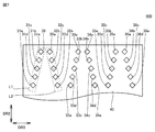
- FIG. 5 is a plan view of the power circuit device 200.
- the illustration of the second substrate 50 is omitted.
- the transformers 31a to 31e are arranged so as to form a row (hereinafter referred to as “third row L3”) along the second direction DR2.
- the transformers 32a to 32e, the transformers 33a to 33e, the transformers 34a to 34e, the transformers 35a to 35e, and the transformers 36a to 36e are arranged so as to form the third row L3, respectively.
- the configuration of the power circuit device 200 is different from the configuration of the power circuit device 100.
- the transformers 31a to 31e, the transformers 32a to 32e, the transformers 33a to 33e, the transformers 34a to 34e, the transformers 35a to 35e, and the transformers 36a to 36e are located along the second direction DR2. Since they are arranged so as to form three rows L3, the cooling air supplied to the transformer is on the other side of the second direction DR2 from the transformer (that is, at a position closer to the source of the cooling air than the transformer). (There is) It is easy to be disturbed by other transformers. As a result, the cooling effect of the cooling air becomes smaller as the transformer is on one side in the second direction DR2.
- the first row L1 and the second row L2 are inclined with respect to the second direction DR2, and between the first row L1 and the second row L2 in the third direction DR3. Since the interval extends from one side in the second direction DR2 toward the other side in the second direction DR2, the cooling air supplied to the transformer included in the first row L1 (second row L2) is in the first row. It is less likely to be disturbed by another transformer included in L1 and located on the other side of the second direction DR2 than the transformer.
- the distance between the first row L1 and the second row L2 in the third direction DR3 is from one side to the second in the second direction DR2. Although it does not extend toward the other side in the direction DR2, it is included in the first row L1 (second row L2) because the first row L1 (second row L2) is inclined with respect to the second direction DR2.
- the cooling air supplied to the transformer is contained in the first row L1 and is less likely to be obstructed by another transformer located on the other side of the second direction DR2 than the transformer.
- the power circuit device 100 it is possible to improve the uniformity of cooling for each transformer. Further, as a result of increasing the cooling uniformity for each transformer, the power circuit device 100 can be further miniaturized and operated at a higher temperature.
- the first board 40 and the second board 50 function as ducts. As a result, the cooling air can be supplied to the transformer 30 without being dissipated. Since the power circuit device 100 has a structure in which the transformer 30 is sandwiched between the first board 40 and the second board 50, the strength of the device can be increased.
- the wiring of the primary side circuit 10 and the wiring of the secondary side circuit 20 are mixed on one board. As a result, the substrate area increases. However, in the power circuit device 100, since the wiring of the primary side circuit 10 and the wiring of the secondary side circuit 20 are formed on the first board 40 and the second board 50, respectively, the area of each board is reduced. This makes it possible to reduce the size of the device. Further, in the power circuit device 100, as a result of the wiring of the primary side circuit 10 and the wiring of the secondary side circuit 20 being formed on the first board 40 and the second board 50, respectively, the wiring is simplified and the wiring impedance is increased. The resulting noise can be reduced.
- the solid pattern When a solid pattern (a copper foil pattern that fills a large area) is formed on the first substrate 40 and the second substrate 50 as a ground pattern, the solid pattern functions as an electromagnetic shield by sandwiching the power circuit.
- the amount of noise emitted to the outside and the amount of noise received from the outside can be reduced, and the noise resistance of the power circuit device 100 is improved. Further, in this case, the amount of the etching solution consumed in producing the first substrate 40 and the second substrate 50 can be reduced, so that the production cost can be reduced.
- power circuit device 300 the configuration of the power circuit device (hereinafter referred to as “power circuit device 300”) according to the second embodiment will be described.
- the points different from the configuration of the power circuit device 100 will be mainly described, and the duplicated description will not be repeated.
- the power circuit device 300 has a primary side circuit 10, a secondary side circuit 20, a transformer 30, a first board 40, and a second board 50.
- the transformers 31a to 31e, the transformers 33a to 33e, and the transformers 35a to 35e are arranged so as to form the first row L1.
- the transformers 32a to 32e, the transformers 34a to 34e, and the transformers 36a to 36e are arranged so as to form the second row L2, respectively.
- the configuration of the power circuit device 300 is common to the configuration of the power circuit device 100.
- FIG. 6 is a plan view of the power circuit device 300.
- the input terminal 12, the input side switching element 13a to the input side switching element 13d, the input capacitor 14, the ground terminal 21, the output terminal 22, the output side rectifying element 23a to the output side rectifying element 23d, the output capacitor 24, and The illustration of the second substrate 50 is omitted.
- the distance in the second direction DR2 between two adjacent transformers increases from the other side in the second direction DR2 toward one side in the second direction DR2. That is, the distance in the second direction DR2 between two adjacent transformers increases as the distance from the source of the cooling air increases.
- the configuration of the power circuit device 300 is different from the configuration of the power circuit device 100.
- the distance between the two adjacent transformers in the second direction DR2 increases as the distance from the source of the cooling air increases, so that the distance from the source of the cooling air increases, the more the cooling air passes through.
- the possible routes are widening. Therefore, in the power circuit device 300, it becomes easier to supply the cooling air to the transformer located at a position away from the source of the cooling air, so that the uniformity of cooling for each transformer can be further improved.
- power circuit device 400 the configuration of the power circuit device (hereinafter referred to as “power circuit device 400”) according to the third embodiment will be described.
- the points different from the configuration of the power circuit device 100 will be mainly described, and the duplicated description will not be repeated.
- the power circuit device 400 has a primary side circuit 10, a secondary side circuit 20, a transformer 30, a first board 40, and a second board 50.
- the transformers 31a to 31e, the transformers 33a to 33e, and the transformers 35a to 35e are arranged so as to form the first row L1.
- the transformers 32a to 32e, the transformers 34a to 34e, and the transformers 36a to 36e are arranged so as to form the second row L2, respectively.
- the configuration of the power circuit device 400 is common to the configuration of the power circuit device 100.
- FIG. 7 is a plan view of the power circuit device 400.
- the illustration of the second substrate 50 is omitted.
- each transformer included in the transformer 30 has a side surface 39.
- Each transformer included in the transformer 30 is arranged so that the side surface 39 is inclined with respect to the second direction DR2. That is, each of the transformers included in the transformer 30 is arranged so that the side surface 39 is inclined with respect to the direction of the cooling air.
- the configuration of the power circuit device 400 is different from the configuration of the power circuit device 100.
- the power circuit device 400 since the side surface 39 is inclined with respect to the direction of the cooling air, turbulence is unlikely to occur when the side surface 39 and the cooling air collide with each other. As a result, according to the power circuit device 400, it becomes easier to supply the cooling air to the transformers located at a position away from the source of the cooling air, so that the uniformity of cooling for each transformer can be further improved.
- power circuit device 500 the configuration of the power circuit device (hereinafter referred to as “power circuit device 500”) according to the fourth embodiment will be described.
- the points different from the configuration of the power circuit device 100 will be mainly described, and the duplicated description will not be repeated.
- the power circuit device 500 includes a primary side circuit 10, a secondary side circuit 20, a transformer 30, a first board 40, and a second board 50.
- the transformers 31a to 31e, the transformers 33a to 33e, and the transformers 35a to 35e are arranged so as to form the first row L1.
- the transformers 32a to 32e, the transformers 34a to 34e, and the transformers 36a to 36e are arranged so as to form the second row L2, respectively.
- the configuration of the power circuit device 500 is common to the configuration of the power circuit device 100.
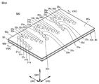
- FIG. 8A is a perspective view of the power circuit device 500.
- FIG. 8B is a plan view of the power circuit device 500.
- FIG. 8C is a cross-sectional view of the power circuit device 500.
- FIG. 8C shows cross sections at positions corresponding to VIIIC-VIIIC in FIGS. 8A and 8B.
- the first substrate 40 is formed with a through hole 40c that penetrates the first substrate 40 in the thickness direction.
- the second substrate 50 is formed with a through hole 50c that penetrates the second substrate 50 in the thickness direction.
- the through hole 40c and the through hole 50c are formed at positions overlapping with each of the transformers included in the transformer 30 in a plan view.
- the power circuit device 500 further includes a resin member 60 and a resin member 70. In these respects, the configuration of the power circuit device 500 is different from the configuration of the power circuit device 100.
- the resin member 60 has a first portion 61, a second portion 62, and a third portion 63.
- the first portion 61 is on the first surface 40a and is in contact with each of the transformers included in the transformer 30. That is, each transformer included in the transformer 30 is adhered to the first substrate 40 by the resin member 60.
- the second portion 62 is on the second surface 40b.
- the third portion 63 is arranged in the through hole 40c and connects the first portion 61 and the second portion 62.
- the outer diameter of the resin member 60 in the first portion 61 and the second portion 62 is larger than the inner diameter of the through hole 40c.
- the resin member 70 has the same configuration as the resin member 60.
- the resin member 70 has a first portion 71, a second portion 72, and a third portion 73.
- the first portion 71 is on the second surface 50b and is in contact with each transformer included in the transformer 30 (each transformer included in the transformer 30 is adhered to the second substrate 50 by the resin member 70). Yes).
- the second portion 72 is on the first surface 50a.
- the third portion 73 is arranged in the through hole 50c and connects the first portion 71 and the second portion 72.
- the outer diameter of the resin member 70 in the first portion 71 and the second portion 72 is larger than the inner diameter of the through hole 50c.
- the resin member 60 and the resin member 70 are made of a resin material.
- the resin material is, for example, polypropylene (PP), acrylonitrile butadiene styrene (ABS), polyethylene terephthalate (PET), polycarbonate (PC), fluororesin, phenol resin, melamine resin, polyurethane, epoxy resin, silicone and the like.
- the resin member 60 and the resin member 70 may be formed of polybutylene terephthalate (PBT), polyphenylene sulfide (PPS), polyetheretherketone (PEEK), or the like containing a heat conductive filler.
- PBT polybutylene terephthalate
- PPS polyphenylene sulfide
- PEEK polyetheretherketone
- the heat generated in each of the transformers included in the transformer 30 is released to the surrounding space via the resin member 60 (resin member 70) and the first substrate 40 (second substrate 50). It will be. Therefore, according to the power circuit device 500, the heat dissipation performance is improved.
- each transformer included in the transformer 30 is adhered to the first substrate 40 (second substrate 50) by the resin member 60 (resin member 70). Therefore, according to the power circuit device 500, the impact resistance can be improved.
Landscapes
- Engineering & Computer Science (AREA)
- Power Engineering (AREA)
- Dc-Dc Converters (AREA)
- Transformer Cooling (AREA)
Abstract
Description
本開示は、電力回路装置に関する。 This disclosure relates to a power circuit device.
特許文献1(特開2013-51258号公報)に記載されているトランス装置は、2枚の印刷配線基板(以下においては、それぞれ「第1印刷配線基板」及び「第2印刷配線基板」とする)と、複数のトランスとを有している。 The transformer device described in Patent Document 1 (Japanese Unexamined Patent Publication No. 2013-51258) is referred to as two printed wiring boards (hereinafter, "first printed wiring board" and "second printed wiring board", respectively. ) And a plurality of transformers.
第1印刷配線基板及び第2印刷配線基板は、間隔を空けて対向配置されている。複数のトランスは、第1印刷配線基板と第2印刷配線基板との間において、マトリクス状に配列されている。行方向において隣り合う2つのトランスの列の間の間隔は、列方向に沿って一定となっている。 The first printed wiring board and the second printed wiring board are arranged facing each other with a gap. The plurality of transformers are arranged in a matrix between the first printed wiring board and the second printed wiring board. The spacing between the columns of two adjacent transformers in the row direction is constant along the column direction.
特許文献1に記載されているトランス装置においては、列方向における一方側から列方向における他方側に向かって冷却風が供給される際、トランスに供給される冷却風は、当該トランスよりも列方向における一方側にある別のトランスにより遮られやすいため、当該冷却風により冷却されがたい。すなわち、特許文献1に記載されているトランス装置においては、各々のトランスが均一に冷却されがたい。 In the transformer device described in Patent Document 1, when the cooling air is supplied from one side in the row direction to the other side in the row direction, the cooling air supplied to the transformer is in the row direction rather than the transformer. It is difficult to be cooled by the cooling air because it is easily blocked by another transformer on one side of the above. That is, in the transformer device described in Patent Document 1, it is difficult to uniformly cool each transformer.
本開示は、各々のトランスに対する冷却の均一性を高めることが可能な電力回路装置を提供するものである。 The present disclosure provides a power circuit device capable of enhancing the cooling uniformity for each transformer.
本開示の電力回路装置は、第1方向において互いに間隔を空けて対向配置されている第1基板及び第2基板と、第1基板と第2基板との間に配置されており、かつ、第1方向に直交している第2方向に対して傾斜している第1列をなすように配列されている複数の第1トランスとを備える。 The power circuit device of the present disclosure is arranged between the first substrate and the second substrate, which are spaced apart from each other in the first direction, and between the first substrate and the second substrate, and is the first. It comprises a plurality of first transformers arranged so as to form a first row inclined with respect to a second direction orthogonal to one direction.
本開示の電力回路装置によると、各々のトランスに対する冷却の均一性を高めることが可能となる。 According to the power circuit device of the present disclosure, it is possible to improve the uniformity of cooling for each transformer.
本開示の実施形態の詳細を、図面を参照しながら説明する。以下の図面においては、同一又は相当する部分に同一の参照符号を付し、重複する説明は繰り返さないものとする。 The details of the embodiments of the present disclosure will be described with reference to the drawings. In the following drawings, the same or corresponding parts shall be designated with the same reference numerals, and duplicate explanations shall not be repeated.
(第1実施形態)
以下に、第1実施形態に係る電力回路装置(以下においては、「電力回路装置100」とする)の構成を説明する。
(First Embodiment)
Hereinafter, the configuration of the power circuit device (hereinafter referred to as “
図1は、電力回路装置100の回路図である。図1に示されるように、電力回路装置100は、一次側回路10と、二次側回路20と、トランス30とを有している。電力回路装置100は、DC/DCコンバータを構成している。
FIG. 1 is a circuit diagram of the
一次側回路10は、接地端子11と、入力端子12と、入力側スイッチング素子13aと、入力側スイッチング素子13bと、入力側スイッチング素子13cと、入力側スイッチング素子13dと、入力コンデンサ14とを有している。
The
接地端子11は、接地されている。入力端子12には、電力回路装置100の入力電圧Vinが印加される。
The
入力側スイッチング素子13a、入力側スイッチング素子13b、入力側スイッチング素子13c及び入力側スイッチング素子13dは、例えばMOSFET(Metal Oxide Field Effect Transistor)である。入力側スイッチング素子13a、入力側スイッチング素子13b、入力側スイッチング素子13c及び入力側スイッチング素子13dは、IGBT(Insulated Gate Bipolar Transistor)であってもよい。
The input
入力側スイッチング素子13a、入力側スイッチング素子13b、入力側スイッチング素子13c及び入力側スイッチング素子13dは、例えばシリコン(Si)の基板に形成されている。入力側スイッチング素子13a、入力側スイッチング素子13b、入力側スイッチング素子13c及び入力側スイッチング素子13dは、炭化珪素(SiC)又は窒化ガリウム(GaN)の基板に形成されていてもよい。
The input
入力側スイッチング素子13a、入力側スイッチング素子13b、入力側スイッチング素子13c及び入力側スイッチング素子13dの各々は、ドレインと、ソースと、ゲートとを有している。
Each of the input
入力側スイッチング素子13aのドレインは、入力端子12に接続されている。入力側スイッチング素子13bのドレインは、入力側スイッチング素子13aのソースに接続されている。入力側スイッチング素子13bのソースは、接地端子11に接続されている。
The drain of the input
入力側スイッチング素子13cのドレインは、入力端子12に接続されている。入力側スイッチング素子13dのドレインは、入力側スイッチング素子13cのソースに接続されている。入力側スイッチング素子13dのソースは、接地端子11に接続されている。
The drain of the input
入力側スイッチング素子13a、入力側スイッチング素子13b、入力側スイッチング素子13c及び入力側スイッチング素子13dのゲートは、制御回路(図示せず)に接続される。
The gates of the input
入力コンデンサ14は、入力側スイッチング素子13a及び入力側スイッチング素子13b(入力側スイッチング素子13c及び入力側スイッチング素子13d)と並列になるように、接地端子11と入力端子12とに接続されている。
The
二次側回路20は、グランド端子21と、出力端子22と、出力側整流素子23aと、出力側整流素子23bと、出力側整流素子23cと、出力側整流素子23dと、出力コンデンサ24とを有している。
The
グランド端子21は、グランドされている。出力端子22からは、電力回路装置100の出力電圧Voutが出力される。
The
出力側整流素子23a、出力側整流素子23b、出力側整流素子23c及び出力側整流素子23dは、例えばショットキーバリアダイオードである。出力側整流素子23a、出力側整流素子23b、出力側整流素子23c及び出力側整流素子23dは、例えばシリコン、炭化珪素又は窒化ガリウムの基板に形成されている。
The output side rectifying
出力側整流素子23a、出力側整流素子23b、出力側整流素子23c及び出力側整流素子23dは、カソードと、アノードとを有している。出力側整流素子23aのカソードは、出力端子22に接続されている。出力側整流素子23bのカソードは、出力側整流素子23aのアノードに接続されている。出力側整流素子23bのアノードは、グランド端子21に接続されている。出力側整流素子23cのカソードは、出力端子22に接続されている。出力側整流素子23dのカソードは、出力側整流素子23cのアノードに接続されている。出力側整流素子23dのアノードは、グランド端子21に接続されている。
The output side rectifying
出力コンデンサ24は、出力側整流素子23a及び出力側整流素子23b(出力側整流素子23c及び出力側整流素子23d)と並列になるように、グランド端子21と出力端子22とに接続されている。
The
トランス30は、等価回路として1つのトランスと見做せる複数のトランスにより構成されている。トランス30は、例えば、トランス31a~トランス31eと、トランス32a~トランス32eと、トランス33a~トランス33eと、トランス34a~トランス34eと、トランス35a~トランス35eと、トランス36a~トランス36eとにより構成されている。
The
トランス31aは、一次側コイル37aと、二次側コイル37bと、コア38とを有している。一次側コイル37aと二次側コイル37bとは、コア38により磁気結合されている。
The
一次側コイル37a及び二次側コイル37bは、導電性材料(例えば、銅(Cu)、金(Au)、銅合金、ニッケル(Ni)合金、金合金、銀(Ag)合金等の金属材料)により形成されている巻線である。
The
コア38は、例えばマンガン(Mn)-亜鉛(Zn)系フェライト、ニッケル-亜鉛系フェライト等のフェライトコア、アモルファスコア又はアイアンダストコアである。一次側コイル37a及び二次側コイル37bは、コア38に形成されている穴の中を通っている。コア38は、EI型コアであってもよい。コア38は、EE型コア、U型コア、EER型コア又はER型コアであってもよい。
The
トランス31aは、外鉄形のプレーナトランスであってもよい。トランス31aが外鉄形のプレーナトランスである場合、トランス31aの放熱性が向上する。トランス31aは、トロイダルコアを用いたトランスであってもよい。トランス31aがトロイダルコアを用いたトランスである場合、コア38の放熱性が向上する。
The
トランス31b~トランス31e、トランス32a~トランス32e、トランス33a~トランス33e、トランス34a~トランス34e、トランス35a~トランス35e及びトランス36a~トランス36eの各々は、例えば、トランス31aと同様の構成を有している。
Each of the
トランス31a~トランス31eの一次側コイル37aの一方端は、入力側スイッチング素子13aのソース及び入力側スイッチング素子13bのドレインに接続されている。トランス31a~トランス31eの一次側コイル37aの他方端は、それぞれ、トランス32a~トランス32eの一次側コイル37aの一方端に接続されている。トランス32a~トランス32eの一次側コイル37aの他方端は、それぞれ、トランス33a~トランス33eの一次側コイル37aの一方端に接続されている。
One end of the
トランス33a~トランス33eの一次側コイル37aの他方端は、それぞれ、トランス34a~トランス34eの一次側コイル37aの一方端に接続されている。トランス34a~トランス34eの一次側コイル37aの他方端は、それぞれ、トランス35a~トランス35eの一次側コイル37aの一方端に接続されている。
The other end of the
トランス35a~トランス35eの一次側コイル37aの他方端は、それぞれ、トランス36a~トランス36eの一次側コイル37aの一方端に接続されている。トランス36a~トランス36eの一次側コイル37aの他方端は、入力側スイッチング素子13cのソース及び入力側スイッチング素子13dのドレインに接続されている。
The other ends of the
トランス31a~トランス31eの二次側コイル37bの一方端は、出力側整流素子23aのアノード及び出力側整流素子23bのカソードに接続されている。トランス31a~トランス31eの二次側コイル37bの他方端は、それぞれ、トランス32a~トランス32eの二次側コイル37bの一方端に接続されている。トランス32a~トランス32eの二次側コイル37bの他方端は、それぞれ、トランス33a~トランス33eの二次側コイル37bの一方端に接続されている。
One end of the
トランス33a~トランス33eの二次側コイル37bの他方端は、それぞれ、トランス34a~トランス34aの二次側コイル37bの一方端に接続されている。トランス34a~トランス34eの二次側コイル37bの他方端は、それぞれ、トランス35a~トランス35eの二次側コイル37bの一方端に接続されている。
The other end of the
トランス35a~トランス35eの二次側コイル37bの他方端は、それぞれ、トランス36a~トランス36eの二次側コイル37bの一方端に接続されている。トランス36a~トランス36eの二次側コイル37bの他方端は、出力側整流素子23cのアノード及び出力側整流素子23dのカソードに接続されている。
The other end of the
図2Aは、電力回路装置100の分解斜視図である。図2A中において、出力側整流素子23a~出力側整流素子23d、出力端子22及び出力コンデンサ24は、点線により示されている。図2Bは、電力回路装置100の斜視図である。図2Cは、第2基板50を透過表示させた電力回路装置100の斜視図である。図2A、図2B及び図2Cに示されるように、電力回路装置100は、第1基板40と、第2基板50とをさらに有している。
FIG. 2A is an exploded perspective view of the
第1基板40は、第1面40aと、第2面40bとを有している。第1面40a及び第2面40bは、第1基板40の主面である。第2面40bは、第1面40aの反対面である。第2基板50は、第1面50aと、第2面50bとを有している。第1面50a及び第2面50bは、第2基板50の主面である。第2面50bは、第1面50aの反対面である。第1基板40及び第2基板50は、第1面40aと第2面50bとが互いに対向するように、第1方向DR1において間隔を空けて配置されている。
The
接地端子11(図2A~図2C中において図示せず)、入力端子12、入力側スイッチング素子13a~入力側スイッチング素子13d及び入力コンデンサ14は、第1面40a上に配置されている。グランド端子21(図2A~図2C中において図示せず)、出力端子22、出力側整流素子23a~出力側整流素子23d及び出力コンデンサ24は、第2面50b上に配置されている。
The ground terminal 11 (not shown in FIGS. 2A to 2C), the
トランス30(トランス31a~トランス31e、トランス32a~トランス32e、トランス33a~トランス33e、トランス34a~トランス34e、トランス35a~トランス35e及びトランス36a~トランス36e)は、第1基板40と第2基板50との間(より具体的には、第1面40aと第2面50bとの間)に配置されている。
The transformer 30 (
図3Aは、電力回路装置100の平面図である。図3A中においては、入力端子12、入力側スイッチング素子13a~入力側スイッチング素子13d、入力コンデンサ14、グランド端子21、出力端子22、出力側整流素子23a~出力側整流素子23d、出力コンデンサ24及び第2基板50の図示が省略されている。図3Aに示されるように、トランス31a~トランス31eは、第2方向DR2に対して傾斜している列(以下においては、「第1列L1」とする)をなすように配列されている。
FIG. 3A is a plan view of the
トランス32a~トランス32eは、第2方向DR2に対して傾斜している列(以下においては、「第2列L2」とする)をなすように配列されている。第2方向DR2は、第1方向DR1に直交している方向である。
The
トランス31a~トランス31eは、第2方向DR2における一方側(図3A中の上側に対応)から第2方向DR2における他方側(図3A中の下側に対応)に向かって、この順で配列されている。トランス32a~トランス32eは、第2方向DR2における一方側から第2方向DR2における他方側に向かって、この順で配列されている。なお、図示されていないが、トランス30を冷却するための冷却風は、第2方向DR2における他方側から第2方向DR2における一方側へと送風される。
The
トランス31a~トランス31eは、第3方向DR3において、トランス32a~トランス32eとそれぞれ間隔を空けて対向配置されている。第3方向DR3は、第1方向DR1及び第2方向DR2に直交している方向である。
The
第3方向DR3におけるトランス31bとトランス32bとの間の間隔は、第3方向DR3におけるトランス31aとトランス32aとの間の間隔よりも広い。第3方向DR3におけるトランス31cとトランス32cとの間の間隔は、第3方向DR3におけるトランス31bとトランス32bとの間の間隔よりも広い。
The distance between the
第3方向DR3におけるトランス31dとトランス32dとの間の間隔は、第3方向DR3におけるトランス31cとトランス32cとの間の間隔よりも広い。第3方向DR3におけるトランス31eとトランス32eとの間の間隔は、第3方向DR3におけるトランス31dとトランス32dとの間の間隔よりも広い。
The distance between the
このことを別の観点から言えば、第3方向DR3における第1列L1と第2列L2との間の間隔は、第2方向DR2における一方側から第2方向DR2における他方側に向かうにしたがって、拡がっている。すなわち、第3方向DR3における第1列L1と第2列L2との間の間隔は、冷却風の発生源に近づくにつれて、拡がっている。 From another point of view, the distance between the first row L1 and the second row L2 in the third direction DR3 increases from one side in the second direction DR2 toward the other side in the second direction DR2. , Is spreading. That is, the distance between the first row L1 and the second row L2 in the third direction DR3 increases as it approaches the source of the cooling air.
トランス33a~トランス33e及びトランス35a~トランス35eは、それぞれ第1列L1をなすように配列されている。また、トランス34a~トランス34e及びトランス36a~トランス36eは、それぞれ第2列L2をなすように配列されている。
The
図3Bは、第1変形例に係る電力回路装置100の平面図である。図3Cは、第2変形例に係る電力回路装置100の平面図である。図3B及び図3C中において、入力端子12、入力側スイッチング素子13a~入力側スイッチング素子13d、入力コンデンサ14、グランド端子21、出力端子22、出力側整流素子23a~出力側整流素子23d、出力コンデンサ24及び第2基板50の図示が省略されている。図3B及び図3Cに示されるように、第1列L1及び第2列L2は、平面視において、直線状でなくてもよい。
FIG. 3B is a plan view of the
このことを別の観点から言えば、隣り合う2つの第1列L1に属する(第2列L2に属する)トランスの間の第3方向DR3における間隔が、第2方向DR2における一方側から第2方向DR2における他方側に向かうにしたがって、小さくなっていてもよく(図3B参照)、大きくなっていてもよい(図3C参照)。 From another point of view, the distance in the third direction DR3 between the transformers belonging to two adjacent first row L1s (belonging to the second row L2) is from one side to the second in the second direction DR2. It may become smaller (see FIG. 3B) or larger (see FIG. 3C) toward the other side in the direction DR2.
図3Dは、第3変形例に係る電力回路装置100の平面図である。図3Eは、第4変形例に係る電力回路装置100の平面図である。図3D及び図3E中において、入力端子12、入力側スイッチング素子13a~入力側スイッチング素子13d、入力コンデンサ14、グランド端子21、出力端子22、出力側整流素子23a~出力側整流素子23d、出力コンデンサ24及び第2基板50の図示が省略されている。図3D及び図3Eに示されるように、第1列L1及び第2列L2は、同一方向に傾斜していてもよい。この場合、第3方向DR3における第1列L1と第2列L2との間の間隔は、第2方向DR2における一方側から第2方向DR2における他方側に向かうにしたがって拡がっていない。
FIG. 3D is a plan view of the
図示されていないが、第1基板40及び第2基板50には、配線が形成されている。この配線により、入力端子12、入力側スイッチング素子13a~入力側スイッチング素子13d、入力コンデンサ14、グランド端子21、出力端子22、出力側整流素子23a~出力側整流素子23d、出力コンデンサ24及びトランス30は、図1に示されるように接続されている。一次側回路10の配線は、第1基板40に形成されている。二次側回路20の配線は、第2基板50に形成されている。なお、第1基板40及び第2基板50には、上記の配線が形成されていない箇所において、グランドパターンとして、べたパターン(大面積を塗りつぶすような銅箔パターン)が形成されていてもよい。
Although not shown, wiring is formed on the
図4Aは、第3方向DR3に沿って見た際の電力回路装置100の側面図である。図4Bは、第2方向DR2に沿って見た際の電力回路装置100の側面図である。図4Aに示されるように、第3方向DR3に沿って電力回路装置100を見ると、第2列L2に属するトランス(トランス32a~トランス32e)は、それぞれ、第1列L1に属するトランス(トランス31a~トランス31e)に重なる位置にある。他方で、図4Bに示されるように、第2方向DR2に沿って電力回路装置100を見ると、第1列L1に属するトランスの各々は互いにずれた位置にあり、第2列L2に属するトランスの各々は互いにずれた位置にある。このことを別の観点から言えば、第2方向DR2は、第1列L1(第2列L2)に属するトランスの各々が互いにずれて見える方向であり、第3方向DR3は第2列L2に属するトランスが第1列L1に属するトランスに重なって見える方向である。
FIG. 4A is a side view of the
上記において、電力回路装置100の例として、DC/DCコンバータを説明したが、電力回路装置100は、DC/DCコンバータに限られない。電力回路装置100は、DC/DCコンバータ以外のトランスを含む回路装置であってもよい。また、トランス30における上記の行段数及び列段数は、例示である。
Although the DC / DC converter has been described above as an example of the
以下に、電力回路装置100の効果を、比較例に係る電力回路装置(以下「電力回路装置200」とする)と対比しながら説明する。
Hereinafter, the effect of the
電力回路装置200は、一次側回路10と、二次側回路20と、トランス30と、第1基板40と、第2基板50とを有している。この点に関して、電力回路装置200の構成は、電力回路装置100の構成と共通している。
The
図5は、電力回路装置200の平面図である。図5中においては、入力端子12、入力側スイッチング素子13a~入力側スイッチング素子13d、入力コンデンサ14、グランド端子21、出力端子22、出力側整流素子23a~出力側整流素子23d、出力コンデンサ24及び第2基板50の図示が省略されている。図5に示されるように、トランス31a~トランス31eは、第2方向DR2に沿う列(以下においては、「第3列L3」という)をなすように配列されている。
FIG. 5 is a plan view of the
トランス32a~トランス32e、トランス33a~トランス33e、トランス34a~トランス34e、トランス35a~トランス35e及びトランス36a~トランス36eは、それぞれ、第3列L3をなすように配列されている。この点に関して、電力回路装置200の構成は、電力回路装置100の構成と異なっている。
The
電力回路装置200では、トランス31a~トランス31e、トランス32a~トランス32e、トランス33a~トランス33e、トランス34a~トランス34e、トランス35a~トランス35e及びトランス36a~トランス36eがそれぞれ第2方向DR2に沿う第3列L3をなすように配列されているため、トランスに供給される冷却風が当該トランスよりも第2方向DR2における他方側にある(つまり、当該トランスよりも冷却風の発生源に近い位置にある)他のトランスにより妨げられやすい。その結果、第2方向DR2における一方側にあるトランスほど、冷却風による冷却効果が小さくなる。
In the
他方で、電力回路装置100では、第1列L1及び第2列L2が第2方向DR2に対して傾斜しているとともに、第3方向DR3における第1列L1と第2列L2との間の間隔が第2方向DR2における一方側から第2方向DR2における他方側に向かって拡がっているため、第1列L1(第2列L2)に含まれるトランスに供給される冷却風は、第1列L1に含まれ、かつ当該トランスよりも第2方向DR2における他方側に位置する他のトランスにより妨げられにくい。
On the other hand, in the
なお、第3変形例及び第4変形例に係る電力回路装置100においては、第3方向DR3における第1列L1と第2列L2との間の間隔が第2方向DR2における一方側から第2方向DR2における他方側に向かって拡がっていないが、第1列L1(第2列L2)が第2方向DR2に対して傾斜しているため、第1列L1(第2列L2)に含まれるトランスに供給される冷却風は、第1列L1に含まれ、かつ当該トランスよりも第2方向DR2における他方側に位置する他のトランスにより妨げられにくい。
In the
このように、電力回路装置100によると、各々のトランスに対する冷却の均一性を高めることが可能となる。また、各々のトランスに対する冷却の均一性が高められる結果、電力回路装置100をさらに小型化すること及びさらに高温で動作させることが可能となる。
As described above, according to the
電力回路装置100においては、トランス30が第1基板40と第2基板50とに挟み込まれているため、第1基板40及び第2基板50がダクトとして機能する。その結果、冷却風を散逸させることなくトランス30に供給することができる。電力回路装置100は、トランス30が第1基板40と第2基板50に挟み込まれた構造を有しているため、装置の強度を高めることができる。
In the
電力回路装置100を1枚の基板に実装する場合、1枚の基板に一次側回路10の配線と二次側回路20の配線が混在することになる。その結果、基板面積が増大してしまう。しかしながら、電力回路装置100においては、一次側回路10の配線及び二次側回路20の配線をそれぞれ第1基板40及び第2基板50に形成しているため、各々の基板の面積を縮小することができ、装置の小型化が可能となる。また、電力回路装置100においては、一次側回路10の配線及び二次側回路20の配線がそれぞれ第1基板40及び第2基板50に形成されている結果、配線が簡易になり、配線インピーダンスに起因したノイズを低減することができる。
When the
第1基板40及び第2基板50にグランドパターンとしてべたパターン(大面積を塗りつぶすような銅箔パターン)が形成されている場合、当該べたパターンが電力回路を挟み込むことにより電磁シールドとして機能するため、外部に放出するノイズ量及び外部から受けるノイズ量を低減することができ、電力回路装置100の耐ノイズ性が向上する。また、この場合、第1基板40及び第2基板50を生産する上で消費されるエッチング液の量を低減することができるため、生産コストを低下させることが可能となる。
When a solid pattern (a copper foil pattern that fills a large area) is formed on the
(第2実施形態)
以下に、第2実施形態に係る電力回路装置(以下においては、「電力回路装置300」とする)の構成を説明する。ここでは、電力回路装置100の構成と異なる点を主に説明し、重複する説明は繰り返さない。
(Second Embodiment)
Hereinafter, the configuration of the power circuit device (hereinafter referred to as “
電力回路装置300は、一次側回路10と、二次側回路20と、トランス30と、第1基板40と、第2基板50とを有している。トランス31a~トランス31e、トランス33a~トランス33e及びトランス35a~トランス35eは、それぞれ第1列L1をなすように配列されている。トランス32a~トランス32e、トランス34a~トランス34e及びトランス36a~トランス36eは、それぞれ第2列L2をなすように配列されている。これらの点に関して、電力回路装置300の構成は、電力回路装置100の構成と共通している。
The
図6は、電力回路装置300の平面図である。図6中においては、入力端子12、入力側スイッチング素子13a~入力側スイッチング素子13d、入力コンデンサ14、グランド端子21、出力端子22、出力側整流素子23a~出力側整流素子23d、出力コンデンサ24及び第2基板50の図示が省略されている。図6に示されるように、隣り合う2つのトランスの間の第2方向DR2における間隔は、第2方向DR2における他方側から第2方向DR2における一方側に向かうにしたがって、拡がっている。すなわち、隣り合う2つのトランスの間の第2方向DR2における間隔は、冷却風の発生源から遠ざかるにつれて、拡がっている。この点に関して、電力回路装置300の構成は、電力回路装置100の構成と異なっている。
FIG. 6 is a plan view of the
以下に、電力回路装置300の効果を説明する。ここでは、電力回路装置100の効果と異なる点を主に説明し、重複する説明は繰り返さないものとする。
The effect of the
電力回路装置300においては、隣り合う2つのトランスの第2方向DR2における間の間隔が冷却風の発生源から遠ざかるにつれて拡がっているため、冷却風の発生源から遠ざかるほど、冷却風が通り抜けることのできる経路が広くなっている。そのため、電力回路装置300においては、冷却風の発生源から離れた位置にあるトランスに冷却風をさらに供給しやすくなるため、各々のトランスに対する冷却の均一性をさらに高めることが可能となる。
In the
(第3実施形態)
以下に、第3実施形態に係る電力回路装置(以下においては、「電力回路装置400」とする)の構成を説明する。ここでは、電力回路装置100の構成と異なる点を主に説明し、重複する説明は繰り返さない。
(Third Embodiment)
Hereinafter, the configuration of the power circuit device (hereinafter referred to as “
電力回路装置400は、一次側回路10と、二次側回路20と、トランス30と、第1基板40と、第2基板50とを有している。トランス31a~トランス31e、トランス33a~トランス33e及びトランス35a~トランス35eは、それぞれ第1列L1をなすように配列されている。トランス32a~トランス32e、トランス34a~トランス34e及びトランス36a~トランス36eは、それぞれ第2列L2をなすように配列されている。これらの点に関して、電力回路装置400の構成は、電力回路装置100の構成と共通している。
The
図7は、電力回路装置400の平面図である。図7中においては、入力端子12、入力側スイッチング素子13a~入力側スイッチング素子13d、入力コンデンサ14、グランド端子21、出力端子22、出力側整流素子23a~出力側整流素子23d、出力コンデンサ24及び第2基板50の図示が省略されている。
FIG. 7 is a plan view of the
図7に示されるように、トランス30に含まれる各々のトランスは、側面39を有している。トランス30に含まれる各々のトランスは、側面39が第2方向DR2に対して傾斜するように配置されている。すなわち、トランス30に含まれる各々のトランスは、側面39が冷却風の方向に対して傾斜するように配置されている。この点に関して、電力回路装置400の構成は、電力回路装置100の構成と異なっている。
As shown in FIG. 7, each transformer included in the
以下に、電力回路装置400の効果を説明する。ここでは、電力回路装置100の効果と異なる点を主に説明し、重複する説明は繰り返さないものとする。
The effect of the
電力回路装置400においては、側面39が冷却風の方向に対して傾斜しているため、側面39と冷却風とが衝突した際に、乱流が発生しにくい。その結果、電力回路装置400によると、冷却風の発生源から離れた位置にあるトランスに冷却風をさらに供給しやすくなるため、各々のトランスに対する冷却の均一性をさらに高めることが可能となる。
In the
(第4実施形態)
以下に、第4実施形態に係る電力回路装置(以下においては、「電力回路装置500」とする)の構成を説明する。ここでは、電力回路装置100の構成と異なる点を主に説明し、重複する説明は繰り返さない。
(Fourth Embodiment)
Hereinafter, the configuration of the power circuit device (hereinafter referred to as “
電力回路装置500は、一次側回路10と、二次側回路20と、トランス30と、第1基板40と、第2基板50とを有している。トランス31a~トランス31e、トランス33a~トランス33e及びトランス35a~トランス35eは、それぞれ第1列L1をなすように配列されている。トランス32a~トランス32e、トランス34a~トランス34e及びトランス36a~トランス36eは、それぞれ第2列L2をなすように配列されている。これらの点に関して、電力回路装置500の構成は、電力回路装置100の構成と共通している。
The
図8Aは、電力回路装置500の斜視図である。図8Bは、電力回路装置500の平面図である。図8Cは、電力回路装置500の断面図である。図8Cには、図8A中及び図8B中のVIIIC-VIIICに対応した位置における断面が示されている。図8Cに示されるように、第1基板40には、第1基板40を厚さ方向に貫通している貫通穴40cが形成されている。第2基板50には、第2基板50を厚さ方向に貫通している貫通穴50cが形成されている。貫通穴40c及び貫通穴50cは、平面視において、トランス30に含まれる各々のトランスと重なる位置に形成されている。電力回路装置500は、さらに、樹脂部材60と、樹脂部材70とを有している。これらの点に関して、電力回路装置500の構成は、電力回路装置100の構成と異なっている。
FIG. 8A is a perspective view of the
樹脂部材60は、第1部分61と、第2部分62と、第3部分63とを有している。第1部分61は、第1面40a上にあり、かつトランス30に含まれる各々のトランスに接している。すなわち、トランス30に含まれる各々のトランスは、樹脂部材60により第1基板40に接着されていることになる。第2部分62は、第2面40b上にある。第3部分63は、貫通穴40c内に配置されているとともに、第1部分61と第2部分62とを接続している。第1部分61及び第2部分62における樹脂部材60の外径は、貫通穴40cの内径よりも大きい。
The
樹脂部材70は、樹脂部材60と同様の構成を有している。樹脂部材70は、第1部分71と、第2部分72と、第3部分73とを有している。第1部分71は、第2面50b上にあり、かつトランス30に含まれる各々のトランスに接している(トランス30に含まれる各々のトランスは、樹脂部材70により第2基板50に接着されている)。第2部分72は、第1面50a上にある。第3部分73は、貫通穴50c内に配置されているとともに、第1部分71と第2部分72とを接続している。第1部分71及び第2部分72における樹脂部材70の外径は、貫通穴50cの内径よりも大きい。
The
樹脂部材60及び樹脂部材70は、樹脂材料により形成されている。この樹脂材料は、例えば、ポリプロピレン(PP)、アクリロニトリルブタジエンスチレン(ABS)、ポリエチレンテレフタレート(PET)、ポリカーボネート(PC)、フッ素樹脂、フェノール樹脂、メラミン樹脂、ポリウレタン、エポキシ樹脂、シリコーン等である。
The
樹脂部材60及び樹脂部材70は、熱伝導性フィラーを含有しているポリブチレンテレフタレート(PBT)、ポリフェニレンスルファイド(PPS)又はポリエーテルエーテルケトン(PEEK)等により形成されていてもよい。
The
以下に、電力回路装置500の効果を説明する。ここでは、電力回路装置100の効果と異なる点を主に説明し、重複する説明は繰り返さないものとする。
The effect of the
電力回路装置500では、トランス30に含まれる各々のトランスにおいて発生した熱が、樹脂部材60(樹脂部材70)及び第1基板40(第2基板50)を介して周囲の空間へと放出されることになる。そのため、電力回路装置500によると、放熱性能が改善される。電力回路装置500では、トランス30に含まれる各々のトランスが樹脂部材60(樹脂部材70)により第1基板40(第2基板50)に接着されている。そのため、電力回路装置500によると、耐衝撃性を改善することができる。
In the
今回開示された実施形態は全ての点で例示であり、制限的なものではないと考えられるべきである。本開示の基本的な範囲は、上記の実施形態ではなく請求の範囲によって示され、請求の範囲と均等の意味及び範囲内での全ての変更が含まれることが意図される。 The embodiments disclosed this time are examples in all respects and should be considered not to be restrictive. The basic scope of the present disclosure is shown by the scope of claims rather than the embodiment described above, and is intended to include all modifications within the meaning and scope equivalent to the scope of claims.
10 一次側回路、11 接地端子、12 入力端子、13a,13b,13c,13d 入力側スイッチング素子、14 入力コンデンサ、20 二次側回路、21 グランド端子、22 出力端子、23a,23b,23c,23d 出力側整流素子、24 出力コンデンサ、30 トランス、31a,31b,31c,31d,31e,32a,32b,32c,32d,32e,33a,33b,33c,33d,33e,34a,34b,34c,34d,34e,35a,35b,35c,35d,35e,36a,36b,36c,36d,36e トランス、37a 一次側コイル、37b 二次側コイル、38 コア、39 側面、40 第1基板、40a 第1面、40b 第2面、40c 貫通穴、50 第2基板、50a 第1面、50b 第2面、50c 貫通穴、60 樹脂部材、61 第1部分、62 第2部分、63 第3部分、70 樹脂部材、71 第1部分、72 第2部分、73 第3部分、100,200,300,400,500 電力回路装置、DR1 第1方向、DR2 第2方向、DR3 第3方向、L1 第1列、L2 第2列、L3 第3列。 10 Primary circuit, 11 Ground terminal, 12 Input terminal, 13a, 13b, 13c, 13d Input side switching element, 14 Input capacitor, 20 Secondary circuit, 21 Ground terminal, 22 Output terminal, 23a, 23b, 23c, 23d Output side rectifying element, 24 output capacitors, 30 transformers, 31a, 31b, 31c, 31d, 31e, 32a, 32b, 32c, 32d, 32e, 33a, 33b, 33c, 33d, 33e, 34a, 34b, 34c, 34d, 34e, 35a, 35b, 35c, 35d, 35e, 36a, 36b, 36c, 36d, 36e transformer, 37a primary side coil, 37b secondary side coil, 38 core, 39 side surface, 40 first substrate, 40a first surface, 40b 2nd surface, 40c through hole, 50 2nd substrate, 50a 1st surface, 50b 2nd surface, 50c through hole, 60 resin member, 61 1st part, 62 2nd part, 63 3rd part, 70 resin member , 71 1st part, 72 2nd part, 73 3rd part, 100, 200, 300, 400, 500 Power circuit device, DR1 1st direction, DR2 2nd direction, DR3 3rd direction, L1 1st row, L2 2nd row, L3 3rd row.
Claims (9)
前記第1基板と前記第2基板との間に配置されており、かつ、前記第1方向に直交している第2方向に対して傾斜している第1列をなすように配列されている複数の第1トランスとを備える、電力回路装置。 The first substrate and the second substrate, which are arranged so as to face each other at a distance from each other in the first direction,
It is arranged between the first substrate and the second substrate, and is arranged so as to form a first row inclined with respect to the second direction orthogonal to the first direction. A power circuit device including a plurality of first transformers.
前記第1方向及び前記第2方向に直交している第3方向における前記第1列と前記第2列との間の間隔は、前記第2方向における一方側から前記第2方向における他方側に向かうにしたがって拡がっている、請求項1に記載の電力回路装置。 Further, a plurality of second transformers arranged between the first substrate and the second substrate and arranged so as to form a second row inclined with respect to the second direction. Prepare,
The distance between the first row and the second row in the first direction and the third direction orthogonal to the second direction is from one side in the second direction to the other side in the second direction. The power circuit device according to claim 1, which is expanding toward the direction.
前記第2方向から見たときに、前記第1トランスの各々は互いにずれて配置され、前記第2トランスの各々は互いにずれて配置されている、請求項2に記載の電力回路装置。 When viewed from the third direction, the second transformer is arranged so as to overlap the first transformer.
The power circuit device according to claim 2, wherein each of the first transformers is arranged so as to be offset from each other when viewed from the second direction, and each of the second transformers is arranged so as to be displaced from each other.
前記側面は、前記第2方向に対して傾斜している、請求項2~請求項6のいずれか1項に記載の電力回路装置。 The first transformer has a side surface facing the one side in the second direction.
The power circuit device according to any one of claims 2 to 6, wherein the side surface is inclined with respect to the second direction.
前記第1基板は、前記第2基板側を向いている第1面と、前記第1面の反対面である第2面とを有し、
前記第1基板には、平面視において前記第1トランスと重なる位置に貫通穴が形成されており、
前記樹脂部材は、前記第1面上にあり、かつ、前記第1トランスに接している第1部分と、前記第2面上にある第2部分と、前記貫通穴内にあり、前記第1部分と前記第2部分とを接続している第3部分とを有する、請求項2~請求項7のいずれか1項に記載の電力回路装置。 With more resin members,
The first substrate has a first surface facing the second substrate side and a second surface opposite to the first surface.
A through hole is formed in the first substrate at a position overlapping the first transformer in a plan view.
The resin member is on the first surface and is in contact with the first transformer, the second portion on the second surface, and the first portion in the through hole. The power circuit device according to any one of claims 2 to 7, further comprising a third portion connecting the second portion and the second portion.
前記第1トランスは、第1領域に配置されており、
前記スイッチング素子及び前記整流素子は、第2領域に配置されており、
前記第1領域及び前記第2領域は、前記第2方向に沿って並んでいる、請求項1~請求項8のいずれか1項に記載の電力回路装置。 Further comprising one or both of a plurality of switching elements and a plurality of rectifying elements arranged between the first substrate and the second substrate.
The first transformer is arranged in the first region.
The switching element and the rectifying element are arranged in the second region.
The power circuit device according to any one of claims 1 to 8, wherein the first region and the second region are arranged along the second direction.
Priority Applications (1)
| Application Number | Priority Date | Filing Date | Title |
|---|---|---|---|
| JP2022524408A JP7305044B2 (en) | 2020-05-21 | 2021-05-12 | power circuit device |
Applications Claiming Priority (2)
| Application Number | Priority Date | Filing Date | Title |
|---|---|---|---|
| JP2020088546 | 2020-05-21 | ||
| JP2020-088546 | 2020-05-21 |
Publications (1)
| Publication Number | Publication Date |
|---|---|
| WO2021235288A1 true WO2021235288A1 (en) | 2021-11-25 |
Family
ID=78707865
Family Applications (1)
| Application Number | Title | Priority Date | Filing Date |
|---|---|---|---|
| PCT/JP2021/018016 Ceased WO2021235288A1 (en) | 2020-05-21 | 2021-05-12 | Power circuit device |
Country Status (2)
| Country | Link |
|---|---|
| JP (1) | JP7305044B2 (en) |
| WO (1) | WO2021235288A1 (en) |
Citations (9)
| Publication number | Priority date | Publication date | Assignee | Title |
|---|---|---|---|---|
| JPH07106732A (en) * | 1993-10-05 | 1995-04-21 | Fujitsu Ltd | Capacitor mounting structure |
| WO2002049106A1 (en) * | 2000-12-11 | 2002-06-20 | Fujitsu Limited | Electronic device unit |
| US20030183909A1 (en) * | 2002-03-27 | 2003-10-02 | Chia-Pin Chiu | Methods and apparatus for disposing a thermal interface material between a heat source and a heat dissipation device |
| JP2008125249A (en) * | 2006-11-13 | 2008-05-29 | Densei Lambda Kk | Power supply unit |
| JP2008187136A (en) * | 2007-01-31 | 2008-08-14 | Densei Lambda Kk | Heat dissipating structure |
| WO2012158523A2 (en) * | 2011-05-13 | 2012-11-22 | Google Inc. | Air-cooled data center rows |
| JP2013051258A (en) * | 2011-08-30 | 2013-03-14 | Shindengen Electric Mfg Co Ltd | Transformer device |
| US8498124B1 (en) * | 2009-12-10 | 2013-07-30 | Universal Lighting Technologies, Inc. | Magnetic circuit board stacking component |
| WO2018202439A1 (en) * | 2017-05-02 | 2018-11-08 | Siemens Aktiengesellschaft | Electronic assembly with a component located between two substrates, and method for producing same |
-
2021
- 2021-05-12 JP JP2022524408A patent/JP7305044B2/en active Active
- 2021-05-12 WO PCT/JP2021/018016 patent/WO2021235288A1/en not_active Ceased
Patent Citations (9)
| Publication number | Priority date | Publication date | Assignee | Title |
|---|---|---|---|---|
| JPH07106732A (en) * | 1993-10-05 | 1995-04-21 | Fujitsu Ltd | Capacitor mounting structure |
| WO2002049106A1 (en) * | 2000-12-11 | 2002-06-20 | Fujitsu Limited | Electronic device unit |
| US20030183909A1 (en) * | 2002-03-27 | 2003-10-02 | Chia-Pin Chiu | Methods and apparatus for disposing a thermal interface material between a heat source and a heat dissipation device |
| JP2008125249A (en) * | 2006-11-13 | 2008-05-29 | Densei Lambda Kk | Power supply unit |
| JP2008187136A (en) * | 2007-01-31 | 2008-08-14 | Densei Lambda Kk | Heat dissipating structure |
| US8498124B1 (en) * | 2009-12-10 | 2013-07-30 | Universal Lighting Technologies, Inc. | Magnetic circuit board stacking component |
| WO2012158523A2 (en) * | 2011-05-13 | 2012-11-22 | Google Inc. | Air-cooled data center rows |
| JP2013051258A (en) * | 2011-08-30 | 2013-03-14 | Shindengen Electric Mfg Co Ltd | Transformer device |
| WO2018202439A1 (en) * | 2017-05-02 | 2018-11-08 | Siemens Aktiengesellschaft | Electronic assembly with a component located between two substrates, and method for producing same |
Also Published As
| Publication number | Publication date |
|---|---|
| JPWO2021235288A1 (en) | 2021-11-25 |
| JP7305044B2 (en) | 2023-07-07 |
Similar Documents
| Publication | Publication Date | Title |
|---|---|---|
| US5488255A (en) | Cooling device for semiconductor packages, having flexible film heat expulsion means | |
| US20150216067A1 (en) | Low profile, highly configurable, current sharing paralleled wide band gap power device power module | |
| JP7237475B2 (en) | Power modules and switching power supplies | |
| EP3582598A1 (en) | Low profile, highly configurable, current sharing paralleled wide band gap power device power module | |
| US10186481B2 (en) | Semiconductor device including a passive component formed in a redistribution layer | |
| JP2022163097A (en) | Transformers and power converters | |
| WO2021261508A1 (en) | Semiconductor device | |
| US20180175833A1 (en) | Power Modules Having an Integrated Clamp Circuit and Process Thereof | |
| US6759735B2 (en) | High power semiconductor device having semiconductor chips | |
| JP4652434B2 (en) | Variable inductor and electronic circuit device incorporating the same in circuit configuration | |
| JP7305044B2 (en) | power circuit device | |
| JP7098049B2 (en) | Coil device and power converter | |
| JP6577374B2 (en) | Semiconductor device | |
| JPWO2018211643A1 (en) | amplifier | |
| JP7705986B2 (en) | Semiconductor Device | |
| JP6827566B2 (en) | Coil device and power converter | |
| KR102569184B1 (en) | Cooling system for semiconductor component having semiconductor chip with cooling apparatus | |
| JP2024129909A (en) | Transformers and power converters | |
| JP7595757B2 (en) | Power Conversion Equipment | |
| US10186607B2 (en) | Power semiconductor device including a semiconductor switching element | |
| CN113632216B (en) | Power substrate and high voltage module having the same | |
| US10368431B2 (en) | Cooling assemblies for electronic devices | |
| EP4184570A2 (en) | Power electronic module with reduced mutual inductance between power and control loops | |
| JP7342509B2 (en) | semiconductor equipment | |
| CN115085706B (en) | Switch module |
Legal Events
| Date | Code | Title | Description |
|---|---|---|---|
| 121 | Ep: the epo has been informed by wipo that ep was designated in this application |
Ref document number: 21808896 Country of ref document: EP Kind code of ref document: A1 |
|
| ENP | Entry into the national phase |
Ref document number: 2022524408 Country of ref document: JP Kind code of ref document: A |
|
| NENP | Non-entry into the national phase |
Ref country code: DE |
|
| 122 | Ep: pct application non-entry in european phase |
Ref document number: 21808896 Country of ref document: EP Kind code of ref document: A1 |