WO2021261508A1 - Semiconductor device - Google Patents
Semiconductor device Download PDFInfo
- Publication number
- WO2021261508A1 WO2021261508A1 PCT/JP2021/023743 JP2021023743W WO2021261508A1 WO 2021261508 A1 WO2021261508 A1 WO 2021261508A1 JP 2021023743 W JP2021023743 W JP 2021023743W WO 2021261508 A1 WO2021261508 A1 WO 2021261508A1
- Authority
- WO
- WIPO (PCT)
- Prior art keywords
- die pad
- lead
- main surface
- switching element
- semiconductor device
- Prior art date
- Legal status (The legal status is an assumption and is not a legal conclusion. Google has not performed a legal analysis and makes no representation as to the accuracy of the status listed.)
- Ceased
Links
Images


Classifications
-
- H—ELECTRICITY
- H10—SEMICONDUCTOR DEVICES; ELECTRIC SOLID-STATE DEVICES NOT OTHERWISE PROVIDED FOR
- H10W—GENERIC PACKAGES, INTERCONNECTIONS, CONNECTORS OR OTHER CONSTRUCTIONAL DETAILS OF DEVICES COVERED BY CLASS H10
- H10W90/00—Package configurations
- H10W90/811—Multiple chips on leadframes
-
- H—ELECTRICITY
- H10—SEMICONDUCTOR DEVICES; ELECTRIC SOLID-STATE DEVICES NOT OTHERWISE PROVIDED FOR
- H10W—GENERIC PACKAGES, INTERCONNECTIONS, CONNECTORS OR OTHER CONSTRUCTIONAL DETAILS OF DEVICES COVERED BY CLASS H10
- H10W70/00—Package substrates; Interposers; Redistribution layers [RDL]
- H10W70/40—Leadframes
- H10W70/411—Chip-supporting parts, e.g. die pads
- H10W70/417—Bonding materials between chips and die pads
-
- H—ELECTRICITY
- H10—SEMICONDUCTOR DEVICES; ELECTRIC SOLID-STATE DEVICES NOT OTHERWISE PROVIDED FOR
- H10W—GENERIC PACKAGES, INTERCONNECTIONS, CONNECTORS OR OTHER CONSTRUCTIONAL DETAILS OF DEVICES COVERED BY CLASS H10
- H10W70/00—Package substrates; Interposers; Redistribution layers [RDL]
- H10W70/40—Leadframes
- H10W70/464—Additional interconnections in combination with leadframes
- H10W70/466—Tape carriers or flat leads
-
- H—ELECTRICITY
- H10—SEMICONDUCTOR DEVICES; ELECTRIC SOLID-STATE DEVICES NOT OTHERWISE PROVIDED FOR
- H10W—GENERIC PACKAGES, INTERCONNECTIONS, CONNECTORS OR OTHER CONSTRUCTIONAL DETAILS OF DEVICES COVERED BY CLASS H10
- H10W70/00—Package substrates; Interposers; Redistribution layers [RDL]
- H10W70/40—Leadframes
- H10W70/481—Leadframes for devices being provided for in groups H10D8/00 - H10D48/00
-
- H—ELECTRICITY
- H10—SEMICONDUCTOR DEVICES; ELECTRIC SOLID-STATE DEVICES NOT OTHERWISE PROVIDED FOR
- H10W—GENERIC PACKAGES, INTERCONNECTIONS, CONNECTORS OR OTHER CONSTRUCTIONAL DETAILS OF DEVICES COVERED BY CLASS H10
- H10W74/00—Encapsulations, e.g. protective coatings
- H10W74/10—Encapsulations, e.g. protective coatings characterised by their shape or disposition
- H10W74/111—Encapsulations, e.g. protective coatings characterised by their shape or disposition the semiconductor body being completely enclosed
-
- H—ELECTRICITY
- H10—SEMICONDUCTOR DEVICES; ELECTRIC SOLID-STATE DEVICES NOT OTHERWISE PROVIDED FOR
- H10W—GENERIC PACKAGES, INTERCONNECTIONS, CONNECTORS OR OTHER CONSTRUCTIONAL DETAILS OF DEVICES COVERED BY CLASS H10
- H10W72/00—Interconnections or connectors in packages
- H10W72/071—Connecting or disconnecting
- H10W72/073—Connecting or disconnecting of die-attach connectors
- H10W72/07331—Connecting techniques
- H10W72/07336—Soldering or alloying
-
- H—ELECTRICITY
- H10—SEMICONDUCTOR DEVICES; ELECTRIC SOLID-STATE DEVICES NOT OTHERWISE PROVIDED FOR
- H10W—GENERIC PACKAGES, INTERCONNECTIONS, CONNECTORS OR OTHER CONSTRUCTIONAL DETAILS OF DEVICES COVERED BY CLASS H10
- H10W72/00—Interconnections or connectors in packages
- H10W72/071—Connecting or disconnecting
- H10W72/075—Connecting or disconnecting of bond wires
- H10W72/07541—Controlling the environment, e.g. atmosphere composition or temperature
- H10W72/07554—Controlling the environment, e.g. atmosphere composition or temperature changes in dispositions
-
- H—ELECTRICITY
- H10—SEMICONDUCTOR DEVICES; ELECTRIC SOLID-STATE DEVICES NOT OTHERWISE PROVIDED FOR
- H10W—GENERIC PACKAGES, INTERCONNECTIONS, CONNECTORS OR OTHER CONSTRUCTIONAL DETAILS OF DEVICES COVERED BY CLASS H10
- H10W72/00—Interconnections or connectors in packages
- H10W72/071—Connecting or disconnecting
- H10W72/076—Connecting or disconnecting of strap connectors
- H10W72/07631—Techniques
- H10W72/07636—Soldering or alloying
-
- H—ELECTRICITY
- H10—SEMICONDUCTOR DEVICES; ELECTRIC SOLID-STATE DEVICES NOT OTHERWISE PROVIDED FOR
- H10W—GENERIC PACKAGES, INTERCONNECTIONS, CONNECTORS OR OTHER CONSTRUCTIONAL DETAILS OF DEVICES COVERED BY CLASS H10
- H10W72/00—Interconnections or connectors in packages
- H10W72/071—Connecting or disconnecting
- H10W72/076—Connecting or disconnecting of strap connectors
- H10W72/07651—Connecting or disconnecting of strap connectors characterised by changes in properties of the strap connectors during connecting
- H10W72/07653—Connecting or disconnecting of strap connectors characterised by changes in properties of the strap connectors during connecting changes in shapes
-
- H—ELECTRICITY
- H10—SEMICONDUCTOR DEVICES; ELECTRIC SOLID-STATE DEVICES NOT OTHERWISE PROVIDED FOR
- H10W—GENERIC PACKAGES, INTERCONNECTIONS, CONNECTORS OR OTHER CONSTRUCTIONAL DETAILS OF DEVICES COVERED BY CLASS H10
- H10W72/00—Interconnections or connectors in packages
- H10W72/071—Connecting or disconnecting
- H10W72/076—Connecting or disconnecting of strap connectors
- H10W72/07651—Connecting or disconnecting of strap connectors characterised by changes in properties of the strap connectors during connecting
- H10W72/07654—Connecting or disconnecting of strap connectors characterised by changes in properties of the strap connectors during connecting changes in dispositions
-
- H—ELECTRICITY
- H10—SEMICONDUCTOR DEVICES; ELECTRIC SOLID-STATE DEVICES NOT OTHERWISE PROVIDED FOR
- H10W—GENERIC PACKAGES, INTERCONNECTIONS, CONNECTORS OR OTHER CONSTRUCTIONAL DETAILS OF DEVICES COVERED BY CLASS H10
- H10W72/00—Interconnections or connectors in packages
- H10W72/30—Die-attach connectors
- H10W72/351—Materials of die-attach connectors
- H10W72/352—Materials of die-attach connectors comprising metals or metalloids, e.g. solders
-
- H—ELECTRICITY
- H10—SEMICONDUCTOR DEVICES; ELECTRIC SOLID-STATE DEVICES NOT OTHERWISE PROVIDED FOR
- H10W—GENERIC PACKAGES, INTERCONNECTIONS, CONNECTORS OR OTHER CONSTRUCTIONAL DETAILS OF DEVICES COVERED BY CLASS H10
- H10W72/00—Interconnections or connectors in packages
- H10W72/50—Bond wires
- H10W72/541—Dispositions of bond wires
- H10W72/5445—Dispositions of bond wires being orthogonal to a side surface of the chip, e.g. parallel arrangements
-
- H—ELECTRICITY
- H10—SEMICONDUCTOR DEVICES; ELECTRIC SOLID-STATE DEVICES NOT OTHERWISE PROVIDED FOR
- H10W—GENERIC PACKAGES, INTERCONNECTIONS, CONNECTORS OR OTHER CONSTRUCTIONAL DETAILS OF DEVICES COVERED BY CLASS H10
- H10W72/00—Interconnections or connectors in packages
- H10W72/50—Bond wires
- H10W72/541—Dispositions of bond wires
- H10W72/547—Dispositions of multiple bond wires
- H10W72/5473—Dispositions of multiple bond wires multiple bond wires connected to a common bond pad
-
- H—ELECTRICITY
- H10—SEMICONDUCTOR DEVICES; ELECTRIC SOLID-STATE DEVICES NOT OTHERWISE PROVIDED FOR
- H10W—GENERIC PACKAGES, INTERCONNECTIONS, CONNECTORS OR OTHER CONSTRUCTIONAL DETAILS OF DEVICES COVERED BY CLASS H10
- H10W72/00—Interconnections or connectors in packages
- H10W72/50—Bond wires
- H10W72/541—Dispositions of bond wires
- H10W72/547—Dispositions of multiple bond wires
- H10W72/5475—Dispositions of multiple bond wires multiple bond wires connected to common bond pads at both ends of the wires
-
- H—ELECTRICITY
- H10—SEMICONDUCTOR DEVICES; ELECTRIC SOLID-STATE DEVICES NOT OTHERWISE PROVIDED FOR
- H10W—GENERIC PACKAGES, INTERCONNECTIONS, CONNECTORS OR OTHER CONSTRUCTIONAL DETAILS OF DEVICES COVERED BY CLASS H10
- H10W72/00—Interconnections or connectors in packages
- H10W72/50—Bond wires
- H10W72/551—Materials of bond wires
- H10W72/552—Materials of bond wires comprising metals or metalloids, e.g. silver
- H10W72/5524—Materials of bond wires comprising metals or metalloids, e.g. silver comprising aluminium [Al]
-
- H—ELECTRICITY
- H10—SEMICONDUCTOR DEVICES; ELECTRIC SOLID-STATE DEVICES NOT OTHERWISE PROVIDED FOR
- H10W—GENERIC PACKAGES, INTERCONNECTIONS, CONNECTORS OR OTHER CONSTRUCTIONAL DETAILS OF DEVICES COVERED BY CLASS H10
- H10W72/00—Interconnections or connectors in packages
- H10W72/50—Bond wires
- H10W72/59—Bond pads specially adapted therefor
-
- H—ELECTRICITY
- H10—SEMICONDUCTOR DEVICES; ELECTRIC SOLID-STATE DEVICES NOT OTHERWISE PROVIDED FOR
- H10W—GENERIC PACKAGES, INTERCONNECTIONS, CONNECTORS OR OTHER CONSTRUCTIONAL DETAILS OF DEVICES COVERED BY CLASS H10
- H10W72/00—Interconnections or connectors in packages
- H10W72/60—Strap connectors, e.g. thick copper clips for grounding of power devices
- H10W72/641—Dispositions of strap connectors
- H10W72/647—Dispositions of multiple strap connectors
-
- H—ELECTRICITY
- H10—SEMICONDUCTOR DEVICES; ELECTRIC SOLID-STATE DEVICES NOT OTHERWISE PROVIDED FOR
- H10W—GENERIC PACKAGES, INTERCONNECTIONS, CONNECTORS OR OTHER CONSTRUCTIONAL DETAILS OF DEVICES COVERED BY CLASS H10
- H10W72/00—Interconnections or connectors in packages
- H10W72/60—Strap connectors, e.g. thick copper clips for grounding of power devices
- H10W72/651—Materials of strap connectors
- H10W72/652—Materials of strap connectors comprising metals or metalloids, e.g. silver
-
- H—ELECTRICITY
- H10—SEMICONDUCTOR DEVICES; ELECTRIC SOLID-STATE DEVICES NOT OTHERWISE PROVIDED FOR
- H10W—GENERIC PACKAGES, INTERCONNECTIONS, CONNECTORS OR OTHER CONSTRUCTIONAL DETAILS OF DEVICES COVERED BY CLASS H10
- H10W72/00—Interconnections or connectors in packages
- H10W72/60—Strap connectors, e.g. thick copper clips for grounding of power devices
- H10W72/691—Bond pads specially adapted therefor
-
- H—ELECTRICITY
- H10—SEMICONDUCTOR DEVICES; ELECTRIC SOLID-STATE DEVICES NOT OTHERWISE PROVIDED FOR
- H10W—GENERIC PACKAGES, INTERCONNECTIONS, CONNECTORS OR OTHER CONSTRUCTIONAL DETAILS OF DEVICES COVERED BY CLASS H10
- H10W72/00—Interconnections or connectors in packages
- H10W72/851—Dispositions of multiple connectors or interconnections
- H10W72/853—On the same surface
- H10W72/871—Bond wires and strap connectors
-
- H—ELECTRICITY
- H10—SEMICONDUCTOR DEVICES; ELECTRIC SOLID-STATE DEVICES NOT OTHERWISE PROVIDED FOR
- H10W—GENERIC PACKAGES, INTERCONNECTIONS, CONNECTORS OR OTHER CONSTRUCTIONAL DETAILS OF DEVICES COVERED BY CLASS H10
- H10W72/00—Interconnections or connectors in packages
- H10W72/851—Dispositions of multiple connectors or interconnections
- H10W72/874—On different surfaces
- H10W72/884—Die-attach connectors and bond wires
-
- H—ELECTRICITY
- H10—SEMICONDUCTOR DEVICES; ELECTRIC SOLID-STATE DEVICES NOT OTHERWISE PROVIDED FOR
- H10W—GENERIC PACKAGES, INTERCONNECTIONS, CONNECTORS OR OTHER CONSTRUCTIONAL DETAILS OF DEVICES COVERED BY CLASS H10
- H10W72/00—Interconnections or connectors in packages
- H10W72/90—Bond pads, in general
- H10W72/921—Structures or relative sizes of bond pads
- H10W72/926—Multiple bond pads having different sizes
-
- H—ELECTRICITY
- H10—SEMICONDUCTOR DEVICES; ELECTRIC SOLID-STATE DEVICES NOT OTHERWISE PROVIDED FOR
- H10W—GENERIC PACKAGES, INTERCONNECTIONS, CONNECTORS OR OTHER CONSTRUCTIONAL DETAILS OF DEVICES COVERED BY CLASS H10
- H10W74/00—Encapsulations, e.g. protective coatings
-
- H—ELECTRICITY
- H10—SEMICONDUCTOR DEVICES; ELECTRIC SOLID-STATE DEVICES NOT OTHERWISE PROVIDED FOR
- H10W—GENERIC PACKAGES, INTERCONNECTIONS, CONNECTORS OR OTHER CONSTRUCTIONAL DETAILS OF DEVICES COVERED BY CLASS H10
- H10W90/00—Package configurations
- H10W90/701—Package configurations characterised by the relative positions of pads or connectors relative to package parts
- H10W90/731—Package configurations characterised by the relative positions of pads or connectors relative to package parts of die-attach connectors
- H10W90/736—Package configurations characterised by the relative positions of pads or connectors relative to package parts of die-attach connectors between a chip and a stacked lead frame, conducting package substrate or heat sink
-
- H—ELECTRICITY
- H10—SEMICONDUCTOR DEVICES; ELECTRIC SOLID-STATE DEVICES NOT OTHERWISE PROVIDED FOR
- H10W—GENERIC PACKAGES, INTERCONNECTIONS, CONNECTORS OR OTHER CONSTRUCTIONAL DETAILS OF DEVICES COVERED BY CLASS H10
- H10W90/00—Package configurations
- H10W90/701—Package configurations characterised by the relative positions of pads or connectors relative to package parts
- H10W90/751—Package configurations characterised by the relative positions of pads or connectors relative to package parts of bond wires
- H10W90/755—Package configurations characterised by the relative positions of pads or connectors relative to package parts of bond wires between a chip and a laterally-adjacent insulating package substrate, interpose or RDL
-
- H—ELECTRICITY
- H10—SEMICONDUCTOR DEVICES; ELECTRIC SOLID-STATE DEVICES NOT OTHERWISE PROVIDED FOR
- H10W—GENERIC PACKAGES, INTERCONNECTIONS, CONNECTORS OR OTHER CONSTRUCTIONAL DETAILS OF DEVICES COVERED BY CLASS H10
- H10W90/00—Package configurations
- H10W90/701—Package configurations characterised by the relative positions of pads or connectors relative to package parts
- H10W90/751—Package configurations characterised by the relative positions of pads or connectors relative to package parts of bond wires
- H10W90/756—Package configurations characterised by the relative positions of pads or connectors relative to package parts of bond wires between a chip and a stacked lead frame, conducting package substrate or heat sink
-
- H—ELECTRICITY
- H10—SEMICONDUCTOR DEVICES; ELECTRIC SOLID-STATE DEVICES NOT OTHERWISE PROVIDED FOR
- H10W—GENERIC PACKAGES, INTERCONNECTIONS, CONNECTORS OR OTHER CONSTRUCTIONAL DETAILS OF DEVICES COVERED BY CLASS H10
- H10W90/00—Package configurations
- H10W90/701—Package configurations characterised by the relative positions of pads or connectors relative to package parts
- H10W90/761—Package configurations characterised by the relative positions of pads or connectors relative to package parts of strap connectors
- H10W90/763—Package configurations characterised by the relative positions of pads or connectors relative to package parts of strap connectors between laterally-adjacent chips
-
- H—ELECTRICITY
- H10—SEMICONDUCTOR DEVICES; ELECTRIC SOLID-STATE DEVICES NOT OTHERWISE PROVIDED FOR
- H10W—GENERIC PACKAGES, INTERCONNECTIONS, CONNECTORS OR OTHER CONSTRUCTIONAL DETAILS OF DEVICES COVERED BY CLASS H10
- H10W90/00—Package configurations
- H10W90/701—Package configurations characterised by the relative positions of pads or connectors relative to package parts
- H10W90/761—Package configurations characterised by the relative positions of pads or connectors relative to package parts of strap connectors
- H10W90/766—Package configurations characterised by the relative positions of pads or connectors relative to package parts of strap connectors between a chip and a stacked lead frame, conducting package substrate or heat sink
-
- H—ELECTRICITY
- H10—SEMICONDUCTOR DEVICES; ELECTRIC SOLID-STATE DEVICES NOT OTHERWISE PROVIDED FOR
- H10W—GENERIC PACKAGES, INTERCONNECTIONS, CONNECTORS OR OTHER CONSTRUCTIONAL DETAILS OF DEVICES COVERED BY CLASS H10
- H10W90/00—Package configurations
- H10W90/701—Package configurations characterised by the relative positions of pads or connectors relative to package parts
- H10W90/761—Package configurations characterised by the relative positions of pads or connectors relative to package parts of strap connectors
- H10W90/767—Package configurations characterised by the relative positions of pads or connectors relative to package parts of strap connectors between a chip and a laterally-adjacent lead frame, conducting package substrate or heat sink
Definitions
- This disclosure relates to semiconductor devices.
- a semiconductor device has been a lead frame including a die pad and a plurality of leads, one transistor mounted on the die pad, a wire connecting each electrode and lead of the transistor, and a sealing resin for sealing the transistor and the wire.
- a sealing resin for sealing the transistor and the wire.
- This semiconductor device is used, for example, in an inverter circuit or a DC-DC converter circuit.
- These circuits are configured by connecting two semiconductor devices mounted on a mounting board to each other by a wiring conductor of the mounting board.
- the wiring conductor of the mounting substrate for example, electrically connects the drain electrode of a transistor mounted on one semiconductor device and the source electrode of a transistor mounted on another semiconductor device to each other.
- a plurality of semiconductor devices mounted on a mounting board are arranged so as to keep a certain distance or more from each other for mounting and heat dissipation. Therefore, the conductors (leads and wiring conductors) between the electrodes are long, and the parasitic inductance is large. Parasitic inductance interferes with fast switching. Therefore, it is required to reduce the parasitic inductance in the semiconductor device.
- An object of the present disclosure is to provide a semiconductor device capable of reducing inductance.
- the semiconductor device has a first die pad having a first main surface, and is arranged apart from the first die pad in a first direction parallel to the first main surface and with the first main surface.
- a second die pad having a second main surface facing the same direction, a first element main surface mounted on the first main surface and facing the same direction as the first main surface, and a side opposite to the first element main surface. It has a back surface of a first element facing the surface, a first main surface electrode and a first control electrode provided on the main surface of the first element, and a first back surface electrode provided on the back surface of the first element.
- a first switching element in which a back surface electrode is connected to the first main surface, a second element main surface mounted on the second main surface and facing the same direction as the second main surface, and the second element main surface. It has a back surface of a second element facing the opposite side of the surface, a second main surface electrode and a second control electrode provided on the main surface of the second element, and a second back surface electrode provided on the back surface of the second element.
- a plurality of leads, which project from the side surface and extend in the second direction, are provided.
- the first switching element and the second switching element are connected. Then, the distance of the electrical path between the first main surface electrode of the first switching element and the second die pad to which the second back surface electrode of the second switching element is connected becomes short, and the inductance can be reduced.
- a semiconductor device is a first die pad having a first main surface, and the first main surface is arranged away from the first die pad in a first direction parallel to the first main surface.
- a second die pad having a second main surface facing in the same direction as above, a first element main surface mounted on the first main surface and facing the same direction as the first main surface, and the opposite of the first element main surface. It has a back surface of a first element facing side, a first main surface electrode and a first control electrode provided on the main surface of the first element, and a first back surface electrode provided on the back surface of the first element.
- the back surface of the second element facing the opposite side to the main surface, the second main surface electrode and the second control electrode provided on the main surface of the second element, and the second back surface electrode provided on the back surface of the second element.
- a second switching element having the second back surface electrode connected to the second main surface, a first connecting member connected to the first main surface electrode of the first switching element, and the first main surface.
- a first lead group including a sealing resin for sealing the resin, a plurality of leads protruding from the first resin side surface facing the second direction intersecting the first direction among the plurality of the resin side surfaces, and the first resin.
- a second lead group including a plurality of leads projecting from the side surface of the second resin facing in the direction opposite to the side surface is provided, and the first main surface electrode of the first switching element is said via the first connecting member. It is electrically connected to the second die pad.
- the first main surface electrode of the first switching element and the second back surface electrode of the second switching element are electrically connected by the first connecting member sealed in the sealing resin. Then, the distance of the electrical path between the first main surface electrode of the first switching element and the second back surface electrode of the second switching element is shortened, and the inductance can be reduced.
- the perspective view which shows the semiconductor device of 1st Embodiment The plan view which shows the semiconductor device of 1st Embodiment.
- the perspective view which shows the semiconductor device of 2nd Embodiment. The plan view which shows the semiconductor device of 2nd Embodiment.
- FIG. 11 is a sectional view taken along line 13-13.
- FIG. 11 is a sectional view taken along line 14-14.
- FIG. 16 is a sectional view taken along line 18-18.
- the plan view which shows the semiconductor device of the modification example The plan view which shows the semiconductor device of the modification example.
- the plan view which shows the semiconductor device of the modification example The plan view which shows the semiconductor device of the modification example.
- the plan view which shows the semiconductor device of the modification example The perspective view which shows the semiconductor device of 6th Embodiment.
- the plan view which shows the semiconductor device of 6th Embodiment The side view which shows the semiconductor device of 6th Embodiment.
- FIG. 28 is a sectional view taken along line 30-30.
- FIG. 28 is a sectional view taken along line 31-31.
- the plan view which shows the semiconductor device of the modification of 6th Embodiment The perspective view which shows the semiconductor device of 7th Embodiment.
- FIG. 35 is a sectional view taken along line 35-35.
- member A is connected to member B
- member A and the member B are physically directly connected, and the member A and the member B are electrically connected. This includes cases where they are indirectly connected via other members that do not affect the state.
- the member C is provided between the member A and the member B
- the member A and the member C, or the member B and the member C are directly connected, and the member A and the member A. This includes the case where the member C or the member B and the member C are indirectly connected via another member that does not affect the electrical connection state.
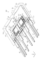
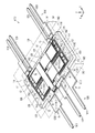
- the semiconductor device A10 of the first embodiment will be described with reference to FIGS. 1 to 3. As shown in FIGS. 1 and 2, the semiconductor device A10 includes a first die pad 11, a second die pad 12, a first switching element 20, a second switching element 30, a plurality of leads 41 to 47, and a sealing resin 70. is doing.
- the sealing resin 70 is formed so as to cover the first die pad 11 and the second die pad 12, and the first switching element 20 and the second switching element 30. Further, the sealing resin 70 is formed so as to cover a part of the plurality of leads 41 to 47.
- the sealing resin 70 is formed in a flat rectangular parallelepiped shape.
- the "rectangular parallelepiped” includes a rectangular parallelepiped in which the corners and ridges are chamfered and a rectangular parallelepiped in which the corners and ridges are rounded.
- a part or all of the constituent surfaces may be formed with irregularities or the like, or the constituent surfaces may be formed of a curved surface or a plurality of surfaces.
- the sealing resin 70 is made of a synthetic resin having electrical insulation.
- the sealing resin 70 is an epoxy resin.
- the synthetic resin constituting the sealing resin 70 is colored, for example, black.
- the sealing resin 70 is shown by a alternate long and short dash line, and the members inside the sealing resin 70 are shown by a solid line.
- the thickness direction of the sealing resin 70 is defined as the thickness direction Z, one direction orthogonal to the thickness direction Z is the lateral direction X, and the direction orthogonal to the thickness direction Z and the lateral direction X is the vertical direction. Let it be Y.
- the horizontal direction X corresponds to the first direction
- the vertical direction Y corresponds to the second direction.
- the sealing resin 70 has a resin main surface 701, a resin back surface 702, and a first resin side surface 703 to a fourth resin side surface 706.
- the resin main surface 701 and the resin back surface 702 face opposite to each other in the thickness direction Z.
- the first resin side surface 703 to the fourth resin side surface 706 face any one of the directions parallel to the resin main surface 701 and the resin back surface 702.
- the first resin side surface 703 and the second resin side surface 704 face each other in the vertical direction Y.
- the third resin side surface 705 and the fourth resin side surface 706 face each other in the lateral direction X.
- FIG. 2 is a view of the semiconductor device A10 as viewed from the side of the resin main surface 701 of the sealing resin 70.
- the shape of the sealing resin 70 is a rectangular shape in which the horizontal direction X is the long side direction and the vertical direction Y is the short side direction.
- the first resin side surface 703 and the second resin side surface 704 are side surfaces along the lateral direction X
- the third resin side surface 705 and the fourth resin side surface 706 are side surfaces along the vertical direction Y.
- the first die pad 11 and the second die pad 12 are formed in a rectangular plate shape.
- the first die pad 11 and the second die pad 12 are made of, for example, Cu (copper).
- the term "composed of Cu” means that it is made of Cu or an alloy containing Cu. It should be noted that those having a plating layer formed on a part or the whole of the surface are also included in the one made of Cu.
- the first die pad 11 has a main surface 111, a back surface 112, and a first side surface 113 to a fourth side surface 116.
- the main surface 111 and the back surface 112 face each other in the thickness direction Z.
- the main surface 111 of the first die pad 11 faces the same side as the resin main surface 701 of the sealing resin 70.
- the first side surface 113 to the fourth side surface 116 face either the horizontal direction X or the vertical direction Y.
- the first side surface 113 and the second side surface 114 face each other in the vertical direction Y, and the third side surface 115 and the fourth side surface 116 face each other in the horizontal direction X.
- the second die pad 12 has a main surface 121, a back surface 122, and a first side surface 123 to a fourth side surface 126.
- the main surface 121 and the back surface 122 face each other in the thickness direction Z.
- the main surface 121 of the second die pad 12 faces the same side as the resin main surface 701 of the sealing resin 70.
- the first side surface 123 to the fourth side surface 126 face either the horizontal direction X or the vertical direction Y.
- the first side surface 123 and the second side surface 124 face each other in the vertical direction Y
- the third side surface 125 and the fourth side surface 126 face each other in the horizontal direction X.
- the first die pad 11 and the second die pad 12 are arranged so that their main surfaces 111 and 121 are at the same position in the thickness direction Z.
- the first die pad 11 and the second die pad 12 have the same thickness.
- the thickness of the first die pad 11 and the second die pad 12 is 1 mm or more and 3 mm or less.
- the thickness of the first die pad 11 and the second die pad 12 is preferably 2 mm or more and 3 mm or less, for example.
- the back surface 112 of the first die pad 11 and the back surface 122 of the second die pad 12 are at the same position in the thickness direction Z.
- the first die pad 11 and the second die pad 12 are arranged along the lateral direction X.
- the fourth side surface 116 of the first die pad 11 and the third side surface 125 of the second die pad 12 face each other.
- the distance L12 between the first die pad 11 and the second die pad 12 is smaller than the thickness of the first die pad 11 and the second die pad 12, for example, 1 mm or more and 3 mm or less.
- the first die pad 11 and the second die pad 12 are arranged so that the first side surfaces 113 and 123 are at the same position in the vertical direction Y.
- the first switching element 20 is mounted on the main surface 111 of the first die pad 11.
- the second switching element 30 is mounted on the main surface 121 of the second die pad 12.
- the first switching element 20 and the second switching element 30 are silicon carbide (SiC) chips.
- a SiC MOSFET metal-oxide-semiconductor field-effect transistor
- the first switching element 20 and the second switching element 30 are elements capable of high-speed switching.
- the first switching element 20 is formed in a flat plate shape. Specifically, in a plan view, the shape of the first switching element 20 is, for example, a square shape. As shown in FIGS. 2 and 3, the first switching element 20 has an element main surface 201, an element back surface 202, and a first element side surface 203 to a fourth element side surface 206.
- the element main surface 201 and the element back surface 202 face in opposite directions in the thickness direction Z.
- the element main surface 201 faces the same direction as the resin main surface 701. That is, the element main surface faces the same direction as the main surface 111 of the first die pad 11.
- the element back surface 202 faces the main surface 111 of the first die pad 11.
- the side surface 203 of the first element and the side surface 204 of the second element face each other in the vertical direction Y, and the side surface 205 of the third element and the side surface 206 of the fourth element face each other in the horizontal direction X.
- the side surface 203 of the first element faces the same direction as the first side surface 113 of the first die pad 11, and the side surface 204 of the second element faces the same direction as the second side surface 114 of the first die pad 11.
- the third element side surface 205 faces the same direction as the third side surface 115 of the first die pad 11, and the fourth element side surface 206 faces the same direction as the fourth side surface 116 of the first die pad 11.
- the first switching element 20 has a first main surface electrode 21 and a first control electrode 22 on the element main surface 201, and a first back surface electrode 23 on the element back surface 202.
- the first main surface electrode 21 is a source electrode.
- the first main surface electrode 21 of the present embodiment includes a main source electrode 211 and control source electrodes 212 and 213.
- the first control electrode 22 is a gate electrode.
- the control source electrodes 212 and 213 are, for example, driver source electrodes that are electrically connected to a circuit (driver) that drives the first switching element 20.
- the first control electrode 22 is arranged at a portion closer to the side surface 205 of the third element.
- the first control electrode 22 is arranged at the center of the vertical direction Y at a portion near the side surface 205 of the third element.
- the main source electrode 211 of the first main surface electrode 21 is arranged so as to be aligned with the first control electrode 22 in the lateral direction X.
- the control source electrodes 212 and 213 are arranged so as to sandwich the first control electrode 22 in the vertical direction Y.
- the first back surface electrode 23 is a drain electrode. The first back surface electrode 23 is electrically connected to the first die pad 11 by the solder 81.
- the first switching element 20 is arranged on the main surface 111 of the first die pad 11 at a portion closer to the first side surface 113 in the vertical direction Y. Further, the first switching element 20 is arranged at the center of the first die pad 11 in the lateral direction X.
- the second switching element 30 is formed in a flat plate shape. Specifically, in a plan view, the shape of the second switching element 30 is, for example, a square shape. As shown in FIG. 2, the second switching element 30 has an element main surface 301, an element back surface 302, and a first element side surface 303 to a fourth element side surface 306.
- the element main surface 301 and the element back surface 302 face in opposite directions in the thickness direction Z.
- the element main surface 301 faces the resin main surface 701. That is, the element main surface faces the same direction as the main surface 121 of the second die pad 12.
- the element back surface 302 faces the main surface 121 of the second die pad 12.
- the side surface 303 of the first element and the side surface 304 of the second element face each other in the vertical direction Y, and the side surface 305 of the third element and the side surface 306 of the fourth element face each other in the horizontal direction X.
- the side surface 303 of the first element faces the same direction as the first side surface 123 of the second die pad 12, and the side surface 304 of the second element faces the same direction as the second side surface 124 of the second die pad 12.
- the third element side surface 305 faces the same direction as the third side surface 125 of the second die pad 12, and the fourth element side surface 306 faces the same direction as the fourth side surface 126 of the second die pad 12.
- the second switching element 30 has a second main surface electrode 31 and a second control electrode 32 on the element main surface 301, and a second back surface electrode 33 on the element back surface 302.
- the second main surface electrode 31 is a source electrode.
- the second main surface electrode 31 of the present embodiment includes a main source electrode 311 and control source electrodes 312 and 313.
- the second control electrode 32 is a gate electrode.
- the control source electrodes 312 and 313 are, for example, driver source electrodes that are electrically connected to a circuit (driver) that drives the second switching element 30.
- the second control electrode 32 is arranged at a portion near the side surface 306 of the fourth element.
- the second control electrode 32 is arranged at the center of the vertical direction Y at a portion near the side surface 306 of the fourth element.
- the main source electrode 311 of the second main surface electrode 31 is arranged so as to be aligned with the second control electrode 32 in the lateral direction X.
- the control source electrodes 312 and 313 are arranged so as to sandwich the second control electrode 32 in the vertical direction Y.
- the second back surface electrode 33 is a drain electrode. The second back surface electrode 33 is electrically connected to the second die pad 12 by the solder 82.
- the second switching element 30 is arranged on the main surface 121 of the second die pad 12 at a portion closer to the first side surface 123 in the vertical direction Y. Further, the second switching element 30 is arranged at the center of the second die pad 12 in the lateral direction X.
- the first main surface electrode 21 (main source electrode 211) of the first switching element 20 is connected to the second die pad 12 by a first wire 51 as a first connecting member.
- the first main surface electrode 21 (main source electrode 211) of the first switching element 20 and the second die pad 12 are connected by five first wires 51. ing.
- the number of the first wires 51 is set according to, for example, the drive current that can be passed through the semiconductor device A10.
- Each first wire 51 is arranged in the vertical direction Y and extends along the horizontal direction X.
- the first wires 51 are wired so as to be parallel to each other when viewed from the thickness direction Z.
- the first wire 51 is made of, for example, Al (aluminum). By being composed of Al, it is intended that it is formed of Al or an alloy containing Al.
- the first wire 51 has a circular cross-sectional shape perpendicular to the length direction near the center.
- the cross-sectional shape of the first wire 51 can be arbitrary.
- the wire diameter of the first wire 51 is, for example, 0.1 mm or more and 0.4 mm or less in the portion where the circular shape has a cross-sectional shape.
- the semiconductor device A10 includes a plurality of (7 in this embodiment) leads 41 to 47.
- the first lead 41 to the seventh lead 47 extend along the vertical direction Y.
- the first leads 41 to the seventh leads 47 project from the first resin side surface 703 of the sealing resin 70.
- the first lead 41 to the seventh lead 47 are arranged along the lateral direction X.
- the first leads 41 to the seventh leads 47 are arranged in this order from the third resin side surface 705 of the sealing resin 70 toward the fourth resin side surface 706.
- the lateral direction X is the direction in which the first die pad 11 and the second die pad 12 are arranged. Therefore, the first lead 41 to the seventh lead 47 are arranged along the arrangement direction of the first die pad 11 and the second die pad 12.
- the first lead 41 to the seventh lead 47 are made of Cu.
- the first lead 41 has a pad portion 411, a base portion 412, and a substrate connecting portion 413.
- the pad portion 411 is arranged apart from the first die pad 11 toward the first resin side surface 703 of the sealing resin 70 in the vertical direction Y.
- the pad portion 411 is a wire bonding portion to which the wire 61 is connected.
- the pad portion 411 is connected to the first control electrode 22 of the first switching element 20 by a wire 61. That is, the first lead 41 is the first control lead connected to the first control electrode (gate electrode) 22 of the first switching element 20.
- the first control lead 41 may be used instead of the first lead 41.
- the wire 61 is made of, for example, Al.
- the wire diameter of the wire 61 is, for example, 0.04 mm or more and 0.1 mm or less.
- the base portion 412 extends in the vertical direction Y from the pad portion 411 and protrudes from the first resin side surface 703 of the sealing resin 70.
- the board connection portion 413 extends in the vertical direction Y from the tip of the base portion 412.
- the board connection portion 413 is inserted into a component hole of the mounting board and is connected to the conductor wiring of the mounting board by soldering (both are not shown).
- the base portion 412 is formed to have a wider width in the lateral direction X than the substrate connecting portion 413. In the lateral direction X, the base portion 412 is formed so as to protrude from the substrate connecting portion 413 in the direction from the fourth resin side surface 706 of the sealing resin 70 toward the third resin side surface 705.
- the widths of the substrate connecting portions 413,423,433,443,453,463,473 are the same as each other.
- the width of the substrate connection portion 413 is, for example, 1.2 mm
- the width of the base portion 412 is, for example, 2.6 mm.
- the thickness of the first control lead 41 is equal to or less than the thickness of the first die pad 11.
- the thickness of the first control lead 41 is, for example, 0.6 mm.
- the second lead 42 has a pad portion 421, a base portion 422, and a substrate connecting portion 423.
- the pad portion 421 is arranged apart from the first die pad 11 toward the first resin side surface 703 of the sealing resin 70 in the vertical direction Y.
- the pad portion 421 is a wire bonding portion to which the wire 62 is connected.
- the pad portion 421 is connected to the control source electrode 312 of the first switching element 20 by a wire 62. That is, the second lead 42 is the first source lead connected to the source electrode of the first switching element 20.
- the first source lead 42 may be used instead of the second lead 42.
- the wire 62 is made of, for example, Al.
- the wire diameter of the wire 62 is, for example, 0.04 mm or more and 0.1 mm or less.
- the base portion 422 extends in the vertical direction Y from the pad portion 421 and protrudes from the first resin side surface 703 of the sealing resin 70.
- the board connection portion 423 extends in the vertical direction Y from the tip of the base portion 422.
- the board connection portion 423 is inserted into a component hole of the mounting board and is connected to the conductor wiring of the mounting board by soldering (both are not shown).
- the base portion 422 of the first source lead 42 is formed to have the same width as the substrate connection portion 423.
- the thickness of the first source lead 42 is equal to or less than the thickness of the first die pad 11, and is, for example, 0.6 mm.
- the third lead 43 has a connection portion 431, a base portion 432, and a substrate connection portion 433.
- the connection portion 431 is connected to the first die pad 11.
- the first die pad 11 is connected to the first back surface electrode (drain electrode) 23 of the first switching element 20. That is, the third lead 43 is the first drive lead (drain lead) connected to the first back surface electrode (drain electrode) 23 of the first switching element 20.
- the first drive lead 43 may be used instead of the third lead 43.
- the first drive lead 43 is integrated with the first die pad 11.
- the first drive lead 43 and the first die pad 11 constitute an integrated first lead frame 14.
- the base portion 432 extends in the vertical direction Y from the connecting portion 431 and protrudes from the first resin side surface 703 of the sealing resin 70.
- the board connection portion 433 extends in the vertical direction Y from the tip of the base portion 432.
- the board connection portion 433 is inserted into a component hole of the mounting board, and is connected to the conductor wiring of the mounting board by soldering (both are not shown).
- the base portion 432 is formed to have a wider width in the lateral direction X than the substrate connecting portion 433. In the lateral direction X, the base portion 432 is formed so as to project toward the first source lead 42 from the substrate connecting portion 433.
- the width of the substrate connection portion 433 is, for example, 1.2 mm, and the width of the base portion 432 is 2.6 mm.
- the thickness of the first drive lead 43 is equal to or less than the thickness of the first die pad 11, and is, for example, 0.6 mm.
- the fourth lead 44 has a connection portion 441, a base portion 442, and a substrate connection portion 443.
- the connection portion 441 is connected to the second die pad 12.
- the second die pad 12 is connected to the second back surface electrode (drain electrode) 33 of the second switching element 30.
- the second die pad 12 is connected to the first main surface electrode 21 (main source electrode 211) of the first switching element 20.
- the fourth lead 44 is an output lead connected to the first main surface electrode 21 (main source electrode 211) of the first switching element 20 and the second back surface electrode (drain electrode) 33 of the second switching element 30.
- the output lead 44 may be used instead of the fourth lead 44.
- the output lead 44 is integrated with the second die pad 12.
- the output lead 44 and the second die pad 12 constitute an integrated second lead frame 15.
- the base portion 442 extends in the vertical direction Y from the connecting portion 441 and protrudes from the first resin side surface 703 of the sealing resin 70.
- the substrate connection portion 443 extends in the vertical direction Y from the tip of the base portion 442.
- the base portion 442 is formed to have a wider width in the lateral direction X than the substrate connecting portion 443.
- the base portion 442 is formed so as to project toward the first drive lead 43 from the substrate connecting portion 443.
- the width of the base portion 442 and the substrate connection portion 443 of the output lead 44 and the thickness of the output lead 44 are equal to or less than the thickness of the second die pad 12, and are, for example, 0.6 mm.
- the fifth lead 45 has a pad portion 451, a base portion 452, and a substrate connecting portion 453.
- the pad portion 451 is arranged apart from the second die pad 12 toward the first resin side surface 703 of the sealing resin 70 in the vertical direction Y.
- the pad portion 451 extends along the first side surface 123 of the second die pad 12.
- the pad portion 451 is a wire bonding portion to which the second wire 52 as the second connecting member is connected.
- the pad portion 451 is connected to the second main surface electrode 31 (main source electrode 311) of the second switching element 30 by, for example, a plurality of second wires 52.
- FIG. 2 shows five second wires 52. Each second wire 52 is arranged in the lateral direction X.
- the second wires 52 are wired so as to be parallel to each other when viewed from the thickness direction Z. That is, the fifth lead 45 is a second drive lead (source lead) connected to the second main surface electrode 31 (main source electrode 311) of the second switching element 30. In the following description, the second drive lead 45 may be used instead of the fifth lead 45.
- the second wire 52 is made of, for example, Al.
- the wire diameter of the second wire 52 is, for example, 0.1 mm or more and 0.4 mm or less.
- the base portion 452 extends in the vertical direction Y from the pad portion 451 and protrudes from the first resin side surface 703 of the sealing resin 70.
- the substrate connecting portion 453 extends in the vertical direction Y from the tip of the base portion 452.
- the base portion 452 is formed to have a wider width in the lateral direction X than the substrate connecting portion 453. In the lateral direction X, the base portion 452 is formed so as to project toward the sixth lead 46 from the substrate connecting portion 453.
- the width of the base portion 452 and the substrate connecting portion 453 of the second drive lead 45 and the thickness of the second drive lead 45 are equal to or less than the thickness of the second die pad 12, and are, for example, 0.6 mm.
- the sixth lead 46 has a pad portion 461, a base portion 462, and a substrate connecting portion 463.
- the pad portion 461 is arranged apart from the second die pad 12 toward the first resin side surface 703 of the sealing resin 70 in the vertical direction Y.
- the pad portion 461 is a wire bonding portion to which the wire 63 is connected.
- the pad portion 461 is connected to the control source electrode 313 of the second switching element 30 by, for example, one wire 63. That is, the sixth lead 46 is a source lead connected to the control source electrode 313 of the second switching element 30.
- the second source lead 46 may be used instead of the sixth lead 46.
- the wire 63 is made of, for example, Al.
- the wire diameter of the wire 63 is, for example, 0.04 mm or more and 0.1 mm or less.
- the base portion 462 extends in the vertical direction Y from the pad portion 461 and protrudes from the first resin side surface 703 of the sealing resin 70.
- the substrate connection portion 463 extends in the vertical direction Y from the tip of the base portion 462.
- the base portion 462 of the second source lead 46 is formed to have the same width as the substrate connecting portion 463.
- the width of the base portion 462 and the substrate connecting portion 463 of the second source lead 46 and the thickness of the second source lead 46 are equal to or less than the thickness of the second die pad 12, and are, for example, 0.6 mm.
- the seventh lead 47 has a pad portion 471, a base portion 472, and a substrate connecting portion 473.
- the pad portion 471 is arranged apart from the second die pad 12 toward the first resin side surface 703 of the sealing resin 70 in the vertical direction Y.
- the pad portion 471 is a wire bonding portion to which the wire 64 is connected.
- the pad portion 471 is connected to the second control electrode 32 of the second switching element 30 by a wire 64. That is, the seventh lead 47 is a second control lead connected to the second control electrode (gate electrode) 32 of the second switching element 30. In the following description, the second control lead 47 may be used instead of the seventh lead 47.
- the wire 64 is made of, for example, Al.
- the wire diameter of the wire 64 is, for example, 0.04 mm or more and 0.1 mm or less.
- the base portion 472 extends in the vertical direction Y from the pad portion 471 and protrudes from the first resin side surface 703 of the sealing resin 70.
- the board connection portion 473 extends in the vertical direction Y from the selection of the base portion 472.
- the base portion 472 is formed to have a wider width in the lateral direction X than the substrate connecting portion 473.
- the base portion 472 is formed so as to protrude from the substrate connecting portion 473 in the direction from the third resin side surface 705 of the sealing resin 70 toward the fourth resin side surface 706.
- the width of the base portion 472 and the substrate connecting portion 473 of the second control lead 47 and the thickness of the second control lead 47 are equal to or less than the thickness of the second die pad 12, and are, for example, 0.6 mm.
- the thicknesses of the first leads 41 to the seventh leads 47 are equal to each other.
- the distance between the first control lead 41 and the first source lead 42 and the distance between the second source lead 46 and the second control lead 47 are compared with each other in the first source lead 42 to the second source lead 46.
- the leads 41 to 47 are arranged so that the distance between the two leads adjacent to each other in the direction X is wide.
- the first source lead 42 to the second source lead 46 are arranged so that the intervals between the bases 422, 432, 442, 452, 462 are equal.
- the sealing resin 70 has recesses 707 extending from the side surface 703 of the first resin along the vertical direction Y between the first source lead 42 and the second source lead 46.
- FIG. 4 shows a comparative example with respect to the present embodiment.
- an inverter circuit or the like is configured by using two semiconductor devices 90a and 90b.
- the semiconductor devices 90a and 90b are electrically connected to one switching element 91, the gate electrode 911 of the switching element 91, the control source electrode 912, the main source electrode 913, and the back surface electrode (drain electrode) 914, respectively. It has leads 921 to 924.
- Each of the electrodes 911 to 914 is connected to leads 921 to 924, respectively.
- the inverter circuit is configured by electrically connecting the back electrode (drain electrode) 914 of the switching element 91 of one semiconductor device 90a and the main source electrode 913 of the switching element 91 of the other semiconductor device 90b by an external wiring OP.
- the external wiring OP is, for example, a conductor wiring of a mounting board on which semiconductor devices 90a and 90b are mounted. In FIG. 4, the tips of the leads 924 and 923 are shown to be connected by the external wiring OP.
- the lead 923 of one semiconductor device 90b is connected to the conductor wiring that supplies a low potential voltage
- the lead 924 of the other semiconductor device 90a is connected to the conductor wiring that supplies a high potential voltage.
- Two semiconductor devices 90a and 90b and an external wiring OP are interposed between the lead 923 and the lead 924. Due to the parasitic inductance of the external wiring OP, the inductances in the lead 924 (drain lead), the lead 923 (output lead), and the lead 923 (source lead) become large.
- the semiconductor device A10 of the present embodiment includes a first switching element 20 and a second switching element 30 in one sealing resin 70.
- the first main surface electrode 21 (main source electrode 211) of the first switching element 20 is connected to the second die pad 12 on which the second switching element 30 is mounted by the first wire 51 as the first connecting member. Therefore, in the semiconductor device A10 of the present embodiment, the conductor distance between the first drive lead 43 (first drive lead), the output lead 44 (output lead), and the second drive lead 45 (second drive lead) is shortened.
- the inductance of the semiconductor device A10 is smaller than that of the above comparative example, and is approximately 1 ⁇ 2. As described above, in the semiconductor device A10 of the present embodiment, the inductance can be reduced.
- the semiconductor device A10 includes a first switching element 20 and a second switching element 30 in one sealing resin 70.
- the first main surface electrode 21 (main source electrode 211) of the first switching element 20 is connected to the second die pad 12 on which the second switching element 30 is mounted by the first wire 51 as the first connecting member. Therefore, in the semiconductor device A10, the conductor distance between the first drive lead 43 (first drive lead), the output lead 44 (output lead), and the second drive lead 45 (second drive lead) is shortened, and the inductance is reduced. can.
- the thickness of the first die pad 11 and the second die pad 12 is 1 mm or more and 3 mm or less. It is preferable that the first die pad 11 and the second die pad are thick.
- the heat generated by the operation of the first switching element 20 is transferred from the first switching element 20 to the first die pad 11.
- the thermal resistance in the second switching element 30 can be reduced.
- the plurality of first wires 51 as the first connecting member are wired so as to be parallel to each other when viewed from the thickness direction Z. Therefore, in the step of connecting the plurality of first wires 51, the plurality of first wires 51 can be connected by the same operation without changing the angle of the wire or the loop height of the wire, and the manufacturing becomes easy.
- the main source electrode 311 of the second switching element 30 is connected to the pad portion 451 of the second drive lead 45 by a plurality of second wires 52.
- the second wires 52 are wired so as to be parallel to each other when viewed from the thickness direction Z. Therefore, in the step of connecting the plurality of second wires 52, the plurality of wires 62 can be connected by the same operation without changing the angle of the wires or the loop height of the wires, which facilitates manufacturing.
- the first source lead 42 to the second source lead 46 are lateral.
- the leads 41 to 47 are arranged so that the distance between the two leads adjacent to each other in the direction X is wide.
- the first source lead 42 to the second source lead 46 are arranged so that the intervals of the bases 422, 432, 442, 452, 462 of the first source lead 42 to the second source lead 46 are equal to each other. ing. Therefore, in the first source lead 42 to the second source lead 46, the distance between adjacent leads becomes long, and insulation can be ensured.
- the sealing resin 70 has recesses 707 extending along the vertical direction Y from the side surface 703 of the first resin between the first source lead 42 and the second source lead 46.
- the recess 707 increases the distance (creeping distance) along the surface of the sealing resin 70 between the first source lead 42 and the first drive lead 43, so that the first source lead 42 and the first drive lead 43 are separated from each other. Insulation between can be secured.
- the creepage distance between the leads 43, 44, the leads 44, 45, and the leads 45, 46 sandwiching each recess 707 becomes long, and insulation can be ensured.
- the first embodiment can be modified and implemented as follows.
- the configurations of the first switching element 20 and the second switching element 30 may be appropriately changed.
- the first switching element 20 the first main surface electrode 21 is divided into the main source electrode 211 and the control source electrodes 212 and 213, but a switching element that is not divided is used as the first main surface electrode. You may.
- the first wire 51 and the wire 62 shown in FIGS. 1 and 2 are connected to one first main surface electrode.
- the second main surface electrode 31 including the main source electrode 311 and the control source electrodes 312 and 313 is used, but the switching element which is not divided is used as the second main surface electrode. May be good.
- the second wire 52 and the wire 63 shown in FIGS. 1 and 2 are connected to one first main surface electrode.
- each lead may be changed as appropriate.
- the semiconductor device A11 shown in FIG. 5 includes first leads 41 to seventh leads 47 having the same thickness as each other.
- the thickness of the third reed 43 to the fifth reed is equal to the thickness of the first die pad 11 and the second die pad 12.
- the thickness of the first lead 41, the second lead 42, the sixth lead 46, and the seventh lead 47 is the same as the thickness of the third lead 43 to the fifth lead 45, but the first lead.
- Either one of 41 and the second lead 42, and one of the sixth lead 46 and the seventh lead 47 may have a thickness different from that of the third lead 43 to the fifth lead 45.
- at least one of the third lead 43 to the fifth lead 45 may be different from the thickness of the first die pad 11 and the second die pad 12.
- the number of the first wire 51 as the first connecting member connecting the first switching element 20 and the second die pad 12 may be 4 or less, or 6 or more.
- the number of the second wire 52 as the second connecting member connecting the second switching element 30 and the fifth lead 45 may be 4 or less, or 6 or more.
- the semiconductor device A20 of the second embodiment is different from the semiconductor device A10 of the first embodiment described above in that the connection between the fourth lead and the fifth lead is mainly different.
- the same reference numerals may be given to the configurations common to the configurations of the semiconductor device A10 of the first embodiment, and the description thereof may be omitted.
- the semiconductor device A20 of the present embodiment includes a plurality of leads 41, 42, 43, 44a, 45a, 46, 47 protruding from the first resin side surface 703 of the sealing resin 70. ing.
- the fourth lead 44a has a pad portion 444, a base portion 442, and a substrate connecting portion 443.
- the pad portion 444 is arranged apart from the second die pad 12 toward the first resin side surface 703 of the sealing resin 70 in the vertical direction Y.
- the pad portion 444 extends along the first side surface 123 of the second die pad 12.
- the pad portion 444 is a wire bonding portion to which the second wire 52 as the second connecting member is connected.
- the pad portion 444 is connected to the second main surface electrode 31 (main source electrode 311) of the second switching element 30 by, for example, a plurality of second wires 52. 6 and 7 show five second wires 52. That is, the fourth lead 44a is a second drive lead (source lead) connected to the second main surface electrode 31 (main source electrode 311) of the second switching element 30.
- the fifth lead 45a has a connection portion 454, a base portion 452, and a substrate connection portion 453.
- the connection portion 454 is connected to the second die pad 12.
- the second die pad 12 is connected to the second back surface electrode 33 (drain electrode) of the second switching element 30. Further, the second die pad 12 is connected to the first main surface electrode 21 (main source electrode 211) of the first switching element 20. That is, the fifth lead 45a is an output lead connected to the first main surface electrode 21 (main source electrode 211) of the first switching element 20 and the second back surface electrode 33 (drain electrode) of the second switching element 30. be.
- the fifth lead 45a is integrated with the second die pad 12.
- the fifth lead 45a and the second die pad 12 constitute an integrated second lead frame 15a.
- the semiconductor device A20 of the present embodiment is arranged in the order of the first drive lead 43 (third lead), the second drive lead 44a (fourth lead), and the output lead 45a (fifth lead) in the lateral direction X. There is. That is, the first drive lead 43 and the second drive lead 44a are arranged side by side. A high potential voltage is supplied to the first drive lead 43, and a low potential voltage is supplied to the second drive lead 44a.
- FIG. 9 shows the current when the semiconductor device A20 of this embodiment is operated.
- the first switching element 20 is turned on and the second switching element 30 is turned off
- the first current I1 flows from the first drive lead 43 toward the output lead 45a.
- the second current I2 flows from the output lead 45a toward the second drive lead 44a.
- the semiconductor device A20 is operated with a high-speed control signal (for example, 1 MHz)
- the first current I1 and the second current I1 and the second current in the opposite directions to the semiconductor device A20 are used in the adjacent first drive lead 43 and second drive lead 44a.
- the current I2 and the current I2 flow alternately.
- the magnetic flux generated by the first current I1 and the second current I2 lowers the mutual inductance, so that the parasitic inductance in the semiconductor device A20 is further lowered.
- the semiconductor device A20 is arranged in the order of the first drive lead 43 (third lead), the second drive lead 44a (fourth lead), and the output lead 45a (fifth lead) in the lateral direction X. ing.
- the inductance in the semiconductor device A20 can be further reduced by the first current I1 flowing from the first drive lead 43 toward the output lead 45a and the second current I2 flowing from the output lead 45a toward the second drive lead 44a.
- the semiconductor device A30 of the third embodiment will be described with reference to FIGS. 10 to 14.
- the semiconductor device A30 of the third embodiment is different from the semiconductor device A10 of the first embodiment described above in that the first connecting member and the second connecting member are different.
- the same reference numerals may be given to the configurations common to the configurations of the semiconductor device A10 of the first embodiment, and the description thereof may be omitted.
- the semiconductor device A30 of the present embodiment includes a first clip 53 as a first connecting member. Further, the semiconductor device A30 of the present embodiment includes a second clip 54 as a second connecting member.
- the first switching element 20 is connected to the second die pad 12 by the first clip 53.
- the first clip 53 is a plate-shaped member having conductivity.
- the first clip 53 is formed by bending a plate-shaped conductive plate.
- the first clip 53 of the present embodiment has a strip shape extending in the lateral direction X.
- the first clip 53 connects the first main surface electrode 21 (main source electrode 211) of the first switching element 20 and the second die pad 12. As shown in FIG. 13, one end of the first clip 53 is connected to the main source electrode 211 of the first switching element 20 by the solder 83, and the other end of the first clip 53 is connected to the second die pad 12 by the solder 84. Has been done.
- the first clip 53 is made of Cu.
- the thickness of the first clip 53 is 0.05 mm or more and 1.0 mm or less, preferably 0.5 mm or more.
- the second switching element 30 is connected to the fifth lead 45 (second drive lead) by the second clip 54.
- the second clip 54 is a plate-shaped member having conductivity.
- the second clip 54 is formed by bending a plate-shaped conductive plate.
- the second clip 54 of the present embodiment has a strip shape extending in the vertical direction Y.
- the second clip 54 connects the second main surface electrode 31 (main source electrode 311) of the second switching element 30 and the pad portion 451 of the fifth lead 45.
- one end of the second clip 54 is connected to the main source electrode 311 of the second switching element 30 by the solder 85, and the other end of the second clip 54 is connected to the pad of the fifth lead 45 by the solder 86. It is connected to the unit 451.
- the second clip 54 is made of Cu.
- the thickness of the second clip 54 is 0.05 mm or more and 1.0 mm or less, preferably 0.5 mm or more.
- the first switching element 20 and the second die pad 12 were connected by the first clip 53. Therefore, it is possible to cope with a large current as compared with the case where the first switching element 20 and the second die pad 12 are connected by a plurality of wires.
- the semiconductor device A40 of the fourth embodiment will be described with reference to FIGS. 15 to 18.
- the semiconductor device A40 of the fourth embodiment is different from the semiconductor device A30 of the third embodiment described above in that the connection between the fourth lead and the fifth lead is mainly different.
- the same reference numerals may be given to the configurations common to the configurations of the semiconductor device A30 of the third embodiment, and the description thereof may be omitted.
- the semiconductor device A40 of the present embodiment includes a plurality of leads 41, 42, 43, 44a, 45a, 46, 47 protruding from the first resin side surface 703 of the sealing resin 70. ing.
- the fourth lead 44a has a pad portion 444, a base portion 442, and a substrate connecting portion 443.
- the pad portion 444 is arranged apart from the second die pad 12 toward the first resin side surface 703 of the sealing resin 70 in the vertical direction Y.
- the pad portion 444 extends along the first side surface 123 of the second die pad 12.
- the pad portion 444 is connected to the second main surface electrode 31 (main source electrode 311) of the second switching element 30 by the second clip 54a as the second connecting member.
- the fourth lead 44a is a second drive lead (source lead) connected to the second main surface electrode 31 (main source electrode 311) of the second switching element 30.
- the second clip 54a is a plate-shaped member having conductivity.
- the second clip 54a is formed by bending a plate-shaped conductive plate.
- the second clip 54a has a lead connecting portion 541, an electrode connecting portion 542, and a connecting portion 543.
- the lead connection portion 541 extends in the lateral direction X in the same manner as the pad portion 444 of the fourth lead 44a, and is connected to the pad portion 444 by the solder 86.
- the electrode connecting portion 542 is formed in a rectangular shape corresponding to the second main surface electrode 31 (main source electrode 311) of the second switching element 30, and is connected to the second main surface electrode 31 by the solder 85.
- the connecting portion 543 connects the lead connecting portion 541 and the electrode connecting portion 542.
- the connecting portion 543 extends in the vertical direction Y from the lead connecting portion 541.
- the connecting portion 543 is connected to the end portion of the electrode connecting portion 542 near the first die pad 11. That is, the electrode connecting portion 542 extends in the lateral direction X from the connecting portion 543.
- the second clip 54a connects the connecting portion 543 between the second switching element 30 and the third side surface 125 of the second die pad 12 to the main surface 121 of the second die pad 12. It is formed so as to be parallel to.
- the fifth lead 45a has a connection portion 454, a base portion 452, and a substrate connection portion 453.
- the connection portion 454 is connected to the second die pad 12.
- the second die pad 12 is connected to the second back surface electrode 33 (drain electrode) of the second switching element 30. Further, the second die pad 12 is connected to the first main surface electrode 21 (main source electrode 211) of the first switching element 20. That is, the fifth lead 45a is an output lead connected to the first main surface electrode 21 (main source electrode 211) of the first switching element 20 and the second back surface electrode 33 (drain electrode) of the second switching element 30. be.
- the fifth lead 45a is integrated with the second die pad 12.
- the fifth lead 45a and the second die pad 12 constitute an integrated second lead frame 15a.
- a semiconductor is provided by a first current I1 (see FIG. 9) flowing from the first drive lead 43 toward the output lead 45a and a second current I2 (see FIG. 9) flowing from the output lead 45a toward the second drive lead 44a.
- the inductance in the device A40 can be reduced.
- the second clip 54a connecting the second switching element 30 and the second drive lead 44a has a lead connecting portion 541 connected to the fourth lead 44a and an electrode connected to the second switching element 30. It has a connecting portion 542 and a connecting portion 543 that connects the lead connecting portion 541 and the electrode connecting portion 542.
- the connecting portion 543 is arranged so as to be parallel to the second die pad 12. Therefore, there are many adjacent portions between the first drive lead 43 (third lead) and the output lead 45a (fifth lead), and between the output lead 45a and the second drive lead 44a (fourth lead). , Inductance can be further reduced.
- the semiconductor device A50 of the fifth embodiment will be described with reference to FIGS. 19 to 21.
- the semiconductor device A50 of the fifth embodiment has a different position of the switching element from the semiconductor device A40 of the fourth embodiment described above.
- the same reference numerals may be given to the configurations common to the configurations of the semiconductor device A40 of the fourth embodiment, and the description thereof may be omitted.
- the first switching element 20 and the second switching element 30 are arranged near the center of the sealing resin 70.
- the arrangement of the first switching element 20 and the second switching element 30 will be described in detail.
- the first switching element 20 is arranged on the main surface 111 of the first die pad 11 in the vertical direction Y closer to the first side surface 113. As shown in FIGS. 20 and 21, the first switching element 20 is arranged closer to the fourth side surface 116 of the first die pad 11 in the lateral direction X. The fourth side surface 116 faces the third side surface 125 of the second die pad 12. That is, the first switching element 20 is arranged closer to the second die pad 12 in the first die pad 11. As a result, the length of the first clip 53 connecting the first switching element 20 and the second die pad 12 can be shortened.
- the distance (first distance) Lx1 from the fourth side surface 116 of the first die pad 11 to the fourth element side surface 206 of the first switching element 20 when viewed from the thickness direction Z is the distance (first distance) Lx1 of the first die pad 11. It is thicker than the thickness.
- the second switching element 30 is arranged on the main surface 121 of the second die pad 12 near the first side surface 123 in the vertical direction Y. As shown in FIGS. 20 and 21, the second switching element 30 is arranged closer to the third side surface 125 of the second die pad 12 in the lateral direction X. That is, the second switching element 30 is arranged closer to the first die pad 11 in the second die pad 12. As a result, the length of the electrical path from the first switching element 20 to the second switching element 30 can be shortened.
- the distance (second distance) Lx2 from the third side surface 125 of the second die pad 12 to the third element side surface 305 of the second switching element 30 when viewed from the thickness direction Z is the distance (second distance) Lx2 of the second die pad 12. It is thicker than the thickness.
- the first switching element 20 is arranged near the fourth side surface 116 of the first die pad 11 in the lateral direction X.
- the second switching element 30 is arranged closer to the third side surface 125 of the second die pad 12 in the lateral direction X.
- the heat generated by the operation of the first switching element 20 is transferred from the first switching element 20 to the first die pad 11.
- heat is transferred while diffusing from the main surface 111 of the first die pad 11 toward the back surface 112, as shown by an arrow in FIG. 21.
- heat is transferred from each surface of the first die pad 11 to the sealing resin 70.
- the heat generated by the operation of the second switching element 30 is transferred from the second switching element 30 to the second die pad 12, and is transmitted while diffusing from the main surface 121 of the second die pad 12 toward the back surface 122. Then, heat is transferred from each surface of the second die pad 12 to the sealing resin 70.
- the heat transfer efficiency from 125 to the resin portion 70a is reduced. That is, the heat dissipation efficiency for the first switching element 20 and the second switching element 30 is lowered.
- the distance Lx1 from the fourth side surface 116 of the first die pad 11 to the fourth element side surface 206 of the first switching element 20 is the thickness of the first die pad 11. That is all.
- the distance Lx2 from the third side surface 125 of the second die pad 12 to the third element side surface 305 of the second switching element 30 is equal to or larger than the thickness of the second die pad 12.
- the first switching element 20 is arranged closer to the second die pad 12 in the first die pad 11, and the second switching element 30 is arranged closer to the first die pad 11 in the second die pad 12. .. Therefore, the length of the electric path from the first switching element 20 to the second switching element 30 can be shortened, and the parasitic inductance in the electric path between the elements can be made smaller.
- the distance Lx1 from the fourth side surface 116 of the first die pad 11 to the fourth element side surface 206 of the first switching element 20 is equal to or larger than the thickness of the first die pad 11. As a result, it is possible to suppress a decrease in heat dissipation efficiency of the first die pad 11 with respect to the first switching element 20.
- the distance Lx2 from the third side surface 125 of the second die pad 12 to the third element side surface 305 of the second switching element 30 is equal to or larger than the thickness of the second die pad 12. As a result, it is possible to suppress a decrease in heat dissipation efficiency of the second die pad 12 with respect to the second switching element 30.
- the semiconductor device A61 is mounted on the first die pad 11 and connected in parallel to the two first switching elements 20, and mounted on the second die pad 12 and connected in parallel to each other. It includes two second switching elements 30.
- the amount of current flowing through the semiconductor device A61 can be increased.
- Three or more first switching elements 20 may be mounted on the first die pad 11, and three or more second switching elements 30 may be mounted on the second die pad 12. The number of switching elements to be mounted is determined according to the amount of current flowing through the semiconductor device A61.
- each member constituting the semiconductor device may be changed as appropriate.
- 23 to 26 show an example of changing the shapes of the lead and the second connecting member.
- the width of the base 442 of the fourth lead 44a is made wider than the width of the base 432 of the third lead 43 and the base 452 of the fifth lead 45a. May be good.
- each base 432,442,452 may be wider than the width of the base 412 of the first lead 41 and the base 472 of the seventh lead 47.
- the width of the second clip 54a may be widened as in the semiconductor device A64 shown in FIG. Further, as in the semiconductor device A65 shown in FIG. 26, by using the first switching element 20 and the second switching element 30 as, for example, a Si element, the base 442 of the fourth lead 44a can be replaced with the base 432 of the third lead 43. It can be brought closer to the base 452 of the fifth lead 45a to reduce the inductance.
- the semiconductor device A70 of the sixth embodiment will be described with reference to FIGS. 27 to 31.
- the semiconductor device A70 includes a first die pad 11, a second die pad 12, a first lead group 1020 (leads 1021 to 1023), a second lead group 1030 (leads 1031 to 1034), and a first. It has one switching element 40a, 40b, a second switching element 50a, 50b, a first connecting member 1061, a second connecting member 1062, wires 71 to 76, and a sealing resin 900.
- the sealing resin 900 covers the first die pad 11, the second die pad 12, the first switching elements 40a and 40b and the second switching elements 50a and 50b, the first connecting member 1061, the second connecting member 1062, and the wires 71 to 76. It is formed like this. Further, the sealing resin 900 is formed so as to cover a part of the first lead group 1020 (leads 1021 to 1023) and the second lead group 1030 (leads 1031 to 1034).
- the sealing resin 900 is formed in a flat rectangular parallelepiped shape.
- the "rectangular parallelepiped” includes a rectangular parallelepiped in which the corners and ridges are chamfered and a rectangular parallelepiped in which the corners and ridges are rounded.
- a part or all of the constituent surfaces may be formed with irregularities or the like, or the constituent surfaces may be formed of a curved surface or a plurality of surfaces.
- the sealing resin 900 is made of a synthetic resin having electrical insulation.
- the sealing resin 900 is an epoxy resin.
- the synthetic resin constituting the sealing resin 900 is colored, for example, black.
- the sealing resin 900 is shown by a alternate long and short dash line, and the members inside the sealing resin 900 are shown by a solid line.
- the thickness direction of the sealing resin 900 is defined as the thickness direction Z, one direction orthogonal to the thickness direction Z is the lateral direction X, and the direction orthogonal to the thickness direction Z and the lateral direction X is the vertical direction. Let it be Y.
- the horizontal direction X corresponds to the first direction
- the vertical direction Y corresponds to the second direction.
- the sealing resin 900 has a resin main surface 901, a resin back surface 902, and a first resin side surface 903 to a fourth resin side surface 906.
- the resin main surface 901 and the resin back surface 902 face opposite to each other in the thickness direction Z.
- the first resin side surface 903 to the fourth resin side surface 906 face any one of the directions parallel to the resin main surface 901 and the resin back surface 902.
- the first resin side surface 903 and the second resin side surface 904 face opposite to each other in the vertical direction Y.
- the third resin side surface 905 and the fourth resin side surface 906 face each other in the lateral direction X.
- FIG. 28 is a view of the semiconductor device A70 from the side of the resin main surface 901 of the sealing resin 900.
- the shape of the sealing resin 900 is a rectangular shape in which the horizontal direction X is the long side direction and the vertical direction Y is the short side direction.
- the first resin side surface 903 and the second resin side surface 904 are side surfaces along the lateral direction X
- the third resin side surface 905 and the fourth resin side surface 906 are side surfaces along the vertical direction Y.
- the first die pad 11 and the second die pad 12 are formed in a rectangular plate shape.
- the first die pad 11 and the second die pad 12 are made of, for example, Cu (copper).
- the term "composed of Cu” means that it is made of Cu or an alloy containing Cu. It should be noted that those having a plating layer formed on a part or the whole of the surface are also included in the one made of Cu.
- the first die pad 11 has a main surface 111, a back surface 112, and a first side surface 113 to a fourth side surface 116.
- the main surface 111 and the back surface 112 face each other in the thickness direction Z.
- the main surface 111 of the first die pad 11 faces the same side as the resin main surface 901 of the sealing resin 900.
- the first side surface 113 to the fourth side surface 116 face either the horizontal direction X or the vertical direction Y.
- the first side surface 113 and the second side surface 114 face each other in the vertical direction Y
- the third side surface 115 and the fourth side surface 116 face each other in the horizontal direction X.
- the second die pad 12 has a main surface 121, a back surface 122, and a first side surface 123 to a fourth side surface 126.
- the main surface 121 and the back surface 122 face each other in the thickness direction Z.
- the main surface 121 of the second die pad 12 faces the same side as the resin main surface 901 of the sealing resin 900.
- the first side surface 123 to the fourth side surface 126 face either the horizontal direction X or the vertical direction Y.
- the first side surface 123 and the second side surface 124 face each other in the vertical direction Y
- the third side surface 125 and the fourth side surface 126 face each other in the horizontal direction X.
- the first die pad 11 and the second die pad 12 are arranged so that their main surfaces 111 and 121 are at the same position in the thickness direction Z.
- the first die pad 11 and the second die pad 12 have the same thickness.
- the thickness of the first die pad 11 and the second die pad 12 is 1 mm or more and 3 mm or less.
- the thickness of the first die pad 11 and the second die pad 12 is preferably 2 mm or more and 3 mm or less, for example.
- the back surface 112 of the first die pad 11 and the back surface 122 of the second die pad 12 are at the same position in the thickness direction Z.
- the first die pad 11 and the second die pad 12 are arranged along the lateral direction X.
- the fourth side surface 116 of the first die pad 11 and the third side surface 125 of the second die pad 12 face each other.
- the distance L12 between the first die pad 11 and the second die pad 12 is smaller than the thickness of the first die pad 11 and the second die pad 12, for example, 1 mm or more and 3 mm or less.
- the first die pad 11 and the second die pad 12 are arranged so that the first side surfaces 113 and 123 are at the same position in the vertical direction Y.
- the semiconductor device A70 has a first lead group 1020 and a second lead group 1030.
- the first lead group 1020 is composed of a plurality of (three in this embodiment) leads 1021 to 1023 protruding from the first resin side surface 903 of the sealing resin 900.
- the second lead group 1030 is composed of a plurality of (four in this embodiment) leads 1031 to 1034 from the second resin side surface 904 of the sealing resin 900.
- the leads 1021 to 1023 of the first lead group 1020 are arranged along the horizontal direction X and extend along the vertical direction Y.
- the leads 1031 to 1034 of the second lead group 1030 are arranged along the horizontal direction X and extend along the vertical direction Y. Leads 1021 to 1023 and 1031 to 1034 are made of Cu.
- the first lead group 1020 is composed of a first drive lead 1021, a second drive lead 1022, and an output lead 1023.
- the first drive lead 1021 is arranged at the center of the first die pad 11 in the lateral direction X.
- the first drive lead 1021 has a connection portion 1211, a base portion 1212, and a substrate connection portion 1213.
- the connecting portion 1211 is connected to the first side surface 113 of the first die pad 11.
- the first drive lead 1021 is integrated with the first die pad 11.
- the first drive lead 1021 and the first die pad 11 constitute an integrated first lead frame 14.
- the base portion 1212 extends in the vertical direction Y from the connecting portion 1211 and protrudes from the first resin side surface 903 of the sealing resin 900.
- the substrate connection portion 1213 extends in the vertical direction Y from the tip of the base portion 1212.
- the board connection portion 1213 is inserted into a component hole of the mounting board and is connected to the conductor wiring of the mounting board by soldering (both are not shown).
- the base portion 1212 is formed to have a wider width in the lateral direction X than the substrate connecting portion 1213. In the lateral direction X, the base portion 1212 is formed so as to protrude from the substrate connecting portion 1213 in the direction from the fourth resin side surface 906 of the sealing resin 900 toward the third resin side surface 905.
- the second drive lead 1022 is arranged at the center of the sealing resin 900 in the lateral direction X.
- the second drive lead 1022 has a pad portion 1221, a base portion 1222, and a substrate connecting portion 1223.
- the pad portion 1221 is arranged apart from the second die pad 12 toward the first resin side surface 903 of the sealing resin 900 in the vertical direction Y.
- the pad portion 1221 extends along the first side surface 113 of the first die pad 11 and the first side surface 123 of the second die pad 12. That is, the pad portion 1221 is arranged so as to straddle the first side surface 123 of the second die pad 12 from the first side surface 113 of the first die pad 11.
- the pad portion 1221 is a connecting portion to which the second connecting member 1062 is connected.
- the base portion 1222 extends in the vertical direction Y from the pad portion 1221 and protrudes from the first resin side surface 903 of the sealing resin 900.
- the substrate connection portion 1223 extends in the vertical direction Y from the tip of the base portion 1222.
- the base portion 1222 is formed to have a wider width in the lateral direction X than the substrate connecting portion 1223.
- the base portion 1222 is formed so as to protrude from the substrate connecting portion 1223 in the direction from the third resin side surface 905 to the fourth resin side surface 906 of the sealing resin 900.
- the output lead 1023 is arranged at the center of the second die pad 12 in the lateral direction X.
- the output lead 1023 has a connection portion 1231, a base portion 1232, and a substrate connection portion 1233.
- the connecting portion 1231 is connected to the first side surface 123 of the second die pad 12.
- the output lead 1023 is integrated with the second die pad 12.
- the output lead 1023 and the second die pad 12 constitute an integrated second lead frame 15.
- the base portion 1232 extends in the vertical direction Y from the connecting portion 1231 and protrudes from the first resin side surface 903 of the sealing resin 900.
- the substrate connection portion 1233 extends in the vertical direction Y from the tip of the base portion 1232. As shown in FIG.
- the base portion 1232 is formed to have a wider width in the lateral direction X than the substrate connecting portion 1233. In the lateral direction X, the base portion 1232 is formed so as to protrude from the substrate connecting portion 1233 in the direction from the third resin side surface 905 to the fourth resin side surface 906 of the sealing resin 900.
- the second read group 1030 is composed of a first control lead 1031, a first source lead 1032, a second source lead 1033, and a second control lead 1034.
- the first control lead 1031 has a pad portion 1311, a base portion 1312, and a substrate connecting portion 1313.
- the pad portion 1311 is arranged apart from the first die pad 11 toward the second resin side surface 904 of the sealing resin 900 in the vertical direction Y.
- the pad portion 1311 is a wire bonding portion to which the wires 71 and 72 are connected.
- the base portion 1312 extends in the vertical direction Y from the pad portion 1311 and protrudes from the second resin side surface 904 of the sealing resin 900.
- the substrate connection portion 1313 extends in the vertical direction Y from the tip of the base portion 1312.
- the base portion 1312 is formed to have a wider width in the lateral direction X than the substrate connecting portion 1313. In the lateral direction X, the base portion 1312 is formed so as to protrude from the substrate connecting portion 1313 in the direction from the fourth resin side surface 906 to the third resin side surface 905.
- the first source lead 1032 has a pad portion 1321, a base portion 1322, and a substrate connection portion 1323.
- the pad portion 1321 is arranged apart from the first die pad 11 toward the second resin side surface 904 of the sealing resin 900 in the vertical direction Y.
- the pad portion 1321 is a wire bonding portion to which the wire 73 is connected.
- the base portion 1322 extends in the vertical direction Y from the pad portion 1321 and protrudes from the second resin side surface 904 of the sealing resin 900.
- the substrate connection portion 1323 extends in the vertical direction Y from the tip of the base portion 1322.
- the second source lead 1033 has a pad portion 1331, a base portion 1332, and a substrate connection portion 1333.
- the pad portion 1331 is arranged apart from the second die pad 12 toward the second resin side surface 904 of the sealing resin 900 in the vertical direction Y.
- the pad portion 1331 is a wire bonding portion to which the wire 76 is connected.
- the base portion 1332 extends in the vertical direction Y from the pad portion 1331 and protrudes from the second resin side surface 904 of the sealing resin 900.
- the substrate connection portion 1333 extends in the vertical direction Y from the tip of the base portion 1332.
- the second control lead 1034 has a pad portion 1341, a base portion 1342, and a substrate connection portion 1343.
- the pad portion 1341 is arranged apart from the second die pad 12 toward the second resin side surface 904 of the sealing resin 900 in the vertical direction Y.
- the pad portion 1341 is a wire bonding portion to which the wires 74 and 75 are connected.
- the base portion 1342 extends in the vertical direction Y from the pad portion 1341 and protrudes from the second resin side surface 904 of the sealing resin 900.
- the board connection portion 1343 extends in the vertical direction Y from the selection of the base portion 1342.
- the base portion 1342 is formed to have a wider width in the lateral direction X than the substrate connecting portion 1343. In the lateral direction X, the base portion 1342 is formed so as to protrude from the substrate connecting portion 1343 in the direction from the third resin side surface 905 to the fourth resin side surface 906.
- each lead 1021 to 1023, 1031 to 1033 is equal to or less than the thickness of the first die pad 11 and the second die pad 12.
- the thickness of each lead 1021 to 1023, 1031 to 1034 is, for example, 0.6 mm.
- the leads 1021 to 1023 of the first lead group 1020 and the leads 1031 to 1034 of the second lead group 1030 are formed on the resin main surface 901 of the sealing resin 900 as shown by the alternate long and short dash line. It is bent toward it.
- the semiconductor device A70 in which the leads 1021 to 1023 and 1031 to 1034 are formed in this way is a semiconductor package surface-mounted on a mounting substrate.
- the sealing resin 900 is placed between the first drive lead 1021 and the second drive lead 1022 and between the second drive lead 1022 and the output lead 1023 in the vertical direction from the first resin side surface 903. It has a recess 907 that extends along Y.
- the two first switching elements 40a and 40b are mounted on the main surface 111 of the first die pad 11.
- the two second switching elements 50a and 50b are mounted on the main surface 121 of the second die pad 12.
- the first switching elements 40a and 40b and the second switching elements 50a and 50b are silicon carbide (SiC) chips.
- SiC- MOSFETs metal-oxide-semiconductor field-effect transistors
- the first switching elements 40a and 40b and the second switching elements 50a and 50b are elements capable of high-speed switching.
- the two first switching elements 40a and 40b are arranged at the center of the main surface 111 of the first die pad 11 in the lateral direction X. Further, the two first switching elements 40a and 40b are arranged side by side in the vertical direction Y on the main surface 111 of the first die pad 11.
- the first switching elements 40a and 40b are formed in a flat plate shape.
- the shapes of the first switching elements 40a and 40b are rectangular shapes that are long in the lateral direction X when viewed from the thickness direction Z.
- the first switching elements 40a and 40b have an element main surface 401, an element back surface 402, and a plurality of element side surfaces 403.
- the element main surface 401 and the element back surface 402 face in opposite directions in the thickness direction Z.
- the element main surface 401 faces in the same direction as the resin main surface 901. That is, the element main surface faces the same direction as the main surface 111 of the first die pad 11.
- the element back surface 402 faces the main surface 111 of the first die pad 11.
- the plurality of element side surfaces 403 face either the horizontal direction X or the vertical direction Y.
- the first switching elements 40a and 40b have a first main surface electrode 1041 and a first control electrode 1042 on the element main surface 401, and a first back surface electrode 1043 on the element back surface 402.
- the first main surface electrode 1041 is a source electrode.
- the first main surface electrode 1041 of the present embodiment includes a main source electrode 1411 and control source electrodes 1412 and 1413.
- the first control electrode 1042 is a gate electrode.
- the control source electrodes 1412 and 1413 are, for example, driver source electrodes electrically connected to a circuit (driver) for driving the first switching elements 40a and 40b.
- the first control electrode 1042 is arranged at a portion closer to the third side surface 115 of the first die pad 11 (the third resin side surface 905 of the sealing resin 900). Further, the first control electrode 1042 is arranged at the center of the first main surface electrode 1041 in the vertical direction Y.
- the main source electrode 1411 of the first main surface electrode 1041 is arranged so as to be aligned with the first control electrode 1042 in the lateral direction X.
- the control source electrodes 1412 and 1413 are arranged so as to sandwich the first control electrode 1042 in the vertical direction Y.
- the first back surface electrode 1043 is a drain electrode. The first back surface electrode 1043 is electrically connected to the first die pad 11 by the solder 81.
- the two second switching elements 50a and 50b are arranged in the center of the main surface 121 of the second die pad 12 in the lateral direction X. Further, the two second switching elements 50a and 50b are arranged side by side in the vertical direction Y on the main surface 121 of the second die pad 12.
- the second switching elements 50a and 50b are formed in a flat plate shape.
- the shapes of the second switching elements 50a and 50b are rectangular shapes that are long in the lateral direction X when viewed from the thickness direction Z.
- the second switching elements 50a and 50b have an element main surface 501, an element back surface 502, and a plurality of element side surfaces 503.
- the element main surface 501 and the element back surface 502 face in opposite directions in the thickness direction Z.
- the element main surface 501 faces the resin main surface 901. That is, the element main surface faces the same direction as the main surface 121 of the second die pad 12.
- the element back surface 502 faces the main surface 121 of the second die pad 12.
- the plurality of element side surfaces 503 face either the horizontal direction X or the vertical direction Y.
- the second switching elements 50a and 50b have a second main surface electrode 1051 and a second control electrode 1052 on the element main surface 501, and a second back surface electrode 1053 on the element back surface 502.
- the second main surface electrode 1051 is a source electrode.
- the second main surface electrode 1051 of the present embodiment includes a main source electrode 511 and a control source electrode 512, 513.
- the second control electrode 1052 is a gate electrode.
- the control source electrodes 512 and 513 are, for example, driver source electrodes that are electrically connected to a circuit (driver) that drives the second switching elements 50a and 50b.
- the second control electrode 1052 is arranged at a portion closer to the fourth side surface 126 (fourth resin side surface 906 of the sealing resin 900) of the second die pad 12. Further, the second control electrode 1052 is arranged at the center of the second main surface electrode 1051 in the vertical direction Y.
- the main source electrode 511 of the second main surface electrode 1051 is arranged so as to be aligned with the second control electrode 1052 in the lateral direction X.
- the control source electrodes 512 and 513 are arranged so as to sandwich the second control electrode 1052 in the vertical direction Y.
- the second back surface electrode 1053 is a drain electrode. The second back surface electrode 1053 is electrically connected to the second die pad 12 by the solder 82.
- the first main surface electrodes 1041 (main source electrodes 1411) of the first switching elements 40a and 40b are each connected to the second die pad 12 by the first connecting member 1061.
- the first connecting member 1061 is a plate-shaped member having conductivity, and is called a clip.
- the first connecting member 1061 is formed by bending a plate-shaped conductive plate.
- the first connecting member 1061 of the present embodiment has a strip shape extending in the lateral direction X.
- the first connecting member 1061 connects the first main surface electrode 1041 (main source electrode 1411) of the first switching elements 40a and 40b to the second die pad 12. As shown in FIG.
- the first connecting member 1061 is made of Cu.
- the thickness of the first connecting member 1061 is 0.05 mm or more and 1.0 mm or less, preferably 0.5 mm or more.
- the first main surface electrode 1041 (main source electrode 1411) of the first switching elements 40a and 40b and the second die pad 12 may be connected by a plurality of wires.
- the number of wires is preferably set according to, for example, the drive current that can be passed through the semiconductor device A70.
- the second switching elements 50a and 50b are connected to the second drive lead 1022 by the second connecting member 1062.
- the second connecting member 1062 is a plate-shaped member having conductivity and is called a clip.
- the second connecting member 1062 is formed by bending a plate-shaped conductive plate.
- the second connecting member 1062 has a lead connecting portion 621, an electrode connecting portion 622, and a connecting portion 623.
- the lead connection portion 621 extends in the lateral direction X in the same manner as the pad portion 1221 of the second drive lead 1022. As shown in FIG. 28, the lead connection portion 621 is connected to the pad portion 1221 by the solder 86.
- the electrode connecting portion 622 is formed in a rectangular shape corresponding to the second main surface electrode 1051 (main source electrode 511) of the second switching elements 50a and 50b, and is connected to the second main surface electrode 1051 by the solder 85.
- the connecting portion 623 connects the lead connecting portion 621 and the electrode connecting portion 622.
- the connecting portion 623 extends in the vertical direction Y from the lead connecting portion 621.
- the connecting portion 623 is connected to the end portion of the electrode connecting portion 622 near the first die pad 11. That is, each electrode connecting portion 622 extends in the lateral direction X from the connecting portion 623.
- the second connecting member 1062 has a connecting portion 623 of the second die pad 12 between the second switching elements 50a and 50b and the third side surface 125 of the second die pad 12. It is formed so as to be parallel to the main surface 121.
- the second connecting member 1062 is made of Cu.
- the thickness of the second connecting member 1062 is 0.05 mm or more and 1.0 mm or less, preferably 0.5 mm or more.
- the semiconductor device A70 includes a plurality of wires 71 to 76.
- the wires 71 to 76 are conductive linear members.
- the wires 71 to 76 are made of, for example, Al.
- the wire diameters of the wires 71 to 76 are, for example, 0.04 mm or more and 0.1 mm or less.
- the wire 71 is connected between the pad portion 1311 of the first control lead 1031 and the first control electrode 1042 of the first switching element 40a.
- the wire 72 is connected between the pad portion 1311 of the first control lead 1031 and the first control electrode 1042 of the first switching element 40b.
- the wire 73 is connected between the pad portion 1321 of the first source lead 1032 and the control source electrode 1413 of the first switching element 40b.
- the wire 74 is connected between the pad portion 1341 of the second control lead 1034 and the second control electrode 1052 of the second switching element 50a.
- the wire 75 is connected between the pad portion 1341 of the second control lead 1034 and the second control electrode 1052 of the second switching element 50b.
- the wire 76 is connected between the pad portion 1331 of the second source lead 1033 and the control source electrode 512 of the second switching element 50b.
- the semiconductor device A70 of the present embodiment includes first switching elements 40a and 40b and second switching elements 50a and 50b in one sealing resin 900.
- the first main surface electrode 1041 (main source electrode 1411) of the first switching elements 40a and 40b is connected to the second die pad 12 on which the second switching elements 50a and 50b are mounted by the first connecting member 1061. Therefore, the semiconductor device A70 of the present embodiment constitutes an inverter circuit in which the first switching elements 40a and 40b and the second switching elements 50a and 50b are connected in series.
- the inverter circuit can be configured by connecting two semiconductor devices.
- the inverter circuit is configured by connecting the leads (source lead on the high potential side and drain lead on the low potential side) of the two semiconductor devices by wiring on the mounting board on which the two semiconductor devices are mounted.
- the external wiring increases the inductance in the leads of the two semiconductor devices.
- the semiconductor device A70 of the present embodiment is arranged in the order of the first drive lead 1021, the second drive lead 1022, and the output lead 1023 in the lateral direction X. That is, the first drive lead 1021 and the second drive lead 1022 are arranged so as to be adjacent to each other. A high potential voltage is supplied to the first drive lead 1021, and a low potential voltage is supplied to the second drive lead 1022.
- the semiconductor device A70 When the first switching elements 40a and 40b are turned on and the second switching elements 50a and 50b are turned off, the first current I1 flows from the first drive lead 1021 toward the output lead 1023. On the contrary, when the first switching elements 40a and 40b are turned off and the second switching elements 50a and 50b are turned on, the second current I2 flows from the output lead 1023 toward the second drive lead 1022.
- the semiconductor device A70 is operated with a high-speed control signal (for example, 1 MHz)
- the first current I1 and the second current I1 and the second current in the opposite directions to the semiconductor device A70 are used in the adjacent first drive lead 1021 and second drive lead 1022.
- the current I2 and the current I2 flow alternately.
- the magnetic flux generated by the first current I1 and the second current I2 lowers the mutual inductance, so that the parasitic inductance in the semiconductor device A70 is further lowered.
- the semiconductor device A70 includes first switching elements 40a and 40b and second switching elements 50a and 50b in one sealing resin 900.
- the first main surface electrode 1041 (main source electrode 1411) of the first switching elements 40a and 40b is connected to the second die pad 12 on which the second switching elements 50a and 50b are mounted by the first connecting member 1061. Therefore, in the semiconductor device A70, the conductor distance between the first drive lead 1021, the output lead 1023, and the second drive lead 1022 is shortened, and the inductance can be reduced.
- the semiconductor device A70 is arranged in the order of the first drive lead 1021, the second drive lead 1022, and the output lead 1023 in the lateral direction X.
- the inductance in the semiconductor device A70 is due to the first current I1 flowing from the first drive lead 1021 toward the output lead 1023 and the second current I2 flowing from the output lead 1023 toward the second drive lead 1022. Can be further reduced.
- the thickness of the first die pad 11 and the second die pad 12 is 1 mm or more and 3 mm or less. It is preferable that the first die pad 11 and the second die pad 12 are thick.
- the heat generated by the operation of the first switching elements 40a and 40b is transferred from the first switching elements 40a and 40b to the first die pad 11.
- the thermal resistance in the second switching elements 50a and 50b can be reduced.
- the first switching elements 40a and 40b and the second die pad 12 were connected by the first connecting member 1061 made of a plate-shaped member. Therefore, it is possible to cope with a large current as compared with the case where the first switching elements 40a and 40b and the second die pad 12 are connected by a plurality of wires. Further, as compared with the case where the first switching elements 40a and 40b and the second die pad 12 are connected by a plurality of wires, the number of members to be connected is reduced, and the manufacturing man-hours can be reduced. Further, since the number of wires in the semiconductor device A70 can be reduced, the occurrence of wire breakage or the like can be suppressed.
- the second switching elements 50a and 50b and the second drive lead 1022 are connected by a second connecting member 1062 made of a plate-shaped member. Therefore, it is possible to cope with a large current as compared with the case where the second switching elements 50a and 50b and the second drive lead 1022 are connected by a plurality of wires. Further, as compared with the case where the second switching elements 50a and 50b and the second drive lead 1022 are connected by a plurality of wires, the number of members to be connected is reduced, and the manufacturing man-hours can be reduced. Further, since the number of wires in the semiconductor device A70 can be reduced, the occurrence of wire breakage or the like can be suppressed.
- the semiconductor device A70 includes leads 1021 to 1023 protruding from the first resin side surface 903 of the sealing resin 900, and leads 1031 to 1034 protruding from the second resin side surface 904 of the sealing resin 900. Therefore, the space between the first drive lead 1021 and the second drive lead 1022 and the space between the second drive lead 1022 and the output lead 1023 can be widened. Therefore, insulation can be easily ensured.
- the sealing resin 900 is vertically Y from the first resin side surface 903 between the first drive lead 1021 and the second drive lead 1022 and between the second drive lead 1022 and the output lead 1023. It has a recess 907 that extends along. The recess 907 increases the distance (creeping distance) along the surface of the sealing resin 900 between the first drive lead 1021 and the second drive lead 1022, and between the second drive lead 1022 and the output lead 1023. .. Therefore, the insulating property can be further secured.
- the sixth embodiment can be modified and implemented as follows. In the drawing showing the modified example, the wire is omitted.
- the first connecting member 61a connecting the first switching elements 40a and 40b and the second die pad 12 is one plate-shaped member.
- the first connecting member 61a includes a die connecting portion 611 extending in the vertical direction Y and two electrode connecting portions 612 extending in the horizontal direction X from the die connecting portion 611.
- the die connecting portion 611 is connected to the second die pad 12, and the electrode connecting portion 612 is connected to the first main surface electrode 1041 (main source electrode 1411) of the first switching elements 40a and 40b.
- the number of semiconductor elements mounted on the first die pad 11 and the second die pad 12 may be appropriately changed.
- the semiconductor device A72 shown in FIG. 33 three first switching elements 40a, 40b, 40c mounted on the first die pad 11 and three second switching elements 50a, 50b mounted on the second die pad 12 It is equipped with 50c.
- a semiconductor device in which one first switching element is mounted on the first die pad 11 and one second switching element is mounted on the second die pad 12 may be used.
- the arrangement of the leads 1021 to 1023 constituting the first lead group 1020 may be changed.
- the output lead 1023 may be arranged between the first drive lead 1021 and the second drive lead 1022.
- the arrangement of the leads 1031 to 1034 constituting the second lead group 1030 may be appropriately changed.
- the first source lead 1032 may be arranged outside the first control lead 1031 (a portion of the sealing resin 900 closer to the third resin side surface 905).
- the second source lead 1033 may be arranged outside the second control lead 1034 (a portion of the sealing resin 900 near the side surface 906 of the fourth resin).
- the semiconductor device A80 of the seventh embodiment will be described with reference to FIGS. 34 to 37.
- the semiconductor device A80 of the seventh embodiment has a different lead arrangement from the first switching element and the second switching element as compared with the semiconductor device A70 of the sixth embodiment.
- the semiconductor device A80 has a first lead group 1020a and a second lead group 1030a.
- the first lead group 1020a is composed of a first drive lead 1021 and a second drive lead 1022.
- the first drive lead 1021 is arranged near the fourth side surface 116 of the first die pad 11 in the lateral direction X.
- the second drive lead 1022 is arranged closer to the third side surface 125 of the second die pad 12 in the lateral direction X.
- the first drive lead 1021 and the second drive lead 1022 are arranged so that the intermediate point between them is the center of the sealing resin 900.
- the second lead group 1030a is composed of a first control lead 1031, a first source lead 1032, a second source lead 1033, a second control lead 1034, and an output lead 1035.
- the output lead 1035 is arranged between the first source lead 1032 and the second source lead 1033.
- the output lead 1035 has a connection portion 1351, a base portion 1352, and a board connection portion 1353.
- the connecting portion 1351 is connected to the second side surface 124 of the second die pad 12.
- the output lead 1035 is integrated with the second die pad 12.
- the output lead 1035 and the second die pad 12 form an integrated second lead frame 15a.
- the connection portion 1351 includes a die connection portion 1351a and a pad portion 1351b.
- the die connection portion 1351a is connected to a portion closer to the third side surface 125 on the second side surface 124 of the second die pad 12.
- the pad portion 1351b extends from the die connecting portion 1351a toward the first source lead 1032 along the lateral direction X.
- the pad portion 1351b is arranged at a position overlapping with the first drive lead 1021 when viewed from the vertical direction Y.
- the base portion 1352 extends in the vertical direction Y from the connection portion 1351 and protrudes from the second resin side surface 904 of the sealing resin 900.
- the substrate connection portion 1353 extends in the vertical direction Y from the tip of the base portion 1352. As shown in FIG. 35, the base portion 1352 is formed to have a wider width in the lateral direction X than the substrate connecting portion 1353.
- the base portion 1352 is formed to be wide so that a part of the base portion 1352 overlaps with the first drive lead 1021 and the other part overlaps with the second drive lead 1022 in the vertical direction Y.
- the board connection portion 1353 is arranged at the center of the base portion 1352 in the lateral direction X. Further, the substrate connecting portion 1353 is arranged at the center of the sealing resin 900 in the lateral direction X.
- the first switching elements 40a and 40b are arranged at a portion of the first die pad 11 near the fourth side surface 116 in the lateral direction X.
- the fourth side surface 116 faces the third side surface 125 of the second die pad 12. That is, the first switching elements 40a and 40b are arranged closer to the second die pad 12 of the first die pad 11.
- the first switching elements 40a and 40b are arranged so that the main source electrode 1411 of the first main surface electrode 1041 overlaps with the pad portion 1351b of the output lead 1035 in the vertical direction Y.
- the distance (first distance) Lx1 from the fourth side surface 116 of the first die pad 11 to the element side surface 403 of the first switching elements 40a and 40b when viewed from the thickness direction Z is the distance (first distance) Lx1 of the first die pad 11. It is thicker than the thickness.
- the second switching elements 50a and 50b are arranged at a portion closer to the third side surface 125 of the second die pad 12 in the lateral direction X. That is, the second switching elements 50a and 50b are arranged at a portion of the second die pad 12 near the first die pad 11.
- the second switching elements 50a and 50b are arranged so that the main source electrode 511 of the second main surface electrode 1051 overlaps with the pad portion 1221 of the second drive lead 1022 in the vertical direction Y.
- the distance (second distance) Lx2 from the third side surface 125 of the second die pad 12 to the element side surface 503 of the second switching elements 50a and 50b when viewed from the thickness direction Z is the distance (second distance) Lx2 of the second die pad 12. It is thicker than the thickness.
- the first connecting member 61b has a strip shape extending in the vertical direction Y, and connects the main source electrodes 1411 of the first switching elements 40a and 40b to the pad portion 1351b of the output lead 1035.
- the output lead 1035 is connected to the second die pad 12. Therefore, it can be said that the first main surface electrode 1041 (main source electrode 1411) of the first switching elements 40a and 40b is connected to the second die pad 12 via the output lead 1035.
- the second connecting member 62b has a strip shape extending in the vertical direction Y, and connects the main source electrodes 511 of the second switching elements 50a and 50b to the pad portion 1221 of the second drive lead 1022.
- the first switching elements 40a and 40b are arranged at a portion of the first die pad 11 near the fourth side surface 116 in the lateral direction X.
- the first switching elements 40a and 40b are arranged so that the main source electrode 1411 overlaps with the pad portion 1351b of the output lead 1035 in the vertical direction Y.
- the pad portion 1351b is arranged so as to overlap with the first drive lead 1021 in the vertical direction Y. Therefore, the first drive lead 1021, the first switching elements 40a and 40b, and the pad portion 1351b of the output lead 1035 overlap in the vertical direction Y.
- a current can flow substantially linearly between the first drive lead 1021 and the output lead 1035.
- the second switching elements 50a and 50b are arranged at a portion closer to the third side surface 125 of the second die pad 12 in the lateral direction X.
- the second switching elements 50a and 50b are arranged so as to overlap with the second drive lead 1022 in the vertical direction Y.
- the output lead 1035 partially overlaps with the second drive lead 1022 in the vertical direction Y.
- the first drive lead 1021 and the second drive lead 1022 are arranged so as to be adjacent to each other in the lateral direction X.
- a current flows from the first drive lead 1021 toward the output lead 1035 in the first drive lead 1021.
- the second drive lead 1022 a current flows from the output lead 1035 toward the second drive lead 1022. Therefore, in the first drive lead 1021 and the second drive lead 1022 that are adjacent to each other, the mutual inductance is reduced by the magnetic flux generated by the currents flowing in opposite directions, so that the parasitic inductance in the semiconductor device A80 is further reduced.
- the heat generated by the operation of the first switching elements 40a and 40b is transferred from the first switching elements 40a and 40b to the first die pad 11.
- heat is transferred while diffusing from the main surface 111 of the first die pad 11 toward the back surface 112, as shown by an arrow in FIG. 37.
- heat is transferred from each surface of the first die pad 11 to the sealing resin 900.
- the heat generated by the operation of the second switching elements 50a and 50b is transferred from the second switching elements 50a and 50b to the second die pad 12, and diffuses from the main surface 121 of the second die pad 12 toward the back surface 122. Be transmitted.
- heat is transferred from each surface of the second die pad 12 to the sealing resin 900.
- the heat transfer efficiency from 125 to the resin portion 900a is reduced. That is, the heat dissipation efficiency for the first switching elements 40a and 40b and the second switching elements 50a and 50b is lowered.
- the distance Lx1 from the fourth side surface 116 of the first die pad 11 to the element side surface 403 of the first switching elements 40a and 40b is the thickness of the first die pad 11. That is all.
- the distance Lx2 from the third side surface 125 of the second die pad 12 to the element side surface 503 of the second switching elements 50a and 50b is equal to or larger than the thickness of the second die pad 12.
- the decrease in heat dissipation efficiency can also be suppressed by increasing the distance L12 between the first die pad 11 and the second die pad 12, that is, by separating the first die pad 11 and the second die pad 12 from each other.
- the sealing resin 900 becomes large, that is, the external dimensions of the semiconductor device become large.
- the positions of the first switching elements 40a and 40b and the second switching elements 50a and 50b as described above, it is possible to suppress a decrease in heat dissipation efficiency and suppress an increase in the size of the semiconductor device A80.
- the semiconductor device A80 has a first drive lead 1021 and a second drive lead 1022 protruding from the first resin side surface 903 of the sealing resin 900, and an output protruding from the second resin side surface 904 of the sealing resin 900. It has a lead 1035. Therefore, it is possible to easily secure the insulation between the first drive lead 1021 and the output lead 1035, and between the second drive lead 1022 and the output lead 1035.
- the distance Lx1 from the fourth side surface 116 of the first die pad 11 to the element side surface 403 of the first switching elements 40a and 40b is equal to or larger than the thickness of the first die pad 11. As a result, it is possible to suppress a decrease in heat dissipation efficiency of the first die pad 11 with respect to the first switching elements 40a and 40b.
- the distance Lx2 from the third side surface 125 of the second die pad 12 to the element side surface 503 of the second switching elements 50a and 50b is equal to or larger than the thickness of the second die pad 12. As a result, it is possible to suppress a decrease in heat dissipation efficiency of the second die pad 12 with respect to the second switching elements 50a and 50b.
- the seventh embodiment can be modified and implemented as follows. In the drawing showing the modified example, the wire is omitted.
- first connecting member 1061 and the second connecting member 1062 may be changed as appropriate.
- the width of the first connecting member 61c may be widened.
- the width of the second connecting member 62c may be widened.
- the inductance can be further reduced.
- the shapes of the first drive lead 1021, the second drive lead 1022, and the output lead 1035 may be appropriately changed.
- the length of the base portion 1212, 1222, 352 of each lead 1021, 1022, 1035 in the vertical direction Y may be shortened.
- each base portion 1212, 1222, 352 may be prevented from protruding from the sealing resin 900.
- the first switching elements 40a and 40b and the second switching elements 50a and 50b may be arranged along the lateral direction X as in the semiconductor device A85 shown in FIG. 42. In this case, the first switching elements 40a and 40b are arranged at a portion of the first die pad 11 near the second side surface 114, and the second switching elements 50a and 50b are arranged at a portion of the second die pad 12 near the first side surface 123. ..
- the number of first switching elements mounted on the first die pad 11 may be one or three or more. Further, the number of the second switching elements mounted on the second die pad 12 may be one or three or more.
- a Si element or the like may be used as the first switching element and the second switching element.
- a first switching element composed of a main source electrode 1411 and control source electrodes 1412 and 1413 was used as the first main surface electrode 1041, but one, two, or four or more source electrodes were provided.
- a switching element may be used.
- a second switching element composed of a main source electrode 511 and a control source electrode 512, 513 was used as the second main surface electrode 1051, but one, two, or four or more source electrodes are provided.
- a switching element may be used.
- a first main surface electrode and a first control electrode provided, and a first back surface electrode provided on the back surface of the first element, and the first back surface electrode is connected to the first main surface.
- a second main surface electrode and a second control electrode provided, and a second back surface electrode provided on the back surface of the second element, and the second back surface electrode is connected to the second main surface.
- Switching element and A first connection member that connects the first main surface electrode of the first switching element and the second die pad, and The first main surface and a plurality of resin side surfaces facing in a direction parallel to the second main surface, the first switching element, the second switching element, the first die pad, and the second die pad, and the said.
- a sealing resin that seals the first connecting member A first drive that is arranged in the first direction, projects from one of the resin side surfaces of the sealing resin and faces the second direction intersecting with the first direction, and extends in the second direction.
- Multiple leads including leads and second drive leads,
- a second connecting member that connects the second main surface electrode of the second switching element and the second drive lead, and Equipped with The second connection member includes a lead connection portion connected to the second drive lead, an electrode connection portion connected to the second main surface electrode of the second switching element, and a lead connection portion and the electrode connection.
- a semiconductor device including a connecting portion for connecting the portions.
- the plurality of leads include a first control lead and a second control lead.
- the semiconductor device further Any of Appendix 1 to Appendix 7 comprising a first wire connecting the first control lead and the first control electrode and a second wire connecting the second control lead and the second control electrode.
- the plurality of leads include a first source lead and a second source lead.
- the first source lead is connected to the first main surface electrode of the first switching element of one of the plurality of first switching elements mounted on the first die pad
- the second source lead is The description in any one of Supplementary note 1 to Supplementary note 8, which is connected to the second main surface electrode of the second switching element, which is one of the plurality of the second switching elements mounted on the second die pad.
- the first main surface electrode has a main source electrode and a control source electrode, and the first connecting member comprises the main source electrode of the first main surface electrode and the second die pad.
- the semiconductor device according to any one of Supplementary note 1 to Supplementary note 10 to be connected.
- the second main surface electrode has a main source electrode and a control source electrode, and the second connecting member includes the main source electrode of the second main surface electrode and the second drive lead.
- the semiconductor device according to any one of Supplementary note 1 to Supplementary note 11, wherein the semiconductor device is connected to the above-mentioned one.
- a first die pad having a first main surface and A second die pad arranged away from the first die pad in a first direction parallel to the first main surface and having a second main surface facing the same direction as the first main surface.
- a first main surface electrode and a first control electrode provided, and a first back surface electrode provided on the back surface of the first element, and the first back surface electrode is connected to the first main surface.
- a second main surface electrode and a second control electrode provided, and a second back surface electrode provided on the back surface of the second element, and the second back surface electrode is connected to the second main surface.
- Switching element and A first connecting member that connects the first main surface electrode of the first switching element and the second main surface of the second die pad.
- a sealing resin that seals the first connecting member A first lead group including a first drive lead and a second drive lead protruding from the first resin side surface facing the second direction intersecting the first direction among the plurality of resin side surfaces.
- a second lead group including a first control lead and a second control lead protruding from the second resin side surface facing in the direction opposite to the first resin side surface,
- a second connecting member that connects the second main surface electrode of the second switching element and the second drive lead, and Equipped with
- the second connection member includes a lead connection portion connected to the second drive lead, a plurality of electrode connection portions connected to the second main surface electrodes of the plurality of second switching elements, and a lead connection portion.
- the first lead group includes an output lead connected to the second die pad.
- the semiconductor device according to any one of Supplementary note 13 to Supplementary note 16, wherein the output lead is arranged between the first drive lead and the second drive lead when viewed from the second direction.
- the first main surface electrode has a main source electrode and a control source electrode, and the first connecting member includes the main source electrode of the first main surface electrode and the second die pad.
- the semiconductor device according to any one of Supplementary note 13 to Supplementary note 17 to be connected.
- the second main surface electrode has a main source electrode and a control source electrode, and the second connecting member includes the main source electrode of the second main surface electrode and the second drive lead.
- the semiconductor device according to any one of Supplementary note 13 to Supplementary note 18, which connects the above.
- Appendix 20 From Appendix 13 including a first wire connecting the first control lead and the first control electrode, and a second wire connecting the second control lead and the second control electrode.
- the semiconductor device according to any one of Supplementary note 19.
- the second read group includes a first source read and a second source read.
- the first source lead is connected to the first main surface electrode of the first switching element of one of the plurality of first switching elements mounted on the first die pad, and the second source lead is It is described in any one of Supplementary note 13 to Supplementary note 20, which is connected to the second main surface electrode of the second switching element, which is one of the plurality of the second switching elements mounted on the second die pad.
- Semiconductor device is described in any one of Supplementary note 13 to Supplementary note 20, which is connected to the second main surface electrode of the second switching element, which is one of the plurality of the second switching elements mounted on the second die pad.
Landscapes
- Lead Frames For Integrated Circuits (AREA)
- Structures Or Materials For Encapsulating Or Coating Semiconductor Devices Or Solid State Devices (AREA)
- Inverter Devices (AREA)
Abstract
Description
本開示は、半導体装置に関する。 This disclosure relates to semiconductor devices.
従来、半導体装置は、ダイパッド及び複数のリードを含むリードフレームと、ダイパッドに搭載された1つのトランジスタと、トランジスタの各電極とリードとを接続するワイヤと、トランジスタ及びワイヤを封止する封止樹脂とを備える(例えば、特許文献1参照)。 Conventionally, a semiconductor device has been a lead frame including a die pad and a plurality of leads, one transistor mounted on the die pad, a wire connecting each electrode and lead of the transistor, and a sealing resin for sealing the transistor and the wire. (See, for example, Patent Document 1).
この半導体装置は、例えば、インバータ回路やDC-DCコンバータ回路に用いられる。これらの回路は、実装基板に実装された2つの半導体装置を、実装基板の配線導体により互いに接続して構成される。実装基板の配線導体は、例えば1つの半導体装置に搭載されたトランジスタのドレイン電極と、他の半導体装置に搭載されたトランジスタのソース電極とを互いに電気的に接続する。実装基板に実装される複数の半導体装置は、取り付けや放熱のため互いの距離を一定以上とするように配置される。このため、電極間の導体(リード及び配線導体)が長く、寄生インダクタンスが大きい。寄生インダクタンスは、速いスイッチングの妨げとなる。このため、半導体装置における寄生インダクタンスの低減が要求されている。 This semiconductor device is used, for example, in an inverter circuit or a DC-DC converter circuit. These circuits are configured by connecting two semiconductor devices mounted on a mounting board to each other by a wiring conductor of the mounting board. The wiring conductor of the mounting substrate, for example, electrically connects the drain electrode of a transistor mounted on one semiconductor device and the source electrode of a transistor mounted on another semiconductor device to each other. A plurality of semiconductor devices mounted on a mounting board are arranged so as to keep a certain distance or more from each other for mounting and heat dissipation. Therefore, the conductors (leads and wiring conductors) between the electrodes are long, and the parasitic inductance is large. Parasitic inductance interferes with fast switching. Therefore, it is required to reduce the parasitic inductance in the semiconductor device.
本開示の目的は、インダクタンスを低減できる半導体装置を提供することにある。 An object of the present disclosure is to provide a semiconductor device capable of reducing inductance.
本開示の一態様である半導体装置は、第1主面を有する第1ダイパッドと、前記第1主面と平行な第1方向に前記第1ダイパッドから離れて配置され、前記第1主面と同じ方向を向く第2主面を有する第2ダイパッドと、前記第1主面に実装され、前記第1主面と同じ方向を向く第1素子主面と、前記第1素子主面と反対側を向く第1素子裏面と、前記第1素子主面に設けられた第1主面電極及び第1制御電極と、前記第1素子裏面に設けられた第1裏面電極とを有し、前記第1裏面電極が前記第1主面に接続された第1スイッチング素子と、前記第2主面に実装され、前記第2主面と同じ方向を向く第2素子主面と、前記第2素子主面と反対側を向く第2素子裏面と、前記第2素子主面に設けられた第2主面電極及び第2制御電極と、前記第2素子裏面に設けられた第2裏面電極とを有し、前記第2裏面電極が前記第2主面に接続された第2スイッチング素子と、前記第1スイッチング素子の前記第1主面電極と前記第2ダイパッドとを接続する第1接続部材と、前記第1主面及び前記第2主面と平行な方向を向く複数の樹脂側面を有し、前記第1スイッチング素子、前記第2スイッチング素子、前記第1ダイパッド、及び前記第2ダイパッド、及び前記第1接続部材を封止する封止樹脂と、前記第1方向に配列され、前記封止樹脂の複数の前記樹脂側面のうちの前記第1方向と交差する第2方向を向く1つの前記樹脂側面から突出し、前記第2方向に延びる複数のリードと、を備えた。 The semiconductor device according to one aspect of the present disclosure has a first die pad having a first main surface, and is arranged apart from the first die pad in a first direction parallel to the first main surface and with the first main surface. A second die pad having a second main surface facing the same direction, a first element main surface mounted on the first main surface and facing the same direction as the first main surface, and a side opposite to the first element main surface. It has a back surface of a first element facing the surface, a first main surface electrode and a first control electrode provided on the main surface of the first element, and a first back surface electrode provided on the back surface of the first element. 1 A first switching element in which a back surface electrode is connected to the first main surface, a second element main surface mounted on the second main surface and facing the same direction as the second main surface, and the second element main surface. It has a back surface of a second element facing the opposite side of the surface, a second main surface electrode and a second control electrode provided on the main surface of the second element, and a second back surface electrode provided on the back surface of the second element. A second switching element to which the second back surface electrode is connected to the second main surface, a first connecting member for connecting the first main surface electrode of the first switching element and the second die pad, and the like. The first main surface and a plurality of resin side surfaces facing in a direction parallel to the second main surface, the first switching element, the second switching element, the first die pad, and the second die pad, and the said. A sealing resin that seals the first connecting member, and one resin that is arranged in the first direction and faces a second direction that intersects the first direction among a plurality of the resin side surfaces of the sealing resin. A plurality of leads, which project from the side surface and extend in the second direction, are provided.
この構成によれば、第1スイッチング素子と第2スイッチング素子とが接続される。そして、第1スイッチング素子の第1主面電極と、第2スイッチング素子の第2裏面電極が接続された第2ダイパッドとの間の電気的経路の距離が短くなり、インダクタンスを低減できる。 According to this configuration, the first switching element and the second switching element are connected. Then, the distance of the electrical path between the first main surface electrode of the first switching element and the second die pad to which the second back surface electrode of the second switching element is connected becomes short, and the inductance can be reduced.
本開示の別の態様である半導体装置は、第1主面を有する第1ダイパッドと、前記第1主面と平行な第1方向に前記第1ダイパッドから離れて配置され、前記第1主面と同じ方向を向く第2主面を有する第2ダイパッドと、前記第1主面に実装され、前記第1主面と同じ方向を向く第1素子主面と、前記第1素子主面と反対側を向く第1素子裏面と、前記第1素子主面に設けられた第1主面電極及び第1制御電極と、前記第1素子裏面に設けられた第1裏面電極とを有し、前記第1裏面電極が前記第1主面に接続された第1スイッチング素子と、前記第2主面に実装され、前記第2主面と同じ方向を向く第2素子主面と、前記第2素子主面と反対側を向く第2素子裏面と、前記第2素子主面に設けられた第2主面電極及び第2制御電極と、前記第2素子裏面に設けられた第2裏面電極とを有し、前記第2裏面電極が前記第2主面に接続された第2スイッチング素子と、前記第1スイッチング素子の前記第1主面電極に接続された第1接続部材と、前記第1主面及び前記第2主面と平行な方向を向く複数の樹脂側面を有し、前記第1スイッチング素子、前記第2スイッチング素子、前記第1ダイパッド、及び前記第2ダイパッド、及び前記第1接続部材を封止する封止樹脂と、複数の前記樹脂側面のうち前記第1方向と交差する第2方向を向く第1樹脂側面から突出する複数のリードを含む第1リード群と、前記第1樹脂側面と反対方向を向く第2樹脂側面から突出する複数のリードを含む第2リード群と、を備え、前記第1スイッチング素子の前記第1主面電極は、前記第1接続部材を介して前記第2ダイパッドと電気的に接続されている。 A semiconductor device according to another aspect of the present disclosure is a first die pad having a first main surface, and the first main surface is arranged away from the first die pad in a first direction parallel to the first main surface. A second die pad having a second main surface facing in the same direction as above, a first element main surface mounted on the first main surface and facing the same direction as the first main surface, and the opposite of the first element main surface. It has a back surface of a first element facing side, a first main surface electrode and a first control electrode provided on the main surface of the first element, and a first back surface electrode provided on the back surface of the first element. A first switching element in which the first back surface electrode is connected to the first main surface, a second element main surface mounted on the second main surface and facing the same direction as the second main surface, and the second element. The back surface of the second element facing the opposite side to the main surface, the second main surface electrode and the second control electrode provided on the main surface of the second element, and the second back surface electrode provided on the back surface of the second element. A second switching element having the second back surface electrode connected to the second main surface, a first connecting member connected to the first main surface electrode of the first switching element, and the first main surface. A surface and a plurality of resin side surfaces facing in a direction parallel to the second main surface, the first switching element, the second switching element, the first die pad, the second die pad, and the first connecting member. A first lead group including a sealing resin for sealing the resin, a plurality of leads protruding from the first resin side surface facing the second direction intersecting the first direction among the plurality of the resin side surfaces, and the first resin. A second lead group including a plurality of leads projecting from the side surface of the second resin facing in the direction opposite to the side surface is provided, and the first main surface electrode of the first switching element is said via the first connecting member. It is electrically connected to the second die pad.
この構成によれば、第1スイッチング素子の第1主面電極と、第2スイッチング素子の第2裏面電極とが封止樹脂に封止された第1接続部材により電気的に接続される。そして、第1スイッチング素子の第1主面電極と第2スイッチング素子の第2裏面電極との間の電気的経路の距離が短くなり、インダクタンスを低減できる。 According to this configuration, the first main surface electrode of the first switching element and the second back surface electrode of the second switching element are electrically connected by the first connecting member sealed in the sealing resin. Then, the distance of the electrical path between the first main surface electrode of the first switching element and the second back surface electrode of the second switching element is shortened, and the inductance can be reduced.
本開示の一態様によれば、インダクタンスを低減できる半導体装置を提供できる。 According to one aspect of the present disclosure, it is possible to provide a semiconductor device capable of reducing inductance.
以下、実施形態及び変更例について図面を参照して説明する。以下に示す実施形態及び変更例は、技術的思想を具体化するための構成や方法を例示するものであって、各構成部品の材質、形状、構造、配置、寸法等を下記のものに限定するものではない。以下の各実施形態及び変更例は、種々の変更を加えることができる。また、以下の実施形態及び変更例は、技術的に矛盾しない範囲で互いに組み合わせて実施することができる。 Hereinafter, embodiments and modification examples will be described with reference to the drawings. The embodiments and modification examples shown below exemplify configurations and methods for embodying the technical idea, and the materials, shapes, structures, arrangements, dimensions, etc. of each component are limited to the following. It's not something to do. Various changes can be made to each of the following embodiments and modification examples. In addition, the following embodiments and modifications can be implemented in combination with each other within a technically consistent range.
本明細書において、「部材Aが部材Bと接続された」とは、部材Aと部材Bとが物理的に直接的に接続される場合、並びに、部材A及び部材Bが、電気的な接続状態に影響を及ぼさない他の部材を介して間接的に接続される場合を含む。 In the present specification, "member A is connected to member B" means that the member A and the member B are physically directly connected, and the member A and the member B are electrically connected. This includes cases where they are indirectly connected via other members that do not affect the state.
同様に、「部材Cが部材Aと部材Bとの間に設けられた」とは、部材Aと部材C、あるいは部材Bと部材Cとが直接的に接続される場合、並びに、部材Aと部材C、あるいは部材Bと部材Cとが、電気的な接続状態に影響を及ぼさない他の部材を介して間接的に接続される場合を含む。 Similarly, "the member C is provided between the member A and the member B" means that the member A and the member C, or the member B and the member C are directly connected, and the member A and the member A. This includes the case where the member C or the member B and the member C are indirectly connected via another member that does not affect the electrical connection state.
(第一実施形態)
図1~図3を参照して、第1実施形態の半導体装置A10を説明する。
図1、図2に示すように、半導体装置A10は、第1ダイパッド11、第2ダイパッド12、第1スイッチング素子20、第2スイッチング素子30、複数のリード41~47、封止樹脂70を有している。
(First Embodiment)
The semiconductor device A10 of the first embodiment will be described with reference to FIGS. 1 to 3.
As shown in FIGS. 1 and 2, the semiconductor device A10 includes a
[封止樹脂]
封止樹脂70は、第1ダイパッド11及び第2ダイパッド12と、第1スイッチング素子20及び第2スイッチング素子30とを覆うように形成されている。また、封止樹脂70は、複数のリード41~47の一部を覆うように形成されている。
[Encapsulating resin]
The sealing
封止樹脂70は、扁平な直方体状に形成されている。なお、本明細書において、「直方体状」には、角部や稜線部が面取りされた直方体や、角部や稜線部が丸められた直方体が含まれるものとする。また、構成面の一部又は全部は、凹凸などが形成されているもの、構成面が曲面や複数の面から構成されているものであってもよい。
The sealing
封止樹脂70は、電気絶縁性を有する合成樹脂よりなる。一例では、封止樹脂70は、エポキシ樹脂である。封止樹脂70を構成する合成樹脂は、例えば黒色に着色されている。なお、図1、図2では、封止樹脂70を一点鎖線にて示し、封止樹脂70内の部材を実線で示している。以後の説明において、封止樹脂70の厚さ方向を厚さ方向Zとし、厚さ方向Zと直交する1つの方向を横方向X、厚さ方向Z及び横方向Xと直交する方向を縦方向Yとする。横方向Xは第1方向に相当し、縦方向Yは第2方向に相当する。
The sealing
封止樹脂70は、樹脂主面701、樹脂裏面702、第1樹脂側面703~第4樹脂側面706を有している。樹脂主面701と樹脂裏面702は、厚さ方向Zにおいて互いに反対側を向いている。第1樹脂側面703~第4樹脂側面706は、樹脂主面701及び樹脂裏面702と平行な方向のうちのいずれかを向いている。第1樹脂側面703と第2樹脂側面704は、縦方向Yにおいて互いに反対側を向いている。第3樹脂側面705と第4樹脂側面706は、横方向Xにおいて互いに反対側を向いている。
The sealing
図2は、封止樹脂70の樹脂主面701の側から半導体装置A10を視た図である。図2に示すように、半導体装置A10を厚さ方向Zから視て、封止樹脂70の形状は、横方向Xが長辺方向となり、縦方向Yが短辺方向となる長方形状である。第1樹脂側面703及び第2樹脂側面704は、横方向Xに沿う側面であり、第3樹脂側面705及び第4樹脂側面706は、縦方向Yに沿う側面である。
FIG. 2 is a view of the semiconductor device A10 as viewed from the side of the resin
[第1ダイパッド、第2ダイパッド]
第1ダイパッド11と第2ダイパッド12は、矩形板状に形成されている。第1ダイパッド11及び第2ダイパッド12は、例えばCu(銅)よりなる。なお、本実施形態において、Cuよりなるとは、Cu、又はCuを含む合金により形成されていることを意図している。なお、表面の一部又は全体にめっき層が形成されているものも、このCuよりなるものに含まれる。
[1st die pad, 2nd die pad]
The
第1ダイパッド11は、主面111、裏面112、第1側面113~第4側面116を有している。主面111と裏面112は、厚さ方向Zにおいて互いに反対側を向いている。第1ダイパッド11の主面111は、封止樹脂70の樹脂主面701と同じ側を向いている。第1側面113~第4側面116は、横方向Xと縦方向Yのいずれかを向いている。本実施形態において、第1側面113と第2側面114は、縦方向Yにおいて互いに反対側を向き、第3側面115と第4側面116は、横方向Xにおいて互いに反対側を向いている。
The
第2ダイパッド12は、主面121、裏面122、第1側面123~第4側面126を有している。主面121と裏面122は、厚さ方向Zにおいて互いに反対側を向いている。第2ダイパッド12の主面121は、封止樹脂70の樹脂主面701と同じ側を向いている。第1側面123~第4側面126は、横方向Xと縦方向Yのいずれかを向いている。本実施形態において、第1側面123と第2側面124は、縦方向Yにおいて互いに反対側を向き、第3側面125と第4側面126は、横方向Xにおいて互いに反対側を向いている。
The
第1ダイパッド11と第2ダイパッド12は、厚さ方向Zにおいてそれぞれの主面111,121を同じ位置とするように配置されている。第1ダイパッド11と第2ダイパッド12は、同じ厚さである。第1ダイパッド11と第2ダイパッド12の厚さは、1mm以上3mm以下である。第1ダイパッド11と第2ダイパッド12の厚さは、例えば2mm以上3mm以下であることが好ましい。第1ダイパッド11の裏面112と第2ダイパッド12の裏面122は、厚さ方向Zにおいて同じ位置となる。
The
第1ダイパッド11と第2ダイパッド12は、横方向Xに沿って配列されている。そして、第1ダイパッド11の第4側面116と第2ダイパッド12の第3側面125は、互いに対向している。第1ダイパッド11と第2ダイパッド12との間の距離L12は、第1ダイパッド11、第2ダイパッド12の厚さよりも小さく、例えば1mm以上3mm以下である。第1ダイパッド11と第2ダイパッド12は、縦方向Yにおいて、それぞれの第1側面113,123を同じ位置とするように配置されている。
The
[第1スイッチング素子、第2スイッチング素子]
第1スイッチング素子20は、第1ダイパッド11の主面111に搭載されている。第2スイッチング素子30は、第2ダイパッド12の主面121に搭載されている。第1スイッチング素子20及び第2スイッチング素子30は、炭化シリコン(SiC)チップである。本実施形態の第1スイッチング素子20及び第2スイッチング素子30はSiCMOSFET(metal-oxide-semiconductor field-effect transistor)が用いられている。第1スイッチング素子20及び第2スイッチング素子30は、高速スイッチングが可能な素子である。
[1st switching element, 2nd switching element]
The
第1スイッチング素子20は、平板状に形成されている。具体的には、平面視において、第1スイッチング素子20の形状は、例えば正方形状である。図2、図3に示すように、第1スイッチング素子20は、素子主面201、素子裏面202、第1素子側面203~第4素子側面206を有している。素子主面201及び素子裏面202は、厚さ方向Zにおいて互いに反対方向を向いている。素子主面201は、樹脂主面701と同じ方向を向く。すなわち、素子主面は、第1ダイパッド11の主面111と同じ方向を向いている。素子裏面202は、第1ダイパッド11の主面111に対向している。第1素子側面203と第2素子側面204は、縦方向Yにおいて互いに反対側を向き、第3素子側面205と第4素子側面206は、横方向Xにおいて互いに反対側を向いている。第1素子側面203は、第1ダイパッド11の第1側面113と同じ方向を向き、第2素子側面204は、第1ダイパッド11の第2側面114と同じ方向を向いている。第3素子側面205は、第1ダイパッド11の第3側面115と同じ方向を向き、第4素子側面206は、第1ダイパッド11の第4側面116と同じ方向を向いている。
The
第1スイッチング素子20は、素子主面201の第1主面電極21及び第1制御電極22と、素子裏面202の第1裏面電極23とを有している。第1主面電極21はソース電極である。本実施形態の第1主面電極21は、主ソース電極211及び制御用ソース電極212,213を含む。第1制御電極22はゲート電極である。制御用ソース電極212,213は、例えば、第1スイッチング素子20を駆動する回路(ドライバ)に対して電気的に接続されるドライバソース電極である。本実施形態において、第1制御電極22は、第3素子側面205寄りの部位に配置されている。また、第1制御電極22は、第3素子側面205寄りの部位において、縦方向Yの中央に配置されている。第1主面電極21の主ソース電極211は横方向Xにおいて、第1制御電極22と並ぶように配置されている。制御用ソース電極212,213は、縦方向Yにおいて、第1制御電極22を挟むように配置されている。第1裏面電極23はドレイン電極である。第1裏面電極23は、はんだ81によって第1ダイパッド11と電気的に接続されている。
The
図2に示すように、第1スイッチング素子20は、第1ダイパッド11の主面111において、縦方向Yにおいて、第1側面113寄りの部位に配置されている。また、第1スイッチング素子20は、横方向Xにおいて、第1ダイパッド11の中央に配置されている。
As shown in FIG. 2, the
第2スイッチング素子30は、平板状に形成されている。具体的には、平面視において、第2スイッチング素子30の形状は、例えば正方形状である。図2に示すように、第2スイッチング素子30は、素子主面301、素子裏面302、第1素子側面303~第4素子側面306を有している。素子主面301及び素子裏面302は、厚さ方向Zにおいて互いに反対方向を向いている。素子主面301は、樹脂主面701に面している。すなわち、素子主面は、第2ダイパッド12の主面121と同じ方向を向いている。素子裏面302は、第2ダイパッド12の主面121に対向している。第1素子側面303と第2素子側面304は、縦方向Yにおいて互いに反対側を向き、第3素子側面305と第4素子側面306は、横方向Xにおいて互いに反対側を向いている。第1素子側面303は、第2ダイパッド12の第1側面123と同じ方向を向き、第2素子側面304は、第2ダイパッド12の第2側面124と同じ方向を向いている。第3素子側面305は、第2ダイパッド12の第3側面125と同じ方向を向き、第4素子側面306は、第2ダイパッド12の第4側面126と同じ方向を向いている。
The
第2スイッチング素子30は、素子主面301の第2主面電極31及び第2制御電極32と、素子裏面302の第2裏面電極33とを有している。第2主面電極31はソース電極である。本実施形態の第2主面電極31は、主ソース電極311及び制御用ソース電極312,313を含む。第2制御電極32はゲート電極である。制御用ソース電極312,313は、例えば、第2スイッチング素子30を駆動する回路(ドライバ)に対して電気的に接続されるドライバソース電極である。本実施形態において、第2制御電極32は、第4素子側面306寄りの部位に配置されている。また、第2制御電極32は、第4素子側面306寄りの部位において、縦方向Yの中央に配置されている。第2主面電極31の主ソース電極311は横方向Xにおいて、第2制御電極32と並ぶように配置されている。制御用ソース電極312,313は、縦方向Yにおいて、第2制御電極32を挟むように配置されている。第2裏面電極33はドレイン電極である。第2裏面電極33は、はんだ82によって第2ダイパッド12と電気的に接続されている。
The
図2に示すように、第2スイッチング素子30は、第2ダイパッド12の主面121において、縦方向Yにおいて、第1側面123寄りの部位に配置されている。また、第2スイッチング素子30は、横方向Xにおいて、第2ダイパッド12の中央に配置されている。
As shown in FIG. 2, the
[第1接続部材]
第1スイッチング素子20の第1主面電極21(主ソース電極211)は、第1接続部材としての第1ワイヤ51により第2ダイパッド12と接続されている。本実施形態は、図1、図2に示すように、5本の第1ワイヤ51によって第1スイッチング素子20の第1主面電極21(主ソース電極211)と第2ダイパッド12とが接続されている。第1ワイヤ51の本数は、例えば半導体装置A10において流しうる駆動電流に応じて設定される。各第1ワイヤ51は、縦方向Yに配列され、横方向Xに沿って延びている。厚さ方向Zから視て、各第1ワイヤ51は、互いに平行となるように配線されている。
[First connection member]
The first main surface electrode 21 (main source electrode 211) of the
第1ワイヤ51は、例えばAl(アルミニウム)からなる。Alからなるとは、Al、又はAlを含む合金により形成されていることを意図している。第1ワイヤ51は、中央付近において、長さ方向に垂直な断面形状が円形である。第1ワイヤ51の断面形状は任意とすることができる。第1ワイヤ51の線径は、円形が断面形状の部分において、例えば0.1mm以上0.4mm以下である。
The
[リード]
図1、図2に示すように、半導体装置A10は、複数(本実施形態では7本)のリード41~47を備えている。第1リード41~第7リード47は、縦方向Yに沿って延びている。第1リード41~第7リード47は、封止樹脂70の第1樹脂側面703から突出している。
[Lead]
As shown in FIGS. 1 and 2, the semiconductor device A10 includes a plurality of (7 in this embodiment) leads 41 to 47. The
第1リード41~第7リード47は、横方向Xに沿って配列されている。本実施形態において、第1リード41~第7リード47は、封止樹脂70の第3樹脂側面705から、第4樹脂側面706に向けて、この順番で配列されている。横方向Xは、第1ダイパッド11と第2ダイパッド12とが配列された方向である。したがって、第1リード41~第7リード47は、第1ダイパッド11と第2ダイパッド12の配列方向に沿って、配列されている。第1リード41~第7リード47は、Cuよりなる。
The
[第1リード]
図2に示すように、第1リード41は、パッド部411、基部412、基板接続部413を有している。パッド部411は、縦方向Yにおいて、第1ダイパッド11から封止樹脂70の第1樹脂側面703に向けて離れて配置されている。パッド部411は、ワイヤ61が接続されるワイヤボンディング部である。パッド部411は、ワイヤ61により第1スイッチング素子20の第1制御電極22に接続されている。つまり、第1リード41は、第1スイッチング素子20の第1制御電極(ゲート電極)22に接続された第1制御リードである。以降の説明において、第1リード41に代えて第1制御リード41を用いて説明する場合がある。ワイヤ61は、例えばAlよりなる。ワイヤ61の線径は、例えば0.04mm以上0.1mm以下である。
[1st lead]
As shown in FIG. 2, the
基部412は、パッド部411から縦方向Yに延び、封止樹脂70の第1樹脂側面703から突出している。基板接続部413は、基部412の先端から縦方向Yに延びている。基板接続部413は、実装基板の部品穴に挿入され、実装基板の導体配線とはんだにより接続される(いずれも図示略)。図2に示すように、基部412は、基板接続部413よりも横方向Xの幅が広く形成されている。横方向Xにおいて、基部412は、封止樹脂70の第4樹脂側面706から第3樹脂側面705に向かう方向において基板接続部413よりも突出するように形成されている。
The
なお、第1制御リード41と後述する第2リード42~第7リード47において、基板接続部413,423,433,443,453,463,473の幅は、互いに同一である。基板接続部413の幅は例えば1.2mmであり、基部412の幅は例えば2.6mmである。図1、図3に示すように、本実施形態において、第1制御リード41の厚さは、第1ダイパッド11の厚さ以下である。第1制御リード41の厚さは、例えば0.6mmである。
In the
[第2リード]
図2に示すように、第2リード42は、パッド部421、基部422、基板接続部423を有している。パッド部421は、縦方向Yにおいて、第1ダイパッド11から封止樹脂70の第1樹脂側面703に向けて離れて配置されている。パッド部421は、ワイヤ62が接続されるワイヤボンディング部である。パッド部421は、ワイヤ62により第1スイッチング素子20の制御用ソース電極312に接続されている。つまり、第2リード42は、第1スイッチング素子20のソース電極に接続された第1ソースリードである。以降の説明において、第2リード42に代えて第1ソースリード42を用いて説明する場合がある。ワイヤ62は、例えばAlよりなる。ワイヤ62の線径は、例えば0.04mm以上0.1mm以下である。
[Second lead]
As shown in FIG. 2, the
基部422は、パッド部421から縦方向Yに延び、封止樹脂70の第1樹脂側面703から突出している。基板接続部423は、基部422の先端から縦方向Yに延びている。基板接続部423は、実装基板の部品穴に挿入され、実装基板の導体配線とはんだにより接続される(いずれも図示略)。図2に示すように、本実施形態において、第1ソースリード42の基部422は、基板接続部423と同じ幅に形成されている。第1ソースリード42の厚さは、第1ダイパッド11の厚さ以下であり、例えば0.6mmである。
The
[第3リード]
図2に示すように、第3リード43は、接続部431、基部432、基板接続部433を有している。接続部431は、第1ダイパッド11に接続されている。第1ダイパッド11は、第1スイッチング素子20の第1裏面電極(ドレイン電極)23に接続されている。つまり、第3リード43は、第1スイッチング素子20の第1裏面電極(ドレイン電極)23に接続された第1駆動リード(ドレインリード)である。以降の説明において、第3リード43に代えて第1駆動リード43を用いて説明する場合がある。本実施形態において、第1駆動リード43は、第1ダイパッド11と一体である。この第1駆動リード43と第1ダイパッド11は、一体の第1リードフレーム14を構成する。
[Third lead]
As shown in FIG. 2, the
基部432は、接続部431から縦方向Yに延び、封止樹脂70の第1樹脂側面703から突出している。基板接続部433は、基部432の先端から縦方向Yに延びている。基板接続部433は、実装基板の部品穴に挿入され、実装基板の導体配線とはんだにより接続される(いずれも図示略)。図2に示すように、基部432は、基板接続部433よりも横方向Xの幅が広く形成されている。横方向Xにおいて、基部432は、基板接続部433よりも第1ソースリード42にむけて突出するように形成されている。基板接続部433の幅は例えば1.2mmであり、基部432の幅は2.6mmである。図1に示すように、本実施形態において、第1駆動リード43の厚さは、第1ダイパッド11の厚さ以下であり、例えば0.6mmである。
The
[第4リード]
図2に示すように、第4リード44は、接続部441、基部442、基板接続部443を有している。接続部441は、第2ダイパッド12に接続されている。第2ダイパッド12は、第2スイッチング素子30の第2裏面電極(ドレイン電極)33に接続されている。また、第2ダイパッド12は、第1スイッチング素子20の第1主面電極21(主ソース電極211)に接続されている。つまり、第4リード44は、第1スイッチング素子20の第1主面電極21(主ソース電極211)と第2スイッチング素子30の第2裏面電極(ドレイン電極)33とに接続された出力リードである。以降の説明において、第4リード44に代えて出力リード44を用いて説明する場合がある。本実施形態において、出力リード44は、第2ダイパッド12と一体である。この出力リード44と第2ダイパッド12は、一体の第2リードフレーム15を構成する。
[4th lead]
As shown in FIG. 2, the
基部442は、接続部441から縦方向Yに延び、封止樹脂70の第1樹脂側面703から突出している。基板接続部443は、基部442の先端から縦方向Yに延びている。図2に示すように、基部442は、基板接続部443よりも横方向Xの幅が広く形成されている。横方向Xにおいて、基部442は、基板接続部443よりも第1駆動リード43にむけて突出するように形成されている。本実施形態において、出力リード44の基部442及び基板接続部443の幅、出力リード44の厚さは、第2ダイパッド12の厚さ以下であり、例えば0.6mmである。
The
[第5リード]
図2に示すように、第5リード45は、パッド部451、基部452、基板接続部453を有している。パッド部451は、縦方向Yにおいて、第2ダイパッド12から封止樹脂70の第1樹脂側面703に向けて離れて配置されている。パッド部451は、第2ダイパッド12の第1側面123に沿って延びている。パッド部451は、第2接続部材としての第2ワイヤ52が接続されるワイヤボンディング部である。パッド部451は、例えば複数の第2ワイヤ52により第2スイッチング素子30の第2主面電極31(主ソース電極311)に接続されている。図2では、5本の第2ワイヤ52を示している。各第2ワイヤ52は、横方向Xに配列されている。厚さ方向Zから視て、各第2ワイヤ52は、互いに平行となるように配線されている。つまり、第5リード45は、第2スイッチング素子30の第2主面電極31(主ソース電極311)に接続された第2駆動リード(ソースリード)である。以降の説明において、第5リード45に代えて第2駆動リード45を用いて説明する場合がある。第2ワイヤ52は、例えばAlよりなる。第2ワイヤ52の線径は、例えば0.1mm以上0.4mm以下である。
[Fifth lead]
As shown in FIG. 2, the
図2に示すように、基部452は、パッド部451から縦方向Yに延び、封止樹脂70の第1樹脂側面703から突出している。基板接続部453は、基部452の先端から縦方向Yに延びている。図2に示すように、基部452は、基板接続部453よりも横方向Xの幅が広く形成されている。横方向Xにおいて、基部452は、基板接続部453よりも第6リード46にむけて突出するように形成されている。本実施形態において、第2駆動リード45の基部452及び基板接続部453の幅、第2駆動リード45の厚さは、第2ダイパッド12の厚さ以下であり、例えば0.6mmである。
As shown in FIG. 2, the
[第6リード]
図2に示すように、第6リード46は、パッド部461、基部462、基板接続部463を有している。パッド部461は、縦方向Yにおいて、第2ダイパッド12から封止樹脂70の第1樹脂側面703に向けて離れて配置されている。パッド部461は、ワイヤ63が接続されるワイヤボンディング部である。パッド部461は、例えば1本のワイヤ63により第2スイッチング素子30の制御用ソース電極313に接続されている。つまり、第6リード46は、第2スイッチング素子30の制御用ソース電極313に接続されたソースリードである。以降の説明において、第6リード46に代えて第2ソースリード46を用いて説明する場合がある。ワイヤ63は、例えばAlよりなる。ワイヤ63の線径は、例えば0.04mm以上0.1mm以下である。
[6th lead]
As shown in FIG. 2, the
基部462は、パッド部461から縦方向Yに延び、封止樹脂70の第1樹脂側面703から突出している。基板接続部463は、基部462の先端から縦方向Yに延びている。図2に示すように、本実施形態において、第2ソースリード46の基部462は、基板接続部463と同じ幅に形成されている。本実施形態において、第2ソースリード46の基部462及び基板接続部463の幅、第2ソースリード46の厚さは、第2ダイパッド12の厚さ以下であり、例えば0.6mmである。
The
[第7リード]
図2に示すように、第7リード47は、パッド部471、基部472、基板接続部473を有している。パッド部471は、縦方向Yにおいて、第2ダイパッド12から封止樹脂70の第1樹脂側面703に向けて離れて配置されている。パッド部471は、ワイヤ64が接続されるワイヤボンディング部である。パッド部471は、ワイヤ64により第2スイッチング素子30の第2制御電極32に接続されている。つまり、第7リード47は、第2スイッチング素子30の第2制御電極(ゲート電極)32に接続された第2制御リードである。以降の説明において、第7リード47に代えて第2制御リード47を用いて説明する場合がある。ワイヤ64は、例えばAlよりなる。ワイヤ64の線径は、例えば0.04mm以上0.1mm以下である。
[7th lead]
As shown in FIG. 2, the
基部472は、パッド部471から縦方向Yに延び、封止樹脂70の第1樹脂側面703から突出している。基板接続部473は、基部472の選択から縦方向Yに延びている。図2に示すように、基部472は、基板接続部473よりも横方向Xの幅が広く形成されている。横方向Xにおいて、基部472は、封止樹脂70の第3樹脂側面705から第4樹脂側面706に向かう方向において基板接続部473よりも突出するように形成されている。本実施形態において、第2制御リード47の基部472と基板接続部473の幅、第2制御リード47の厚さは、第2ダイパッド12の厚さ以下であり、例えば0.6mmである。本実施形態において、第1リード41~第7リード47の厚さは互いに等しい。
The
本実施形態において、第1制御リード41と第1ソースリード42との間隔、第2ソースリード46と第2制御リード47との間隔と比べ、第1ソースリード42~第2ソースリード46において横方向Xに隣り合う2つのリードの間隔は広くなるように、各リード41~47が配置されている。また、本実施形態において、第1ソースリード42~第2ソースリード46は、各基部422,432,442,452,462の間隔が等しくなるように配置されている。図2に示すように、封止樹脂70は、第1ソースリード42~第2ソースリード46の間において、第1樹脂側面703からそれぞれ縦方向Yに沿って延びる凹部707を有している。
In the present embodiment, the distance between the
(作用)
先ず、本実施形態に対する比較例を説明する。
図4は、本実施形態に対する比較例を示す。この比較例は、2つの半導体装置90a,90bを用いてインバータ回路等を構成する。半導体装置90a,90bはそれぞれ、1つのスイッチング素子91と、スイッチング素子91のゲート電極911、制御用ソース電極912、主ソース電極913、及び裏面電極(ドレイン電極)914とそれぞれ電気的に接続されたリード921~924とを備えている。各電極911~914はそれぞれリード921~924と接続されている。インバータ回路は、一方の半導体装置90aのスイッチング素子91の裏面電極(ドレイン電極)914と、他方の半導体装置90bのスイッチング素子91の主ソース電極913とを外部配線OPにより電気的に接続して構成される。外部配線OPは、例えば、半導体装置90a,90bが実装された実装基板の導体配線である。図4では、リード924,923の先端を外部配線OPにより接続するように示している。
(Action)
First, a comparative example with respect to the present embodiment will be described.
FIG. 4 shows a comparative example with respect to the present embodiment. In this comparative example, an inverter circuit or the like is configured by using two
一方の半導体装置90bのリード923は、低電位電圧を供給する導体配線に接続され、他方の半導体装置90aのリード924は高電位電圧を供給する導体配線に接続される。リード923とリード924との間には、2つの半導体装置90a,90bと外部配線OPとが介在する。この外部配線OPの寄生インダクタンスにより、リード924(ドレインリード),リード923(出力リード)、リード923(ソースリード)におけるインダクタンスが大きくなる。
The
本実施形態の半導体装置A10は、1つの封止樹脂70内に第1スイッチング素子20と第2スイッチング素子30とを備えている。第1スイッチング素子20の第1主面電極21(主ソース電極211)は、第1接続部材としての第1ワイヤ51により第2スイッチング素子30が搭載された第2ダイパッド12に接続されている。したがって、本実施形態の半導体装置A10では、第1駆動リード43(第1駆動リード)、出力リード44(出力リード)、第2駆動リード45(第2駆動リード)の間の導体距離が短くなり、半導体装置A10のインダクタンスは、上記の比較例よりも小さく、略1/2となる。このように、本実施形態の半導体装置A10において、インダクタンスを低減できる。
The semiconductor device A10 of the present embodiment includes a
(効果)
以上記述したように、本実施形態によれば、以下の効果を奏する。
(1-1)半導体装置A10は、1つの封止樹脂70内に第1スイッチング素子20と第2スイッチング素子30とを備えている。第1スイッチング素子20の第1主面電極21(主ソース電極211)は、第1接続部材としての第1ワイヤ51により第2スイッチング素子30が搭載された第2ダイパッド12に接続されている。したがって、半導体装置A10では、第1駆動リード43(第1駆動リード)、出力リード44(出力リード)、第2駆動リード45(第2駆動リード)の間の導体距離が短くなり、インダクタンスを低減できる。
(effect)
As described above, according to the present embodiment, the following effects are obtained.
(1-1) The semiconductor device A10 includes a
(1-2)第1ダイパッド11と第2ダイパッド12の厚さは、1mm以上3mm以下である。第1ダイパッド11と第2ダイパッドは厚い方が好ましい。第1スイッチング素子20の動作によって生じる熱は、第1スイッチング素子20から第1ダイパッド11へと伝わる。第1ダイパッド11が厚いほど、第1スイッチング素子20から第1ダイパッド11へと熱が伝わりやすくなる。つまり第1スイッチング素子20からの放熱性を向上でき、第1スイッチング素子20における熱抵抗を低減できる。同様に、第2スイッチング素子30における熱抵抗を低減できる。
(1-2) The thickness of the
(1-3)第1接続部材としての複数本の第1ワイヤ51は、厚さ方向Zから視て、互いに平行となるように配線されている。したがって、複数の第1ワイヤ51を接続する工程において、ワイヤの角度やワイヤのループ高さを変更することなく同じ動作で複数の第1ワイヤ51を接続でき、製造が容易となる。
(1-3) The plurality of
(1-4)第2スイッチング素子30の主ソース電極311は、複数の第2ワイヤ52により第2駆動リード45のパッド部451と接続されている。各第2ワイヤ52は、厚さ方向Zから視て、互いに平行となるように配線されている。したがって、複数の第2ワイヤ52を接続する工程において、ワイヤの角度やワイヤのループ高さを変更することなく同じ動作で複数のワイヤ62を接続でき、製造が容易となる。
(1-4) The
(1-5)第1制御リード41と第1ソースリード42との間隔、第2ソースリード46と第2制御リード47との間隔と比べ、第1ソースリード42~第2ソースリード46において横方向Xに隣り合う2つのリードの間隔は広くなるように、各リード41~47が配置されている。本実施形態において、第1ソースリード42~第2ソースリード46は、第1ソースリード42~第2ソースリード46の各基部422,432,442,452,462の間隔が等しくなるように配置されている。したがって、第1ソースリード42~第2ソースリード46において隣り合うリードの間隔が長くなり、絶縁性を確保できる。
(1-5) Compared with the distance between the
(1-6)封止樹脂70は、第1ソースリード42~第2ソースリード46の間において、第1樹脂側面703からそれぞれ縦方向Yに沿って延びる凹部707を有している。凹部707により、第1ソースリード42と第1駆動リード43との間の封止樹脂70の表面に沿った距離(沿面距離)が長くなり、第1ソースリード42と第1駆動リード43との間の絶縁性を確保できる。同様に、各凹部707を挟むリード43,44の間、リード44,45の間、リード45,46の間の沿面距離が長くなり、絶縁性を確保できる。
(1-6) The sealing
(第1実施形態の変更例)
第1実施形態は、以下のように変更して実施することができる。
・第1スイッチング素子20と第2スイッチング素子30の構成を適宜変更してもよい。例えば、第1スイッチング素子20において、主ソース電極211と制御用ソース電極212,213とに分割された第1主面電極21としたが、第1主面電極として分割されていないスイッチング素子を用いてもよい。この場合、図1、図2に示す第1ワイヤ51とワイヤ62が1つの第1主面電極に接続される。同様に、第2スイッチング素子30において、主ソース電極311と制御用ソース電極312,313とを含む第2主面電極31としたが、第2主面電極として分割されていないスイッチング素子を用いてもよい。この場合、図1、図2に示す第2ワイヤ52とワイヤ63が1つの第1主面電極に接続される。
(Example of modification of the first embodiment)
The first embodiment can be modified and implemented as follows.
The configurations of the
・各リードの厚さを適宜変更してもよい。例えば、図5に示す半導体装置A11は、互いに同じ厚さの第1リード41~第7リード47を備えている。第3リード43~第5リードの厚さは、第1ダイパッド11及び第2ダイパッド12の厚さと等しい。なお、図5では、第1リード41、第2リード42、第6リード46、及び第7リード47の厚さを、第3リード43~第5リード45と同じ厚さとしたが、第1リード41と第2リード42のいずれか一方、第6リード46と第7リード47の何れか一方を第3リード43~第5リード45と異なる厚さとしてもよい。また、第3リード43~第5リード45のうちの少なくとも1つを第1ダイパッド11、第2ダイパッド12の厚さと異なるようにしてもよい。
・ The thickness of each lead may be changed as appropriate. For example, the semiconductor device A11 shown in FIG. 5 includes first leads 41 to
・第1スイッチング素子20と第2ダイパッド12とを接続する第1接続部材としての第1ワイヤ51の本数を4本以下、又は6本以上としてもよい。
・第2スイッチング素子30と第5リード45とを接続する第2接続部材としての第2ワイヤ52の本数を4本以下、又は6本以上としてもよい。
The number of the
The number of the
・封止樹脂70に設けられた複数の凹部707のうちの一部又は全てを省略してもよい。
(第2実施形態)
図6~図9を参照して、第2実施形態の半導体装置A20を説明する。
-A part or all of the plurality of
(Second Embodiment)
The semiconductor device A20 of the second embodiment will be described with reference to FIGS. 6 to 9.
第2実施形態の半導体装置A20は、上述した第1実施形態の半導体装置A10と比べ、主として第4リードと第5リードの接続が異なる。なお、以下の説明において、第1実施形態の半導体装置A10の構成と共通する構成には同一の符号を付し、その説明を省略することがある。 The semiconductor device A20 of the second embodiment is different from the semiconductor device A10 of the first embodiment described above in that the connection between the fourth lead and the fifth lead is mainly different. In the following description, the same reference numerals may be given to the configurations common to the configurations of the semiconductor device A10 of the first embodiment, and the description thereof may be omitted.
図6~図8に示すように、本実施形態の半導体装置A20は、封止樹脂70の第1樹脂側面703から突出する複数のリード41,42,43,44a,45a,46,47を備えている。
As shown in FIGS. 6 to 8, the semiconductor device A20 of the present embodiment includes a plurality of
[第4リード]
第4リード44aは、パッド部444、基部442、基板接続部443を有している。パッド部444は、縦方向Yにおいて、第2ダイパッド12から封止樹脂70の第1樹脂側面703に向けて離れて配置されている。パッド部444は、第2ダイパッド12の第1側面123に沿って延びている。パッド部444は、第2接続部材としての第2ワイヤ52が接続されるワイヤボンディング部である。パッド部444は、例えば複数の第2ワイヤ52により第2スイッチング素子30の第2主面電極31(主ソース電極311)に接続されている。図6、図7では、5本の第2ワイヤ52を示している。つまり、第4リード44aは、第2スイッチング素子30の第2主面電極31(主ソース電極311)に接続された第2駆動リード(ソースリード)である。
[4th lead]
The
[第5リード]
第5リード45aは、接続部454、基部452、基板接続部453を有している。接続部454は、第2ダイパッド12に接続されている。第2ダイパッド12は、第2スイッチング素子30の第2裏面電極33(ドレイン電極)に接続されている。また、第2ダイパッド12は、第1スイッチング素子20の第1主面電極21(主ソース電極211)に接続されている。つまり、第5リード45aは、第1スイッチング素子20の第1主面電極21(主ソース電極211)と第2スイッチング素子30の第2裏面電極33(ドレイン電極)とに接続された出力リードである。本実施形態において、第5リード45aは、第2ダイパッド12と一体である。この第5リード45aと第2ダイパッド12は、一体の第2リードフレーム15aを構成する。
[Fifth lead]
The
(作用)
次に、第2実施形態の半導体装置A20の作用を説明する。
本実施形態の半導体装置A20は、横方向Xにおいて、第1駆動リード43(第3リード)、第2駆動リード44a(第4リード)、出力リード45a(第5リード)の順番で配列されている。つまり、第1駆動リード43と第2駆動リード44aとが並んで配置されている。第1駆動リード43には高電位電圧が供給され、第2駆動リード44aには低電位電圧が供給される。
(Action)
Next, the operation of the semiconductor device A20 of the second embodiment will be described.
The semiconductor device A20 of the present embodiment is arranged in the order of the first drive lead 43 (third lead), the
図9は、本実施形態の半導体装置A20を動作させた場合の電流を示す。第1スイッチング素子20をオンし、第2スイッチング素子30をオフしたとき、第1駆動リード43から出力リード45aに向かって第1電流I1が流れる。逆に、第1スイッチング素子20をオフし、第2スイッチング素子30をオンしたとき、出力リード45aから第2駆動リード44aに向かって第2電流I2が流れる。半導体装置A20を高速な制御信号(例えば1MHz)で動作させた場合、隣り合う第1駆動リード43と第2駆動リード44aとにおいて、半導体装置A20に対して逆方向の第1電流I1と第2電流I2とが交互に流れる。これらの第1電流I1と第2電流I2とにより生じる磁束によって、相互インダクタンスを低下するため、半導体装置A20における寄生インダクタンスがより低下する。
FIG. 9 shows the current when the semiconductor device A20 of this embodiment is operated. When the
(効果)
以上記述したように、本実施形態によれば、第1実施形態の効果に加え、以下の効果を奏する。
(effect)
As described above, according to the present embodiment, the following effects are exhibited in addition to the effects of the first embodiment.
(2-1)半導体装置A20は、横方向Xにおいて、第1駆動リード43(第3リード)、第2駆動リード44a(第4リード)、出力リード45a(第5リード)の順番で配列されている。第1駆動リード43から出力リード45aに向かって流れる第1電流I1と、出力リード45aから第2駆動リード44aに向かって流れる第2電流I2とによって、半導体装置A20におけるインダクタンスをより低減できる。
(2-1) The semiconductor device A20 is arranged in the order of the first drive lead 43 (third lead), the
(第3実施形態)
図10~図14を参照して、第3実施形態の半導体装置A30を説明する。
第3実施形態の半導体装置A30は、上述した第1実施形態の半導体装置A10と比べ、第1接続部材、第2接続部材が異なる。なお、以下の説明において、第1実施形態の半導体装置A10の構成と共通する構成には同一の符号を付し、その説明を省略することがある。
(Third Embodiment)
The semiconductor device A30 of the third embodiment will be described with reference to FIGS. 10 to 14.
The semiconductor device A30 of the third embodiment is different from the semiconductor device A10 of the first embodiment described above in that the first connecting member and the second connecting member are different. In the following description, the same reference numerals may be given to the configurations common to the configurations of the semiconductor device A10 of the first embodiment, and the description thereof may be omitted.
図10~図14に示すように、本実施形態の半導体装置A30は、第1接続部材としての第1クリップ53を備えている。また、本実施形態の半導体装置A30は、第2接続部材としての第2クリップ54を備えている。
As shown in FIGS. 10 to 14, the semiconductor device A30 of the present embodiment includes a
第1スイッチング素子20は、第1クリップ53によって第2ダイパッド12に接続されている。第1クリップ53は、導電性を有する板状部材である。第1クリップ53は、板状の導電板を屈曲して形成される。本実施形態の第1クリップ53は、横方向Xに延びる帯状である。第1クリップ53は、第1スイッチング素子20の第1主面電極21(主ソース電極211)と第2ダイパッド12とを接続する。図13に示すように、第1クリップ53の一端は、はんだ83により第1スイッチング素子20の主ソース電極211に接続され、第1クリップ53の他端は、はんだ84により第2ダイパッド12に接続されている。第1クリップ53は、Cuよりなる。第1クリップ53の厚さは、0.05mm以上1.0mm以下であり、0.5mm以上であることが好ましい。
The
図10、図11、図14に示すように、第2スイッチング素子30は、第2クリップ54によって第5リード45(第2駆動リード)に接続されている。第2クリップ54は、導電性を有する板状部材である。第2クリップ54は、板状の導電板を屈曲して形成される。本実施形態の第2クリップ54は、縦方向Yに延びる帯状である。第2クリップ54は、第2スイッチング素子30の第2主面電極31(主ソース電極311)と第5リード45のパッド部451とを接続する。図14に示すように、第2クリップ54の一端は、はんだ85により第2スイッチング素子30の主ソース電極311に接続され、第2クリップ54の他端は、はんだ86により第5リード45のパッド部451に接続されている。第2クリップ54は、Cuよりなる。第2クリップ54の厚さは、0.05mm以上1.0mm以下であり、0.5mm以上であることが好ましい。
As shown in FIGS. 10, 11, and 14, the
(効果)
以上記述したように、本実施形態によれば、第1実施形態の効果に加え、以下の効果を奏する。
(effect)
As described above, according to the present embodiment, the following effects are exhibited in addition to the effects of the first embodiment.
(3-1)第1クリップ53にて第1スイッチング素子20と第2ダイパッド12とを接続した。したがって、複数本のワイヤにて第1スイッチング素子20と第2ダイパッド12とを接続する場合と比べ、大電流に対応することができる。
(3-1) The
(3-2)複数本のワイヤにて第1スイッチング素子20と第2ダイパッド12とを接続する場合と比べ、1つの第1クリップ53にて第1スイッチング素子20と第2ダイパッド12とを接続できるため、製造工数を低減できる。
(3-2) Compared with the case where the
(3-3)第2クリップ54にて第2スイッチング素子30と第5リード45とを接続した。したがって、複数本のワイヤにて第2スイッチング素子30と第5リード45とを接続する場合と比べ、大電流に対応することができる。
(3-3) The
(3-4)複数本のワイヤにて第2スイッチング素子30と第5リード45とを接続する場合と比べ、1つの第2クリップ54にて第2スイッチング素子30と第5リード45とを接続できるため、製造工数を低減できる。
(3-4) Compared with the case where the
(第4実施形態)
図15~図18を参照して、第4実施形態の半導体装置A40を説明する。
第4実施形態の半導体装置A40は、上述した第3実施形態の半導体装置A30と比べ、主として第4リードと第5リードの接続が異なる。なお、以下の説明において、第3実施形態の半導体装置A30の構成と共通する構成には同一の符号を付し、その説明を省略することがある。
(Fourth Embodiment)
The semiconductor device A40 of the fourth embodiment will be described with reference to FIGS. 15 to 18.
The semiconductor device A40 of the fourth embodiment is different from the semiconductor device A30 of the third embodiment described above in that the connection between the fourth lead and the fifth lead is mainly different. In the following description, the same reference numerals may be given to the configurations common to the configurations of the semiconductor device A30 of the third embodiment, and the description thereof may be omitted.
図15、図16に示すように、本実施形態の半導体装置A40は、封止樹脂70の第1樹脂側面703から突出する複数のリード41,42,43,44a,45a,46,47を備えている。
As shown in FIGS. 15 and 16, the semiconductor device A40 of the present embodiment includes a plurality of
[第4リード]
第4リード44aは、パッド部444、基部442、基板接続部443を有している。パッド部444は、縦方向Yにおいて、第2ダイパッド12から封止樹脂70の第1樹脂側面703に向けて離れて配置されている。パッド部444は、第2ダイパッド12の第1側面123に沿って延びている。パッド部444は、第2接続部材としての第2クリップ54aにより、第2スイッチング素子30の第2主面電極31(主ソース電極311)に接続されている。第4リード44aは、第2スイッチング素子30の第2主面電極31(主ソース電極311)に接続された第2駆動リード(ソースリード)である。
[4th lead]
The
第2クリップ54aは、導電性を有する板状部材である。第2クリップ54aは、板状の導電板を屈曲して形成される。第2クリップ54aは、リード接続部541、電極接続部542、連結部543を有している。リード接続部541は、第4リード44aのパッド部444と同様に横方向Xに延び、はんだ86によりパッド部444に接続されている。電極接続部542は、第2スイッチング素子30の第2主面電極31(主ソース電極311)に応じた長方形状に形成され、はんだ85により第2主面電極31に接続されている。連結部543は、リード接続部541と電極接続部542とを接続する。連結部543は、リード接続部541から縦方向Yに延びている。そして、連結部543は、電極接続部542の第1ダイパッド11寄りの端部に接続されている。つまり電極接続部542は、連結部543から横方向Xに延びている。図18に示すように、本実施形態において、第2クリップ54aは、第2スイッチング素子30と第2ダイパッド12の第3側面125との間において、連結部543を第2ダイパッド12の主面121と平行とするように形成されている。
The
[第5リード]
第5リード45aは、接続部454、基部452、基板接続部453を有している。接続部454は、第2ダイパッド12に接続されている。第2ダイパッド12は、第2スイッチング素子30の第2裏面電極33(ドレイン電極)に接続されている。また、第2ダイパッド12は、第1スイッチング素子20の第1主面電極21(主ソース電極211)に接続されている。つまり、第5リード45aは、第1スイッチング素子20の第1主面電極21(主ソース電極211)と第2スイッチング素子30の第2裏面電極33(ドレイン電極)とに接続された出力リードである。本実施形態において、第5リード45aは、第2ダイパッド12と一体である。この第5リード45aと第2ダイパッド12は、一体の第2リードフレーム15aを構成する。
[Fifth lead]
The
(効果)
以上記述したように、本実施形態によれば、第3実施形態の効果に加え、以下の効果を奏する。
(effect)
As described above, according to the present embodiment, the following effects are exhibited in addition to the effects of the third embodiment.
(4-1)第2実施形態と同様に、横方向Xにおいて、第1駆動リード43(第3リード)、第2駆動リード44a(第4リード)、出力リード45a(第5リード)の順番で配列されている。第1駆動リード43から出力リード45aに向かって流れる第1電流I1(図9参照)と、出力リード45aから第2駆動リード44aに向かって流れる第2電流I2(図9参照)とにより、半導体装置A40におけるインダクタンスを低減できる。
(4-1) Similar to the second embodiment, in the lateral direction X, the order of the first drive lead 43 (third lead), the
(4-2)第2スイッチング素子30と第2駆動リード44aとを接続する第2クリップ54aは、第4リード44aに接続されたリード接続部541と、第2スイッチング素子30に接続された電極接続部542と、リード接続部541と電極接続部542とを接続する連結部543とを有している。連結部543は、第2ダイパッド12と平行となるように配置されている。したがって、第1駆動リード43(第3リード)と出力リード45a(第5リード)との間と、出力リード45aと第2駆動リード44a(第4リード)との間において隣り合う部分が多くなり、よりインダクタンスを低減できる。
(4-2) The
(第5実施形態)
図19~図21を参照して、第5実施形態の半導体装置A50を説明する。
第5実施形態の半導体装置A50は、上述した第4実施形態の半導体装置A40と比べ、スイッチング素子の位置が異なる。なお、以下の説明において、第4実施形態の半導体装置A40の構成と共通する構成には同一の符号を付し、その説明を省略することがある。
(Fifth Embodiment)
The semiconductor device A50 of the fifth embodiment will be described with reference to FIGS. 19 to 21.
The semiconductor device A50 of the fifth embodiment has a different position of the switching element from the semiconductor device A40 of the fourth embodiment described above. In the following description, the same reference numerals may be given to the configurations common to the configurations of the semiconductor device A40 of the fourth embodiment, and the description thereof may be omitted.
図19、図20に示すように、本実施形態の半導体装置A50において、第1スイッチング素子20と第2スイッチング素子30は、封止樹脂70の中央寄りに配置されている。第1スイッチング素子20と第2スイッチング素子30の配置について詳述する。
As shown in FIGS. 19 and 20, in the semiconductor device A50 of the present embodiment, the
図20に示すように、第1スイッチング素子20は、第1ダイパッド11の主面111において、縦方向Yにおいて、第1側面113寄りに配置されている。図20、図21に示すように、第1スイッチング素子20は、横方向Xにおいて、第1ダイパッド11の第4側面116寄りに配置されている。第4側面116は、第2ダイパッド12の第3側面125と対向する。つまり、第1スイッチング素子20は、第1ダイパッド11において、第2ダイパッド12寄りに配置されている。これにより、第1スイッチング素子20と第2ダイパッド12とを接続する第1クリップ53の長さを短くできる。本実施形態において、厚さ方向Zから視て、第1ダイパッド11の第4側面116から第1スイッチング素子20の第4素子側面206までの距離(第1距離)Lx1は、第1ダイパッド11の厚さ以上である。
As shown in FIG. 20, the
図20に示すように、第2スイッチング素子30は、第2ダイパッド12の主面121において、縦方向Yにおいて、第1側面123寄りに配置されている。図20、図21に示すように、第2スイッチング素子30は、横方向Xにおいて、第2ダイパッド12の第3側面125寄りに配置されている。つまり、第2スイッチング素子30は、第2ダイパッド12において、第1ダイパッド11寄りに配置されている。これにより、第1スイッチング素子20から第2スイッチング素子30までの電気的経路の長さを短くできる。本実施形態において、厚さ方向Zから視て、第2ダイパッド12の第3側面125から第2スイッチング素子30の第3素子側面305までの距離(第2距離)Lx2は、第2ダイパッド12の厚さ以上である。
As shown in FIG. 20, the
(作用)
次に、第5実施形態の半導体装置A50の作用を説明する。
第1スイッチング素子20は、横方向Xにおいて、第1ダイパッド11の第4側面116寄りに配置されている。第2スイッチング素子30は、横方向Xにおいて、第2ダイパッド12の第3側面125寄りに配置されている。これにより、第1スイッチング素子20から第2スイッチング素子30までの電気的経路の長さを短くでき、素子間の電気的経路における寄生インダクタンスが小さくなる。
(Action)
Next, the operation of the semiconductor device A50 of the fifth embodiment will be described.
The
図21に示すように、第1スイッチング素子20の動作によって生じる熱は、第1スイッチング素子20から第1ダイパッド11へと伝わる。第1ダイパッド11において、熱は、図21において矢印にて示すように、第1ダイパッド11の主面111から裏面112に向けて拡散しながら伝達される。そして、熱は、第1ダイパッド11の各面から封止樹脂70へと伝達される。同様に、第2スイッチング素子30の動作によって生じる熱は、第2スイッチング素子30から第2ダイパッド12へと伝わり、第2ダイパッド12の主面121から裏面122に向けて拡散しながら伝達される。そして、熱は、第2ダイパッド12の各面から封止樹脂70へと伝達される。
As shown in FIG. 21, the heat generated by the operation of the
第1スイッチング素子20を第1ダイパッド11の第4側面116に近づけるほど、第4側面116から封止樹脂70へと伝達される熱が多くなる。同様に、第2スイッチング素子30を第2ダイパッド12の第3側面125に近づけるほど、第3側面125から封止樹脂70へと伝達される熱が多くなる。このため、第4側面116と第3側面125との間の封止樹脂70の樹脂部分70aの温度上昇によって、第4側面116から樹脂部分70aへの熱伝達効率が低下するとともに、第3側面125から樹脂部分70aへの熱伝達効率が低下する。つまり、第1スイッチング素子20と第2スイッチング素子30とに対する放熱効率が低下する。
The closer the
しかしながら、上述したように、本実施形態の半導体装置A50において、第1ダイパッド11の第4側面116から第1スイッチング素子20の第4素子側面206までの距離Lx1は、第1ダイパッド11の厚さ以上である。そして、第2ダイパッド12の第3側面125から第2スイッチング素子30の第3素子側面305までの距離Lx2は、第2ダイパッド12の厚さ以上である。これにより、第1スイッチング素子20と第2スイッチング素子30とに対する放熱効率の低下を抑制できる。
However, as described above, in the semiconductor device A50 of the present embodiment, the distance Lx1 from the
なお、第1ダイパッド11と第2ダイパッド12との間の距離L12を大きくする、つまり第1ダイパッド11と第2ダイパッド12とを互いに離すことによっても、放熱効率の低下を抑制可能となる。しかし、第1ダイパッド11と第2ダイパッド12とを離すことにより、封止樹脂70が大きくなる、つまり半導体装置の外形寸法が大きくなる。一方、第1スイッチング素子20、第2スイッチング素子30の位置を上記のように設定することで、放熱効率の低下を抑制するとともに半導体装置A50の大型化を抑制できる。
It is also possible to suppress a decrease in heat dissipation efficiency by increasing the distance L12 between the
(効果)
以上記述したように、本実施形態によれば、第4実施形態の効果に加え、以下の効果を奏する。
(effect)
As described above, according to the present embodiment, the following effects are exhibited in addition to the effects of the fourth embodiment.
(5-1)第1スイッチング素子20は、第1ダイパッド11において、第2ダイパッド12寄りに配置され、第2スイッチング素子30は、第2ダイパッド12において、第1ダイパッド11寄りに配置されている。したがって、第1スイッチング素子20から第2スイッチング素子30までの電気的経路の長さを短くでき、素子間の電気的経路における寄生インダクタンスをより小さくできる。
(5-1) The
(5-2)第1ダイパッド11の第4側面116から第1スイッチング素子20の第4素子側面206までの距離Lx1は、第1ダイパッド11の厚さ以上である。これにより、第1スイッチング素子20に対する第1ダイパッド11の放熱効率の低下を抑制できる。
(5-2) The distance Lx1 from the
(5-3)第2ダイパッド12の第3側面125から第2スイッチング素子30の第3素子側面305までの距離Lx2は、第2ダイパッド12の厚さ以上である。これにより、第2スイッチング素子30に対する第2ダイパッド12の放熱効率の低下を抑制できる。
(5-3) The distance Lx2 from the
(変更例)
・上記各実施形態及び変更例は、以下のように変更して実施することができる。なお、上述の各実施形態及び変更例と、以下の変更例は、技術的に矛盾しない範囲でお互いに組み合わせた状態で実施することができる。
(Change example)
-Each embodiment and modification examples can be modified and implemented as follows. It should be noted that each of the above-described embodiments and modifications and the following modifications can be implemented in a state of being combined with each other within a technically consistent range.
・図22に示すように、半導体装置A61は、第1ダイパッド11に搭載され、互いに並列に接続された2つの第1スイッチング素子20と、第2ダイパッド12に搭載され、互いに並列に接続された2つの第2スイッチング素子30とを備えている。この半導体装置A61のように2つの第1スイッチング素子20及び第2スイッチング素子30を備えることで、半導体装置A61が流す電流量を増加できる。第1ダイパッド11に3つ以上の第1スイッチング素子20を搭載してもよく、第2ダイパッド12に3つ以上の第2スイッチング素子30を搭載してもよい。搭載するスイッチング素子の数は、半導体装置A61が流す電流量に応じて決定される。
As shown in FIG. 22, the semiconductor device A61 is mounted on the
・半導体装置を構成する各部材の形状を適宜変更してもよい。
図23~図26は、リード、第2接続部材の形状の変更例を示す。
例えば、図23に示す半導体装置A62のように、第4リード44a(出力リード)の基部442の幅を、第3リード43の基部432や第5リード45aの基部452の幅よりも広くしてもよい。
-The shape of each member constituting the semiconductor device may be changed as appropriate.
23 to 26 show an example of changing the shapes of the lead and the second connecting member.
For example, as in the semiconductor device A62 shown in FIG. 23, the width of the
また、図24に示す半導体装置A63のように、各基部432,442,452の幅を、第1リード41の基部412や第7リード47の基部472の幅よりも広くしてもよい。
Further, as in the semiconductor device A63 shown in FIG. 24, the width of each base 432,442,452 may be wider than the width of the
また、図25に示す半導体装置A64のように、第2クリップ54a(第2接続部材)の幅を広くしてもよい。
また、図26に示す半導体装置A65のように、第1スイッチング素子20、第2スイッチング素子30を例えばSi素子とすることにより、第4リード44aの基部442を、第3リード43の基部432、第5リード45aの基部452により近づけ、インダクタンスの低減を図ることができる。
Further, the width of the
Further, as in the semiconductor device A65 shown in FIG. 26, by using the
(第6実施形態)
図27~図31を参照して第6実施形態の半導体装置A70を説明する。
図27、図28に示すように、半導体装置A70は、第1ダイパッド11、第2ダイパッド12、第1リード群1020(リード1021~1023)、第2リード群1030(リード1031~1034)、第1スイッチング素子40a,40b、第2スイッチング素子50a,50b、第1接続部材1061、第2接続部材1062、ワイヤ71~76、封止樹脂900を有している。
(Sixth Embodiment)
The semiconductor device A70 of the sixth embodiment will be described with reference to FIGS. 27 to 31.
As shown in FIGS. 27 and 28, the semiconductor device A70 includes a
[封止樹脂]
封止樹脂900は、第1ダイパッド11及び第2ダイパッド12、第1スイッチング素子40a,40b及び第2スイッチング素子50a,50b、第1接続部材1061、第2接続部材1062、ワイヤ71~76を覆うように形成されている。また、封止樹脂900は、第1リード群1020(リード1021~1023)、第2リード群1030(リード1031~1034)の一部を覆うように形成されている。
[Encapsulating resin]
The sealing
封止樹脂900は、扁平な直方体状に形成されている。なお、本明細書において、「直方体状」には、角部や稜線部が面取りされた直方体や、角部や稜線部が丸められた直方体が含まれるものとする。また、構成面の一部又は全部は、凹凸などが形成されているもの、構成面が曲面や複数の面から構成されているものであってもよい。
The sealing
封止樹脂900は、電気絶縁性を有する合成樹脂よりなる。一例では、封止樹脂900は、エポキシ樹脂である。封止樹脂900を構成する合成樹脂は、例えば黒色に着色されている。なお、図27、図28では、封止樹脂900を一点鎖線にて示し、封止樹脂900内の部材を実線で示している。以後の説明において、封止樹脂900の厚さ方向を厚さ方向Zとし、厚さ方向Zと直交する1つの方向を横方向X、厚さ方向Z及び横方向Xと直交する方向を縦方向Yとする。横方向Xは第1方向に相当し、縦方向Yは第2方向に相当する。
The sealing
封止樹脂900は、樹脂主面901、樹脂裏面902、第1樹脂側面903~第4樹脂側面906を有している。樹脂主面901と樹脂裏面902は、厚さ方向Zにおいて互いに反対側を向いている。第1樹脂側面903~第4樹脂側面906は、樹脂主面901及び樹脂裏面902と平行な方向のうちのいずれかを向いている。第1樹脂側面903と第2樹脂側面904は、縦方向Yにおいて互いに反対側を向いている。第3樹脂側面905と第4樹脂側面906は、横方向Xにおいて互いに反対側を向いている。
The sealing
図28は、封止樹脂900の樹脂主面901の側から半導体装置A70を視た図である。図28に示すように、半導体装置A70を厚さ方向Zから視て、封止樹脂900の形状は、横方向Xが長辺方向となり、縦方向Yが短辺方向となる長方形状である。第1樹脂側面903及び第2樹脂側面904は、横方向Xに沿う側面であり、第3樹脂側面905及び第4樹脂側面906は、縦方向Yに沿う側面である。
FIG. 28 is a view of the semiconductor device A70 from the side of the resin
[第1ダイパッド、第2ダイパッド]
第1ダイパッド11と第2ダイパッド12は、矩形板状に形成されている。第1ダイパッド11及び第2ダイパッド12は、例えばCu(銅)よりなる。なお、本実施形態において、Cuよりなるとは、Cu、又はCuを含む合金により形成されていることを意図している。なお、表面の一部又は全体にめっき層が形成されているものも、このCuよりなるものに含まれる。
[1st die pad, 2nd die pad]
The
第1ダイパッド11は、主面111、裏面112、第1側面113~第4側面116を有している。主面111と裏面112は、厚さ方向Zにおいて互いに反対側を向いている。第1ダイパッド11の主面111は、封止樹脂900の樹脂主面901と同じ側を向いている。第1側面113~第4側面116は、横方向Xと縦方向Yのいずれかを向いている。本実施形態において、第1側面113と第2側面114は、縦方向Yにおいて互いに反対側を向き、第3側面115と第4側面116は、横方向Xにおいて互いに反対側を向いている。
The
第2ダイパッド12は、主面121、裏面122、第1側面123~第4側面126を有している。主面121と裏面122は、厚さ方向Zにおいて互いに反対側を向いている。第2ダイパッド12の主面121は、封止樹脂900の樹脂主面901と同じ側を向いている。第1側面123~第4側面126は、横方向Xと縦方向Yのいずれかを向いている。本実施形態において、第1側面123と第2側面124は、縦方向Yにおいて互いに反対側を向き、第3側面125と第4側面126は、横方向Xにおいて互いに反対側を向いている。
The
第1ダイパッド11と第2ダイパッド12は、厚さ方向Zにおいてそれぞれの主面111,121を同じ位置とするように配置されている。第1ダイパッド11と第2ダイパッド12は、同じ厚さである。第1ダイパッド11と第2ダイパッド12の厚さは、1mm以上3mm以下である。第1ダイパッド11と第2ダイパッド12の厚さは、例えば2mm以上3mm以下であることが好ましい。第1ダイパッド11の裏面112と第2ダイパッド12の裏面122は、厚さ方向Zにおいて同じ位置となる。
The
第1ダイパッド11と第2ダイパッド12は、横方向Xに沿って配列されている。そして、第1ダイパッド11の第4側面116と第2ダイパッド12の第3側面125は、互いに対向している。第1ダイパッド11と第2ダイパッド12との間の距離L12は、第1ダイパッド11と第2ダイパッド12の厚さよりも小さく、例えば1mm以上3mm以下である。第1ダイパッド11と第2ダイパッド12は、縦方向Yにおいて、それぞれの第1側面113,123を同じ位置とするように配置されている。
The
[リード]
図27、図28に示すように、半導体装置A70は、第1リード群1020と第2リード群1030とを有している。第1リード群1020は、封止樹脂900の第1樹脂側面903から突出する複数(本実施形態では3本)のリード1021~1023から構成されている。第2リード群1030は、封止樹脂900の第2樹脂側面904から複数本(本実施形態では4本)のリード1031~1034から構成されている。第1リード群1020のリード1021~1023は、横方向Xに沿って配列され、縦方向Yに沿って延びている。第2リード群1030のリード1031~1034は、横方向Xに沿って配列され、縦方向Yに沿って延びている。リード1021~1023、1031~1034は、Cuからなる。
[Lead]
As shown in FIGS. 27 and 28, the semiconductor device A70 has a
[第1リード群]
第1リード群1020は、第1駆動リード1021、第2駆動リード1022、出力リード1023により構成されている。
[1st lead group]
The
図28に示すように、第1駆動リード1021は、横方向Xにおいて、第1ダイパッド11の中央に配置されている。第1駆動リード1021は、接続部1211、基部1212、基板接続部1213を有している。接続部1211は、第1ダイパッド11の第1側面113に接続されている。本実施形態において、第1駆動リード1021は、第1ダイパッド11と一体である。この第1駆動リード1021と第1ダイパッド11は、一体の第1リードフレーム14を構成する。
As shown in FIG. 28, the
基部1212は、接続部1211から縦方向Yに延び、封止樹脂900の第1樹脂側面903から突出している。基板接続部1213は、基部1212の先端から縦方向Yに延びている。基板接続部1213は、実装基板の部品穴に挿入され、実装基板の導体配線とはんだにより接続される(いずれも図示略)。図28に示すように、基部1212は、基板接続部1213よりも横方向Xの幅が広く形成されている。横方向Xにおいて、基部1212は、封止樹脂900の第4樹脂側面906から第3樹脂側面905に向かう方向において基板接続部1213よりも突出するように形成されている。
The
図28に示すように、第2駆動リード1022は、横方向Xにおいて、封止樹脂900の中央に配置されている。第2駆動リード1022は、パッド部1221、基部1222、基板接続部1223を有している。パッド部1221は、縦方向Yにおいて、第2ダイパッド12から封止樹脂900の第1樹脂側面903に向けて離れて配置されている。パッド部1221は、第1ダイパッド11の第1側面113と第2ダイパッド12の第1側面123に沿って延びている。つまり、パッド部1221は、第1ダイパッド11の第1側面113から第2ダイパッド12の第1側面123に跨がるように配置されている。パッド部1221は、第2接続部材1062が接続される接続部である。
As shown in FIG. 28, the
基部1222は、パッド部1221から縦方向Yに延び、封止樹脂900の第1樹脂側面903から突出している。基板接続部1223は、基部1222の先端から縦方向Yに延びている。図28に示すように、基部1222は、基板接続部1223よりも横方向Xの幅が広く形成されている。横方向Xにおいて、基部1222は、封止樹脂900の第3樹脂側面905から第4樹脂側面906に向かう方向において基板接続部1223よりも突出するように形成されている。
The
図28に示すように、出力リード1023は、横方向Xにおいて、第2ダイパッド12の中央に配置されている。出力リード1023は、接続部1231、基部1232、基板接続部1233を有している。接続部1231は、第2ダイパッド12の第1側面123に接続されている。本実施形態において、出力リード1023は、第2ダイパッド12と一体である。この出力リード1023と第2ダイパッド12は、一体の第2リードフレーム15を構成する。基部1232は、接続部1231から縦方向Yに延び、封止樹脂900の第1樹脂側面903から突出している。基板接続部1233は、基部1232の先端から縦方向Yに延びている。図28に示すように、基部1232は、基板接続部1233よりも横方向Xの幅が広く形成されている。横方向Xにおいて、基部1232は、封止樹脂900の第3樹脂側面905から第4樹脂側面906に向かう方向において基板接続部1233よりも突出するように形成されている。
As shown in FIG. 28, the
[第2リード群]
第2リード群1030は、第1制御リード1031、第1ソースリード1032、第2ソースリード1033、第2制御リード1034により構成されている。
[Second lead group]
The
図28に示すように、第1制御リード1031は、パッド部1311、基部1312、基板接続部1313を有している。パッド部1311は、縦方向Yにおいて、第1ダイパッド11から封止樹脂900の第2樹脂側面904に向けて離れて配置されている。パッド部1311は、ワイヤ71,72が接続されるワイヤボンディング部である。基部1312は、パッド部1311から縦方向Yに延び、封止樹脂900の第2樹脂側面904から突出している。基板接続部1313は、基部1312の先端から縦方向Yに延びている。図28に示すように、基部1312は、基板接続部1313よりも横方向Xの幅が広く形成されている。横方向Xにおいて、基部1312は、第4樹脂側面906から第3樹脂側面905に向かう方向において基板接続部1313よりも突出するように形成されている。
As shown in FIG. 28, the
図28に示すように、第1ソースリード1032は、パッド部1321、基部1322、基板接続部1323を有している。パッド部1321は、縦方向Yにおいて、第1ダイパッド11から封止樹脂900の第2樹脂側面904に向けて離れて配置されている。パッド部1321は、ワイヤ73が接続されるワイヤボンディング部である。基部1322は、パッド部1321から縦方向Yに延び、封止樹脂900の第2樹脂側面904から突出している。基板接続部1323は、基部1322の先端から縦方向Yに延びている。
As shown in FIG. 28, the
図28に示すように、第2ソースリード1033は、パッド部1331、基部1332、基板接続部1333を有している。パッド部1331は、縦方向Yにおいて、第2ダイパッド12から封止樹脂900の第2樹脂側面904に向けて離れて配置されている。パッド部1331は、ワイヤ76が接続されるワイヤボンディング部である。基部1332は、パッド部1331から縦方向Yに延び、封止樹脂900の第2樹脂側面904から突出している。基板接続部1333は、基部1332の先端から縦方向Yに延びている。
As shown in FIG. 28, the
図28に示すように、第2制御リード1034は、パッド部1341、基部1342、基板接続部1343を有している。パッド部1341は、縦方向Yにおいて、第2ダイパッド12から封止樹脂900の第2樹脂側面904に向けて離れて配置されている。パッド部1341は、ワイヤ74,75が接続されるワイヤボンディング部である。基部1342は、パッド部1341から縦方向Yに延び、封止樹脂900の第2樹脂側面904から突出している。基板接続部1343は、基部1342の選択から縦方向Yに延びている。基部1342は、基板接続部1343よりも横方向Xの幅が広く形成されている。横方向Xにおいて、基部1342は、第3樹脂側面905から第4樹脂側面906に向かう方向において基板接続部1343よりも突出するように形成されている。
As shown in FIG. 28, the
図27、図29に示すように、本実施形態において、各リード1021~1023,1031~1033の厚さは、第1ダイパッド11,第2ダイパッド12の厚さ以下である。各リード1021~1023,1031~1034の厚さは、例えば0.6mmである。
As shown in FIGS. 27 and 29, in the present embodiment, the thickness of each lead 1021 to 1023, 1031 to 1033 is equal to or less than the thickness of the
図29に示すように、第1リード群1020の各リード1021~1023と第2リード群1030の各リード1031~1034は、一点鎖線にて示すように、封止樹脂900の樹脂主面901に向けて屈曲形成される。このように各リード1021~1023,1031~1034が形成された半導体装置A70は、実装基板に対して表面実装される半導体パッケージである。
As shown in FIG. 29, the
図28に示すように、封止樹脂900は、第1駆動リード1021と第2駆動リード1022との間、第2駆動リード1022と出力リード1023との間に第1樹脂側面903からそれぞれ縦方向Yに沿って延びる凹部907を有している。
As shown in FIG. 28, the sealing
[第1スイッチング素子、第2スイッチング素子]
2つの第1スイッチング素子40a,40bは、第1ダイパッド11の主面111に搭載されている。2つの第2スイッチング素子50a,50bは、第2ダイパッド12の主面121に搭載されている。第1スイッチング素子40a,40b及び第2スイッチング素子50a,50bは、炭化シリコン(SiC)チップである。本実施形態の第1スイッチング素子40a,40b及び第2スイッチング素子50a,50bはSiC-MOSFET(metal-oxide-semiconductor field-effect transistor)が用いられている。第1スイッチング素子40a,40b及び第2スイッチング素子50a,50bは、高速スイッチングが可能な素子である。
[1st switching element, 2nd switching element]
The two
図28に示すように、2つの第1スイッチング素子40a,40bは、横方向Xにおいて、第1ダイパッド11の主面111の中央に配置されている。また、2つの第1スイッチング素子40a,40bは、第1ダイパッド11の主面111において、縦方向Yに並んで配置されている。
As shown in FIG. 28, the two
第1スイッチング素子40a,40bは、平板状に形成されている。本実施形態において、第1スイッチング素子40a,40bの形状は、厚さ方向Zから視て横方向Xに長い長方形状である。図28、図29に示すように、第1スイッチング素子40a,40bは、素子主面401、素子裏面402、複数の素子側面403を有している。素子主面401及び素子裏面402は、厚さ方向Zにおいて互いに反対方向を向いている。素子主面401は、樹脂主面901と同じ方向を向く。すなわち、素子主面は、第1ダイパッド11の主面111と同じ方向を向いている。素子裏面402は、第1ダイパッド11の主面111に対向している。複数の素子側面403は、横方向Xと縦方向Yの何れかを向く。
The
第1スイッチング素子40a,40bは、素子主面401の第1主面電極1041及び第1制御電極1042と、素子裏面402の第1裏面電極1043とを有している。第1主面電極1041はソース電極である。本実施形態の第1主面電極1041は、主ソース電極1411及び制御用ソース電極1412,1413を含む。第1制御電極1042はゲート電極である。制御用ソース電極1412,1413は、例えば、第1スイッチング素子40a,40bを駆動する回路(ドライバ)に対して電気的に接続されるドライバソース電極である。本実施形態において、第1制御電極1042は、第1ダイパッド11の第3側面115(封止樹脂900の第3樹脂側面905)寄りの部位に配置されている。また、第1制御電極1042は、縦方向Yにおいて第1主面電極1041の中央に配置されている。第1主面電極1041の主ソース電極1411は横方向Xにおいて、第1制御電極1042と並ぶように配置されている。制御用ソース電極1412,1413は、縦方向Yにおいて、第1制御電極1042を挟むように配置されている。第1裏面電極1043はドレイン電極である。第1裏面電極1043は、はんだ81によって第1ダイパッド11と電気的に接続されている。
The
図28に示すように、2つの第2スイッチング素子50a,50bは、横方向Xにおいて、第2ダイパッド12の主面121の中央に配置されている。また、2つの第2スイッチング素子50a,50bは、第2ダイパッド12の主面121において、縦方向Yに並んで配置されている。
As shown in FIG. 28, the two
第2スイッチング素子50a,50bは、平板状に形成されている。本実施形態において、第2スイッチング素子50a,50bの形状は、厚さ方向Zから視て横方向Xに長い長方形状である。図28に示すように、第2スイッチング素子50a,50bは、素子主面501、素子裏面502、複数の素子側面503を有している。素子主面501及び素子裏面502は、厚さ方向Zにおいて互いに反対方向を向いている。素子主面501は、樹脂主面901に面している。すなわち、素子主面は、第2ダイパッド12の主面121と同じ方向を向いている。素子裏面502は、第2ダイパッド12の主面121に対向している。複数の素子側面503は、横方向Xと縦方向Yの何れかを向く。
The
第2スイッチング素子50a,50bは、素子主面501の第2主面電極1051及び第2制御電極1052と、素子裏面502の第2裏面電極1053とを有している。第2主面電極1051はソース電極である。本実施形態の第2主面電極1051は、主ソース電極511及び制御用ソース電極512,513を含む。第2制御電極1052はゲート電極である。制御用ソース電極512,513は、例えば、第2スイッチング素子50a,50bを駆動する回路(ドライバ)に電気的に接続されるドライバソース電極である。本実施形態において、第2制御電極1052は、第2ダイパッド12の第4側面126(封止樹脂900の第4樹脂側面906)寄りの部位に配置されている。また、第2制御電極1052は、縦方向Yにおいて第2主面電極1051の中央に配置されている。第2主面電極1051の主ソース電極511は横方向Xにおいて、第2制御電極1052と並ぶように配置されている。制御用ソース電極512,513は、縦方向Yにおいて、第2制御電極1052を挟むように配置されている。第2裏面電極1053はドレイン電極である。第2裏面電極1053は、はんだ82によって第2ダイパッド12と電気的に接続されている。
The
[第1接続部材、第2接続部材]
第1スイッチング素子40a,40bの第1主面電極1041(主ソース電極1411)は、それぞれ第1接続部材1061により第2ダイパッド12と接続されている。第1接続部材1061は、導電性を有する板状部材であり、クリップと呼ばれる。第1接続部材1061は、板状の導電板を屈曲して形成される。本実施形態の第1接続部材1061は、横方向Xに延びる帯状である。第1接続部材1061は、第1スイッチング素子40a,40bの第1主面電極1041(主ソース電極1411)と第2ダイパッド12とを接続する。図31に示すように、第1接続部材1061の一端は、はんだ83により第1スイッチング素子40a,40bの主ソース電極1411に接続され、第1接続部材1061の他端は、はんだ84により第2ダイパッド12に接続されている。第1接続部材1061は、Cuよりなる。第1接続部材1061の厚さは、0.05mm以上1.0mm以下であり、0.5mm以上であることが好ましい。
[First connecting member, second connecting member]
The first main surface electrodes 1041 (main source electrodes 1411) of the
なお、第1接続部材1061に代えて複数のワイヤによって第1スイッチング素子40a,40bの第1主面電極1041(主ソース電極1411)と第2ダイパッド12とを接続してもよい。ワイヤの本数は、例えば半導体装置A70において流しうる駆動電流に応じて設定することが好ましい。
Instead of the first connecting
第2スイッチング素子50a,50bは、第2接続部材1062によって第2駆動リード1022に接続されている。第2接続部材1062は、導電性を有する板状部材であり、クリップと呼ばれる。第2接続部材1062は、板状の導電板を屈曲して形成される。
The
第2接続部材1062は、リード接続部621、電極接続部622、連結部623を有している。リード接続部621は、第2駆動リード1022のパッド部1221と同様に横方向Xに延びている。図28に示すように、リード接続部621は、はんだ86によりパッド部1221に接続されている。電極接続部622は、第2スイッチング素子50a,50bの第2主面電極1051(主ソース電極511)に応じた長方形状に形成され、はんだ85により第2主面電極1051に接続されている。連結部623は、リード接続部621と電極接続部622とを接続する。連結部623は、リード接続部621から縦方向Yに延びている。そして、連結部623は、電極接続部622において第1ダイパッド11寄りの端部に接続されている。つまり各電極接続部622は、連結部623から横方向Xに延びている。図31に示すように、本実施形態において、第2接続部材1062は、第2スイッチング素子50a,50bと第2ダイパッド12の第3側面125との間において、連結部623を第2ダイパッド12の主面121と平行とするように形成されている。第2接続部材1062は、Cuよりなる。第2接続部材1062の厚さは、0.05mm以上1.0mm以下であり、0.5mm以上であることが好ましい。
The second connecting
[ワイヤ]
半導体装置A70は、複数本のワイヤ71~76を備えている。ワイヤ71~76は、導電性を有する線状部材である。ワイヤ71~76は、例えばAlよりなる。ワイヤ71~76の線径は、例えば0.04mm以上0.1mm以下である。
[Wire]
The semiconductor device A70 includes a plurality of
ワイヤ71は、第1制御リード1031のパッド部1311と第1スイッチング素子40aの第1制御電極1042との間に接続されている。ワイヤ72は、第1制御リード1031のパッド部1311と第1スイッチング素子40bの第1制御電極1042との間に接続されている。ワイヤ73は、第1ソースリード1032のパッド部1321と第1スイッチング素子40bの制御用ソース電極1413との間に接続されている。
The
ワイヤ74は、第2制御リード1034のパッド部1341と第2スイッチング素子50aの第2制御電極1052との間に接続されている。ワイヤ75は、第2制御リード1034のパッド部1341と第2スイッチング素子50bの第2制御電極1052との間に接続されている。ワイヤ76は、第2ソースリード1033のパッド部1331と第2スイッチング素子50bの制御用ソース電極512との間に接続されている。
The
(作用)
次に、第6実施形態の半導体装置A70の作用を説明する。
本実施形態の半導体装置A70は、1つの封止樹脂900内に第1スイッチング素子40a,40bと第2スイッチング素子50a,50bを備えている。第1スイッチング素子40a,40bの第1主面電極1041(主ソース電極1411)は、第1接続部材1061により第2スイッチング素子50a,50bが搭載された第2ダイパッド12に接続されている。したがって、本実施形態の半導体装置A70は、第1スイッチング素子40a,40bと第2スイッチング素子50a,50bとを直列に接続したインバータ回路を構成する。
(Action)
Next, the operation of the semiconductor device A70 of the sixth embodiment will be described.
The semiconductor device A70 of the present embodiment includes
インバータ回路は、2つの半導体装置を接続して構成することができる。この場合、インバータ回路は、2つの半導体装置を実装した実装基板において、2つの半導体装置のリード(高電位側のソースリード、低電位側のドレインリード)を配線により接続することにより構成される。この場合、外部配線により、2つの半導体装置のリードにおけるインダクタンスが大きくなる。 The inverter circuit can be configured by connecting two semiconductor devices. In this case, the inverter circuit is configured by connecting the leads (source lead on the high potential side and drain lead on the low potential side) of the two semiconductor devices by wiring on the mounting board on which the two semiconductor devices are mounted. In this case, the external wiring increases the inductance in the leads of the two semiconductor devices.
これに対し、本実施形態の半導体装置A70は、インバータ回路を構成する第1スイッチング素子40a,40bと第2スイッチング素子50a,50bとが、封止樹脂900内の第1接続部材1061により接続されている。このため、外部配線により接続する場合と比べ、第1駆動リード1021、出力リード1023、第2駆動リード1022の間の導体距離が短くなり、半導体装置A70のインダクタンスは、小さくなる。このように、本実施形態の半導体装置A70において、インダクタンスを低減できる。
On the other hand, in the semiconductor device A70 of the present embodiment, the
本実施形態の半導体装置A70は、横方向Xにおいて、第1駆動リード1021、第2駆動リード1022、出力リード1023の順番で配列されている。つまり、第1駆動リード1021と第2駆動リード1022とは、互いに隣り合うように配置されている。第1駆動リード1021には高電位電圧が供給され、第2駆動リード1022には低電位電圧が供給される。
The semiconductor device A70 of the present embodiment is arranged in the order of the
第1スイッチング素子40a,40bをオンし、第2スイッチング素子50a,50bをオフしたとき、第1駆動リード1021から出力リード1023に向かって第1電流I1が流れる。逆に、第1スイッチング素子40a,40bをオフし、第2スイッチング素子50a,50bをオンしたとき、出力リード1023から第2駆動リード1022に向かって第2電流I2が流れる。半導体装置A70を高速な制御信号(例えば1MHz)で動作させた場合、隣り合う第1駆動リード1021と第2駆動リード1022とにおいて、半導体装置A70に対して逆方向の第1電流I1と第2電流I2とが交互に流れる。これらの第1電流I1と第2電流I2とにより生じる磁束によって、相互インダクタンスを低下するため、半導体装置A70における寄生インダクタンスがより低下する。
When the
(効果)
以上記述したように、本実施の形態によれば、以下の効果を奏する。
(1-1)半導体装置A70は、1つの封止樹脂900内に第1スイッチング素子40a,40bと第2スイッチング素子50a,50bを備えている。第1スイッチング素子40a,40bの第1主面電極1041(主ソース電極1411)は、第1接続部材1061により第2スイッチング素子50a,50bが搭載された第2ダイパッド12に接続されている。したがって、半導体装置A70では、第1駆動リード1021、出力リード1023、第2駆動リード1022の間の導体距離が短くなり、インダクタンスを低減できる。
(effect)
As described above, according to the present embodiment, the following effects are obtained.
(1-1) The semiconductor device A70 includes
(1-2)半導体装置A70は、横方向Xにおいて、第1駆動リード1021、第2駆動リード1022、出力リード1023の順番で配列されている。動作状態に応じて、第1駆動リード1021から出力リード1023に向かって流れる第1電流I1と、出力リード1023から第2駆動リード1022に向かって流れる第2電流I2とによって、半導体装置A70におけるインダクタンスをより低減できる。
(1-2) The semiconductor device A70 is arranged in the order of the
(1-3)第1ダイパッド11と第2ダイパッド12の厚さは、1mm以上3mm以下である。第1ダイパッド11と第2ダイパッド12は厚い方が好ましい。第1スイッチング素子40a,40bの動作によって生じる熱は、第1スイッチング素子40a,40bから第1ダイパッド11へと伝わる。第1ダイパッド11が厚いほど、第1スイッチング素子40a,40bから第1ダイパッド11へと熱が伝わりやすくなる。つまり第1スイッチング素子40a,40bからの放熱性を向上でき、第1スイッチング素子40a,40bにおける熱抵抗を低減できる。同様に、第2スイッチング素子50a,50bにおける熱抵抗を低減できる。
(1-3) The thickness of the
(1-4)板状部材からなる第1接続部材1061により第1スイッチング素子40a,40bと第2ダイパッド12とを接続した。したがって、複数本のワイヤにて第1スイッチング素子40a,40bと第2ダイパッド12とを接続する場合と比べ、大電流に対応することができる。また、複数本のワイヤにて第1スイッチング素子40a,40bと第2ダイパッド12とを接続する場合と比べ、接続する部材が少なくなり、製造工数を低減できる。また、半導体装置A70におけるワイヤの本数を低減できるため、ワイヤの断線等の発生を抑制できる。
(1-4) The
(1-5)板状部材からなる第2接続部材1062により第2スイッチング素子50a,50bと第2駆動リード1022とを接続した。したがって、複数本のワイヤにて第2スイッチング素子50a,50bと第2駆動リード1022とを接続する場合と比べ、大電流に対応することができる。また、複数本のワイヤにて第2スイッチング素子50a,50bと第2駆動リード1022とを接続する場合と比べ、接続する部材が少なくなり、製造工数を低減できる。また、半導体装置A70におけるワイヤの本数を低減できるため、ワイヤの断線等の発生を抑制できる。
(1-5) The
(1-6)半導体装置A70は、封止樹脂900の第1樹脂側面903から突出するリード1021~1023と、封止樹脂900の第2樹脂側面904から突出するリード1031~1034とを備える。したがって、第1駆動リード1021と第2駆動リード1022との間、第2駆動リード1022と出力リード1023との間をそれぞれ広くすることができる。このため、絶縁性を容易に確保できる。
(1-6) The semiconductor device A70 includes
(1-7)封止樹脂900は、第1駆動リード1021と第2駆動リード1022との間、第2駆動リード1022と出力リード1023との間において、第1樹脂側面903からそれぞれ縦方向Yに沿って延びる凹部907を有している。凹部907により、第1駆動リード1021と第2駆動リード1022との間、第2駆動リード1022と出力リード1023との間において、封止樹脂900の表面に沿った距離(沿面距離)が長くなる。このため、絶縁性をより確保できる。
(1-7) The sealing
(第6実施形態の変更例)
上記第6実施形態は、以下のように変更して実施することができる。なお、変更例を示す図面では、ワイヤが省略されている。
(Example of modification of the sixth embodiment)
The sixth embodiment can be modified and implemented as follows. In the drawing showing the modified example, the wire is omitted.
・図32に示す半導体装置A71において、第1スイッチング素子40a,40bと第2ダイパッド12とを接続する第1接続部材61aは、1つの板状部材である。第1接続部材61aは、縦方向Yに延びるダイ接続部611と、ダイ接続部611から横方向Xに延びる2つの電極接続部612と、を備える。ダイ接続部611は第2ダイパッド12に接続され、電極接続部612は第1スイッチング素子40a、40bの第1主面電極1041(主ソース電極1411)に接続される。この第1接続部材61aを用いることにより、半導体装置A71における製造を容易とすることができる。
In the semiconductor device A71 shown in FIG. 32, the first connecting
・第1ダイパッド11と第2ダイパッド12とに搭載する半導体素子の個数を適宜変更してもよい。例えば、図33に示す半導体装置A72は、第1ダイパッド11に実装された3つの第1スイッチング素子40a,40b,40cと、第2ダイパッド12に実装された3つの第2スイッチング素子50a,50b,50cと、を備えている。なお、第1ダイパッド11に1つの第1スイッチング素子を搭載し、第2ダイパッド12に1つの第2スイッチング素子を搭載した半導体装置としてもよい。
-The number of semiconductor elements mounted on the
・第1リード群1020を構成する各リード1021~1023の配置を変更してもよい。例えば、出力リード1023を第1駆動リード1021と第2駆動リード1022との間に配置してもよい。
-The arrangement of the
また、第2リード群1030を構成する各リード1031~1034の配置を適宜変更してもよい。例えば、第1ソースリード1032を第1制御リード1031よりも外側(封止樹脂900の第3樹脂側面905寄りの部位)に配置してもよい。また、第2ソースリード1033を第2制御リード1034よりも外側(封止樹脂900の第4樹脂側面906寄りの部位)に配置してもよい。
Further, the arrangement of the
(第7実施形態)
図34~図37を参照して第7実施形態の半導体装置A80を説明する。
なお、第7実施形態の半導体装置A80は、第6実施形態の半導体装置A70と比べ、第1スイッチング素子、第2スイッチング素子とリードの配置が異なる。
(7th Embodiment)
The semiconductor device A80 of the seventh embodiment will be described with reference to FIGS. 34 to 37.
The semiconductor device A80 of the seventh embodiment has a different lead arrangement from the first switching element and the second switching element as compared with the semiconductor device A70 of the sixth embodiment.
図34~図37に示すように、半導体装置A80は、第1リード群1020a、第2リード群1030aを有している。
[第1リード群]
第1リード群1020aは、第1駆動リード1021、第2駆動リード1022により構成されている。図35に示すように、第1駆動リード1021は、横方向Xにおいて、第1ダイパッド11の第4側面116寄りに配置されている。第2駆動リード1022は、横方向Xにおいて、第2ダイパッド12の第3側面125寄りに配置されている。本実施形態において、第1駆動リード1021と第2駆動リード1022は、それらの中間点を封止樹脂900の中央とするように配置されている。
As shown in FIGS. 34 to 37, the semiconductor device A80 has a
[1st lead group]
The
[第2リード群]
第2リード群1030aは、第1制御リード1031、第1ソースリード1032、第2ソースリード1033、第2制御リード1034、出力リード1035により構成されている。出力リード1035は、第1ソースリード1032と第2ソースリード1033との間に配置されている。
[Second lead group]
The
図35に示すように、出力リード1035は、接続部1351、基部1352、基板接続部1353を有している。接続部1351は、第2ダイパッド12の第2側面124に接続されている。本実施形態において、出力リード1035は、第2ダイパッド12と一体である。この出力リード1035と第2ダイパッド12は、一体の第2リードフレーム15aを構成する。
As shown in FIG. 35, the
接続部1351は、ダイ接続部1351aとパッド部1351bとを備えている。ダイ接続部1351aは、第2ダイパッド12の第2側面124において、第3側面125寄りの部分に接続されている。パッド部1351bは、横方向Xに沿って、ダイ接続部1351aから第1ソースリード1032に向けて延びている。パッド部1351bは、縦方向Yから視て、第1駆動リード1021と重なる位置に配置されている。
The
基部1352は、接続部1351から縦方向Yに延び、封止樹脂900の第2樹脂側面904から突出している。基板接続部1353は、基部1352の先端から縦方向Yに延びている。図35に示すように、基部1352は、基板接続部1353よりも横方向Xの幅が広く形成されている。基部1352は、縦方向Yにおいて、基部1352の一部が第1駆動リード1021と重なり、他の一部が第2駆動リード1022と重なるように幅広に形成されている。基板接続部1353は、横方向Xにおける基部1352の中央に配置されている。また、基板接続部1353は、横方向Xにおける封止樹脂900の中央に配置されている。
The
[第1スイッチング素子、第2スイッチング素子]
図35、図37に示すように、第1スイッチング素子40a,40bと第2スイッチング素子50a,50bは、横方向Xにおいて、封止樹脂900の中央寄りに配置されている。
[1st switching element, 2nd switching element]
As shown in FIGS. 35 and 37, the
図35、図37に示すように、第1スイッチング素子40a,40bは、横方向Xにおいて、第1ダイパッド11の第4側面116寄りの部位に配置されている。第4側面116は、第2ダイパッド12の第3側面125と対向する。つまり、第1スイッチング素子40a,40bは、第1ダイパッド11の第2ダイパッド12寄りに配置されている。第1スイッチング素子40a,40bは、縦方向Yにおいて第1主面電極1041の主ソース電極1411が出力リード1035のパッド部1351bと互いに重なるように配置されている。本実施形態において、厚さ方向Zから視て、第1ダイパッド11の第4側面116から第1スイッチング素子40a,40bの素子側面403までの距離(第1距離)Lx1は、第1ダイパッド11の厚さ以上である。
As shown in FIGS. 35 and 37, the
図35、図37に示すように、第2スイッチング素子50a,50bは、横方向Xにおいて、第2ダイパッド12の第3側面125寄りの部位に配置されている。つまり、第2スイッチング素子50a,50bは、第2ダイパッド12の第1ダイパッド11寄りの部位に配置されている。第2スイッチング素子50a,50bは、縦方向Yにおいて、第2主面電極1051の主ソース電極511が第2駆動リード1022のパッド部1221と重なるように配置されている。本実施形態において、厚さ方向Zから視て、第2ダイパッド12の第3側面125から第2スイッチング素子50a,50bの素子側面503までの距離(第2距離)Lx2は、第2ダイパッド12の厚さ以上である。
As shown in FIGS. 35 and 37, the
[第1接続部材、第2接続部材]
本実施形態において、第1接続部材61bは、縦方向Yに延びる帯状であり、第1スイッチング素子40a,40bの主ソース電極1411と出力リード1035のパッド部1351bとを接続する。出力リード1035は第2ダイパッド12に接続されている。したがって、第1スイッチング素子40a,40bの第1主面電極1041(主ソース電極1411)は、出力リード1035を介して第2ダイパッド12に接続されているといえる。第2接続部材62bは、縦方向Yに延びる帯状であり、第2スイッチング素子50a,50bの主ソース電極511と第2駆動リード1022のパッド部1221とを接続する。
[First connecting member, second connecting member]
In the present embodiment, the first connecting
(作用)
次に、第7実施形態の半導体装置A80の作用を説明する。
第1スイッチング素子40a,40bは、横方向Xにおいて、第1ダイパッド11の第4側面116寄りの部位に配置されている。第1スイッチング素子40a,40bは、縦方向Yにおいて主ソース電極1411が出力リード1035のパッド部1351bと重なるように配置されている。そのパッド部1351bは、縦方向Yにおいて第1駆動リード1021と重なるように配置されている。したがって、第1駆動リード1021、第1スイッチング素子40a,40b、出力リード1035のパッド部1351bが縦方向Yにおいて重なる。これにより、半導体装置A80において、第1駆動リード1021と出力リード1035との間でほぼ直線的に電流を流すことができる。
(Action)
Next, the operation of the semiconductor device A80 of the seventh embodiment will be described.
The
第2スイッチング素子50a,50bは、横方向Xにおいて、第2ダイパッド12の第3側面125寄りの部位に配置されている。第2スイッチング素子50a,50bは、縦方向Yにおいて、第2駆動リード1022と重なるように配置されている。出力リード1035は、一部が縦方向Yにおいて第2駆動リード1022と重なる。これにより、半導体装置A80において、第2駆動リード1022と出力リード1035との間でほぼ直線的に電流を流すことができる。
The
図35に示すように、第1駆動リード1021と第2駆動リード1022は、横方向Xにおいて互いに隣り合うように配置されている。半導体装置A80のインバータ動作時において、第1駆動リード1021では、第1駆動リード1021から出力リード1035に向けて電流が流れる。一方、第2駆動リード1022では、出力リード1035から第2駆動リード1022に向けて電流が流れる。したがって、互いに隣り合う第1駆動リード1021と第2駆動リード1022とにおいて、互いに逆方向に流れる電流にて生じる磁束によって、相互インダクタンスを低下するため、半導体装置A80における寄生インダクタンスがより低下する。
As shown in FIG. 35, the
第1スイッチング素子40a,40bの動作によって生じる熱は、第1スイッチング素子40a,40bから第1ダイパッド11へと伝わる。第1ダイパッド11において、熱は、図37において矢印にて示すように、第1ダイパッド11の主面111から裏面112に向けて拡散しながら伝達される。そして、熱は、第1ダイパッド11の各面から封止樹脂900へと伝達される。同様に、第2スイッチング素子50a,50bの動作によって生じる熱は、第2スイッチング素子50a,50bから第2ダイパッド12へと伝わり、第2ダイパッド12の主面121から裏面122に向けて拡散しながら伝達される。そして、熱は、第2ダイパッド12の各面から封止樹脂900へと伝達される。
The heat generated by the operation of the
第1スイッチング素子40a,40bを第1ダイパッド11の第4側面116に近づけるほど、第4側面116から封止樹脂900へと伝達される熱が多くなる。同様に、第2スイッチング素子50a,50bを第2ダイパッド12の第3側面125に近づけるほど、第3側面125から封止樹脂900へと伝達される熱が多くなる。このため、第4側面116と第3側面125との間の封止樹脂900の樹脂部分900aの温度上昇によって、第4側面116から樹脂部分900aへの熱伝達効率が低下するとともに、第3側面125から樹脂部分900aへの熱伝達効率が低下する。つまり、第1スイッチング素子40a,40bと第2スイッチング素子50a,50bとに対する放熱効率が低下する。
The closer the
しかしながら、上述したように、本実施形態の半導体装置A80において、第1ダイパッド11の第4側面116から第1スイッチング素子40a,40bの素子側面403までの距離Lx1は、第1ダイパッド11の厚さ以上である。そして、第2ダイパッド12の第3側面125から第2スイッチング素子50a,50bの素子側面503までの距離Lx2は、第2ダイパッド12の厚さ以上である。これにより、第1スイッチング素子40a,40bと第2スイッチング素子50a,50bとに対する放熱効率の低下を抑制できる。
However, as described above, in the semiconductor device A80 of the present embodiment, the distance Lx1 from the
なお、第1ダイパッド11と第2ダイパッド12との間の距離L12を大きくする、つまり第1ダイパッド11と第2ダイパッド12とを互いに離すことによっても、放熱効率の低下を抑制できる。しかし、第1ダイパッド11と第2ダイパッド12とを離すことにより、封止樹脂900が大きくなる、つまり半導体装置の外形寸法が大きくなる。一方、第1スイッチング素子40a,40b、第2スイッチング素子50a,50bの位置を上記のように設定することで、放熱効率の低下を抑制するとともに半導体装置A80の大型化を抑制できる。
The decrease in heat dissipation efficiency can also be suppressed by increasing the distance L12 between the
(効果)
以上記述したように、本実施の形態によれば、以下の効果を奏する。
(2-1)半導体装置A80は、封止樹脂900の第1樹脂側面903から突出する第1駆動リード1021及び第2駆動リード1022と、封止樹脂900の第2樹脂側面904から突出する出力リード1035とを有している。したがって、第1駆動リード1021と出力リード1035との間、第2駆動リード1022と出力リード1035との間の絶縁性を容易に確保できる。
(effect)
As described above, according to the present embodiment, the following effects are obtained.
(2-1) The semiconductor device A80 has a
(2-2)半導体装置A80において、封止樹脂900の第1樹脂側面903から第1駆動リード1021と第2駆動リード1022のみが突出する。したがって、第1駆動リード1021と第2駆動リード1022との間隔を容易に広げることができ、第1駆動リード1021と第2駆動リード1022との間の沿面距離を容易に確保できる。
(2-2) In the semiconductor device A80, only the
(2-3)第1ダイパッド11の第4側面116から第1スイッチング素子40a,40bの素子側面403までの距離Lx1は、第1ダイパッド11の厚さ以上である。これにより、第1スイッチング素子40a,40bに対する第1ダイパッド11の放熱効率の低下を抑制できる。
(2-3) The distance Lx1 from the
(2-4)第2ダイパッド12の第3側面125から第2スイッチング素子50a,50bの素子側面503までの距離Lx2は、第2ダイパッド12の厚さ以上である。これにより、第2スイッチング素子50a,50bに対する第2ダイパッド12の放熱効率の低下を抑制できる。
(2-4) The distance Lx2 from the
(第7実施形態の変更例)
上記第7実施形態は、以下のように変更して実施することができる。なお、変更例を示す図面では、ワイヤが省略されている。
(Example of modification of the seventh embodiment)
The seventh embodiment can be modified and implemented as follows. In the drawing showing the modified example, the wire is omitted.
・第1接続部材1061と第2接続部材1062の形状を適宜変更してもよい。
例えば、図38に示す半導体装置A81のように、第1接続部材61cの幅を広くしてもよい。また、第2接続部材62cの幅を広くしてもよい。このように形成された第1接続部材61c及び第2接続部材62cでは、第1駆動リード1021から出力リード1035へ向かう電流の経路と、出力リード1035から第2駆動リード1022へ向かう電流の経路とがより近くなり、相互インダクタンスによってよりインダクタンスを低減できる。
-The shapes of the first connecting
For example, as in the semiconductor device A81 shown in FIG. 38, the width of the first connecting
また、図39に示す半導体装置A82のように、厚さ方向Zに延びる板状部分を有する第1接続部材61d及び第2接続部材62dとすることで、よりインダクタンスを低減できる。
Further, by using the first connecting
・第1駆動リード1021、第2駆動リード1022、出力リード1035の形状を適宜変更してもよい。
例えば、図40に示す半導体装置A83のように、各リード1021,1022,1035の基部1212,1222,352の縦方向Yの長さを短くしてもよい。
The shapes of the
For example, as in the semiconductor device A83 shown in FIG. 40, the length of the
更に、図41に示す半導体装置A84のように、各基部1212,1222,352が封止樹脂900から突出しないようにしてもよい。
・図42に示す半導体装置A85のように、第1スイッチング素子40a,40bと第2スイッチング素子50a,50bとを横方向Xに沿って配置してもよい。この場合、第1スイッチング素子40a,40bを第1ダイパッド11の第2側面114寄りの部位に配置し、第2スイッチング素子50a,50bを第2ダイパッド12の第1側面123寄りの部位に配置する。これにより、第1スイッチング素子40aと第1ダイパッド11の第4側面116との間の距離、第2スイッチング素子50aと第2ダイパッド12の第3側面125との間の距離を短くしても、第1ダイパッド11の第4側面116及び第2ダイパッド12の第3側面125から放熱することができ、放熱効率の低下を抑制できる。
Further, as in the semiconductor device A84 shown in FIG. 41, each
The
・第1ダイパッド11に実装する第1スイッチング素子の数を1つ又は3つ以上としてもよい。また、第2ダイパッド12に実装する第2スイッチング素子の数を1つ又は3つ以上としてもよい。
-The number of first switching elements mounted on the
(その他の変更例)
・上記各実施形態及び変更例は、以下のように変更して実施することができる。なお、上述の各実施形態及び変更例と、以下の変更例は、技術的に矛盾しない範囲でお互いに組み合わせた状態で実施することができる。
(Other changes)
-Each embodiment and modification examples can be modified and implemented as follows. It should be noted that each of the above-described embodiments and modifications and the following modifications can be implemented in a state of being combined with each other within a technically consistent range.
・第1スイッチング素子及び第2スイッチング素子として、Si素子等を用いてもよい。
・第1主面電極1041として主ソース電極1411と制御用ソース電極1412,1413とから構成された第1スイッチング素子を用いたが、1つ、2つ、又は4つ以上のソース電極を備えたスイッチング素子を用いてもよい。また、第2主面電極1051として主ソース電極511と制御用ソース電極512,513とから構成された第2スイッチング素子を用いたが、1つ、2つ、又は4つ以上のソース電極を備えたスイッチング素子を用いてもよい。
A Si element or the like may be used as the first switching element and the second switching element.
A first switching element composed of a
(付記)
上記各実施形態及び変更例から把握できる技術的思想を以下に記載する。
(付記1)第1主面を有する第1ダイパッドと、
前記第1主面と平行な第1方向に前記第1ダイパッドから離れて配置され、前記第1主面と同じ方向を向く第2主面を有する第2ダイパッドと、
前記第1主面に実装され、前記第1主面と同じ方向を向く第1素子主面と、前記第1素子主面と反対側を向く第1素子裏面と、前記第1素子主面に設けられた第1主面電極及び第1制御電極と、前記第1素子裏面に設けられた第1裏面電極とを有し、前記第1裏面電極が前記第1主面に接続された第1スイッチング素子と、
前記第2主面に実装され、前記第2主面と同じ方向を向く第2素子主面と、前記第2素子主面と反対側を向く第2素子裏面と、前記第2素子主面に設けられた第2主面電極及び第2制御電極と、前記第2素子裏面に設けられた第2裏面電極とを有し、前記第2裏面電極が前記第2主面に接続された第2スイッチング素子と、
前記第1スイッチング素子の前記第1主面電極と前記第2ダイパッドとを接続する第1接続部材と、
前記第1主面及び前記第2主面と平行な方向を向く複数の樹脂側面を有し、前記第1スイッチング素子、前記第2スイッチング素子、前記第1ダイパッド、及び前記第2ダイパッド、及び前記第1接続部材を封止する封止樹脂と、
前記第1方向に配列され、前記封止樹脂の複数の前記樹脂側面のうちの前記第1方向と交差する第2方向を向く1つの前記樹脂側面から突出し、前記第2方向に延びる第1駆動リード及び第2駆動リードを含む複数のリードと、
前記第2スイッチング素子の前記第2主面電極と前記第2駆動リードとを接続する第2接続部材と、
を備え、
前記第2接続部材は、前記第2駆動リードに接続されたリード接続部と、前記第2スイッチング素子の前記第2主面電極に接続された電極接続部と、前記リード接続部と前記電極接続部とを接続する連結部と、を備えた半導体装置。
(Additional note)
The technical ideas that can be grasped from each of the above embodiments and modification examples are described below.
(Appendix 1) A first die pad having a first main surface and
A second die pad arranged away from the first die pad in a first direction parallel to the first main surface and having a second main surface facing the same direction as the first main surface.
On the first element main surface mounted on the first main surface and facing the same direction as the first main surface, the back surface of the first element facing the side opposite to the first element main surface, and the first element main surface. A first main surface electrode and a first control electrode provided, and a first back surface electrode provided on the back surface of the first element, and the first back surface electrode is connected to the first main surface. Switching element and
On the second element main surface mounted on the second main surface and facing the same direction as the second main surface, the back surface of the second element facing the side opposite to the second element main surface, and the second element main surface. A second main surface electrode and a second control electrode provided, and a second back surface electrode provided on the back surface of the second element, and the second back surface electrode is connected to the second main surface. Switching element and
A first connection member that connects the first main surface electrode of the first switching element and the second die pad, and
The first main surface and a plurality of resin side surfaces facing in a direction parallel to the second main surface, the first switching element, the second switching element, the first die pad, and the second die pad, and the said. A sealing resin that seals the first connecting member,
A first drive that is arranged in the first direction, projects from one of the resin side surfaces of the sealing resin and faces the second direction intersecting with the first direction, and extends in the second direction. Multiple leads, including leads and second drive leads,
A second connecting member that connects the second main surface electrode of the second switching element and the second drive lead, and
Equipped with
The second connection member includes a lead connection portion connected to the second drive lead, an electrode connection portion connected to the second main surface electrode of the second switching element, and a lead connection portion and the electrode connection. A semiconductor device including a connecting portion for connecting the portions.
(付記2)前記連結部は、前記リード接続部から前記第2方向に延びている、付記1に記載の半導体装置。
(付記3)前記電極接続部は、前記連結部から前記第1方向に延びている、付記2に記載の半導体装置。
(Supplementary Note 2) The semiconductor device according to
(Appendix 3) The semiconductor device according to
(付記4)前記第2接続部材は、前記連結部を前記第2ダイパッドの前記第2主面と平行とするように形成されている、付記1から付記3のいずれか一つに記載の半導体装置。
(付記5)前記第1ダイパッドには複数の前記第1スイッチング素子が実装され、前記第2ダイパッドには複数の前記第2スイッチング素子が実装されている、付記1から付記4の何れか一つに記載の半導体装置。
(Supplementary Note 4) The semiconductor according to any one of
(Appendix 5) A plurality of the first switching elements are mounted on the first die pad, and a plurality of the second switching elements are mounted on the second die pad, any one of the
(付記6)複数の前記第1スイッチング素子と複数の前記第2スイッチング素子は、前記第2方向に配列されている、付記5に記載の半導体装置。
(付記7)前記第1接続部材は、複数の前記第1スイッチング素子の前記主面電極からそれぞれ前記第1方向に延びて前記第2ダイパッドに接続されている、付記6に記載の半導体装置。
(Supplementary Note 6) The semiconductor device according to Supplementary Note 5, wherein the plurality of the first switching elements and the plurality of the second switching elements are arranged in the second direction.
(Supplementary Note 7) The semiconductor device according to Supplementary Note 6, wherein the first connecting member extends from the main surface electrodes of the plurality of first switching elements in the first direction and is connected to the second die pad.
(付記8)複数の前記リードは第1制御リード及び第2制御リードを含み、
前記半導体装置はさらに、
前記第1制御リードと前記第1制御電極とを接続する第1ワイヤと、前記第2制御リードと前記第2制御電極とを接続する第2ワイヤと、を備えた付記1から付記7のいずれか一つに記載の半導体装置。
(Appendix 8) The plurality of leads include a first control lead and a second control lead.
The semiconductor device further
Any of
(付記9)複数の前記リードは第1ソースリード及び第2ソースリードを含み、
前記第1ソースリードは、前記第1ダイパッドに実装された複数の前記第1スイッチング素子のうちの1つの前記第1スイッチング素子の前記第1主面電極に接続され、前記第2ソースリードは、前記第2ダイパッドに実装された複数の前記第2スイッチング素子のうちの1つの前記第2スイッチング素子の前記第2主面電極に接続されている、付記1から付記8のいずれか一つに記載の半導体装置。
(Appendix 9) The plurality of leads include a first source lead and a second source lead.
The first source lead is connected to the first main surface electrode of the first switching element of one of the plurality of first switching elements mounted on the first die pad, and the second source lead is The description in any one of
(付記10)前記第1ソースリードと前記第1主面電極とを接続する第3ワイヤと、前記第2ソースリードと前記第2主面電極とを接続する第4ワイヤとを備えた、付記9に記載の半導体装置。 (Supplementary Note 10) A note provided with a third wire connecting the first source lead and the first main surface electrode, and a fourth wire connecting the second source lead and the second main surface electrode. 9. The semiconductor device according to 9.
(付記11)前記第1主面電極は、主ソース電極と制御用ソース電極とを有し、前記第1接続部材は、前記第1主面電極の前記主ソース電極と前記第2ダイパッドとを接続する、付記1から付記10のいずれか一つに記載の半導体装置。
(Appendix 11) The first main surface electrode has a main source electrode and a control source electrode, and the first connecting member comprises the main source electrode of the first main surface electrode and the second die pad. The semiconductor device according to any one of
(付記12)前記第2主面電極は、主ソース電極と制御用ソース電極とを有し、前記第2接続部材は、前記第2主面電極の前記主ソース電極と前記第2駆動リードとを接続する、付記1から付記11のいずれか一つに記載の半導体装置。
(Appendix 12) The second main surface electrode has a main source electrode and a control source electrode, and the second connecting member includes the main source electrode of the second main surface electrode and the second drive lead. The semiconductor device according to any one of
(付記13)第1主面を有する第1ダイパッドと、
前記第1主面と平行な第1方向に前記第1ダイパッドから離れて配置され、前記第1主面と同じ方向を向く第2主面を有する第2ダイパッドと、
前記第1主面に実装され、前記第1主面と同じ方向を向く第1素子主面と、前記第1素子主面と反対側を向く第1素子裏面と、前記第1素子主面に設けられた第1主面電極及び第1制御電極と、前記第1素子裏面に設けられた第1裏面電極とを有し、前記第1裏面電極が前記第1主面に接続された第1スイッチング素子と、
前記第2主面に実装され、前記第2主面と同じ方向を向く第2素子主面と、前記第2素子主面と反対側を向く第2素子裏面と、前記第2素子主面に設けられた第2主面電極及び第2制御電極と、前記第2素子裏面に設けられた第2裏面電極とを有し、前記第2裏面電極が前記第2主面に接続された第2スイッチング素子と、
前記第1スイッチング素子の前記第1主面電極と前記第2ダイパッドの前記第2主面とを接続する第1接続部材と、
前記第1主面及び前記第2主面と平行な方向を向く複数の樹脂側面を有し、前記第1スイッチング素子、前記第2スイッチング素子、前記第1ダイパッド、及び前記第2ダイパッド、及び前記第1接続部材を封止する封止樹脂と、
複数の前記樹脂側面のうち前記第1方向と交差する第2方向を向く第1樹脂側面から突出する第1駆動リード及び第2駆動リードを含む第1リード群と、
前記第1樹脂側面と反対方向を向く第2樹脂側面から突出する第1制御リード及び第2制御リードを含む第2リード群と、
前記第2スイッチング素子の前記第2主面電極と前記第2駆動リードとを接続する第2接続部材と、
を備え、
前記第2接続部材は、前記第2駆動リードに接続されたリード接続部と、複数の前記第2スイッチング素子の前記第2主面電極に接続された複数の電極接続部と、前記リード接続部と複数の前記電極接続部とを接続する連結部と、を備えた記載の半導体装置。
(Appendix 13) A first die pad having a first main surface and
A second die pad arranged away from the first die pad in a first direction parallel to the first main surface and having a second main surface facing the same direction as the first main surface.
On the first element main surface mounted on the first main surface and facing the same direction as the first main surface, the back surface of the first element facing the side opposite to the first element main surface, and the first element main surface. A first main surface electrode and a first control electrode provided, and a first back surface electrode provided on the back surface of the first element, and the first back surface electrode is connected to the first main surface. Switching element and
On the second element main surface mounted on the second main surface and facing the same direction as the second main surface, the back surface of the second element facing the side opposite to the second element main surface, and the second element main surface. A second main surface electrode and a second control electrode provided, and a second back surface electrode provided on the back surface of the second element, and the second back surface electrode is connected to the second main surface. Switching element and
A first connecting member that connects the first main surface electrode of the first switching element and the second main surface of the second die pad.
The first main surface and a plurality of resin side surfaces facing in a direction parallel to the second main surface, the first switching element, the second switching element, the first die pad, and the second die pad, and the said. A sealing resin that seals the first connecting member,
A first lead group including a first drive lead and a second drive lead protruding from the first resin side surface facing the second direction intersecting the first direction among the plurality of resin side surfaces.
A second lead group including a first control lead and a second control lead protruding from the second resin side surface facing in the direction opposite to the first resin side surface,
A second connecting member that connects the second main surface electrode of the second switching element and the second drive lead, and
Equipped with
The second connection member includes a lead connection portion connected to the second drive lead, a plurality of electrode connection portions connected to the second main surface electrodes of the plurality of second switching elements, and a lead connection portion. The semiconductor device according to the above description, comprising a connecting portion for connecting the above-mentioned electrode connecting portion and the plurality of electrode connecting portions.
(付記14)前記連結部は、前記リード接続部から前記第2方向に延びている、付記13に記載の半導体装置。
(付記15)複数の前記電極接続部は、前記連結部から前記第1方向に延びている、付記14に記載の半導体装置。
(Appendix 14) The semiconductor device according to
(Supplementary Note 15) The semiconductor device according to
(付記16)前記第2接続部材は、前記連結部を前記第2ダイパッドの前記第2主面と平行とするように形成されている、付記13から付記15のいずれか一つに記載の半導体装置。
(Supplementary note 16) The semiconductor according to any one of
(付記17)前記第1リード群は、前記第2ダイパッドに接続された出力リードを含み、
前記出力リードは、前記第2方向から視て、前記第1駆動リードと前記第2駆動リードとの間に配置されている、付記13から付記16のいずれか一つに記載の半導体装置。
(Appendix 17) The first lead group includes an output lead connected to the second die pad.
The semiconductor device according to any one of
(付記18)前記第1主面電極は、主ソース電極と制御用ソース電極とを有し、前記第1接続部材は、前記第1主面電極の前記主ソース電極と前記第2ダイパッドとを接続する、付記13から付記17のいずれか一つに記載の半導体装置。
(Appendix 18) The first main surface electrode has a main source electrode and a control source electrode, and the first connecting member includes the main source electrode of the first main surface electrode and the second die pad. The semiconductor device according to any one of
(付記19)前記第2主面電極は、主ソース電極と制御用ソース電極とを有し、前記第2接続部材は、前記第2主面電極の前記主ソース電極と前記第2駆動リードとを接続する、付記13から付記18のいずれか一つに記載の半導体装置。
(Appendix 19) The second main surface electrode has a main source electrode and a control source electrode, and the second connecting member includes the main source electrode of the second main surface electrode and the second drive lead. The semiconductor device according to any one of
(付記20)前記第1制御リードと前記第1制御電極とを接続する第1ワイヤと、前記第2制御リードと前記第2制御電極とを接続する第2ワイヤと、を備えた付記13から付記19のいずれか一つに記載の半導体装置。
(Appendix 20) From
(付記21)前記第2リード群は、第1ソースリード及び第2ソースリードを含み、
前記第1ソースリードは、前記第1ダイパッドに実装された複数の前記第1スイッチング素子のうちの1つの前記第1スイッチング素子の前記第1主面電極に接続され、前記第2ソースリードは、前記第2ダイパッドに実装された複数の前記第2スイッチング素子のうちの1つの前記第2スイッチング素子の前記第2主面電極に接続されている、付記13から付記20のいずれか一つに記載の半導体装置。
(Appendix 21) The second read group includes a first source read and a second source read.
The first source lead is connected to the first main surface electrode of the first switching element of one of the plurality of first switching elements mounted on the first die pad, and the second source lead is It is described in any one of
(付記22)前記第1ソースリードと前記第1主面電極とを接続する第3ワイヤと、前記第2ソースリードと前記第2主面電極とを接続する第4ワイヤとを備えた、付記21に記載の半導体装置。 (Supplementary Note 22) A note provided with a third wire connecting the first source lead and the first main surface electrode, and a fourth wire connecting the second source lead and the second main surface electrode. 21. The semiconductor device.
A10,A11,A20,A30,A40,A50,A61~A65,A70~A72,A80~A85 半導体装置
11 第1ダイパッド
111 主面(第1主面)
112 裏面(第1裏面)
113~116 第1側面~第4側面
12 第2ダイパッド
121 主面(第2主面)
122 裏面(第2裏面)
123~126 第1側面~第4側面
14 第1リードフレーム
15,15a 第2リードフレーム
20 第1スイッチング素子
201 素子主面(第1素子主面)
202 素子側面(第1素子裏面)
203~206 第1素子側面~第4素子側面
21 第1主面電極
211 主ソース電極
212,213 制御用ソース電極
22 第1制御電極
23 第1裏面電極
30 第2スイッチング素子
301 素子主面(第2素子主面)
302 素子側面(第2素子裏面)
303~306 第1素子側面~第4素子側面
31 第2主面電極
311 主ソース電極
312,313 制御用ソース電極
32 第2制御電極
33 第2裏面電極
40a,40b,40c 第1スイッチング素子
401 素子主面
402 素子裏面
403 素子側面
41 第1リード(第1制御リード)
411 パッド部
412 基部
413 基板接続部
42 第2リード(第1ソースリード)
421 パッド部
422 基部
423 基板接続部
43 第3リード(第1駆動リード)
431 接続部
432 基部
433 基板接続部
44 第4リード(出力リード)
441 接続部
442 基部
443 基板接続部
45 第5リード(第2駆動リード)
451 パッド部
452 基部
453 基板接続部
46 第6リード(第2ソースリード)
461 パッド部
462 基部
463 基板接続部
47 第7リード(第2制御リード)
471 パッド部
472 基部
473 基板接続部
44a 第4リード(第2駆動リード)
444 パッド部
45a 第5リード(出力リード)
454 接続部
50a,50b,50c 第2スイッチング素子
51 ワイヤ(第1接続部材)
52 ワイヤ(第2接続部材)
53 第1クリップ(第1接続部材)
54,54a 第2クリップ(第2接続部材)
501 素子主面
502 素子裏面
503 素子側面
51 第2主面電極
511 主ソース電極
512 制御用ソース電極
513 制御用ソース電極
541 リード接続部
542 電極接続部
543 連結部
61 ワイヤ(第1ワイヤ)
62 ワイヤ(第3ワイヤ)
63 ワイヤ(第2ワイヤ)
64 ワイヤ(第4ワイヤ)
61a,61b,61c,61d 第1接続部材
611 ダイ接続部
612 電極接続部
62b,62c,62d 第2接続部材
621 リード接続部
622 電極接続部
623 連結部
70 封止樹脂
70a 樹脂部分
701 樹脂主面
702 樹脂裏面
703 第1樹脂側面
704 第2樹脂側面
705 第3樹脂側面
706 第4樹脂側面
707 凹部
71,72 ワイヤ(第1ワイヤ)
73 ワイヤ(第3ワイヤ)
74,75 ワイヤ(第2ワイヤ)
76 ワイヤ(第4ワイヤ)
81~86 はんだ
90a,90b 半導体装置
900 封止樹脂
900a 樹脂部分
901 樹脂主面
902 樹脂裏面
903~906 第1樹脂側面~第4樹脂側面
907 凹部
91 スイッチング素子
911 ゲート電極
912 制御用ソース電極
913 主ソース電極
914 裏面電極(ドレイン電極)
921~924 リード
1020,1020a 第1リード群
1021 第1駆動リード
1211 接続部
1212 基部
1213 基板接続部
1215 第3側面
1022 第2駆動リード
1221 パッド部
1222 基部
1223 基板接続部
1023 出力リード
1231 接続部
1232 基部
1233 基板接続部
1030,1030a 第2リード群
1031 第1制御リード
1311 パッド部
1312 基部
1313 基板接続部
1032 第1ソースリード
1321 パッド部
1322 基部
1323 基板接続部
1033 第2ソースリード
1331 パッド部
1332 基部
1333 基板接続部
1034 第2制御リード
1341 パッド部
1342 基部
1343 基板接続部
1035 出力リード
1351 接続部
1351a ダイ接続部
1351b パッド部
1352 基部
1353 基板接続部
1041 第1主面電極
1042 第1制御電極
1043 第1裏面電極
1411 主ソース電極
1412 制御用ソース電極
1413 制御用ソース電極
1052 第2制御電極
1053 第2裏面電極
1061 第1接続部材
1062 第2接続部材
OP 外部配線
L12 距離
Lx1,Lx2 距離
X 横方向(第1方向)
Y 縦方向(第2方向)
Z 厚さ方向
A10, A11, A20, A30, A40, A50, A61 to A65, A70 to A72, A80 to
112 Back side (first back side)
113-116 1st side to 4th side surface 12
122 Back side (second back side)
123 to 126 1st side surface to 4th side surface 14
202 Element side surface (first element back surface)
203-206 1st element side surface to 4th
302 Element side surface (second element back surface)
303 to 306 1st element side surface to 4th
421
431
441
451
461
444
454
52 wire (second connecting member)
53 First clip (first connection member)
54, 54a 2nd clip (2nd connection member)
501 Element
62 wire (third wire)
63 wire (second wire)
64 wire (4th wire)
61a, 61b, 61c, 61d
73 wire (third wire)
74,75 wire (second wire)
76 wire (4th wire)
81-86
921 to 924
Y Vertical direction (second direction)
Z thickness direction
Claims (26)
前記第1主面と平行な第1方向に前記第1ダイパッドから離れて配置され、前記第1主面と同じ方向を向く第2主面を有する第2ダイパッドと、
前記第1主面に実装され、前記第1主面と同じ方向を向く第1素子主面と、前記第1素子主面と反対側を向く第1素子裏面と、前記第1素子主面に設けられた第1主面電極及び第1制御電極と、前記第1素子裏面に設けられた第1裏面電極とを有し、前記第1裏面電極が前記第1主面に接続された第1スイッチング素子と、
前記第2主面に実装され、前記第2主面と同じ方向を向く第2素子主面と、前記第2素子主面と反対側を向く第2素子裏面と、前記第2素子主面に設けられた第2主面電極及び第2制御電極と、前記第2素子裏面に設けられた第2裏面電極とを有し、前記第2裏面電極が前記第2主面に接続された第2スイッチング素子と、
前記第1スイッチング素子の前記第1主面電極と前記第2ダイパッドとを接続する第1接続部材と、
前記第1主面及び前記第2主面と平行な方向を向く複数の樹脂側面を有し、前記第1スイッチング素子、前記第2スイッチング素子、前記第1ダイパッド、及び前記第2ダイパッド、及び前記第1接続部材を封止する封止樹脂と、
前記第1方向に配列され、前記封止樹脂の複数の前記樹脂側面のうちの前記第1方向と交差する第2方向を向く1つの前記樹脂側面から突出し、前記第2方向に延びる複数のリードと、
を備えた半導体装置。 The first die pad having the first main surface and
A second die pad arranged away from the first die pad in a first direction parallel to the first main surface and having a second main surface facing the same direction as the first main surface.
On the first element main surface mounted on the first main surface and facing the same direction as the first main surface, the back surface of the first element facing the side opposite to the first element main surface, and the first element main surface. A first main surface electrode and a first control electrode provided, and a first back surface electrode provided on the back surface of the first element, and the first back surface electrode is connected to the first main surface. Switching element and
On the second element main surface mounted on the second main surface and facing the same direction as the second main surface, the back surface of the second element facing the side opposite to the second element main surface, and the second element main surface. A second main surface electrode and a second control electrode provided, and a second back surface electrode provided on the back surface of the second element, and the second back surface electrode is connected to the second main surface. Switching element and
A first connection member that connects the first main surface electrode of the first switching element and the second die pad, and
The first main surface and a plurality of resin side surfaces facing in a direction parallel to the second main surface, the first switching element, the second switching element, the first die pad, and the second die pad, and the said. A sealing resin that seals the first connecting member,
A plurality of leads arranged in the first direction, projecting from one resin side surface facing the second direction intersecting the first direction among the plurality of resin side surfaces of the sealing resin, and extending in the second direction. When,
A semiconductor device equipped with.
前記封止樹脂のうち前記第1ダイパッドが配置された側の端部に配置され、前記第1スイッチング素子の前記第1制御電極に接続された第1制御リードと、
前記封止樹脂のうち前記第2ダイパッドが配置された側の端部に配置され、前記第2スイッチング素子の前記第2制御電極に接続された第2制御リードと、
前記第1スイッチング素子の前記第1裏面電極に接続された第1駆動リードと、
前記第2スイッチング素子の前記第2主面電極に接続された第2駆動リードと、
前記第2ダイパッドに接続された出力リードと、
を含み、
前記第1駆動リードと前記第2駆動リードと前記出力リードは、前記第1制御リードと前記第2制御リードとの間に配置されている、
請求項1から請求項6のいずれか一項に記載の半導体装置。 The plurality of leads
A first control lead arranged at the end of the sealing resin on the side where the first die pad is arranged and connected to the first control electrode of the first switching element.
A second control lead arranged at the end of the sealing resin on the side where the second die pad is arranged and connected to the second control electrode of the second switching element.
A first drive lead connected to the first back surface electrode of the first switching element, and
A second drive lead connected to the second main surface electrode of the second switching element, and
With the output lead connected to the second die pad,
Including
The first drive lead, the second drive lead, and the output lead are arranged between the first control lead and the second control lead.
The semiconductor device according to any one of claims 1 to 6.
前記第1制御リードより前記第2ダイパッド寄りに配置され、前記第1スイッチング素子の前記第1主面電極に接続された第1ソースリードと、
前記第2制御リードより前記第1ダイパッド寄りに配置され、前記第2スイッチング素子の前記第2主面電極に接続された第2ソースリードと、
を含む、請求項7から請求項9のいずれか一項に記載の半導体装置。 The plurality of leads
A first source lead arranged closer to the second die pad than the first control lead and connected to the first main surface electrode of the first switching element.
A second source lead arranged closer to the first die pad than the second control lead and connected to the second main surface electrode of the second switching element.
The semiconductor device according to any one of claims 7 to 9, wherein the semiconductor device comprises.
請求項7から請求項11のいずれか一項に記載の半導体装置。 A second connecting member for connecting the second main surface electrode of the second switching element and the second drive lead is provided.
The semiconductor device according to any one of claims 7 to 11.
前記第1主面と平行な第1方向に前記第1ダイパッドから離れて配置され、前記第1主面と同じ方向を向く第2主面を有する第2ダイパッドと、
前記第1主面に実装され、前記第1主面と同じ方向を向く第1素子主面と、前記第1素子主面と反対側を向く第1素子裏面と、前記第1素子主面に設けられた第1主面電極及び第1制御電極と、前記第1素子裏面に設けられた第1裏面電極とを有し、前記第1裏面電極が前記第1主面に接続された第1スイッチング素子と、
前記第2主面に実装され、前記第2主面と同じ方向を向く第2素子主面と、前記第2素子主面と反対側を向く第2素子裏面と、前記第2素子主面に設けられた第2主面電極及び第2制御電極と、前記第2素子裏面に設けられた第2裏面電極とを有し、前記第2裏面電極が前記第2主面に接続された第2スイッチング素子と、
前記第1スイッチング素子の前記第1主面電極に接続された第1接続部材と、
前記第1主面及び前記第2主面と平行な方向を向く複数の樹脂側面を有し、前記第1スイッチング素子、前記第2スイッチング素子、前記第1ダイパッド、及び前記第2ダイパッド、及び前記第1接続部材を封止する封止樹脂と、
複数の前記樹脂側面のうち前記第1方向と交差する第2方向を向く第1樹脂側面から突出する複数のリードを含む第1リード群と、
前記第1樹脂側面と反対方向を向く第2樹脂側面から突出する複数のリードを含む第2リード群と、
を備え、
前記第1スイッチング素子の前記第1主面電極は、前記第1接続部材を介して前記第2ダイパッドと電気的に接続されている、半導体装置。 The first die pad having the first main surface and
A second die pad arranged away from the first die pad in a first direction parallel to the first main surface and having a second main surface facing the same direction as the first main surface.
On the first element main surface mounted on the first main surface and facing the same direction as the first main surface, the back surface of the first element facing the side opposite to the first element main surface, and the first element main surface. A first main surface electrode and a first control electrode provided, and a first back surface electrode provided on the back surface of the first element, and the first back surface electrode is connected to the first main surface. Switching element and
On the second element main surface mounted on the second main surface and facing the same direction as the second main surface, the back surface of the second element facing the side opposite to the second element main surface, and the second element main surface. A second main surface electrode and a second control electrode provided, and a second back surface electrode provided on the back surface of the second element, and the second back surface electrode is connected to the second main surface. Switching element and
A first connecting member connected to the first main surface electrode of the first switching element, and
The first main surface and a plurality of resin side surfaces facing in a direction parallel to the second main surface, the first switching element, the second switching element, the first die pad, and the second die pad, and the said. A sealing resin that seals the first connecting member,
A first lead group including a plurality of leads projecting from the first resin side surface facing the second direction intersecting the first direction among the plurality of the resin side surfaces.
A second lead group including a plurality of leads protruding from the second resin side surface facing in the direction opposite to the first resin side surface, and a second lead group.
Equipped with
A semiconductor device in which the first main surface electrode of the first switching element is electrically connected to the second die pad via the first connecting member.
前記第1スイッチング素子の前記第1裏面電極に接続された第1駆動リードと、
前記第2スイッチング素子の前記第2主面電極に接続された第2駆動リードと、
前記第2ダイパッドに接続された出力リードと、
を含み、
前記第2リード群を構成する複数のリードは、
前記第1スイッチング素子の前記第1制御電極に接続された第1制御リードと、
前記第2スイッチング素子の前記第2制御電極に接続された第2制御リードと、
を含む、請求項13に記載の半導体装置。 The plurality of leads constituting the first lead group are
A first drive lead connected to the first back surface electrode of the first switching element, and
A second drive lead connected to the second main surface electrode of the second switching element, and
With the output lead connected to the second die pad,
Including
The plurality of leads constituting the second lead group are
A first control lead connected to the first control electrode of the first switching element,
A second control lead connected to the second control electrode of the second switching element, and
13. The semiconductor device according to claim 13.
前記第1スイッチング素子の前記第1裏面電極に接続された第1駆動リードと、
前記第2スイッチング素子の前記第2主面電極に接続された第2駆動リードと、
を含み、
前記第2リード群を構成する複数のリードは、
前記第1スイッチング素子の前記第1制御電極に接続された第1制御リードと、
前記第2スイッチング素子の前記第2制御電極に接続された第2制御リードと、
前記第2ダイパッドに接続された出力リードと、
を含み、
前記第1スイッチング素子の前記第1主面電極は、前記第1接続部材と前記出力リードとを介して前記第2ダイパッドに接続されている、請求項13に記載の半導体装置。 The plurality of leads constituting the first lead group are
A first drive lead connected to the first back surface electrode of the first switching element, and
A second drive lead connected to the second main surface electrode of the second switching element, and
Including
The plurality of leads constituting the second lead group are
A first control lead connected to the first control electrode of the first switching element,
A second control lead connected to the second control electrode of the second switching element, and
With the output lead connected to the second die pad,
Including
13. The semiconductor device according to claim 13, wherein the first main surface electrode of the first switching element is connected to the second die pad via the first connecting member and the output lead.
前記第1制御リードよりも前記封止樹脂の中央側に配置され、前記第1スイッチング素子の前記第1主面電極に接続された第1ソースリードと、
前記第2制御リードよりも前記封止樹脂の中央側に配置され、前記第2スイッチング素子の前記第2主面電極に接続された第2ソースリードと、
を含む、請求項14から請求項16のいずれか一項に記載の半導体装置。 The second lead group is
A first source lead arranged on the center side of the sealing resin with respect to the first control lead and connected to the first main surface electrode of the first switching element.
A second source lead arranged on the center side of the sealing resin with respect to the second control lead and connected to the second main surface electrode of the second switching element.
The semiconductor device according to any one of claims 14 to 16, comprising the above.
請求項14から請求項17のいずれか一項に記載の半導体装置。 A second connecting member for connecting the second main surface electrode of the second switching element and the second drive lead is provided.
The semiconductor device according to any one of claims 14 to 17.
前記第2ダイパッドには複数の前記第2スイッチング素子が実装されている、
請求項13から請求項18のいずれか一項に記載の半導体装置。 A plurality of the first switching elements are mounted on the first die pad.
A plurality of the second switching elements are mounted on the second die pad.
The semiconductor device according to any one of claims 13 to 18.
複数の前記第2スイッチング素子は、前記第1方向に配列され、前記第1樹脂側面寄りに配置されている、
請求項19に記載の半導体装置。 The plurality of first switching elements are arranged in the first direction and arranged closer to the side surface of the second resin.
The plurality of the second switching elements are arranged in the first direction and arranged closer to the side surface of the first resin.
The semiconductor device according to claim 19.
Priority Applications (6)
| Application Number | Priority Date | Filing Date | Title |
|---|---|---|---|
| DE112021002909.6T DE112021002909T5 (en) | 2020-06-23 | 2021-06-23 | SEMICONDUCTOR COMPONENT |
| JP2022532508A JPWO2021261508A1 (en) | 2020-06-23 | 2021-06-23 | |
| US18/002,592 US12463120B2 (en) | 2020-06-23 | 2021-06-23 | Semiconductor device |
| CN202180044061.6A CN115917742A (en) | 2020-06-23 | 2021-06-23 | Semiconductor device |
| JP2025158442A JP2025175156A (en) | 2020-06-23 | 2025-09-24 | Semiconductor Devices |
| US19/366,075 US20260047511A1 (en) | 2020-06-23 | 2025-10-22 | Semiconductor device |
Applications Claiming Priority (4)
| Application Number | Priority Date | Filing Date | Title |
|---|---|---|---|
| JP2020-107914 | 2020-06-23 | ||
| JP2020107915 | 2020-06-23 | ||
| JP2020-107915 | 2020-06-23 | ||
| JP2020107914 | 2020-06-23 |
Related Child Applications (2)
| Application Number | Title | Priority Date | Filing Date |
|---|---|---|---|
| US18/002,592 A-371-Of-International US12463120B2 (en) | 2020-06-23 | 2021-06-23 | Semiconductor device |
| US19/366,075 Continuation US20260047511A1 (en) | 2020-06-23 | 2025-10-22 | Semiconductor device |
Publications (1)
| Publication Number | Publication Date |
|---|---|
| WO2021261508A1 true WO2021261508A1 (en) | 2021-12-30 |
Family
ID=79281274
Family Applications (1)
| Application Number | Title | Priority Date | Filing Date |
|---|---|---|---|
| PCT/JP2021/023743 Ceased WO2021261508A1 (en) | 2020-06-23 | 2021-06-23 | Semiconductor device |
Country Status (5)
| Country | Link |
|---|---|
| US (2) | US12463120B2 (en) |
| JP (2) | JPWO2021261508A1 (en) |
| CN (1) | CN115917742A (en) |
| DE (1) | DE112021002909T5 (en) |
| WO (1) | WO2021261508A1 (en) |
Cited By (6)
| Publication number | Priority date | Publication date | Assignee | Title |
|---|---|---|---|---|
| WO2024004614A1 (en) * | 2022-06-28 | 2024-01-04 | ローム株式会社 | Semiconductor device |
| WO2024009722A1 (en) * | 2022-07-05 | 2024-01-11 | ローム株式会社 | Semiconductor device |
| WO2024029249A1 (en) * | 2022-08-01 | 2024-02-08 | ローム株式会社 | Semiconductor device |
| WO2025100332A1 (en) * | 2023-11-09 | 2025-05-15 | ローム株式会社 | Semiconductor device |
| WO2025164261A1 (en) * | 2024-02-02 | 2025-08-07 | ローム株式会社 | Semiconductor device |
| DE102024129447A1 (en) * | 2024-10-11 | 2026-04-16 | Infineon Technologies Austria Ag | Semiconductor assembly with a semiconductor transistor and clips for connecting the pads of the semiconductor transistor |
Families Citing this family (1)
| Publication number | Priority date | Publication date | Assignee | Title |
|---|---|---|---|---|
| US12417954B2 (en) * | 2020-04-27 | 2025-09-16 | Rohm Co., Ltd. | Semiconductor device |
Citations (5)
| Publication number | Priority date | Publication date | Assignee | Title |
|---|---|---|---|---|
| JP2009130055A (en) * | 2007-11-21 | 2009-06-11 | Rohm Co Ltd | Semiconductor device |
| JP2010267789A (en) * | 2009-05-14 | 2010-11-25 | Renesas Electronics Corp | Semiconductor device |
| JP2015228445A (en) * | 2014-06-02 | 2015-12-17 | ルネサスエレクトロニクス株式会社 | Semiconductor device and electronic device |
| WO2016084241A1 (en) * | 2014-11-28 | 2016-06-02 | 日産自動車株式会社 | Half-bridge power semiconductor module and method for manufacturing same |
| JP2019140175A (en) * | 2018-02-07 | 2019-08-22 | トヨタ自動車株式会社 | Semiconductor module |
Family Cites Families (4)
| Publication number | Priority date | Publication date | Assignee | Title |
|---|---|---|---|---|
| JP2008306872A (en) | 2007-06-08 | 2008-12-18 | Nissan Motor Co Ltd | Semiconductor device |
| DE102015122259B4 (en) * | 2015-12-18 | 2020-12-24 | Infineon Technologies Austria Ag | Semiconductor devices having a porous insulating layer |
| JP6653199B2 (en) | 2016-03-23 | 2020-02-26 | ローム株式会社 | Semiconductor device |
| JP2020047725A (en) | 2018-09-18 | 2020-03-26 | トヨタ自動車株式会社 | Semiconductor device |
-
2021
- 2021-06-23 DE DE112021002909.6T patent/DE112021002909T5/en active Pending
- 2021-06-23 JP JP2022532508A patent/JPWO2021261508A1/ja active Pending
- 2021-06-23 WO PCT/JP2021/023743 patent/WO2021261508A1/en not_active Ceased
- 2021-06-23 US US18/002,592 patent/US12463120B2/en active Active
- 2021-06-23 CN CN202180044061.6A patent/CN115917742A/en active Pending
-
2025
- 2025-09-24 JP JP2025158442A patent/JP2025175156A/en active Pending
- 2025-10-22 US US19/366,075 patent/US20260047511A1/en active Pending
Patent Citations (5)
| Publication number | Priority date | Publication date | Assignee | Title |
|---|---|---|---|---|
| JP2009130055A (en) * | 2007-11-21 | 2009-06-11 | Rohm Co Ltd | Semiconductor device |
| JP2010267789A (en) * | 2009-05-14 | 2010-11-25 | Renesas Electronics Corp | Semiconductor device |
| JP2015228445A (en) * | 2014-06-02 | 2015-12-17 | ルネサスエレクトロニクス株式会社 | Semiconductor device and electronic device |
| WO2016084241A1 (en) * | 2014-11-28 | 2016-06-02 | 日産自動車株式会社 | Half-bridge power semiconductor module and method for manufacturing same |
| JP2019140175A (en) * | 2018-02-07 | 2019-08-22 | トヨタ自動車株式会社 | Semiconductor module |
Cited By (6)
| Publication number | Priority date | Publication date | Assignee | Title |
|---|---|---|---|---|
| WO2024004614A1 (en) * | 2022-06-28 | 2024-01-04 | ローム株式会社 | Semiconductor device |
| WO2024009722A1 (en) * | 2022-07-05 | 2024-01-11 | ローム株式会社 | Semiconductor device |
| WO2024029249A1 (en) * | 2022-08-01 | 2024-02-08 | ローム株式会社 | Semiconductor device |
| WO2025100332A1 (en) * | 2023-11-09 | 2025-05-15 | ローム株式会社 | Semiconductor device |
| WO2025164261A1 (en) * | 2024-02-02 | 2025-08-07 | ローム株式会社 | Semiconductor device |
| DE102024129447A1 (en) * | 2024-10-11 | 2026-04-16 | Infineon Technologies Austria Ag | Semiconductor assembly with a semiconductor transistor and clips for connecting the pads of the semiconductor transistor |
Also Published As
| Publication number | Publication date |
|---|---|
| JP2025175156A (en) | 2025-11-28 |
| US20260047511A1 (en) | 2026-02-12 |
| CN115917742A (en) | 2023-04-04 |
| DE112021002909T5 (en) | 2023-03-09 |
| US20230245959A1 (en) | 2023-08-03 |
| JPWO2021261508A1 (en) | 2021-12-30 |
| US12463120B2 (en) | 2025-11-04 |
Similar Documents
| Publication | Publication Date | Title |
|---|---|---|
| WO2021261508A1 (en) | Semiconductor device | |
| US9966344B2 (en) | Semiconductor device with separated main terminals | |
| US11490516B2 (en) | Power module structure | |
| CN113540008B (en) | Packaged stackable electronic power device and circuit arrangement for surface mounting | |
| JP7407675B2 (en) | Power semiconductor modules and power conversion devices | |
| US8466549B2 (en) | Semiconductor device for power conversion | |
| JP4660214B2 (en) | Power semiconductor device | |
| US7821128B2 (en) | Power semiconductor device having lines within a housing | |
| CN104425429B (en) | Semiconductor packages with multilayer nude film chunk | |
| US20100270992A1 (en) | Semiconductor device | |
| US10964630B2 (en) | Semiconductor device having a conductor plate and semiconductor elements | |
| US12002782B2 (en) | Semiconductor device with plate-shaped conductor | |
| JP7142784B2 (en) | electric circuit device | |
| CN105529309A (en) | Semiconductor device | |
| JP4513770B2 (en) | Semiconductor device | |
| US10128170B2 (en) | Conductive clip connection arrangements for semiconductor packages | |
| JP7511506B2 (en) | Semiconductor Device | |
| US12604777B2 (en) | Semiconductor module | |
| JP7746241B2 (en) | Semiconductor Module | |
| US20250279339A1 (en) | Semiconductor device and external connection main terminal | |
| CN115411008A (en) | Switching device, semiconductor device, and method for manufacturing switching device | |
| JP2025086224A (en) | Power Conversion Equipment |
Legal Events
| Date | Code | Title | Description |
|---|---|---|---|
| 121 | Ep: the epo has been informed by wipo that ep was designated in this application |
Ref document number: 21829422 Country of ref document: EP Kind code of ref document: A1 |
|
| ENP | Entry into the national phase |
Ref document number: 2022532508 Country of ref document: JP Kind code of ref document: A |
|
| 122 | Ep: pct application non-entry in european phase |
Ref document number: 21829422 Country of ref document: EP Kind code of ref document: A1 |
|
| WWG | Wipo information: grant in national office |
Ref document number: 18002592 Country of ref document: US |