US10615188B2 - Array substrate and manufacturing method thereof - Google Patents
Array substrate and manufacturing method thereof Download PDFInfo
- Publication number
- US10615188B2 US10615188B2 US15/374,379 US201615374379A US10615188B2 US 10615188 B2 US10615188 B2 US 10615188B2 US 201615374379 A US201615374379 A US 201615374379A US 10615188 B2 US10615188 B2 US 10615188B2
- Authority
- US
- United States
- Prior art keywords
- patterned
- conductive layer
- layer
- heavily doped
- dielectric layer
- Prior art date
- Legal status (The legal status is an assumption and is not a legal conclusion. Google has not performed a legal analysis and makes no representation as to the accuracy of the status listed.)
- Active, expires
Links
Images






Classifications
-
- H01L27/1255—
-
- H—ELECTRICITY
- H10—SEMICONDUCTOR DEVICES; ELECTRIC SOLID-STATE DEVICES NOT OTHERWISE PROVIDED FOR
- H10D—INORGANIC ELECTRIC SEMICONDUCTOR DEVICES
- H10D86/00—Integrated devices formed in or on insulating or conducting substrates, e.g. formed in silicon-on-insulator [SOI] substrates or on stainless steel or glass substrates
- H10D86/40—Integrated devices formed in or on insulating or conducting substrates, e.g. formed in silicon-on-insulator [SOI] substrates or on stainless steel or glass substrates characterised by multiple TFTs
-
- H01L27/1222—
-
- H01L27/124—
-
- H01L27/1248—
-
- H01L27/1259—
-
- H01L29/41733—
-
- H01L29/66757—
-
- H01L29/78618—
-
- H01L29/78621—
-
- H01L29/78675—
-
- H—ELECTRICITY
- H10—SEMICONDUCTOR DEVICES; ELECTRIC SOLID-STATE DEVICES NOT OTHERWISE PROVIDED FOR
- H10D—INORGANIC ELECTRIC SEMICONDUCTOR DEVICES
- H10D30/00—Field-effect transistors [FET]
- H10D30/01—Manufacture or treatment
- H10D30/021—Manufacture or treatment of FETs having insulated gates [IGFET]
- H10D30/031—Manufacture or treatment of FETs having insulated gates [IGFET] of thin-film transistors [TFT]
- H10D30/0312—Manufacture or treatment of FETs having insulated gates [IGFET] of thin-film transistors [TFT] characterised by the gate electrodes
- H10D30/0314—Manufacture or treatment of FETs having insulated gates [IGFET] of thin-film transistors [TFT] characterised by the gate electrodes of lateral top-gate TFTs comprising only a single gate
-
- H—ELECTRICITY
- H10—SEMICONDUCTOR DEVICES; ELECTRIC SOLID-STATE DEVICES NOT OTHERWISE PROVIDED FOR
- H10D—INORGANIC ELECTRIC SEMICONDUCTOR DEVICES
- H10D30/00—Field-effect transistors [FET]
- H10D30/01—Manufacture or treatment
- H10D30/021—Manufacture or treatment of FETs having insulated gates [IGFET]
- H10D30/031—Manufacture or treatment of FETs having insulated gates [IGFET] of thin-film transistors [TFT]
- H10D30/0321—Manufacture or treatment of FETs having insulated gates [IGFET] of thin-film transistors [TFT] comprising silicon, e.g. amorphous silicon or polysilicon
-
- H—ELECTRICITY
- H10—SEMICONDUCTOR DEVICES; ELECTRIC SOLID-STATE DEVICES NOT OTHERWISE PROVIDED FOR
- H10D—INORGANIC ELECTRIC SEMICONDUCTOR DEVICES
- H10D30/00—Field-effect transistors [FET]
- H10D30/60—Insulated-gate field-effect transistors [IGFET]
- H10D30/67—Thin-film transistors [TFT]
- H10D30/6704—Thin-film transistors [TFT] having supplementary regions or layers in the thin films or in the insulated bulk substrates for controlling properties of the device
- H10D30/6713—Thin-film transistors [TFT] having supplementary regions or layers in the thin films or in the insulated bulk substrates for controlling properties of the device characterised by the properties of the source or drain regions, e.g. compositions or sectional shapes
-
- H—ELECTRICITY
- H10—SEMICONDUCTOR DEVICES; ELECTRIC SOLID-STATE DEVICES NOT OTHERWISE PROVIDED FOR
- H10D—INORGANIC ELECTRIC SEMICONDUCTOR DEVICES
- H10D30/00—Field-effect transistors [FET]
- H10D30/60—Insulated-gate field-effect transistors [IGFET]
- H10D30/67—Thin-film transistors [TFT]
- H10D30/6704—Thin-film transistors [TFT] having supplementary regions or layers in the thin films or in the insulated bulk substrates for controlling properties of the device
- H10D30/6713—Thin-film transistors [TFT] having supplementary regions or layers in the thin films or in the insulated bulk substrates for controlling properties of the device characterised by the properties of the source or drain regions, e.g. compositions or sectional shapes
- H10D30/6715—Thin-film transistors [TFT] having supplementary regions or layers in the thin films or in the insulated bulk substrates for controlling properties of the device characterised by the properties of the source or drain regions, e.g. compositions or sectional shapes characterised by the doping profiles, e.g. having lightly-doped source or drain extensions
-
- H—ELECTRICITY
- H10—SEMICONDUCTOR DEVICES; ELECTRIC SOLID-STATE DEVICES NOT OTHERWISE PROVIDED FOR
- H10D—INORGANIC ELECTRIC SEMICONDUCTOR DEVICES
- H10D30/00—Field-effect transistors [FET]
- H10D30/60—Insulated-gate field-effect transistors [IGFET]
- H10D30/67—Thin-film transistors [TFT]
- H10D30/6729—Thin-film transistors [TFT] characterised by the electrodes
-
- H—ELECTRICITY
- H10—SEMICONDUCTOR DEVICES; ELECTRIC SOLID-STATE DEVICES NOT OTHERWISE PROVIDED FOR
- H10D—INORGANIC ELECTRIC SEMICONDUCTOR DEVICES
- H10D30/00—Field-effect transistors [FET]
- H10D30/60—Insulated-gate field-effect transistors [IGFET]
- H10D30/67—Thin-film transistors [TFT]
- H10D30/6729—Thin-film transistors [TFT] characterised by the electrodes
- H10D30/673—Thin-film transistors [TFT] characterised by the electrodes characterised by the shapes, relative sizes or dispositions of the gate electrodes
- H10D30/6731—Top-gate only TFTs
-
- H—ELECTRICITY
- H10—SEMICONDUCTOR DEVICES; ELECTRIC SOLID-STATE DEVICES NOT OTHERWISE PROVIDED FOR
- H10D—INORGANIC ELECTRIC SEMICONDUCTOR DEVICES
- H10D30/00—Field-effect transistors [FET]
- H10D30/60—Insulated-gate field-effect transistors [IGFET]
- H10D30/67—Thin-film transistors [TFT]
- H10D30/674—Thin-film transistors [TFT] characterised by the active materials
- H10D30/6741—Group IV materials, e.g. germanium or silicon carbide
- H10D30/6743—Silicon
- H10D30/6745—Polycrystalline or microcrystalline silicon
-
- H—ELECTRICITY
- H10—SEMICONDUCTOR DEVICES; ELECTRIC SOLID-STATE DEVICES NOT OTHERWISE PROVIDED FOR
- H10D—INORGANIC ELECTRIC SEMICONDUCTOR DEVICES
- H10D86/00—Integrated devices formed in or on insulating or conducting substrates, e.g. formed in silicon-on-insulator [SOI] substrates or on stainless steel or glass substrates
- H10D86/01—Manufacture or treatment
- H10D86/021—Manufacture or treatment of multiple TFTs
-
- H—ELECTRICITY
- H10—SEMICONDUCTOR DEVICES; ELECTRIC SOLID-STATE DEVICES NOT OTHERWISE PROVIDED FOR
- H10D—INORGANIC ELECTRIC SEMICONDUCTOR DEVICES
- H10D86/00—Integrated devices formed in or on insulating or conducting substrates, e.g. formed in silicon-on-insulator [SOI] substrates or on stainless steel or glass substrates
- H10D86/40—Integrated devices formed in or on insulating or conducting substrates, e.g. formed in silicon-on-insulator [SOI] substrates or on stainless steel or glass substrates characterised by multiple TFTs
- H10D86/421—Integrated devices formed in or on insulating or conducting substrates, e.g. formed in silicon-on-insulator [SOI] substrates or on stainless steel or glass substrates characterised by multiple TFTs having a particular composition, shape or crystalline structure of the active layer
-
- H—ELECTRICITY
- H10—SEMICONDUCTOR DEVICES; ELECTRIC SOLID-STATE DEVICES NOT OTHERWISE PROVIDED FOR
- H10D—INORGANIC ELECTRIC SEMICONDUCTOR DEVICES
- H10D86/00—Integrated devices formed in or on insulating or conducting substrates, e.g. formed in silicon-on-insulator [SOI] substrates or on stainless steel or glass substrates
- H10D86/40—Integrated devices formed in or on insulating or conducting substrates, e.g. formed in silicon-on-insulator [SOI] substrates or on stainless steel or glass substrates characterised by multiple TFTs
- H10D86/441—Interconnections, e.g. scanning lines
-
- H—ELECTRICITY
- H10—SEMICONDUCTOR DEVICES; ELECTRIC SOLID-STATE DEVICES NOT OTHERWISE PROVIDED FOR
- H10D—INORGANIC ELECTRIC SEMICONDUCTOR DEVICES
- H10D86/00—Integrated devices formed in or on insulating or conducting substrates, e.g. formed in silicon-on-insulator [SOI] substrates or on stainless steel or glass substrates
- H10D86/40—Integrated devices formed in or on insulating or conducting substrates, e.g. formed in silicon-on-insulator [SOI] substrates or on stainless steel or glass substrates characterised by multiple TFTs
- H10D86/451—Integrated devices formed in or on insulating or conducting substrates, e.g. formed in silicon-on-insulator [SOI] substrates or on stainless steel or glass substrates characterised by multiple TFTs characterised by the compositions or shapes of the interlayer dielectrics
-
- H—ELECTRICITY
- H10—SEMICONDUCTOR DEVICES; ELECTRIC SOLID-STATE DEVICES NOT OTHERWISE PROVIDED FOR
- H10D—INORGANIC ELECTRIC SEMICONDUCTOR DEVICES
- H10D86/00—Integrated devices formed in or on insulating or conducting substrates, e.g. formed in silicon-on-insulator [SOI] substrates or on stainless steel or glass substrates
- H10D86/40—Integrated devices formed in or on insulating or conducting substrates, e.g. formed in silicon-on-insulator [SOI] substrates or on stainless steel or glass substrates characterised by multiple TFTs
- H10D86/481—Integrated devices formed in or on insulating or conducting substrates, e.g. formed in silicon-on-insulator [SOI] substrates or on stainless steel or glass substrates characterised by multiple TFTs integrated with passive devices, e.g. auxiliary capacitors
-
- H—ELECTRICITY
- H10—SEMICONDUCTOR DEVICES; ELECTRIC SOLID-STATE DEVICES NOT OTHERWISE PROVIDED FOR
- H10D—INORGANIC ELECTRIC SEMICONDUCTOR DEVICES
- H10D86/00—Integrated devices formed in or on insulating or conducting substrates, e.g. formed in silicon-on-insulator [SOI] substrates or on stainless steel or glass substrates
- H10D86/40—Integrated devices formed in or on insulating or conducting substrates, e.g. formed in silicon-on-insulator [SOI] substrates or on stainless steel or glass substrates characterised by multiple TFTs
- H10D86/60—Integrated devices formed in or on insulating or conducting substrates, e.g. formed in silicon-on-insulator [SOI] substrates or on stainless steel or glass substrates characterised by multiple TFTs wherein the TFTs are in active matrices
Definitions
- the present invention relates to an array substrate and a manufacturing method thereof, and in particular, to an array substrate that is electrically connected to a source/drain electrode and a heavily doped region by using an etching stop pattern or auxiliary conductive pattern of a patterned auxiliary conductive layer and a manufacturing method thereof.
- LTPS low temperature polycrystalline silicon
- the LTPS thin-film transistor assembly theoretically has better electrical property performance than that of an amorphous silicon thin-film transistor assembly.
- a source/drain electrode needs to pass through a contact hole in a dielectric layer, such as a silica layer, to come into direct contact with and be directly connected to doped polycrystalline silicon.
- the contact hole in the dielectric layer is defined by means of wet etching having a relatively high etch selectivity ratio, although it is less likely to damage the polycrystalline silicon, the wet etching has a disadvantage of incapability of forming a contact hole with a relatively small hole diameter and cannot be applied to a product having a high resolution (for example, high pixels per inch (PPI)).
- a high resolution for example, high pixels per inch (PPI)
- an etching solution used for etching silica contains a hydrofluoric acid, which would easily generate an irremovable stain on a back surface of a glass substrate and further affect execution of a subsequent process, such as Cell process alignment and a laser lift-off process of a flexible substrate.
- a main objective of the present invention is to provide an array substrate and a manufacturing method thereof, where an etching stop pattern or auxiliary conductive pattern of a patterned auxiliary conductive layer is electrically connected to a source/drain electrode and a heavily doped region, so as to alleviate influence of an unfavorable electrical property caused by that the heavily doped region is damaged by etching, thereby achieving objectives such as enhancing the uniformity of electrical properties and improving the production yield.
- an embodiment of the present invention provides an array substrate, including a substrate, a patterned auxiliary conductive layer, a patterned semiconductor layer, a gate dielectric layer, and a first patterned conductive layer.
- the patterned auxiliary conductive layer and the patterned semiconductor layer are disposed over the substrate, the patterned auxiliary conductive layer includes two etching stop patterns, and the patterned semiconductor layer includes a channel region and two heavily doped regions. The channel region is located between two heavily doped regions, and each etching stop pattern is in direct contact with and overlaps one heavily doped region in a vertical projection direction.
- the gate dielectric layer is disposed over the patterned semiconductor layer and the patterned auxiliary conductive layer.
- the first patterned conductive layer is disposed over the gate dielectric layer, the first patterned conductive layer includes a gate, and the gate is disposed corresponding to the channel region in the vertical projection direction.
- an array substrate including a substrate, a patterned semiconductor layer, a gate dielectric layer, a first patterned conductive layer, an interlayer dielectric layer, a plurality of first openings, a patterned auxiliary conductive layer, and a second patterned conductive layer.
- the patterned semiconductor layer is disposed over the substrate, the patterned semiconductor layer includes a channel region and two heavily doped regions, and the channel region is located between the two heavily doped regions.
- the first patterned conductive layer is disposed over the gate dielectric layer, the first patterned conductive layer includes a gate, and the gate is disposed corresponding to the channel region in the vertical projection direction.
- the interlayer dielectric layer is disposed over the gate dielectric layer and the first patterned conductive layer. Each first opening is disposed corresponding to one heavily doped region, and each first opening penetrates through the interlayer dielectric layer, the gate dielectric layer, and the corresponding heavily doped region.
- the patterned auxiliary conductive layer is disposed over the interlayer dielectric layer and in the first openings, the patterned auxiliary conductive layer includes two auxiliary conductive patterns, each auxiliary conductive pattern is conformally disposed in one first opening, and each auxiliary conductive pattern is in contact with the heavily doped region exposed by the corresponding first opening to form an electrical connection.
- the second patterned conductive layer is disposed over the patterned auxiliary conductive layer, the second patterned conductive layer includes two source/drain electrodes, one first opening is filled with each source/drain electrode, and each source/drain electrode forms an electrical connection to one heavily doped region by using the auxiliary conductive pattern in the corresponding first opening.
- a patterned auxiliary conductive layer is formed over a substrate, where the patterned auxiliary conductive layer includes two etching stop patterns.
- a patterned semiconductor layer is formed over the substrate, where the patterned semiconductor layer includes a channel region and two heavily doped regions, the channel region is located between the two heavily doped regions, and each etching stop pattern is in direct contact with and overlaps one heavily doped region in a vertical projection direction.
- a gate dielectric layer is formed over the patterned semiconductor layer and the patterned auxiliary conductive layer.
- a first patterned conductive layer is formed over the gate dielectric layer, where the first patterned conductive layer includes a gate, and the gate corresponds to the channel region in the vertical projection direction.
- another embodiment of the present invention provides a manufacturing method of an array substrate, including the following steps.
- a patterned semiconductor layer is formed over a substrate, where the patterned semiconductor layer includes a channel region and two heavily doped regions, and the channel region is located between the two heavily doped regions.
- a gate dielectric layer is formed over the substrate and the patterned semiconductor layer.
- a first patterned conductive layer is formed over the gate dielectric layer, where the first patterned conductive layer includes a gate, and the gate corresponds to the channel region in the vertical projection direction.
- An interlayer dielectric layer is formed over the gate dielectric layer and the first patterned conductive layer.
- a plurality of first openings is formed, where each first opening corresponds to one heavily doped region, and each first opening penetrates through the interlayer dielectric layer, the gate dielectric layer, and the corresponding heavily doped region.
- a patterned auxiliary conductive layer is formed over the interlayer dielectric layer and in the first openings, the patterned auxiliary conductive layer includes two auxiliary conductive patterns, each auxiliary conductive pattern is conformally formed in one first opening, and each auxiliary conductive pattern is in contact with the heavily doped region exposed by the corresponding first opening to form an electrical connection.
- the second patterned conductive layer is formed over the patterned auxiliary conductive layer, the second patterned conductive layer includes two source/drain electrodes, one first opening is filled with each source/drain electrode, and each source/drain electrode forms an electrical connection to one heavily doped region by using the auxiliary conductive pattern in the corresponding first opening.
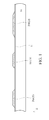
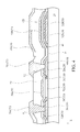
- FIG. 1 to FIG. 5 show schematic diagrams of a manufacturing method of an array substrate according to a first embodiment of the present invention
- FIG. 2 shows a schematic diagram of the manufacturing method following FIG. 1 ;
- FIG. 3 shows a schematic diagram of the manufacturing method following FIG. 2 ;
- FIG. 4 shows a schematic diagram of the manufacturing method following FIG. 3 ;
- FIG. 5 shows a schematic diagram of the manufacturing method following FIG. 4 ;
- FIG. 6 shows a schematic diagram of an array substrate according to a second embodiment of the present invention.
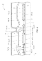
- FIG. 7 to FIG. 9 show schematic diagrams of a manufacturing method of an array substrate according to a third embodiment of the present invention.
- FIG. 8 shows a schematic diagram of the manufacturing method following FIG. 7 ;
- FIG. 9 shows a schematic diagram of the manufacturing method following FIG. 8 ;
- FIG. 10 shows a schematic diagram of an array substrate according to a fourth embodiment of the present invention.
- FIG. 11 and FIG. 12 show schematic diagrams of a manufacturing method of an array substrate according to a fifth embodiment of the present invention.
- FIG. 1 to FIG. 5 show schematic diagrams of a manufacturing method of an array substrate according to a first embodiment of the present invention.
- a substrate 10 is provided, and the substrate 10 may include a hard substrate, such as a glass substrate and a ceramic substrate, or a flexible substrate, such as a plastic substrate, or a substrate formed from another suitable material.
- a patterned auxiliary conductive layer 20 is formed over the substrate 10 , where the patterned auxiliary conductive layer 20 may include at least two etching stop patterns 20 A.
- the patterned auxiliary conductive layer 20 of this embodiment may further include a third electrode 20 B disposed apart from the etching stop patterns 20 A, where the two etching stop patterns 20 A are also disposed apart from each other.
- the patterned auxiliary conductive layer of this embodiment may be a single-layer or multi-layer structure, and materials thereof includes a metal, a metal oxide, an alloy, a transparent conductive material, a semiconductor material (for example, polycrystalline silicon, microcrystalline silicon, amorphous silicon, an oxide semiconductor, or another suitable material), or another suitable conductive material, or a combination of at least two of the foregoing materials.
- the foregoing metal material may include, for example, at least one of aluminum, copper, silver, chromium, titanium, and molybdenum, a composite layer of the foregoing material, a metal nitride of the foregoing material, a metal oxide of the foregoing material, or a metal oxynitride of the foregoing material, which, however, is not limited thereto.
- a buffer layer 11 may be selectively first formed over the substrate 10 , which, however, is not limited thereto.
- a material of the buffer layer 11 may include silicon oxide, silicon nitride, silicon oxynitride, or another suitable insulation material.
- a patterned semiconductor layer 30 is formed over the substrate 10 , and the patterned semiconductor layer 30 may include a semiconductor pattern 30 P that is disposed corresponding to an etching stop pattern 20 A.
- the semiconductor pattern 30 P covers the corresponding etching stop pattern 20 A and a part of a region between the two etching stop patterns 20 A.
- a region of a surface of the substrate 10 exposed by means of separation of the two etching stop patterns 20 A is covered by the semiconductor pattern 30 P, and the semiconductor pattern 30 P extends to cover the two etching stop patterns 20 A.
- the patterned semiconductor layer 30 may further include a first electrode 30 D formed over the third electrode 20 B of the patterned auxiliary conductive layer 20 , and the third electrode 20 B is in direct contact with and overlaps the first electrode 30 D in a vertical projection direction Z, which, however, is not limited thereto.
- the first electrode 30 D is separated from the patterned semiconductor layer 30 . It should be noted that the first electrode 30 D may be a pattern having relatively high conductivity after the patterned semiconductor layer 30 is subject to a local treatment.
- the patterned semiconductor layer 30 may include a polycrystalline silicon semiconductor material, an oxide semiconductor material, or another suitable semiconductor material, or a composition of the materials, and the first electrode 30 D may be a conductive pattern formed in a manner such as a local doping process or a local plasma treatment.
- the foregoing oxide semiconductor material may include a group II-VI compound (for example, zinc oxide, ZnO), a group II-VI compound doping with an alkaline earth metal (for example, magnesium-zinc oxide, ZnMgO), a group II-VI compound doping with an group IIIA element (for example, indium-gallium-zinc oxide, IGZO), a group II-VI compound doping with a group VA element (for example, tin-antimony oxide, SnSbO2), a group II-VI compound doping with a group VIA element (for example, zinc selenide oxide, ZnSeO), a group II-VI compound doping with a transition metal (for example, zinc-zirconium oxide, ZnZrO), or another oxide that is formed by mixing and combining the total element categories mentioned above and that has a semiconductor property, which, however, is not limited thereto.
- a group II-VI compound for example, zinc oxide, ZnO
- an alkaline earth metal for
- a gate dielectric layer 40 is formed between the patterned semiconductor layer 30 and the patterned auxiliary conductive layer 20 , and a first patterned conductive layer 50 is formed over the gate dielectric layer 40 .
- the gate dielectric layer 40 may be a single-layer or multiple-layer-stacked structure formed from silicon oxide, silicon nitride, silicon oxynitride, or another suitable insulation material.
- the first patterned conductive layer 50 includes a gate 50 A, disposed corresponding to the semiconductor pattern 30 P between the two etching stop patterns 20 A.
- the semiconductor pattern 30 P that is not affected by the local treatment becomes a channel region 30 A, and the channel region 30 A is located between the two heavily doped regions 30 B.
- Each etching stop pattern 20 A is in direct contact with and overlaps one heavily doped region 30 B in a vertical projection direction Z.
- the heavily doped regions 30 B may include a heavily doped region doped with a P-type dopant such as a boron ion or an N-type dopant such as a phosphorus ion, which, however, is not limited thereto.
- a lightly doped region 30 C between the heavily doped region 30 B and the channel region 30 A
- the gate 50 A corresponds to and overlaps the channel region 30 A in the vertical projection direction Z.
- a doping concentration of the heavily doped region is greater than that of the lightly doped region, and a channel region is generally an intrinsic region, which, however, is not limited thereto.
- the patterned auxiliary conductive layer 20 is formed before the patterned semiconductor layer 30 , so each etching stop pattern 20 A is located between the corresponding heavily doped region 30 B and the substrate 10 in a vertical projection direction Z.
- the first patterned conductive layer 50 of this embodiment may be a single-layer or multi-layer structure and includes a metal, an alloy, a transparent conductive material, or another suitable conductive material, or a combination of at least two of the foregoing materials, and this metal may include, for example, at least one of aluminum, copper, silver, chromium, titanium, and molybdenum, a composite layer of the foregoing material, a metal nitride of the foregoing material, a metal oxide of the foregoing material, or a metal oxynitride of the foregoing material, which, however, is not limited thereto.
- the first patterned conductive layer 50 may further include a second electrode 50 B, the first electrode 30 D and the second electrode 50 B overlap each other in the vertical projection direction Z, and a part of the gate dielectric layer 40 is disposed between the first electrode 30 D and the second electrode 50 B to form a storage capacitor CS.
- an interlayer dielectric layer 60 is formed over the gate dielectric layer 40 and the first patterned conductive layer 50 .
- the interlayer dielectric layer 60 may be a single-layer or multiple-layer-stacked structure formed from silicon oxide, silicon nitride, silicon oxynitride, or another suitable dielectric material.
- a plurality of first openings V 1 is formed by using, for example, a lithography etching process, and each first opening V 1 corresponds to one etching stop pattern 20 A.
- each first opening V 1 penetrates through the interlayer dielectric layer 60 , the gate dielectric layer 40 , and the patterned semiconductor layer 30 to at least partially expose the corresponding etching stop pattern 20 A.
- each first opening V 1 of this embodiment is preferably formed in a dry etching manner, which, however, is not limited thereto.
- a second patterned conductive layer 70 is formed over the interlayer dielectric layer 60 and in the first openings V 1 , the second patterned conductive layer 70 includes two source/drain electrodes 70 A, each source/drain electrode 70 A corresponds to one etching stop pattern 20 A, and each source/drain electrode 70 A passes through at least one first opening V 1 to come into contact with the corresponding etching stop pattern 20 A to form an electrical connection.
- the two source/drain electrodes 70 A are separated from each other.
- the second patterned conductive layer 70 of this embodiment may be a single-layer or multi-layer structure and includes a metal, an alloy, a transparent conductive material, or another suitable conductive material, or a combination of at least two of the foregoing materials, and this metal may include, for example, at least one of aluminum, copper, silver, chromium, titanium, and molybdenum, a composite layer of the foregoing material, a metal nitride of the foregoing material, a metal oxide of the foregoing material, or a metal oxynitride of the foregoing material, which, however, is not limited thereto.
- the second patterned conductive layer 70 may selectively further include a fourth electrode 70 B, the fourth electrode 70 B is disposed corresponding to the second electrode 50 B in the vertical projection direction Z, by means of which the fourth electrode 70 B, the second electrode 50 B, and the interlayer dielectric layer 60 sandwiched therebetwen to form another storage capacitor, which, however, is not limited thereto.
- a flat layer 80 is formed over the second patterned conductive layer 70 and the interlayer dielectric layer 60 .
- the flat layer 80 is of a single-layer or multi-layer material, which may include an inorganic material (for example, silicon nitride, silicon oxide, and silicon oxynitride, or another suitable material), an organic material (for example, acrylic resin, a photoresist, a color filter material, or another suitable material), or another suitable material.
- a second opening V 2 is formed, the second opening V 2 corresponds to one of the source/drain electrodes 70 A, and the second opening V 2 penetrates through the flat layer 80 to expose at least a part of the corresponding source/drain electrode 70 A.
- a pixel electrode 90 is formed over the flat layer 80 , and the pixel electrode 90 is in contact with the source/drain electrode 70 A exposed by the second opening V 2 to be connected thereto.
- an array substrate 101 as shown in FIG. 5 may be formed.
- a material of the pixel electrode 90 may differ depending on a property of a display device to which the pixel electrode 90 is applied.
- the pixel electrode 90 is preferably made from a transparent conductive material such as indium oxide
- the pixel electrode 90 may be made from a non-transparent conductive material such as a metal or an alloy
- the pixel electrode 90 may be partially made from a non-transparent conductive material such as a metal or an alloy, and another part thereof may be formed from a transparent conductive material, which, however, is not limited thereto.
- the transmissive display device, non-transmissive display device, and semi-transmissive display device all can be applied.
- the etching stop pattern 20 A having a conductive capability is disposed correspondingly below the heavily doped region 30 B of the patterned semiconductor layer 30 , when the first opening V 1 is formed, it is less required to concern a degree by which the patterned semiconductor layer 30 is damaged by an etching process, and the first opening V 1 may be enabled to directly penetrate through the patterned semiconductor layer 30 to directly expose a surface of the etching stop pattern 20 A, and the source/drain electrode 70 A may form an electrical connection to the heavily doped region 30 B by using the etching stop pattern 20 A having a conductive capability (for example, ohmic contact may be formed between the etching stop pattern 20 A and the heavily doped region 30 B), so the manufacturing method of this embodiment can achieve objectives such as enhancing the uniformity of electrical properties, increasing the process window, and improving the production yield.
- an array substrate 101 of this embodiment includes a substrate 10 , a patterned auxiliary conductive layer 20 , a patterned semiconductor layer 30 , a gate dielectric layer 40 , and a first patterned conductive layer 50 .
- the patterned auxiliary conductive layer 20 and the patterned semiconductor layer 30 are disposed over the substrate 10
- the patterned auxiliary conductive layer 20 includes two etching stop patterns 20 A
- the patterned semiconductor layer 30 includes a channel region 30 A and two heavily doped regions 30 B.
- the channel region 30 A is located between two heavily doped regions 30 B, and each etching stop pattern 20 A is in direct contact with and overlaps one heavily doped region 30 B in a vertical projection direction Z.
- the gate dielectric layer 40 is disposed over the patterned semiconductor layer 30 and the patterned auxiliary conductive layer 20 .
- the first patterned conductive layer 50 is disposed over the gate dielectric layer 40 , the first patterned conductive layer 50 includes a gate 50 A, and the gate 50 A is disposed corresponding to the channel region 30 A in the vertical projection direction Z.
- the patterned auxiliary conductive layer 20 is disposed between the substrate 10 and the patterned semiconductor layer 30 , and the etching stop pattern 20 A is disposed between the heavily doped region 30 B and the substrate 10 .
- the array substrate 101 may further include an interlayer dielectric layer 60 , a first opening V 1 , a second patterned conductive layer 70 , a flat layer 80 , a second opening V 2 , and a pixel electrode 90 .
- the interlayer dielectric layer 60 is disposed over the gate dielectric layer 40 and the first patterned conductive layer 50 , each first opening V 1 is disposed corresponding to one etching stop patterns 20 A, each first opening V 1 penetrates through the interlayer dielectric layer 60 , the gate dielectric layer 40 , and the patterned semiconductor layer 30 to at least partially expose the corresponding etching stop pattern 20 A.
- the second patterned conductive layer 70 is disposed over the interlayer dielectric layer 60 and in the first opening V 1 , the second patterned conductive layer 70 includes two source/drain electrodes 70 A, each source/drain electrode 70 A is disposed corresponding to one etching stop pattern 20 A, and each source/drain electrode 70 A passes through at least one first opening V 1 to come into contact with the corresponding etching stop pattern 20 A to form an electrical connection.
- the flat layer 80 is disposed over the second patterned conductive layer 70 and the interlayer dielectric layer 60 , the second opening V 2 is disposed corresponding to one source/drain electrode 70 A, and the second opening V 2 penetrates through the flat layer 80 to expose at least a part of the corresponding source/drain electrode 70 A.
- the pixel electrode 90 is disposed over the flat layer 80 , and the pixel electrode 90 is in contact with the source/drain electrode 70 A exposed by the second opening V 2 to form an electrical connection.
- a material property of each component in the array substrate 101 is described in the foregoing manufacturing method, and therefore, is not described again therein. It should be noted that because the patterned semiconductor layer 30 of this embodiment is formed after the patterned auxiliary conductive layer 20 , the third electrode 20 B of the patterned auxiliary conductive layer 20 is disposed between the first electrode 30 D and the substrate 10 .
- FIG. 6 shows a schematic diagram of an array substrate according to a second embodiment of the present invention.
- an array substrate 102 of this embodiment differs from the foregoing first embodiment, a patterned auxiliary conductive layer 20 of the array substrate 102 does not have the third electrode 20 B of the foregoing first embodiment, so a storage capacitor CS of this embodiment may only be formed from a first electrode 30 D and a second electrode 50 B of the patterned semiconductor layer 30 and a gate dielectric layer 40 sandwiched therebetween.
- FIG. 7 to FIG. 9 show schematic diagrams of a manufacturing method of an array substrate according to a third embodiment of the present invention.
- the patterned auxiliary conductive layer 20 of this embodiment is formed after the patterned semiconductor layer 30 , and each heavily doped region 30 B is located between a corresponding etching stop pattern 20 A and a substrate 10 in a vertical projection direction.
- the heavily doped region 30 and first electrode 30 D of this embodiment may be formed together by means of the same local treatment, for example, an ion implantation process, depending on requirements, which, however, is not limited thereto. Subsequently, as shown in FIG.
- a gate dielectric layer 40 and a first patterned conductive layer 50 are formed, and a lightly doped region 30 C is formed between the heavily doped region 30 B and a channel region 30 A by further utilizing another local treatment.
- an interlayer dielectric layer 60 , a first opening V 1 , a second patterned conductive layer 70 , a flat layer 80 , a second opening V 2 , and a pixel electrode 90 are subsequently formed, and further, an array substrate 103 as shown in FIG. 9 is formed.
- the patterned auxiliary conductive layer 20 is formed after the patterned semiconductor layer 30 , the patterned semiconductor layer 30 is disposed between the substrate 10 and the patterned auxiliary conductive layer 20 , and the etching stop pattern 20 A is disposed over the heavily doped region 30 B. Therefore, an etching process for forming the first opening V 1 in this embodiment stays on the etching stop pattern 20 A and the heavily doped region 30 B of the patterned semiconductor layer 30 would not be etched, so the heavily doped region 30 B can be protected by the etching stop pattern 20 A and would not be damaged.
- the first electrode 30 D is disposed between the third electrode 20 B of the patterned auxiliary conductive layer 20 and the substrate 10 , so the storage capacitor CS of this embodiment may be formed by the first electrode 30 D, the third electrode 20 B, the gate dielectric layer 40 , and the second electrode 50 B that are stacked over one another in sequence.
- FIG. 10 shows a schematic diagram of an array substrate according to a fourth embodiment of the present invention.
- an array substrate 104 of this embodiment differs from the foregoing third embodiment, a patterned auxiliary conductive layer 20 of the array substrate 104 does not have the third electrode 20 B of the foregoing third embodiment, so a storage capacitor CS of this embodiment may only be formed from a first electrode 30 D and a second electrode 50 B of the patterned semiconductor layer 30 and a gate dielectric layer 40 sandwiched therebetween.
- FIG. 11 and FIG. 12 show schematic diagrams of a manufacturing method of an array substrate according to a fifth embodiment of the present invention.
- a manufacturing method of an array substrate according to this embodiment includes the following steps. First, as shown in FIG. 11 , a patterned semiconductor layer 30 is formed over a substrate 10 , and the patterned semiconductor layer 30 includes a channel region 30 A and two heavily doped regions 30 B, and the channel region 30 A is located between the two heavily doped regions 30 B.
- the patterned semiconductor layer 30 may further include a first electrode 30 D formed over the substrate 10 , and the first electrode 30 D may be a pattern having relatively high conductivity after the patterned semiconductor layer 30 is subject to a local treatment.
- the patterned semiconductor layer 30 may include a polycrystalline silicon semiconductor material, an oxide semiconductor material, or another suitable semiconductor material, or a composition of the materials, and the first electrode 30 D may be a conductive pattern formed in a manner such as a local doping process or local plasma treatment.
- a buffer layer 11 may be selectively first formed over the substrate 10 , which, however, is not limited thereto.
- a material of the buffer layer 11 may include silicon oxide, silicon nitride, silicon oxynitride, or another suitable insulation material.
- a gate dielectric layer 40 is formed over the substrate 10 and the patterned semiconductor layer 30 , and a first patterned conductive layer 50 is formed over the gate dielectric layer 40 .
- the first patterned conductive layer 50 includes a gate 50 A, and the gate 50 A corresponds to and overlaps the channel region 30 A in a vertical projection direction Z.
- a lightly doped region 30 C may be formed between the heavily doped region 30 B and the channel region 30 A by further utilizing another local treatment.
- a doping concentration of the heavily doped region is greater than that of the lightly doped region, and a channel region is generally an intrinsic region, which, however, is not limited thereto.
- the first patterned conductive layer 50 may further include a second electrode 50 B, the first electrode 30 D and the second electrode 50 B overlap each other in the vertical projection direction Z, and a part of the gate dielectric layer 40 is disposed between the first electrode 30 D and the second electrode 50 B to form a storage capacitor CS.
- an interlayer dielectric layer 60 is formed between the gate dielectric layer 40 and the first patterned conductive layer 50 , a plurality of the first opening V 1 is formed, each first opening V 1 corresponds to one heavily doped region 30 B, and each first opening V 1 penetrates through the interlayer dielectric layer 60 , the gate dielectric layer 40 , and the corresponding heavily doped region 30 B to expose a surface of the substrate 10 .
- the gate dielectric layer 60 may further cover the second electrode 50 B.
- a patterned auxiliary conductive layer 21 is formed over the interlayer dielectric layer 60 and in the first openings V 1 , and a second patterned conductive layer 70 is formed over the patterned auxiliary conductive layer 21 .
- the second patterned conductive layer 70 is in direct contact with an upper surface of the patterned auxiliary conductive layer 21 .
- the patterned auxiliary conductive layer 21 includes two auxiliary conductive patterns 21 A, each auxiliary conductive pattern 21 A is conformally formed in one first opening, and each auxiliary conductive pattern 21 A is in contact with the heavily doped region 30 B exposed by the corresponding first opening V 1 to form an electrical connection.
- the second patterned conductive layer 70 includes two source/drain electrodes 70 A, one first opening V 1 is filled with each source/drain electrode 70 A, and each source/drain electrode 70 A forms an electrical connection to one heavily doped region 30 B by using the auxiliary conductive pattern 21 A in the corresponding first opening V 1 .
- the patterned auxiliary conductive layer 21 may preferably include a heavily doped polycrystalline silicon layer, microcrystalline silicon layer, or amorphous silicon layer, or another suitable conductive material, or metal oxide material or a combination of at least two of the foregoing materials, and the patterned auxiliary conductive layer 21 and the second patterned conductive layer 70 may be formed together by using the same patterning process, for example, a yellow light etching process, by means of which an effect of simplifying a process is produced, which, however, is limited thereto.
- the patterned auxiliary conductive layer 21 and the second patterned conductive layer 70 may also be separately formed by means of different patterning processes depending on requirements.
- the patterned auxiliary conductive layer 21 may further include a fifth electrode 21 B disposed between a fourth electrode 70 B of the second patterned conductive layer 70 and the interlayer dielectric layer 60 , that is, the fourth electrode 70 B is in direct contact with an upper surface of the fifth electrode 21 B. Therefore, the interlayer dielectric layer 60 is disposed between the fifth electrode 21 B and the second electrode 50 B to form another storage capacitor CS.
- a flat layer 80 , a second opening V 2 , and a pixel electrode 90 may be further formed, and further, an array substrate 105 as shown in FIG. 12 is formed.
- the flat layer 80 is formed over the second patterned conductive layer 70 and the interlayer dielectric layer 60 , the second opening V 2 corresponds to one source/drain electrode 70 A, and the second opening V 2 penetrates through the flat layer 80 to expose at least a part of the corresponding source/drain electrode 70 A.
- the pixel electrode 90 is formed over the flat layer 80 , and the pixel electrode 90 is in contact with the source/drain electrode 70 A exposed by the second opening V 2 to form an electrical connection. It should be noted that the flat layer 80 may further cover the fourth electrode 70 B.
- the array substrate 105 of this embodiment includes a substrate 10 , a buffer layer 11 , a patterned semiconductor layer 30 , a gate dielectric layer 40 , a first patterned conductive layer 50 , an interlayer dielectric layer 60 , a plurality of first openings V 1 , a patterned auxiliary conductive layer 21 , and a second patterned conductive layer 70 .
- the patterned semiconductor layer 30 is disposed over the substrate 10 , the patterned semiconductor layer 30 includes a channel region 30 A and two heavily doped regions 30 B, and the channel region 30 A is located between the two heavily doped regions 30 B.
- the gate dielectric layer 40 is disposed over the substrate 10 and the patterned semiconductor layer 30 .
- the first patterned conductive layer 50 is disposed over the gate dielectric layer 40 , the first patterned conductive layer 50 includes a gate 50 A, and the gate 50 A is disposed corresponding to the channel region 30 A in a vertical projection direction Z.
- the interlayer dielectric layer 60 is disposed over the gate dielectric layer 40 and the first patterned conductive layer 50 .
- Each first opening V 1 is disposed corresponding to one heavily doped region 30 B, and each first opening V 1 penetrates through the interlayer dielectric layer 60 , the gate dielectric layer 40 , and the corresponding heavily doped region 30 B.
- the patterned auxiliary conductive layer 21 is disposed over the interlayer dielectric layer 60 and in the first openings V 1 , the patterned auxiliary conductive layer 21 includes two auxiliary conductive patterns 21 A, each auxiliary conductive pattern 21 A is conformally disposed in one first opening V 1 , and each auxiliary conductive pattern 21 A is in contact with the heavily doped region 30 B exposed by the corresponding first opening V 1 to form an electrical connection.
- the second patterned conductive layer 70 is disposed over the patterned auxiliary conductive layer 21 , the second patterned conductive layer 70 includes two source/drain electrodes 70 A, one first opening V 1 is filled with each source/drain electrode 70 A, and each source/drain electrode 70 A forms an electrical connection to one heavily doped region 30 B by using the auxiliary conductive pattern 21 A in the corresponding first opening V 1 .
- the array substrate 105 may further include a flat layer 80 A, a second opening V 2 , and a pixel electrode 90 .
- the flat layer 80 is disposed over the second patterned conductive layer 70 and the interlayer dielectric layer 60 , the second opening V 2 is disposed corresponding to one source/drain electrode 70 A, and the second opening V 2 penetrates through the flat layer 80 to expose at least a part of the corresponding source/drain electrode 70 A.
- the pixel electrode 90 is disposed over the flat layer 80 , and the pixel electrode 90 is in contact with the source/drain electrode 70 A exposed by the second opening V 2 to form an electrical connection.
- the array substrate 105 may further include a storage capacitor CS, and the storage capacitor CS may formed by a first electrode 30 D of the patterned semiconductor layer 30 , a second electrode 50 B of the first patterned conductive layer 50 , and the gate dielectric layer 40 sandwiched between the first electrode 30 D and the second electrode 50 B, which, however, is not limited thereto.
- the interlayer dielectric layer 60 is disposed between a fifth electrode 21 B and the second electrode 50 B to form another storage capacitor CS.
- the source/drain electrode 70 A forms an electrical connection to the heavily doped region 30 by using the auxiliary conductive pattern 21 A
- the auxiliary conductive pattern 21 A may preferably be of a conductive material the same as that if the heavily doped region 30 B, for example, a heavily doped polycrystalline silicon layer, even if the heavily doped region 30 B is etched when during an etching process for forming the first openings V 1 , there is still a favorable conducting state between the auxiliary conductive pattern 21 A and the heavily doped region 30 B.
- auxiliary conductive layer 21 and the second patterned conductive layer 70 are formed together by means of the same yellow light etching process, contact surfaces of the source/drain electrode 70 A and the auxiliary conductive pattern 21 A are not damaged by the etching and may maintain a favorable contact state (for example, the ohmic contact).
- an electric connection state between the source/drain electrode 70 A and the heavily doped region 30 B may be ensured by disposing the auxiliary conductive pattern 21 A, so that it is less required to concern a degree by which the patterned semiconductor layer 30 is damaged when the first openings V 1 are formed.
- the manufacturing method of this embodiment can achieve objectives such as enhancing the uniformity of electrical properties, increasing the process window, and improving the production yield.
- an etching stop pattern or auxiliary conductive pattern of a patterned auxiliary conductive layer is electrically connected to a source/drain electrode and a heavily doped region, so as to alleviate influence of an unfavorable electrical property caused by that the heavily doped region is damaged by etching, thereby achieving objectives such as enhancing the uniformity of electrical properties, increasing the process window, and improving the production yield.
Landscapes
- Thin Film Transistor (AREA)
- Engineering & Computer Science (AREA)
- Manufacturing & Machinery (AREA)
- Chemical & Material Sciences (AREA)
- Crystallography & Structural Chemistry (AREA)
Applications Claiming Priority (3)
| Application Number | Priority Date | Filing Date | Title |
|---|---|---|---|
| TW105101598A TWI572020B (zh) | 2016-01-19 | 2016-01-19 | 陣列基板以及其製作方法 |
| TW105101598A | 2016-01-19 | ||
| TW105101598 | 2016-01-19 |
Publications (2)
| Publication Number | Publication Date |
|---|---|
| US20170207253A1 US20170207253A1 (en) | 2017-07-20 |
| US10615188B2 true US10615188B2 (en) | 2020-04-07 |
Family
ID=56388453
Family Applications (1)
| Application Number | Title | Priority Date | Filing Date |
|---|---|---|---|
| US15/374,379 Active 2037-05-22 US10615188B2 (en) | 2016-01-19 | 2016-12-09 | Array substrate and manufacturing method thereof |
Country Status (3)
| Country | Link |
|---|---|
| US (1) | US10615188B2 (zh) |
| CN (1) | CN105789217B (zh) |
| TW (1) | TWI572020B (zh) |
Cited By (1)
| Publication number | Priority date | Publication date | Assignee | Title |
|---|---|---|---|---|
| US11355569B2 (en) | 2019-12-10 | 2022-06-07 | Au Optronics Corporation | Active device substrate comprising silicon layer and manufacturing method thereof |
Families Citing this family (7)
| Publication number | Priority date | Publication date | Assignee | Title |
|---|---|---|---|---|
| KR102641816B1 (ko) * | 2016-07-19 | 2024-02-29 | 삼성디스플레이 주식회사 | 디스플레이 장치 |
| KR102405404B1 (ko) * | 2017-06-13 | 2022-06-07 | 삼성디스플레이 주식회사 | 표시 장치 및 표시 장치의 제조 방법 |
| CN108806593A (zh) * | 2018-05-31 | 2018-11-13 | 厦门天马微电子有限公司 | 一种有机发光显示面板及显示装置 |
| CN118763123A (zh) * | 2019-09-24 | 2024-10-11 | 乐金显示有限公司 | 薄膜晶体管及其基板及包括该薄膜晶体管的显示设备 |
| TWI743899B (zh) * | 2020-07-22 | 2021-10-21 | 友達光電股份有限公司 | 元件陣列基板及其製作方法 |
| CN113889488B (zh) * | 2021-09-18 | 2025-08-26 | 厦门天马显示科技有限公司 | 显示面板及显示装置 |
| CN115224050B (zh) * | 2022-06-30 | 2026-03-06 | 昆山国显光电有限公司 | 一种阵列基板及制备方法和显示面板 |
Citations (7)
| Publication number | Priority date | Publication date | Assignee | Title |
|---|---|---|---|---|
| US20040129943A1 (en) * | 2002-12-31 | 2004-07-08 | Yoo Soon Sung | Thin film transistor array substrate and manufacturing method of the same |
| US20070103610A1 (en) | 2005-11-09 | 2007-05-10 | Lg.Philips Lcd Co., Ltd. | Array substrate for liquid crystal display device and method of fabricating the same |
| US7863120B2 (en) | 2001-03-21 | 2011-01-04 | Lg Display Co., Ltd. | Liquid crystal display device with double metal layer source and drain electrodes and fabricating method thereof |
| US7939828B2 (en) * | 2007-04-12 | 2011-05-10 | Au Optronics Corporation | Pixel structure and method for fabricating the same |
| CN104009043A (zh) | 2014-03-27 | 2014-08-27 | 友达光电股份有限公司 | 像素结构及其制作方法 |
| US20160079429A1 (en) * | 2014-09-16 | 2016-03-17 | Carolyn Rae Ellinger | Top gate tft with polymer interface control layer |
| US20170062484A1 (en) * | 2015-08-28 | 2017-03-02 | United Microelectronics Corp. | Semiconductor device and method for forming the same |
Family Cites Families (5)
| Publication number | Priority date | Publication date | Assignee | Title |
|---|---|---|---|---|
| KR100720095B1 (ko) * | 2000-11-07 | 2007-05-18 | 삼성전자주식회사 | 박막 트랜지스터 어레이 기판 및 그 제조 방법 |
| US20080191207A1 (en) * | 2007-02-08 | 2008-08-14 | Mitsubishi Electric Corporation | Thin film transistor device, method of manufacturing the same, and display apparatus |
| KR101213708B1 (ko) * | 2009-06-03 | 2012-12-18 | 엘지디스플레이 주식회사 | 어레이 기판 및 이의 제조방법 |
| CN103454798B (zh) * | 2013-08-30 | 2017-01-25 | 合肥京东方光电科技有限公司 | 阵列基板及其制作方法、显示装置 |
| KR102227474B1 (ko) * | 2013-11-05 | 2021-03-15 | 삼성디스플레이 주식회사 | 박막트랜지스터 어레이 기판, 유기발광표시장치 및 박막트랜지스터 어레이 기판의 제조 방법 |
-
2016
- 2016-01-19 TW TW105101598A patent/TWI572020B/zh active
- 2016-03-10 CN CN201610135524.0A patent/CN105789217B/zh active Active
- 2016-12-09 US US15/374,379 patent/US10615188B2/en active Active
Patent Citations (8)
| Publication number | Priority date | Publication date | Assignee | Title |
|---|---|---|---|---|
| US7863120B2 (en) | 2001-03-21 | 2011-01-04 | Lg Display Co., Ltd. | Liquid crystal display device with double metal layer source and drain electrodes and fabricating method thereof |
| US20040129943A1 (en) * | 2002-12-31 | 2004-07-08 | Yoo Soon Sung | Thin film transistor array substrate and manufacturing method of the same |
| US20070103610A1 (en) | 2005-11-09 | 2007-05-10 | Lg.Philips Lcd Co., Ltd. | Array substrate for liquid crystal display device and method of fabricating the same |
| CN1964056A (zh) | 2005-11-09 | 2007-05-16 | Lg.菲利浦Lcd株式会社 | 液晶显示器件的阵列基板及其制造方法 |
| US7939828B2 (en) * | 2007-04-12 | 2011-05-10 | Au Optronics Corporation | Pixel structure and method for fabricating the same |
| CN104009043A (zh) | 2014-03-27 | 2014-08-27 | 友达光电股份有限公司 | 像素结构及其制作方法 |
| US20160079429A1 (en) * | 2014-09-16 | 2016-03-17 | Carolyn Rae Ellinger | Top gate tft with polymer interface control layer |
| US20170062484A1 (en) * | 2015-08-28 | 2017-03-02 | United Microelectronics Corp. | Semiconductor device and method for forming the same |
Non-Patent Citations (1)
| Title |
|---|
| State Intellectual Property Office of the People's Republic of China, "Office Action", dated Apr. 19, 2018. |
Cited By (1)
| Publication number | Priority date | Publication date | Assignee | Title |
|---|---|---|---|---|
| US11355569B2 (en) | 2019-12-10 | 2022-06-07 | Au Optronics Corporation | Active device substrate comprising silicon layer and manufacturing method thereof |
Also Published As
| Publication number | Publication date |
|---|---|
| US20170207253A1 (en) | 2017-07-20 |
| CN105789217B (zh) | 2019-04-19 |
| CN105789217A (zh) | 2016-07-20 |
| TWI572020B (zh) | 2017-02-21 |
| TW201727879A (zh) | 2017-08-01 |
Similar Documents
| Publication | Publication Date | Title |
|---|---|---|
| US10615188B2 (en) | Array substrate and manufacturing method thereof | |
| US20200105789A1 (en) | Array substrate, method of manufacturing the same, and display panel | |
| TWI438868B (zh) | 互補金氧半電晶體及其製作方法 | |
| US20110266542A1 (en) | Semiconductor device and method of fabricating the same | |
| US11121226B2 (en) | Thin film transistor and method for manufacturing the same, array substrate and display device | |
| CN106558594A (zh) | 阵列基板、显示面板、显示装置及制备方法 | |
| CN103456740A (zh) | 像素单元及其制造方法、阵列基板和显示装置 | |
| US11183610B2 (en) | Photoelectric detector, preparation method thereof, display panel and display device | |
| US9437742B2 (en) | Thin film transistor, manufacturing method thereof and array substrate | |
| CN107946324B (zh) | 光感测装置 | |
| KR101955336B1 (ko) | 광 센싱 트랜지스터, 이의 제조방법 및 이를 채용한 디스플레이 패널 | |
| US9276126B2 (en) | Semiconductor device and method for producing same | |
| US20140027760A1 (en) | Semiconductor device and manufacturing method thereof | |
| US20130077012A1 (en) | Semiconductor device and method for manufacturing the same, and liquid crystal display device | |
| US6646308B2 (en) | Flat panel display device | |
| KR20180085850A (ko) | 트랜지스터 표시판 및 그 제조 방법 | |
| US20150187830A1 (en) | Photosensitive unit, array substrate of display panel and manufacturing method thereof | |
| KR20150089299A (ko) | 디스플레이 소자, 그 제조 방법, 및 이미지 센서 소자의 제조방법 | |
| CN203502708U (zh) | 像素单元、阵列基板和显示装置 | |
| US9461066B2 (en) | Thin film transistor and method of manufacturing the same, array substrate and display device | |
| US9793302B1 (en) | Active device | |
| US11569406B2 (en) | Pin device and manufacturing method thereof, photosensitive device and display device | |
| US9379250B2 (en) | Semiconductor device and method for producing same | |
| US11307468B2 (en) | Array substrate and manufacturing method thereof | |
| US9276127B2 (en) | Semiconductor device and method for producing same |
Legal Events
| Date | Code | Title | Description |
|---|---|---|---|
| AS | Assignment |
Owner name: AU OPTRONICS CORPORATION, TAIWAN Free format text: ASSIGNMENT OF ASSIGNORS INTEREST;ASSIGNORS:LIU, CHAN-JUI;LIN, YU-LING;SHAN, CHIEN-HSUN;AND OTHERS;SIGNING DATES FROM 20161020 TO 20161021;REEL/FRAME:040700/0931 |
|
| STPP | Information on status: patent application and granting procedure in general |
Free format text: PUBLICATIONS -- ISSUE FEE PAYMENT VERIFIED |
|
| STPP | Information on status: patent application and granting procedure in general |
Free format text: DOCKETED NEW CASE - READY FOR EXAMINATION |
|
| STPP | Information on status: patent application and granting procedure in general |
Free format text: NON FINAL ACTION MAILED |
|
| STPP | Information on status: patent application and granting procedure in general |
Free format text: RESPONSE TO NON-FINAL OFFICE ACTION ENTERED AND FORWARDED TO EXAMINER |
|
| STPP | Information on status: patent application and granting procedure in general |
Free format text: FINAL REJECTION MAILED |
|
| STPP | Information on status: patent application and granting procedure in general |
Free format text: ADVISORY ACTION MAILED |
|
| STPP | Information on status: patent application and granting procedure in general |
Free format text: NOTICE OF ALLOWANCE MAILED -- APPLICATION RECEIVED IN OFFICE OF PUBLICATIONS |
|
| STPP | Information on status: patent application and granting procedure in general |
Free format text: PUBLICATIONS -- ISSUE FEE PAYMENT VERIFIED |
|
| STCF | Information on status: patent grant |
Free format text: PATENTED CASE |
|
| MAFP | Maintenance fee payment |
Free format text: PAYMENT OF MAINTENANCE FEE, 4TH YEAR, LARGE ENTITY (ORIGINAL EVENT CODE: M1551); ENTITY STATUS OF PATENT OWNER: LARGE ENTITY Year of fee payment: 4 |