TWI867716B - Electronic component, intermediary mechanism, testing device, and processing machine - Google Patents
Electronic component, intermediary mechanism, testing device, and processing machine Download PDFInfo
- Publication number
- TWI867716B TWI867716B TW112132596A TW112132596A TWI867716B TW I867716 B TWI867716 B TW I867716B TW 112132596 A TW112132596 A TW 112132596A TW 112132596 A TW112132596 A TW 112132596A TW I867716 B TWI867716 B TW I867716B
- Authority
- TW
- Taiwan
- Prior art keywords
- electronic component
- substrate
- intermediary
- pressure
- intermediate layer
- Prior art date
Links
Images


Landscapes
- Testing Of Individual Semiconductor Devices (AREA)
Abstract
Description
本發明提供一種具有中介層之電子元件,以使電子元件均勻受壓測試,進而提高測試品質之電子元件、中介機構、測試裝置及作業機。The present invention provides an electronic component with an intermediate layer, so that the electronic component can be evenly stressed during testing, thereby improving the test quality of the electronic component, intermediate mechanism, test device and operating machine.
在現今,電子元件於製作完成後,必須以測試裝置進行測試作業而淘汰不良品。測試裝置以測試器承置及測試電子元件,並利用壓接器之下壓治具以預設下壓力壓接電子元件之頂面而執行測試作業。然,部份電子元件之頂面呈凹弧狀或凸弧狀等非平面型態,當壓接器以一底面呈平面狀之下壓治具壓接一頂面呈凹弧狀或凸弧狀的電子元件時,下壓治具之底面完全無法貼合電子元件之頂面,導致壓接器無法平均施力壓接電子元件,以致電子元件受力不均,致使電子元件之部分接點無法確實接觸測試器之探針,進而影響測試準確性及品質。Nowadays, after the electronic components are manufactured, they must be tested by testing equipment to eliminate defective products. The testing equipment uses a tester to hold and test the electronic components, and uses the lower pressing fixture of the crimper to press the top surface of the electronic components with a preset lower pressure to perform the testing operation. However, the top surfaces of some electronic components are non-planar shapes such as concave arcs or convex arcs. When the crimper uses a lower pressing fixture with a flat bottom surface to press an electronic component with a concave arc or convex arc top surface, the bottom surface of the lower pressing fixture cannot fit the top surface of the electronic component at all, resulting in the crimper being unable to apply force evenly to press the electronic component, causing the electronic component to be unevenly stressed, causing some contacts of the electronic component to be unable to accurately contact the probe of the tester, thereby affecting the test accuracy and quality.
本發明之目的一,提供一種電子元件,包含基體及至少一中介層 ;基體設有至少一接點,而頂面呈曲弧狀;至少一中介層作可卸除式設置於基體之頂面,並具有相對之承壓面及貼合面,承壓面呈平面狀,以供承受下壓力 ,貼合面貼覆於基體之頂面;藉以電子元件利用中介層之承壓面均勻承受下壓力而執行測試作業,於完成測試後卸除中介層,進而提高電子元件之測試品質。 The first object of the present invention is to provide an electronic component, comprising a substrate and at least one intermediate layer. The substrate is provided with at least one contact, and the top surface is curved. At least one intermediate layer is detachably arranged on the top surface of the substrate, and has a pressure-bearing surface and a bonding surface opposite to each other. The pressure-bearing surface is flat to bear the downward pressure, and the bonding surface is attached to the top surface of the substrate. The electronic component uses the pressure-bearing surface of the intermediate layer to evenly bear the downward pressure to perform the test operation, and the intermediate layer is removed after the test is completed, thereby improving the test quality of the electronic component.
本發明之目的二,提供一種中介機構,包含至少一承置器、至少一塗覆器及至少一固化器;承置器以供承置電子元件之基體;塗覆器以供於電子元件呈曲弧狀之頂面塗覆具平面狀承壓面之中介層;固化器以供固化電子元件之中介層而可承受下壓力;藉以中介機構能夠於電子元件設置固化狀態之中介層,以利電子元件均勻承受下壓力而執行測試作業,於完成測試後卸除中介層,進而提高電子元件測試品質。The second object of the present invention is to provide an intermediate mechanism, including at least one support, at least one coater and at least one curing device; the support is used to support the substrate of the electronic component; the coater is used to coat the curved top surface of the electronic component with an intermediate layer having a flat pressure-bearing surface; the curing device is used to cure the intermediate layer of the electronic component so that it can withstand downward pressure; the intermediate mechanism can set the intermediate layer in a cured state on the electronic component, so that the electronic component can evenly withstand the downward pressure to perform the test operation, and the intermediate layer is removed after the test is completed, thereby improving the test quality of the electronic component.
本發明之目的三,提供一種中介機構,更包含至少一軟化器,軟化器可於電子元件完成測試作業後,而供軟化中介層,以利卸除電子元件上之中介層,進而提高使用便利性。The third object of the present invention is to provide an intermediary mechanism, further comprising at least one softener, which can soften the intermediary layer after the electronic component completes the testing operation, so as to facilitate the removal of the intermediary layer on the electronic component, thereby improving the convenience of use.
本發明之目的四,提供一種中介機構,更包含至少一清除器,清除器可於中介層軟化後,將中介層與電子元件分離卸除,以利電子元件執行後續作業。The fourth object of the present invention is to provide an interposer mechanism, further comprising at least one cleaner, which can separate and remove the interposer from the electronic component after the interposer is softened, so as to facilitate subsequent operations on the electronic component.
本發明之目的五,提供一種測試裝置,包含測試機構、壓接機構及中介機構;測試機構設置至少一測試器,以供測試電子元件;壓接機構設置至少一壓接器,以供壓接測試器之電子元件;中介機構設置承置器、塗覆器及固化器,以供於電子元件呈曲弧狀之頂面塗覆及固化具有平面狀承壓面之中介層,以供壓接器平均施力壓接電子元件,進而提高測試良率。The fifth object of the present invention is to provide a testing device, including a testing mechanism, a crimping mechanism and an intermediate mechanism; the testing mechanism is provided with at least one tester for testing electronic components; the crimping mechanism is provided with at least one crimper for crimping the electronic components of the tester; the intermediate mechanism is provided with a holder, a coater and a curing device for coating and curing an intermediate layer with a flat pressure-bearing surface on the curved top surface of the electronic component, so that the crimper can apply an even force to crimp the electronic component, thereby improving the test yield.
本發明之目的六,提供一種作業機,包含機台、供料裝置、收料裝置、測試裝置、輸送裝置及中央控制裝置,供料裝置配置於機台,並設有至少一供料器,以供容置至少一待測電子元件;收料裝置配置於機台,並設有至少一收料器,以供容置至少一已測電子元件;測試裝置配置於機台,並設有測試機構、壓接機構及中介機構,以供測試電子元件;輸送裝置配置於機台,並設有至少一輸送器,以供輸送電子元件;中央控制裝置以控制及整合各裝置作動而執行自動化作業。The sixth object of the present invention is to provide an operating machine, comprising a machine, a feeding device, a receiving device, a testing device, a conveying device and a central control device, wherein the feeding device is arranged on the machine and is provided with at least one feeder for accommodating at least one electronic component to be tested; the receiving device is arranged on the machine and is provided with at least one receiver for accommodating at least one tested electronic component; the testing device is arranged on the machine and is provided with a testing mechanism, a crimping mechanism and an intermediate mechanism for testing electronic components; the conveying device is arranged on the machine and is provided with at least one conveyor for conveying electronic components; the central control device controls and integrates the actions of each device to perform automated operations.
為使 貴審查委員對本發明作更進一步之瞭解,茲舉一較佳實施例並配合圖式,詳述如後:In order to enable you to have a further understanding of the present invention, a preferred embodiment is given below with accompanying drawings:
請參閱圖1,本發明電子元件10包含基體11及至少一中介層12。Referring to FIG. 1 , the
基體11設有至少一接點,而頂面呈曲弧狀;依電子元件之型式,基體11之接點可為錫球或接腳,於頂面呈凹弧狀或凸弧狀。於本實施例,電子元件10之基體11於底面111設有複數個為錫球之接點112,以供電性連接測試座(圖未示出),而基體11之頂面113呈凹弧狀。The
至少一中介層12設置於基體11之頂面113,並具有相對之貼合面121及承壓面122,貼合面121貼覆於基體11之頂面113,承壓面122呈平面狀,以供承受下壓力。更進一步,中介層12作可卸除式配置於基體11之頂面113。At least one
於本實施例,中介層12可為熱塑性塑膠、光固化樹脂或低溫合金等材質,中介層12之底面為貼合面121,而頂面則為承壓面122,中介層12之貼合面121貼接於基體11之頂面113,於中介層12尚未固化時,其貼合面121可隨著基體11之頂面113的凹弧狀而作一貼合變形,以完全貼合覆蓋於基體11之頂面113,中介層12之承壓面122為一平面狀,於中介層12固化時,承壓面122可承受一下壓力。In this embodiment, the
更進一步,於解除中介層12之下壓力後,中介層12能夠受高溫軟化而易於脫離基體11,加以於基體11上卸除中介層12。Furthermore, after the pressure under the
請參閱圖2至圖6,本發明之中介機構應用於在電子元件10設置中介層12,中介機構包含至少一承置器、至少一塗覆器及至少一固化器;至少一承置器以供承置電子元件10之基體11;至少一塗覆器以供於電子元件10之基體11呈曲弧狀的頂面113塗覆中介層12,中介層12具有呈平面狀之承壓面122;至少一固化器以供固化電子元件10之中介層12,中介層12之承壓面122能夠承受下壓力。Please refer to Figures 2 to 6. The intermediary mechanism of the present invention is applied to set an
依作業需求,中介機構可於電子元件10移入測試器之前,先行於基體11上設置中介層12,或者於電子元件10之基體11置入測試器且尚未測試前
,而於基體11上設置中介層12,不受限於本實施例。
According to the operation requirements, the intermediary mechanism can set the
依作業需求,電子元件10可於完成測試作業後,由輸送器搬移至其他裝置或作業機執行卸除中介層12之作業,或者中介機構配置有軟化器或/及清除器,並依作動時序於同一作業機上執行軟化或/及清除中介層12之作業,不受限於本實施例。According to the operation requirements, the
依作業需求,承置器可為獨立之承座或測試座,以供承置電子元件10。於本實施例,承置器為獨立之承座21,承座21以供輸送器(圖未示出)移入電子元件10之基體11。According to the operation requirements, the holder can be an independent holder or a test holder for holding the
塗覆器22由塗覆驅動器(圖未示出)驅動作至少一方向位移,以對電子元件10塗覆中介層12;依作業需求,塗覆器22可供輸入具有用以形成中介層12之材料,材料可為熱塑性塑膠、光固化樹脂或低溫合金等,材料之特性具有於測試前可被固化於電子元件10之基體11的頂面113而形成中介層12,以及於測試後可被軟化而由基體11上加以卸除。於本實施例,塗覆器22以供輸入可為光固化樹脂之材料,並由塗覆驅動器驅動位移至承座21之上方,而對電子元件10之基體11執行塗覆作業,以將光固化樹脂塗覆於基體11的頂面113而形成中介層12,中介層12之一面為呈平面狀且朝向上方之承壓面122,而另一相對面為朝向下方且完全貼合基體11之頂面113的貼合面121。The
依作業需求,固化器23可為光固化器或冷卻器等,以光照射方式或冷卻方式而固化電子元件10之中介層12;例如固化器23為光固化器,以紫外線光照射可為光固化樹脂之中介層12固化;例如固化器23為冷卻器,以低溫冷卻可為熱塑性塑膠之中介層12固化。更進一步,固化器23可配置於承置器之周側或上方,或由固化驅動器(圖未示出)驅動位移至承置器之周側或上方,用以對承置器上之電子元件10的中介層12執行固化作業。於本實施例,固化器23具有至少一紫外線光燈具,並由固化驅動器驅動位移至承座21之上方,以紫外線光燈具照射電子元件10之中介層12固化,使電子元件10能夠利用中介層12之呈平面狀的承壓面122承受一下壓力。According to the operation requirements, the
依作業需求,中介機構更包含軟化器,軟化器以供軟化電子元件10上之中介層12。更進一步,軟化器具有至少一加熱件,以軟化中介層12。According to the operation requirements, the interposer mechanism further includes a softener for softening the
依作業需求,中介機構更包含清除器,清除器以供卸除電子元件10上之中介層12。更進一步,清除器可為吸取器、夾具或刷具等。According to the operation requirements, the intermediary mechanism further includes a remover, which is used to remove the
本發明之中介機構應用於測試裝置20,測試裝置20包含測試機構
、壓接機構及中介機構,測試機構設置至少一測試器,以供測試電子元件10;壓接機構設置至少一壓接器,以供壓接測試器之電子元件10;中介機構以供於電子元件10之基體11的頂面113塗覆具平面狀承壓面122之中介層12,並固化中介層12,使電子元件10以中介層12的承壓面122能夠均勻承受壓接器之下壓力。
The intermediary mechanism of the present invention is applied to a
依作業需求,壓接機構更包含至少一溫控器,以供溫控電子元件 。溫控器可配置於壓接器之上方、壓接器或下壓治具,並設有至少一溫控件,以供電子元件於模擬日後應用溫度環境執行測試作業。更進一步,溫控件可為加熱件、致冷晶片或具流體之座體。 According to the operation requirements, the crimping mechanism further includes at least one temperature controller for temperature control of electronic components. The temperature controller can be arranged above the crimper, the crimper or the lower pressing fixture, and is provided with at least one temperature control part for the electronic components to perform test operations in the simulated future application temperature environment. Furthermore, the temperature control part can be a heating element, a cooling chip or a seat with a fluid.
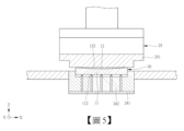
於本實施例,測試機構之測試器包含電性連接之電路板241及測試座242,測試座242具有複數支探針,並供承置及測試電子元件10。壓接機構配置於測試機構之上方,並設有可由壓接驅動器(圖未示出)驅動作至少一方向(例如Z方向)位移之壓接器25,壓接器25具有底面呈平面狀之下壓治具251,以供壓接電子元件10。更進一步,壓接驅動器為壓缸、線性馬達或包含馬達及至少一傳動組,傳動組為皮帶輪組或螺桿螺座組等。In this embodiment, the tester of the testing mechanism includes an electrically connected
於本實施例,一輸送器(圖未示出)將具有基體11及中介層12之電子元件10移入測試機構之測試座242,令基體11的接點112朝向下方且接觸測試座242之探針,並使中介層12的承壓面122朝向上方;壓接機構以壓接驅動器(圖未示出)驅動壓接器25作Z方向向下位移,壓接器25之下壓治具251以預設下壓力壓接電子元件10之中介層12的承壓面122,由於中介層12的承壓面122為一平面狀,而可使壓接器25之下壓治具251完全貼合中介層12之承壓面122,而平均施力壓接電子元件10,在電子元件10均勻承受下壓力之狀態下,使得電子元件10之基體11的接點112確實電性接觸測試座242之探針而作有效性執行測試作業,進而提高測試良率。In this embodiment, a conveyor (not shown) moves the
於測試完畢,一輸送器(圖未示出)於測試座242取出具中介層12之電子元件10,並移載至中介機構之承座21。After the test is completed, a conveyor (not shown) takes out the
中介機構設置有軟化器26,以供軟化電子元件10之中介層12;例如軟化器26為一高溫箱體,以供置入電子元件10,而加以軟化中介層12;例如軟化器26具有加熱件,以加熱件接觸軟化中介層12,不受限於本實施例。於本實施例,軟化器26於靠近底部處設置加熱件261,中介機構以軟化驅動器(圖未示出)驅動軟化器26位移至電子元件10之上方,軟化器26之底面接觸電子元件10之中介層12,以傳導加熱件261之高溫而軟化電子元件10之中介層12,使中介層12處於軟化且可利於脫離電子元件10之基體11的狀態。The intermediate mechanism is provided with a
當電子元件10之中介層12呈軟化狀態時,中介機構設置有清除器27,以卸除電子元件10上之中介層12;中介機構以清除驅動器(圖未示出)驅動清除器27位移至電子元件10之上方,令清除器27清除基體11上之中介層12,以利電子元件10進行下一製程或出料收置。When the
依作業需求,中介機構之軟化器26亦可整合配置於壓接機構之壓接器25,於測試完畢後,利用位於壓接器25上之軟化器26對電子元件10之中介層12執行軟化作業,亦無不可。According to the operation requirements, the
請參閱圖1~8,本發明測試裝置20應用於電子元件作業機,作業機包含機台30、供料裝置40、收料裝置50、測試裝置20、輸送裝置60及中央控制裝置(圖未示出);供料裝置40裝配於機台30,並設有至少一供料器,以容納至少一待測之電子元件10;收料裝置50裝配於機台30,並設有至少一收料器
,以容納至少一已測之電子元件10;本發明測試裝置20配置於機台30,包含測試機構、壓接機構及中介機構,測試機構設置至少一測試器,以供測試電子元件10;壓接機構設置至少一壓接器25,以供壓接測試器之電子元件10;中介機構設有至少一承置器、至少一塗覆器22及至少一固化器23,以供於電子元件10之基體11呈曲弧狀的頂面塗覆具平面狀承壓面122之中介層12,並固化中介層12,而供壓接器25均勻施力壓接電子元件10之中介層12;輸送裝置60裝配於機台30,並設有至少一輸送器,以輸送電子元件10,於本實施例,輸送裝置60以第一輸送器61於供料裝置40取出待測之電子元件10,並移載第二輸送器62,第三輸送器63於第二輸送器62取出待測之電子元件10,並移載至中介機構之承座21,中介機構以塗覆器22於電子元件10之基體11上塗覆中介層12,並以固化器23固化中介層12,第三輸送器63再將具中介層12之電子元件10移入測試機構之測試座242,壓接機構以壓接器25壓接電子元件10之中介層12執行測試作業,於測試完畢,第三輸送器63取出已測之電子元件10,並移載至承座21,中介機構以軟化器26及清除器27分別軟化及卸除電子元件10之中介層12,第三輸送器63再將電子元件10移載至第二輸送器62,以供第一輸送器61於第二輸送器62取出已測之電子元件10,並依據測試結果,將已測之電子元件輸送至收料裝置50而分類收置;中央控制裝置(圖未示出)用以控制及整合各裝置作動,以執行自動化作業,達到提升作業效能之實用效益。
Please refer to Figures 1 to 8. The test device 20 of the present invention is applied to an electronic component processing machine, which includes a machine 30, a feeding device 40, a receiving device 50, a testing device 20, a conveying device 60 and a central control device (not shown); the feeding device 40 is mounted on the machine 30 and is provided with at least one feeder to accommodate at least one electronic component 10 to be tested; the receiving device 50 is mounted on the machine 30 and is provided with at least one receiving device
, to accommodate at least one tested electronic component 10; the test device 20 of the present invention is arranged on the machine 30, including a test mechanism, a crimping mechanism and an intermediate mechanism, the test mechanism is provided with at least one tester for testing the electronic component 10; the crimping mechanism is provided with at least one crimping device 25 for crimping the electronic component 10 of the tester; the intermediate mechanism is provided with at least one support, at least one coating device 22 and at least one curing device 23 for coating the curved top surface of the substrate 11 of the electronic component 10 with a flat surface The intermediate layer 12 of the pressure-bearing surface 122 is pressed and solidified, and the supply press 25 uniformly applies force to press the intermediate layer 12 of the electronic component 10; the conveying device 60 is assembled on the machine 30, and is provided with at least one conveyor to convey the electronic component 10. In this embodiment, the conveying
10:電子元件 11:基體 111:底面 112:接點 113:頂面 12:中介層 121:貼合面 122:承壓面 20:測試裝置 21:承座 22:塗覆器 23:固化器 241:電路板 242:測試座 25:壓接器 251:下壓治具 26:軟化器 261:加熱件 27:清除器 30:機台 40:供料裝置 50:收料裝置 60:輸送裝置 61:第一輸送器 62:第二輸送器 63:第三輸送器 10: electronic components 11: substrate 111: bottom surface 112: contact point 113: top surface 12: interlayer 121: bonding surface 122: pressure-bearing surface 20: test device 21: support 22: coater 23: curing device 241: circuit board 242: test seat 25: crimper 251: press jig 26: softener 261: heating element 27: remover 30: machine 40: feeding device 50: receiving device 60: conveying device 61: first conveyor 62: second conveyor 63: third conveyor
圖1:電子元件與中介層之示意圖。 圖2至圖7:中介機構應用於測試裝置之使用示意圖。 圖8:作業機之示意圖。 Figure 1: Schematic diagram of electronic components and interposer. Figures 2 to 7: Schematic diagram of the interposer used in the test device. Figure 8: Schematic diagram of the operating machine.
10:電子元件 10: Electronic components
11:基體 11: Matrix
113:頂面 113: Top
12:中介層 12: Intermediate layer
121:貼合面 121: Fitting surface
122:承壓面 122: Pressure-bearing surface
21:承座 21: Seat
22:塗覆器 22:Applicator
Claims (11)
Priority Applications (1)
| Application Number | Priority Date | Filing Date | Title |
|---|---|---|---|
| TW112132596A TWI867716B (en) | 2023-08-29 | 2023-08-29 | Electronic component, intermediary mechanism, testing device, and processing machine |
Applications Claiming Priority (1)
| Application Number | Priority Date | Filing Date | Title |
|---|---|---|---|
| TW112132596A TWI867716B (en) | 2023-08-29 | 2023-08-29 | Electronic component, intermediary mechanism, testing device, and processing machine |
Publications (2)
| Publication Number | Publication Date |
|---|---|
| TWI867716B true TWI867716B (en) | 2024-12-21 |
| TW202511736A TW202511736A (en) | 2025-03-16 |
Family
ID=94769531
Family Applications (1)
| Application Number | Title | Priority Date | Filing Date |
|---|---|---|---|
| TW112132596A TWI867716B (en) | 2023-08-29 | 2023-08-29 | Electronic component, intermediary mechanism, testing device, and processing machine |
Country Status (1)
| Country | Link |
|---|---|
| TW (1) | TWI867716B (en) |
Citations (1)
| Publication number | Priority date | Publication date | Assignee | Title |
|---|---|---|---|---|
| TWI741693B (en) * | 2020-07-24 | 2021-10-01 | 鴻勁精密股份有限公司 | Connecting apparatus and handler having the same |
-
2023
- 2023-08-29 TW TW112132596A patent/TWI867716B/en active
Patent Citations (1)
| Publication number | Priority date | Publication date | Assignee | Title |
|---|---|---|---|---|
| TWI741693B (en) * | 2020-07-24 | 2021-10-01 | 鴻勁精密股份有限公司 | Connecting apparatus and handler having the same |
Also Published As
| Publication number | Publication date |
|---|---|
| TW202511736A (en) | 2025-03-16 |
Similar Documents
| Publication | Publication Date | Title |
|---|---|---|
| JP4537394B2 (en) | Contact pusher, contact arm and electronic component testing equipment | |
| CN100403043C (en) | Press parts and electronic parts handling equipment | |
| KR100899421B1 (en) | Chip bonding tool, flip chip bonding apparatus having the bonding tool, and method | |
| US7969026B2 (en) | Flexible carrier for high volume electronic package fabrication | |
| JP2821046B2 (en) | Characteristics inspection equipment for semiconductor devices | |
| CN111216302B (en) | Resin molding apparatus and method for manufacturing resin molded product | |
| JP2010179507A (en) | Compression molding method | |
| CN1317753C (en) | Holder for Packaged Chips | |
| WO2005121739A1 (en) | Image sensor test equipment | |
| TWI867716B (en) | Electronic component, intermediary mechanism, testing device, and processing machine | |
| JP2004193582A (en) | Equipment for sealing with resin | |
| KR101210252B1 (en) | Apparatus for reballing solder ball | |
| KR100803679B1 (en) | Molding structure manufacturing method and substrate molding method and apparatus | |
| TWI662567B (en) | Magnet implant core machine | |
| JP2794847B2 (en) | Flip chip bonding apparatus and bonding method | |
| TWI817183B (en) | Pressing mechanism, testing apparatus, and handler | |
| US20230156994A1 (en) | Apparatus for repairing element | |
| CN112997327A (en) | Method for removing sealing member, method for removing light emitting element, and jig for removal | |
| TWI867717B (en) | Pressing mechanism, testing mechanism, and processing machine | |
| JP3949031B2 (en) | Chip mounting method | |
| TW202117337A (en) | Classifying device, temperature controller and press-in device thereof having two jigs and a pressure-applying unit | |
| KR20220106538A (en) | unheating type separating methods for Semiconductor Package using the Polishing technique | |
| TWI900142B (en) | Compression forming device and compression forming method | |
| TW202208263A (en) | Pressing mechanism and handler having the same | |
| KR20130004010A (en) | Module bonding method and apparatus for producing a plate type display |