TWI831456B - Integrated circuit device - Google Patents
Integrated circuit device Download PDFInfo
- Publication number
- TWI831456B TWI831456B TW111142150A TW111142150A TWI831456B TW I831456 B TWI831456 B TW I831456B TW 111142150 A TW111142150 A TW 111142150A TW 111142150 A TW111142150 A TW 111142150A TW I831456 B TWI831456 B TW I831456B
- Authority
- TW
- Taiwan
- Prior art keywords
- bit line
- layer
- integrated circuit
- circuit device
- electrode layer
- Prior art date
Links
Images


Classifications
-
- H—ELECTRICITY
- H10—SEMICONDUCTOR DEVICES; ELECTRIC SOLID-STATE DEVICES NOT OTHERWISE PROVIDED FOR
- H10B—ELECTRONIC MEMORY DEVICES
- H10B12/00—Dynamic random access memory [DRAM] devices
- H10B12/30—DRAM devices comprising one-transistor - one-capacitor [1T-1C] memory cells
- H10B12/48—Data lines or contacts therefor
- H10B12/482—Bit lines
-
- H—ELECTRICITY
- H10—SEMICONDUCTOR DEVICES; ELECTRIC SOLID-STATE DEVICES NOT OTHERWISE PROVIDED FOR
- H10D—INORGANIC ELECTRIC SEMICONDUCTOR DEVICES
- H10D84/00—Integrated devices formed in or on semiconductor substrates that comprise only semiconducting layers, e.g. on Si wafers or on GaAs-on-Si wafers
- H10D84/01—Manufacture or treatment
-
- H—ELECTRICITY
- H10—SEMICONDUCTOR DEVICES; ELECTRIC SOLID-STATE DEVICES NOT OTHERWISE PROVIDED FOR
- H10P—GENERIC PROCESSES OR APPARATUS FOR THE MANUFACTURE OR TREATMENT OF DEVICES COVERED BY CLASS H10
- H10P14/00—Formation of materials, e.g. in the shape of layers or pillars
- H10P14/60—Formation of materials, e.g. in the shape of layers or pillars of insulating materials
- H10P14/69—Inorganic materials
- H10P14/692—Inorganic materials composed of oxides, glassy oxides or oxide-based glasses
- H10P14/6938—Inorganic materials composed of oxides, glassy oxides or oxide-based glasses the material containing at least one metal element, e.g. metal oxides, metal oxynitrides or metal oxycarbides
- H10P14/6939—Inorganic materials composed of oxides, glassy oxides or oxide-based glasses the material containing at least one metal element, e.g. metal oxides, metal oxynitrides or metal oxycarbides characterised by the metal
- H10P14/69392—Inorganic materials composed of oxides, glassy oxides or oxide-based glasses the material containing at least one metal element, e.g. metal oxides, metal oxynitrides or metal oxycarbides characterised by the metal the material containing hafnium, e.g. HfO2
-
- H—ELECTRICITY
- H10—SEMICONDUCTOR DEVICES; ELECTRIC SOLID-STATE DEVICES NOT OTHERWISE PROVIDED FOR
- H10P—GENERIC PROCESSES OR APPARATUS FOR THE MANUFACTURE OR TREATMENT OF DEVICES COVERED BY CLASS H10
- H10P14/00—Formation of materials, e.g. in the shape of layers or pillars
- H10P14/60—Formation of materials, e.g. in the shape of layers or pillars of insulating materials
- H10P14/69—Inorganic materials
- H10P14/692—Inorganic materials composed of oxides, glassy oxides or oxide-based glasses
- H10P14/6938—Inorganic materials composed of oxides, glassy oxides or oxide-based glasses the material containing at least one metal element, e.g. metal oxides, metal oxynitrides or metal oxycarbides
- H10P14/6939—Inorganic materials composed of oxides, glassy oxides or oxide-based glasses the material containing at least one metal element, e.g. metal oxides, metal oxynitrides or metal oxycarbides characterised by the metal
- H10P14/69395—Inorganic materials composed of oxides, glassy oxides or oxide-based glasses the material containing at least one metal element, e.g. metal oxides, metal oxynitrides or metal oxycarbides characterised by the metal the material containing zirconium, e.g. ZrO2
-
- H—ELECTRICITY
- H10—SEMICONDUCTOR DEVICES; ELECTRIC SOLID-STATE DEVICES NOT OTHERWISE PROVIDED FOR
- H10P—GENERIC PROCESSES OR APPARATUS FOR THE MANUFACTURE OR TREATMENT OF DEVICES COVERED BY CLASS H10
- H10P14/00—Formation of materials, e.g. in the shape of layers or pillars
- H10P14/60—Formation of materials, e.g. in the shape of layers or pillars of insulating materials
- H10P14/69—Inorganic materials
- H10P14/692—Inorganic materials composed of oxides, glassy oxides or oxide-based glasses
- H10P14/6938—Inorganic materials composed of oxides, glassy oxides or oxide-based glasses the material containing at least one metal element, e.g. metal oxides, metal oxynitrides or metal oxycarbides
- H10P14/6939—Inorganic materials composed of oxides, glassy oxides or oxide-based glasses the material containing at least one metal element, e.g. metal oxides, metal oxynitrides or metal oxycarbides characterised by the metal
- H10P14/69397—Inorganic materials composed of oxides, glassy oxides or oxide-based glasses the material containing at least one metal element, e.g. metal oxides, metal oxynitrides or metal oxycarbides characterised by the metal the material containing two or more metal elements
-
- H—ELECTRICITY
- H10—SEMICONDUCTOR DEVICES; ELECTRIC SOLID-STATE DEVICES NOT OTHERWISE PROVIDED FOR
- H10B—ELECTRONIC MEMORY DEVICES
- H10B12/00—Dynamic random access memory [DRAM] devices
- H10B12/30—DRAM devices comprising one-transistor - one-capacitor [1T-1C] memory cells
- H10B12/31—DRAM devices comprising one-transistor - one-capacitor [1T-1C] memory cells having a storage electrode stacked over the transistor
- H10B12/315—DRAM devices comprising one-transistor - one-capacitor [1T-1C] memory cells having a storage electrode stacked over the transistor with the capacitor higher than a bit line
-
- H—ELECTRICITY
- H10—SEMICONDUCTOR DEVICES; ELECTRIC SOLID-STATE DEVICES NOT OTHERWISE PROVIDED FOR
- H10B—ELECTRONIC MEMORY DEVICES
- H10B12/00—Dynamic random access memory [DRAM] devices
- H10B12/30—DRAM devices comprising one-transistor - one-capacitor [1T-1C] memory cells
- H10B12/48—Data lines or contacts therefor
- H10B12/485—Bit line contacts
Landscapes
- Internal Circuitry In Semiconductor Integrated Circuit Devices (AREA)
- Semiconductor Memories (AREA)
Abstract
Description
本申請案基於且主張2021年11月9日在韓國智慧財產局申請的韓國專利申請案第10-2021-0153342號的優先權,所述申請案的揭露內容以全文引用的方式併入本文中。 This application is based on and claims priority to Korean Patent Application No. 10-2021-0153342 filed with the Korean Intellectual Property Office on November 9, 2021. The disclosure of the application is incorporated herein by reference in its entirety. .
本發明概念是關於一種積體電路裝置,且更特定而言,是關於一種包含字線及位元線的積體電路裝置。 The inventive concept relates to an integrated circuit device, and more particularly, to an integrated circuit device including word lines and bit lines.
近來,隨著積體電路裝置的整合度逐漸增加,已提出具有埋入式通道陣列電晶體(buried channel array transistor;BCAT)的積體電路裝置的結構,其中多個字線埋入於基底中。因此,進行各種研究以改良及穩定BCAT的操作及可靠度。特定而言,隨著積體電路裝置的設計規則快速減少,構成位元線的金屬佈線的線寬亦快速減小。 Recently, as the integration level of integrated circuit devices has gradually increased, the structure of an integrated circuit device with a buried channel array transistor (BCAT) has been proposed, in which a plurality of word lines are buried in a substrate. . Therefore, various studies are conducted to improve and stabilize the operation and reliability of BCAT. Specifically, as the design rules of integrated circuit devices are rapidly reduced, the line widths of metal wiring constituting bit lines are also rapidly reduced.
本發明概念是關於藉由控制金屬材料的成分來改良電特性及產品可靠度,所述金屬材料構成包含埋入式通道陣列電晶體的積體電路裝置中的位元線電極層。 The inventive concept relates to improving electrical characteristics and product reliability by controlling the composition of metallic materials that constitute bit line electrode layers in integrated circuit devices including buried channel array transistors.
本發明概念的實施例的特徵、態樣及/或效應不限於上文所提及的特徵、態樣及/或效應,且所屬領域中具通常知識者自以下描述將清楚地理解未提及的其他特徵、態樣及/或效應。 The features, aspects and/or effects of the embodiments of the inventive concept are not limited to the features, aspects and/or effects mentioned above, and those with ordinary skill in the art will clearly understand from the following description that those not mentioned other characteristics, aspects and/or effects.
根據本發明概念的實施例,一種積體電路裝置可包含:多個閘極結構,嵌入於基底中;直接觸點,位於多個閘極結構之間的基底上;以及位元線電極層,位於直接觸點上。位元線電極層可具有約10奈米至30奈米的厚度,且位元線電極層可包含鉬鎢(MoW)合金,所述鉬鎢合金包含在約25原子%至約75原子%範圍內的鉬(Mo)。 According to embodiments of the inventive concept, an integrated circuit device may include: a plurality of gate structures embedded in a substrate; direct contacts located on the substrate between the plurality of gate structures; and a bit line electrode layer, Located on the direct contact point. The bit line electrode layer may have a thickness of about 10 nanometers to 30 nanometers, and the bit line electrode layer may include a molybdenum tungsten (MoW) alloy in a range of about 25 atomic % to about 75 atomic % Molybdenum (Mo) inside.
根據本發明概念的另一實施例,一種積體電路裝置可包含:多個閘極結構,嵌入於基底中;直接觸點,位於多個閘極結構之間的基底上;以及位元線電極層,位於直接觸點上。所述位元線電極層可為包含交替安置的多個鉬(Mo)層及多個鎢(W)層的超晶格合金。超晶格合金可包含在約25原子%至約75原子%範圍內的Mo。 According to another embodiment of the inventive concept, an integrated circuit device may include: a plurality of gate structures embedded in a substrate; direct contacts located on the substrate between the plurality of gate structures; and bit line electrodes layer, located on the direct contact point. The bit line electrode layer may be a superlattice alloy including a plurality of molybdenum (Mo) layers and a plurality of tungsten (W) layers arranged alternately. The superlattice alloy may contain Mo in the range of about 25 atomic % to about 75 atomic %.
根據本發明概念的另一實施例,一種積體電路裝置可包含:多個閘極結構,嵌入於基底中;直接觸點,位於基底上且與多個閘極結構之間的基底豎直對準;以及位元線結構,位於直接觸點上。位元線結構可包含位元線障壁層、位元線電極層以及位元線頂蓋層。多個閘極結構中的各者可包含:閘極溝渠,位於基底中;閘極絕緣層,保形地位於閘極溝渠的內壁上;閘極電極圖案,位於閘極絕緣層上且填充閘極溝渠的下部區域;以及閘極頂蓋層,位於閘極絕緣層上且填充閘極溝渠的上部區域。位元線電極層可具有約10奈米至約30奈米的厚度。位元線電極層可包含 鉬鎢(MoW)合金,所述鉬鎢合金包含在約25原子%至約75原子%範圍內的鉬(Mo)。 According to another embodiment of the inventive concept, an integrated circuit device may include: a plurality of gate structures embedded in a substrate; and direct contacts located on the substrate and vertically opposite to the substrate between the plurality of gate structures. quasi; and bit line structures, located on direct contacts. The bit line structure may include a bit line barrier layer, a bit line electrode layer and a bit line capping layer. Each of the plurality of gate structures may include: a gate trench located in the substrate; a gate insulating layer conformally located on the inner wall of the gate trench; a gate electrode pattern located on the gate insulating layer and filled a lower region of the gate trench; and a gate cap layer located on the gate insulating layer and filling the upper region of the gate trench. The bit line electrode layer may have a thickness of about 10 nanometers to about 30 nanometers. The bit line electrode layer may include A molybdenum-tungsten (MoW) alloy includes molybdenum (Mo) in the range of about 25 atomic % to about 75 atomic %.
100、100A、100B:積體電路裝置 100, 100A, 100B: Integrated circuit devices
110:基底 110: Base
112:裝置隔離膜 112:Device isolation film
120:閘極介電膜 120: Gate dielectric film
130:閘極電極 130: Gate electrode
140:閘極保護膜 140: Gate protective film
150:閘極頂蓋膜 150: Gate top cover film
210、310:層間絕緣膜 210, 310: Interlayer insulation film
212:第一層間絕緣膜 212: First interlayer insulating film
214:第二層間絕緣膜 214: Second interlayer insulating film
220、320:層間導電膜 220, 320: Interlayer conductive film
230:位元線障壁層 230:Bit line barrier layer
240:非晶金屬層 240:Amorphous metal layer
250、350:晶種層 250, 350: seed layer
260、360、460:位元線電極層 260, 360, 460: bit line electrode layer
270、370:位元線頂蓋層 270, 370: bit line top layer
272、372:第一位元線頂蓋層 272, 372: First element line top layer
274、374:第二位元線頂蓋層 274, 374: Second bit line top layer
280:硬遮罩圖案 280: Hard mask pattern
282:間隔件 282: Spacer
290:埋入式導電膜 290: Embedded conductive film
292:埋入式矽化物膜 292: Embedded silicon film
294:導電障壁膜 294: Conductive barrier film
296:上部導電膜 296: Upper conductive film
298:上部絕緣膜 298:Upper insulation film
332:接觸障壁層 332: Contact barrier layer
334:接觸矽化物層 334: Contact silicon layer
340:位元線接合層 340:Bit line bonding layer
461:鉬層 461:Molybdenum layer
462:鎢層 462:Tungsten layer
1000:系統 1000:System
1010:控制器 1010:Controller
1020:輸入/輸出裝置 1020:Input/output device
1030:記憶體裝置 1030:Memory device
1040:介面 1040:Interface
1050:匯流排 1050:Bus
A-A'、B-B':線 A-A', B-B': line
AC:主動區域 AC: active area
BC:埋入式觸點 BC: Buried contact
BCH:埋入式接觸孔 BCH: Buried Contact Hole
BL:位元線 BL: bit line
DC、DCA:直接觸點 DC, DCA: direct contact
DCH:直接接觸孔 DCH: direct contact hole
GS:閘極結構 GS: Gate structure
GT:閘極溝渠 GT: Gate trench
RC:凹部 RC: concave part
SD:源極/汲極區域 SD: source/drain area
TR:裝置隔離溝渠 TR: Device isolation trench
X、Q、Y、Z:方向 X, Q, Y, Z: direction
根據結合隨附圖式進行的以下詳細描述將更清楚地理解本發明概念的實施例,其中: Embodiments of the inventive concept will be more clearly understood from the following detailed description taken in conjunction with the accompanying drawings, in which:
圖1為繪示根據本發明概念的實施例的積體電路裝置的主要組態的平面圖。 FIG. 1 is a plan view illustrating a main configuration of an integrated circuit device according to an embodiment of the inventive concept.
圖2為繪示沿著圖1的線A-A'及線B-B'截取的主要組態的橫截面圖。 FIG. 2 is a cross-sectional view illustrating the main configuration taken along lines AA' and BB' of FIG. 1 .
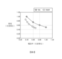
圖3為示出構成圖2的位元線電極層的材料與腐蝕程度之間的關係的曲線圖。 FIG. 3 is a graph showing the relationship between the material constituting the bit line electrode layer of FIG. 2 and the degree of corrosion.
圖4為繪示根據本發明概念的實施例的積體電路裝置的主要組態的橫截面圖。 4 is a cross-sectional view illustrating a main configuration of an integrated circuit device according to an embodiment of the inventive concept.
圖5為繪示根據本發明概念的實施例的積體電路裝置的主要組態的橫截面圖。 5 is a cross-sectional view illustrating a main configuration of an integrated circuit device according to an embodiment of the inventive concept.
圖6為示出構成圖5的位元線電極層的材料與特定電阻之間的關係的曲線圖。 FIG. 6 is a graph showing the relationship between materials constituting the bit line electrode layer of FIG. 5 and specific resistance.
圖7至圖14為根據製程序列來製造根據本發明概念的實施例的積體電路裝置的方法的橫截面圖。 7 to 14 are cross-sectional views of a method of manufacturing an integrated circuit device according to an embodiment of the inventive concept according to a fabrication sequence.
圖15為示出包含根據本發明概念的實施例的積體電路裝置的系統的方塊圖。 15 is a block diagram illustrating a system including an integrated circuit device according to an embodiment of the inventive concept.
在術語「約」或「實質上」在本說明書中結合數值使用時,相關聯數值意欲包含所陳述數值周圍的製造或操作容限(例如,±10%)。此外,當字組「通常」及「實質上」與幾何形狀結合使用時,意欲不要求幾何形狀的精確度,但形狀的寬容度在本揭露的範疇內。此外,不管數值或形狀是否經修改為「約」或「實質上」,應理解,此等值及形狀應解釋為包含所陳述數值或形狀周圍的製造或操作容限(例如±10%)。 When the terms "about" or "substantially" are used in connection with a numerical value in this specification, the associated numerical value is intended to include manufacturing or operating tolerances (eg, ±10%) around the stated value. Furthermore, when the words "usually" and "substantially" are used in conjunction with geometric shapes, it is intended that the precision of the geometric shapes is not required, but that the latitude of the shapes is within the scope of this disclosure. Furthermore, regardless of whether a value or shape is modified to mean "about" or "substantially," it is understood that such values and shapes should be interpreted to include manufacturing or operating tolerances (e.g., ±10%) around the stated value or shape.
在下文中,將參考隨附圖式詳細地描述本發明概念的實施例。 Hereinafter, embodiments of the inventive concept will be described in detail with reference to the accompanying drawings.
圖1為繪示根據本發明概念的實施例的積體電路裝置的主要組態的平面圖,圖2為繪示沿著圖1的線A-A'及線B-B'截取的主要組態的橫截面圖,且圖3為示出構成圖2的位元線電極層的材料與腐蝕程度之間的關係的曲線圖。 1 is a plan view illustrating a main configuration of an integrated circuit device according to an embodiment of the inventive concept, and FIG. 2 is a main configuration taken along lines AA' and BB' of FIG. 1 3 is a graph showing the relationship between the material constituting the bit line electrode layer of FIG. 2 and the degree of corrosion.
一起參考圖1至圖3,積體電路裝置100包含基底110,所述基底110具有由裝置隔離膜112界定的多個主動區域AC,以及跨多個主動區域AC延伸的多個閘極溝渠GT。
Referring to FIGS. 1-3 together, an
基底110可為包含矽(Si)的晶圓。在一些實施例中,基底110可為包含諸如鍺(Ge)的半導體元素,或諸如碳化矽(SiC)、砷化鎵(GaAs)、砷化銦(InAs)或磷化銦(InP)的化合物半導體的晶圓。此外,基底110可具有絕緣體上矽(silicon on insulator;SOI)結構。另外,基底110可包含導電區域,例如,摻雜有雜質的井,或摻雜有雜質的結構。 The substrate 110 may be a wafer including silicon (Si). In some embodiments, the substrate 110 may include a semiconductor element such as germanium (Ge), or a compound such as silicon carbide (SiC), gallium arsenide (GaAs), indium arsenide (InAs), or indium phosphide (InP). Semiconductor wafers. In addition, the substrate 110 may have a silicon on insulator (SOI) structure. Additionally, the substrate 110 may include conductive regions, such as wells doped with impurities, or structures doped with impurities.
多個主動區域AC可在X及Y方向上遠離彼此重複地形成,且可具有在傾斜方向上延伸以在不同於X方向及Y方向兩者 的一個方向(Q方向)上具有長軸的形狀。多個閘極溝渠GT可具有在X方向上彼此平行延伸的多個線形狀。 The plurality of active areas AC may be repeatedly formed away from each other in the X and Y directions, and may have extensions in the oblique direction to be different from both the has a long axis in one direction (Q direction). The plurality of gate trenches GT may have a plurality of line shapes extending parallel to each other in the X direction.
裝置隔離膜112可經配置以界定基底110中的多個主動區域AC。裝置隔離膜112可包含氧化矽膜、氮化矽膜或其組合。裝置隔離膜112可在X方向上在基底110上延伸且可在Y方向上彼此遠離。 Device isolation film 112 may be configured to define multiple active areas AC in substrate 110 . The device isolation film 112 may include a silicon oxide film, a silicon nitride film, or a combination thereof. The device isolation films 112 may extend over the substrate 110 in the X direction and may be separated from each other in the Y direction.
閘極介電膜120可形成於多個閘極溝渠GT中的各者中,填充閘極溝渠GT的一部分的閘極電極130可形成於閘極介電層120上,覆蓋閘極電極130的閘極保護膜140可形成於閘極溝渠GT中,且閘極保護膜140上的閘極頂蓋膜150可形成於閘極溝渠GT中。其中,閘極電極130及閘極保護膜140可構成閘極結構GS。 A gate dielectric film 120 may be formed in each of the plurality of gate trenches GT, and a gate electrode 130 filling a portion of the gate trenches GT may be formed on the gate dielectric layer 120 to cover a portion of the gate electrode 130 The gate protection film 140 may be formed in the gate trench GT, and the gate cap film 150 on the gate protection film 140 may be formed in the gate trench GT. Among them, the gate electrode 130 and the gate protective film 140 may constitute the gate structure GS.
基底110自閘極溝渠GT的底部暴露的部分的層級可高於裝置隔離膜112經暴露的部分的層級。因此,閘極結構GS的底部表面可具有對應於多個閘極溝渠GT的底部輪廓的凹凸形狀。因此,鞍鰭場效電晶體(fin field-effect transistor;FinFET)可形成於多個主動區域AC中。 The portion of the substrate 110 exposed from the bottom of the gate trench GT may be at a higher level than the exposed portion of the device isolation film 112 . Therefore, the bottom surface of the gate structure GS may have a concave and convex shape corresponding to the bottom contours of the plurality of gate trenches GT. Therefore, saddle-fin field-effect transistor (FinFET) can be formed in multiple active regions AC.
閘極介電膜120覆蓋閘極溝渠GT的內部表面,以便與主動區域AC及裝置隔離膜112接觸。閘極介電膜120可包含氧化矽膜、氮化矽膜、氮氧化矽膜、氧化物/氮化物/氧化物(oxide/nitride/oxide;ONO)膜,或具有比氧化矽膜的介電常數更高的介電常數的高k介電膜。高k介電膜可具有約10至25的介電常數,且可包含HfO2、Al2O3、HfAlO3、Ta2O3或TiO2。 The gate dielectric film 120 covers the inner surface of the gate trench GT so as to be in contact with the active area AC and the device isolation film 112 . The gate dielectric film 120 may include a silicon oxide film, a silicon nitride film, a silicon oxynitride film, an oxide/nitride/oxide (ONO; ONO) film, or a dielectric film having a higher density than a silicon oxide film. High-k dielectric films with higher constant dielectric constants. The high-k dielectric film may have a dielectric constant of about 10 to 25, and may include HfO 2 , Al 2 O 3 , HfAlO 3 , Ta 2 O 3 or TiO 2 .
閘極電極130可由金屬、金屬氮化物、金屬碳化物或其 組合形成。在一些實施例中,閘極電極130可由Ti、TiN、Ta、TaN、W、WN、TiSiN、WSiN或其組合形成。 The gate electrode 130 may be made of metal, metal nitride, metal carbide or other combination formed. In some embodiments, gate electrode 130 may be formed of Ti, TiN, Ta, TaN, W, WN, TiSiN, WSiN, or combinations thereof.
閘極保護膜140可配置於閘極電極130上。特定而言,閘極保護膜140配置於閘極電極130與閘極頂蓋膜150之間。閘極保護膜140可限制及/或防止構成閘極電極130及閘極頂蓋膜150兩者的不同材料的相互擴散或反應。閘極保護膜140可由例如多晶矽製成。 The gate protection film 140 may be disposed on the gate electrode 130 . Specifically, the gate protection film 140 is disposed between the gate electrode 130 and the gate top cover film 150 . The gate protection film 140 may limit and/or prevent interdiffusion or reaction of different materials constituting both the gate electrode 130 and the gate capping film 150 . The gate protection film 140 may be made of polysilicon, for example.
閘極頂蓋膜150填充閘極溝渠GT的內部以便與閘極介電膜120接觸。閘極頂蓋膜150可包含氮化矽膜、氮氧化矽膜或其組合。亦即,閘極頂蓋膜150可由與閘極介電膜120的材料不同的材料形成。 The gate cap film 150 fills the inside of the gate trench GT so as to be in contact with the gate dielectric film 120 . The gate cap film 150 may include a silicon nitride film, a silicon oxynitride film, or a combination thereof. That is, the gate cap film 150 may be formed of a different material from that of the gate dielectric film 120 .
閘極結構GS具有面向主動區域AC的閘極側壁,且閘極頂蓋膜150包含面向主動區域AC的絕緣側壁部分。源極/汲極區域SD可形成於多個主動區域AC中的閘極結構GS的兩側上。 The gate structure GS has a gate sidewall facing the active area AC, and the gate top cap film 150 includes an insulating sidewall portion facing the active area AC. Source/drain regions SD may be formed on both sides of the gate structure GS in the plurality of active regions AC.
多個閘極結構GS可構成多個字元線。亦即,多個字元線可跨多個主動區域AC在X方向上彼此平行地延伸。多個位元線BL可在Y方向上在多個字元線上彼此平行地延伸。多個位元線BL可經由直接觸點DC連接至多個主動區域AC。 Multiple gate structures GS can form multiple word lines. That is, the plurality of word lines may extend parallel to each other in the X direction across the plurality of active areas AC. The plurality of bit lines BL may extend parallel to each other on the plurality of word lines in the Y direction. A plurality of bit lines BL may be connected to a plurality of active areas AC via direct contacts DC.
層間絕緣膜210可包含依序形成於基底110上的第一層間絕緣膜212及第二層間絕緣膜214。第一層間絕緣膜212及第二層間絕緣膜214可由不同類型的絕緣材料製成。舉例而言,第一層間絕緣膜212可包含氧化矽膜,且第二層間絕緣膜214可包含氮化矽膜,但本發明概念不限於此。 The interlayer insulating film 210 may include a first interlayer insulating film 212 and a second interlayer insulating film 214 sequentially formed on the substrate 110 . The first interlayer insulating film 212 and the second interlayer insulating film 214 may be made of different types of insulating materials. For example, the first interlayer insulating film 212 may include a silicon oxide film, and the second interlayer insulating film 214 may include a silicon nitride film, but the inventive concept is not limited thereto.
層間導電膜220可由摻雜多晶矽製成。另外,直接觸點 DC可由摻雜多晶矽形成。在一些實施例中,層間導電膜220及直接觸點DC可由具有不同摻雜濃度的多晶矽形成。 The interlayer conductive film 220 may be made of doped polycrystalline silicon. Additionally, direct contact DC can be formed from doped polycrystalline silicon. In some embodiments, the interlayer conductive film 220 and the direct contact DC may be formed of polycrystalline silicon with different doping concentrations.
直接觸點DC可形成為填充直接接觸孔DCH的內部。藉由蝕刻層間絕緣膜210及層間導電膜220的部分區域及基底110的部分區域來形成直接接觸孔DCH,使得直接接觸孔DCH可形成為穿透層間絕緣膜210及層間導電膜220以暴露主動區域AC。 The direct contact DC may be formed to fill the interior of the direct contact hole DCH. The direct contact hole DCH is formed by etching part of the interlayer insulating film 210 and the interlayer conductive film 220 and part of the substrate 110 so that the direct contact hole DCH can be formed to penetrate the interlayer insulating film 210 and the interlayer conductive film 220 to expose the active layer. Area AC.
位元線矽化物層(未繪示)及位元線障壁層230可依序包含於層間導電膜220上。位元線矽化物層(未繪示)可由金屬矽化物形成。位元線障壁層230可由TiSiN、TiN、TaN、CoN、金屬、金屬矽化物或其組合形成。金屬及金屬矽化物可包含W、Mo、Au、Cu、Al、Ni或Co,但本發明概念不限於此。 A bit line silicon layer (not shown) and a bit line barrier layer 230 may be sequentially included on the interlayer conductive film 220. The bit line silicon layer (not shown) may be formed of metal silicon. The bit line barrier layer 230 may be formed of TiSiN, TiN, TaN, CoN, metal, metal silicide, or combinations thereof. The metal and metal silicide may include W, Mo, Au, Cu, Al, Ni or Co, but the inventive concept is not limited thereto.
在本發明概念的積體電路裝置100中,非晶金屬層240及晶種層250可依序包含於位元線障壁層230上。非晶金屬層240及晶種層250可為額外材料層以有效地生長構成稍後將描述的位元線電極層260的金屬材料。在一些實施例中,可省略非晶金屬層240及晶種層250。
In the
非晶金屬層240可為自以下中選出的任一者:WBx、MoBx、MoWBx、TaBx、NbBx、HfBx、ZrBx以及CoBx。為了有效地控制安置於非晶金屬層240上的晶種層250的定向及粒度,可使非晶金屬層240形成有約0.5奈米至約5奈米的厚度。 The amorphous metal layer 240 may be any one selected from: WBx , MoBx , MoWBx , TaBx , NbBx , HfBx , ZrBx , and CoBx . In order to effectively control the orientation and particle size of the seed layer 250 disposed on the amorphous metal layer 240, the amorphous metal layer 240 may be formed to have a thickness of about 0.5 nm to about 5 nm.
另外,晶種層250可為自以下中選出的任一者:Mo、W、MoW、MoTa以及MoWTa。為了有效地控制安置於晶種層250上的位元線電極層260的定向及粒度,可使晶種層250形成有約1奈米至約10奈米的厚度。 In addition, the seed layer 250 may be any one selected from the following: Mo, W, MoW, MoTa, and MoWTa. In order to effectively control the orientation and granularity of the bit line electrode layer 260 disposed on the seed layer 250, the seed layer 250 may be formed to have a thickness of about 1 nm to about 10 nm.
在本發明概念的積體電路裝置100中,位元線電極層260安置於晶種層250上。作為用於形成位元線電極層260的材料,可使用作為二進位完美固體溶液(binary perfect solid solution)的鉬鎢(MoW)合金。此處,位元線障壁層230、非晶金屬層240、晶種層250以及位元線電極層260可構成位元線BL。
In the
特定而言,在鉬(Mo)及鎢(W)的合金化製程期間,鉬鎢(MoW)合金為能夠在所有組分中形成合金的完美固體溶液,且繪示各材料的電阻率的平均值總和與各組分成比例。另外,在形成MoW合金的製程中,由於可控制具有相對較高特定電阻的β W的生長,因此MoW合金具有易於確保低特定電阻的特性。另外,MoW合金具有以下性質:耐腐蝕性比各材料的耐腐蝕性提高約4倍至20倍。 Specifically, during the alloying process of molybdenum (Mo) and tungsten (W), the molybdenum tungsten (MoW) alloy is a perfect solid solution capable of forming alloys in all components, and the average resistivity of each material is plotted The sum of values is proportional to each component. In addition, in the process of forming the MoW alloy, since the growth of β W with relatively high specific resistance can be controlled, the MoW alloy has characteristics that make it easy to ensure low specific resistance. In addition, MoW alloy has the following properties: corrosion resistance is approximately 4 to 20 times higher than that of each material.
如圖3中所繪示,在滿足以上特性的同時,特別地,MoW合金的組成比可用於耐腐蝕性強的合金部分中。亦即,用於位元線電極層260的MoW合金可經形成以包含約25原子%至約75原子%的Mo。另外,考慮到金屬佈線的電阻、電容以及製程難度,用作位元線電極層260的MoW合金的厚度可在約10奈米至約30奈米的範圍內調整。稍後將描述製造此MoW合金的方法的細節。 As shown in FIG. 3 , while satisfying the above characteristics, in particular, the composition ratio of the MoW alloy can be used in an alloy part with strong corrosion resistance. That is, the MoW alloy used for the bit line electrode layer 260 may be formed to include about 25 atomic % to about 75 atomic % Mo. In addition, considering the resistance, capacitance and process difficulty of metal wiring, the thickness of the MoW alloy used as the bit line electrode layer 260 can be adjusted in the range of about 10 nanometers to about 30 nanometers. Details of the method of making this MoW alloy will be described later.
位元線頂蓋層270可包含依序形成於位元線電極層260上的第一位元線頂蓋層272及第二位元線頂蓋層274。在一些實施例中,第一位元線頂蓋層272及第二位元線頂蓋層274可由相同類型的絕緣材料形成。舉例而言,第一位元線頂蓋層272及第二位元線頂蓋層274可包含氮化矽層。在其他實施例中,第一位元線頂蓋層272及第二位元線頂蓋層274可由不同類型的絕緣材料 形成。舉例而言,第一位元線頂蓋層272可包含氧化矽膜,且第二位元線頂蓋層274可包含氮化矽膜。 The bit line cap layer 270 may include a first bit line cap layer 272 and a second bit line cap layer 274 sequentially formed on the bit line electrode layer 260 . In some embodiments, the first bit line cap layer 272 and the second bit line cap layer 274 may be formed of the same type of insulating material. For example, the first bit line cap layer 272 and the second bit line cap layer 274 may include silicon nitride layers. In other embodiments, the first bit line cap layer 272 and the second bit line cap layer 274 may be made of different types of insulating materials. form. For example, the first bit line cap layer 272 may include a silicon oxide film, and the second bit line cap layer 274 may include a silicon nitride film.
近來,隨著積體電路裝置100的設計規則快速減少,金屬佈線的線寬亦快速減小。因此,與經由未圖案化晶圓的電阻率量測預測的金屬佈線的第一電阻率相比,在利用精細線寬進行圖案化之後量測的金屬佈線的第二電阻率大得多。隨著金屬佈線的線寬急劇減小,除增加在金屬蝕刻製程期間形成的損壞層自身的電阻率以外,由表面損壞引起的表面散射效應加速,且分析出金屬佈線的電阻快速增加。
Recently, as the design rules of the
特定而言,隨著位元線BL的線寬減小,易受用作習知金屬佈線的W的腐蝕環境影響的特性(例如,氧化)經分析為電阻快速增加的原因。因此,在形成位元線BL的過程中,需要具有低電阻及耐腐蝕性的材料以替代W。另外,隨著位元線BL的長度急劇減小,可能需要具有較短電子平均自由路徑及簡易的蝕刻製程的材料。 Specifically, as the line width of the bit line BL decreases, characteristics (for example, oxidation) susceptible to the corrosive environment of W used as conventional metal wiring are analyzed to be the cause of the rapid increase in resistance. Therefore, in the process of forming the bit line BL, a material with low resistance and corrosion resistance is required to replace W. In addition, as the length of the bit line BL decreases sharply, materials with a shorter electron mean free path and a simple etching process may be required.
在本發明概念的積體電路裝置100中,藉由將MoW合金(其為滿足以上要求的材料)應用於位元線電極層260,所述位元線電極層260具有能夠實現電特性、製程容易度以及價格競爭力的效應。因此,在本發明概念的實施例中,MoW合金在積體電路裝置100的超精細金屬佈線製程中作為構成位元線BL的材料而應用,使得有可能限制及/或防止由在W單金屬中發生腐蝕引起的快速電阻增加。
In the
最終,根據本發明概念,在包含埋入式通道陣列電晶體的積體電路裝置100中,藉由使用MoW合金作為構成位元線電極
層260的金屬材料,存在改良電特性及產品可靠度的效應。
Finally, according to the concept of the present invention, in the
圖4為繪示根據本發明概念的實施例的積體電路裝置的主要組態的橫截面圖。圖4中的橫截面圖可沿著圖1的線A-A'及線B-B'截取。 4 is a cross-sectional view illustrating a main configuration of an integrated circuit device according to an embodiment of the inventive concept. The cross-sectional view in FIG. 4 may be taken along lines AA′ and BB′ of FIG. 1 .
構成下文所描述的積體電路裝置100A的大部分組件及構成所述組件的材料與上文參考圖1至圖3所描述的組件及材料實質上相同或類似。因此,為方便描述起見,描述將集中於與上文所描述的積體電路裝置100的差異。
Most of the components constituting the integrated circuit device 100A described below and the materials constituting the components are substantially the same or similar to the components and materials described above with reference to FIGS. 1 to 3 . Therefore, for convenience of description, the description will focus on the differences from the
參考圖4,積體電路裝置100A的單元陣列區域可包含多個主動區域AC。多個位元線BL可在Y方向上彼此平行地延伸。多個位元線BL可經由直接觸點DCA分別連接至多個主動區域AC。 Referring to FIG. 4 , the cell array area of the integrated circuit device 100A may include a plurality of active areas AC. The plurality of bit lines BL may extend parallel to each other in the Y direction. The plurality of bit lines BL may be respectively connected to the plurality of active areas AC via direct contacts DCA.
在此實施例的積體電路裝置100A中,直接觸點DCA可由金屬材料製成,且金屬材料可為自以下中選出的任一者:Mo、W、MoW以及TiN。直接觸點DCA可形成為填充直接接觸孔DCH的內部。藉由蝕刻層間絕緣膜310及層間導電膜320的部分區域及基底110的部分區域來形成直接接觸孔DCH,使得直接接觸孔DCH可形成為穿透層間絕緣膜310及層間導電膜320以暴露主動區域AC。 In the integrated circuit device 100A of this embodiment, the direct contact DCA may be made of a metal material, and the metal material may be any one selected from the following: Mo, W, MoW, and TiN. The direct contact DCA may be formed to fill the inside of the direct contact hole DCH. The direct contact hole DCH is formed by etching part of the interlayer insulating film 310 and the interlayer conductive film 320 and part of the substrate 110 so that the direct contact hole DCH can be formed to penetrate the interlayer insulating film 310 and the interlayer conductive film 320 to expose the active layer. Area AC.
在本實施例的積體電路裝置100A中,接觸障壁層332及接觸矽化物層334可進一步形成於基底110與直接觸點DCA之間。接觸障壁層332可由TiSiN、TiN、TaN、CoN、金屬、金屬矽化物或其組合形成。金屬及金屬矽化物可包含W、Mo、Au、Cu、Al、Ni或Co。另外,接觸矽化物層334可由矽化W、矽化Mo或 矽化鈦(Ti)形成,但不限於此。 In the integrated circuit device 100A of this embodiment, the contact barrier layer 332 and the contact silicide layer 334 may be further formed between the substrate 110 and the direct contact DCA. The contact barrier layer 332 may be formed of TiSiN, TiN, TaN, CoN, metal, metal silicide, or combinations thereof. Metals and metal silicides may include W, Mo, Au, Cu, Al, Ni or Co. In addition, the contact silicide layer 334 may be made of W silicide, Mo silicide, or Titanium silicide (Ti) is formed, but is not limited thereto.
在本發明概念的積體電路裝置100A中,位元線接合層340及晶種層350可依序包含於層間導電膜320上。位元線接合層340及晶種層350可為額外材料層以有效地生長構成位元線電極層360的金屬材料。在一些實施例中,可省略晶種層350。 In the integrated circuit device 100A of the present invention, the bit line bonding layer 340 and the seed layer 350 may be sequentially included on the interlayer conductive film 320. The bit line bonding layer 340 and the seed layer 350 may be additional material layers to effectively grow the metal material constituting the bit line electrode layer 360. In some embodiments, seed layer 350 may be omitted.
在本實施例的積體電路裝置100A中,位元線電極層360安置於晶種層350上。作為用於形成位元線電極層360的材料,可使用作為二進位完美固體溶液的MoW合金。位元線頂蓋層370可包含依序形成於位元線電極層360上的第一位元線頂蓋層372及第二位元線頂蓋層374。此處,位元線接合層340、晶種層350以及位元線電極層360可構成位元線BL。 In the integrated circuit device 100A of this embodiment, the bit line electrode layer 360 is disposed on the seed layer 350 . As a material for forming the bit line electrode layer 360, MoW alloy which is a binary perfect solid solution can be used. The bit line cap layer 370 may include a first bit line cap layer 372 and a second bit line cap layer 374 sequentially formed on the bit line electrode layer 360. Here, the bit line bonding layer 340, the seed layer 350 and the bit line electrode layer 360 may constitute the bit line BL.
圖5為繪示根據本發明概念的實施例的積體電路裝置的主要組態的橫截面圖,且圖6為示出構成圖5的位元線電極層的材料與特定電阻之間的關係的曲線圖。圖5中的橫截面圖可沿著圖1的線A-A'及線B-B'截取。 5 is a cross-sectional view illustrating a main configuration of an integrated circuit device according to an embodiment of the inventive concept, and FIG. 6 is a diagram illustrating the relationship between materials constituting the bit line electrode layer of FIG. 5 and a specific resistance. curve graph. The cross-sectional view in FIG. 5 may be taken along line AA' and line BB' of FIG. 1 .
構成下文所描述的積體電路裝置100B的大部分組件及構成所述組件的材料與上文參考圖1至圖3所描述的所述組件及材料實質上相同或類似。因此,為方便描述起見,描述將集中於與上文所描述的積體電路裝置100的差異。
Most of the components and materials constituting the integrated circuit device 100B described below are substantially the same or similar to the components and materials described above with reference to FIGS. 1 to 3 . Therefore, for convenience of description, the description will focus on the differences from the
一起參考圖5及圖6,積體電路裝置100B的單元陣列區域可包含多個主動區域AC。多個位元線BL可在Y方向上彼此平行地延伸。多個位元線BL可經由直接觸點DC連接至多個主動區域AC。 Referring to FIGS. 5 and 6 together, the cell array area of the integrated circuit device 100B may include a plurality of active areas AC. The plurality of bit lines BL may extend parallel to each other in the Y direction. A plurality of bit lines BL may be connected to a plurality of active areas AC via direct contacts DC.
在本實施例的積體電路裝置100B中,非晶金屬層240可 位於位元線障壁層230上。非晶金屬層240可為額外材料層以有效地生長構成位元線電極層460的金屬材料。在一些實施例中,可省略非晶金屬層240。 In the integrated circuit device 100B of this embodiment, the amorphous metal layer 240 may Located on the bit line barrier layer 230. The amorphous metal layer 240 may be an additional material layer to effectively grow the metal material constituting the bit line electrode layer 460 . In some embodiments, amorphous metal layer 240 may be omitted.
在本實施例的積體電路裝置100B中,位元線電極層460安置於非晶金屬層240上。MoW合金可用作用於形成位元線電極層460的材料。特定而言,用於位元線電極層460的MoW合金可為包含交替安置的多個鉬層461及多個鎢層462的超晶格合金。在MoW超晶格合金中,Mo可佔約25原子%至約75原子%。此處,位元線障壁層230、非晶金屬層240以及位元線電極層460可構成位元線BL。 In the integrated circuit device 100B of this embodiment, the bit line electrode layer 460 is disposed on the amorphous metal layer 240 . MoW alloy may be used as a material for forming the bit line electrode layer 460 . Specifically, the MoW alloy used for the bit line electrode layer 460 may be a superlattice alloy including a plurality of molybdenum layers 461 and a plurality of tungsten layers 462 arranged alternately. In MoW superlattice alloys, Mo may account for about 25 atomic % to about 75 atomic %. Here, the bit line barrier layer 230, the amorphous metal layer 240 and the bit line electrode layer 460 may constitute the bit line BL.
在此實施例的積體電路裝置100B中,多個鉬層461與多個鎢層462當中的最下層(第一層)可具有約0.5奈米至約10奈米的厚度。相比而言,多個鉬層461及多個鎢層462當中的不包含最下層(第一層)的剩餘層可各自具有約0.5埃至約10埃的厚度。亦即,最下層(第一層)可充當用於增加位元線電極層460的定向及粒度的晶種層。 In the integrated circuit device 100B of this embodiment, the lowermost layer (the first layer) among the plurality of molybdenum layers 461 and the plurality of tungsten layers 462 may have a thickness of about 0.5 nanometers to about 10 nanometers. In comparison, remaining layers excluding the lowermost layer (first layer) among the plurality of molybdenum layers 461 and the plurality of tungsten layers 462 may each have a thickness of about 0.5 angstroms to about 10 angstroms. That is, the lowermost layer (the first layer) may serve as a seed layer for increasing the orientation and granularity of the bit line electrode layer 460 .
如在圖6中,當位元線電極層460由MoW超晶格合金製成時,由於最下層(第一層)的形成可限制及/或抑制具有相對較高電阻率的β W的形成,因此可確保比單層(例如,單一鉬層)更低的電阻率。另外,當位元線電極層460由MoW超晶格合金製成時,可確保相對均勻的粒度及組成分佈,且因此耐腐蝕性可為極佳的。 As in FIG. 6 , when the bit line electrode layer 460 is made of MoW superlattice alloy, the formation of the lowermost layer (first layer) can limit and/or inhibit the formation of β W with relatively high resistivity. , thus ensuring lower resistivity than a single layer (for example, a single molybdenum layer). In addition, when the bit line electrode layer 460 is made of MoW superlattice alloy, relatively uniform particle size and composition distribution can be ensured, and therefore corrosion resistance can be excellent.
圖7至圖14為根據製程序列來製造根據本發明概念的實施例的積體電路裝置的方法的橫截面圖。 7 to 14 are cross-sectional views of a method of manufacturing an integrated circuit device according to an embodiment of the inventive concept according to a fabrication sequence.
參考圖7,在基底110的單元陣列區域中形成多個裝置隔離溝渠TR之後,形成填充多個裝置隔離溝渠TR的多個裝置隔離膜112。多個主動區域AC可由多個裝置隔離膜112界定於基底110的單元陣列區域中。 Referring to FIG. 7 , after a plurality of device isolation trenches TR are formed in the cell array region of the substrate 110 , a plurality of device isolation films 112 filling the plurality of device isolation trenches TR are formed. A plurality of active areas AC may be defined by a plurality of device isolation films 112 in the cell array area of the substrate 110 .
基底110可為包含矽(Si)的晶圓。在一些實施例中,基底110可為包含諸如鍺(Ge)的半導體元素,或諸如碳化矽(SiC)、砷化鎵(GaAs)、砷化銦(InAs)或磷化銦(InP)的化合物半導體的晶圓。 The substrate 110 may be a wafer including silicon (Si). In some embodiments, the substrate 110 may include a semiconductor element such as germanium (Ge), or a compound such as silicon carbide (SiC), gallium arsenide (GaAs), indium arsenide (InAs), or indium phosphide (InP). Semiconductor wafers.
在藉由將雜質離子植入至多個主動區域AC的上部表面中來形成多個源極/汲極區域之後,在基底110中形成彼此平行地延伸的多個閘極溝渠GT。在清洗包含多個閘極溝渠GT的所得結構之後,接下來,在多個閘極溝渠GT中的各者中形成閘極介電層120、閘極結構GS以及閘極頂蓋膜150。多個閘極結構GS可構成多個字元線。 After forming a plurality of source/drain regions by implanting impurity ions into upper surfaces of a plurality of active regions AC, a plurality of gate trenches GT extending parallel to each other are formed in the substrate 110 . After cleaning the resulting structure including the plurality of gate trenches GT, next, the gate dielectric layer 120, the gate structure GS, and the gate capping film 150 are formed in each of the plurality of gate trenches GT. Multiple gate structures GS can form multiple word lines.
閘極結構GS可包含閘極電極130及閘極保護膜140。閘極電極130可由金屬、金屬氮化物、金屬碳化物或其組合形成。閘極保護膜140可形成於閘極電極130上。特定而言,閘極保護膜140可形成於閘極電極130與閘極頂蓋膜150之間。 The gate structure GS may include a gate electrode 130 and a gate protection film 140 . Gate electrode 130 may be formed of metal, metal nitride, metal carbide, or combinations thereof. The gate protection film 140 may be formed on the gate electrode 130 . Specifically, the gate protection film 140 may be formed between the gate electrode 130 and the gate top cap film 150 .
接下來,可在基底110上形成層間絕緣膜210。層間絕緣膜210可包含依序形成於基底110上的第一層間絕緣膜212及第二層間絕緣膜214。第一層間絕緣膜212及第二層間絕緣膜214可由不同類型的絕緣材料製成。舉例而言,第一層間絕緣膜212可包含氧化矽膜,且第二層間絕緣膜214可包含氮化矽膜,但本發明概念不限於此。 Next, an interlayer insulating film 210 may be formed on the substrate 110 . The interlayer insulating film 210 may include a first interlayer insulating film 212 and a second interlayer insulating film 214 sequentially formed on the substrate 110 . The first interlayer insulating film 212 and the second interlayer insulating film 214 may be made of different types of insulating materials. For example, the first interlayer insulating film 212 may include a silicon oxide film, and the second interlayer insulating film 214 may include a silicon nitride film, but the inventive concept is not limited thereto.
參考圖8,在於基底110上形成層間導電膜220之後,藉由蝕刻層間絕緣膜210及層間導電膜220的部分區域及基底110的部分區域,多個直接接觸孔DCH可形成穿過層間絕緣膜210及層間導電膜220形成以暴露主動區域AC。 Referring to FIG. 8 , after the interlayer conductive film 220 is formed on the substrate 110 , by etching the interlayer insulating film 210 and a partial area of the interlayer conductive film 220 and a partial area of the substrate 110 , a plurality of direct contact holes DCH can be formed through the interlayer insulating film. 210 and an interlayer conductive film 220 are formed to expose the active area AC.
層間導電膜220可由摻雜多晶矽或金屬,諸如W、Mo、Au、Cu、Al、Ni或Co製成。層間導電膜220可包含由自以上實例材料中選出的一種材料製成的單層,或由多種材料製成的多層。 The interlayer conductive film 220 may be made of doped polycrystalline silicon or metal such as W, Mo, Au, Cu, Al, Ni, or Co. The interlayer conductive film 220 may include a single layer made of one material selected from the above example materials, or multiple layers made of multiple materials.
多個直接觸點DC可形成為分別填充多個直接接觸孔DCH。多個直接觸點DC可由摻雜多晶矽形成。在一些實施例中,多個直接觸點DC可由實質上相同的材料形成,但直接觸點DC的摻雜濃度與層間導電膜220的摻雜濃度不同。 A plurality of direct contacts DC may be formed to fill a plurality of direct contact holes DCH respectively. Multiple direct contacts DC may be formed from doped polysilicon. In some embodiments, the plurality of direct contacts DC may be formed of substantially the same material, but the doping concentration of the direct contacts DC is different from that of the interlayer conductive film 220 .
參考圖9,在層間導電膜220上依序形成位元線矽化物層(未繪示)、位元線障壁層230、非晶金屬層240以及晶種層250。 Referring to FIG. 9 , a bit line silicide layer (not shown), a bit line barrier layer 230 , an amorphous metal layer 240 and a seed layer 250 are sequentially formed on the interlayer conductive film 220 .
位元線矽化物層(未繪示)可由金屬矽化物形成。此外,位元線障壁層230可由TiSiN、TiN、TaN、CoN、金屬、金屬矽化物或其組合形成。金屬及金屬矽化物可包含W、Mo、Au、Cu、Al、Ni或Co,但本發明概念不限於此。 The bit line silicon layer (not shown) may be formed of metal silicon. In addition, the bit line barrier layer 230 may be formed of TiSiN, TiN, TaN, CoN, metal, metal silicide, or combinations thereof. The metal and metal silicide may include W, Mo, Au, Cu, Al, Ni or Co, but the inventive concept is not limited thereto.
接下來,位元線障壁層230上可依序包含非晶金屬層240及晶種層250。非晶金屬層240及晶種層250可為額外材料層以有效地生長構成位元線電極層260的金屬材料。在一些實施例中,可省略非晶金屬層240及晶種層250。 Next, the bit line barrier layer 230 may include an amorphous metal layer 240 and a seed layer 250 in sequence. The amorphous metal layer 240 and the seed layer 250 may be additional material layers to effectively grow the metal material constituting the bit line electrode layer 260 . In some embodiments, the amorphous metal layer 240 and the seed layer 250 may be omitted.
非晶金屬層240可為自以下中選出的任一者:WBx、MoBx、MoWBx、TaBx、NbBx、HfBx、ZrBx以及CoBx。為了有效地控制安置於非晶金屬層240上的晶種層250的定向及粒度,可 使非晶金屬層240形成有約0.5奈米至約5奈米的厚度。 The amorphous metal layer 240 may be any one selected from: WBx , MoBx , MoWBx , TaBx , NbBx , HfBx , ZrBx , and CoBx . In order to effectively control the orientation and particle size of the seed layer 250 disposed on the amorphous metal layer 240, the amorphous metal layer 240 may be formed to have a thickness of about 0.5 nm to about 5 nm.
晶種層250可為自以下中選出的任一者:Mo、W、MoW、MoTa以及MoWTa。為了有效地控制安置於晶種層250上的位元線電極層260的定向及粒度,可使晶種層250形成有約1奈米至約10奈米的厚度。 The seed layer 250 may be any one selected from the following: Mo, W, MoW, MoTa, and MoWTa. In order to effectively control the orientation and granularity of the bit line electrode layer 260 disposed on the seed layer 250, the seed layer 250 may be formed to have a thickness of about 1 nm to about 10 nm.
參考圖10,可使用MoW合金在晶種層250上形成位元線電極層260。 Referring to FIG. 10 , a MoW alloy may be used to form the bit line electrode layer 260 on the seed layer 250 .
位元線電極層260可由作為二進位完美固體溶液的MoW合金形成。MoW合金可藉由物理氣相沈積(physical vapor deposition;PVD)方法、化學氣相沈積(chemical vapor deposition;CVD)方法或原子層沈積(atomic layer deposition;ALD)方法形成,且可考慮到特定電阻特性、表面粗糙度、耐腐蝕性以及類似者而選擇性地使用。在一些實施例中,當藉由PVD方法形成位元線電極層260時,可在約200℃至約550℃範圍內的高溫下形成成形溫度以增加定向及粒度。在其他實施例中,當藉由VD方法或ALD方法形成位元線電極層260時,可在約200℃至約750℃範圍內的高溫下形成成形溫度以增加定向及粒度。 The bit line electrode layer 260 may be formed of MoW alloy which is a binary perfect solid solution. MoW alloy can be formed by physical vapor deposition (PVD) method, chemical vapor deposition (CVD) method or atomic layer deposition (ALD) method, and can take into account specific resistance properties, surface roughness, corrosion resistance and the like. In some embodiments, when bit line electrode layer 260 is formed by a PVD method, the forming temperature may be formed at a high temperature in the range of about 200°C to about 550°C to increase orientation and granularity. In other embodiments, when the bit line electrode layer 260 is formed by the VD method or the ALD method, the forming temperature may be formed at a high temperature in the range of about 200°C to about 750°C to increase orientation and granularity.
考慮到金屬佈線的電阻、電容以及製程困難,用作位元線電極層260的MoW合金的厚度可在約10奈米至約30奈米的範圍內調整。 Taking into account the resistance, capacitance and process difficulties of metal wiring, the thickness of the MoW alloy used as the bit line electrode layer 260 can be adjusted in the range of about 10 nanometers to about 30 nanometers.
在形成位元線電極層260之後,為了MoW合金的晶粒再生長或雜質移除,可在約400℃至約1200℃的範圍內執行惰性氣體或氫氣(H2)氣氛退火。 After the bit line electrode layer 260 is formed, inert gas or hydrogen (H 2 ) atmosphere annealing may be performed in a range of about 400°C to about 1200°C for grain regrowth or impurity removal of the MoW alloy.
儘管圖式中未繪示,但為了限制及/或防止MoW合金的 表面氧化及表面氮化,亦有可能在同一設施中形成MoW合金且形成原位頂蓋層。作為構成原位頂蓋層的材料,可使用石墨烯,所述石墨烯在高溫下穩定且在後續處理期間具有極佳的防污染保護。 Although not shown in the drawing, in order to limit and/or prevent the MoW alloy Surface oxidation and surface nitridation may also form MoW alloys and form an in-situ capping layer in the same facility. As the material constituting the in-situ capping layer, graphene can be used, which is stable at high temperatures and offers excellent protection against contamination during subsequent processing.
參考圖11,可在位元線電極層260上形成位元線頂蓋層270。 Referring to FIG. 11 , a bit line capping layer 270 may be formed on the bit line electrode layer 260 .
位元線頂蓋層270可包含依序形成於位元線電極層260上的第一位元線頂蓋層272及第二位元線頂蓋層274。第二位元線頂蓋層274可經形成以比第一位元線頂蓋層272更厚。 The bit line cap layer 270 may include a first bit line cap layer 272 and a second bit line cap layer 274 sequentially formed on the bit line electrode layer 260 . The second bit line cap layer 274 may be formed thicker than the first bit line cap layer 272 .
在一些實施例中,第一位元線頂蓋層272及第二位元線頂蓋層274可由相同類型的絕緣材料形成。舉例而言,第一位元線頂蓋層272及第二位元線頂蓋層274可包含氮化矽層。 In some embodiments, the first bit line cap layer 272 and the second bit line cap layer 274 may be formed of the same type of insulating material. For example, the first bit line cap layer 272 and the second bit line cap layer 274 may include silicon nitride layers.
在其他實施例中,第一位元線頂蓋層272及第二位元線頂蓋層274可由不同類型的絕緣材料形成。舉例而言,第一位元線頂蓋層272可包含氧化矽膜,且第二位元線頂蓋層274可包含氮化矽膜。 In other embodiments, the first bit line cap layer 272 and the second bit line cap layer 274 may be formed of different types of insulating materials. For example, the first bit line cap layer 272 may include a silicon oxide film, and the second bit line cap layer 274 may include a silicon nitride film.
因此,已描述根據本發明概念的實施例的積體電路裝置100的主要組態的製造製程。在下文中,將描述積體電路裝置100的後續製程。
Accordingly, the manufacturing process of the main configuration of the
參考圖12,可在位元線頂蓋層270上形成硬遮罩圖案280。可經由硬遮罩圖案280暴露位元線頂蓋層270的上部表面的一部分。硬遮罩圖案280可包含氮化矽膜。 Referring to FIG. 12 , a hard mask pattern 280 may be formed on the bit line capping layer 270 . A portion of the upper surface of bit line capping layer 270 may be exposed via hard mask pattern 280 . Hard mask pattern 280 may include a silicon nitride film.
藉由使用硬遮罩圖案280作為蝕刻遮罩來蝕刻包含直接觸點DC、層間絕緣膜、層間導電膜220、位元線障壁層230、非 晶金屬層240、晶種層250、位元線電極層260以及位元線頂蓋層270的堆疊結構,形成彼此平行地延伸的多個間隔開的結構。此處,位元線障壁層230、非晶金屬層240、晶種層250以及位元線電極層260可構成位元線BL。 By using the hard mask pattern 280 as an etching mask, the film including the direct contact DC, the interlayer insulating film, the interlayer conductive film 220, the bit line barrier layer 230, and the non-contact film are etched. The stacked structure of the crystal metal layer 240, the seed layer 250, the bit line electrode layer 260 and the bit line capping layer 270 forms a plurality of spaced apart structures extending parallel to each other. Here, the bit line barrier layer 230, the amorphous metal layer 240, the seed layer 250 and the bit line electrode layer 260 may constitute the bit line BL.
參考圖13,形成覆蓋多個位元線BL中的各者的兩個側壁的多個間隔件282,且蝕刻經由多個間隔件282暴露的基底110的一部分及裝置隔離膜112的一部分,以形成暴露多個主動區域AC的多個凹部RC。 Referring to FIG. 13 , a plurality of spacers 282 covering both sidewalls of each of the plurality of bit lines BL are formed, and a portion of the substrate 110 and a portion of the device isolation film 112 exposed through the plurality of spacers 282 are etched to A plurality of recesses RC are formed exposing a plurality of active areas AC.
多個凹部RC可與具有由鄰近位元線BL之間的一對間隔件282界定的寬度的埋入式接觸孔BCH連通。 The plurality of recesses RC may communicate with a buried contact hole BCH having a width defined by a pair of spacers 282 between adjacent bit lines BL.
為了形成多個間隔件282及多個凹部RC,形成用於形成覆蓋多個位元線BL的間隔件的絕緣膜,且可執行回蝕用於形成間隔件的絕緣膜的製程以及蝕刻基底110的一部分及裝置隔離膜112的一部分的製程。 In order to form the plurality of spacers 282 and the plurality of recesses RC, an insulating film for forming spacers covering the plurality of bit lines BL is formed, and a process of etching back the insulating film for forming the spacers and etching the substrate 110 may be performed and a process for installing a part of the isolation film 112 .
參考圖14,在填充多個位元線BL中的各者之間的多個凹部RC的同時,可形成依次堆疊於多個埋入式接觸孔BCH中的埋入式導電膜290、埋入式矽化物膜292、導電障壁膜294以及上部導電膜296。 Referring to FIG. 14 , while filling the plurality of recessed portions RC between each of the plurality of bit lines BL, the buried conductive films 290 and the buried conductive films 290 sequentially stacked in the plurality of buried contact holes BCH may be formed. A silicide film 292, a conductive barrier film 294, and an upper conductive film 296.
埋入式導電膜290、埋入式矽化物膜292、導電障壁膜294以及上部導電膜296可形成埋入式觸點BC。 The buried conductive film 290, the buried silicide film 292, the conductive barrier film 294, and the upper conductive film 296 may form a buried contact BC.
多個上部導電膜296的延伸部分可用作多個著陸墊,在後續製程中形成的電容器的下部電極(未繪示)可連接至所述著陸墊。 Extended portions of upper conductive films 296 may serve as landing pads to which lower electrodes (not shown) of capacitors formed in subsequent processes may be connected.
多個埋入式導電膜290可藉由CVD、PVD或磊晶生長製 程形成。多個埋入式導電膜290可由摻雜有雜質的半導體材料、金屬、導電金屬氮化物、金屬矽化物或其組合形成。 The plurality of buried conductive films 290 can be grown by CVD, PVD or epitaxial growth. process formed. The plurality of buried conductive films 290 may be formed of impurity-doped semiconductor materials, metals, conductive metal nitrides, metal silicides, or combinations thereof.
多個埋入式矽化物膜292可由矽化鈷(Co)、矽化鎳(Ni)或矽化錳(Mn)形成。在一些實施例中,可省略埋入式矽化物膜292。 The plurality of buried silicide films 292 may be formed of cobalt silicide (Co), nickel silicide (Ni), or manganese silicide (Mn). In some embodiments, buried silicide film 292 may be omitted.
多個導電障壁膜294可具有Ti/TiN堆疊結構。 The plurality of conductive barrier films 294 may have a Ti/TiN stack structure.
多個上部導電膜296可由摻雜多晶矽、金屬、金屬矽化物、導電金屬氮化物或其組合形成。舉例而言,多個上部導電膜296可包含W。多個上部導電膜296可藉由填充其周圍的空間的上部絕緣膜298電絕緣。 The plurality of upper conductive films 296 may be formed of doped polysilicon, metal, metal silicide, conductive metal nitride, or combinations thereof. For example, the plurality of upper conductive films 296 may include W. The plurality of upper conductive films 296 may be electrically insulated by an upper insulating film 298 filling the space around them.
接下來,可在上部絕緣膜298上形成電連接至多個上部導電膜296的多個電容器下部電極(未繪示)。 Next, a plurality of capacitor lower electrodes (not shown) electrically connected to a plurality of upper conductive films 296 may be formed on the upper insulating film 298 .
在藉由此製造方法製造的本發明概念的積體電路裝置100中,藉由將MoW合金應用於位元線電極層260,可實現電特性、製程容易度以及價格競爭力。因此,在本發明概念中,MoW合金在積體電路裝置100的超精細金屬佈線製程中作為構成位元線BL的材料而應用,使得有可能限制及/或防止由在W單金屬中發生腐蝕引起的快速電阻增加。
In the
最終,根據本發明概念,在包含埋入式通道陣列電晶體的積體電路裝置100中,藉由使用MoW合金作為構成位元線電極層260的金屬材料,可實現改良電特性及產品可靠度的效應。
Finally, according to the concept of the present invention, in the
圖15為示出包含根據本發明概念的實施例的積體電路裝置的系統的方塊圖。 15 is a block diagram illustrating a system including an integrated circuit device according to an embodiment of the inventive concept.
參考圖15,系統1000包含控制器1010、輸入/輸出裝置
1020、記憶體裝置1030、介面1040以及匯流排1050。
Referring to Figure 15,
系統1000可為行動系統,或傳輸或接收資訊的系統。在一些實施例中,行動系統可為攜帶型電腦、網路平板電腦、行動電話、數位音樂播放器或記憶卡。
控制器1010用於控制系統1000中的可執行程式,且可包含微處理器、數位信號處理器、微控制器或類似裝置。
The
輸入/輸出裝置1020可用於輸入或輸出系統1000的資料。系統1000可使用輸入/輸出裝置1020連接至外部裝置,例如個人電腦或網路,且可與外部裝置交換資料。輸入/輸出裝置1020可為例如觸控式螢幕、觸控板、鍵盤或顯示器。
The input/
記憶體裝置1030可儲存用於控制器1010的操作的資料,或儲存由控制器1010處理的資料。記憶體裝置1030可包含根據上文所描述的本發明概念的積體電路裝置100、積體電路裝置100A以及積體電路裝置100B中的任一者。
The
介面1040可為系統1000與外部裝置之間的資料傳輸路徑。控制器1010、輸入/輸出裝置1020、儲存裝置1030以及介面1040可經由匯流排1050彼此通信。
The
以上所揭露的一或多個元件可包含處理電路或實施於處理電路,諸如包含邏輯電路的硬體、諸如執行軟體的處理器的硬體/軟體組合,或其組合中。舉例而言,處理電路系統更特別地可包含但不限於中央處理單元(central processing unit;CPU)、算術邏輯單元(arithmetic logic unit;ALU)、數位信號處理器、微電腦、場可程式化閘陣列(field programmable gate array;FPGA)、系統晶片(System-on-Chip;SoC)、可程式化邏輯單元、微處理器、 特殊應用積體電路(application-specific integrated circuit;ASIC)等。 One or more of the elements disclosed above may comprise or be implemented in processing circuitry, such as hardware including logic circuitry, a hardware/software combination such as a processor executing software, or a combination thereof. For example, the processing circuit system may more specifically include, but is not limited to, a central processing unit (CPU), an arithmetic logic unit (ALU), a digital signal processor, a microcomputer, and a field programmable gate array. (field programmable gate array; FPGA), system-on-chip (SoC), programmable logic unit, microprocessor, Application-specific integrated circuit (ASIC), etc.
儘管本發明概念的一些實施例已參考其實施例進行特定地繪示及描述,但將理解,可在不脫離以下申請專利範圍的精神及範疇的情況下在其中作出形式及細節的各種改變。 Although some embodiments of the inventive concept have been specifically illustrated and described with reference to embodiments thereof, it will be understood that various changes in form and detail may be made therein without departing from the spirit and scope of the following claims.
100:積體電路裝置 100:Integrated circuit devices
110:基底 110: Base
112:裝置隔離膜 112:Device isolation film
120:閘極介電膜 120: Gate dielectric film
130:閘極電極 130: Gate electrode
140:閘極保護膜 140: Gate protective film
150:閘極頂蓋膜 150: Gate top cover film
210:層間絕緣膜 210: Interlayer insulation film
212:第一層間絕緣膜 212: First interlayer insulating film
214:第二層間絕緣膜 214: Second interlayer insulating film
220:層間導電膜 220:Interlayer conductive film
230:位元線障壁層 230:Bit line barrier layer
240:非晶金屬層 240:Amorphous metal layer
250:晶種層 250:Seed layer
260:位元線電極層 260: Bit line electrode layer
270:位元線頂蓋層 270:Bit line capping layer
272:第一位元線頂蓋層 272:First element line top layer
274:第二位元線頂蓋層 274: Second bit line top layer
A-A'、B-B':線 A-A', B-B': line
AC:主動區域 AC: active area
BL:位元線 BL: bit line
DC:直接觸點 DC: direct contact
DCH:直接接觸孔 DCH: direct contact hole
GS:閘極結構 GS: Gate structure
GT:閘極溝渠 GT: Gate trench
SD:源極/汲極區域 SD: source/drain area
TR:裝置隔離溝渠 TR: Device isolation trench
Claims (8)
Applications Claiming Priority (2)
| Application Number | Priority Date | Filing Date | Title |
|---|---|---|---|
| KR10-2021-0153342 | 2021-11-09 | ||
| KR1020210153342A KR102960279B1 (en) | 2021-11-09 | Integrated circuit device |
Publications (2)
| Publication Number | Publication Date |
|---|---|
| TW202326942A TW202326942A (en) | 2023-07-01 |
| TWI831456B true TWI831456B (en) | 2024-02-01 |
Family
ID=86228380
Family Applications (1)
| Application Number | Title | Priority Date | Filing Date |
|---|---|---|---|
| TW111142150A TWI831456B (en) | 2021-11-09 | 2022-11-04 | Integrated circuit device |
Country Status (3)
| Country | Link |
|---|---|
| US (1) | US12237324B2 (en) |
| CN (1) | CN116113235A (en) |
| TW (1) | TWI831456B (en) |
Families Citing this family (1)
| Publication number | Priority date | Publication date | Assignee | Title |
|---|---|---|---|---|
| KR20250096347A (en) * | 2023-12-20 | 2025-06-27 | 삼성전자주식회사 | Semiconductor device |
Citations (4)
| Publication number | Priority date | Publication date | Assignee | Title |
|---|---|---|---|---|
| TW360926B (en) * | 1993-12-14 | 1999-06-11 | Toshiba Corp | Mo-W material for formation of wiring, Mo-W target and method for production thereof, and Mo-W wiring thin film |
| US20080197392A1 (en) * | 2007-02-15 | 2008-08-21 | Nec Electronics Corporation | Semiconductor memory device |
| TWI481845B (en) * | 2012-12-27 | 2015-04-21 | Ind Tech Res Inst | Processing device for testing sample |
| US20190386010A1 (en) * | 2018-06-18 | 2019-12-19 | Micron Technology, Inc. | Integrated assemblies having bitline contacts |
Family Cites Families (10)
| Publication number | Priority date | Publication date | Assignee | Title |
|---|---|---|---|---|
| JP3346794B2 (en) | 1991-07-24 | 2002-11-18 | 株式会社東芝 | Semiconductor device and method of forming the same |
| US5602051A (en) | 1995-10-06 | 1997-02-11 | International Business Machines Corporation | Method of making stacked electrical device having regions of electrical isolation and electrical connection on a given stack level |
| JP3701469B2 (en) | 1998-06-12 | 2005-09-28 | 株式会社ルネサステクノロジ | Manufacturing method of semiconductor integrated circuit device |
| US6849509B2 (en) | 2002-12-09 | 2005-02-01 | Intel Corporation | Methods of forming a multilayer stack alloy for work function engineering |
| JP5474272B2 (en) | 2005-03-15 | 2014-04-16 | ピーエスフォー ルクスコ エスエイアールエル | Memory device and manufacturing method thereof |
| KR100799119B1 (en) | 2005-08-29 | 2008-01-29 | 주식회사 하이닉스반도체 | Semiconductor memory device manufacturing method |
| US8492270B2 (en) | 2010-09-20 | 2013-07-23 | International Business Machines Corporation | Structure for nano-scale metallization and method for fabricating same |
| KR101725446B1 (en) * | 2011-08-24 | 2017-04-12 | 삼성전자주식회사 | Semiconductor Devices and Methods of Fabricating the Same |
| KR102838590B1 (en) | 2019-09-27 | 2025-07-24 | 삼성전자주식회사 | Semiconductor device and method for fabricating the same |
| KR102675933B1 (en) | 2019-11-01 | 2024-06-18 | 삼성전자주식회사 | Semiconductor memory device and method of fabricating the same |
-
2022
- 2022-11-04 TW TW111142150A patent/TWI831456B/en active
- 2022-11-04 US US18/052,726 patent/US12237324B2/en active Active
- 2022-11-09 CN CN202211400479.9A patent/CN116113235A/en active Pending
Patent Citations (4)
| Publication number | Priority date | Publication date | Assignee | Title |
|---|---|---|---|---|
| TW360926B (en) * | 1993-12-14 | 1999-06-11 | Toshiba Corp | Mo-W material for formation of wiring, Mo-W target and method for production thereof, and Mo-W wiring thin film |
| US20080197392A1 (en) * | 2007-02-15 | 2008-08-21 | Nec Electronics Corporation | Semiconductor memory device |
| TWI481845B (en) * | 2012-12-27 | 2015-04-21 | Ind Tech Res Inst | Processing device for testing sample |
| US20190386010A1 (en) * | 2018-06-18 | 2019-12-19 | Micron Technology, Inc. | Integrated assemblies having bitline contacts |
Also Published As
| Publication number | Publication date |
|---|---|
| CN116113235A (en) | 2023-05-12 |
| US12237324B2 (en) | 2025-02-25 |
| US20230146530A1 (en) | 2023-05-11 |
| TW202326942A (en) | 2023-07-01 |
| KR20230067339A (en) | 2023-05-16 |
Similar Documents
| Publication | Publication Date | Title |
|---|---|---|
| US10804278B2 (en) | High density programmable e-fuse co-integrated with vertical FETs | |
| US10886376B2 (en) | Formation of wrap-around-contact to reduce contact resistivity | |
| CN109524399B (en) | Semiconductor memory device and manufacturing method thereof | |
| US10236290B2 (en) | Method and structure for improving vertical transistor | |
| US9865597B2 (en) | Semiconductor device having fin and dual liner | |
| US8586455B1 (en) | Preventing shorting of adjacent devices | |
| US11978783B2 (en) | Vertical fin field effect transistor devices with reduced top source/drain variability and lower resistance | |
| TW202008596A (en) | Nanosheet field effect transistor with spacers between sheets | |
| KR102620597B1 (en) | Semiconductor device | |
| US10374073B2 (en) | Single electron transistor with wrap-around gate | |
| KR20200000335A (en) | Dielectric isolation layer between a nanowire transistor and a substrate | |
| CN115377209A (en) | Transistor and forming method thereof | |
| US20250351564A1 (en) | Transistor isolation regions and methods of forming the same | |
| CN118888550A (en) | Self-aligned gate end cap (SAGE) architecture with improved cap | |
| TW202303685A (en) | Method of forming the semiconductor structure | |
| TW202044515A (en) | Semiconductor devices | |
| CN113851531A (en) | Integrated circuit structure including titanium silicide material | |
| TWI831456B (en) | Integrated circuit device | |
| US11139299B2 (en) | FinFET based ZRAM with convex channel region | |
| KR102960279B1 (en) | Integrated circuit device | |
| TWI910322B (en) | Semiconductor device structure and method for forming the same | |
| TW202324510A (en) | Method of manufacturing semiconductor device | |
| CN115513141A (en) | Semiconductor device and method of forming the same | |
| CN223993840U (en) | Semiconductor device with a semiconductor element having a plurality of electrodes | |
| US11171038B2 (en) | Fabrication method of integrated circuit semiconductor device |