JP3701469B2 - Manufacturing method of semiconductor integrated circuit device - Google Patents
Manufacturing method of semiconductor integrated circuit device Download PDFInfo
- Publication number
- JP3701469B2 JP3701469B2 JP16463998A JP16463998A JP3701469B2 JP 3701469 B2 JP3701469 B2 JP 3701469B2 JP 16463998 A JP16463998 A JP 16463998A JP 16463998 A JP16463998 A JP 16463998A JP 3701469 B2 JP3701469 B2 JP 3701469B2
- Authority
- JP
- Japan
- Prior art keywords
- insulating film
- film
- region
- wiring
- manufacturing
- Prior art date
- Legal status (The legal status is an assumption and is not a legal conclusion. Google has not performed a legal analysis and makes no representation as to the accuracy of the status listed.)
- Expired - Lifetime
Links
- 239000004065 semiconductor Substances 0.000 title claims description 147
- 238000004519 manufacturing process Methods 0.000 title claims description 105
- 229910052751 metal Inorganic materials 0.000 claims description 93
- 239000002184 metal Substances 0.000 claims description 93
- 238000000034 method Methods 0.000 claims description 92
- 125000006850 spacer group Chemical group 0.000 claims description 67
- 239000000758 substrate Substances 0.000 claims description 45
- 238000005530 etching Methods 0.000 claims description 32
- 230000008569 process Effects 0.000 claims description 32
- 230000002093 peripheral effect Effects 0.000 claims description 24
- 230000015572 biosynthetic process Effects 0.000 claims description 14
- 238000002955 isolation Methods 0.000 claims description 13
- 238000000151 deposition Methods 0.000 claims description 9
- 239000004020 conductor Substances 0.000 claims description 2
- XUIMIQQOPSSXEZ-UHFFFAOYSA-N Silicon Chemical compound [Si] XUIMIQQOPSSXEZ-UHFFFAOYSA-N 0.000 claims 2
- 229910052710 silicon Inorganic materials 0.000 claims 2
- 239000010703 silicon Substances 0.000 claims 2
- 239000010408 film Substances 0.000 description 419
- 238000012545 processing Methods 0.000 description 64
- 239000003990 capacitor Substances 0.000 description 63
- 229910052581 Si3N4 Inorganic materials 0.000 description 46
- HQVNEWCFYHHQES-UHFFFAOYSA-N silicon nitride Chemical compound N12[Si]34N5[Si]62N3[Si]51N64 HQVNEWCFYHHQES-UHFFFAOYSA-N 0.000 description 46
- 239000010410 layer Substances 0.000 description 45
- 238000003860 storage Methods 0.000 description 44
- VYPSYNLAJGMNEJ-UHFFFAOYSA-N Silicium dioxide Chemical compound O=[Si]=O VYPSYNLAJGMNEJ-UHFFFAOYSA-N 0.000 description 40
- 229910052814 silicon oxide Inorganic materials 0.000 description 40
- 229910021420 polycrystalline silicon Inorganic materials 0.000 description 36
- 239000012535 impurity Substances 0.000 description 27
- 238000000206 photolithography Methods 0.000 description 24
- 230000000694 effects Effects 0.000 description 17
- WFKWXMTUELFFGS-UHFFFAOYSA-N tungsten Chemical compound [W] WFKWXMTUELFFGS-UHFFFAOYSA-N 0.000 description 17
- 229910052721 tungsten Inorganic materials 0.000 description 17
- 239000010937 tungsten Substances 0.000 description 17
- 229910052698 phosphorus Inorganic materials 0.000 description 16
- 239000011574 phosphorus Substances 0.000 description 16
- 238000005229 chemical vapour deposition Methods 0.000 description 13
- 229920002120 photoresistant polymer Polymers 0.000 description 13
- NRTOMJZYCJJWKI-UHFFFAOYSA-N Titanium nitride Chemical compound [Ti]#N NRTOMJZYCJJWKI-UHFFFAOYSA-N 0.000 description 12
- OAICVXFJPJFONN-UHFFFAOYSA-N Phosphorus Chemical compound [P] OAICVXFJPJFONN-UHFFFAOYSA-N 0.000 description 11
- 238000005498 polishing Methods 0.000 description 11
- 230000001133 acceleration Effects 0.000 description 10
- 239000011229 interlayer Substances 0.000 description 9
- -1 phosphorus ions Chemical class 0.000 description 9
- LFQCEHFDDXELDD-UHFFFAOYSA-N tetramethyl orthosilicate Chemical compound CO[Si](OC)(OC)OC LFQCEHFDDXELDD-UHFFFAOYSA-N 0.000 description 9
- 230000006870 function Effects 0.000 description 8
- 229910052796 boron Inorganic materials 0.000 description 7
- 238000000059 patterning Methods 0.000 description 7
- BPUBBGLMJRNUCC-UHFFFAOYSA-N oxygen(2-);tantalum(5+) Chemical compound [O-2].[O-2].[O-2].[O-2].[O-2].[Ta+5].[Ta+5] BPUBBGLMJRNUCC-UHFFFAOYSA-N 0.000 description 6
- 229910001936 tantalum oxide Inorganic materials 0.000 description 6
- 238000005468 ion implantation Methods 0.000 description 5
- 238000007517 polishing process Methods 0.000 description 5
- ZOXJGFHDIHLPTG-UHFFFAOYSA-N Boron Chemical compound [B] ZOXJGFHDIHLPTG-UHFFFAOYSA-N 0.000 description 4
- 238000001514 detection method Methods 0.000 description 4
- 238000009413 insulation Methods 0.000 description 4
- 230000035945 sensitivity Effects 0.000 description 4
- 229910021332 silicide Inorganic materials 0.000 description 4
- FVBUAEGBCNSCDD-UHFFFAOYSA-N silicide(4-) Chemical compound [Si-4] FVBUAEGBCNSCDD-UHFFFAOYSA-N 0.000 description 4
- WQJQOUPTWCFRMM-UHFFFAOYSA-N tungsten disilicide Chemical compound [Si]#[W]#[Si] WQJQOUPTWCFRMM-UHFFFAOYSA-N 0.000 description 4
- 229910021342 tungsten silicide Inorganic materials 0.000 description 4
- RTAQQCXQSZGOHL-UHFFFAOYSA-N Titanium Chemical compound [Ti] RTAQQCXQSZGOHL-UHFFFAOYSA-N 0.000 description 3
- 230000010354 integration Effects 0.000 description 3
- 239000011159 matrix material Substances 0.000 description 3
- 238000000926 separation method Methods 0.000 description 3
- 229910052715 tantalum Inorganic materials 0.000 description 3
- GUVRBAGPIYLISA-UHFFFAOYSA-N tantalum atom Chemical compound [Ta] GUVRBAGPIYLISA-UHFFFAOYSA-N 0.000 description 3
- 239000010936 titanium Substances 0.000 description 3
- 229910052719 titanium Inorganic materials 0.000 description 3
- RYGMFSIKBFXOCR-UHFFFAOYSA-N Copper Chemical compound [Cu] RYGMFSIKBFXOCR-UHFFFAOYSA-N 0.000 description 2
- 229910052782 aluminium Inorganic materials 0.000 description 2
- XAGFODPZIPBFFR-UHFFFAOYSA-N aluminium Chemical compound [Al] XAGFODPZIPBFFR-UHFFFAOYSA-N 0.000 description 2
- 238000003491 array Methods 0.000 description 2
- 229910052785 arsenic Inorganic materials 0.000 description 2
- RQNWIZPPADIBDY-UHFFFAOYSA-N arsenic atom Chemical compound [As] RQNWIZPPADIBDY-UHFFFAOYSA-N 0.000 description 2
- 238000000576 coating method Methods 0.000 description 2
- 229910017052 cobalt Inorganic materials 0.000 description 2
- 239000010941 cobalt Substances 0.000 description 2
- GUTLYIVDDKVIGB-UHFFFAOYSA-N cobalt atom Chemical compound [Co] GUTLYIVDDKVIGB-UHFFFAOYSA-N 0.000 description 2
- 229910052802 copper Inorganic materials 0.000 description 2
- 239000010949 copper Substances 0.000 description 2
- 230000007547 defect Effects 0.000 description 2
- 238000010586 diagram Methods 0.000 description 2
- 238000005516 engineering process Methods 0.000 description 2
- 239000012212 insulator Substances 0.000 description 2
- 239000000463 material Substances 0.000 description 2
- 229910021421 monocrystalline silicon Inorganic materials 0.000 description 2
- 230000003647 oxidation Effects 0.000 description 2
- 238000007254 oxidation reaction Methods 0.000 description 2
- 238000005268 plasma chemical vapour deposition Methods 0.000 description 2
- 238000003672 processing method Methods 0.000 description 2
- 230000009467 reduction Effects 0.000 description 2
- 238000004544 sputter deposition Methods 0.000 description 2
- 239000000126 substance Substances 0.000 description 2
- 238000001039 wet etching Methods 0.000 description 2
- ZOKXTWBITQBERF-UHFFFAOYSA-N Molybdenum Chemical compound [Mo] ZOKXTWBITQBERF-UHFFFAOYSA-N 0.000 description 1
- UGACIEPFGXRWCH-UHFFFAOYSA-N [Si].[Ti] Chemical compound [Si].[Ti] UGACIEPFGXRWCH-UHFFFAOYSA-N 0.000 description 1
- 230000008859 change Effects 0.000 description 1
- 239000011248 coating agent Substances 0.000 description 1
- 238000007796 conventional method Methods 0.000 description 1
- 238000005520 cutting process Methods 0.000 description 1
- 230000003247 decreasing effect Effects 0.000 description 1
- 238000013461 design Methods 0.000 description 1
- 238000009792 diffusion process Methods 0.000 description 1
- 230000009977 dual effect Effects 0.000 description 1
- 230000005669 field effect Effects 0.000 description 1
- 239000011521 glass Substances 0.000 description 1
- 238000002513 implantation Methods 0.000 description 1
- 150000002500 ions Chemical class 0.000 description 1
- 150000002739 metals Chemical class 0.000 description 1
- 238000012986 modification Methods 0.000 description 1
- 230000004048 modification Effects 0.000 description 1
- 229910052750 molybdenum Inorganic materials 0.000 description 1
- 239000011733 molybdenum Substances 0.000 description 1
- 229910052758 niobium Inorganic materials 0.000 description 1
- 239000010955 niobium Substances 0.000 description 1
- GUCVJGMIXFAOAE-UHFFFAOYSA-N niobium atom Chemical compound [Nb] GUCVJGMIXFAOAE-UHFFFAOYSA-N 0.000 description 1
- 238000005121 nitriding Methods 0.000 description 1
- 239000002994 raw material Substances 0.000 description 1
- 239000003870 refractory metal Substances 0.000 description 1
- 230000003252 repetitive effect Effects 0.000 description 1
- 230000004044 response Effects 0.000 description 1
- WNUPENMBHHEARK-UHFFFAOYSA-N silicon tungsten Chemical compound [Si].[W] WNUPENMBHHEARK-UHFFFAOYSA-N 0.000 description 1
- 230000000087 stabilizing effect Effects 0.000 description 1
- 230000002195 synergetic effect Effects 0.000 description 1
- 239000010409 thin film Substances 0.000 description 1
- 238000012546 transfer Methods 0.000 description 1
Images


Classifications
-
- H—ELECTRICITY
- H10—SEMICONDUCTOR DEVICES; ELECTRIC SOLID-STATE DEVICES NOT OTHERWISE PROVIDED FOR
- H10B—ELECTRONIC MEMORY DEVICES
- H10B12/00—Dynamic random access memory [DRAM] devices
- H10B12/30—DRAM devices comprising one-transistor - one-capacitor [1T-1C] memory cells
- H10B12/48—Data lines or contacts therefor
- H10B12/482—Bit lines
-
- H—ELECTRICITY
- H10—SEMICONDUCTOR DEVICES; ELECTRIC SOLID-STATE DEVICES NOT OTHERWISE PROVIDED FOR
- H10B—ELECTRONIC MEMORY DEVICES
- H10B12/00—Dynamic random access memory [DRAM] devices
- H10B12/30—DRAM devices comprising one-transistor - one-capacitor [1T-1C] memory cells
- H10B12/31—DRAM devices comprising one-transistor - one-capacitor [1T-1C] memory cells having a storage electrode stacked over the transistor
- H10B12/315—DRAM devices comprising one-transistor - one-capacitor [1T-1C] memory cells having a storage electrode stacked over the transistor with the capacitor higher than a bit line
-
- H—ELECTRICITY
- H10—SEMICONDUCTOR DEVICES; ELECTRIC SOLID-STATE DEVICES NOT OTHERWISE PROVIDED FOR
- H10B—ELECTRONIC MEMORY DEVICES
- H10B12/00—Dynamic random access memory [DRAM] devices
-
- H—ELECTRICITY
- H10—SEMICONDUCTOR DEVICES; ELECTRIC SOLID-STATE DEVICES NOT OTHERWISE PROVIDED FOR
- H10B—ELECTRONIC MEMORY DEVICES
- H10B12/00—Dynamic random access memory [DRAM] devices
- H10B12/01—Manufacture or treatment
- H10B12/09—Manufacture or treatment with simultaneous manufacture of the peripheral circuit region and memory cells
Landscapes
- Semiconductor Memories (AREA)
- Internal Circuitry In Semiconductor Integrated Circuit Devices (AREA)
Description
【0001】
【発明の属する技術分野】
本発明は、半導体集積回路装置およびその製造技術に関し、特に、高集積化に適した記憶保持動作が必要な随時書き込み読み出しメモリ(DRAM:Dynamic Random Access Memory)に適用して有効な技術に関するものである。
【0002】
【従来の技術】
一般にDRAMの基本構造としてトレンチ型とスタックド型が知られている。トレンチ型は、情報蓄積用容量素子(キャパシタ)を基板に掘ったトレンチの内部に形成するものであり、スタックド型は、情報蓄積用容量素子を基板表面の転送用トランジスタ(メモリセル選択用MISFET(Metal Insulator Semiconductor Field Effect Transistor ))の上部に形成するものである。スタックド型は、さらに情報蓄積用容量素子をビット線の下部に配置するCUB(Capacitor Under Bit-line)型および上部に配置するCOB(Capacitor Over Bit-line )型に分類される。量産が開始された64Mビット以降の製品では、セル面積の縮小性に優れたスタックド型でCOB型が主流となりつつある。
【0003】
COB型のメモリセルを有するDRAMの構造を例示すれば、以下の通りである。
【0004】
すなわち、COB型のメモリセルを有するDRAMのメモリセルは、半導体基板の主面上にマトリクス状に配置された複数のワード線と複数のビット線との交点に配置され、1個のメモリセル選択用MISFETとこれに直列に接続された1個の情報蓄積用容量素子とで構成されている。メモリセル選択用MISFETは、周囲を素子分離領域で囲まれた活性領域に形成され、主としてゲート酸化膜、ワード線と一体に構成されたゲート電極およびソース、ドレインを構成する一対の半導体領域で構成されている。ビット線は、メモリセル選択用MISFETの上部に配置され、その延在方向に隣接する2個のメモリセル選択用MISFETによって共有されるソース、ドレインの一方と電気的に接続されている。情報蓄積用容量素子は、同じくメモリセル選択用MISFETの上部に配置され、上記ソース、ドレインの他方と電気的に接続されている。メモリセルの微細化に伴う情報蓄積用容量素子の蓄積電荷量(Cs)の減少を補うために、ビット線の上部に配置した情報蓄積用容量素子の下部電極(蓄積電極)を円筒状に加工することによってその表面積を増やし、その上部に容量絶縁膜と上部電極(プレート電極)とを形成している。
【0005】
上記メモリセルの構造は、たとえば、特開平7−7084号公報、特願昭62−198043号公報、特願昭63−10635号公報または特開平8−167702号公報等に記載されている。
【0006】
【発明が解決しようとする課題】
従来においてDRAMのメモリセルのセル面積を最小とする設計を行えば、情報蓄積用容量素子の下部電極を活性領域あるいは活性領域上の接続プラグに接続する接続孔(以下容量電極接続孔という)パターンとビット線パターンとを最小加工寸法で形成する必要がある。ところが、これらパターンを最小加工寸法で形成するには、加工上の大きな課題がある。以下図面を用いて説明する。図72は、容量電極接続孔の加工上の課題を説明するための断面図であり、ビット線の延在方向に垂直な方向でのメモリセル部の断面を示している。
【0007】
つまり、図72(a)に示すように、DRAMのメモリセルが、半導体基板201の主面の分離領域202で囲まれた活性領域203と、活性領域203に形成され、メモリセル選択用MISFETのソース・ドレインとなる半導体領域204と、半導体領域204上に形成された接続プラグ205と、活性領域203上に形成され、上部電極206、容量絶縁膜207および下部電極208からなる情報蓄積用容量素子Cと、接続プラグ205と情報蓄積用容量素子Cとの間に形成されたビット線209とを含む場合、DRAMのメモリセルを最小加工寸法で形成するためには、活性領域203、ビット線209、および、接続プラグ205と下部電極208とを接続する容量電極接続孔210を最小加工寸法で形成する必要がある。ところが、容量電極接続孔210を加工する際のビット線209との合わせ余裕211が十分に確保できず、合わせずれあるいは加工寸法変動による、下部電極208とビット線209との短絡が発生する可能性が生じ、製造歩留りの低下を招く確率が高くなる。
【0008】
この問題を回避するため、容量電極接続孔210の加工をビット線209に対して自己整合的に行う方法がある。これは、図72(b)に示すように、ビット線209の上部をシリコン窒化膜212でカバーし、さらににビット線209の側面をシリコン窒化膜のサイドウォールスペーサ213で保護し、容量電極接続孔210パターンによるシリコン酸化膜214、215のエッチングの際に、エッチング条件を調整してシリコン窒化膜のシリコン酸化膜に対する選択比を十分高く設定することによりシリコン窒化膜を削らずにシリコン酸化膜のみをエッチングして、ビット線209の露出を防止する方法である。この方法によれば、容量電極接続孔210のパターンの合わせずれが発生しても下部電極208とビット線209との短絡を防ぐことができる。
【0009】
しかしながら、この構造では図72(b)に示すように、ビット線209の厚さに加えてシリコン窒化膜212厚さが必要となり、接続プラグ205からシリコン酸化膜214の表面までの厚さが大きくなる。このため、情報蓄積用容量素子Cまでの高さ216が高くなり、結果としてセル自体の高さが高くなり、周辺回路領域との段差が増大するという新たな課題が発生する。
【0010】
本発明の目的は、ビット線の線幅をフォトリソグラフィの加工限界を越えて縮小できる技術を提供することにある。
【0011】
また、本発明の他の目的は、メモリセルの高さを大きくすることなく、ビット線と情報蓄積用容量素子の下部電極との短絡を防止することができる半導体集積回路装置の構造および製造方法を提供することにある。
【0012】
また、本発明のさらに他の目的は、ビット線容量を低減できる技術を提供し、検出感度が高く、ノイズ耐性に優れた半導体集積回路装置を提供することにある。
【0013】
また、本発明のさらに他の目的は、フォトリソグラフィに適した単純な平面パターンを採用した半導体集積回路装置の構造を提供し、加工マージンを向上できる技術を提供することにある。
【0014】
また、本発明のさらに他の目的は、DRAMの高集積化に適した半導体集積回路装置の構造および製造方法を提供し、半導体集積回路装置の信頼性、歩留まりおよび性能を向上できる技術を提供することにある。
【0015】
本発明の前記ならびにその他の目的と新規な特徴は、本明細書の記述および添付図面から明らかになるであろう。
【0016】
【課題を解決するための手段】
本願において開示される発明のうち、代表的なものの概要を簡単に説明すれば、次のとおりである。
【0017】
(1)本発明の半導体集積回路装置は、半導体基板または半導体層を有する基板の主面の分離領域と、その分離領域に囲まれた活性領域上にゲート絶縁膜を介して形成され、たとえばDRAMのワード線として機能するゲート電極、ゲート電極下のチャネル領域、チャネル領域を挟んで形成された第1および第2半導体領域を含むメモリセル選択用MISFETと、第1半導体領域に電気的に接続され、たとえばビット線として機能する金属配線と、第2半導体領域に電気的に接続され、金属配線よりも上層に形成された情報蓄積用容量素子とを有する半導体集積回路装置であって、ゲート電極上の何れかの層に形成された第1絶縁膜に配線溝を有し、金属配線が、配線溝に埋め込んで形成されているものである。
【0018】
このような半導体集積回路装置によれば、金属配線が、第1絶縁膜に形成された配線溝に埋め込んで形成されているため、金属配線の線幅を金属配線をパターニングにより形成する場合に比較して細くすることができる。すなわち、第1絶縁膜上に金属膜を堆積し、この金属膜をパターニングして金属配線を形成するよりも、第1絶縁膜に配線溝をパターニングにより形成する方が微細加工が容易であり、金属配線の線幅を細く形成できる。
【0019】
この結果、金属配線間に形成されることとなる容量電極接続孔の加工により金属配線が露出することなく、情報蓄積用容量素子の下部電極とビット線である金属配線との短絡を防止して半導体集積回路装置の信頼性を向上できる。なお、この容量電極接続孔の加工の際には自己整合的な加工法を採用する必要はなく、前記したメモリセルの高さが高くなる不都合の発生もない。
【0020】
また、金属配線の線幅を細くできることにより金属配線間の間隔を長くでき、金属配線間の容量つまりビット線の容量を低減して、蓄積電荷の検出感度を向上し、またビット線に接続されるトランジスタの応答速度を向上して半導体集積回路装置の性能を向上できる。
【0021】
(2)前記半導体集積回路装置において、金属配線とゲート電極との間の第2絶縁膜に形成された第1接続孔と、第1接続孔内に形成され、第1半導体領域に電気的に接続された導電性の接続プラグとをさらに有し、配線溝の底部において、金属配線の底部と接続プラグの上部とが電気的に接続されているものとすることができる。あるいは、ゲート電極を覆う第3絶縁膜上に、第1半導体領域上の第3絶縁膜に形成された第2接続孔と、第2接続孔を覆う導電膜とをさらに有し、配線溝の底部において、金属配線の底部と導電膜の上部とが電気的に接続されているものとすることができる。
【0022】
このような半導体集積回路装置によれば、ビット線である金属配線と第1半導体領域との接続を接続プラグあるいは導電膜を介して行うことができる。
【0023】
また、活性領域または金属配線のパターンは、第1方向に延在する直線形状の平面パターンとすることができる。メモリセル面積を最小化するには、活性領域および金属配線を最小加工寸法で形成する必要があることは前記した通りであるが、これらのパターンを単純な直線形状の平面パターンとすることにより、フォトリソグラフィの露光の際の光の干渉を最小限に抑えて加工マージンを増加できる。この結果、半導体集積回路装置の製造歩留まりを向上し、また半導体集積回路装置の信頼性を向上できる。
【0024】
また、金属配線と第1半導体領域との接続を接続プラグあるいは導電膜を介して行う場合には、活性領域および金属配線のパターンは、第1方向に延在する直線形状の平面パターンとし、第1方向に垂直な第2方向において、互いのパターン間に挿入されるような平面配置で構成するとともに、接続プラグまたは導電膜を活性領域中央の第1半導体領域から第2方向の金属配線部分まで延在するパターンで配置することができる。このような場合には、活性領域および金属配線のパターンをともに単純な直線パターンとして加工マージンを向上し、かつ、接続プラグまたは導電膜を用いて第1半導体領域と金属配線とを確実に接続できる。
【0025】
なお、これらの場合、配線溝を形成し、これに金属膜を埋め込んで金属配線を形成するため、配線溝の加工の際に接続プラグまたは導電膜の上部を同時に露出させることができ、接続プラグまたは導電膜に接続するための接続孔を形成する必要がない。この結果、接続プラグまたは導電膜を覆う絶縁膜を形成する必要がなく、この膜厚分だけの標高を低くすることが可能となる。また、接続プラグまたは導電膜に接続するための接続孔の加工工程を省略して工程を簡略化できる。
【0026】
(3)前記半導体集積回路装置において、活性領域および金属配線は第1方向に延在するほぼ直線的な平面パターンで構成され、活性領域または金属配線の一方または両方に第1方向に垂直な第2方向に張り出した領域を有し、領域の配線溝の下部に形成された第3接続孔を介して金属配線と第1半導体領域とが直接接続されているものとすることができる。すなわち、金属配線の形成と同時に、金属配線と第1半導体領域とを接続する接続部の形成を行うものである。このような場合、接続プラグあるいは導電膜を形成する工程を省略し、工程を簡略化できる。
【0027】
(4)前記(1)〜(3)の半導体集積回路装置において、配線溝または第3接続孔の側壁には絶縁体であるサイドウォールスペーサを形成でき、金属配線の幅を、サイドウォールスペーサの厚さの総和に相当する幅だけ配線溝の幅よりも狭くすることができる。
【0028】
このような半導体集積回路装置によれば、金属配線の線幅を単に金属配線を配線溝に埋め込んで形成する場合よりもさらに細くすることが可能であり、前記した(1)の効果をさらに確実にかつ顕著に奏することができる。
【0029】
なお、この場合の金属配線の表面の標高は、第1絶縁膜の表面の標高よりも低くすることができる。これは、後に説明する金属配線の形成工程においてこれをCMP法を用いて形成する場合に過剰に研磨した場合の金属配線に対応する。すなわち、サイドウォールスペーサは一般に配線溝の上部付近ではその膜厚が薄く、配線溝の底部では膜厚が厚い。このような状況では、金属配線が配線溝の上部つまりサイドウォールスペーサの膜厚が薄い領域にまで形成されていればサイドウォールスペーサによる線幅縮小の効果が顕著に得られなくなる可能性がある。そこで、金属配線の形成の際に十分な過剰研磨を行い、サイドウォールスペーサの幅が十分に厚くなっている領域まで金属配線の研磨するものである。
【0030】
また、サイドウォールスペーサは、シリコン酸化膜またはシリコン窒化膜とすることができる。本発明のサイドウォールスペーサにより金属配線の線幅を細くしているため、容量電極接続孔の加工の際には自己整合的な加工法を用いる必要がないことは前記したとおりである。このため、容量電極接続孔を開口する材料としてシリコン酸化膜を用いても、サイドウォールスペーサにシリコン窒化膜を用いる必要はない。しかしながら、シリコン窒化膜を用いた場合には、仮に大きな合わせずれが生じた場合やプロせず条件の変動が生じた場合であっても、容量電極接続孔の加工により金属配線が露出することを避けることができる。一方、サイドウォールスペーサにシリコン酸化膜を用いれば、シリコン酸化膜の低誘電率に起因してビット線として機能する金属配線の線間容量を低減できる。
【0031】
また、前記(1)〜(3)の半導体集積回路装置において、配線溝の底部には、第1絶縁膜またはサイドウォールスペーサに対してエッチング選択比を有する第4絶縁膜が形成されてもよい。このような場合、第1絶縁膜への配線溝の形成の際に第4絶縁膜をエッチングストッパに用いることができ、また、サイドウォールスペーサの形成の際に第4絶縁膜をエッチングストッパに用いることができる。なお、第1絶縁膜またはサイドウォールスペーサはシリコン酸化膜とすることができ、第4絶縁膜はシリコン窒化膜とすることができる。
【0032】
(5)本発明の半導体集積回路装置の製造方法は、導体からなる基板または表面に半導体層を有する基板と、基板の主面の分離領域に囲まれた活性領域上にゲート絶縁膜を介して形成されたゲート電極と、ゲート電極下のチャネル領域と、チャネル領域を挟んで形成された第1および第2半導体領域と、第1半導体領域に電気的に接続された金属配線と、第2半導体領域に電気的に接続され、金属配線よりも上層に形成された情報蓄積用容量素子とを有する半導体集積回路装置の製造方法であって、(a)基板の主面に分離領域を形成し、さらに絶縁膜および導電膜を順次形成し、絶縁膜および導電膜をパターニングすることによりゲート絶縁膜およびゲート電極を形成する工程、(b)ゲート電極間に不純物をイオン注入して第1および第2半導体領域を形成する工程、(c)基板の全面に第1絶縁膜を形成し、第1絶縁膜に配線溝を形成する工程、(d)配線溝の内部を含む第1絶縁膜上に金属膜を堆積し、配線溝以外の領域の金属膜を除去し、金属配線を形成する工程、(e)基板の全面を覆う第5絶縁膜を堆積し、第5絶縁膜上に情報蓄積用容量素子を形成する工程、を含むものである。
【0033】
このような半導体集積回路装置の製造方法によれば、前記した(1)の半導体集積回路装置を製造できる。また、このような製造方法によれば、従来技術においてメモリセルの標高を高くする要因であった図72(b)におけるシリコン酸化膜215やシリコン窒化膜212を設ける必要がない。この結果、メモリセルの高さを低減することができ、周辺回路領域との段差を小さくして情報蓄積用容量素子の上部に形成される金属配線のパターニングにおけるフォトリソグラフィマージンを増加し、また、金属配線の断線等の不良を低減できる。
【0034】
また、前記(c)工程の前に、基板の全面に第2絶縁膜を形成し、第1および第2半導体領域上の第2絶縁膜に第1接続孔を形成する工程と、第1および第2半導体領域に接続される接続プラグを第1接続孔内に埋め込んで形成する工程とを有し、(c)工程における配線溝の形成により、第1半導体領域に接続される接続プラグの上部または上面を配線溝の底部に露出することができる。
【0035】
このような半導体集積回路装置の製造方法によれば、第1半導体領域と金属配線とを接続する接続プラグを有する半導体集積回路装置を製造でき、また、配線溝の形成と同時に接続プラグとの接続部を形成することが可能となる。このため、接続プラグを露出するための接続孔の形成等の他の工程を省略でき、半導体集積回路装置の製造工程を簡略化できる。
【0036】
また、(c)工程の前に、ゲート電極を覆う第3絶縁膜を堆積し、第1半導体領域上の第3絶縁膜に第2接続孔を形成する工程と、第2接続孔の内部を含む第3絶縁膜上に導電膜を堆積し、第2接続孔を覆うように導電膜をパターニングする工程とを有し、(c)工程における配線溝の形成により、導電膜の一部を配線溝の底部に露出することができる。
【0037】
このような半導体集積回路装置の製造方法によれば、第1半導体領域と金属配線とを接続する導電膜を有する半導体集積回路装置を製造でき、またこの方法によっても、配線溝の形成と同時に導電膜との接続部を形成して製造工程を簡略化できる。なお、この方法によれば、前記した接続プラグを形成する工程と比較してCMP法による平坦化工程を少なくできる。すなわち、接続プラグを形成する方法では、接続プラグの形成される接続孔の形成前に絶縁膜を平坦化する必要があるが、本方法の導電膜を形成する方法では、導電膜が形成される絶縁膜は平坦である必要はない。このため導電膜をパターニングする前の絶縁膜の形成工程においてCMP工程を省略できる。CMP工程では基板全面での平坦性の確保を図る必要から絶縁膜の膜厚を厚くする必要があるが、本方法ではCMP工程が省略されているため、その分の絶縁膜の膜厚の低減を図ることができ、メモリセルの標高を低く抑えることが可能となる。
【0038】
また、(c)工程の後、配線溝領域に重複し第1半導体領域を露出する平面パターンを有する第3接続孔を形成する工程を有し、(d)工程における金属膜の堆積の際に金属膜が第3絶縁膜の内部にも形成されるものとすることができる。
【0039】
このような半導体集積回路装置の製造方法によれば、金属配線と第1半導体領域とが直接接続された構成の半導体集積回路装置を製造できる。すなわち、金属配線をいわゆるデュアルダマシン法で形成できる。
【0040】
なお、接続プラグあるいは導電膜を形成し、配線溝の形成と同時にこれら接続プラグあるいは導電膜の一部を露出する前記の製造方法では、ビット線である金属配線と接続プラグあるいは導電膜とが直接配線溝の底部で接続されるため、接続プラグあるいは導電膜と金属配線とを隔てる絶縁膜が必要でなく、必然的にその絶縁膜に開口する接続孔も必要でない。この結果、絶縁膜が不要になることの帰結としてセル高さを低減し、また、接続孔が不要になることの帰結としてマスク枚数を低減できる。
【0041】
(6)また、本発明の半導体集積回路装置の製造方法は、前記(5)の製造方法において、(d)工程の前に、配線溝または第3接続孔の内部を含む第1絶縁膜上に、配線溝の幅の2分の1よりも薄い膜厚の第6絶縁膜を堆積し、第6絶縁膜を異方性エッチングすることにより、配線溝または第3接続孔の側壁にサイドウォールスペーサを形成する工程を有するものである。
【0042】
このような半導体集積回路装置の製造方法によれば、配線溝の側壁にサイドウォールスペーサを形成して金属配線の線幅を小さくすることができる。すなわち、配線溝の加工は第1絶縁膜のフォトリソグラフィのよるエッチング加工で形成されるためフォトリソグラフィの加工限界以下で形成することはできないが、本方法のように配線溝の側壁にサイドウォールスペーサを形成すればサイドウォールスペーサに挟まれた間隔はフォトリソグラフィの加工限界以下となり、この間に埋め込んで形成された金属配線の線幅はその加工限界以下に形成されることとなる。このため、容量電極接続孔の形成の際に十分な加工マージンを確保して半導体集積回路装置の製造歩留まりを向上し、また、信頼性を向上できる。
【0043】
なお、金属配線を形成するための金属膜の除去は、CMP法による研磨により行われ、研磨を過剰に行うことによって配線溝内の金属配線の表面にディッシングを発生させることができる。あるいは、金属配線を形成するための金属膜の除去は、CMP法による研磨により行われ、研磨を過剰に行うことによって配線溝上部のサイドウォールスペーサの幅が狭くなっている部分をも金属膜とともに除去することができる。このような場合、サイドウォールスペーサの膜厚の小さい配線溝の上部に金属配線を形成せず、金属配線の線幅を効果的に細くできる。
【0044】
なお、前記した製造方法において、ゲート電極と第1絶縁膜との間の何れかの層に、第1絶縁膜または第6絶縁膜に対してエッチング選択比を有する第4絶縁膜を形成し、第1絶縁膜の配線溝の形成の際、または第6絶縁膜の異方性エッチングによるサイドウォールスペーサの形成の際に第4絶縁膜をエッチングストッパとして用いることができる。第1および第6絶縁膜としては、シリコン酸化膜を例示でき、第4絶縁膜としてはシリコン窒化膜を例示できる。
【0045】
また、前記した製造方法において、(e)工程における情報蓄積用容量素子とその下層の第2半導体領域または第2半導体領域上の接続プラグとを接続する接続孔の加工工程は、第5絶縁膜上に第1および第5絶縁膜に対してエッチング選択比を有する第1被膜を堆積する第1工程、第2半導体領域上の第1被膜に開口を形成する第2工程、開口の口径の2分の1以下の膜厚を有し、第1および第5絶縁膜に対してエッチング選択比を有する第2被膜を堆積する第3工程、第2被膜を異方性エッチングすることにより開口の内壁に第2被膜のサイドウォールスペーサを形成する第4工程、第1被膜および第2被膜のサイドウォールスペーサをハードマスクとして第5絶縁膜とその下層に存在する絶縁膜とをエッチングする第5工程、を含むことができる。
【0046】
このような半導体集積回路装置の製造方法によれば、容量電極接続孔をフォトリソグラフィの加工限界以下の加工寸法で加工することができ、前記した金属配線の配線幅を細くできる方法との相乗効果により情報蓄積用容量素子の下部電極と金属配線(ビット線)との短絡をより確実に防止できる。
【0047】
【発明の実施の形態】
以下、本発明の実施の形態を図面に基づいて詳細に説明する。なお、実施の形態を説明するための全図において、同一の機能を有する部材には同一の符号を付し、その繰り返しの説明は省略する。
【0048】
(実施の形態1)
図1は、本発明の一実施の形態であるDRAMを形成した半導体チップ全体の一例を示した平面図である。図示のように、単結晶シリコンからなる半導体チップ1Aの主面には、X方向(半導体チップ1Aの長辺方向)およびY方向(半導体チップ1Aの短辺方向)に沿って多数のメモリアレイMARYがマトリクス状に配置されている。X方向に沿って互いに隣接するメモリアレイMARYの間にはセンスアンプSAが配置されている。半導体チップ1Aの主面の中央部には、ワードドライバWD、データ線選択回路などの制御回路や、入出力回路、ボンディングパッドなどが配置されている。
【0049】
図2は、本実施の形態1のDRAMの等価回路図である。図示のように、このDRAMのメモリアレイ(MARY)は、マトリクス状に配置された複数のワード線WL(WL0 、WL1 、WLn …)と複数のビット線BLおよびそれらの交点に配置された複数のメモリセルにより構成されている。1ビットの情報を記憶する1個のメモリセルは、1個の情報蓄積用容量素子Cとこれに直列に接続された1個のメモリセル選択用MISFETQsとで構成されている。メモリセル選択用MISFETQsのソース、ドレインの一方は、情報蓄積用容量素子Cと電気的に接続され、他方はビット線BLと電気的に接続されている。ワード線WLの一端は、ワードドライバWDに接続され、ビット線BLの一端は、センスアンプSAに接続されている。
【0050】
図3は、図1のメモリアレイMARYの一部を拡大した平面図である。なお、この平面図および以下の平面図では部材を構成するパターンの形状を示し、実際の部材の形状を表すものではない。メモリアレイMARYには、活性領域L1が配置され、Y方向にワード線WLが、X方向にビット線BLが形成されている。ワード線WLと活性領域L1との重なる領域では、ワード線WLは、メモリセル選択用MISFETQsのゲート電極として機能する。ワード線WLのゲート電極として機能する領域に挟まれた活性領域L1の領域、つまり活性領域L1の中央部分にはビット線BLに接続する接続プラグBPが形成されている。接続プラグBPは活性領域L1とビット線BLにまたがるようにY方向に長い形状を有しており、活性領域L1の中央部分とビット線とは接続プラグBPを介して接続される。活性領域L1の両端領域は容量電極接続孔SNCTを介して情報蓄積用容量素子Cに接続される。
【0051】
本実施の形態においては、ビット線BLと活性領域L1とは、X方向に延在した直線形状で形成されている。このように直線形状で形成されるため、ビット線BLおよび活性領域L1の加工の際のフォトリソグラフィにおいて露光光の干渉を少なくし、加工マージンを向上できる。また、ビット線BLと活性領域L1はフォトリソグラフィの加工限界で形成されるが、ビット線BLはその加工限界よりも細く形成されている。このため、容量電極接続孔SNCTの加工マージンを向上して半導体集積回路装置の信頼性を向上できる。また、ビット線BL間の距離を増加してビット線容量を低減し半導体集積回路装置の性能を向上できる。
【0052】
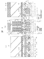
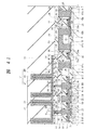
図4は、本実施の形態のDRAM領域のメモリセルの部分(A領域)と周辺回路の一部(B領域)について示した断面図であり、図3におけるC−C線断面を示す。図5は、DRAM領域のメモリセルの部分について示した断面図であり、(a)は図3におけるA−A線断面を、(b)は図3におけるD−D線断面を、(c)は図3におけるB−B線断面を示す。なお、本実施の形態では0.18μmの設計ルールでの製造技術を例示する。
【0053】
半導体基板1の主面には、A領域のp形ウェル2、B領域のp形ウェル3およびn形ウェル4が形成されている。半導体基板1は、たとえば10Ω・cmの抵抗率のp形の単結晶シリコンからなる。また、p形ウェル2の主面にはしきい値電圧調整層5が形成され、p形ウェル2を囲むようにn形のディープウェル6が形成されている。なお、他の各ウェルにも、しきい値電圧調整層が形成されていてもよい。
【0054】
各ウェルの主面には、分離領域7が形成されている。分離領域7はシリコン酸化膜からなり、半導体基板1の主面に形成された浅溝8に埋め込んで形成される。浅溝8は、たとえば0.3μmの深さを有し、内壁には熱酸化されたシリコン酸化膜が形成されてもよい。
【0055】
p形ウェル2の主面にはDRAMのメモリセル選択用MISFETQsが形成されている。また、p形ウェル3およびn形ウェル4の主面には各々nチャネルMISFETQnおよびpチャネルMISFETQpが形成されている。
【0056】
メモリセル選択用MISFETQsは、p形ウェル2の主面上にゲート絶縁膜10を介して形成されたゲート電極11と、ゲート電極11の両側のp形ウェル2の主面に形成された半導体領域12とを有する。
【0057】
ゲート絶縁膜10は、たとえば7〜8nmの膜厚を有する熱酸化により形成されたシリコン酸化膜からなる。
【0058】
ゲート電極11は、たとえば50nmの膜厚の多結晶シリコン膜と100nmの膜厚のタングステンシリサイド(WSi2 )膜との積層膜とすることができる。多結晶シリコン膜には、たとえばリン(P)を3×10²⁰atoms/cm3 程度導入することができる。なお、タングステンシリサイド膜に限られず、コバルトシリサイド(CoSi)膜、チタンシリサイド(TiSi)膜等の他のシリサイド膜であってもよい。また、ゲート電極11は、たとえば膜厚70nmの多結晶シリコン膜、膜厚50nmの窒化チタン膜および膜厚100nmのタングステン膜の積層膜とすることもできる。
【0059】
半導体領域12にはn形の不純物、たとえば砒素(As)またはリンが導入されている。
【0060】
メモリセル選択用MISFETQsのゲート電極11の上層にはシリコン窒化膜からなるキャップ絶縁膜13が形成され、さらにその上層をシリコン窒化膜14で覆われる。キャップ絶縁膜13の膜厚はたとえば200nmであり、シリコン窒化膜14の膜厚はたとえば30nmである。シリコン窒化膜14は、ゲート電極11の側壁にも形成され、後に説明する接続孔を形成する際の自己整合加工に利用される。なお、メモリセル選択用MISFETQsのゲート電極11は、DRAMのワード線として機能するものであり、分離領域7の上面にはワード線WLの一部が形成されている。
【0061】
一方、nチャネルMISFETQnおよびpチャネルMISFETQpは、各々p形ウェル3およびn形ウェル4の主面上に形成され、ゲート絶縁膜10を介して形成されたゲート電極11と、ゲート電極11の両側の各ウェルの主面に形成された半導体領域15とから構成される。ゲート絶縁膜10およびゲート電極11は前記と同様である。半導体領域15は低濃度不純物領域15aと高濃度不純物領域15bとからなり、いわゆるLDD(Lightly Doped Drain )構造を形成している。半導体領域15に導入される不純物は、MISFETの導電形に応じてn形またはp形の不純物が導入される。
【0062】
nチャネルMISFETQnおよびpチャネルMISFETQpのゲート電極11の上層にはシリコン窒化膜からなるキャップ絶縁膜13が形成され、さらにその上層およびゲート電極11とキャップ絶縁膜13との側壁がシリコン窒化膜14で覆われる。キャップ絶縁膜13とシリコン窒化膜14は前記と同様である。
【0063】
メモリセル選択用MISFETQs、nチャネルMISFETQnおよびpチャネルMISFETQpのゲート電極11間のギャップには、絶縁膜16が埋め込まれている。絶縁膜16は、たとえばSOG(Spin On Glass )膜、TEOS(テトラメトキシシラン)を原料ガスとしプラズマCVD法により形成されたシリコン酸化膜(以下TEOS酸化膜という)がCMP(Chemical Mechanical Polishing )法により平坦化されたTEOS酸化膜およびTEOS酸化膜の積層膜とすることができる。
【0064】
絶縁膜16上には配線形成用の絶縁膜17が形成されている。絶縁膜17は、たとえばTEOS酸化膜とすることができる。
【0065】
絶縁膜17には、配線溝18が形成され、配線溝18の側壁にはサイドウォールスペーサ19が形成されている。配線溝18は後に説明するようにフォトリソグラフィによる加工限界で形成される。また、サイドウォールスペーサ19は、たとえばシリコン窒化膜で構成される。サイドウォールスペーサ19はシリコン酸化膜で構成されてもよい。
【0066】
サイドウォールスペーサ19で挟まれた配線溝18の内部には、ビット線BLおよび第1層配線20が形成される。ビット線BLおよび第1層配線20は後に説明するようにCMP法を用いて同時に形成される。ビット線BLおよび第1層配線20は、たとえばタングステン膜から構成されるが、他の金属、たとえば銅膜等を用いてもよい。
【0067】
このように、配線溝18内に埋め込んでビット線BLが形成されるため、後に説明する情報蓄積用容量素子Cまでの層間高さを小さくすることができる。すなわち、ビット線BLを金属膜のフォトリソグラフィによるパターニングを用いて形成しようとすれば、後に説明する接続プラグとビット線BLとを絶縁する絶縁膜が必要であるが、本実施の形態の場合にはそれが必要でない。このため、その絶縁膜の膜厚に相当するだけの層間幅を小さくして素子高さを低減できる。
【0068】
また、配線溝18の内壁にサイドウォールスペーサ19が形成されるため、ビット線BLの幅を小さくすることができる。すなわち、サイドウォールスペーサ19の幅に相当するだけ配線溝18の幅を狭くして、そこに形成されるビット線BLの線幅を細くできる。これは、ビット線BLの線幅をフォトリソグラフィによる加工限界以下の加工精度で形成できることを意味する。このため、後に説明する情報蓄積用容量素子Cと接続プラグとを接続する容量電極接続孔の加工の際に加工マージンを大きくして、容量電極接続孔の加工パターンの合わせずれが発生しても、情報蓄積用容量素子Cとビット線BLとの短絡に起因する不良を発生しない。この結果DRAMの信頼性および製品の歩留まりを向上できる。
【0069】
また、容量電極接続孔の加工マージンを大きくとれるため、従来採用していたような容量電極接続孔の加工の際のビット線BLに対する自己整合加工を採用する必要がない。このため、自己整合加工に必要なビット線BLのキャップ絶縁膜が不要であり、このためキャップ絶縁膜の膜厚に相当するだけ素子の高さを低減できる。この結果、先の素子高さの低減効果とも併せてメモリセル領域(A領域)と周辺回路領域(B領域)との段差を低減し、あるいはB領域の絶縁膜厚さを低減し、段差に起因する第2層以上の配線の加工性の向上とその断線の防止を図ることができ、あるいは第2層配線とその下層の配線等への接続孔の加工性を向上できる。
【0070】
また、ビット線BLの線幅が細く形成できることから、ビット線BL間の距離を大きくしてビット線BL間の線間容量を低減できる。この結果、センスアンプの検出感度を向上してノイズ耐性を向上し、DRAMの性能を向上できる。
【0071】
なお、ビット線BLは配線溝18が形成された絶縁膜17の表面の標高よりも低く形成されている。これは、サイドウォールスペーサ19の上部付近における膜厚が図示するとおり薄くなる傾向にあり、このような場合、サイドウォールスペーサ19の上部付近にまでビット線BLを形成したのではビット線BLの線幅縮小の効果が十分に得られない恐れがある。そのため、後に説明するようにビット線BLおよび第1層配線20の形成の際にCMP法による研磨を過剰に行い、故意にディッシングを発生させてビット線BLの線幅を十分に細く形成したものである。これによりビット線BLの線幅縮小の効果を確実に奏することができる。
【0072】
ビット線BLは接続プラグ21を介して一対のメモリセル選択用MISFETQsに共有される半導体領域12に接続される。接続プラグ21は図3の平面図にも示されるように、活性領域L1のパターンとビット線BLのパターンに重なるようにY方向に長く形成される。なお、ビット線BLと接続プラグ21とは配線溝18の底部で接続されている。これは、後に説明するように配線溝18の形成の際に接続プラグ21の上部が同時に露出されることに基ずく。
【0073】
また、メモリセル選択用MISFETQsの他方の半導体領域12上には情報蓄積用容量素子に接続される接続プラグ22が形成されている。接続プラグ21、22は、n形の不純物たとえばリンが2×10²⁰atoms/cm3 程度導入された多結晶シリコン膜とすることができる。
【0074】
なお、周辺回路領域(B領域)に形成されたnチャネルMISFETQnおよびpチャネルMISFETQpの高濃度不純物領域15bにはビット線BLが直接接続される。このようにビット線BLを高濃度不純物領域15bに直接接続することにより接続プラグを形成した場合に比較して接続プラグの抵抗および接続抵抗を低減し、nチャネルMISFETQnおよびpチャネルMISFETQpの動作速度を向上できる。なお、高濃度不純物領域15bの表面にはコバルト、チタン、タンタル、タングステン等のシリサイド膜を形成できる。
【0075】
ビット線BLおよび第1層配線20は、層間絶縁膜23で覆われている。層間絶縁膜23は、たとえばTEOS酸化膜とすることができる。
【0076】
層間絶縁膜23の上層のA領域には、シリコン窒化膜からなる絶縁膜24が形成され、さらに情報蓄積用の情報蓄積用容量素子Cが形成されている。絶縁膜24は後に説明するように情報蓄積用容量素子Cの下部電極27を形成する際のエッチングストッパとして機能する薄膜である。
【0077】
情報蓄積用容量素子Cは、接続プラグ22に接続プラグ25を介して接続される下部電極27と、たとえばシリコン窒化膜および酸化タンタルからなる容量絶縁膜28と、たとえば窒化チタンからなるプレート電極29とから構成される。接続プラグ25は容量電極接続孔26内に形成され、容量電極接続孔26は前記したとおりビット線BLから十分に離れて形成されるため、ビット線BLと接続プラグ25とが短絡する恐れはない。
【0078】
情報蓄積用容量素子Cの上層には、たとえばTEOS酸化膜からなる絶縁膜30が形成されている。なお、B領域の層間絶縁膜23の上層には情報蓄積用容量素子Cと同層に絶縁膜が形成されてもよい。この絶縁膜により、情報蓄積用容量素子Cの標高に起因するA領域とB領域との間の段差の発生を防止することができ、フォトリソグラフィの焦点深度に余裕を持たせることができ、工程を安定にして微細加工に対応することができる。
【0079】
絶縁膜30の上層には第2層配線31が形成され、第2層配線31と上部電極29あるいは第1層配線20との間はプラグ32で接続される。第2層配線31は、たとえば窒化チタン膜、アルミニウム膜および窒化チタン膜の積層膜とすることができ、プラグ32は、たとえばチタン膜、窒化チタン膜およびタングステン膜の積層膜とすることができる。
【0080】
なお、第2層配線31上にはさらに層間絶縁膜を介して第3層配線あるいはそれ以上の配線層を有してもよいが、説明を省略する。
【0081】
本実施の形態1のDRAMによれば、前記したとおり、ビット線BLを配線溝18内に埋め込んで形成し、また配線溝18の側壁にサイドウォールスペーサ19を形成するため、ビット線BLの線幅を細くできる。これにより容量電極接続孔26の加工を十分な加工マージンをもって行うことができ、接続プラグ25とビット線BLとの短絡を防止できる。また、情報蓄積用容量素子Cの形成される高さを低減することが可能となる。さらに、ビット線BL間の線間容量を低減してDRAMの性能を向上できる。
【0082】
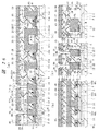
次に、本実施の形態1のDRAMの製造方法を図面を用いて説明する。図6〜図42は本実施の形態1のDRAMの製造方法の一例を工程順に示した断面図または平面図である。なお、特に示さない限り断面図は図3におけるC−C線断面および周辺回路部分の断面を示す。
【0083】
まず、たとえば10Ω・cm程度の抵抗率を有するp形の半導体基板1を用意し、この半導体基板1の主面に深さがたとえば0.3μmの浅溝8を形成する。その後半導体基板1に熱酸化を施し、シリコン酸化膜を形成してもよい。さらにシリコン酸化膜を堆積してこれをCMP法により研磨して浅溝8内にのみシリコン酸化膜を残し、分離領域7を形成する。
【0084】
なお、このときの分離領域7で囲まれる活性領域L1のパターンは、図6(a)に示されるように、直線状の平面パターンである。このため、フォトリソグラフィによる浅溝8の加工において、露光光の干渉等の加工精度の低下要因を極力排除して、フォトリソグラフィの加工限界付近でも精度よく加工を行うことができる。
【0085】
次に、フォトレジストをマスクにして加速エネルギ2300keV、ドーズ量1×10¹³/cm2 のリンイオンを注入してディープウェル6を形成する。次に、フォトレジストをマスクにして加速エネルギ1000keVのリンイオンをドーズ量1×10¹³/cm2 、加速エネルギ460keVのリンイオンをドーズ量3×10¹²/cm2 、加速エネルギ180keVのリンイオンをドーズ量5×10¹¹/cm2 の条件で重ねてイオン注入し、n形ウェル4を形成する。さらにフォトレジストをマスクにして加速エネルギ500keVのボロンイオンをドーズ量1×10¹³/cm2 、加速エネルギ150keVのボロンイオンをドーズ量3×10¹²/cm2 、加速エネルギ50keVのボロンイオンをドーズ量5×10¹¹/cm2 の条件で重ねてイオン注入し、p形ウェル2,3を形成する(図6(b))。さらに半導体基板1の全面に、加速エネルギ70keVの2沸化ボロン(BF2 )イオンをドーズ量1.5×10¹²/cm2 の条件でイオン注入してもよい。
【0086】
次に、p形ウェル2,3、n形ウェル4が形成された活性領域に熱酸化法によりゲート絶縁膜10を形成し、さらに、DRAMのメモリセル領域(A領域)が開口したフォトレジストをマスクとして、加速エネルギ20keVのボロンイオンをドーズ量3×10¹²/cm2 の条件でイオン注入し、メモリセル選択用MISFETQsのしきい値電圧調整層5を形成する(図7)。しきい値電圧調整層5によりメモリセル選択用MISFETQsのしきい電圧を0.7V程度に調整できる。
【0087】
次に、半導体基板1の全面に、たとえば不純物としてリンが3×10²⁰/cm3 の濃度で導入された多結晶シリコン膜を50nmの膜厚で形成し、次に、たとえば100nmの膜厚でタングステンシリサイド膜を堆積する。さらにシリコン窒化膜をたとえば200nmの膜厚で堆積する。多結晶シリコン膜およびシリコン窒化膜は、たとえばCVD(Chemical Vapor Deposition )法により、タングステンシリサイド膜はスパッタ法により形成できる。その後、シリコン窒化膜、タングステンシリサイド膜および多結晶シリコン膜をフォトリソグラフィ技術およびエッチング技術を用いてパターニングし、ゲート電極11(ワード線WL)およびキャップ絶縁膜13を形成する(図8(b))。このときのワード線WL(キャップ絶縁膜13も同様である。)のパターンを図8(a)に示す。ワード線WLは、直線状にパターニングされており、フォトリソグラフィがその加工限界においても容易に行うことができることがわかる。
【0088】
次に、キャップ絶縁膜13およびゲート電極11とフォトレジストをマスクとして、メモリセルが形成される領域(A領域)および周辺回路領域(B領域)のnチャネルMISFETQnが形成される領域に不純物たとえばヒ素(As)またはリンをイオン注入し、半導体領域12およびnチャネルMISFETQnの低濃度不純物領域15aを形成する。その後、周辺回路領域(B領域)のpチャネルMISFETQpが形成される領域に不純物たとえばボロン(B)をイオン注入し、pチャネルMISFETQpの低濃度不純物領域15aを形成する(図9)。
【0089】
次に、半導体基板1の全面にシリコン窒化膜14を、たとえば30nmの膜厚で堆積する。なお、メモリセルが形成される領域(A領域)にのみ形成されたフォトレジスト膜をマスクとして、シリコン窒化膜14を異方性エッチングし、A領域の半導体基板1上にのみシリコン窒化膜14を残存させると同時にB領域のゲート電極11の側壁にサイドウォールスペーサを形成してもよい。
【0090】
次に、メモリセルが形成される領域(A領域)および周辺回路領域(B領域)のnチャネルMISFETQnが形成される領域にフォトレジスト膜を形成し、このフォトレジスト膜とシリコン窒化膜14をマスクにして不純物たとえばボロンをイオン注入し、pチャネルMISFETQpの高濃度不純物領域15bを形成し、さらに、メモリセルが形成される領域(A領域)および周辺回路領域(B領域)のpチャネルMISFETQpが形成される領域にフォトレジスト膜を形成し、このフォトレジスト膜とシリコン窒化膜14をマスクにして不純物たとえばリンをイオン注入し、nチャネルMISFETQnの高濃度不純物領域15bを形成しおよびを形成する(図10)。
【0091】
次に、たとえば膜厚が400nmのシリコン酸化膜をCVD法により形成し、さらにこのシリコン酸化膜をCMP(Chemical Mechanical Polishing )法により研磨して平坦化し、絶縁膜16を形成する。
【0092】
この後、図11に示すような接続プラグ21および接続プラグ22のパターンに相当する接続孔を開口し、プラグインプラを施した後に不純物がドープされた多結晶シリコン膜を堆積し、この多結晶シリコン膜をCMP法により研磨して接続プラグ21、22を形成する(図12)。なお、図12において、(a)は図3におけるC−C線断面および周辺回路部分の断面を示し、(b)は図3におけるA−A線断面を、(c)は図3におけるD−D線断面を、(d)は図3におけるB−B線断面を示す。以下、図13、14、16、17、19、20、22、23、25〜27において同様である。
【0093】
プラグインプラは、たとえばリンイオンを加速エネルギ50keV、ドーズ量1×10¹³/cm2 とすることができる。また、多結晶シリコン膜への不純物の導入は、たとえばCVD法により濃度2×10²⁰/cm3 のリンを導入して行うことができる。なお、この接続孔は、2段階のエッチングにより開口して半導体基板1の過剰エッチングを防止することができる。また、接続プラグ21、22の形成はエッチバック法により形成することもできる。
【0094】
次に、配線形成用の絶縁膜17を形成する(図13)。絶縁膜17は、たとえばCVD法によるシリコン酸化膜とすることができ、膜厚は、たとえば200nmとする。
【0095】
次に、絶縁膜17に深さが200nmの配線溝18を形成する(図14)。配線溝18は、フォトリソグラフィの加工限界で形成され、たとえば0.18μmの溝幅で形成される。図15にその平面パターンを示す。配線溝18は直線形状のパターンで形成されるため、フォトリソグラフィの加工限界においても十分な加工精度で形成できる。
【0096】
次に、配線溝18を覆う絶縁膜33を半導体基板1の全面に堆積する(図16)。絶縁膜33は、たとえばCVD法により形成されたシリコン酸化膜あるいはシリコン窒化膜とすることができ、その膜厚は、たとえば60nmとする。
【0097】
次に、絶縁膜33を異方性エッチングすることにより、配線溝18の側壁にサイドウォールスペーサ19を形成する(図17)。サイドウォールスペーサ19の厚さは、絶縁膜33の厚さで規定され、ほぼ60nmである。このように、サイドウォールスペーサ19を形成するため、配線溝18の溝幅をサイドウォールスペーサ19の厚さに相当するだけ狭くすることができる。すなわち、フォトリソグラフィの加工限界である0.18μmで加工される配線溝18の幅を、厚さ60nmのサイドウォールスペーサ19に挟まれた幅である60nmまで狭くすることができる。これは、後に説明するビット線BLの幅をフォトリソグラフィの加工限界である0.18μmよりも細い60nmで形成できることを意味する。
【0098】
なお、この異方性エッチング工程により、絶縁膜16の一部が過剰にエッチングされ、配線溝18が若干深く形成されるが、これにより接続プラグ21の表面を確実に露出することができる(図17(b))。これにより接続プラグ21とビット線BLとの接続を信頼性よく行える。また、配線溝18の加工およびサイドウォールスペーサ19の加工により、接続プラグ21との接続部の露出が同時に行える。従来法では、ビット線と接続プラグとを接続する接続孔を加工した後にビット線の形成を行っていたが、本実施の形態の方法では、このような接続孔の加工工程が不要である。このため工程を簡略化できる。さらに、サイドウォールスペーサ19の加工の際の過剰エッチングにより、配線溝18が若干深く形成されるため、ビット線BLの高さを高くしてその断面積を大きくすることができる。このビット線BLの断面積を増加する効果は、後に説明するように、ビット線BLと周辺回路の第1層配線20とが同時に形成されるため、第1層配線20の抵抗値の低減効果としても同時に得られる。このためビット線BLおよび第1層配線20の抵抗値を低減してDRAMの性能を向上できる。
【0099】
次に、周辺回路領域(B領域)の高濃度不純物領域15b上に開口を有するフォトレジスト膜をマスクとして、接続孔34を形成する(図18)。接続孔34は、後に説明する第1層配線20を直接高濃度不純物領域15bに接続するためのものであり、これにより周辺回路領域(B領域)での配線抵抗を低減してDRAMの性能を向上できる。なお、接続孔34が形成される領域にはあらかじめ接続プラグを形成していてもよい。
【0100】
次に、たとえばスパッタ法により、膜厚が300nmのタングステン膜35を半導体基板1の全面に形成する(図19)。ここでは、タングステン膜35を例示しているが、他の金属膜、たとえば、銅膜等を用いてもよい。ただし、半導体基板1への金属原子の熱拡散による信頼性の低下を考慮すれば、金属膜は高融点金属であることが好ましい。たとえばモリブデン、タンタル、ニオブ等を例示できる。
【0101】
次に、タングステン膜35を、たとえばCMP法により研磨し、配線溝18およびサイドウォールスペーサ19の上部以外のタングステン膜35を除去し、ビット線BLおよび第1層配線20を形成する(図20)。このときのビット線BLの平面パターンを図21に示す。ビット線BLはサイドウォールスペーサ19に挟まれた配線溝18に形成され、その配線幅は約60nmである。
【0102】
なお、第1層配線20と高濃度不純物領域15bとの接続部は、前記タングステン膜35の形成工程において接続孔34の内部にもタングステン膜35が埋め込まれるため、本工程で同時に形成される。
【0103】
また、このタングステン膜35の研磨工程において、CMP法による研磨を過剰に行い、タングステン膜35の表面を配線溝18が形成される絶縁膜17の表面よりも、つまりサイドウォールスペーサ19の上端部よりも低く形成できる。このように、タングステン膜35の表面を低く形成するため、ビット線BLの線幅縮小の効果を有効に奏することができる。すなわち、サイドウォールスペーサ19の上端部は図20(c)等に示すように一般に薄くなる。このような場合に、サイドウォールスペーサ19の上端部にまでビット線BLを形成すると、ビット線BLの下部の線幅が十分に細くなっているにもかかわらず、ビット線BLの上部の線幅が太くなり、その線幅縮小の効果を十分に発揮できない。そこで、本実施の形態では、CMP法による研磨を過剰に行い、ビット線BLおよび第1層配線20の形成される領域に積極的にディッシングを発生させて、その表面をサイドウォールスペーサ19の上端部よりも低く形成させている。なお、CMP法による研磨条件を調整し、配線溝18が形成される絶縁膜17およびサイドウォールスペーサ19をタングステン膜35と同時に研磨して除去してもよい。
【0104】
なお、タングステン膜35の除去にはエッチバック法を用いることもできる。
【0105】
次に、半導体基板1の全面に、たとえばCVD法によりシリコン酸化膜を堆積し、このシリコン酸化膜をCMP法により研磨して平坦化し、層間絶縁膜23を形成する(図22)。
【0106】
次に、半導体基板1の全面にシリコン窒化膜24および多結晶シリコン膜36を堆積する(図23)。多結晶シリコン膜36には、たとえば3×10²⁰/cm3 の濃度のリンを導入でき、その膜厚はたとえば100nmである。
【0107】
次に、図24に示すようなSNCTのパターンで、多結晶シリコン膜36に開口37を形成する。開口37の口径はたとえば0.22μmである。その後、半導体基板1の全面に多結晶シリコン膜36と同様の多結晶シリコン膜を膜厚70nmで堆積し、これを異方性エッチングして開口37の側壁にサイドウォールスペーサ38を形成する(図25)。サイドウォールスペーサ38の幅は約70nmとなり、開口37の口径はサイドウォールスペーサ38により80nmに縮小される。
【0108】
次に、多結晶シリコン膜36およびサイドウォールスペーサ38をハードマスクとしてエッチングを行い、容量電極接続孔26を形成する(図26)。容量電極接続孔26の口径は80nmであり、その深さは約300nmである。
【0109】
このように容量電極接続孔26の口径を小さく形成できるため、開口37を形成するためのマスクに合わせずれが発生しても、ビット線BLと接触することがない。また、ビット線BLの線幅が十分にひらいているため、その効果がより確実に発揮される。
【0110】
次に、容量電極接続孔26を埋め込む多結晶シリコン膜を堆積し、この多結晶シリコン膜、多結晶シリコン膜36およびサイドウォールスペーサ38をCMP法またはエッチバック法により除去して容量電極接続孔26の内部に接続プラグ25を形成する(図27)。前記したとおり、接続プラグ25とビット線BLとが短絡されることはない。接続プラグ25には、たとえば3×10²⁰/cm3 の濃度のリンを導入できる。なお、多結晶シリコン膜、多結晶シリコン膜36およびサイドウォールスペーサ38の際には、シリコン窒化膜24をCMP法またはエッチバック法のエッチストッパ膜として機能させることができる。
【0111】
次に、たとえばCVD法によりシリコン酸化膜からなる絶縁膜39を堆積し、情報蓄積用容量素子Cが形成される領域に溝40を形成する(図28、図29、図30)。なお、図29において(a)は図3におけるA−A線断面を、(b)は図3におけるD−D線断面を、(c)は図3におけるB−B線断面を示す。以下、図32、34、36、38、40、42において同様である。
【0112】
絶縁膜39の堆積はプラズマCVDにより行うことができ、その膜厚はたとえば1.2μmとする。
【0113】
次に、溝40を覆う多結晶シリコン膜41を半導体基板1の全面に堆積し(図31、32)、さらに半導体基板1の全面にシリコン酸化膜42を堆積する(図33、34)。多結晶シリコン膜41にはリンをドープすることができ、その膜厚は0.03μmとすることができる。多結晶シリコン膜41の膜厚が溝40の寸法に対して十分に薄いため、多結晶シリコン膜41は溝40の内部にもステップカバレッジよく堆積される。シリコン酸化膜42は、溝40の内部に埋め込まれるように堆積する。溝40の内部への埋め込み性を考慮すれば、シリコン酸化膜42はSOG膜あるいはTEOSを用いたCVD法によるシリコン酸化膜とすることができる。
【0114】
次に、絶縁膜39上のシリコン酸化膜42および多結晶シリコン膜41を除去して、情報蓄積用容量素子Cの下部電極27を形成する(図35、36)。シリコン酸化膜42および多結晶シリコン膜41の除去はエッチバック法またはCMP法により行うことができる。また、下部電極27の内部には、シリコン酸化膜42が残存している。
【0115】
次に、ウェットエッチングを施し、絶縁膜39およびシリコン酸化膜42を除去する(図37、38)。これにより下部電極27が露出される。なお、周辺回路領域(B領域)にフォトレジスト膜を形成し、これをマスクとしてB領域に絶縁膜39を残存させてもよい。
【0116】
なお、シリコン窒化膜24はウェットエッチング工程でのエッチングストッパとして機能する。
【0117】
次に、下部電極27表面を窒化または酸窒化処理した後、酸化タンタル膜を堆積し容量絶縁膜28を形成する。酸化タンタル膜の堆積は、有機タンタルガスを原料としたCVD法により形成できる。この段階での酸化タンタル膜はアモルファス構造を有するものである。ここで酸化タンタル膜に熱処理を施して結晶化(多結晶化)された酸化タンタル膜(Ta2 O5 )とし、より強固な誘電体として容量絶縁膜28を形成してもよい。また、容量絶縁膜28はシリコン酸化膜に換算して5nmの膜厚のシリコン窒化膜としてもよい。さらに、たとえば窒化チタン膜43をCVD法により堆積する(図39、40)。
【0118】
その後、フォトレジスト膜を用いて窒化チタン膜および多結晶酸化タンタル膜をパターニングし、容量絶縁膜28およびプレート電極29を形成する。このようにして下部電極27、容量絶縁膜28およびプレート電極29からなる情報蓄積用容量素子Cが形成される。さらに半導体基板1の全面に絶縁膜30を形成する(図41、42)。なお、プレート電極29は、窒化チタン膜に代えて、たとえば4×10²⁰/cm3 の濃度のリンを含む多結晶シリコン膜としてもよい。
【0119】
次に、絶縁膜30に接続孔を形成し、その接続孔を含む絶縁膜30上に、たとえばチタン膜、窒化チタン膜およびタングステン膜を順次堆積し、これをCMP法またはエッチバック法により除去してプラグ32を形成し、この後、絶縁膜30上にたとえば窒化チタン膜、アルミニウム膜および窒化チタン膜からなる積層膜を堆積し、これをパターニングして第2層配線31を形成する。これにより図4および図5に示すDRAMをほぼ完成する。さらに上層の配線層は第2層配線31と同様に形成できるため、その詳細な説明は省略する。
【0120】
本実施の形態のDRAMによれば、ビット線BLの線幅が80nm、容量電極接続孔26の直径が80nmに形成することができ、両者の合わせ余裕を0.15μmと0.2μm製造技術では十分に大きな余裕を確保することができる。これによって、セル面積が0.4×0.8=0.32μm2 という微細なDRAMセルを加工上の問題なく製造することが可能である。また、接続プラグ21、22の上面から情報蓄積用容量素子Cの下部電極27の下面までの距離はわずかに0.3μmに抑えることができ、結果的に基板表面からプレート電極29の上面までのセルの高さを低くできる。
【0121】
なお、本実施の形態1では、図17に示す工程において、サイドウォールスペーサ19の加工の際のエッチングを過剰に行い、配線溝18の底部を深く形成する場合を説明したが、図43に示すように、過剰なエッチングを行わず、配線溝18の深さを絶縁膜17の膜厚程度に止めることができる。この場合であっても、図44に示すように、接続プラグ21の表面が配線溝18の底部で露出する限り、ビット線BLと接続プラグ21との接続が行われ、DRAMを正常に機能させることができる。
【0122】
また、配線溝18が形成される絶縁膜17の底部にシリコン窒化膜を形成することも可能である。すなわち、図45に示すように、絶縁膜16を形成した後、シリコン窒化膜44を形成し、シリコン窒化膜44と絶縁膜17に接続孔を形成してこの接続孔に接続プラグ21、22を形成する。この後、前記図13〜17の工程と同様に絶縁膜17に配線溝18を形成し(図46)、さらにサイドウォールスペーサ19を形成する(図47)。この場合、シリコン窒化膜44がが形成されているため、配線溝18の加工の際のエッチング、あるいはサイドウォールスペーサ19の加工の際のエッチングにおいてシリコン窒化膜44をエッチングストッパとして機能させることができる。
【0123】
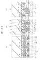
(実施の形態2)
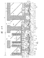
図48は、実施の形態2のDRAMのメモリアレイMARYの一部を拡大した平面図である。また、図49は、本実施の形態のDRAM領域のメモリセルの部分(A領域)と周辺回路の一部(B領域)について示した断面図であり、図48におけるC−C線断面を示す。図50は、DRAM領域のメモリセルの部分について示した断面図であり、(a)は図48におけるA−A線断面を、(b)は図48におけるD−D線断面を、(c)は図48におけるB−B線断面を示す。
【0124】
本実施の形態2のDRAMは、実施の形態1におけるDRAMと、そのビット線BLと半導体領域12との接続部分において相違するのみであり、他の構成についてはほぼ同様である。したがって、その相違する部分についてのみ以下に説明し、同様の構成部分については説明を省略する。
【0125】
本実施の形態2のDRAMでは、活性領域L1の中央部分の半導体領域12とビット線BLとが実施の形態1の接続プラグ21を介して接続されず、ビット線BLと一体に形成される接続部BLCにおいて直接半導体領域12と接続される。したがって、ビット線BLの平面パターンと活性領域L1の平面パターンとは、その平行位置にずれが存在するため、互いに重複した領域を確保するために図48に示すように、活性領域L1においてはビット線BLの方向に突き出した張り出し領域L11を有し、ビット線BLのにおいては接続部BLCが活性領域L1の方向に張り出して形成される。
【0126】
次に、本実施の形態2のDRAMの製造方法を説明する。図51〜図60は、本実施の形態2のDRAMの製造方法の一例を工程順に示した断面図または平面図である。なお、断面図において、(a)は図48におけるC−C線断面および周辺回路部分の断面を示し、(b)は図48におけるA−A線断面を、(c)は図48におけるD−D線断面を、(d)は図48におけるB−B線断面を示す。
【0127】
まず実施の形態1と同様に分離領域7を形成する。この分離領域7は、図51に示されるような活性領域L1のパターンで形成され、張り出し領域L11を有する。
【0128】
次に、実施の形態1における図10までの工程と同様に各部材を形成し、実施の形態1と同様に絶縁膜16を形成する(図52)。
【0129】
次に、図53に示すようなSNCTのパターンで接続孔を形成し、接続プラグ22を実施の形態1と同様に形成する(図54)。
【0130】
次に、実施の形態1における図13の工程と同様に、配線形成用の絶縁膜17を形成し、さらに実施の形態1における図14と同様に、絶縁膜17に配線溝18を形成する。この配線溝18を形成した状態の平面図を図55に示す。
【0131】
次に、図56に示す接続孔BLCTのパターンで、配線溝18に重ねて接続孔BLCTを形成する(図57)。接続孔BLCTの形成は、接続プラグ22が形成される接続孔の形成と同様に行うことができる。
【0132】
次に、実施の形態1の図16の工程と同様に、絶縁膜33を形成し、この絶縁膜33を異方性エッチングすることにより配線溝18の側壁にサイドウォールスペーサ19を形成する(図58)。このとき、絶縁膜33は、接続孔BLCTの内部にまで形成されるため、サイドウォールスペーサ19は接続孔BLCTの内壁にも形成される。
【0133】
次に、実施の形態1における図19および図20の工程と同様に、サイドウォールスペーサ19でその幅が狭められた配線溝18の内部にビット線BLおよび第1層配線20を形成する(図59)。なお、接続孔BLCTの内部には、ビット線BLと一体に形成された接続部BLCが形成される。この状態の平面図を図60に示す。
【0134】
この後の工程は実施の形態1と同様であるため説明を省略する。
【0135】
本実施の形態のDRAMによれば、ビット線BLと半導体基板1の半導体領域12に接続される接続部BLCとが一体で形成されるため、工程を簡略化し、また、その部分での接続抵抗を低減してDRAMの性能を向上できる。また、実施の形態1と同様に、ビット線BLの配線幅の縮小の効果、セル高さの低減の効果、およびビット線線間容量の低減効果が同様に得られることはいうまでもない。
【0136】
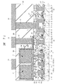
(実施の形態3)
図61は、実施の形態3のDRAMのメモリアレイMARYの一部を拡大した平面図である。また、図62は、本実施の形態のDRAM領域のメモリセルの部分(A領域)と周辺回路の一部(B領域)について示した断面図であり、図61におけるC−C線断面を示す。図63は、DRAM領域のメモリセルの部分について示した断面図であり、(a)は図61におけるA−A線断面を、(b)は図61におけるD−D線断面を、(c)は図16におけるB−B線断面を示す。
【0137】
本実施の形態3のDRAMは、実施の形態1におけるDRAMと、そのビット線BLと半導体領域12との接続部分において相違するのみであり、他の構成についてはほぼ同様である。したがって、その相違する部分についてのみ以下に説明し、同様の構成部分については説明を省略する。
【0138】
本実施の形態3のDRAMでは、活性領域L1の中央部分の半導体領域12とビット線BLとが実施の形態1の接続プラグ21を介して接続されず、前記半導体領域12を平面的に覆うパターンで形成された導電膜45を介して接続される。導電膜45は、絶縁膜46上に形成され、たとえばリン等の不純物が導入された多結晶シリコン膜からなり、接続孔BLCTを介して半導体領域12に接続されている。
【0139】
また、本実施の形態3のDRAMでは、活性領域L1の両端の半導体領域12と情報蓄積用容量素子Cの下部電極27とが、実施の形態1の接続プラグ22および接続プラグ25とを介して接続されず、接続プラグ25のみで接続される。
【0140】
なお、絶縁膜46は、実施の形態1で説明したような2段階エッチングを行う必要がないため、シリコン窒化膜で構成する必要はなく、シリコン酸化膜で構成できる。また、本実施の形態3のDRAMでは、配線溝18を形成するための絶縁膜47が、ゲート電極11を覆う絶縁膜をも兼ねるため、実施の形態1の絶縁膜16、17を別々に形成する必要はなく、後に説明するように工程を短縮できる。
【0141】
次に、本実施の形態3のDRAMの製造方法を説明する。図64〜図69は、本実施の形態3のDRAMの製造方法の一例を工程順に示した断面図または平面図である。なお、断面図において、(a)は図61におけるC−C線断面および周辺回路部分の断面を示し、(b)は図61におけるA−A線断面を、(c)は図61におけるD−D線断面を、(d)は図61におけるB−B線断面を示す。
【0142】
本実施の形態3のDRAMの製造方法は、実施の形態1における図10までの工程と同様である。ただし、絶縁膜46は、たとえばCVD法により形成されたシリコン酸化膜で構成する。この後、図64に示すような接続孔BLCTのパターンで、絶縁膜46に接続孔BLCTを形成する(図65)。このとき、ゲート電極11の側壁には、絶縁膜46のサイドウォールスペーサが形成される。
【0143】
次に、半導体基板1の全面に、たとえば、リンが導入された多結晶シリコン膜を堆積し、この多結晶シリコン膜を図66で示した導電膜45のパターンでパターニングする。これにより絶縁膜46上に導電膜45を形成する(図67)。
【0144】
次に、半導体基板1の全面に、たとえばCVD法により形成されたシリコン酸化膜からなる絶縁膜を堆積し、この絶縁膜をCMP法により研磨して配線形成用の絶縁膜47を形成する。
【0145】
ここまでの工程を実施の形態1の工程と比較すれば、実施の形態1においては、接続プラグ21、22を形成するための絶縁膜16の形成において、および、配線形成用の絶縁膜17の形成において、2回のCMP法による研磨工程を必要とする。これに対し、本実施の形態3では、配線形成用の絶縁膜47を形成するためのCMP法による研磨工程の1回のみであり、実施の形態1と比較して少ないCMP法による研磨工程で済む。CMP法による研磨工程では、半導体基板1の全面においてその平坦性をある程度確保する必要性から、必然的に絶縁膜の膜厚が大きくなり、このため、多くのCMP工程を有する方法により製造された半導体集積回路装置は、一般に標高が高くなる。このように標高が高くなると、上層配線の接続を行うための接続孔の深さが深くなる等の加工上好ましくない状況が発生する。しかし、本実施の形態3では、実施の形態1に比較してCMP工程が少なくなり、工程が簡略化、短縮化されるのみならず、素子の標高の増加を抑制して、上層配線および接続部材の加工を容易にすることが可能となる。
【0146】
次に、実施の形態1と同様に、絶縁膜47に配線溝18を形成し、さらに配線溝18の側壁にサイドウォールスペーサ19を形成する(図68)。なお、図68においては、周辺回路の領域(B領域)に接続孔を形成した段階を示している。
【0147】
次に、実施の形態1における図19および図20の工程と同様に、サイドウォールスペーサ19でその幅が狭められた配線溝18の内部にビット線BLおよび第1層配線20を形成する(図69)。
【0148】
この後の工程は実施の形態1と同様であるため説明を省略する。なお、本実施の形態3のDRAMでは、接続プラグ22が形成されていないため、容量電極接続孔26を半導体基板1の半導体領域12に達するまで加工し、その内部に実施の形態1と同様にたとえば多結晶シリコン膜を形成して接続プラグ25を形成する。
【0149】
本実施の形態のDRAMによれば、ビット線BLと半導体領域12とを導電膜45を介して接続し、絶縁膜47で配線形成用の絶縁膜とゲート電極11を埋め込む絶縁膜とを兼ねることができるため、工程を短縮し、またCMP工程を少なくして素子高さを抑制できる。また、実施の形態1と同様に、ビット線BLの配線幅の縮小の効果、セル高さの低減の効果、およびビット線線間容量の低減効果が同様に得られることはいうまでもない。
【0150】
以上、本発明者によってなされた発明を発明の実施の形態に基づき具体的に説明したが、本発明は前記実施の形態に限定されるものではなく、その要旨を逸脱しない範囲で種々変更可能であることは言うまでもない。
【0151】
たとえば、実施の形態1〜3では、情報蓄積用容量素子Cとして、上方に開口を有する円筒形状の下部電極を有する情報蓄積用容量素子の例を示したが、図70あるいは図71に示すような、情報蓄積用容量素子を用いてもよい。
【0152】
すなわち、図71は、実施の形態1における絶縁膜39の溝40内に形成された多結晶シリコン膜41の内面を用いて下部電極を構成するものであり、絶縁膜39をエッチングにより除去することなく残存させるものである。この場合、シリコン窒化膜24は必要でない。
【0153】
また、図71は、単純スタック構造の下部電極を採用する場合の例であり、実施の形態1の図26の後、容量電極接続孔26を埋め込むと同時に、下部電極を構成する多結晶シリコン膜を同時に形成し、この多結晶シリコン膜と実施の形態1の多結晶シリコン膜36をパターニングして下部電極を形成するものである。なお、サイドウォールスペーサ38は下部電極の一部として構成される。また、シリコン窒化膜24は本構成においても必要でない。
【0154】
また、本実施の形態のビット線BLの形成方法は、DRAMに限られず、DRAMを混載したロジック回路や、DRAMを混載したフラッシュメモリ内臓のマイクロコンピュータ、その他のシステム混載チップへの適用が可能である。
【0155】
【発明の効果】
本願において開示される発明のうち、代表的なものによって得られる効果を簡単に説明すれば以下のとおりである。
【0156】
(1)ビット線等配線の線幅をフォトリソグラフィの加工限界を越えて縮小された寸法で加工できる。
【0157】
(2)メモリセルの高さを大きくすることなく、ビット線と情報蓄積用容量素子の下部電極との短絡を防止することができる。
【0158】
(3)メモリセルの高さを低くできる。
【0159】
(4)ビット線容量を低減し、検出感度が高く、ノイズ耐性に優れた半導体集積回路装置を提供できる。
【0160】
(5)フォトリソグラフィに適した単純な平面パターンを採用した半導体集積回路装置の構造が提供でき、加工マージンを向上できる。
【0161】
(6)DRAMの高集積化に適した半導体集積回路装置の構造および製造方法を提供でき、半導体集積回路装置の信頼性、歩留まりおよび性能を向上できる。
【図面の簡単な説明】
【図1】本発明の一実施の形態であるDRAMを形成した半導体チップ全体の一例を示した平面図である。
【図2】本実施の形態1のDRAMの等価回路図である。
【図3】図1のメモリアレイMARYの一部を拡大した平面図である。
【図4】実施の形態1のDRAM領域のメモリセルの部分と周辺回路の一部について示した断面図であり、図3におけるC−C線断面を示す。
【図5】実施の形態1のDRAM領域のメモリセルの部分について示した断面図であり、(a)は図3におけるA−A線断面を、(b)は図3におけるD−D線断面を、(c)は図3におけるB−B線断面を示す。
【図6】(a)は実施の形態1のDRAMの製造方法の一例を工程順に示した平面図であり、(b)は実施の形態1のDRAMの製造方法の一例を工程順に示した断面図である。
【図7】実施の形態1のDRAMの製造方法の一例を工程順に示した断面図である。
【図8】(a)は実施の形態1のDRAMの製造方法の一例を工程順に示した平面図であり、(b)は実施の形態1のDRAMの製造方法の一例を工程順に示した断面図である。
【図9】実施の形態1のDRAMの製造方法の一例を工程順に示した断面図である。
【図10】実施の形態1のDRAMの製造方法の一例を工程順に示した断面図である。
【図11】実施の形態1のDRAMの製造方法の一例を工程順に示した平面図である。
【図12】実施の形態1のDRAMの製造方法の一例を工程順に示した断面図である。
【図13】実施の形態1のDRAMの製造方法の一例を工程順に示した断面図である。
【図14】実施の形態1のDRAMの製造方法の一例を工程順に示した断面図である。
【図15】実施の形態1のDRAMの製造方法の一例を工程順に示した平面図である。
【図16】実施の形態1のDRAMの製造方法の一例を工程順に示した断面図である。
【図17】実施の形態1のDRAMの製造方法の一例を工程順に示した断面図である。
【図18】実施の形態1のDRAMの製造方法の一例を工程順に示した断面図である。
【図19】実施の形態1のDRAMの製造方法の一例を工程順に示した断面図である。
【図20】実施の形態1のDRAMの製造方法の一例を工程順に示した断面図である。
【図21】実施の形態1のDRAMの製造方法の一例を工程順に示した平面図である。
【図22】実施の形態1のDRAMの製造方法の一例を工程順に示した断面図である。
【図23】実施の形態1のDRAMの製造方法の一例を工程順に示した断面図である。
【図24】実施の形態1のDRAMの製造方法の一例を工程順に示した平面図である。
【図25】実施の形態1のDRAMの製造方法の一例を工程順に示した断面図である。
【図26】実施の形態1のDRAMの製造方法の一例を工程順に示した断面図である。
【図27】実施の形態1のDRAMの製造方法の一例を工程順に示した断面図である。
【図28】実施の形態1のDRAMの製造方法の一例を工程順に示した断面図である。
【図29】実施の形態1のDRAMの製造方法の一例を工程順に示した断面図である。
【図30】実施の形態1のDRAMの製造方法の一例を工程順に示した平面図である。
【図31】実施の形態1のDRAMの製造方法の一例を工程順に示した断面図である。
【図32】実施の形態1のDRAMの製造方法の一例を工程順に示した断面図である。
【図33】実施の形態1のDRAMの製造方法の一例を工程順に示した断面図である。
【図34】実施の形態1のDRAMの製造方法の一例を工程順に示した断面図である。
【図35】実施の形態1のDRAMの製造方法の一例を工程順に示した断面図である。
【図36】実施の形態1のDRAMの製造方法の一例を工程順に示した断面図である。
【図37】実施の形態1のDRAMの製造方法の一例を工程順に示した断面図である。
【図38】実施の形態1のDRAMの製造方法の一例を工程順に示した断面図である。
【図39】実施の形態1のDRAMの製造方法の一例を工程順に示した断面図である。
【図40】実施の形態1のDRAMの製造方法の一例を工程順に示した断面図である。
【図41】実施の形態1のDRAMの製造方法の一例を工程順に示した断面図である。
【図42】実施の形態1のDRAMの製造方法の一例を工程順に示した断面図である。
【図43】実施の形態1のDRAMの製造方法の他の例を工程順に示した断面図である。
【図44】実施の形態1のDRAMの製造方法の他の例を工程順に示した断面図である。
【図45】実施の形態1のDRAMの製造方法のさらに他の例を工程順に示した断面図である。
【図46】実施の形態1のDRAMの製造方法のさらに他の例を工程順に示した断面図である。
【図47】実施の形態1のDRAMの製造方法のさらに他の例を工程順に示した断面図である。
【図48】実施の形態2のDRAMのメモリアレイMARYの一部を拡大した平面図である。
【図49】実施の形態2のDRAM領域のメモリセルの部分と周辺回路の一部について示した断面図であり、図48におけるC−C線断面を示す。
【図50】実施の形態2のDRAM領域のメモリセルの部分について示した断面図であり、(a)は図48におけるA−A線断面を、(b)は図48におけるD−D線断面を、(c)は図48におけるB−B線断面を示す。
【図51】実施の形態2のDRAMの製造方法の一例を工程順に示した平面図である。
【図52】実施の形態2のDRAMの製造方法の一例を工程順に示した断面図である。
【図53】実施の形態2のDRAMの製造方法の一例を工程順に示した平面図である。
【図54】実施の形態2のDRAMの製造方法の一例を工程順に示した断面図である。
【図55】実施の形態2のDRAMの製造方法の一例を工程順に示した平面図である。
【図56】実施の形態2のDRAMの製造方法の一例を工程順に示した平面図である。
【図57】実施の形態2のDRAMの製造方法の一例を工程順に示した断面図である。
【図58】実施の形態2のDRAMの製造方法の一例を工程順に示した断面図である。
【図59】実施の形態2のDRAMの製造方法の一例を工程順に示した断面図である。
【図60】実施の形態2のDRAMの製造方法の一例を工程順に示した平面図である。
【図61】実施の形態3のDRAMのメモリアレイMARYの一部を拡大した平面図である。
【図62】実施の形態3のDRAM領域のメモリセルの部分と周辺回路の一部について示した断面図であり、図61におけるC−C線断面を示す。
【図63】実施の形態3のDRAM領域のメモリセルの部分について示した断面図であり、(a)は図61におけるA−A線断面を、(b)は図61におけるD−D線断面を、(c)は図16におけるB−B線断面を示す。
【図64】実施の形態3のDRAMの製造方法の一例を工程順に示した平面図である。
【図65】実施の形態3のDRAMの製造方法の一例を工程順に示した断面図である。
【図66】実施の形態3のDRAMの製造方法の一例を工程順に示した平面図である。
【図67】実施の形態3のDRAMの製造方法の一例を工程順に示した断面図である。
【図68】実施の形態3のDRAMの製造方法の一例を工程順に示した断面図である。
【図69】実施の形態3のDRAMの製造方法の一例を工程順に示した断面図である。
【図70】本発明のさらに他の実施の形態であるDRAMの一例を示した断面図である。
【図71】本発明のさらに他の実施の形態であるDRAMの他の例を示した断面図である。
【図72】容量電極接続孔の加工上の課題を説明するための断面図であり、ビット線の延在方向に垂直な方向でのメモリセル部の断面を示している。
【符号の説明】
1 半導体基板
1A 半導体チップ
2、3 p形ウェル
4 n形ウェル
5 ドーズ量
6 ディープウェル
7 分離領域
8 浅溝
10 ゲート絶縁膜
11 ゲート電極
12、15 半導体領域
13 キャップ絶縁膜
14 シリコン窒化膜
15a 低濃度不純物領域
15b 高濃度不純物領域
16、17、30、33、3946、47 絶縁膜
18 配線溝
19、38 サイドウォールスペーサ
20 第1層配線
21、22、25 接続プラグ
23 層間絶縁膜
24 絶縁膜(シリコン窒化膜)
26 容量電極接続孔
27 下部電極
28 容量絶縁膜
29 プレート電極
29 上部電極
31 第2層配線
32 プラグ
34 接続孔
35 タングステン膜
36、41 多結晶シリコン膜
37 開口
40 溝
42 シリコン酸化膜
43 窒化チタン膜
44 シリコン窒化膜
45 導電膜
201 半導体基板
202 分離領域
203 活性領域
204 半導体領域
205 接続プラグ
206 上部電極
207 容量絶縁膜
208 下部電極
209 ビット線
210 容量電極接続孔
211 合わせ余裕
212 シリコン窒化膜
213 サイドウォールスペーサ
214、215 シリコン酸化膜
BL ビット線
BLC 接続部
BLCT 接続孔
BP 接続プラグ
C 情報蓄積用容量素子
L1 活性領域
L11 張り出し領域
MARY メモリアレイ
Qn nチャネルMISFET
Qp pチャネルMISFET
Qs メモリセル選択用MISFET
SA センスアンプ
SNCT 容量電極接続孔
WD ワードドライバ
WL ワード線[0001]
BACKGROUND OF THE INVENTION
The present invention relates to a semiconductor integrated circuit device and a manufacturing technique thereof, and more particularly to a technique that is effective when applied to an occasional write / read memory (DRAM: Dynamic Random Access Memory) that requires a memory holding operation suitable for high integration. is there.
[0002]
[Prior art]
Generally, a trench type and a stacked type are known as the basic structure of a DRAM. In the trench type, an information storage capacitor element (capacitor) is formed in a trench dug in a substrate. In the stacked type, the information storage capacitor element is formed on a transfer transistor (memory cell selection MISFET ( Formed on top of Metal Insulator Semiconductor Field Effect Transistor))). The stacked type is further classified into a CUB (Capacitor Under Bit-line) type in which an information storage capacitor element is arranged at the lower part of the bit line and a COB (Capacitor Over Bit-line) type in which it is arranged at the upper part. In products of 64 Mbit or later, which have started mass production, the COB type is becoming the mainstream with a stacked type that has excellent cell area reduction.
[0003]
An example of the structure of a DRAM having COB type memory cells is as follows.
[0004]
That is, a DRAM memory cell having a COB type memory cell is arranged at the intersection of a plurality of word lines and a plurality of bit lines arranged in a matrix on the main surface of the semiconductor substrate, and selects one memory cell. MISFET and one information storage capacitor element connected in series therewith. The memory cell selection MISFET is formed in an active region surrounded by an element isolation region, and mainly includes a gate oxide film, a gate electrode integrated with a word line, and a pair of semiconductor regions constituting a source and a drain. Has been. The bit line is disposed above the memory cell selection MISFET and is electrically connected to one of the source and the drain shared by the two memory cell selection MISFETs adjacent in the extending direction. The information storage capacitive element is also disposed above the memory cell selection MISFET and is electrically connected to the other of the source and drain. In order to compensate for the decrease in the stored charge amount (Cs) of the information storage capacitor element due to the miniaturization of the memory cell, the lower electrode (storage electrode) of the information storage capacitor element disposed above the bit line is processed into a cylindrical shape. By doing so, the surface area is increased, and a capacitive insulating film and an upper electrode (plate electrode) are formed on the upper surface.
[0005]
The structure of the memory cell is described in, for example, Japanese Patent Application Laid-Open No. 7-7084, Japanese Patent Application No. 62-198043, Japanese Patent Application No. 63-10635, or Japanese Patent Application No. 8-167702.
[0006]
[Problems to be solved by the invention]
Conventionally, if the cell area of a DRAM memory cell is designed to be minimized, a connection hole pattern (hereinafter referred to as a capacitor electrode connection hole) for connecting the lower electrode of the information storage capacitor element to the active region or a connection plug on the active region. And the bit line pattern must be formed with a minimum processing dimension. However, in order to form these patterns with the minimum processing dimension, there is a large processing problem. This will be described below with reference to the drawings. FIG. 72 is a cross-sectional view for explaining a problem in processing the capacitor electrode connection hole, and shows a cross section of the memory cell portion in a direction perpendicular to the extending direction of the bit line.
[0007]
That is, as shown in FIG. 72A, a DRAM memory cell is formed in the
[0008]
In order to avoid this problem, there is a method of processing the capacitor
[0009]
However, in this structure, as shown in FIG. 72B, the thickness of the
[0010]
An object of the present invention is to provide a technique capable of reducing the line width of a bit line beyond the processing limit of photolithography.
[0011]
Another object of the present invention is to provide a structure and manufacturing method of a semiconductor integrated circuit device capable of preventing a short circuit between the bit line and the lower electrode of the information storage capacitor without increasing the height of the memory cell. Is to provide.
[0012]
Still another object of the present invention is to provide a technology capable of reducing the bit line capacitance, and to provide a semiconductor integrated circuit device having high detection sensitivity and excellent noise resistance.
[0013]
Still another object of the present invention is to provide a structure of a semiconductor integrated circuit device adopting a simple plane pattern suitable for photolithography, and to provide a technique capable of improving a processing margin.
[0014]
Still another object of the present invention is to provide a structure and manufacturing method of a semiconductor integrated circuit device suitable for high integration of DRAM, and to provide a technology capable of improving the reliability, yield and performance of the semiconductor integrated circuit device. There is.
[0015]
The above and other objects and novel features of the present invention will be apparent from the description of this specification and the accompanying drawings.
[0016]
[Means for Solving the Problems]
Of the inventions disclosed in the present application, the outline of typical ones will be briefly described as follows.
[0017]
(1) A semiconductor integrated circuit device according to the present invention is formed on an isolation region of a main surface of a semiconductor substrate or a substrate having a semiconductor layer and an active region surrounded by the isolation region via a gate insulating film. A memory cell selecting MISFET including a gate electrode functioning as a word line, a channel region under the gate electrode, and first and second semiconductor regions formed across the channel region, and electrically connected to the first semiconductor region For example, a semiconductor integrated circuit device having a metal wiring functioning as a bit line and an information storage capacitor electrically connected to the second semiconductor region and formed in a layer above the metal wiring, The first insulating film formed in any one of the layers has a wiring groove, and the metal wiring is buried in the wiring groove.
[0018]
According to such a semiconductor integrated circuit device, since the metal wiring is formed so as to be embedded in the wiring groove formed in the first insulating film, the line width of the metal wiring is compared with the case where the metal wiring is formed by patterning. And can be thinned. That is, it is easier to form a wiring groove in the first insulating film by patterning than to deposit a metal film on the first insulating film and pattern the metal film to form a metal wiring. The line width of the metal wiring can be reduced.
[0019]
As a result, it is possible to prevent a short circuit between the lower electrode of the information storage capacitive element and the metal wiring as the bit line without exposing the metal wiring by processing the capacitor electrode connection hole to be formed between the metal wirings. The reliability of the semiconductor integrated circuit device can be improved. Note that it is not necessary to adopt a self-aligned processing method when processing the capacitor electrode connection hole, and there is no inconvenience that the height of the memory cell is increased.
[0020]
In addition, by reducing the line width of the metal wiring, the interval between the metal wirings can be increased, the capacitance between the metal wirings, that is, the capacity of the bit line is reduced, the detection sensitivity of the accumulated charge is improved, and the connection to the bit line is performed. The response speed of the transistor can be improved and the performance of the semiconductor integrated circuit device can be improved.
[0021]
(2) In the semiconductor integrated circuit device, a first connection hole formed in the second insulating film between the metal wiring and the gate electrode, and formed in the first connection hole, and electrically connected to the first semiconductor region It is also possible to further include a connected conductive connection plug, and at the bottom of the wiring groove, the bottom of the metal wiring and the top of the connection plug are electrically connected. Alternatively, the semiconductor device further includes a second connection hole formed in the third insulating film on the first semiconductor region and a conductive film covering the second connection hole on the third insulating film covering the gate electrode, At the bottom, the bottom of the metal wiring and the top of the conductive film can be electrically connected.
[0022]
According to such a semiconductor integrated circuit device, the metal wiring that is a bit line and the first semiconductor region can be connected via the connection plug or the conductive film.
[0023]
The pattern of the active region or the metal wiring can be a linear planar pattern extending in the first direction. As described above, in order to minimize the memory cell area, it is necessary to form the active region and the metal wiring with the minimum processing dimension. However, by making these patterns into simple linear planar patterns, The processing margin can be increased by minimizing light interference during photolithography exposure. As a result, the manufacturing yield of the semiconductor integrated circuit device can be improved, and the reliability of the semiconductor integrated circuit device can be improved.
[0024]
When the connection between the metal wiring and the first semiconductor region is performed via a connection plug or a conductive film, the pattern of the active region and the metal wiring is a linear planar pattern extending in the first direction, In the second direction perpendicular to the one direction, it is configured in a planar arrangement so as to be inserted between the patterns, and the connection plug or conductive film is connected from the first semiconductor region in the center of the active region to the metal wiring portion in the second direction. They can be arranged in an extended pattern. In such a case, both the active region and the metal wiring pattern can be made a simple linear pattern to improve the processing margin, and the first semiconductor region and the metal wiring can be reliably connected using the connection plug or the conductive film. .
[0025]
In these cases, a wiring groove is formed and a metal film is embedded in the wiring groove to form a metal wiring. Therefore, the upper part of the connection plug or the conductive film can be exposed at the same time when the wiring groove is processed. Alternatively, there is no need to form a connection hole for connecting to the conductive film. As a result, it is not necessary to form an insulating film covering the connection plug or the conductive film, and the altitude corresponding to this film thickness can be lowered. Further, the process of processing the connection hole for connecting to the connection plug or the conductive film can be omitted, and the process can be simplified.
[0026]
(3) In the semiconductor integrated circuit device, the active region and the metal wiring are formed in a substantially linear plane pattern extending in the first direction, and the first region perpendicular to the first direction is one or both of the active region and the metal wiring. The metal wiring and the first semiconductor region can be directly connected via a third connection hole formed in a lower portion of the wiring groove in the region, the region extending in two directions. That is, simultaneously with the formation of the metal wiring, the connection portion that connects the metal wiring and the first semiconductor region is formed. In such a case, the process of forming the connection plug or the conductive film can be omitted, and the process can be simplified.
[0027]
(4) In the semiconductor integrated circuit device according to the above (1) to (3), a sidewall spacer which is an insulator can be formed on the side wall of the wiring groove or the third connection hole, and the width of the metal wiring is set to the width of the sidewall spacer. The width corresponding to the total thickness can be made narrower than the width of the wiring trench.
[0028]
According to such a semiconductor integrated circuit device, the line width of the metal wiring can be made narrower than when the metal wiring is simply buried in the wiring groove, and the effect of the above (1) can be further ensured. And can be remarkably played.
[0029]
In this case, the elevation of the surface of the metal wiring can be made lower than the elevation of the surface of the first insulating film. This corresponds to the metal wiring in the case where it is excessively polished when it is formed using the CMP method in the metal wiring forming process described later. That is, the sidewall spacer is generally thin near the top of the wiring groove and thick at the bottom of the wiring groove. In such a situation, if the metal wiring is formed even in the upper part of the wiring groove, that is, in the region where the thickness of the side wall spacer is thin, the effect of reducing the line width by the side wall spacer may not be obtained remarkably. Therefore, sufficient overpolishing is performed when forming the metal wiring, and the metal wiring is polished to a region where the width of the side wall spacer is sufficiently thick.
[0030]
The sidewall spacer can be a silicon oxide film or a silicon nitride film. As described above, since the line width of the metal wiring is reduced by the sidewall spacer of the present invention, it is not necessary to use a self-aligned processing method when processing the capacitor electrode connection hole. Therefore, even if a silicon oxide film is used as a material for opening the capacitor electrode connection hole, it is not necessary to use a silicon nitride film for the sidewall spacer. However, when a silicon nitride film is used, even if a large misalignment occurs or the conditions change without professional processing, the metal wiring is exposed by processing the capacitor electrode connection hole. Can be avoided. On the other hand, if a silicon oxide film is used for the sidewall spacer, the line capacitance of the metal wiring functioning as a bit line can be reduced due to the low dielectric constant of the silicon oxide film.
[0031]
In the semiconductor integrated circuit device according to (1) to (3), a fourth insulating film having an etching selectivity with respect to the first insulating film or the sidewall spacer may be formed at the bottom of the wiring trench. . In such a case, the fourth insulating film can be used as an etching stopper when forming the wiring trench in the first insulating film, and the fourth insulating film is used as an etching stopper when forming the sidewall spacer. be able to. The first insulating film or the sidewall spacer can be a silicon oxide film, and the fourth insulating film can be a silicon nitride film.
[0032]
(5) A method of manufacturing a semiconductor integrated circuit device according to the present invention includes a substrate made of a conductor or a substrate having a semiconductor layer on the surface, and an active region surrounded by a separation region of the main surface of the substrate via a gate insulating film. A formed gate electrode; a channel region under the gate electrode; first and second semiconductor regions formed across the channel region; a metal wiring electrically connected to the first semiconductor region; and a second semiconductor A method of manufacturing a semiconductor integrated circuit device having an information storage capacitor element electrically connected to a region and formed above a metal wiring, wherein (a) forming an isolation region on a main surface of a substrate; A step of sequentially forming an insulating film and a conductive film and patterning the insulating film and the conductive film to form a gate insulating film and a gate electrode; and (b) first and first impurities by ion implantation between the gate electrodes. Forming a semiconductor region; (c) forming a first insulating film on the entire surface of the substrate; and forming a wiring groove in the first insulating film; and (d) a metal on the first insulating film including the inside of the wiring groove. Depositing a film, removing a metal film in a region other than the wiring trench, and forming a metal wiring; (e) depositing a fifth insulating film covering the entire surface of the substrate; and forming an information storage capacitor on the fifth insulating film Forming a device.
[0033]
According to such a method of manufacturing a semiconductor integrated circuit device, the above-described semiconductor integrated circuit device (1) can be manufactured. Further, according to such a manufacturing method, it is not necessary to provide the
[0034]
Before the step (c), a step of forming a second insulating film on the entire surface of the substrate and forming a first connection hole in the second insulating film on the first and second semiconductor regions; A step of embedding a connection plug connected to the second semiconductor region in the first connection hole, and (c) an upper portion of the connection plug connected to the first semiconductor region by forming a wiring groove in the step Alternatively, the upper surface can be exposed at the bottom of the wiring groove.
[0035]
According to such a method of manufacturing a semiconductor integrated circuit device, a semiconductor integrated circuit device having a connection plug for connecting the first semiconductor region and the metal wiring can be manufactured, and the connection with the connection plug can be performed simultaneously with the formation of the wiring groove. The part can be formed. For this reason, other processes such as formation of a connection hole for exposing the connection plug can be omitted, and the manufacturing process of the semiconductor integrated circuit device can be simplified.
[0036]
Further, before the step (c), a step of depositing a third insulating film covering the gate electrode and forming the second connection hole in the third insulating film on the first semiconductor region, and the inside of the second connection hole are performed. And depositing a conductive film on the third insulating film including, and patterning the conductive film so as to cover the second connection hole, and (c) forming a wiring groove in the step to wire part of the conductive film It can be exposed at the bottom of the groove.
[0037]
According to such a method for manufacturing a semiconductor integrated circuit device, a semiconductor integrated circuit device having a conductive film for connecting the first semiconductor region and the metal wiring can be manufactured. The manufacturing process can be simplified by forming a connection portion with the film. In addition, according to this method, the planarization process by CMP method can be decreased compared with the process of forming the above-mentioned connection plug. That is, in the method of forming the connection plug, it is necessary to planarize the insulating film before the formation of the connection hole in which the connection plug is formed. However, in the method of forming the conductive film of this method, the conductive film is formed. The insulating film does not need to be flat. Therefore, the CMP process can be omitted in the insulating film forming process before patterning the conductive film. In the CMP process, it is necessary to increase the film thickness of the insulating film because it is necessary to ensure flatness over the entire surface of the substrate. However, since the CMP process is omitted in this method, the film thickness of the insulating film is reduced accordingly. Thus, the altitude of the memory cell can be kept low.
[0038]
In addition, after the step (c), there is a step of forming a third connection hole having a planar pattern that overlaps the wiring trench region and exposes the first semiconductor region, and (d) at the time of depositing the metal film in the step The metal film may be formed also inside the third insulating film.
[0039]
According to such a method of manufacturing a semiconductor integrated circuit device, a semiconductor integrated circuit device having a configuration in which the metal wiring and the first semiconductor region are directly connected can be manufactured. That is, the metal wiring can be formed by a so-called dual damascene method.
[0040]
In the manufacturing method in which the connection plug or the conductive film is formed and a part of the connection plug or the conductive film is exposed simultaneously with the formation of the wiring groove, the metal wiring as the bit line and the connection plug or the conductive film are directly formed. Since the connection is made at the bottom of the wiring groove, an insulating film that separates the connection plug or the conductive film from the metal wiring is not necessary, and a connection hole that necessarily opens in the insulating film is not necessary. As a result, the cell height can be reduced as a result of eliminating the need for an insulating film, and the number of masks can be reduced as a result of eliminating the need for connection holes.
[0041]
(6) Further, in the method of manufacturing a semiconductor integrated circuit device according to the present invention, in the manufacturing method of (5), before the step (d), on the first insulating film including the inside of the wiring groove or the third connection hole. Then, a sixth insulating film having a thickness smaller than one half of the width of the wiring groove is deposited, and the sixth insulating film is anisotropically etched to form a sidewall on the side wall of the wiring groove or the third connection hole. A step of forming a spacer.
[0042]
According to such a method for manufacturing a semiconductor integrated circuit device, the side wall spacer can be formed on the side wall of the wiring groove to reduce the line width of the metal wiring. That is, since the wiring groove is formed by etching the first insulating film by photolithography, it cannot be formed below the processing limit of photolithography. However, as in this method, the side wall spacer is formed on the side wall of the wiring groove. In this case, the interval between the side wall spacers is less than the processing limit of photolithography, and the line width of the metal wiring formed so as to be embedded in the meantime is less than the processing limit. Therefore, it is possible to secure a sufficient processing margin when forming the capacitor electrode connection hole, improve the manufacturing yield of the semiconductor integrated circuit device, and improve the reliability.
[0043]
The removal of the metal film for forming the metal wiring is performed by polishing by CMP, and dishing can be generated on the surface of the metal wiring in the wiring groove by excessive polishing. Alternatively, the removal of the metal film for forming the metal wiring is performed by polishing by the CMP method, and the portion where the width of the side wall spacer at the upper part of the wiring groove is narrowed together with the metal film by excessive polishing. Can be removed. In such a case, it is possible to effectively reduce the width of the metal wiring without forming the metal wiring in the upper part of the wiring groove having a small thickness of the sidewall spacer.
[0044]
In the manufacturing method described above, a fourth insulating film having an etching selectivity with respect to the first insulating film or the sixth insulating film is formed in any layer between the gate electrode and the first insulating film, The fourth insulating film can be used as an etching stopper when the wiring groove of the first insulating film is formed or when the sidewall spacer is formed by anisotropic etching of the sixth insulating film. Examples of the first and sixth insulating films include silicon oxide films, and examples of the fourth insulating film include silicon nitride films.
[0045]
In the manufacturing method described above, the step of processing the connection hole for connecting the information storage capacitor element and the second semiconductor region below it or the connection plug on the second semiconductor region in the step (e) includes the fifth insulating film. A first step of depositing a first film having an etching selectivity with respect to the first and fifth insulating films, a second step of forming an opening in the first film on the second semiconductor region, and an aperture diameter of 2 A third step of depositing a second film having a thickness of less than or equal to one and having an etching selectivity with respect to the first and fifth insulating films; an inner wall of the opening by anisotropically etching the second film A fourth step of forming sidewall spacers of the second coating, a fifth step of etching the fifth insulating film and the insulating film existing therebelow using the sidewall spacers of the first and second coatings as hard masks, Including Can.
[0046]
According to such a method of manufacturing a semiconductor integrated circuit device, the capacitive electrode connection hole can be processed with a processing dimension that is less than the processing limit of photolithography, and a synergistic effect with the method that can reduce the wiring width of the metal wiring described above. Thus, it is possible to more reliably prevent a short circuit between the lower electrode of the information storage capacitor and the metal wiring (bit line).
[0047]
DETAILED DESCRIPTION OF THE INVENTION
Hereinafter, embodiments of the present invention will be described in detail with reference to the drawings. Note that components having the same function are denoted by the same reference symbols throughout the drawings for describing the embodiments, and the repetitive description thereof will be omitted.
[0048]
(Embodiment 1)
FIG. 1 is a plan view showing an example of an entire semiconductor chip on which a DRAM according to an embodiment of the present invention is formed. As shown in the figure, the main surface of the
[0049]
FIG. 2 is an equivalent circuit diagram of the DRAM of the first embodiment. As shown, the DRAM memory array (MARY) includes a plurality of word lines WL (WL0, WL1, WLn...) And a plurality of bit lines BL arranged in a matrix and a plurality of bit lines BL arranged at intersections thereof. It is composed of memory cells. One memory cell that stores 1-bit information is composed of one information storage capacitor C and one memory cell selection MISFET Qs connected in series therewith. One of the source and drain of the memory cell selection MISFET Qs is electrically connected to the information storage capacitor C, and the other is electrically connected to the bit line BL. One end of the word line WL is connected to the word driver WD, and one end of the bit line BL is connected to the sense amplifier SA.
[0050]
FIG. 3 is an enlarged plan view of a part of the memory array MARY of FIG. In addition, this plan view and the following plan views show the shape of the pattern constituting the member, and do not represent the actual shape of the member. In the memory array MARY, an active region L1 is arranged, and a word line WL is formed in the Y direction and a bit line BL is formed in the X direction. In the region where the word line WL and the active region L1 overlap, the word line WL functions as the gate electrode of the memory cell selection MISFET Qs. A connection plug BP connected to the bit line BL is formed in a region of the active region L1 sandwiched between regions functioning as the gate electrode of the word line WL, that is, in the central portion of the active region L1. The connection plug BP has a long shape in the Y direction so as to straddle the active region L1 and the bit line BL, and the central portion of the active region L1 and the bit line are connected via the connection plug BP. Both end regions of the active region L1 are connected to the information storage capacitive element C through the capacitive electrode connection hole SNCT.
[0051]
In the present embodiment, the bit line BL and the active region L1 are formed in a linear shape extending in the X direction. Since it is formed in such a straight line shape, exposure light interference can be reduced and the processing margin can be improved in photolithography when processing the bit line BL and the active region L1. Further, the bit line BL and the active region L1 are formed at the processing limit of photolithography, but the bit line BL is formed narrower than the processing limit. Therefore, the processing margin of the capacitor electrode connection hole SNCT can be improved and the reliability of the semiconductor integrated circuit device can be improved. In addition, the distance between the bit lines BL can be increased to reduce the bit line capacitance and improve the performance of the semiconductor integrated circuit device.
[0052]
FIG. 4 is a cross-sectional view showing a memory cell portion (A region) and a part of a peripheral circuit (B region) in the DRAM region of the present embodiment, and shows a cross section taken along the line CC in FIG. 5A and 5B are cross-sectional views showing the memory cell portion in the DRAM area, where FIG. 5A is a cross-sectional view taken along line AA in FIG. 3, FIG. 5B is a cross-sectional view taken along line DD in FIG. Shows a cross section along line BB in FIG. In the present embodiment, a manufacturing technique with a design rule of 0.18 μm is illustrated.
[0053]
A p-type well 2 in the A region, a p-
[0054]
An
[0055]
A DRAM memory cell selection MISFET Qs is formed on the main surface of the p-
[0056]
The memory cell selection MISFET Qs includes a
[0057]
The
[0058]
The
[0059]
An n-type impurity such as arsenic (As) or phosphorus is introduced into the
[0060]
A
[0061]
On the other hand, the n-channel MISFET Qn and the p-channel MISFET Qp are formed on the main surfaces of the p-
[0062]
A
[0063]
An insulating
[0064]
An insulating
[0065]
A
[0066]
A bit line BL and a
[0067]
As described above, since the bit line BL is formed by being embedded in the
[0068]
Further, since the
[0069]
Further, since the processing margin of the capacitor electrode connection hole can be increased, it is not necessary to adopt the self-alignment processing for the bit line BL when processing the capacitor electrode connection hole as conventionally employed. For this reason, the cap insulating film of the bit line BL necessary for the self-alignment processing is unnecessary, and therefore the height of the element can be reduced by an amount corresponding to the film thickness of the cap insulating film. As a result, the step between the memory cell region (A region) and the peripheral circuit region (B region) is reduced together with the effect of reducing the element height, or the insulating film thickness of the B region is reduced, and the step is reduced. It is possible to improve the workability of the wiring of the second layer or higher and to prevent the disconnection thereof, or to improve the workability of the connection hole to the second layer wiring and the lower layer wiring.
[0070]
Further, since the line width of the bit line BL can be narrowed, the distance between the bit lines BL can be increased to reduce the line capacitance between the bit lines BL. As a result, it is possible to improve the detection sensitivity of the sense amplifier, improve the noise resistance, and improve the performance of the DRAM.
[0071]
The bit line BL is formed lower than the altitude of the surface of the insulating
[0072]
The bit line BL is connected to the
[0073]
A
[0074]
Note that the bit line BL is directly connected to the high
[0075]
The bit line BL and the
[0076]
An insulating
[0077]
The information storage capacitive element C includes a
[0078]
An insulating
[0079]
A
[0080]
The
[0081]
According to the DRAM of the first embodiment, as described above, the bit line BL is embedded in the
[0082]
Next, a method for manufacturing the DRAM of the first embodiment will be described with reference to the drawings. 6 to 42 are cross-sectional views or plan views showing an example of the manufacturing method of the DRAM according to the first embodiment in the order of steps. Unless otherwise indicated, the cross-sectional view shows a cross section taken along line CC in FIG. 3 and a cross section of a peripheral circuit portion.
[0083]
First, for example, a p-
[0084]
Note that the pattern of the active region L1 surrounded by the
[0085]
Next, using the photoresist as a mask, the acceleration energy is 2300 keV and the dose is 1 × 10. 13 / Cm 2 The
[0086]
Next, a
[0087]
Next, for example, phosphorus as an impurity is 3 × 10 6 over the entire surface of the
[0088]
Next, impurities such as arsenic are formed in the region where the n-channel MISFET Qn is formed in the region where the memory cell is formed (A region) and the peripheral circuit region (B region) using the
[0089]
Next, a
[0090]
Next, a photoresist film is formed in the region where the n-channel MISFET Qn is formed in the region where the memory cell is formed (A region) and the peripheral circuit region (B region), and the photoresist film and the
[0091]
Next, for example, a silicon oxide film having a thickness of 400 nm is formed by a CVD method, and this silicon oxide film is polished and flattened by a CMP (Chemical Mechanical Polishing) method to form an insulating
[0092]
Thereafter, a connection hole corresponding to the pattern of the
[0093]
The plug-in plastic, for example, uses phosphorus ions with an acceleration energy of 50 keV and a dose of 1 × 10. 13 / Cm 2 It can be. Further, the introduction of impurities into the polycrystalline silicon film is performed at a concentration of 2 × 10 4 by, for example, the CVD method. 20 / Cm Three This can be done by introducing phosphorus. Note that this connection hole can be opened by two-stage etching to prevent excessive etching of the
[0094]
Next, an insulating
[0095]
Next, a
[0096]
Next, an insulating
[0097]
Next, the
[0098]
Note that, by this anisotropic etching process, a part of the insulating
[0099]
Next, connection holes 34 are formed using a photoresist film having an opening as a mask on the high
[0100]
Next, a
[0101]
Next, the
[0102]
Note that the connection portion between the
[0103]
Further, in the polishing process of the
[0104]
The
[0105]
Next, a silicon oxide film is deposited on the entire surface of the
[0106]
Next, a
[0107]
Next, an
[0108]
Next, etching is performed using the
[0109]
As described above, since the diameter of the capacitor
[0110]
Next, a polycrystalline silicon film filling the capacitive
[0111]
Next, an insulating
[0112]
The insulating
[0113]
Next, a
[0114]
Next, the
[0115]
Next, wet etching is performed to remove the insulating
[0116]
The
[0117]
Next, after nitriding or oxynitriding the surface of the
[0118]
Thereafter, the titanium nitride film and the polycrystalline tantalum oxide film are patterned using a photoresist film to form the
[0119]
Next, a connection hole is formed in the insulating
[0120]
According to the DRAM of the present embodiment, the bit line BL can be formed with a line width of 80 nm and the capacitor
[0121]
In the first embodiment, in the step shown in FIG. 17, the case where the
[0122]
It is also possible to form a silicon nitride film at the bottom of the insulating
[0123]
(Embodiment 2)
FIG. 48 is an enlarged plan view of a part of the memory array MARY of the DRAM of the second embodiment. FIG. 49 is a cross-sectional view showing the memory cell portion (A region) and a part of the peripheral circuit (B region) in the DRAM region of the present embodiment, and shows a cross section taken along the line CC in FIG. . 50 is a cross-sectional view showing a memory cell portion in the DRAM region, where (a) is a cross-sectional view taken along line AA in FIG. 48, (b) is a cross-sectional view taken along line DD in FIG. Shows a cross section along line BB in FIG.
[0124]
The DRAM of the second embodiment is different from the DRAM of the first embodiment only in the connection portion between the bit line BL and the
[0125]
In the DRAM of the second embodiment, the
[0126]
Next, a method for manufacturing the DRAM of the second embodiment will be described. 51 to 60 are cross-sectional views or plan views showing an example of the manufacturing method of the DRAM according to the second embodiment in the order of steps. 48A is a cross-sectional view taken along the line CC in FIG. 48 and a cross-sectional view of the peripheral circuit portion. FIG. 48B is a cross-sectional view taken along the line AA in FIG. A cross section taken along the line D, (d) shows a cross section taken along the line BB in FIG.
[0127]
First, the
[0128]
Next, each member is formed in the same manner as in the steps up to FIG. 10 in the first embodiment, and the insulating
[0129]
Next, a connection hole is formed with an SNCT pattern as shown in FIG. 53, and the
[0130]
Next, as in the step of FIG. 13 in the first embodiment, an insulating
[0131]
Next, the connection hole BLCT is formed so as to overlap the
[0132]
Next, as in the step of FIG. 16 of the first embodiment, an insulating
[0133]
Next, similarly to the steps of FIGS. 19 and 20 in the first embodiment, the bit line BL and the
[0134]
Since the subsequent steps are the same as those in the first embodiment, description thereof is omitted.
[0135]
According to the DRAM of the present embodiment, since the bit line BL and the connection portion BLC connected to the
[0136]
(Embodiment 3)
FIG. 61 is an enlarged plan view of a part of the DRAM memory array MARY of the third embodiment. FIG. 62 is a cross-sectional view showing the memory cell portion (A region) and a part of the peripheral circuit (B region) in the DRAM region of this embodiment, and shows a cross-section taken along the line CC in FIG. . 63 is a cross-sectional view showing a memory cell portion in the DRAM area, where (a) is a cross-sectional view taken along line AA in FIG. 61, (b) is a cross-sectional view taken along line DD in FIG. Shows a cross section taken along line BB in FIG.
[0137]
The DRAM of the third embodiment is different from the DRAM of the first embodiment only in the connection portion between the bit line BL and the
[0138]
In the DRAM of the third embodiment, the
[0139]
In the DRAM of the third embodiment, the
[0140]
The insulating
[0141]
Next, a method for manufacturing the DRAM of the third embodiment will be described. 64 to 69 are cross-sectional views or plan views showing an example of the manufacturing method of the DRAM of the third embodiment in the order of steps. Note that, in the cross-sectional view, (a) shows a cross section taken along line CC in FIG. 61 and a cross section of a peripheral circuit portion, (b) shows a cross section taken along line AA in FIG. A cross section taken along the line D, (d) shows a cross section taken along the line BB in FIG.
[0142]
The manufacturing method of the DRAM of the third embodiment is the same as the steps up to FIG. 10 in the first embodiment. However, the insulating
[0143]
Next, for example, a polycrystalline silicon film into which phosphorus is introduced is deposited on the entire surface of the
[0144]
Next, an insulating film made of, for example, a silicon oxide film formed by the CVD method is deposited on the entire surface of the
[0145]
Comparing the process so far with the process of the first embodiment, in the first embodiment, in the formation of the insulating
[0146]
Next, as in the first embodiment, the
[0147]
Next, similarly to the steps of FIGS. 19 and 20 in the first embodiment, the bit line BL and the
[0148]
Since the subsequent steps are the same as those in the first embodiment, description thereof is omitted. In the DRAM of the third embodiment, since the
[0149]
According to the DRAM of the present embodiment, the bit line BL and the
[0150]
As mentioned above, the invention made by the present inventor has been specifically described based on the embodiments of the invention. However, the present invention is not limited to the above-described embodiments, and various modifications can be made without departing from the scope of the invention. Needless to say.
[0151]
For example, in the first to third embodiments, an example of an information storage capacitive element having a cylindrical lower electrode having an opening upward is shown as the information storage capacitive element C, but as shown in FIG. 70 or 71. An information storage capacitor element may be used.
[0152]
That is, FIG. 71 shows that the lower electrode is formed using the inner surface of the
[0153]
FIG. 71 shows an example in which a lower electrode having a simple stack structure is adopted. After FIG. 26 of the first embodiment, the capacitor
[0154]
Further, the method of forming the bit line BL according to the present embodiment is not limited to the DRAM, and can be applied to a logic circuit in which DRAM is embedded, a microcomputer with built-in flash memory in which DRAM is embedded, and other system embedded chips. is there.
[0155]
【The invention's effect】
Among the inventions disclosed in the present application, effects obtained by typical ones will be briefly described as follows.
[0156]
(1) The line width of the bit line or the like can be processed with a reduced size exceeding the processing limit of photolithography.
[0157]
(2) A short circuit between the bit line and the lower electrode of the information storage capacitor element can be prevented without increasing the height of the memory cell.
[0158]
(3) The height of the memory cell can be reduced.
[0159]
(4) It is possible to provide a semiconductor integrated circuit device with reduced bit line capacitance, high detection sensitivity, and excellent noise resistance.
[0160]
(5) A semiconductor integrated circuit device structure employing a simple planar pattern suitable for photolithography can be provided, and the processing margin can be improved.
[0161]
(6) A structure and manufacturing method of a semiconductor integrated circuit device suitable for high integration of DRAM can be provided, and the reliability, yield and performance of the semiconductor integrated circuit device can be improved.
[Brief description of the drawings]
FIG. 1 is a plan view showing an example of an entire semiconductor chip on which a DRAM according to an embodiment of the present invention is formed.
FIG. 2 is an equivalent circuit diagram of the DRAM according to the first embodiment;
FIG. 3 is an enlarged plan view of a part of the memory array MARY of FIG. 1;
4 is a cross-sectional view showing a part of a memory cell in a DRAM region and a part of a peripheral circuit in the first embodiment, and shows a cross section taken along a line CC in FIG. 3;
5A and 5B are cross-sectional views showing a memory cell portion in a DRAM area according to the first embodiment, where FIG. 5A is a cross-sectional view taken along line AA in FIG. 3, and FIG. (C) shows a cross section taken along line BB in FIG.
6A is a plan view showing an example of the manufacturing method of the DRAM of the first embodiment in the order of steps, and FIG. 6B is a cross section showing an example of the manufacturing method of the DRAM of the first embodiment in the order of steps; FIG.
7 is a cross-sectional view showing an example of the manufacturing method of the DRAM of
8A is a plan view showing an example of the manufacturing method of the DRAM of the first embodiment in the order of steps, and FIG. 8B is a cross section showing an example of the manufacturing method of the DRAM of the first embodiment in the order of steps; FIG.
9 is a cross-sectional view showing an example of the manufacturing method of the DRAM of
10 is a cross-sectional view showing an example of the manufacturing method of the DRAM of
FIG. 11 is a plan view showing an example of the manufacturing method of the DRAM according to the first embodiment in the order of steps.
12 is a cross-sectional view showing an example of the manufacturing method of the DRAM according to the first embodiment in the order of steps; FIG.
13 is a cross-sectional view showing an example of the manufacturing method of the DRAM of
14 is a cross-sectional view showing an example of the manufacturing method of the DRAM according to the first embodiment in the order of steps; FIG.
FIG. 15 is a plan view showing an example of the manufacturing method of the DRAM according to the first embodiment in the order of steps.
FIG. 16 is a cross-sectional view showing an example of the manufacturing method of the DRAM according to the first embodiment in the order of steps;
17 is a cross-sectional view showing an example of the manufacturing method of the DRAM according to the first embodiment in the order of steps; FIG.
18 is a cross-sectional view showing an example of the manufacturing method of the DRAM of
FIG. 19 is a cross-sectional view showing an example of the manufacturing method of the DRAM of
20 is a cross-sectional view showing an example of the manufacturing method of the DRAM of
FIG. 21 is a plan view showing an example of the manufacturing method of the DRAM according to the first embodiment in the order of steps;
FIG. 22 is a cross-sectional view showing an example of the manufacturing method of the DRAM of
FIG. 23 is a cross-sectional view showing an example of the manufacturing method of the DRAM of
FIG. 24 is a plan view showing an example of the manufacturing method of the DRAM according to the first embodiment in the order of steps.
25 is a cross-sectional view showing an example of the manufacturing method of the DRAM of
26 is a cross-sectional view showing an example of the manufacturing method of the DRAM of
FIG. 27 is a cross-sectional view showing an example of the manufacturing method of the DRAM of
FIG. 28 is a cross-sectional view showing an example of the manufacturing method of the DRAM of
29 is a cross-sectional view showing an example of the manufacturing method of the DRAM of
30 is a plan view showing an example of the manufacturing method of the DRAM of
FIG. 31 is a cross-sectional view showing an example of the manufacturing method of the DRAM of
32 is a cross-sectional view showing an example of the manufacturing method of the DRAM of
33 is a cross-sectional view showing an example of the manufacturing method of the DRAM of
34 is a cross-sectional view showing an example of the manufacturing method of the DRAM of
FIG. 35 is a cross-sectional view showing an example of the manufacturing method of the DRAM of
36 is a cross-sectional view showing an example of the manufacturing method of the DRAM of
37 is a cross-sectional view showing an example of the manufacturing method of the DRAM of
38 is a cross-sectional view showing an example of the manufacturing method of the DRAM according to the first embodiment in the order of steps; FIG.
FIG. 39 is a cross-sectional view showing an example of the manufacturing method of the DRAM of
40 is a cross-sectional view showing an example of the manufacturing method of the DRAM of
41 is a cross-sectional view showing an example of the manufacturing method of the DRAM of
42 is a cross-sectional view showing an example of the manufacturing method of the DRAM according to the first embodiment in the order of steps; FIG.
43 is a cross-sectional view showing another example of the manufacturing method of the DRAM of
44 is a cross-sectional view showing another example of the method for manufacturing the DRAM of the first embodiment in the order of steps; FIG.
FIG. 45 is a cross-sectional view showing still another example of the method for manufacturing the DRAM of the first embodiment in the order of steps.
FIG. 46 is a cross-sectional view showing still another example of the method for manufacturing the DRAM of the first embodiment in the order of steps.
47 is a cross-sectional view showing still another example of the method for manufacturing the DRAM of the first embodiment in the order of steps. FIG.
48 is an enlarged plan view of a part of the memory array MARY of the DRAM according to the second embodiment; FIG.
49 is a cross sectional view showing a memory cell portion and a part of a peripheral circuit in the DRAM region of the second embodiment, and shows a cross section taken along the line CC in FIG. 48;
50 is a cross-sectional view showing a memory cell portion in a DRAM area according to the second embodiment, where (a) is a cross-sectional view taken along line AA in FIG. 48 and (b) is a cross-sectional view taken along line DD in FIG. 48; (C) shows a cross section taken along line BB in FIG.
51 is a plan view showing an example of the manufacturing method of the DRAM of
FIG. 52 is a cross-sectional view showing an example of the manufacturing method of the DRAM of
53 is a plan view showing an example of the manufacturing method of the DRAM of
FIG. 54 is a cross-sectional view showing an example of the method for manufacturing the DRAM of the second embodiment in the order of steps.
FIG. 55 is a plan view showing an example of the manufacturing method of the DRAM of
FIG. 56 is a plan view showing an example of the DRAM manufacturing method according to the second embodiment in the order of steps.
FIG. 57 is a cross-sectional view showing an example of the manufacturing method of the DRAM of
FIG. 58 is a cross-sectional view showing an example of a method for manufacturing the DRAM of the second embodiment in the order of steps.
FIG. 59 is a cross-sectional view showing an example of the DRAM manufacturing method according to the second embodiment in the order of steps.
FIG. 60 is a plan view showing an example of the manufacturing method of the DRAM of
61 is an enlarged plan view of a part of the memory array MARY of the DRAM according to the third embodiment; FIG.
62 is a cross-sectional view showing a part of a memory cell and a part of a peripheral circuit in a DRAM area according to the third embodiment, and shows a cross section taken along line CC in FIG. 61;
63 is a cross-sectional view showing a memory cell portion in a DRAM area according to the third embodiment, wherein (a) is a cross-sectional view taken along line AA in FIG. 61, and (b) is a cross-sectional view taken along line DD in FIG. (C) shows a cross section taken along line BB in FIG.
64 is a plan view showing an example of the manufacturing method of the DRAM of
FIG. 65 is a cross-sectional view showing an example of the manufacturing method of the DRAM of
66 is a plan view showing an example of the manufacturing method of the DRAM of
67 is a cross-sectional view showing an example of the manufacturing method of the DRAM of
FIG. 68 is a cross-sectional view showing an example of a method for manufacturing the DRAM of the third embodiment in the order of steps.
FIG. 69 is a cross-sectional view showing an example of a method for manufacturing the DRAM of the third embodiment in the order of steps.
FIG. 70 is a cross sectional view showing an example of a DRAM which is still another embodiment of the present invention.
FIG. 71 is a cross sectional view showing another example of a DRAM which is still another embodiment of the present invention.
FIG. 72 is a cross-sectional view for explaining a problem in processing of the capacitor electrode connection hole, and shows a cross section of the memory cell portion in a direction perpendicular to the extending direction of the bit line;
[Explanation of symbols]
1 Semiconductor substrate
1A Semiconductor chip
2, 3 p-type well
4 n-type well
5 dose
6 Deepwell
7 Separation area
8 shallow groove
10 Gate insulation film
11 Gate electrode
12, 15 Semiconductor region
13 Cap insulation film
14 Silicon nitride film
15a Low concentration impurity region
15b High concentration impurity region
16, 17, 30, 33, 3946, 47 Insulating film
18 Wiring groove
19, 38 Side wall spacer
20 First layer wiring
21, 22, 25 Connection plug
23 Interlayer insulation film
24 Insulating film (silicon nitride film)
26 Capacitance electrode connection hole
27 Lower electrode
28 capacitive insulating film
29 Plate electrode
29 Upper electrode
31 Second layer wiring
32 plugs
34 Connection hole
35 Tungsten film
36, 41 Polycrystalline silicon film
37 opening
40 grooves
42 Silicon oxide film
43 Titanium nitride film
44 Silicon nitride film
45 Conductive film
201 Semiconductor substrate
202 Separation area
203 Active region
204 Semiconductor region
205 connection plug
206 Upper electrode
207 capacitive insulation film
208 Lower electrode
209 bit line
210 Capacitance electrode connection hole
211 Alignment margin
212 Silicon nitride film
213 Sidewall spacer
214, 215 Silicon oxide film
BL bit line
BLC connection
BLCT connection hole
BP connection plug
C Information storage capacitor
L1 active region
L11 Overhang area
MARY memory array
Qn n-channel MISFET
Qp p channel MISFET
Qs MISFET for memory cell selection
SA sense amplifier
SNCT Capacitance electrode connection hole
WD Word driver
WL Word line
Claims (5)
(a)前記基板の主面の分離領域に囲まれた活性領域上にゲート絶縁膜を介してゲート電極を形成し、前記ゲート電極下のチャネル領域と、前記チャネル領域を挟んで第1および第2半導体領域を形成する工程、
(b)前記基板上およびゲート電極上に第1絶縁膜を形成し、前記第1半導体領域を露出するように前記第1絶縁膜に接続孔を形成する工程、
(c)前記接続孔の内部を含む前記第1絶縁膜上にシリコン膜を堆積し、前記接続孔以外の領域の前記シリコン膜を除去し、前記接続孔内に上面を有する接続プラグを形成する工程、
(d)前記接続プラグおよび第1絶縁膜上に第2絶縁膜を形成する工程、
(e)前記第2絶縁膜をエッチングして前記接続プラグおよび第1絶縁膜上に配線溝を形成する工程、
(f)前記第2絶縁膜および配線溝内に第3絶縁膜を形成する工程、
(g)前記第3絶縁膜に対して異方性エッチングを行い、前記配線溝の側壁にサイドスペーサを形成し、前記異方性エッチングにより前記サイドスペーサから露出している前記第1絶縁膜をエッチングして前記接続プラグの上面が露出するように第3配線溝を形成する工程、
(h)前記第2絶縁膜上および第3配線溝内に金属膜を堆積し、前記第3配線溝以外の前記第2絶縁膜上の前記金属膜を除去し、前記第3配線溝内に金属配線を形成する工程、
を含むことを特徴とする半導体集積回路装置の製造方法。A method of manufacturing a semiconductor integrated circuit device on a substrate made of a conductor or a substrate having a semiconductor layer on the surface,
(A) forming a gate electrode through a gate insulating film on an active region surrounded by an isolation region of the main surface of the substrate, and a channel region under the gate electrode and the first and first 2 forming a semiconductor region;
(B) forming a first insulating film on the substrate and the gate electrode, and forming a connection hole in the first insulating film so as to expose the first semiconductor region;
(C) depositing a silicon film on the first insulating film including the inside of the connection hole, removing the silicon film in a region other than the connection hole, and forming a connection plug having an upper surface in the connection hole; Process,
(D) forming a second insulating film on the connection plug and the first insulating film;
(E) etching the second insulating film to form a wiring groove on the connection plug and the first insulating film;
(F) forming a third insulating film in the second insulating film and the wiring trench;
(G) performing anisotropic etching on the third insulating film, forming a side spacer on a sidewall of the wiring groove, and exposing the first insulating film exposed from the side spacer by the anisotropic etching. Etching to form a third wiring groove so that the upper surface of the connection plug is exposed;
(H) depositing a metal film on the second insulating film and in the third wiring groove, removing the metal film on the second insulating film other than the third wiring groove, and in the third wiring groove; Forming metal wiring,
A method for manufacturing a semiconductor integrated circuit device, comprising:
前記(b)工程において前記第1絶縁膜を形成後CMPにより前記第1絶縁膜上面が平坦化され、
前記金属配線はDRAM(Dynamic Random Access Memory)のビット線を構成することを特徴とする半導体集積回路装置の製造方法。A method of manufacturing a semiconductor integrated circuit device according to claim 1,
In step (b), after forming the first insulating film, the upper surface of the first insulating film is planarized by CMP,
A method of manufacturing a semiconductor integrated circuit device, wherein the metal wiring constitutes a bit line of a DRAM (Dynamic Random Access Memory).
前記(h)工程の前において、前記第3配線溝以外の前記第2絶縁膜上の前記金属膜を除去し、前記第3配線溝内に前記金属配線を形成する工程はCMPにより実施され、
前記(e)〜(h)工程により、周辺回路形成領域において、前記金属配線と同層の配線が形成されることを特徴とする半導体集積回路装置の製造方法。A method of manufacturing a semiconductor integrated circuit device according to claim 1,
Before the step (h), the step of removing the metal film on the second insulating film other than the third wiring groove and forming the metal wiring in the third wiring groove is performed by CMP,
A method of manufacturing a semiconductor integrated circuit device, wherein a wiring in the same layer as the metal wiring is formed in the peripheral circuit formation region by the steps (e) to (h).
前記第3配線溝以外の前記第2絶縁膜上の前記金属膜を除去し、前記第3配線溝内に前記金属配線を形成する工程において、前記金属配線の上面は前記第2絶縁膜上面より低くなるようにCMPにより形成することを特徴とする半導体集積回路装置の製造方法。A method of manufacturing a semiconductor integrated circuit device according to claim 1,
In the step of removing the metal film on the second insulating film other than the third wiring groove and forming the metal wiring in the third wiring groove, the upper surface of the metal wiring is higher than the upper surface of the second insulating film. A method of manufacturing a semiconductor integrated circuit device, wherein the method is formed by CMP so as to be low.
前記(h)工程の後、
(i)前記金属配線および第2絶縁膜上に第4絶縁膜を形成する工程、
(j)前記第4絶縁膜上に電気的に前記第2半導体領域に接続される金属膜を形成する工程、
(k)前記金属膜上に誘電体膜を形成し、前記誘電体膜上に金属膜を形成する工程、
を含むことを特徴とする半導体集積回路装置の製造方法。A method of manufacturing a semiconductor integrated circuit device according to claim 1,
After the step (h),
(I) forming a fourth insulating film on the metal wiring and the second insulating film;
(J) forming a metal film electrically connected to the second semiconductor region on the fourth insulating film;
(K) forming a dielectric film on the metal film, and forming a metal film on the dielectric film;
A method for manufacturing a semiconductor integrated circuit device, comprising:
Priority Applications (5)
| Application Number | Priority Date | Filing Date | Title |
|---|---|---|---|
| JP16463998A JP3701469B2 (en) | 1998-06-12 | 1998-06-12 | Manufacturing method of semiconductor integrated circuit device |
| TW088109379A TW478140B (en) | 1998-06-12 | 1999-06-05 | Semiconductor integrated circuit device and its fabrication |
| KR1019990021495A KR20000006064A (en) | 1998-06-12 | 1999-06-10 | Semiconductor integrated circiut device and method of manufacturing the same |
| US09/330,198 US6541333B2 (en) | 1998-06-12 | 1999-06-11 | Semiconductor integrated circuit device and method of manufacturing the same |
| US10/294,712 US6770527B2 (en) | 1998-06-12 | 2002-11-15 | Semiconductor integrated circuit device and method of manufacturing the same |
Applications Claiming Priority (1)
| Application Number | Priority Date | Filing Date | Title |
|---|---|---|---|
| JP16463998A JP3701469B2 (en) | 1998-06-12 | 1998-06-12 | Manufacturing method of semiconductor integrated circuit device |
Related Child Applications (1)
| Application Number | Title | Priority Date | Filing Date |
|---|---|---|---|
| JP2005110704A Division JP2005252289A (en) | 2005-04-07 | 2005-04-07 | Semiconductor integrated circuit device and its fabrication |
Publications (2)
| Publication Number | Publication Date |
|---|---|
| JPH11354749A JPH11354749A (en) | 1999-12-24 |
| JP3701469B2 true JP3701469B2 (en) | 2005-09-28 |
Family
ID=15797021
Family Applications (1)
| Application Number | Title | Priority Date | Filing Date |
|---|---|---|---|
| JP16463998A Expired - Lifetime JP3701469B2 (en) | 1998-06-12 | 1998-06-12 | Manufacturing method of semiconductor integrated circuit device |
Country Status (4)
| Country | Link |
|---|---|
| US (2) | US6541333B2 (en) |
| JP (1) | JP3701469B2 (en) |
| KR (1) | KR20000006064A (en) |
| TW (1) | TW478140B (en) |
Families Citing this family (31)
| Publication number | Priority date | Publication date | Assignee | Title |
|---|---|---|---|---|
| JP3701469B2 (en) * | 1998-06-12 | 2005-09-28 | 株式会社ルネサステクノロジ | Manufacturing method of semiconductor integrated circuit device |
| JP3645463B2 (en) * | 2000-01-21 | 2005-05-11 | 株式会社日立製作所 | Semiconductor integrated circuit device |
| US6638843B1 (en) * | 2000-03-23 | 2003-10-28 | Micron Technology, Inc. | Method for forming a silicide gate stack for use in a self-aligned contact etch |
| KR100364798B1 (en) * | 2000-04-03 | 2002-12-16 | 주식회사 하이닉스반도체 | Method for fabricating of semiconductor mwmory device |
| JP4639524B2 (en) * | 2001-05-24 | 2011-02-23 | ソニー株式会社 | Manufacturing method of semiconductor device |
| US6794238B2 (en) | 2001-11-07 | 2004-09-21 | Micron Technology, Inc. | Process for forming metallized contacts to periphery transistors |
| FR2832854B1 (en) * | 2001-11-28 | 2004-03-12 | St Microelectronics Sa | MANUFACTURE OF DRAM MEMORY AND MOS TRANSISTOR |
| EP1318552A1 (en) * | 2001-12-05 | 2003-06-11 | STMicroelectronics S.r.l. | Small area contact region, high efficiency phase change memory cell and fabrication method thereof |
| JP4091304B2 (en) * | 2002-01-07 | 2008-05-28 | セイコーインスツル株式会社 | Manufacturing method of semiconductor integrated circuit and semiconductor integrated circuit |
| US6891747B2 (en) * | 2002-02-20 | 2005-05-10 | Stmicroelectronics S.R.L. | Phase change memory cell and manufacturing method thereof using minitrenches |
| US6930913B2 (en) * | 2002-02-20 | 2005-08-16 | Stmicroelectronics S.R.L. | Contact structure, phase change memory cell, and manufacturing method thereof with elimination of double contacts |
| US6972430B2 (en) * | 2002-02-20 | 2005-12-06 | Stmicroelectronics S.R.L. | Sublithographic contact structure, phase change memory cell with optimized heater shape, and manufacturing method thereof |
| US6583003B1 (en) * | 2002-09-26 | 2003-06-24 | Sharp Laboratories Of America, Inc. | Method of fabricating 1T1R resistive memory array |
| KR100448719B1 (en) * | 2002-10-18 | 2004-09-13 | 삼성전자주식회사 | Semiconductor device and method for fabricating the same using damascene process |
| JP2004152878A (en) * | 2002-10-29 | 2004-05-27 | Toshiba Corp | Semiconductor storage device and method of manufacturing the same |
| AU2003292827A1 (en) * | 2002-12-27 | 2004-07-29 | Fujitsu Limited | Semiconductor device, dram integrated circuit device, and its manufacturing method |
| KR100486300B1 (en) * | 2003-01-14 | 2005-04-29 | 삼성전자주식회사 | Method for fabricating semiconductor device wherein bit-lines are formed by damascene technique |
| EP1439583B1 (en) * | 2003-01-15 | 2013-04-10 | STMicroelectronics Srl | Sublithographic contact structure, in particular for a phase change memory cell, and fabrication process thereof |
| DE60328960D1 (en) * | 2003-04-16 | 2009-10-08 | St Microelectronics Srl | Self-aligning process for making a phase change memory cell and phase change memory cell made thereby |
| KR100676597B1 (en) * | 2005-02-28 | 2007-01-30 | 주식회사 하이닉스반도체 | Manufacturing Method of Flash Memory Device |
| JP2006278967A (en) * | 2005-03-30 | 2006-10-12 | Toshiba Corp | Semiconductor device and manufacturing method thereof |
| US7320934B2 (en) * | 2005-06-20 | 2008-01-22 | Infineon Technologies Ag | Method of forming a contact in a flash memory device |
| US20070224745A1 (en) * | 2006-03-21 | 2007-09-27 | Hui-Chen Chang | Semiconductor device and fabricating method thereof |
| JP2007329232A (en) * | 2006-06-07 | 2007-12-20 | Matsushita Electric Ind Co Ltd | Dielectric memory and manufacturing method thereof |
| KR101397598B1 (en) * | 2007-07-16 | 2014-05-23 | 삼성전자 주식회사 | Semiconductor integrated circuit device and fabrication method for the same |
| KR100965030B1 (en) * | 2007-10-10 | 2010-06-21 | 주식회사 하이닉스반도체 | Method for forming contact plug of semiconductor device and semiconductor device |
| JP5731858B2 (en) * | 2011-03-09 | 2015-06-10 | ピーエスフォー ルクスコ エスエイアールエルPS4 Luxco S.a.r.l. | Semiconductor device and manufacturing method of semiconductor device |
| US20150318286A1 (en) * | 2012-11-15 | 2015-11-05 | Nan Wu | Semiconductor device and method of manufacturing the same |
| US12593437B2 (en) | 2021-06-23 | 2026-03-31 | Fujian Jinhua Integrated Circuit Co., Ltd. | Semiconductor structure and method for forming the same |
| US11903181B2 (en) * | 2021-06-23 | 2024-02-13 | Fujian Jinhua Integrated Circuit Co., Ltd. | Semiconductor structure and method for forming the same |
| TWI831456B (en) | 2021-11-09 | 2024-02-01 | 南韓商三星電子股份有限公司 | Integrated circuit device |
Family Cites Families (8)
| Publication number | Priority date | Publication date | Assignee | Title |
|---|---|---|---|---|
| JPH09107082A (en) * | 1995-08-09 | 1997-04-22 | Hitachi Ltd | Method for manufacturing semiconductor integrated circuit device |
| JP3146962B2 (en) * | 1995-12-14 | 2001-03-19 | 日本電気株式会社 | Semiconductor storage device and method of manufacturing the same |
| US5721154A (en) * | 1996-06-18 | 1998-02-24 | Vanguard International Semiconductor | Method for fabricating a four fin capacitor structure |
| TW337028B (en) * | 1996-12-13 | 1998-07-21 | Ibm | Improvements to the chemical-mechanical polishing of semiconductor wafers |
| US5780339A (en) * | 1997-05-02 | 1998-07-14 | Vanguard International Semiconductor Corporation | Method for fabricating a semiconductor memory cell in a DRAM |
| US6037211A (en) * | 1997-05-05 | 2000-03-14 | Vanguard International Semiconductor Corporation | Method of fabricating contact holes in high density integrated circuits using polysilicon landing plug and self-aligned etching processes |
| US5981378A (en) * | 1997-07-25 | 1999-11-09 | Vlsi Technology, Inc. | Reliable interconnect via structures and methods for making the same |
| JP3701469B2 (en) * | 1998-06-12 | 2005-09-28 | 株式会社ルネサステクノロジ | Manufacturing method of semiconductor integrated circuit device |
-
1998
- 1998-06-12 JP JP16463998A patent/JP3701469B2/en not_active Expired - Lifetime
-
1999
- 1999-06-05 TW TW088109379A patent/TW478140B/en not_active IP Right Cessation
- 1999-06-10 KR KR1019990021495A patent/KR20000006064A/en not_active Withdrawn
- 1999-06-11 US US09/330,198 patent/US6541333B2/en not_active Expired - Lifetime
-
2002
- 2002-11-15 US US10/294,712 patent/US6770527B2/en not_active Expired - Lifetime
Also Published As
| Publication number | Publication date |
|---|---|
| US6541333B2 (en) | 2003-04-01 |
| US20030068857A1 (en) | 2003-04-10 |
| JPH11354749A (en) | 1999-12-24 |
| KR20000006064A (en) | 2000-01-25 |
| US20020060334A1 (en) | 2002-05-23 |
| TW478140B (en) | 2002-03-01 |
| US6770527B2 (en) | 2004-08-03 |
Similar Documents
| Publication | Publication Date | Title |
|---|---|---|
| JP3701469B2 (en) | Manufacturing method of semiconductor integrated circuit device | |
| KR100681851B1 (en) | Semiconductor integrated circuit device and manufacturing method | |
| KR100561984B1 (en) | Semiconductor device and method of manufacturing same for improving reliability of interconnection between layers of same | |
| KR100375428B1 (en) | Semiconductor storage device and process for manufacturing the same | |
| US6417045B1 (en) | Method of manufacturing a semiconductor integrated circuit device including a DRAM having reduced parasitic bit line capacity | |
| US6686619B2 (en) | Dynamic random access memory with improved contact arrangements | |
| US6069038A (en) | Method of manufacturing a semiconductor integrated circuit device | |
| JP3660821B2 (en) | Semiconductor device and manufacturing method thereof | |
| US5930623A (en) | Method of forming a data storage capacitor with a wide electrode area for dynamic random access memory using double spacers | |
| EP1359622A1 (en) | Semiconductor storage device and its manufacturing method | |
| WO2002075812A1 (en) | Method of producing semiconductor integrated circuit device and semiconductor integrated circuit device | |
| US5854106A (en) | Method of forming a data storage capacitor with a wide electrode area for dynamic random access memory | |
| US6791137B2 (en) | Semiconductor integrated circuit device and process for manufacturing the same | |
| JPH11121712A (en) | Semiconductor integrated circuit device and method of manufacturing the same | |
| JP4215711B2 (en) | Semiconductor integrated circuit device and manufacturing method thereof | |
| JP2005252289A (en) | Semiconductor integrated circuit device and its fabrication | |
| JP2000077624A (en) | Highly integrated semiconductor memory device and method of manufacturing the same | |
| JP2001217405A (en) | Semiconductor integrated circuit device and method of manufacturing the same | |
| KR19990063067A (en) | Semiconductor integrated circuit device and manufacturing method thereof | |
| JP2001230385A (en) | Semiconductor integrated circuit device and method of manufacturing the same | |
| JPH1117116A (en) | Semiconductor device and manufacturing method thereof |
Legal Events
| Date | Code | Title | Description |
|---|---|---|---|
| A977 | Report on retrieval |
Free format text: JAPANESE INTERMEDIATE CODE: A971007 Effective date: 20040401 |
|
| A131 | Notification of reasons for refusal |
Free format text: JAPANESE INTERMEDIATE CODE: A131 Effective date: 20050208 |
|
| A521 | Request for written amendment filed |
Free format text: JAPANESE INTERMEDIATE CODE: A523 Effective date: 20050407 |
|
| A131 | Notification of reasons for refusal |
Free format text: JAPANESE INTERMEDIATE CODE: A131 Effective date: 20050510 |
|
| A521 | Request for written amendment filed |
Free format text: JAPANESE INTERMEDIATE CODE: A523 Effective date: 20050519 |
|
| TRDD | Decision of grant or rejection written | ||
| A01 | Written decision to grant a patent or to grant a registration (utility model) |
Free format text: JAPANESE INTERMEDIATE CODE: A01 Effective date: 20050621 |
|
| A61 | First payment of annual fees (during grant procedure) |
Free format text: JAPANESE INTERMEDIATE CODE: A61 Effective date: 20050713 |
|
| R150 | Certificate of patent or registration of utility model |
Free format text: JAPANESE INTERMEDIATE CODE: R150 |
|
| FPAY | Renewal fee payment (event date is renewal date of database) |
Free format text: PAYMENT UNTIL: 20080722 Year of fee payment: 3 |
|
| FPAY | Renewal fee payment (event date is renewal date of database) |
Free format text: PAYMENT UNTIL: 20090722 Year of fee payment: 4 |
|
| FPAY | Renewal fee payment (event date is renewal date of database) |
Free format text: PAYMENT UNTIL: 20100722 Year of fee payment: 5 |
|
| FPAY | Renewal fee payment (event date is renewal date of database) |
Free format text: PAYMENT UNTIL: 20110722 Year of fee payment: 6 |
|
| FPAY | Renewal fee payment (event date is renewal date of database) |
Free format text: PAYMENT UNTIL: 20110722 Year of fee payment: 6 |
|
| S111 | Request for change of ownership or part of ownership |
Free format text: JAPANESE INTERMEDIATE CODE: R313111 |
|
| FPAY | Renewal fee payment (event date is renewal date of database) |
Free format text: PAYMENT UNTIL: 20110722 Year of fee payment: 6 |
|
| R350 | Written notification of registration of transfer |
Free format text: JAPANESE INTERMEDIATE CODE: R350 |
|
| FPAY | Renewal fee payment (event date is renewal date of database) |
Free format text: PAYMENT UNTIL: 20120722 Year of fee payment: 7 |
|
| FPAY | Renewal fee payment (event date is renewal date of database) |
Free format text: PAYMENT UNTIL: 20120722 Year of fee payment: 7 |
|
| FPAY | Renewal fee payment (event date is renewal date of database) |
Free format text: PAYMENT UNTIL: 20130722 Year of fee payment: 8 |
|
| R250 | Receipt of annual fees |
Free format text: JAPANESE INTERMEDIATE CODE: R250 |
|
| S111 | Request for change of ownership or part of ownership |
Free format text: JAPANESE INTERMEDIATE CODE: R313113 |
|
| R350 | Written notification of registration of transfer |
Free format text: JAPANESE INTERMEDIATE CODE: R350 |
|
| R250 | Receipt of annual fees |
Free format text: JAPANESE INTERMEDIATE CODE: R250 |
|
| R250 | Receipt of annual fees |
Free format text: JAPANESE INTERMEDIATE CODE: R250 |
|
| R250 | Receipt of annual fees |
Free format text: JAPANESE INTERMEDIATE CODE: R250 |
|
| EXPY | Cancellation because of completion of term |