TW202502012A - Low emission three-dimensional frequency multiplexer - Google Patents

Low emission three-dimensional frequency multiplexer Download PDF

Info

Publication number
TW202502012A
TW202502012A TW113118958A TW113118958A TW202502012A TW 202502012 A TW202502012 A TW 202502012A TW 113118958 A TW113118958 A TW 113118958A TW 113118958 A TW113118958 A TW 113118958A TW 202502012 A TW202502012 A TW 202502012A
Authority
TW
Taiwan
Prior art keywords
inductor
dipole
quadrupole
metal layer
coupled
Prior art date
Application number
TW113118958A
Other languages
Chinese (zh)
Inventor
莉賽特 張
欽瑪雅 米什拉
梅德 納裡曼
Original Assignee
美商高通公司
Priority date (The priority date is an assumption and is not a legal conclusion. Google has not performed a legal analysis and makes no representation as to the accuracy of the date listed.)
Filing date
Publication date
Application filed by 美商高通公司 filed Critical 美商高通公司
Publication of TW202502012A publication Critical patent/TW202502012A/en

Links

Images

Classifications

    • HELECTRICITY
    • H01ELECTRIC ELEMENTS
    • H01FMAGNETS; INDUCTANCES; TRANSFORMERS; SELECTION OF MATERIALS FOR THEIR MAGNETIC PROPERTIES
    • H01F17/00Fixed inductances of the signal type
    • H01F17/0006Printed inductances
    • H01F17/0013Printed inductances with stacked layers
    • HELECTRICITY
    • H01ELECTRIC ELEMENTS
    • H01PWAVEGUIDES; RESONATORS, LINES, OR OTHER DEVICES OF THE WAVEGUIDE TYPE
    • H01P1/00Auxiliary devices
    • H01P1/20Frequency-selective devices, e.g. filters
    • H01P1/213Frequency-selective devices, e.g. filters combining or separating two or more different frequencies
    • HELECTRICITY
    • H03ELECTRONIC CIRCUITRY
    • H03HIMPEDANCE NETWORKS, e.g. RESONANT CIRCUITS; RESONATORS
    • H03H7/00Multiple-port networks comprising only passive electrical elements as network components
    • H03H7/01Frequency selective two-port networks
    • H03H7/0123Frequency selective two-port networks comprising distributed impedance elements together with lumped impedance elements
    • HELECTRICITY
    • H03ELECTRONIC CIRCUITRY
    • H03HIMPEDANCE NETWORKS, e.g. RESONANT CIRCUITS; RESONATORS
    • H03H7/00Multiple-port networks comprising only passive electrical elements as network components
    • H03H7/01Frequency selective two-port networks
    • H03H7/12Bandpass or bandstop filters with adjustable bandwidth and fixed centre frequency
    • HELECTRICITY
    • H03ELECTRONIC CIRCUITRY
    • H03HIMPEDANCE NETWORKS, e.g. RESONANT CIRCUITS; RESONATORS
    • H03H7/00Multiple-port networks comprising only passive electrical elements as network components
    • H03H7/46Networks for connecting several sources or loads, working on different frequencies or frequency bands, to a common load or source
    • H03H7/463Duplexers
    • H03H7/465Duplexers having variable circuit topology, e.g. including switches
    • HELECTRICITY
    • H04ELECTRIC COMMUNICATION TECHNIQUE
    • H04BTRANSMISSION
    • H04B1/00Details of transmission systems, not covered by a single one of groups H04B3/00 - H04B13/00; Details of transmission systems not characterised by the medium used for transmission
    • H04B1/005Details of transmission systems, not covered by a single one of groups H04B3/00 - H04B13/00; Details of transmission systems not characterised by the medium used for transmission adapting radio receivers, transmitters andtransceivers for operation on two or more bands, i.e. frequency ranges
    • H04B1/0067Details of transmission systems, not covered by a single one of groups H04B3/00 - H04B13/00; Details of transmission systems not characterised by the medium used for transmission adapting radio receivers, transmitters andtransceivers for operation on two or more bands, i.e. frequency ranges with one or more circuit blocks in common for different bands
    • H04B1/0071Details of transmission systems, not covered by a single one of groups H04B3/00 - H04B13/00; Details of transmission systems not characterised by the medium used for transmission adapting radio receivers, transmitters andtransceivers for operation on two or more bands, i.e. frequency ranges with one or more circuit blocks in common for different bands using a common intermediate frequency for more than one band
    • HELECTRICITY
    • H01ELECTRIC ELEMENTS
    • H01FMAGNETS; INDUCTANCES; TRANSFORMERS; SELECTION OF MATERIALS FOR THEIR MAGNETIC PROPERTIES
    • H01F17/00Fixed inductances of the signal type
    • H01F17/0006Printed inductances
    • H01F17/0013Printed inductances with stacked layers
    • H01F2017/0026Multilayer LC-filter
    • HELECTRICITY
    • H01ELECTRIC ELEMENTS
    • H01FMAGNETS; INDUCTANCES; TRANSFORMERS; SELECTION OF MATERIALS FOR THEIR MAGNETIC PROPERTIES
    • H01F17/00Fixed inductances of the signal type
    • H01F17/0006Printed inductances
    • H01F2017/0073Printed inductances with a special conductive pattern, e.g. flat spiral

Landscapes

  • Engineering & Computer Science (AREA)
  • Power Engineering (AREA)
  • Computer Networks & Wireless Communication (AREA)
  • Signal Processing (AREA)
  • Microelectronics & Electronic Packaging (AREA)
  • Transceivers (AREA)

Abstract

An inductor structure includes a first quadrupole inductor, and a second quadrupole inductor, wherein the second quadrupole inductor overlaps the first quadrupole inductor. In certain aspects, the inductor structure may be included in a filter, which may also include one or more capacitors coupled to the inductor structure.

Description

低發射三維頻率多工器Low emission 3D frequency multiplexer

相關申請案之交互參照Cross-reference to related applications

本申請案主張於2023年6月22日於美國專利局提出的專利申請案第18/339,509號之優先權及權益。This application claims priority to and the benefits of patent application No. 18/339,509 filed in the U.S. Patent Office on June 22, 2023.

本揭露之態樣大致上係關於無線通訊,且更具體而言係關於無線通訊中之頻率多工器。Aspects of the disclosure relate generally to wireless communications and, more particularly, to frequency multiplexers in wireless communications.

頻率多工器可用於無線裝置中以組合不同頻帶中的二或更多個信號,並將經組合信號輸出至共用通道(例如,共用傳輸線)。頻率多工器亦可用以經由共用通道接收不同頻帶中的二或更多個信號、分離該二或更多個信號、並在各別埠處輸出該二或更多個信號之各者。共用通道可耦接至一或多個天線且/或耦接至模組(例如,射頻(radio frequency, RF)前端模組或中頻(intermediate frequency, IF)模組)。頻率多工器的實例包括雙工器(diplexer)、三工器(triplexer)、四工器(quadplexer)、及類似者。Frequency multiplexers can be used in wireless devices to combine two or more signals in different frequency bands and output the combined signal to a common channel (e.g., a common transmission line). Frequency multiplexers can also be used to receive two or more signals in different frequency bands via a common channel, separate the two or more signals, and output each of the two or more signals at a separate port. The common channel can be coupled to one or more antennas and/or to a module (e.g., a radio frequency (RF) front-end module or an intermediate frequency (IF) module). Examples of frequency multiplexers include diplexers, triplexers, quadplexers, and the like.

以下呈現一或多個實施方案的簡化概述,以提供對此類實施方案的基本理解。本發明內容並非所有經設想實施方案的廣泛概述,且本發明內容並非意圖識別所有實施方案之關鍵性或決定性要件,亦非意圖描述任何或所有實施方案之範圍。本發明內容之唯一目的係以簡化形式呈現一或多個實施方案的一些概念,作為稍後呈現之更詳細描述的序言。The following presents a simplified summary of one or more embodiments to provide a basic understanding of such embodiments. This content is not an extensive overview of all contemplated embodiments, and this content is not intended to identify the key or critical elements of all embodiments, nor is it intended to describe the scope of any or all embodiments. The sole purpose of this content is to present some concepts of one or more embodiments in a simplified form as a prelude to a more detailed description presented later.

第一態樣係關於一種設備,其包括一電感器結構。該電感器結構包括一第一四極電感器及一第二四極電感器,其中該第二四極電感器重疊該第一四極電感器。A first aspect relates to an apparatus including an inductor structure. The inductor structure includes a first quadrupole inductor and a second quadrupole inductor, wherein the second quadrupole inductor overlaps the first quadrupole inductor.

第二態樣係關於一種頻率多工器。該頻率多工器包括一第一濾波器,其耦接在一共用埠與一第一埠之間。該第一濾波器包括一電感器結構,其具有一第一端子及一第二端子,該電感器結構包含該第一端子與該第二端子之間的一導體路徑。該導體路徑包括一第一四極電感器及一第二四極電感器,其中該第二四極電感器重疊該第一四極電感器。該頻率多工器亦包括一第二濾波器,其耦接在該共用埠與一第二埠之間。The second aspect is related to a frequency multiplexer. The frequency multiplexer includes a first filter coupled between a common port and a first port. The first filter includes an inductor structure having a first terminal and a second terminal, and the inductor structure includes a conductor path between the first terminal and the second terminal. The conductor path includes a first quadrupole inductor and a second quadrupole inductor, wherein the second quadrupole inductor overlaps the first quadrupole inductor. The frequency multiplexer also includes a second filter coupled between the common port and a second port.

第三態樣係關於一種設備,其包括一電感器結構。該電感器結構包括一第一偶極電感器及一第二偶極電感器,其中該第二偶極電感器重疊該第一偶極電感器。A third aspect relates to an apparatus comprising an inductor structure. The inductor structure comprises a first dipole inductor and a second dipole inductor, wherein the second dipole inductor overlaps the first dipole inductor.

第四態樣係關於一種頻率多工器。該頻率多工器包括一第一濾波器,其耦接在一共用埠與一第一埠之間。該第一濾波器包括一電感器結構,其具有一第一端子及一第二端子,該電感器結構包含該第一端子與該第二端子之間的一導體路徑。該導體路徑包括一第一偶極電感器及一第二偶極電感器,其中該第二偶極電感器重疊該第一偶極電感器。該頻率多工器亦包括一第二濾波器,其耦接在該共用埠與一第二端子之間。A fourth aspect relates to a frequency multiplexer. The frequency multiplexer includes a first filter coupled between a common port and a first port. The first filter includes an inductor structure having a first terminal and a second terminal, the inductor structure including a conductor path between the first terminal and the second terminal. The conductor path includes a first dipole inductor and a second dipole inductor, wherein the second dipole inductor overlaps the first dipole inductor. The frequency multiplexer also includes a second filter coupled between the common port and a second terminal.

第五態樣係關於一種製造一電感器結構之方法。該方法包括圖案化一第一金屬層以形成一第一四極電感器,及圖案化一第二金屬層以形成一第二四極電感器,其中該第二四極電感器重疊該第一四極電感器。A fifth aspect relates to a method of manufacturing an inductor structure, comprising patterning a first metal layer to form a first quadrupole inductor, and patterning a second metal layer to form a second quadrupole inductor, wherein the second quadrupole inductor overlaps the first quadrupole inductor.

下文闡述之實施方式(結合隨附圖式)意圖作為各種組態之描述,而非意圖表示可在其中實踐本文所述概念的唯一組態。實施方式包括為了提供各種概念之徹底理解之目的具體細節。然而,所屬技術領域中具有通常知識者應理解,可在沒有這些具體細節的情況下實踐這些概念。在一些情況中,熟知的結構及組件以方塊圖形式顯示,以避免混淆此類概念。The embodiments described below (in conjunction with the accompanying drawings) are intended as descriptions of various configurations and are not intended to represent the only configurations in which the concepts described herein may be practiced. The embodiments include specific details for the purpose of providing a thorough understanding of the various concepts. However, one of ordinary skill in the art will understand that these concepts may be practiced without these specific details. In some cases, well-known structures and components are shown in block diagram form to avoid obfuscation of such concepts.

圖1係包括電子裝置102之環境100的圖,該電子裝置包括收發器196。在環境100中,電子裝置102透過無線鏈路106與基地台104通訊。如圖所示,電子裝置102經描繪為智慧型手機。然而,電子裝置102可實施為任何合適的運算或其他電子裝置,諸如蜂巢式基地台、寬頻路由器、存取點、蜂巢式或行動手機、遊戲裝置、導航裝置、媒體裝置、膝上型電腦、桌上型電腦、平板電腦、伺服器電腦、網路附接儲存(network-attached storage, NAS)裝置、智慧家電、基於載具的通訊系統、物聯網(Internet of Things, IoT)裝置、感測器或安全裝置、資產追蹤器等。1 is a diagram of an environment 100 including an electronic device 102, which includes a transceiver 196. In the environment 100, the electronic device 102 communicates with a base station 104 via a wireless link 106. As shown, the electronic device 102 is depicted as a smart phone. However, the electronic device 102 may be implemented as any suitable computing or other electronic device, such as a cellular base station, a broadband router, an access point, a cellular or mobile phone, a gaming device, a navigation device, a media device, a laptop computer, a desktop computer, a tablet computer, a server computer, a network-attached storage (NAS) device, a smart appliance, a vehicle-based communication system, an Internet of Things (IoT) device, a sensor or security device, an asset tracker, etc.

基地台104經由無線鏈路106與電子裝置102通訊,該無線鏈路可實施為任何合適類型的無線鏈路。雖然經描繪為蜂巢式無線電網路的基地台塔,但基地台104可表示或實施為另一裝置,諸如衛星、地面廣播塔、存取點、對等式(peer-to-peer)裝置、網狀網路節點、大致如上文所描述之另一電子裝置等。無線鏈路106可包括從基地台104傳達至電子裝置102之資料及/或控制資訊的下行鏈路。無線鏈路106亦可包括從電子裝置102傳達至基地台104之資料及/或控制資訊的上行鏈路。無線鏈路106可使用任何合適的通訊協定或標準來實施,諸如第三代合作夥伴計畫長期演進(3GPP LTE, 3GPP NR 5G)、IEEE 802.11、IEEE 802.1、Bluetooth 等。 Base station 104 communicates with electronic device 102 via wireless link 106, which may be implemented as any suitable type of wireless link. Although depicted as a base station tower of a cellular radio network, base station 104 may represent or be implemented as another device, such as a satellite, a terrestrial broadcast tower, an access point, a peer-to-peer device, a mesh network node, another electronic device substantially as described above, etc. Wireless link 106 may include a downlink for data and/or control information communicated from base station 104 to electronic device 102. Wireless link 106 may also include an uplink for data and/or control information communicated from electronic device 102 to base station 104. The wireless link 106 may be implemented using any suitable communication protocol or standard, such as 3rd Generation Partnership Project Long Term Evolution (3GPP LTE, 3GPP NR 5G), IEEE 802.11, IEEE 802.1, Bluetooth , etc.

電子裝置102包括處理器180及記憶體182。記憶體182可係或可形成電腦可讀取儲存媒體的一部分。處理器180可包括任何類型的處理器,諸如應用處理器或多核心處理器,其經組態以執行由記憶體182儲存的處理器可執行指令(例如,代碼)。記憶體182可包括任何合適類型的資料儲存媒體,諸如揮發性記憶體(例如,隨機存取記憶體(random access memory, RAM))、非揮發性記憶體(例如,快閃記憶體)、光學媒體、磁性媒體(例如,磁碟或磁帶)等。在本揭露的上下文中,記憶體182經實施以儲存電子裝置102的指令184、資料186、及其他資訊,且因此當經組態為電腦可讀取儲存媒體或部分時,記憶體182不包括暫時性傳播信號或載波。The electronic device 102 includes a processor 180 and a memory 182. The memory 182 may be or may form part of a computer-readable storage medium. The processor 180 may include any type of processor, such as an application processor or a multi-core processor, which is configured to execute processor-executable instructions (e.g., code) stored by the memory 182. The memory 182 may include any suitable type of data storage medium, such as volatile memory (e.g., random access memory (RAM)), non-volatile memory (e.g., flash memory), optical media, magnetic media (e.g., disk or tape), etc. In the context of the present disclosure, the memory 182 is implemented to store instructions 184, data 186, and other information for the electronic device 102, and thus the memory 182 does not include transient propagating signals or carriers when configured as a computer-readable storage medium or portion thereof.

電子裝置102亦可包括輸入/輸出(I/O)埠190。I/O埠190實現與其他裝置、網路、或使用者的資料交換或互動,或者裝置的組件之間的資料交換或互動。The electronic device 102 may also include an input/output (I/O) port 190. The I/O port 190 enables data exchange or interaction with other devices, networks, or users, or data exchange or interaction between components of the device.

電子裝置102可進一步包括信號處理器(signal processor, SP) 192(例如,諸如數位信號處理器(digital signal processor, DSP))。信號處理器192可類似於處理器而運作,且可能夠與記憶體182結合執行指令且/或處理資訊。The electronic device 102 may further include a signal processor (SP) 192 (e.g., a digital signal processor (DSP)). The signal processor 192 may operate similarly to a processor and may be coupled with the memory 182 to execute instructions and/or process information.

出於通訊目的,電子裝置102亦包括數據機194、收發器196、及一或多個天線。收發器196使用射頻(RF)信號將連接性提供至各別網路及與其連接的其他電子裝置。收發器196可促進透過任何合適類型的無線網路的通訊,諸如無線區域網路(LAN) (wireless local area network, WLAN)、對等式(P2P)網路、網狀網路、蜂巢式網路、無線廣域網路(wireless wide area network, WWAN)、導航網路(例如,北美全球定位系統(Global Positioning System, GPS)或另一全球導航衛星系統(Global Navigation Satellite System, GNSS))、及/或無線區域網路(wireless personal area network, WPAN)。For communication purposes, the electronic device 102 also includes a modem 194, a transceiver 196, and one or more antennas. The transceiver 196 uses radio frequency (RF) signals to provide connectivity to respective networks and other electronic devices connected thereto. The transceiver 196 can facilitate communication over any suitable type of wireless network, such as a wireless local area network (LAN) (WLAN), a peer-to-peer (P2P) network, a mesh network, a cellular network, a wireless wide area network (WWAN), a navigation network (e.g., the North American Global Positioning System (GPS) or another Global Navigation Satellite System (GNSS)), and/or a wireless personal area network (WPAN).

電子裝置102可包括頻率多工器(未示於圖1中)。頻率多工器(例如,雙工器)可經組態以組合不同頻帶中的二或更多個信號,並將經組合信號輸出至共用通道(例如,共用傳輸線)。頻率多工器亦可經組態以經由共用通道接收不同頻帶中的二或更多個信號、分離該二或更多個信號、並在各別埠處輸出該二或更多個信號之各者。應理解,在一些實施方案中,電子裝置102可包括多個頻率多工器。The electronic device 102 may include a frequency multiplexer (not shown in FIG. 1 ). A frequency multiplexer (e.g., a duplexer) may be configured to combine two or more signals in different frequency bands and output the combined signal to a common channel (e.g., a common transmission line). The frequency multiplexer may also be configured to receive two or more signals in different frequency bands via a common channel, separate the two or more signals, and output each of the two or more signals at a separate port. It should be understood that in some embodiments, the electronic device 102 may include multiple frequency multiplexers.

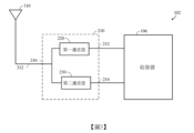
圖2顯示根據某些態樣之例示性頻率多工器210的方塊圖。在此實例中,頻率多工器210係包括第一埠212、第二埠214、及共用埠216的雙工器。然而,應理解,頻率多工器210不限於此實例。2 shows a block diagram of an exemplary frequency multiplexer 210 according to some aspects. In this example, the frequency multiplexer 210 is a duplexer including a first port 212, a second port 214, and a common port 216. However, it should be understood that the frequency multiplexer 210 is not limited to this example.

頻率多工器210包括耦接在第一埠212與共用埠216之間的第一濾波器220、及耦接在第二埠214與共用埠216之間的第二濾波器230。在某些態樣中,第一濾波器220經組態以傳遞第一頻帶中的信號,且第二濾波器230經組態以傳遞第二頻帶中的信號,其中第一頻帶及第二頻帶非重疊。第一濾波器220亦經組態以阻擋第二頻帶中的信號,且第二濾波器230經組態以阻擋第一頻帶中的信號。這允許頻率多工器210在共用埠216處接收第一頻帶及第二頻帶中的信號,且在第一埠212及第二埠214處分開信號。The frequency multiplexer 210 includes a first filter 220 coupled between the first port 212 and the common port 216, and a second filter 230 coupled between the second port 214 and the common port 216. In some aspects, the first filter 220 is configured to pass signals in a first frequency band, and the second filter 230 is configured to pass signals in a second frequency band, wherein the first frequency band and the second frequency band are non-overlapping. The first filter 220 is also configured to block signals in the second frequency band, and the second filter 230 is configured to block signals in the first frequency band. This allows the frequency multiplexer 210 to receive signals in the first frequency band and the second frequency band at the common port 216 and to separate the signals at the first port 212 and the second port 214.

在一個實例中,第一頻帶低於第二頻帶。在此實例中,第一濾波器220可使用低通濾波器來實施,且第二濾波器230可使用高通濾波器來實施。然而,應理解,頻率多工器210不限於此實例。In one example, the first frequency band is lower than the second frequency band. In this example, the first filter 220 may be implemented using a low pass filter, and the second filter 230 may be implemented using a high pass filter. However, it should be understood that the frequency multiplexer 210 is not limited to this example.

在操作中,頻率多工器210可經組態以在第一埠212處接收頻帶中的第一信號、在第二埠214處接收第二頻帶中的第二信號、並組合第一信號及第二信號。接著,頻率多工器210可經由共用埠216將經組合第一信號及第二信號輸出至共用通道(例如,共用傳輸線)。在此實例中,第一濾波器220(例如,低通濾波器)將第一頻帶中的第一信號從第一埠212傳遞至共用埠216,同時阻擋來自第一埠212的第二頻帶中的第二信號。此外,在此實例中,第二濾波器230(例如,高通濾波器)將第二頻帶中的第二信號從第二埠214傳遞至共用埠216,同時阻擋來自第二埠214的第一頻帶中的第一信號。In operation, the frequency multiplexer 210 may be configured to receive a first signal in a frequency band at a first port 212, receive a second signal in a second frequency band at a second port 214, and combine the first signal and the second signal. The frequency multiplexer 210 may then output the combined first and second signals to a common channel (e.g., a common transmission line) via a common port 216. In this example, a first filter 220 (e.g., a low-pass filter) passes the first signal in the first frequency band from the first port 212 to the common port 216 while blocking the second signal in the second frequency band from the first port 212. Furthermore, in this example, the second filter 230 (eg, a high pass filter) passes the second signal in the second frequency band from the second port 214 to the common port 216 while blocking the first signal in the first frequency band from the second port 214 .

頻率多工器210亦可經組態以在共用埠216處接收頻帶中的第一信號及第二頻帶中的第二信號,並使用濾波器220及230分離(即,分開)第一信號及第二信號。接著,頻率多工器210可在第一埠212處輸出第一信號,且在第二埠214處輸出第二信號。在此實例中,第一濾波器220(例如,低通濾波器)將第一頻帶中的第一信號從共用埠216傳遞至第一埠212,同時阻擋第二頻帶中的第二信號。此外,在此實例中,第二濾波器230(例如,高通濾波器)將第二頻帶中的第二信號從共用埠216傳遞至第二埠214,同時阻擋第一頻帶中的第一信號。The frequency multiplexer 210 may also be configured to receive a first signal in a frequency band and a second signal in a second frequency band at a common port 216 and separate (i.e., separate) the first signal and the second signal using filters 220 and 230. The frequency multiplexer 210 may then output the first signal at a first port 212 and the second signal at a second port 214. In this example, the first filter 220 (e.g., a low-pass filter) passes the first signal in the first frequency band from the common port 216 to the first port 212 while blocking the second signal in the second frequency band. Additionally, in this example, the second filter 230 (eg, a high pass filter) passes the second signal in the second frequency band from the common port 216 to the second port 214 while blocking the first signal in the first frequency band.

圖3顯示頻率多工器210的共用埠216經由傳輸線312(亦稱為饋線)耦接至天線310的實例。在此實例中,共用埠216亦可稱為天線埠,因為在此實例中共用埠216耦接至天線310。天線310可使用貼片天線、偶極天線、或另一類型的天線來實施。在此實例中,第一埠212及第二埠214耦接至收發器196。FIG3 shows an example in which the common port 216 of the frequency multiplexer 210 is coupled to the antenna 310 via a transmission line 312 (also referred to as a feeder). In this example, the common port 216 may also be referred to as an antenna port because in this example the common port 216 is coupled to the antenna 310. The antenna 310 may be implemented using a patch antenna, a dipole antenna, or another type of antenna. In this example, the first port 212 and the second port 214 are coupled to the transceiver 196.

在此實例中,頻率多工器210允許收發器196經由共用天線(即,天線310)傳輸及/或接收第一頻帶及第二頻帶中的信號。在一些實施方案中,收發器196可支援多種無線通訊技術,其中第一頻帶及第二頻帶用於無線通訊技術中的不同者。無線通訊技術可包括下列之二或更多者:第三代(third generation, 3G)技術(例如,CDMA)、第四代(fourth generation, 4G)技術(亦稱為長期演進(long term evolution, LTE))、第五代(fifth generation, 5G)技術、基於一或多個IEEE802.11協定(例如,IEEE 802.11ac、IEEE 802.11n、IEEE 802.11ad、IEEE 802.11ax、IEEE 802.11ay等)的一或多個技術、及/或一或多個其他技術。在其他實施方案中,第一頻帶及第二頻帶可用於相同的通訊技術。第一頻帶及/或第二頻帶可在毫米波(mmW)頻帶及/或另一頻帶中。mmW頻帶的實例包括第五代標準中使用的mmW頻帶。在一些實施方案中,第一頻帶及第二頻帶可在頻率範圍3 (FR3)(例如,7.125 GHz至24.250 GHz)中。In this example, the frequency multiplexer 210 allows the transceiver 196 to transmit and/or receive signals in the first frequency band and the second frequency band via a common antenna, i.e., the antenna 310. In some implementations, the transceiver 196 can support multiple wireless communication technologies, wherein the first frequency band and the second frequency band are used for different ones of the wireless communication technologies. The wireless communication technology may include two or more of the following: third generation (3G) technology (e.g., CDMA), fourth generation (4G) technology (also known as long term evolution (LTE)), fifth generation (5G) technology, one or more technologies based on one or more IEEE802.11 protocols (e.g., IEEE 802.11ac, IEEE 802.11n, IEEE 802.11ad, IEEE 802.11ax, IEEE 802.11ay, etc.), and/or one or more other technologies. In other embodiments, the first frequency band and the second frequency band may be used for the same communication technology. The first frequency band and/or the second frequency band may be in a millimeter wave (mmW) band and/or another frequency band. Examples of mmW bands include mmW bands used in fifth generation standards. In some implementations, the first and second bands may be in frequency range 3 (FR3) (eg, 7.125 GHz to 24.250 GHz).

為了傳輸第一頻帶中的第一信號(例如,第一射頻(RF)信號),收發器196可將第一信號輸出至頻率多工器210的第一埠212。頻率多工器210將第一頻帶中的第一信號傳遞至天線310,同時阻擋來自第二埠214的第一信號。為了傳輸第二頻帶中的第一信號(例如,第二RF信號),收發器196可將第二信號輸出至頻率多工器210的第二埠214。頻率多工器210將第二頻帶中的第二信號傳遞至天線310,同時阻擋來自第一埠212的第二信號。To transmit a first signal in a first frequency band (e.g., a first radio frequency (RF) signal), the transceiver 196 may output the first signal to the first port 212 of the frequency multiplexer 210. The frequency multiplexer 210 passes the first signal in the first frequency band to the antenna 310 while blocking the first signal from the second port 214. To transmit a first signal in a second frequency band (e.g., a second RF signal), the transceiver 196 may output a second signal to the second port 214 of the frequency multiplexer 210. The frequency multiplexer 210 passes the second signal in the second frequency band to the antenna 310 while blocking the second signal from the first port 212.

為了接收第一頻帶中的第一信號,頻率多工器210在共用埠216處接收來自天線310的第一信號,並經由第一埠212將第一信號傳遞至收發器196,同時阻擋來自第二埠214的第一信號。為了接收第二頻帶中的第二信號,頻率多工器210在共用埠216處接收來自天線310的第二信號,並經由第二埠214將第二信號傳遞至收發器196,同時阻擋來自第一埠212的第二信號。To receive a first signal in a first frequency band, the frequency multiplexer 210 receives a first signal from the antenna 310 at the common port 216 and transmits the first signal to the transceiver 196 via the first port 212 while blocking the first signal from the second port 214. To receive a second signal in a second frequency band, the frequency multiplexer 210 receives a second signal from the antenna 310 at the common port 216 and transmits the second signal to the transceiver 196 via the second port 214 while blocking the second signal from the first port 212.

圖4顯示根據某些態樣之收發器196的例示性實施方案。在此實例中,收發器196包括第一切換電路420、第一傳輸電路430、及第一接收電路435。第一切換電路420可使用單刀雙擲(single pole double throw, SP2T)開關或另一類型的開關來實施。第一切換電路420耦接至頻率多工器210的第一埠212、第一傳輸電路430、及第一接收電路435。第一切換電路420經組態以基於第一選擇信號選擇性地將第一傳輸電路430或第一接收電路435耦接至頻率多工器210的第一埠212。FIG. 4 shows an exemplary implementation of the transceiver 196 according to certain aspects. In this example, the transceiver 196 includes a first switching circuit 420, a first transmission circuit 430, and a first receiving circuit 435. The first switching circuit 420 can be implemented using a single pole double throw (SP2T) switch or another type of switch. The first switching circuit 420 is coupled to the first port 212 of the frequency multiplexer 210, the first transmission circuit 430, and the first receiving circuit 435. The first switching circuit 420 is configured to selectively couple the first transmission circuit 430 or the first receiving circuit 435 to the first port 212 of the frequency multiplexer 210 based on a first selection signal.

在此實例中,第一傳輸電路430可經組態以接收(例如,來自數據機194的)基頻信號或中頻(IF)信號、將基頻信號或IF信號處理成第一頻帶中的射頻(RF)信號、並將RF信號輸出至第一切換電路420。在此情況下,第一選擇信號可使第一切換電路420將RF信號耦接至頻率多工器210的第一埠212,以用於經由天線310傳輸。由第一傳輸電路430執行的處理可包括升頻轉換、濾波、放大、及類似者。第一頻帶中的RF信號可對應於上文討論之第一頻帶中的第一信號。In this example, the first transmission circuit 430 may be configured to receive a baseband signal or an intermediate frequency (IF) signal (e.g., from the modem 194), process the baseband signal or the IF signal into a radio frequency (RF) signal in a first frequency band, and output the RF signal to the first switching circuit 420. In this case, the first selection signal may cause the first switching circuit 420 to couple the RF signal to the first port 212 of the frequency multiplexer 210 for transmission via the antenna 310. The processing performed by the first transmission circuit 430 may include up-conversion, filtering, amplification, and the like. The RF signal in the first frequency band may correspond to the first signal in the first frequency band discussed above.

在此實例中,第一接收電路435可經組態以接收來自第一切換電路420之第一頻帶中的RF信號,並將RF信號處理成基頻信號或IF信號。在此情況下,第一選擇信號可使第一切換電路420將頻率多工器210的第一埠212耦接至第一接收電路435,使得第一接收電路435可透過頻率多工器210接收來自天線310的RF信號。由第一接收電路435執行的處理可包括降頻轉換、濾波、放大、及類似者。In this example, the first receiving circuit 435 may be configured to receive the RF signal in the first frequency band from the first switching circuit 420 and process the RF signal into a baseband signal or an IF signal. In this case, the first selection signal may cause the first switching circuit 420 to couple the first port 212 of the frequency multiplexer 210 to the first receiving circuit 435, so that the first receiving circuit 435 can receive the RF signal from the antenna 310 through the frequency multiplexer 210. The processing performed by the first receiving circuit 435 may include down-conversion, filtering, amplification, and the like.

在此實例中,收發器196亦包括第二切換電路440、第二傳輸電路450、及第二接收電路455。第二切換電路440可使用SP2T開關或另一類型的開關來實施。第二切換電路440耦接至頻率多工器210的第二埠214、第二傳輸電路450、及第二接收電路455。第二切換電路440經組態以基於第二選擇信號選擇性地將第二傳輸電路450或第二接收電路455耦接至頻率多工器210的第二埠214。In this example, the transceiver 196 also includes a second switching circuit 440, a second transmission circuit 450, and a second receiving circuit 455. The second switching circuit 440 can be implemented using an SP2T switch or another type of switch. The second switching circuit 440 is coupled to the second port 214 of the frequency multiplexer 210, the second transmission circuit 450, and the second receiving circuit 455. The second switching circuit 440 is configured to selectively couple the second transmission circuit 450 or the second receiving circuit 455 to the second port 214 of the frequency multiplexer 210 based on a second selection signal.

在此實例中,第二傳輸電路430可經組態以接收(例如,來自數據機194的)基頻信號或IF信號、將基頻信號或IF信號處理成第二頻帶中的RF信號、並將RF信號輸出至第二切換電路440。在此情況下,第二選擇信號可使第二切換電路440將RF信號耦接至頻率多工器210的第二埠214,以用於經由天線310傳輸。由第二傳輸電路450執行的處理可包括升頻轉換、濾波、放大、及類似者。第二頻帶中的RF信號可對應於上文討論之第二頻帶中的第二信號。In this example, the second transmission circuit 430 may be configured to receive a baseband signal or IF signal (e.g., from the modem 194), process the baseband signal or IF signal into an RF signal in a second frequency band, and output the RF signal to the second switching circuit 440. In this case, the second selection signal may cause the second switching circuit 440 to couple the RF signal to the second port 214 of the frequency multiplexer 210 for transmission via the antenna 310. The processing performed by the second transmission circuit 450 may include up-conversion, filtering, amplification, and the like. The RF signal in the second frequency band may correspond to the second signal in the second frequency band discussed above.

在此實例中,第二接收電路455可經組態以接收來自第一切換電路420之第二頻帶中的RF信號,並將RF信號處理成基頻信號或IF信號。在此情況下,第二選擇信號可使第二切換電路440將頻率多工器210的第二埠214耦接至第二接收電路455,使得第二接收電路455可透過頻率多工器210接收來自天線310的RF信號。由第二接收電路455執行的處理可包括降頻轉換、濾波、放大、及類似者。In this example, the second receiving circuit 455 may be configured to receive the RF signal in the second frequency band from the first switching circuit 420 and process the RF signal into a baseband signal or an IF signal. In this case, the second selection signal may cause the second switching circuit 440 to couple the second port 214 of the frequency multiplexer 210 to the second receiving circuit 455, so that the second receiving circuit 455 can receive the RF signal from the antenna 310 through the frequency multiplexer 210. The processing performed by the second receiving circuit 455 may include down-conversion, filtering, amplification, and the like.

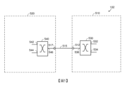
在某些態樣中,可使用頻率多工器為二或更多個模組提供頻域多工。在此方面,圖5顯示其中電子裝置102包括第一模組510及第二模組520的實例。在一些實施方案中,第一模組510係RF前端模組且第二模組520係IF模組。然而,應理解,本揭露不限於此實例。模組可包括一或多個晶片,其中模組的組件整合在一或多個晶片上。In some aspects, a frequency multiplexer can be used to provide frequency domain multiplexing for two or more modules. In this regard, FIG. 5 shows an example in which the electronic device 102 includes a first module 510 and a second module 520. In some embodiments, the first module 510 is an RF front-end module and the second module 520 is an IF module. However, it should be understood that the present disclosure is not limited to this example. The module may include one or more chips, wherein the components of the module are integrated on the one or more chips.

在此實例中,第一模組510包括第一頻率多工器530,且第二模組520包括第二頻率多工器540。頻率多工器530及540之各者可使用頻率多工器210的分開個例來實施。雖然圖5顯示模組510及520之各者包括一個頻率多工器(即,頻率多工器530及540之各別一者),但應理解,模組510及520之各者可包括多個頻率多工器。In this example, the first module 510 includes a first frequency multiplexer 530, and the second module 520 includes a second frequency multiplexer 540. Each of the frequency multiplexers 530 and 540 may be implemented using a separate instance of the frequency multiplexer 210. Although FIG. 5 shows each of the modules 510 and 520 including one frequency multiplexer (i.e., one of the frequency multiplexers 530 and 540), it should be understood that each of the modules 510 and 520 may include a plurality of frequency multiplexers.

在圖5中所示之實例中,第一頻率多工器530包括第一埠532、第二埠534、及共用埠536。對於第一頻率多工器530使用頻率多工器210的個例來實施的實例,第一埠532對應於第一埠212,第二埠534對應於第二埠214,且共用埠536對應於共用埠216。在此實例中,第一模組510包括耦接至共用埠536的介面512。介面512經組態以將共用埠536耦接至模組510與520之間的傳輸線515(例如,電纜、光纖等),如下文進一步討論。介面512可使用經組態以將第一模組510耦接至傳輸線515的任何結構來實施,包括墊、接腳、電纜或光纖連接器、及類似者。5 , the first frequency multiplexer 530 includes a first port 532, a second port 534, and a common port 536. For an example in which the first frequency multiplexer 530 is implemented using an instance of the frequency multiplexer 210, the first port 532 corresponds to the first port 212, the second port 534 corresponds to the second port 214, and the common port 536 corresponds to the common port 216. In this example, the first module 510 includes an interface 512 coupled to the common port 536. The interface 512 is configured to couple the common port 536 to a transmission line 515 (e.g., a cable, an optical fiber, etc.) between the modules 510 and 520, as discussed further below. The interface 512 may be implemented using any structure configured to couple the first module 510 to the transmission line 515, including pads, pins, cable or optical connectors, and the like.

第二頻率多工器540包括第一埠542、第二埠544、及共用埠546。對於第二頻率多工器540使用頻率多工器210的個例來實施的實例,第一埠542對應於第一埠212,第二埠544對應於第二埠214,且共用埠546對應於共用埠216。在此實例中,第二模組520包括耦接至共用埠546的介面517。s介面517經組態以將共用埠546耦接至傳輸線515。介面517可使用經組態以將第二模組520耦接至傳輸線515的任何結構來實施,包括墊、接腳、電纜或光纖連接器、及類似者。The second frequency multiplexer 540 includes a first port 542, a second port 544, and a common port 546. For an example in which the second frequency multiplexer 540 is implemented using an example of the frequency multiplexer 210, the first port 542 corresponds to the first port 212, the second port 544 corresponds to the second port 214, and the common port 546 corresponds to the common port 216. In this example, the second module 520 includes an interface 517 coupled to the common port 546. The interface 517 is configured to couple the common port 546 to the transmission line 515. The interface 517 can be implemented using any structure configured to couple the second module 520 to the transmission line 515, including pads, pins, cable or optical fiber connectors, and the like.

在此實例中,第一頻率多工器530及第二頻率多工器540允許第一模組510及第二模組520經由共用通道(即,傳輸線515)在第一頻帶及第二頻帶中彼此通訊。例如,第一頻率多工器530可在第一埠532處接收第一頻帶中的第一信號,且在第二埠534處接收第二頻帶中的第二信號。接著,第一頻率多工器530可經由共用埠536將第一信號及第二信號輸出至傳輸線515。第二頻率多工器540在共用埠546處接收第一信號及第二信號,分離(即,分開)第一信號及第二信號,在第一埠542處輸出第一信號,且在第二埠544處輸出第二信號。In this example, the first frequency multiplexer 530 and the second frequency multiplexer 540 allow the first module 510 and the second module 520 to communicate with each other in the first frequency band and the second frequency band via a common channel (i.e., transmission line 515). For example, the first frequency multiplexer 530 may receive a first signal in the first frequency band at a first port 532 and receive a second signal in the second frequency band at a second port 534. Then, the first frequency multiplexer 530 may output the first signal and the second signal to the transmission line 515 via a common port 536. The second frequency multiplexer 540 receives the first signal and the second signal at a common port 546, separates (i.e., separates) the first signal and the second signal, outputs the first signal at a first port 542, and outputs the second signal at a second port 544.

對於另一方向上的通訊,第二頻率多工器540可在第一埠542處接收第一頻帶中的第一信號,且在第二埠544處接收第二頻帶中的第二信號。接著,第二頻率多工器540可經由共用埠546將第一信號及第二信號輸出至傳輸線515。第一頻率多工器530在共用埠536處接收第一信號及第二信號,分離(即,分開)第一信號及第二信號,在第一埠532處輸出第一信號,且在第二埠534處輸出第二信號。For communication in the other direction, the second frequency multiplexer 540 may receive a first signal in a first frequency band at a first port 542 and a second signal in a second frequency band at a second port 544. The second frequency multiplexer 540 may then output the first signal and the second signal to the transmission line 515 via a common port 546. The first frequency multiplexer 530 receives the first signal and the second signal at a common port 536, separates (i.e., separates) the first signal and the second signal, outputs the first signal at a first port 532, and outputs the second signal at a second port 534.

圖6A顯示根據某些態樣之第一模組510包括RF前端電路系統且第二模組520包括IF電路系統的實例。在此實例中,第一模組510包括收發器602及控制電路606。收發器602耦接至第一頻率多工器530的第二埠534及一或多個天線610-1至610-n。控制電路606耦接至第一頻率多工器530的第一埠532。此外,在此實例中,第二模組520包括收發器604及控制電路608。收發器604耦接至第二頻率多工器540的第二埠544及數據機194。控制電路608耦接至第二頻率多工器540的第一埠542。收發器602及604可係收發器196的部分。FIG6A shows an example in which the first module 510 includes an RF front-end circuit system and the second module 520 includes an IF circuit system according to certain aspects. In this example, the first module 510 includes a transceiver 602 and a control circuit 606. The transceiver 602 is coupled to the second port 534 of the first frequency multiplexer 530 and one or more antennas 610-1 to 610-n. The control circuit 606 is coupled to the first port 532 of the first frequency multiplexer 530. In addition, in this example, the second module 520 includes a transceiver 604 and a control circuit 608. The transceiver 604 is coupled to the second port 544 of the second frequency multiplexer 540 and the modem 194. The control circuit 608 is coupled to the first port 542 of the second frequency multiplexer 540. Transceivers 602 and 604 may be part of transceiver 196 .

在操作中,收發器602可經組態經由一或多個天線610-1及610-n接收一或多個RF信號、將一或多個RF信號處理成第二頻帶中的IF信號、並將第二頻帶中的IF信號輸出至第一頻率多工器530的第二埠534。接著,第一頻率多工器530可經由傳輸線515將IF信號發送至第二模組520。由收發器602執行的處理可包括波束成形、從RF至IF的降頻轉換、放大、濾波、或其任何組合。第二頻率多工器540在共用埠546處接收第二頻帶中的IF信號,並經由第二埠544將該IF信號傳遞至收發器604。收發器604可經組態以將IF信號處理成基頻信號,並將基頻信號輸出至數據機194以用於進一步處理。由收發器604執行的處理可包括從IF至基頻的降頻轉換、濾波、放大、或其任何組合。In operation, the transceiver 602 may be configured to receive one or more RF signals via one or more antennas 610-1 and 610-n, process the one or more RF signals into an IF signal in a second frequency band, and output the IF signal in the second frequency band to the second port 534 of the first frequency multiplexer 530. The first frequency multiplexer 530 may then transmit the IF signal to the second module 520 via the transmission line 515. The processing performed by the transceiver 602 may include beamforming, down-conversion from RF to IF, amplification, filtering, or any combination thereof. The second frequency multiplexer 540 receives the IF signal in the second frequency band at the common port 546 and transmits the IF signal to the transceiver 604 via the second port 544. The transceiver 604 may be configured to process the IF signal into a baseband signal and output the baseband signal to the modem 194 for further processing. The processing performed by the transceiver 604 may include down-conversion from IF to baseband, filtering, amplification, or any combination thereof.

在另一方向上,收發器604可經組態接收來自數據機194的基頻信號、將基頻信號處理成第二頻帶中的IF信號、並將第二頻帶中的IF信號輸出至第二頻率多工器540的第二埠544。接著,第二頻率多工器540可經由傳輸線515將IF信號發送至第一模組510。由收發器604執行的處理可包括從基頻至IF的升頻轉換、放大、濾波、或其任何組合。第一頻率多工器530在共用埠536處接收第二頻帶中的IF信號,並經由第二埠534將該IF信號傳遞至收發器602。收發器602可經組態以將IF信號處理成一或多個RF信號,並將一或多個RF信號輸出至一或多個天線610-1至610-n以用於傳輸。由收發器602執行的處理可包括從IF至RF的升頻轉換、濾波、放大、波束成形(例如,以電子地操縱傳輸方向)、或其任何組合。In the other direction, the transceiver 604 can be configured to receive a baseband signal from the modem 194, process the baseband signal into an IF signal in a second frequency band, and output the IF signal in the second frequency band to the second port 544 of the second frequency multiplexer 540. The second frequency multiplexer 540 can then send the IF signal to the first module 510 via the transmission line 515. The processing performed by the transceiver 604 can include up-conversion from baseband to IF, amplification, filtering, or any combination thereof. The first frequency multiplexer 530 receives the IF signal in the second frequency band at the common port 536 and passes the IF signal to the transceiver 602 via the second port 534. The transceiver 602 may be configured to process the IF signal into one or more RF signals and output the one or more RF signals to one or more antennas 610-1 to 610-n for transmission. The processing performed by the transceiver 602 may include up-conversion from IF to RF, filtering, amplification, beamforming (e.g., to electronically steer the direction of transmission), or any combination thereof.

控制電路606及608可經組態以同步第一模組510與第二模組520之間的操作。為了進行這一點,控制電路606及608可經組態以經由傳輸線515彼此發送控制信號及/或時脈信號。控制信號及/或時脈信號係在低於第二頻帶的第一頻帶中。在此實例中,頻率多工器530及540能夠將第一頻帶中的控制信號及/或時脈信號與第二頻帶中的IF信號分開,允許控制信號及/或時脈信號及IF信號跨模組510與520之間的共用傳輸線(即,傳輸線515)發送。The control circuits 606 and 608 can be configured to synchronize the operations between the first module 510 and the second module 520. To do this, the control circuits 606 and 608 can be configured to send control signals and/or clock signals to each other via the transmission line 515. The control signals and/or clock signals are in a first frequency band that is lower than the second frequency band. In this example, the frequency multiplexers 530 and 540 can separate the control signals and/or clock signals in the first frequency band from the IF signals in the second frequency band, allowing the control signals and/or clock signals and the IF signals to be sent across the common transmission line (i.e., the transmission line 515) between the modules 510 and 520.

圖6B顯示根據某些態樣之第一模組510中之收發器602的例示性實施方案。在此實例中,收發器602包括波束成形器612,該波束成形器包括多個分支614-1至614-n,其中分支之各者耦接至天線610-1至610-n中的各別一者。分支614-1至614-n之各者包括各別的接收鏈,該接收鏈包括以鏈耦接的各別低雜訊放大器618-1至618-n、各別可變放大器620-1至620-n、及各別相移器622-1至622-n。分支614-1至614-n之各者亦包括各別的傳輸鏈,該傳輸鏈包括以鏈耦接的各別相移器624-1至624-n、各別可變放大器626-1至626-n、及各別功率放大器628-1至628-n。分支614-1至614-n之各者亦包括各別天線耦接器616-1至616-n,以用於將各別接收鏈及各別傳輸鏈耦接至天線610-1至610-n之各別一者。各別天線耦接器616-1至616-n可包括開關、雙工器(diplexer)、雙向器(duplexer)等。波束成形器612亦包括耦接至分支614-1至614-n中之接收鏈的功率組合器(power combiner) 630、及耦接至分支614-1至614-n中之傳輸鏈的功率分配器(power splitter) 632。功率組合器630經組態以將來自接收鏈的RF信號組合成經組合RF信號。功率分配器632經組態以將RF信號分成多個RF信號,並將RF信號之各者輸出至傳輸鏈之各別一者。6B shows an exemplary implementation of a transceiver 602 in the first module 510 according to certain aspects. In this example, the transceiver 602 includes a beamformer 612, which includes a plurality of branches 614-1 to 614-n, wherein each of the branches is coupled to a respective one of the antennas 610-1 to 610-n. Each of the branches 614-1 to 614-n includes a respective receiving chain, which includes a respective low-noise amplifier 618-1 to 618-n, a respective variable amplifier 620-1 to 620-n, and a respective phase shifter 622-1 to 622-n coupled in the chain. Each of the branches 614-1 to 614-n also includes a respective transmission chain, which includes a respective phase shifter 624-1 to 624-n, a respective variable amplifier 626-1 to 626-n, and a respective power amplifier 628-1 to 628-n coupled in a chain. Each of the branches 614-1 to 614-n also includes a respective antenna coupler 616-1 to 616-n for coupling the respective receiving chain and the respective transmission chain to a respective one of the antennas 610-1 to 610-n. The respective antenna couplers 616-1 to 616-n may include switches, diplexers, duplexers, etc. The beamformer 612 also includes a power combiner 630 coupled to the receive chains in the branches 614-1 to 614-n, and a power splitter 632 coupled to the transmit chains in the branches 614-1 to 614-n. The power combiner 630 is configured to combine the RF signals from the receive chains into a combined RF signal. The power splitter 632 is configured to split the RF signal into a plurality of RF signals and output each of the RF signals to a respective one of the transmit chains.

波束成形器612經組態以藉由使用相移器622-1至622-n對接收鏈中的RF信號施加不同的相移來電子地操縱天線610-1至610-n的接收波束。波束成形器612亦經組態以藉由使用相移器624-1至624-n對傳輸鏈中的RF信號施加不同的相移來電子地操縱天線610-1至610-n的傳輸波束。The beamformer 612 is configured to electronically steer the receive beams of the antennas 610-1 to 610-n by applying different phase shifts to the RF signals in the receive chain using the phase shifters 622-1 to 622-n. The beamformer 612 is also configured to electronically steer the transmit beams of the antennas 610-1 to 610-n by applying different phase shifts to the RF signals in the transmit chain using the phase shifters 624-1 to 624-n.

在此實例中,收發器602亦包括第一可變放大器634、第一正交產生器636、第一混頻器638、第二混頻器640、及第二可變放大器642。第一可變放大器634的輸入耦接至功率組合器630,且第一可變放大器634的輸出耦接至第一正交產生器636。第一混頻器638耦接在第一正交產生器636與第二可變放大器642的輸入之間。第二混頻器640耦接在第一正交產生器636與第二可變放大器642的輸入之間。在操作中,第一可變放大器634經組態以放大來自功率組合器630的經組合RF信號,且第一正交產生器636經組態以基於經放大組合RF信號來產生同相RF信號及正交RF信號、將同相RF信號輸出至第一混頻器638、並將正交RF信號輸出至第二混頻器640。第一混頻器638將同相RF信號與本地振盪器信號混頻,以將同相RF信號降頻轉換至同相IF信號。第二混頻器640將正交RF信號與本地振盪器信號混頻,以將正交RF信號降頻轉換至正交IF信號。同相IF信號及正交IF信號由第二可變放大器642組合並放大。In this example, the transceiver 602 also includes a first variable amplifier 634, a first quadrature generator 636, a first mixer 638, a second mixer 640, and a second variable amplifier 642. The input of the first variable amplifier 634 is coupled to the power combiner 630, and the output of the first variable amplifier 634 is coupled to the first quadrature generator 636. The first mixer 638 is coupled between the first quadrature generator 636 and the input of the second variable amplifier 642. The second mixer 640 is coupled between the first quadrature generator 636 and the input of the second variable amplifier 642. In operation, the first variable amplifier 634 is configured to amplify the combined RF signal from the power combiner 630, and the first quadrature generator 636 is configured to generate an in-phase RF signal and a quadrature RF signal based on the amplified combined RF signal, output the in-phase RF signal to the first mixer 638, and output the quadrature RF signal to the second mixer 640. The first mixer 638 mixes the in-phase RF signal with the local oscillator signal to down-convert the in-phase RF signal to the in-phase IF signal. The second mixer 640 mixes the quadrature RF signal with the local oscillator signal to down-convert the quadrature RF signal to the quadrature IF signal. The in-phase IF signal and the quadrature IF signal are combined and amplified by the second variable amplifier 642.

收發器602亦包括第三可變放大器644、第二正交產生器646、第三混頻器648、第四混頻器650、及第四可變放大器652。第三可變放大器644的輸入經組態以接收IF信號,且第三可變放大器644的輸出耦接至第二正交產生器646。第三混頻器648耦接在第二正交產生器646與第四可變放大器652的輸入之間。第四混頻器650耦接在第二正交產生器646與第四可變放大器652的輸入之間。在操作中,第三可變放大器644經組態以放大IF信號,且第二正交產生器646經組態以基於經放大IF信號來產生同相IF信號及正交IF信號、將同相IF信號輸出至第三混頻器648、並將正交IF信號輸出至第四混頻器650。第三混頻器648將同相IF信號與本地振盪器信號混頻,以將同相IF信號升頻轉換至同相RF信號。第四混頻器650將正交IF信號與本地振盪器信號混頻,以將正交IF信號升頻轉換至正交RF信號。同相RF信號及正交RF信號由第四可變放大器652組合並放大。第四可變放大器652的輸出耦接至功率分配器632以將經放大RF信號輸出至功率分配器632。The transceiver 602 also includes a third variable amplifier 644, a second quadrature generator 646, a third mixer 648, a fourth mixer 650, and a fourth variable amplifier 652. The input of the third variable amplifier 644 is configured to receive the IF signal, and the output of the third variable amplifier 644 is coupled to the second quadrature generator 646. The third mixer 648 is coupled between the second quadrature generator 646 and the input of the fourth variable amplifier 652. The fourth mixer 650 is coupled between the second quadrature generator 646 and the input of the fourth variable amplifier 652. In operation, the third variable amplifier 644 is configured to amplify the IF signal, and the second quadrature generator 646 is configured to generate an in-phase IF signal and a quadrature IF signal based on the amplified IF signal, output the in-phase IF signal to the third mixer 648, and output the quadrature IF signal to the fourth mixer 650. The third mixer 648 mixes the in-phase IF signal with the local oscillator signal to up-convert the in-phase IF signal to the in-phase RF signal. The fourth mixer 650 mixes the quadrature IF signal with the local oscillator signal to up-convert the quadrature IF signal to the quadrature RF signal. The in-phase RF signal and the quadrature RF signal are combined and amplified by the fourth variable amplifier 652. The output of the fourth variable amplifier 652 is coupled to the power divider 632 to output the amplified RF signal to the power divider 632 .

在此實例中,收發器602亦可包括切換電路654,該切換電路耦接至第二可變放大器642的輸出、第三可變放大器644的輸入、及頻率多工器530的第二埠534(示於圖6A中)。切換電路654可包括SP2T開關或另一類型的開關,以用於將頻率多工器530的第二埠534選擇性地耦接至第二可變放大器642的輸出或第三可變放大器644的輸入。In this example, the transceiver 602 may also include a switching circuit 654 coupled to the output of the second variable amplifier 642, the input of the third variable amplifier 644, and the second port 534 (shown in FIG. 6A ) of the frequency multiplexer 530. The switching circuit 654 may include an SP2T switch or another type of switch for selectively coupling the second port 534 of the frequency multiplexer 530 to the output of the second variable amplifier 642 or the input of the third variable amplifier 644.

圖6C顯示根據某些態樣之第二模組520中之收發器604的例示性實施方案。在此實例中,收發器604包括放大器658、耦接在數據機194與放大器658的輸入之間的第一傳輸鏈、及耦接在數據機194與放大器658的輸入之間的第二傳輸鏈。第一傳輸鏈包括以鏈耦接的第一數位轉類比轉換器(digital-to-analog converter, DAC) 666、第一濾波器664、第一可變放大器662、及第一混頻器660。第一DAC 666經組態以將來自數據機194的數位基頻信號轉換成類比基頻信號,第一濾波器664經組態以濾波基頻信號,第一可變放大器662經組態以放大基頻信號,且第一混頻器660經組態以將基頻信號與同相本地振盪器信號混頻,以將基頻信號升頻轉換至同相IF信號。6C shows an exemplary implementation of the transceiver 604 in the second module 520 according to certain aspects. In this example, the transceiver 604 includes an amplifier 658, a first transmission chain coupled between the modem 194 and the input of the amplifier 658, and a second transmission chain coupled between the modem 194 and the input of the amplifier 658. The first transmission chain includes a first digital-to-analog converter (DAC) 666, a first filter 664, a first variable amplifier 662, and a first mixer 660 coupled in the chain. The first DAC 666 is configured to convert the digital baseband signal from the modem 194 into an analog baseband signal, the first filter 664 is configured to filter the baseband signal, the first variable amplifier 662 is configured to amplify the baseband signal, and the first mixer 660 is configured to mix the baseband signal with an in-phase local oscillator signal to up-convert the baseband signal to an in-phase IF signal.

第二傳輸鏈包括以一鏈耦接的第二DAC 668、第二濾波器670、第二可變放大器672、及第二混頻器674。第二DAC 668經組態以將來自數據機194的數位基頻信號轉換成類比基頻信號,第二濾波器670經組態以濾波基頻信號,第二可變放大器672經組態以放大基頻信號,且第二混頻器674經組態以將基頻信號與正交本地振盪器信號混頻,以將基頻信號升頻轉換至正交IF信號。正交本地振盪器信號可與同相本地振盪器信號異相90度。來自混頻器660及674的同相IF信號及正交IF信號由放大器658組合並放大。The second transmission chain includes a second DAC 668, a second filter 670, a second variable amplifier 672, and a second mixer 674 coupled in a chain. The second DAC 668 is configured to convert the digital baseband signal from the modem 194 into an analog baseband signal, the second filter 670 is configured to filter the baseband signal, the second variable amplifier 672 is configured to amplify the baseband signal, and the second mixer 674 is configured to mix the baseband signal with the quadrature local oscillator signal to upconvert the baseband signal into a quadrature IF signal. The quadrature local oscillator signal may be 90 degrees out of phase with the in-phase local oscillator signal. The in-phase IF signal and the quadrature IF signal from mixers 660 and 674 are combined and amplified by amplifier 658.

收發器604亦包括經組態以接收IF信號並放大IF信號的放大器676、耦接在放大器676的輸出與數據機194之間的第一接收鏈、及耦接在放大器676的輸出與數據機之間的第二接收鏈。The transceiver 604 also includes an amplifier 676 configured to receive and amplify the IF signal, a first receive chain coupled between the output of the amplifier 676 and the modem 194, and a second receive chain coupled between the output of the amplifier 676 and the modem.

第一接收鏈包括以鏈耦接的第三混頻器678、第三可變放大器680、第三濾波器682、及第一類比轉數位轉換器(analog-to-digital converter, ADC) 684。第三混頻器678經組態以將IF信號與同相本地振盪器信號混頻,以將IF信號降頻轉換至同相基頻信號,第三可變放大器680經組態以放大同相基頻信號,第三濾波器682經組態以濾波同相基頻信號,且第一ADC 684經組態以將同相基頻信號轉換成數位信號並將數位信號輸出至數據機194。The first receiving chain includes a third mixer 678, a third variable amplifier 680, a third filter 682, and a first analog-to-digital converter (ADC) 684 coupled in the chain. The third mixer 678 is configured to mix the IF signal with the in-phase local oscillator signal to down-convert the IF signal to an in-phase baseband signal, the third variable amplifier 680 is configured to amplify the in-phase baseband signal, the third filter 682 is configured to filter the in-phase baseband signal, and the first ADC 684 is configured to convert the in-phase baseband signal into a digital signal and output the digital signal to the modem 194.

第二接收鏈包括以鏈耦接的第四混頻器692、第四可變放大器690、第四濾波器688、及第二ADC 686。第四混頻器692經組態以將IF信號與正交本地振盪器信號混頻,以將IF信號降頻轉換至正交基頻信號,第四可變放大器690經組態以放大正交基頻信號,第四濾波器688經組態以濾波正交基頻信號,且第二ADC 686經組態以將正交基頻信號轉換成數位信號並將數位信號輸出至數據機。The second receiving chain includes a fourth mixer 692, a fourth variable amplifier 690, a fourth filter 688, and a second ADC 686 coupled in a chain. The fourth mixer 692 is configured to mix the IF signal with the quadrature local oscillator signal to down-convert the IF signal to a quadrature baseband signal, the fourth variable amplifier 690 is configured to amplify the quadrature baseband signal, the fourth filter 688 is configured to filter the quadrature baseband signal, and the second ADC 686 is configured to convert the quadrature baseband signal into a digital signal and output the digital signal to the modem.

在此實例中,收發器604亦可包括切換電路656,該切換電路耦接至放大器658的輸出、放大器676的輸入、及頻率多工器540的第二埠544(示於圖6A中)。切換電路656可包括SP2T開關或另一類型的開關,以用於將頻率多工器540的第二埠544選擇性地耦接至放大器658的輸出或放大器676的輸入。In this example, the transceiver 604 may also include a switching circuit 656 coupled to the output of the amplifier 658, the input of the amplifier 676, and the second port 544 (shown in FIG. 6A ) of the frequency multiplexer 540. The switching circuit 656 may include an SP2T switch or another type of switch for selectively coupling the second port 544 of the frequency multiplexer 540 to the output of the amplifier 658 or the input of the amplifier 676.

應理解,收發器602及604不限於圖6B及圖6C中所示之例示性實施方案。It should be understood that transceivers 602 and 604 are not limited to the exemplary implementations shown in Figures 6B and 6C.

返回圖2,頻率多工器210的第一濾波器220及第二濾波器230可包括電感器及電容器(例如,電感器電容器(LC網路)。在此方面,圖7顯示根據某些態樣之第一濾波器220及第二濾波器230的例示性實施方案。在此實例中,第一濾波器220包括電感器710及電容器720。電感器710耦接在共用埠216與第一埠212之間,其中電感器710的第一端子712耦接至共用埠216且電感器710的第二端子714耦接至第一埠212。電容器720耦接在共用埠216與接地(或某個參考電位)之間。在圖7中所示之實例中,第一濾波器220實施低通(LP)濾波器。Returning to FIG. 2 , the first filter 220 and the second filter 230 of the frequency multiplexer 210 may include an inductor and a capacitor (e.g., an inductor capacitor (LC network). In this regard, FIG. 7 shows an exemplary implementation of the first filter 220 and the second filter 230 according to certain aspects. In this example, the first filter 220 includes an inductor 710 and a capacitor 720. The inductor 710 is coupled between the common port 216 and the first port 212, wherein the first terminal 712 of the inductor 710 is coupled to the common port 216 and the second terminal 714 of the inductor 710 is coupled to the first port 212. The capacitor 720 is coupled between the common port 216 and ground (or a reference potential). In the example shown in FIG. 7 , the first filter 220 implements a low-pass (LP) filter.

應理解,第一濾波器220不限於圖7中所示之例示性實施方案。例如,在一些實施方案中,電容器720可移動至電感器710的另一側。在另一實例中,第一濾波器220可包括耦接至電感器710之另一側的第二電容器。It should be understood that the first filter 220 is not limited to the exemplary embodiment shown in FIG7. For example, in some embodiments, the capacitor 720 can be moved to the other side of the inductor 710. In another example, the first filter 220 can include a second capacitor coupled to the other side of the inductor 710.

在圖7中所示之實例中,第二濾波器230包括第一電容器740、第二電容器750、及電感器730。在此實例中,第一電容器740耦接在共用埠216與電感器730的第一端子732之間,第二電容器750耦接在電感器730的第一端子732與第二埠214之間,且電感器730的第二端子734耦接至接地(或某個參考電位)。在圖7中所示之實例中,第二濾波器230實施高通(HP)濾波器。In the example shown in FIG7 , the second filter 230 includes a first capacitor 740, a second capacitor 750, and an inductor 730. In this example, the first capacitor 740 is coupled between the common port 216 and the first terminal 732 of the inductor 730, the second capacitor 750 is coupled between the first terminal 732 of the inductor 730 and the second port 214, and the second terminal 734 of the inductor 730 is coupled to ground (or a reference potential). In the example shown in FIG7 , the second filter 230 implements a high pass (HP) filter.

應理解,第二濾波器230不限於圖7中所示之例示性實施方案。例如,在一些實施方案中,可省略電容器740及750之一者。It should be understood that the second filter 230 is not limited to the exemplary embodiment shown in Figure 7. For example, in some embodiments, one of the capacitors 740 and 750 may be omitted.

在頻率多工器(例如,頻率多工器210)中使用電感器的挑戰在於,電感器可能佔據晶片或基材的大面積,使得難以減小頻率多工器的大小。LP濾波器(例如,第一濾波器220)中之電感器(例如,電感器710)的電感可遠大於HP濾波器(例如,第二濾波器230)中之電感器(例如,電感器730)的電感,且因此可對頻率多工器的大小具有較大影響。因此,欲減小第一濾波器220中之電感器710的面積,同時仍達成低通濾波所需的電感,以減小頻率多工器210的大小。A challenge with using inductors in a frequency multiplexer (e.g., frequency multiplexer 210) is that the inductors may occupy a large area of a chip or substrate, making it difficult to reduce the size of the frequency multiplexer. The inductance of an inductor (e.g., inductor 710) in an LP filter (e.g., first filter 220) may be much greater than the inductance of an inductor (e.g., inductor 730) in an HP filter (e.g., second filter 230), and therefore may have a greater impact on the size of the frequency multiplexer. Therefore, it is desirable to reduce the area of inductor 710 in first filter 220 while still achieving the inductance required for low pass filtering in order to reduce the size of frequency multiplexer 210.

另一挑戰在於第一濾波器220中之電感器710可能發射第一頻帶中的信號之頻率的諧波下的電磁干擾(亦稱為諧波發射)。諧波可在第二頻帶內。因此,來自電感器710的諧波發射可能使在第二頻帶中操作之組件(例如,第二濾波器230、收發器602中的組件等)的效能降級。因此,欲減少來自電感器710的諧波發射。Another challenge is that the inductor 710 in the first filter 220 may emit electromagnetic interference at harmonics of the frequency of the signal in the first frequency band (also referred to as harmonic emission). The harmonics may be in the second frequency band. Therefore, the harmonic emission from the inductor 710 may degrade the performance of components operating in the second frequency band (e.g., the second filter 230, components in the transceiver 602, etc.). Therefore, it is desirable to reduce the harmonic emission from the inductor 710.

為了處理上述,本揭露之態樣提供包括電感器堆疊的三維電感器結構。將電感器堆疊允許電感器結構在較小的面積內達成給定電感。在某些態樣中,電感器形成偶極電感器及/或四極電感器,其等將電感器的磁場集中在電感器結構內。這使電感器的磁場在電感器結構外部快速地減弱,且因此減少來自電感器結構的諧波發射。下文進一步討論電感器結構的上述特徵及其他特徵。To address the above, aspects of the present disclosure provide a three-dimensional inductor structure including a stack of inductors. Stacking the inductors allows the inductor structure to achieve a given inductance within a smaller area. In certain aspects, the inductors form dipole inductors and/or quadrupole inductors, which concentrate the magnetic field of the inductor within the inductor structure. This causes the magnetic field of the inductor to decay rapidly outside the inductor structure and, therefore, reduces harmonic emission from the inductor structure. The above features and other features of the inductor structure are discussed further below.

圖8顯示根據本揭露之態樣的圖7中所示之電感器710使用電感器結構810來實施的實例。電感器結構810具有第一端子812(亦稱為第一埠)及第二端子814(亦稱為第二埠)。在圖8中所示之實例中,第一端子812耦接至共用埠216且第二端子814耦接至第一埠212。FIG8 shows an example of an inductor structure 810 used to implement the inductor 710 shown in FIG7 according to aspects of the present disclosure. The inductor structure 810 has a first terminal 812 (also referred to as a first port) and a second terminal 814 (also referred to as a second port). In the example shown in FIG8, the first terminal 812 is coupled to the common port 216 and the second terminal 814 is coupled to the first port 212.

圖9顯示電感器結構810之例示性實施方案的電路示意圖。在此實例中,電感器結構810包括第一端子812與第二端子814之間的導體路徑905。導體路徑905包括第一偶極電感器910及第二偶極電感器915。如本文所使用,偶極電感器包括兩個電感器(例如,螺旋電感器或迴路電感器),該兩個電感器由於其中流動的相對電流而具有相對的磁場極性。例如,電流可在兩個電感器之一者中以順時針方向流動,且在兩個電感器中之另一者中以逆時針方向流動。在圖9中的實例中,導體路徑905從第一端子812連續至第二端子814。FIG9 shows a circuit diagram of an exemplary embodiment of an inductor structure 810. In this example, the inductor structure 810 includes a conductor path 905 between a first terminal 812 and a second terminal 814. The conductor path 905 includes a first dipole inductor 910 and a second dipole inductor 915. As used herein, a dipole inductor includes two inductors (e.g., spiral inductors or loop inductors) that have opposite magnetic field polarities due to opposite currents flowing therein. For example, current may flow in a clockwise direction in one of the two inductors and in a counterclockwise direction in the other of the two inductors. In the example in FIG9 , the conductor path 905 continues from the first terminal 812 to the second terminal 814.

第一偶極電感器910包括第一電感器920及第二電感器930,且第二偶極電感器915包括第三電感器940及第四電感器950。在某些態樣中,第一電感器920及第二電感器930由第一金屬層形成,且第三電感器940及第四電感器950由第一金屬層上方的第二金屬層形成。這允許第二偶極電感器915堆疊在第一偶極電感器910之上以用於較緊湊的結構,如下文進一步討論。First dipole inductor 910 includes first inductor 920 and second inductor 930, and second dipole inductor 915 includes third inductor 940 and fourth inductor 950. In certain aspects, first inductor 920 and second inductor 930 are formed from a first metal layer, and third inductor 940 and fourth inductor 950 are formed from a second metal layer above the first metal layer. This allows second dipole inductor 915 to be stacked on top of first dipole inductor 910 for a more compact structure, as discussed further below.

在圖9中所示之實例中,第一電感器920耦接在第一端子812與第三電感器940之間,第三電感器940耦接在第一電感器920與第二電感器930之間,且第四電感器950耦接在第二電感器930與第二端子814之間。因此,導體路徑905在第一偶極電感器910中的電感器920及930與第二偶極電感器915中的電感器940及950之間交替。例如,當電流通過導體路徑905從第一端子812流動至第二端子814時,電流以下列順序流動通過電感器920、930、940、及950:第一金屬層中的第一電感器920、第二金屬層中的第三電感器940、第一金屬層中的第二電感器930、及第二金屬層中的第四電感器950。9 , the first inductor 920 is coupled between the first terminal 812 and the third inductor 940, the third inductor 940 is coupled between the first inductor 920 and the second inductor 930, and the fourth inductor 950 is coupled between the second inductor 930 and the second terminal 814. Thus, the conductive path 905 alternates between the inductors 920 and 930 in the first dipole inductor 910 and the inductors 940 and 950 in the second dipole inductor 915. For example, when current flows from the first terminal 812 to the second terminal 814 through the conductive path 905, the current flows through the inductors 920, 930, 940, and 950 in the following order: the first inductor 920 in the first metal layer, the third inductor 940 in the second metal layer, the second inductor 930 in the first metal layer, and the fourth inductor 950 in the second metal layer.

在第一金屬層中的電感器920及930與第二金屬層中的電感器940及950之間交替減少電感器結構810中的電感器920、930、940、與950之間的電容耦接。較低的電容耦接允許電感器結構810達成較高的自諧振頻率。較高的自諧振頻率增加第二頻帶中之信號所經歷的第一濾波器220的阻抗,這減少第二頻帶中之信號的插入損耗且幫助將第一埠212與第二頻帶中的信號隔離。Alternating between inductors 920 and 930 in the first metal layer and inductors 940 and 950 in the second metal layer reduces the capacitive coupling between inductors 920, 930, 940, and 950 in inductor structure 810. Lower capacitive coupling allows inductor structure 810 to achieve a higher self-resonant frequency. The higher self-resonant frequency increases the impedance of first filter 220 seen by signals in the second frequency band, which reduces insertion loss for signals in the second frequency band and helps isolate first port 212 from signals in the second frequency band.

圖10A顯示圖9中之電感器920、930、940、及950的例示性實施方案的透視圖。在此實例中,電感器920、930、940、及950之各者使用各別螺旋電感器來實施。應理解,各螺旋電感器可具有比圖10A中所示之實例更少的匝數或更多的匝數。FIG10A shows a perspective view of an exemplary implementation of inductors 920, 930, 940, and 950 in FIG9. In this example, each of inductors 920, 930, 940, and 950 is implemented using a respective spiral inductor. It should be understood that each spiral inductor may have fewer turns or more turns than the example shown in FIG10A.

在此實例中,第一電感器920及第二電感器930由第一金屬層形成(例如,使用微影及蝕刻程序)。第一金屬層可在基材(例如,矽基材、層壓體、低溫共燒陶瓷(low temperature co-fired ceramic)、雙馬來醯亞胺-三𠯤(BT))、PCB等)上且/或嵌入該基材中。圖10B顯示第一電感器920及第二電感器930的俯視圖。在一些實施方案中,第一電感器920及第二電感器930之各者係平面電感器(例如,平面螺旋電感器)。如本文所使用,平面電感器係由平坦金屬層(例如,第一金屬層)形成的電感器。如圖10B中所示,第一電感器920在第一金屬層中相鄰於第二電感器930。In this example, the first inductor 920 and the second inductor 930 are formed from a first metal layer (e.g., using lithography and etching processes). The first metal layer may be on a substrate (e.g., a silicon substrate, a laminate, a low temperature co-fired ceramic, bismaleimide-tris(BT), a PCB, etc.) and/or embedded in the substrate. FIG. 10B shows a top view of the first inductor 920 and the second inductor 930. In some embodiments, each of the first inductor 920 and the second inductor 930 is a planar inductor (e.g., a planar spiral inductor). As used herein, a planar inductor is an inductor formed from a flat metal layer (e.g., a first metal layer). As shown in FIG. 10B , the first inductor 920 is adjacent to the second inductor 930 in the first metal layer.

在此實例中,第三電感器940及第四電感器950由第一金屬層上方的第二金屬層形成(例如,使用微影及蝕刻程序)。第二金屬層可在基材(例如,矽基材、層壓體、低溫共燒陶瓷、雙馬來醯亞胺-三𠯤(BT))、PCB等)上且/或嵌入該基材中。圖10C顯示第三電感器940及第四電感器950的俯視圖。在一些實施方案中,第三電感器940及第四電感器950之各者係平面電感器(例如,平面螺旋電感器)。如圖10C中所示,第三電感器940在第二金屬層中相鄰於第四電感器950。In this example, the third inductor 940 and the fourth inductor 950 are formed by a second metal layer above the first metal layer (e.g., using lithography and etching processes). The second metal layer can be on a substrate (e.g., a silicon substrate, a laminate, a low temperature co-fired ceramic, bismaleimide-tris(BT), a PCB, etc.) and/or embedded in the substrate. FIG. 10C shows a top view of the third inductor 940 and the fourth inductor 950. In some embodiments, each of the third inductor 940 and the fourth inductor 950 is a planar inductor (e.g., a planar spiral inductor). As shown in FIG. 10C, the third inductor 940 is adjacent to the fourth inductor 950 in the second metal layer.

在此實例中,電感器結構810的導體路徑905亦包括第一通孔1010、第二通孔1020、及第三通孔1030。第一通孔1010設置在第一電感器920與第三電感器940之間,且將第一電感器920耦接至第三電感器940。第二通孔1020設置在第二電感器930與第三電感器940之間,且將第二電感器930耦接至第三電感器940。第三通孔1030設置在第二電感器930與第四電感器950之間,且將第二電感器930耦接至第四電感器950。請注意,圖10A顯示電感器結構810的分解圖,以更清楚地顯示通孔1010、1020、及1030。In this example, the conductive path 905 of the inductor structure 810 also includes a first through-hole 1010, a second through-hole 1020, and a third through-hole 1030. The first through-hole 1010 is disposed between the first inductor 920 and the third inductor 940, and couples the first inductor 920 to the third inductor 940. The second through-hole 1020 is disposed between the second inductor 930 and the third inductor 940, and couples the second inductor 930 to the third inductor 940. The third through-hole 1030 is disposed between the second inductor 930 and the fourth inductor 950, and couples the second inductor 930 to the fourth inductor 950. Note that FIG. 10A shows an exploded view of the inductor structure 810 to more clearly show the through-holes 1010, 1020, and 1030.

在圖10A中的實例中,第一偶極電感器910的第一電感器920及第二電感器930重疊第二偶極電感器915的第三電感器940及第四電感器950。這允許第二偶極電感器915堆疊在第一偶極電感器910之上以在晶片或基材的較小面積中達成給定電感。10A, first inductor 920 and second inductor 930 of first dipole inductor 910 overlap third inductor 940 and fourth inductor 950 of second dipole inductor 915. This allows second dipole inductor 915 to be stacked on top of first dipole inductor 910 to achieve a given inductance in a smaller area of a chip or substrate.

在此實例中,導體路徑905經組態以使得電流在第一偶極電感器910的第一電感器920及第二電感器940中以相對方向流動。圖10A包括對於電流在導體路徑905中從第一端子812流動至第二端子814的情況下,顯示第一電感器920中之電流方向及第二電感器930中之電流方向的箭頭。在此實例中,電流在第一電感器920中以順時針方向流動,且在第二電感器930中以逆時針方向流動。相對的電流流動使第一電感器920及第二電感器930具有相對的磁場極性,這導致第一電感器920與第二電感器930之間的強磁耦接。In this example, the conductor path 905 is configured so that current flows in opposite directions in the first inductor 920 and the second inductor 940 of the first dipole inductor 910. FIG. 10A includes arrows showing the direction of current in the first inductor 920 and the direction of current in the second inductor 930 for a current flowing from the first terminal 812 to the second terminal 814 in the conductor path 905. In this example, the current flows in the first inductor 920 in a clockwise direction and in the second inductor 930 in a counterclockwise direction. The opposite current flows cause the first inductor 920 and the second inductor 930 to have opposite magnetic field polarities, which results in a strong magnetic coupling between the first inductor 920 and the second inductor 930.

導體路徑905亦經組態以使得電流在第二偶極電感器915的第三電感器940及第四電感器950中以相對方向流動。圖10A包括對於電流在導體路徑905中從第一端子812流動至第二端子814的情況下,顯示第三電感器940中之電流方向及第四電感器950中之電流方向的箭頭。在此實例中,電流在第三電感器940中以順時針方向流動,且在第四電感器950中以逆時針方向流動。相對的電流流動使第三電感器940及第四電感器950具有相對的磁場極性,這導致第三電感器940與第四電感器950之間的強磁耦接。The conductive path 905 is also configured so that current flows in opposite directions in the third inductor 940 and the fourth inductor 950 of the second dipole inductor 915. FIG. 10A includes arrows showing the direction of current in the third inductor 940 and the direction of current in the fourth inductor 950 for a case where current flows in the conductive path 905 from the first terminal 812 to the second terminal 814. In this example, current flows in a clockwise direction in the third inductor 940 and in a counterclockwise direction in the fourth inductor 950. The opposite current flows cause the third inductor 940 and the fourth inductor 950 to have opposite magnetic field polarities, which results in strong magnetic coupling between the third inductor 940 and the fourth inductor 950.

因此,在此實例中,電感器結構810包括偶極電感器堆疊,該偶極電感器堆疊包括第一偶極電感器910及第二偶極電感器915,其中第二偶極電感器915重疊第一偶極電感器910且堆疊在該第一偶極電感器之上。偶極電感器910及915將電感器結構810的磁場集中在電感器結構810內。因此,磁場在電感器結構810外部快速地減弱,這減少來自電感器結構810的諧波發射及磁發射。Thus, in this example, inductor structure 810 includes a dipole inductor stack including a first dipole inductor 910 and a second dipole inductor 915, wherein second dipole inductor 915 overlaps and is stacked on top of first dipole inductor 910. Dipole inductors 910 and 915 concentrate the magnetic field of inductor structure 810 within inductor structure 810. Thus, the magnetic field rapidly decays outside inductor structure 810, which reduces harmonic emission and magnetic emission from inductor structure 810.

應理解,可將額外的偶極電感器堆疊以增加給定面積的電感。在此方面,圖11顯示電感器結構810的導體路徑905包括第三偶極電感器1110及第四偶極電感器1115的實例。第三偶極電感器1110包括第五電感器1120及第六電感器1130,且第四偶極電感器1156包括第七電感器1140及第八電感器1150。在某些態樣中,第五電感器1120及第六電感器1130由第三金屬層形成,且第七電感器1140及第八電感器1150由第三金屬層上方的第四金屬層形成(例如,使用微影及蝕刻程序)。第三金屬層在上文討論之第二金屬層上方。It should be understood that additional dipole inductors may be stacked to increase the inductance for a given area. In this regard, FIG. 11 shows an example where the conductive path 905 of the inductor structure 810 includes a third dipole inductor 1110 and a fourth dipole inductor 1115. The third dipole inductor 1110 includes a fifth inductor 1120 and a sixth inductor 1130, and the fourth dipole inductor 1156 includes a seventh inductor 1140 and an eighth inductor 1150. In some aspects, the fifth inductor 1120 and the sixth inductor 1130 are formed from a third metal layer, and the seventh inductor 1140 and the eighth inductor 1150 are formed from a fourth metal layer above the third metal layer (e.g., using a lithography and etching process). The third metal layer is above the second metal layer discussed above.

在此實例中,第五電感器1120耦接在第四電感器950與第七電感器1140之間,第七電感器1140耦接在第五電感器1120與第六電感器1130之間,第六電感器1130耦接在第七電感器1140與第八電感器1150之間,且第八電感器1150耦接在第六電感器1130與第二端子814之間。因此,導體路徑905在第三偶極電感器1110中的電感器1120及1130與第四偶極電感器1115中的電感器1140及1150之間交替。如上文所討論,在不同金屬層中之電感器之間交替減少三維(3D)分布磁偶極電感器之間的電容耦接,這允許電感器結構810達成較高的自諧振頻率。較高的自諧振頻率增加第二頻帶中之信號所經歷的第一濾波器220的阻抗,這減少第二頻帶中之信號的插入損耗且幫助將第一埠212與第二頻帶中的信號隔離。In this example, the fifth inductor 1120 is coupled between the fourth inductor 950 and the seventh inductor 1140, the seventh inductor 1140 is coupled between the fifth inductor 1120 and the sixth inductor 1130, the sixth inductor 1130 is coupled between the seventh inductor 1140 and the eighth inductor 1150, and the eighth inductor 1150 is coupled between the sixth inductor 1130 and the second terminal 814. Thus, the conductive path 905 alternates between the inductors 1120 and 1130 in the third dipole inductor 1110 and the inductors 1140 and 1150 in the fourth dipole inductor 1115. As discussed above, alternating between inductors in different metal layers reduces capacitive coupling between three-dimensional (3D) distributed magnetic dipole inductors, which allows the inductor structure 810 to achieve a higher self-resonance frequency. The higher self-resonance frequency increases the impedance of the first filter 220 seen by signals in the second frequency band, which reduces insertion loss of signals in the second frequency band and helps isolate the first port 212 from signals in the second frequency band.

圖12A顯示圖11中之電感器1120、1130、1140、及1150的例示性實施方案的透視圖。在此實例中,電感器1120、1130、1140、及1150之各者使用各別螺旋電感器來實施。應理解,各螺旋電感器可具有比圖12A中所示之實例更少的匝數或更多的匝數。FIG12A shows a perspective view of an exemplary implementation of inductors 1120, 1130, 1140, and 1150 in FIG11. In this example, each of inductors 1120, 1130, 1140, and 1150 is implemented using a respective spiral inductor. It should be understood that each spiral inductor may have fewer turns or more turns than the example shown in FIG12A.

在此實例中,第五電感器1120及第六電感器1130由第三金屬層形成(例如,使用微影及蝕刻程序)。第三金屬層可在基材(例如,矽基材、層壓體、低溫共燒陶瓷、雙馬來醯亞胺-三𠯤(BT))、PCB等)上且/或嵌入該基材中。如圖12A中所示,第三金屬層在第一金屬層及第二金屬層上方。圖12B顯示第五電感器1120及第六電感器1130的俯視圖。在一些實施方案中,第五電感器1120及第六電感器1130之各者係平面電感器(例如,平面螺旋電感器)。In this example, the fifth inductor 1120 and the sixth inductor 1130 are formed by a third metal layer (e.g., using lithography and etching processes). The third metal layer may be on a substrate (e.g., a silicon substrate, a laminate, a low temperature co-fired ceramic, bismaleimide-tris(BT), a PCB, etc.) and/or embedded in the substrate. As shown in FIG. 12A, the third metal layer is above the first metal layer and the second metal layer. FIG. 12B shows a top view of the fifth inductor 1120 and the sixth inductor 1130. In some embodiments, each of the fifth inductor 1120 and the sixth inductor 1130 is a planar inductor (e.g., a planar spiral inductor).

在此實例中,第七電感器1140及第八電感器1150由第三金屬層上方的第四金屬層形成(例如,使用微影及蝕刻程序)。第四金屬層可在基材(例如,矽基材、層壓體、低溫共燒陶瓷、雙馬來醯亞胺-三𠯤(BT))、PCB等)上且/或嵌入該基材中。圖12C顯示第七電感器1140及第八電感器1150的俯視圖。在一些實施方案中,第七電感器1140及第八電感器1150之各者係平面電感器(例如,平面螺旋電感器)。In this example, the seventh inductor 1140 and the eighth inductor 1150 are formed by a fourth metal layer above the third metal layer (e.g., using lithography and etching processes). The fourth metal layer can be on a substrate (e.g., a silicon substrate, a laminate, a low temperature co-fired ceramic, bismaleimide-trisinium (BT), a PCB, etc.) and/or embedded in the substrate. FIG. 12C shows a top view of the seventh inductor 1140 and the eighth inductor 1150. In some embodiments, each of the seventh inductor 1140 and the eighth inductor 1150 is a planar inductor (e.g., a planar spiral inductor).

在此實例中,第四電感器950耦接至第五電感器1120。在圖12A中,第四電感器950與第五電感器1120之間的耦接由垂直虛線表示。例如,第四電感器950可藉由通孔(未圖示)耦接至第五電感器1120。此外,在此實例中,電感器結構810的導體路徑905亦包括第四通孔1210、第五通孔1220、及第六通孔1230。第四通孔1210設置在第五電感器1120與第七電感器1140之間,且將第五電感器1120耦接至第七電感器1140。第五通孔1220設置在第六電感器1130與第七電感器1140之間,且將第六電感器1130耦接至第七電感器1140。第六通孔1230設置在第六電感器1130與第八電感器1150之間,且將第六電感器1130耦接至第八電感器1150。In this example, the fourth inductor 950 is coupled to the fifth inductor 1120. In FIG. 12A, the coupling between the fourth inductor 950 and the fifth inductor 1120 is indicated by a vertical dashed line. For example, the fourth inductor 950 may be coupled to the fifth inductor 1120 via a via (not shown). In addition, in this example, the conductive path 905 of the inductor structure 810 also includes a fourth via 1210, a fifth via 1220, and a sixth via 1230. The fourth via 1210 is disposed between the fifth inductor 1120 and the seventh inductor 1140, and couples the fifth inductor 1120 to the seventh inductor 1140. The fifth via 1220 is disposed between the sixth inductor 1130 and the seventh inductor 1140 and couples the sixth inductor 1130 to the seventh inductor 1140. The sixth via 1230 is disposed between the sixth inductor 1130 and the eighth inductor 1150 and couples the sixth inductor 1130 to the eighth inductor 1150.

在此實例中,導體路徑905經組態以使得電流在第三偶極電感器1110的第五電感器1120及第六電感器1130中以相對方向流動。圖12A包括對於電流在導體路徑905中從第一端子812流動至第二端子814的情況下,顯示第五電感器1120中之電流方向及第六電感器1130中之電流方向的箭頭。在此實例中,電流在第五電感器1120中以順時針方向流動,且在第六電感器1130中以逆時針方向流動。相對的電流流動使第五電感器1120及第六電感器1130具有相對的磁場極性。In this example, the conductor path 905 is configured so that current flows in opposite directions in the fifth inductor 1120 and the sixth inductor 1130 of the third dipole inductor 1110. FIG. 12A includes arrows showing the direction of current in the fifth inductor 1120 and the direction of current in the sixth inductor 1130 when current flows from the first terminal 812 to the second terminal 814 in the conductor path 905. In this example, the current flows in the fifth inductor 1120 in a clockwise direction and in the sixth inductor 1130 in a counterclockwise direction. The opposite current flows cause the fifth inductor 1120 and the sixth inductor 1130 to have opposite magnetic field polarities.

導體路徑905亦經組態以使得電流在第四偶極電感器1115的第七電感器1140及第八電感器1150中以相對方向流動。圖12A包括對於電流在導體路徑905中從第一端子812流動至第二端子814的情況下,顯示第七電感器1140中之電流方向及第八電感器1150中之電流方向的箭頭。在此實例中,電流在第七電感器1140中以順時針方向流動,且在第八電感器1150中以逆時針方向流動。相對的電流流動使第七電感器1140及第八電感器1150具有相對的磁場極性。The conductor path 905 is also configured so that current flows in opposite directions in the seventh inductor 1140 and the eighth inductor 1150 of the fourth dipole inductor 1115. FIG. 12A includes arrows showing the direction of current in the seventh inductor 1140 and the direction of current in the eighth inductor 1150 for a case where current flows from the first terminal 812 to the second terminal 814 in the conductor path 905. In this example, the current flows in a clockwise direction in the seventh inductor 1140 and in a counterclockwise direction in the eighth inductor 1150. The opposite current flows cause the seventh inductor 1140 and the eighth inductor 1150 to have opposite magnetic field polarities.

因此,在此實例中,電感器結構810包括四個偶極電感器堆疊,該四個偶極電感器堆疊包括第一偶極電感器910、第二偶極電感器915、第三偶極電感器1110、及第四偶極電感器1115。Thus, in this example, inductor structure 810 includes four dipole inductor stacks including first dipole inductor 910 , second dipole inductor 915 , third dipole inductor 1110 , and fourth dipole inductor 1115 .

應理解,電感器結構810可在各金屬層中包括多於兩個電感器。在此方面,圖13顯示電感器結構810在各金屬層中包含四個電感器的例示性實施方案。在此實例中,各金屬層中之四個電感器形成四極電感器。如本文所使用,四極電感器包括四個電感器,其中電流在四個電感器中之兩者中以順時針方向流動,且電流在四個電感器中之另二者中以逆時針方向流動。在此實例中,電感器結構810包括四極電感器堆疊(例如,四個四極電感器堆疊)。如下文進一步討論,電感器結構810中的四極電感器增強將磁場集中在電感器結構810內,這減少來自電感器結構810的發射。It should be understood that the inductor structure 810 can include more than two inductors in each metal layer. In this regard, FIG. 13 shows an exemplary embodiment of the inductor structure 810 including four inductors in each metal layer. In this example, the four inductors in each metal layer form a quadrupole inductor. As used herein, a quadrupole inductor includes four inductors, wherein current flows in a clockwise direction in two of the four inductors and current flows in a counterclockwise direction in the other two of the four inductors. In this example, the inductor structure 810 includes a quadrupole inductor stack (e.g., a stack of four quadrupole inductors). As discussed further below, the quadrupole inductor enhancement in the inductor structure 810 concentrates the magnetic field within the inductor structure 810, which reduces emissions from the inductor structure 810.

在圖13中的實例中,電感器結構810包括第一端子812與第二端子814之間的導體路徑1305。導體路徑1305包括第一四極電感器1310、第二四極電感器1315、第三四極電感器1320、及第四四極電感器1325。第一四極電感器包括第一電感器1330、第二電感器1332、第三電感器1334、及第四電感器1336。第二四極電感器1315包括第五電感器1340、第六電感器1342、第七電感器1344、及第八電感器1346。第三四極電感器1320包括第九電感器1350、第十電感器1352、第十一電感器1354、及第十二電感器1356。第四四極電感器1325包括第十三電感器1360、第十四電感器1362、第十五電感器1364、及第十六電感器1366。在圖13中的實例中,導體路徑1305從第一端子812連續至第二端子814。13, the inductor structure 810 includes a conductive path 1305 between a first terminal 812 and a second terminal 814. The conductive path 1305 includes a first quadrupole inductor 1310, a second quadrupole inductor 1315, a third quadrupole inductor 1320, and a fourth quadrupole inductor 1325. The first quadrupole inductor includes a first inductor 1330, a second inductor 1332, a third inductor 1334, and a fourth inductor 1336. The second quadrupole inductor 1315 includes a fifth inductor 1340, a sixth inductor 1342, a seventh inductor 1344, and an eighth inductor 1346. The third quadrupole inductor 1320 includes a ninth inductor 1350, a tenth inductor 1352, an eleventh inductor 1354, and a twelfth inductor 1356. The fourth quadrupole inductor 1325 includes a thirteenth inductor 1360, a fourteenth inductor 1362, a fifteenth inductor 1364, and a sixteenth inductor 1366. In the example of FIG. 13 , the conductor path 1305 continues from the first terminal 812 to the second terminal 814.

在某些態樣中,第一四極電感器1310的電感器1330、1332、1334、及1336由第一金屬層形成,且第二四極電感器1315的電感器1340、1342、1344、及1346由第一金屬層上方的第二金屬層形成(例如,使用微影及蝕刻程序)。第三四極電感器1320的電感器1350、1352、1354、及1356由第二金屬層上方的第三金屬層形成,且第四四極電感器1325的電感器1360、1362、1364、及1366由第三金屬層上方的第四金屬層形成(例如,使用微影及蝕刻程序)。In some aspects, inductors 1330, 1332, 1334, and 1336 of first quadrupole inductor 1310 are formed from a first metal layer, and inductors 1340, 1342, 1344, and 1346 of second quadrupole inductor 1315 are formed from a second metal layer over the first metal layer (e.g., using lithography and etching processes). Inductors 1350, 1352, 1354, and 1356 of third quadrupole inductor 1320 are formed from a third metal layer over the second metal layer, and inductors 1360, 1362, 1364, and 1366 of fourth quadrupole inductor 1325 are formed from a fourth metal layer over the third metal layer (e.g., using lithography and etching processes).

在圖13中所示之實例中,第一電感器1330耦接在第一端子812與第五電感器1340之間,第五電感器1340耦接在第一電感器1330與第二電感器1332之間,且第二電感器1332耦接在第五電感器1340與第六電感器1342之間。第六電感器1342耦接在第二電感器1332與第九電感器1350之間,第九電感器1350耦接在第六電感器1342與第十三電感器1360之間,第十三電感器1360耦接在第九電感器1350與第十電感器1352之間,且第十電感器1352耦接在第十三電感器1360與第十四電感器1362之間。第十四電感器1362耦接在第十電感器1352與第三電感器1334之間,第三電感器1334耦接在第十四電感器1362與第七電感器1344之間,第七電感器1344耦接在第三電感器1334與第四電感器1336之間,且第四電感器1336耦接在第七電感器1344與第八電感器1346之間。第八電感器1346耦接在第四電感器1336與第十一電感器1354之間,第十一電感器1354耦接在第八電感器1346與第十五電感器1364之間,第十五電感器1364耦接在第十一電感器1354與第十二電感器1356之間,第十二電感器1356耦接在第十五電感器1364與第十六端子1366之間,且第十六電感器1366耦接在第十二電感器1356與第二端子814之間。13 , the first inductor 1330 is coupled between the first terminal 812 and the fifth inductor 1340, the fifth inductor 1340 is coupled between the first inductor 1330 and the second inductor 1332, and the second inductor 1332 is coupled between the fifth inductor 1340 and the sixth inductor 1342. The sixth inductor 1342 is coupled between the second inductor 1332 and the ninth inductor 1350, the ninth inductor 1350 is coupled between the sixth inductor 1342 and the thirteenth inductor 1360, the thirteenth inductor 1360 is coupled between the ninth inductor 1350 and the tenth inductor 1352, and the tenth inductor 1352 is coupled between the thirteenth inductor 1360 and the fourteenth inductor 1362. The fourteenth inductor 1362 is coupled between the tenth inductor 1352 and the third inductor 1334, the third inductor 1334 is coupled between the fourteenth inductor 1362 and the seventh inductor 1344, the seventh inductor 1344 is coupled between the third inductor 1334 and the fourth inductor 1336, and the fourth inductor 1336 is coupled between the seventh inductor 1344 and the eighth inductor 1346. The eighth inductor 1346 is coupled between the fourth inductor 1336 and the eleventh inductor 1354, the eleventh inductor 1354 is coupled between the eighth inductor 1346 and the fifteenth inductor 1364, the fifteenth inductor 1364 is coupled between the eleventh inductor 1354 and the twelfth inductor 1356, the twelfth inductor 1356 is coupled between the fifteenth inductor 1364 and the sixteenth terminal 1366, and the sixteenth inductor 1366 is coupled between the twelfth inductor 1356 and the second terminal 814.

如圖13中所示,導體路徑1305在不同層中之電感器之間交替,這減少電感器結構810中的電感器之間的電容耦接。較低的電容耦接允許電感器結構810達成遠較高的自諧振頻率。電感器結構810的自諧振頻率是由於以下事實:電感器結構810不是純電感的且由於例如電感器結構810中之電感器之間的電容耦接而具有電容。在此實例中,較低的電容耦接會增加自諧振頻率。較高的自諧振頻率可在第二頻帶或更高頻率中,以增加第二頻帶中之信號所經歷的第一濾波器220的阻抗。第二頻帶中的高阻抗減少第二頻帶中之信號的插入損耗且幫助將第一濾波器220的第一埠212與第二頻帶中的信號隔離。As shown in FIG. 13 , the conductor paths 1305 alternate between inductors in different layers, which reduces the capacitive coupling between inductors in the inductor structure 810. The lower capacitive coupling allows the inductor structure 810 to achieve a much higher self-resonant frequency. The self-resonant frequency of the inductor structure 810 is due to the fact that the inductor structure 810 is not purely inductive and has capacitance due to, for example, capacitive coupling between inductors in the inductor structure 810. In this example, the lower capacitive coupling increases the self-resonant frequency. The higher self-resonant frequency may be in the second frequency band or higher to increase the impedance of the first filter 220 experienced by signals in the second frequency band. The high impedance in the second frequency band reduces insertion loss of signals in the second frequency band and helps isolate the first port 212 of the first filter 220 from signals in the second frequency band.

圖14A顯示電感器1330、1332、1334、1336、1340、1342、1344、1346、1350、1352、1354、1356、1360、1362、1364、及1366的例示性實施方案的透視圖。在此實例中,電感器1330、1332、1334、1336、1340、1342、1344、1346、1350、1352、1354、1356、1360、1362、1364、及1366之各者使用各別螺旋電感器來實施。應理解,各螺旋電感器可具有比圖14A中所示之實例更少的匝數或更多的匝數。在圖14A中,電感器1330、1332、1334、1336、1340、1342、1344、1346、1350、1352、1354、1356、1360、1362、1364、與1366之間的耦接由垂直虛線表示。電感器1330、1332、1334、1336、1340、1342、1344、1346、1350、1352、1354、1356、1360、1362、1364、及1366可使用金屬層之間的通孔耦接。為便於說明,圖14A中未明確顯示通孔。在此實例中,電感器結構810的導體路徑包括電感器1330、1332、1334、1336、1340、1342、1344、1346、1350、1352、1354、1356、1360、1362、1364、及1366,及耦接電感器1330、1332、1334、1336、1340、1342、1344、1346、1350、1352、1354、1356、1360、1362、1364、及1366的通孔。FIG. 14A shows a perspective view of an exemplary embodiment of inductors 1330, 1332, 1334, 1336, 1340, 1342, 1344, 1346, 1350, 1352, 1354, 1356, 1360, 1362, 1364, and 1366. In this example, each of inductors 1330, 1332, 1334, 1336, 1340, 1342, 1344, 1346, 1350, 1352, 1354, 1356, 1360, 1362, 1364, and 1366 is implemented using a respective spiral inductor. It should be understood that each spiral inductor may have fewer turns or more turns than the example shown in FIG. 14A. In FIG14A, coupling between inductors 1330, 1332, 1334, 1336, 1340, 1342, 1344, 1346, 1350, 1352, 1354, 1356, 1360, 1362, 1364, and 1366 is represented by vertical dashed lines. Inductors 1330, 1332, 1334, 1336, 1340, 1342, 1344, 1346, 1350, 1352, 1354, 1356, 1360, 1362, 1364, and 1366 may be coupled using vias between metal layers. For ease of illustration, vias are not explicitly shown in FIG14A. In this example, the conductive path of the inductor structure 810 includes inductors 1330, 1332, 1334, 1336, 1340, 1342, 1344, 1346, 1350, 1352, 1354, 1356, 1360, 1362, 1364, and 1366, and through holes coupling inductors 1330, 1332, 1334, 1336, 1340, 1342, 1344, 1346, 1350, 1352, 1354, 1356, 1360, 1362, 1364, and 1366.

在此實例中,第一四極電感器1310的電感器1330、1332、1334、及1336經組態以使得當電流從第一端子812流動至第二端子814時,電流在第一電感器1330及第四電感器1336中以第一方向(例如,順時針方向)流動,且電流在第二電感器1332及第三電感器1334中以第二方向(例如,逆時針方向)流動,其中第一方向及第二方向相對。在此方面,圖14A包括對於電流在導體路徑1305中從電感器結構810之第一端子812流動至第二端子814的情況下,顯示電感器1330、1332、1334、及1336中之各者中之電流方向的箭頭。如圖14A中所示,在此實例中,電流在第一電感器1330及第四電感器1336中以順時針方向流動,且電流在第二電感器1332及第三電感器1334中以逆時針方向流動。在此實例中,不同的電流流動使第一電感器1330及第二電感器1332具有相對的磁場極性,且使第三電感器1334及第四電感器1336具有相對的磁場極性。另外,由於相對的電流流動,第一電感器1330及第三電感器1334可具有相對的磁場極性,且第二電感器1332及第四電感器1336可具有相對的磁場極性。相對的磁場極性導致電感器1330、1332、1334、與1336之間的強磁耦接,這將第一四極電感器1310的磁場集中在第一四極電感器1310內,以用於減少電感器結構810外部的發射。圖14B顯示第一金屬層中之電感器1330、1332、1334、及1336的俯視圖。In this example, the inductors 1330, 1332, 1334, and 1336 of the first quadrupole inductor 1310 are configured such that when current flows from the first terminal 812 to the second terminal 814, the current flows in the first inductor 1330 and the fourth inductor 1336 in a first direction (e.g., clockwise), and the current flows in the second inductor 1332 and the third inductor 1334 in a second direction (e.g., counterclockwise), wherein the first direction and the second direction are opposite. In this regard, FIG. 14A includes arrows showing the direction of current in each of the inductors 1330, 1332, 1334, and 1336 when current flows in the conductive path 1305 from the first terminal 812 to the second terminal 814 of the inductor structure 810. As shown in FIG14A , in this example, current flows in the first inductor 1330 and the fourth inductor 1336 in a clockwise direction, and current flows in the second inductor 1332 and the third inductor 1334 in a counterclockwise direction. In this example, the different current flows cause the first inductor 1330 and the second inductor 1332 to have relative magnetic field polarities, and cause the third inductor 1334 and the fourth inductor 1336 to have relative magnetic field polarities. In addition, due to the relative current flows, the first inductor 1330 and the third inductor 1334 may have relative magnetic field polarities, and the second inductor 1332 and the fourth inductor 1336 may have relative magnetic field polarities. The relative magnetic field polarities result in strong magnetic coupling between inductors 1330, 1332, 1334, and 1336, which concentrates the magnetic field of first quadrupole inductor 1310 within first quadrupole inductor 1310 to reduce emissions outside of inductor structure 810. Figure 14B shows a top view of inductors 1330, 1332, 1334, and 1336 in the first metal layer.

在此實例中,第二四極電感器1315的電感器1340、1342、1344、及1346經組態以使得當電流從第一端子812流動至第二端子814時,電流在第五電感器1340及第八電感器1346中以第一方向(例如,順時針方向)流動,且電流在第六電感器1342及第七電感器1344中以第二方向(例如,逆時針方向)流動。在此方面,圖14A包括對於電流在導體路徑1305中從電感器結構810之第一端子812流動至第二端子814的情況下,顯示電感器1340、1342、1344、及1346中之各者中之電流方向的箭頭。如圖14A中所示,在此實例中,電流在第五電感器1340及第八電感器1346中以順時針方向流動,且電流在第六電感器1342及第七電感器1344中以逆時針方向流動。在此實例中,不同的電流流動使第五電感器1340及第六電感器1342具有相對的磁場極性,且使第七電感器1344及第八電感器1346具有相對的磁場極性。另外,由於相對的電流流動,第五電感器1340及第七電感器1344可具有相對的磁場極性,且第六電感器1342及第八電感器1346可具有相對的磁場極性。相對的磁場極性導致電感器1340、1342、1344、與1346之間的強磁耦接,這將第二四極電感器1315的磁場集中在第二四極電感器1315內,以用於減少電感器結構810外部的發射。圖14C顯示第二金屬層中之電感器1340、1342、1344、及1346的俯視圖。In this example, the inductors 1340, 1342, 1344, and 1346 of the second quadrupole inductor 1315 are configured such that when current flows from the first terminal 812 to the second terminal 814, current flows in a first direction (e.g., clockwise) in the fifth inductor 1340 and the eighth inductor 1346, and current flows in a second direction (e.g., counterclockwise) in the sixth inductor 1342 and the seventh inductor 1344. In this regard, FIG. 14A includes arrows showing the direction of current in each of the inductors 1340, 1342, 1344, and 1346 for a current flowing in the conductive path 1305 from the first terminal 812 to the second terminal 814 of the inductor structure 810. As shown in FIG14A , in this example, current flows in the fifth inductor 1340 and the eighth inductor 1346 in a clockwise direction, and current flows in the sixth inductor 1342 and the seventh inductor 1344 in a counterclockwise direction. In this example, the different current flows cause the fifth inductor 1340 and the sixth inductor 1342 to have relative magnetic field polarities, and cause the seventh inductor 1344 and the eighth inductor 1346 to have relative magnetic field polarities. In addition, due to the relative current flows, the fifth inductor 1340 and the seventh inductor 1344 may have relative magnetic field polarities, and the sixth inductor 1342 and the eighth inductor 1346 may have relative magnetic field polarities. The relative magnetic field polarities result in strong magnetic coupling between inductors 1340, 1342, 1344, and 1346, which concentrates the magnetic field of second quadrupole inductor 1315 within second quadrupole inductor 1315 to reduce emissions outside of inductor structure 810. Figure 14C shows a top view of inductors 1340, 1342, 1344, and 1346 in the second metal layer.

在此實例中,第三四極電感器1320的電感器1350、1352、1354、及1356經組態以使得當電流從第一端子812流動至第二端子814時,電流在第九電感器1350及第十二電感器1356中以第一方向(例如,順時針方向)流動,且電流在第十電感器1352及第十一電感器1354中以第二方向(例如,逆時針方向)流動。在此方面,圖14A包括對於電流在導體路徑1305中從電感器結構810之第一端子812流動至第二端子814的情況下,顯示電感器1350、1352、1354、及1356中之各者中之電流方向的箭頭。如圖14A中所示,在此實例中,電流在第九電感器1350及第十二電感器1356中以順時針方向流動,且電流在第十電感器1352及第十一電感器1354中以逆時針方向流動。在此實例中,不同的電流流動使第九電感器1350及第十電感器1352具有相對的磁場極性,且使第十一電感器1354及第十二電感器1356具有相對的磁場極性。另外,由於相對的電流流動,第九電感器1350及第十一電感器1354可具有相對的磁場極性,且第十電感器1352及第十二電感器1356可具有相對的磁場極性。相對的磁場極性導致電感器1350、1352、1354、與1356之間的強磁耦接,這將第三四極電感器1320的磁場集中在第三四極電感器1320內,以用於減少電感器結構810外部的發射。圖14D顯示第三金屬層中之電感器1350、1352、1354、及1356的俯視圖。In this example, the inductors 1350, 1352, 1354, and 1356 of the third quadrupole inductor 1320 are configured such that when current flows from the first terminal 812 to the second terminal 814, current flows in a first direction (e.g., clockwise) in the ninth inductor 1350 and the twelfth inductor 1356, and current flows in a second direction (e.g., counterclockwise) in the tenth inductor 1352 and the eleventh inductor 1354. In this regard, FIG. 14A includes arrows showing the direction of current in each of the inductors 1350, 1352, 1354, and 1356 for a current flowing in the conductive path 1305 from the first terminal 812 to the second terminal 814 of the inductor structure 810. As shown in FIG14A , in this example, current flows in the ninth inductor 1350 and the twelfth inductor 1356 in a clockwise direction, and current flows in the tenth inductor 1352 and the eleventh inductor 1354 in a counterclockwise direction. In this example, the different current flows cause the ninth inductor 1350 and the tenth inductor 1352 to have relative magnetic field polarities, and cause the eleventh inductor 1354 and the twelfth inductor 1356 to have relative magnetic field polarities. In addition, due to the relative current flows, the ninth inductor 1350 and the eleventh inductor 1354 may have relative magnetic field polarities, and the tenth inductor 1352 and the twelfth inductor 1356 may have relative magnetic field polarities. The relative magnetic field polarities result in strong magnetic coupling between inductors 1350, 1352, 1354, and 1356, which concentrates the magnetic field of third quadrupole inductor 1320 within third quadrupole inductor 1320 to reduce emissions outside of inductor structure 810. Figure 14D shows a top view of inductors 1350, 1352, 1354, and 1356 in the third metal layer.

在此實例中,第四四極電感器1325的電感器1360、1362、1364、及1366經組態以使得當電流從第一端子812流動至第二端子814時,電流在第十三電感器1360及第十六電感器1366中以第一方向(例如,順時針方向)流動,且電流在第十四電感器1362及第十五電感器1364中以第二方向(例如,逆時針方向)流動,其中第一方向及第二方向相對。在此方面,圖14A包括對於電流在導體路徑1305中從電感器結構810之第一端子812流動至第二端子814的情況下,顯示電感器1360、1362、1364、及1366中之各者中之電流方向的箭頭。如圖14A中所示,在此實例中,電流在第十三電感器1360及第十六電感器1366中以順時針方向流動,且電流在第十四電感器1362及第十五電感器1364中以逆時針方向流動。在此實例中,不同的電流流動使第十三電感器1360及第十四電感器1362具有相對的磁場極性,且使第十五電感器1364及第十六電感器1366具有相對的磁場極性。另外,由於相對的電流流動,第十三電感器1360及第十五電感器1364可具有相對的磁場極性,且第十四電感器1362及第十六電感器1366可具有相對的磁場極性。相對的磁場極性導致電感器1360、1362、1364、與1366之間的強磁耦接,這將第四四極電感器1325的磁場集中在第四四極電感器1325內,以用於減少電感器結構810外部的發射。圖14E顯示第四金屬層中之電感器1360、1362、1364、及1366的俯視圖。In this example, the inductors 1360, 1362, 1364, and 1366 of the fourth quadrupole inductor 1325 are configured so that when current flows from the first terminal 812 to the second terminal 814, the current flows in the thirteenth inductor 1360 and the sixteenth inductor 1366 in a first direction (e.g., clockwise), and the current flows in the fourteenth inductor 1362 and the fifteenth inductor 1364 in a second direction (e.g., counterclockwise), wherein the first direction and the second direction are opposite. In this regard, FIG. 14A includes arrows showing the direction of current in each of the inductors 1360, 1362, 1364, and 1366 when current flows in the conductive path 1305 from the first terminal 812 to the second terminal 814 of the inductor structure 810. As shown in FIG14A , in this example, current flows in the thirteenth inductor 1360 and the sixteenth inductor 1366 in a clockwise direction, and current flows in the fourteenth inductor 1362 and the fifteenth inductor 1364 in a counterclockwise direction. In this example, the different current flows cause the thirteenth inductor 1360 and the fourteenth inductor 1362 to have relative magnetic field polarities, and cause the fifteenth inductor 1364 and the sixteenth inductor 1366 to have relative magnetic field polarities. In addition, due to the relative current flows, the thirteenth inductor 1360 and the fifteenth inductor 1364 may have relative magnetic field polarities, and the fourteenth inductor 1362 and the sixteenth inductor 1366 may have relative magnetic field polarities. The relative magnetic field polarities result in strong magnetic coupling between inductors 1360, 1362, 1364, and 1366, which concentrates the magnetic field of fourth quadrupole inductor 1325 within fourth quadrupole inductor 1325 to reduce emissions outside of inductor structure 810. Figure 14E shows a top view of inductors 1360, 1362, 1364, and 1366 in the fourth metal layer.

雖然在圖14A中所示之實例中,電感器結構810包括四個四極電感器堆疊,但應理解,在一些實施方案中,電感器結構810可包括少於或多於四個四極電感器。例如,在一些實施方案中,可省略第三四極電感器1320及第四四極電感器1325。在此實例中,第三電感器1334可耦接在第六電感器1342與第七電感器1344之間,且第八電感器1346可耦接在第四電感器1336與第二端子814之間。在此實例中,電感器結構810包括兩個經堆疊四極電感器,其等包括第一四極電感器1310及第二四極電感器1315。Although in the example shown in FIG. 14A , the inductor structure 810 includes four quadrupole inductor stacks, it should be understood that in some embodiments, the inductor structure 810 may include fewer than or more than four quadrupole inductors. For example, in some embodiments, the third quadrupole inductor 1320 and the fourth quadrupole inductor 1325 may be omitted. In this example, the third inductor 1334 may be coupled between the sixth inductor 1342 and the seventh inductor 1344, and the eighth inductor 1346 may be coupled between the fourth inductor 1336 and the second terminal 814. In this example, the inductor structure 810 includes two stacked quadrupole inductors, including the first quadrupole inductor 1310 and the second quadrupole inductor 1315.

圖15顯示第一濾波器220進一步包括耦接至電感器710的第一電容器1530及第二電容器1540的實例。第一電容器1530與電感器710的第一部分並聯耦接,且第二電容器1540與電感器710的第二部分並聯耦接。第一電容器1530及第二電容器1540可用以例如調諧電感器710的自諧振頻率,以提供第二頻帶中的高阻抗且因此提供與第二頻帶中之信號的高隔離。在某些態樣中,第一電容器1530的電容及第二電容器1540的電容可相差相對小的量,以提供兩個緊密間隔的阻抗峰值,這提供相較於單一電容器在較寬的頻率範圍上的高阻抗(且因此提供高隔離)。然而,應理解,在一些實施方案中可省略電容器1530及1540之一者。電容器1530及1540之各者可使用金屬-絕緣體-金屬(MIM)電容器、金屬-氧化物-半導體(MOS)電容器、或另一類型的電容器來實施。FIG. 15 shows an example of the first filter 220 further comprising a first capacitor 1530 and a second capacitor 1540 coupled to the inductor 710. The first capacitor 1530 is coupled in parallel with a first portion of the inductor 710, and the second capacitor 1540 is coupled in parallel with a second portion of the inductor 710. The first capacitor 1530 and the second capacitor 1540 can be used, for example, to tune the self-resonant frequency of the inductor 710 to provide a high impedance in the second frequency band and thus provide high isolation from signals in the second frequency band. In some aspects, the capacitance of the first capacitor 1530 and the capacitance of the second capacitor 1540 can differ by a relatively small amount to provide two closely spaced impedance peaks, which provides high impedance (and thus high isolation) over a wider frequency range than a single capacitor. However, it should be understood that one of capacitors 1530 and 1540 may be omitted in some implementations. Each of capacitors 1530 and 1540 may be implemented using a metal-insulator-metal (MIM) capacitor, a metal-oxide-semiconductor (MOS) capacitor, or another type of capacitor.

圖16顯示電感器710使用例示性電感器結構810來實施的實例。在此實例中,電感器結構810的第一端子812對應於電感器710的第一端子712,且電感器結構810的第二端子814對應於電感器710的第二端子714。在此實例中,第一電容器1530的第一端子耦接至第一端子812,且第一電容器1530的第二端子耦接在電感器1362與1334之間。此外,第二電容器1540的第一端子耦接在電感器1362與1334之間,且第二電容器1540的第二端子耦接至第二端子814。對於從電感器結構810中省略第三四極電感器1320及第四四極電感器1325的實施方案,第一電容器1530的第二端子可耦接在電感器1342與1334之間,且第二電容器1540的第一端子可耦接在電感器1342與1334之間。16 shows an example in which the inductor 710 is implemented using the exemplary inductor structure 810. In this example, the first terminal 812 of the inductor structure 810 corresponds to the first terminal 712 of the inductor 710, and the second terminal 814 of the inductor structure 810 corresponds to the second terminal 714 of the inductor 710. In this example, the first terminal of the first capacitor 1530 is coupled to the first terminal 812, and the second terminal of the first capacitor 1530 is coupled between the inductors 1362 and 1334. In addition, the first terminal of the second capacitor 1540 is coupled between the inductors 1362 and 1334, and the second terminal of the second capacitor 1540 is coupled to the second terminal 814. For implementations where third quadrupole inductor 1320 and fourth quadrupole inductor 1325 are omitted from inductor structure 810 , the second terminal of first capacitor 1530 may be coupled between inductors 1342 and 1334 , and the first terminal of second capacitor 1540 may be coupled between inductors 1342 and 1334 .

在圖16中所示之實例中,第一四極電感器1310包括第一偶極電感器1610及第二偶極電感器1615,其中第一偶極電感器1610包括電感器1330及1332,且第二偶極電感器1615包括電感器1334及1336。第二四極電感器1315包括第三偶極電感器1620及第四偶極電感器1625,其中第三偶極電感器1620包括電感器1340及1342,且第四偶極電感器1625包括電感器1344及1346。第三四極電感器1320包括第五偶極電感器1630及第六偶極電感器1635,其中第五偶極電感器1630包括電感器1350及1352,且第六偶極電感器1635包括電感器1354及1356。第四四極電感器1325包括第七偶極電感器1640及第八偶極電感器1645,其中第七偶極電感器1640包括電感器1360及1362,且第八偶極電感器1645包括電感器1364及1366。16 , first quadrupole inductor 1310 includes first dipole inductor 1610 and second dipole inductor 1615, wherein first dipole inductor 1610 includes inductors 1330 and 1332, and second dipole inductor 1615 includes inductors 1334 and 1336. Second quadrupole inductor 1315 includes third dipole inductor 1620 and fourth dipole inductor 1625, wherein third dipole inductor 1620 includes inductors 1340 and 1342, and fourth dipole inductor 1625 includes inductors 1344 and 1346. Third quadrupole inductor 1320 includes fifth dipole inductor 1630 and sixth dipole inductor 1635, wherein fifth dipole inductor 1630 includes inductors 1350 and 1352, and sixth dipole inductor 1635 includes inductors 1354 and 1356. Fourth quadrupole inductor 1325 includes seventh dipole inductor 1640 and eighth dipole inductor 1645, wherein seventh dipole inductor 1640 includes inductors 1360 and 1362, and eighth dipole inductor 1645 includes inductors 1364 and 1366.

在圖16中所示之實例中,第一電容器1530與包括偶極電感器1610、1620、1630、及1640之電感器結構810的第一部分並聯耦接,且第二電容器1540與包括偶極電感器1615、1625、1635、及1640之電感器結構810的第二部分並聯耦接。在此實例中,偶極電感器1610及1615在第一金屬層中且形成第一四極電感器1310,偶極電感器1620及1625在第二金屬層中且形成第二四極電感器1315,偶極電感器1630及1635在第三金屬層中且形成第三四極電感器1320,且偶極電感器1640及1645在第四金屬層中且形成第四四極電感器1325。在某些態樣中,偶極電感器1610、1620、1630、及1640彼此重疊,且偶極電感器1615、1625、1635、及1645彼此重疊(例如,如圖14A中之實例所示)。對於省略第三四極電感器1320及第四四極電感器1325的實施方案,電感器結構810的第一部分包括偶極電感器1610及1620,且電感器結構810的第二部分包括偶極電感器1615及1625。In the example shown in FIG. 16 , a first capacitor 1530 is coupled in parallel with a first portion of an inductor structure 810 including dipole inductors 1610 , 1620 , 1630 , and 1640 , and a second capacitor 1540 is coupled in parallel with a second portion of an inductor structure 810 including dipole inductors 1615 , 1625 , 1635 , and 1640 . In this example, dipole inductors 1610 and 1615 are in a first metal layer and form a first quadrupole inductor 1310, dipole inductors 1620 and 1625 are in a second metal layer and form a second quadrupole inductor 1315, dipole inductors 1630 and 1635 are in a third metal layer and form a third quadrupole inductor 1320, and dipole inductors 1640 and 1645 are in a fourth metal layer and form a fourth quadrupole inductor 1325. In certain aspects, dipole inductors 1610, 1620, 1630, and 1640 overlap one another, and dipole inductors 1615, 1625, 1635, and 1645 overlap one another (e.g., as shown in the example of FIG. 14A ). For embodiments in which third quadrupole inductor 1320 and fourth quadrupole inductor 1325 are omitted, a first portion of inductor structure 810 includes dipole inductors 1610 and 1620 , and a second portion of inductor structure 810 includes dipole inductors 1615 and 1625 .

返回圖15,在圖15中所示之實例中,根據某些態樣,第一濾波器220亦包括第二電感器1510。在下文的討論中,電感器710稱為第一電感器710以與第二電感器1510區別。Returning to FIG. 15 , in the example shown in FIG. 15 , according to some aspects, the first filter 220 also includes a second inductor 1510. In the following discussion, the inductor 710 is referred to as the first inductor 710 to distinguish it from the second inductor 1510.

在此實例中,第二電感器1510的第一端子1512耦接至頻率多工器210的共用埠216,且第二電感器1510的第二端子1514耦接至第一電感器710的第一端子712。在此實例中,電容器720的第一端子耦接在第一電感器710與第二電感器1510之間,且電容器720的第二端子耦接至接地(或某個參考電位)。在此實例中,電感器710及1510及電容器720形成T形網路低通濾波器。然而,應理解,本揭露不限於此實例。In this example, the first terminal 1512 of the second inductor 1510 is coupled to the common port 216 of the frequency multiplexer 210, and the second terminal 1514 of the second inductor 1510 is coupled to the first terminal 712 of the first inductor 710. In this example, the first terminal of the capacitor 720 is coupled between the first inductor 710 and the second inductor 1510, and the second terminal of the capacitor 720 is coupled to the ground (or a reference potential). In this example, the inductors 710 and 1510 and the capacitor 720 form a T-network low-pass filter. However, it should be understood that the present disclosure is not limited to this example.

在此實例中,頻率多工器210亦包括耦接在共用埠216與接地(或某個參考電位)之間的分流電感器1520。分流電感器1520可用以藉由將靜電放電(electrostatic discharge, ESD)電流從共用埠216分流至接地而為頻率多工器210提供ESD保護。In this example, the frequency multiplexer 210 also includes a shunt inductor 1520 coupled between the common port 216 and ground (or a reference potential). The shunt inductor 1520 can be used to provide ESD protection for the frequency multiplexer 210 by shunting electrostatic discharge (ESD) current from the common port 216 to ground.

圖17顯示第二電感器1510及分流電感器1520使用例示性電感器結構810來實施的實例。在此實例中,第一電感器710可使用電感器結構810的第一個例來實施,且第二電感器1510及分流電感器1520可使用電感器結構810的第二個例來實施。17 shows an example of a second inductor 1510 and a shunt inductor 1520 implemented using an exemplary inductor structure 810. In this example, the first inductor 710 can be implemented using a first example of the inductor structure 810, and the second inductor 1510 and the shunt inductor 1520 can be implemented using a second example of the inductor structure 810.

在圖17中的實例中,分流電感器1520使用電感器結構810的第一部分來實施。第一部分包括端子812與接地(或某個參考電位)之間的第一導體路徑1705。在此實例中,第一導體路徑1705包括上文討論的偶極電感器1610、1620、1630、1640。在一些實施方案中,可省略偶極電感器1630及1640。在圖17中的實例中,導體路徑1705從第一端子812連續且接地。In the example of FIG. 17 , the shunt inductor 1520 is implemented using a first portion of the inductor structure 810. The first portion includes a first conductor path 1705 between the terminal 812 and ground (or some reference potential). In this example, the first conductor path 1705 includes the dipole inductors 1610, 1620, 1630, 1640 discussed above. In some implementations, the dipole inductors 1630 and 1640 may be omitted. In the example of FIG. 17 , the conductor path 1705 continues from the first terminal 812 and is grounded.

在圖17的實例中,第二電感器1510使用電感器結構810的第二部分來實施。第二部分包括端子812與814之間的第二導體路徑1710。在此實例中,第二導體路徑1710包括上文討論的偶極電感器1615、1625、1635、1645。在一些實施方案中,可省略偶極電感器1635及1645。在圖17中的實例中,導體路徑1710從第一端子812連續至第二端子814。17, the second inductor 1510 is implemented using a second portion of the inductor structure 810. The second portion includes a second conductive path 1710 between terminals 812 and 814. In this example, the second conductive path 1710 includes the dipole inductors 1615, 1625, 1635, 1645 discussed above. In some embodiments, the dipole inductors 1635 and 1645 may be omitted. In the example of FIG. 17, the conductive path 1710 continues from the first terminal 812 to the second terminal 814.

返回圖15,在圖15中所示之實例中,根據某些態樣,第二濾波器230亦包括第二電感器1550、第三電感器1560、及開關1570。在下文的討論中,電感器730稱為第一電感器730以與第二電感器1550及第三電感器1560區別。Returning to FIG. 15 , in the example shown in FIG. 15 , according to certain aspects, the second filter 230 also includes a second inductor 1550, a third inductor 1560, and a switch 1570. In the following discussion, the inductor 730 is referred to as the first inductor 730 to distinguish it from the second inductor 1550 and the third inductor 1560.

在此實例中,第二電感器1550、第三電感器1560、及開關1570串聯耦接在第一電感器730的第一端子732與第二端子734之間。在此實例中,開關1570可用以於藉由控制開關1570的開/關狀態來調諧第二濾波器230的轉折頻率(corner frequency)。在圖15中所示之實例中,當開關1570經關斷時,第二濾波器230具有較大的電感,其對應於較低的轉折頻率。當開關1570經導通時,第二濾波器230具有較小的電感,其對應於較高的轉折頻率。因此,在此實例中,第二濾波器230可藉由導通開關1570(例如,對於較高頻帶中的信號)來切換至較高的轉折頻率,並藉由關斷開關1570來切換至較低的轉折頻率。In this example, the second inductor 1550, the third inductor 1560, and the switch 1570 are coupled in series between the first terminal 732 and the second terminal 734 of the first inductor 730. In this example, the switch 1570 can be used to tune the corner frequency of the second filter 230 by controlling the on/off state of the switch 1570. In the example shown in FIG. 15, when the switch 1570 is turned off, the second filter 230 has a larger inductance, which corresponds to a lower corner frequency. When the switch 1570 is turned on, the second filter 230 has a smaller inductance, which corresponds to a higher corner frequency. Thus, in this example, the second filter 230 can be switched to a higher corner frequency by turning on the switch 1570 (eg, for signals in a higher frequency band), and switched to a lower corner frequency by turning off the switch 1570.

圖18顯示第一電感器730、第二電感器1550、及第三電感器1560使用例示性電感器結構810來實施的實例。在圖18中的實例中,第一電感器730使用電感器結構810的第一部分來實施。第一部分包括端子812與接地(或某個參考電位)之間的第一導體路徑1805。在此實例中,第一導體路徑1805包括上文討論的偶極電感器1610、1620、1630、1640。在一些實施方案中,可省略偶極電感器1630及1640。FIG. 18 shows an example of a first inductor 730, a second inductor 1550, and a third inductor 1560 implemented using an exemplary inductor structure 810. In the example of FIG. 18, the first inductor 730 is implemented using a first portion of the inductor structure 810. The first portion includes a first conductor path 1805 between a terminal 812 and ground (or some reference potential). In this example, the first conductor path 1805 includes the dipole inductors 1610, 1620, 1630, 1640 discussed above. In some implementations, the dipole inductors 1630 and 1640 may be omitted.

在圖18中的實例中,第二電感器1550及第三電感器1560使用電感器結構810的第二部分來實施。第二部分包括端子812與814之間的第二導體路徑1810。在此實例中,第二導體路徑1810包括上文討論的偶極電感器1615、1625、1635、1645。在圖18中的實例中,第二電感器1550可包括偶極電感器1615及1625,且第三電感器1560可包括偶極電感器1635及1645,其中開關1570耦接在偶極電感器1625與1635之間。In the example of FIG. 18 , the second inductor 1550 and the third inductor 1560 are implemented using the second portion of the inductor structure 810. The second portion includes a second conductive path 1810 between terminals 812 and 814. In this example, the second conductive path 1810 includes the dipole inductors 1615, 1625, 1635, 1645 discussed above. In the example of FIG. 18 , the second inductor 1550 may include dipole inductors 1615 and 1625, and the third inductor 1560 may include dipole inductors 1635 and 1645, with a switch 1570 coupled between the dipole inductors 1625 and 1635.

圖19顯示第二電感器1550、第三電感器1560、及開關1570以迴路耦接的實例。在此實例中,當開關1570導通時,第二電感器1550及第三電感器1560與第一電感器730磁耦接(即,電感耦接)。在開關1570導通時的磁耦接增加第二濾波器230的電感,這降低第二濾波器230的轉折頻率。因此,在此實例中,第二濾波器230可藉由關斷開關1570(例如,對於較高頻帶中的信號)來切換至較高的轉折頻率,並藉由導通開關1570來切換至較低的轉折頻率。19 shows an example in which the second inductor 1550, the third inductor 1560, and the switch 1570 are coupled in a loop. In this example, when the switch 1570 is turned on, the second inductor 1550 and the third inductor 1560 are magnetically coupled (i.e., inductively coupled) to the first inductor 730. The magnetic coupling when the switch 1570 is turned on increases the inductance of the second filter 230, which reduces the turning frequency of the second filter 230. Therefore, in this example, the second filter 230 can be switched to a higher turning frequency by turning off the switch 1570 (e.g., for a signal in a higher frequency band), and switched to a lower turning frequency by turning on the switch 1570.

圖20顯示第一電感器730、第二電感器1550、及第三電感器1560使用例示性電感器結構810來實施的實例。在圖20中的實例中,上文參考圖18所討論的,第一電感器730使用電感器結構810的第一部分來實施。20 shows an example in which the first inductor 730, the second inductor 1550, and the third inductor 1560 are implemented using the exemplary inductor structure 810. In the example of FIG. 20, the first inductor 730 is implemented using the first portion of the inductor structure 810 discussed above with reference to FIG.

在圖20中的實例中,偶極電感器1615、1625、1635、1645及開關1570以迴路耦接,其中開關1570耦接在偶極電感器1625與1635之間。在圖20中的實例中,第二電感器1550可包括偶極電感器1615及1625,且第三電感器1560可包括偶極電感器1635及1645。20, dipole inductors 1615, 1625, 1635, 1645 and switch 1570 are coupled in a loop, wherein switch 1570 is coupled between dipole inductors 1625 and 1635. In the example of FIG. 20, second inductor 1550 may include dipole inductors 1615 and 1625, and third inductor 1560 may include dipole inductors 1635 and 1645.

應理解,電感器可在多個電感器串聯且/或並聯耦接的情況下實體地實施在晶片上。It should be understood that the inductor may be physically implemented on a chip with multiple inductors coupled in series and/or in parallel.

應理解,本揭露不限於上文用以描述本揭露之態樣的例示性用語。例如,應理解,磁耦接亦可稱為電感耦接或另一用語。此外,埠亦可稱為終端或另一用語。此外,電感器710、1510、730、1550、及1560之各者亦可稱為濾波電感器。It should be understood that the present disclosure is not limited to the exemplary terms used above to describe aspects of the present disclosure. For example, it should be understood that magnetic coupling may also be referred to as inductive coupling or another term. In addition, a port may also be referred to as a terminal or another term. In addition, each of inductors 710, 1510, 730, 1550, and 1560 may also be referred to as a filter inductor.

圖21係繪示根據某些態樣之製造電感器結構之方法2100的流程圖。電感器結構可對應於電感器結構810。21 is a flow chart illustrating a method 2100 of manufacturing an inductor structure according to certain aspects. The inductor structure may correspond to the inductor structure 810.

在方塊2210處,將第一金屬層圖案化以形成第一四極電感器。例如,可使用微影及蝕刻程序來將第一金屬層圖案化以形成第一四極電感器(例如,四極電感器1310)。At block 2210, the first metal layer is patterned to form a first quadrupole inductor. For example, a lithography and etching process may be used to pattern the first metal layer to form a first quadrupole inductor (eg, quadrupole inductor 1310).

在方塊2220處,將第二金屬層圖案化以形成第二四極電感器。例如,可使用微影及蝕刻程序來將第二金屬層圖案化以形成第二四極電感器(例如,四極電感器1315)。At block 2220, the second metal layer is patterned to form a second quadrupole inductor. For example, a lithography and etching process may be used to pattern the second metal layer to form a second quadrupole inductor (eg, quadrupole inductor 1315).

第一金屬層可在第二金屬層上方或下方。在一些實施方案中,第一金屬層及第二金屬層可嵌入基材(例如,層壓體、PCB等)中。在一些實施方案中,第一金屬層及第二金屬層可沉積在半導體基材上,其中絕緣層在第一金屬層與第二金屬層之間。The first metal layer may be above or below the second metal layer. In some embodiments, the first metal layer and the second metal layer may be embedded in a substrate (e.g., a laminate, a PCB, etc.). In some embodiments, the first metal layer and the second metal layer may be deposited on a semiconductor substrate with an insulating layer between the first metal layer and the second metal layer.

實施方案實例係描述於下列編號之條項中: 1.     一種設備,其包含: 一電感器結構,其中該電感器結構包括: 一第一四極電感器;及 一第二四極電感器,其中該第二四極電感器重疊該第一四極電感器。 2.     如條項1之設備,其中: 該第一四極電感器由一第一金屬層形成;且 該第二四極電感器由該第一金屬層上方的一第二金屬層形成。 3.     如條項1之設備,其中該電感器結構進一步包含: 一第三四極電感器,其中該第三四極電感器重疊該第二四極電感器。 4.     如條項3之設備,其中: 該第一四極電感器由一第一金屬層形成; 該第二四極電感器由該第一金屬層上方的一第二金屬層形成;且 該第三四極電感器由該第二金屬層上方的一第三金屬層形成。 5.     如條項3之設備,其中該電感器結構進一步包含: 一第四四極電感器,其中該第四四極電感器重疊該第三四極電感器。 6.     如條項5之設備,其中: 該第一四極電感器由一第一金屬層形成; 該第二四極電感器由該第一金屬層上方的一第二金屬層形成; 該第三四極電感器由該第二金屬層上方的一第三金屬層形成;且 該第四四極電感器由該第三金屬層上方的一第四金屬層形成。 7.     如條項1至6中任一項之設備,其中: 該第一四極電感器包含一第一電感器、一第二電感器、一第三電感器、及一第四電感器; 該第二四極電感器包含一第五電感器、一第六電感器、一第七電感器、及一第八電感器; 該第五電感器耦接在該第一電感器與該第二電感器之間;且 該第二電感器耦接在該第五電感器與該第六電感器之間。 8.     如條項7之設備,其中: 該第七電感器耦接在該第三電感器與該第四電感器之間;且 該第四電感器耦接在該第七電感器與該第八電感器之間。 9.     如條項8之設備,其中: 該第一電感器、該第二電感器、該第三電感器、及該第四電感器由一第一金屬層形成;且 該第五電感器、該第六電感器、該第七電感器、及該第八電感器由該第一金屬層上方的一第二金屬層形成。 10.   如條項8或9之設備,其中該第一電感器、該第二電感器、該第三電感器、該第四電感器、該第五電感器、該第六電感器、該第七電感器、及該第八電感器之各者包含各別的一螺旋電感器。 11.   如條項7至10中任一項之設備,其中該第一電感器及該第二電感器經組態以具有相對的磁極性,且該第三電感器及該第四電感器經組態以相對的具有磁極性。 12.   如條項11之設備,其中該第五電感器及該第六電感器經組態以具有相對的磁極性,且該第七電感器及該第八電感器經組態以相對的磁極性。 13.   如條項1至12中任一項之設備,其進一步包含一第一電容器,其與該電感器結構的一第一部分並聯耦接。 14.   如條項13之設備,其中: 該第一四極電感器包含一第一偶極電感器及一第二偶極電感器; 該第二四極電感器包含一第三偶極電感器及一第四偶極電感器;且 該電感器結構的該第一部分包含該第一偶極電感器及該第三偶極電感器。 15.   如條項13或14之設備,其進一步包含一第二電容器,其與該電感器結構的一第二部分並聯耦接。 16.   如條項15之設備,其中: 該第一四極電感器包含一第一偶極電感器及一第二偶極電感器; 該第二四極電感器包含一第三偶極電感器及一第四偶極電感器; 該電感器結構的該第一部分包含該第一偶極電感器及該第三偶極電感器;且 該電感器結構的該第二部分包含該第二偶極電感器及該第四偶極電感器。 17.   如條項16之設備,其中: 該第一偶極電感器及該第二偶極電感器由一第一金屬層形成;且 該第三偶極電感器及該第四偶極電感器由該第一金屬層上方的一第二金屬層形成。 18.   如條項1至12中任一項之設備,其中: 該第一四極電感器包含一第一偶極電感器及一第二偶極電感器;且 該第二四極電感器包含一第三偶極電感器及一第四偶極電感器。 19.   如條項18之設備,其中: 該電感器結構包括一分流電感器,該分流電感器耦接在該電感器結構的一第一端子及一接地之間,其中該分流電感器包括該第一偶極電感器及該第三偶極電感器;且 該電感器結構包括一濾波電感器,該濾波電感器耦接在該電感器結構的該第一端子與該電感器結構的一第二端子之間,其中該濾波電感器包括該第二偶極電感器及該第四偶極電感器。 20.   如條項19之設備,其進一步包含耦接在該電感器結構的該第二端子與該接地之間的一電容器。 21.   如條項1至12中任一項之設備,其中該電感器結構進一步包含: 一第三四極電感器,其中該第三四極電感器重疊該第二四極電感器;及 一第四四極電感器,其中該第四四極電感器重疊該第三四極電感器。 22.   如條項21之設備,其中: 該第一四極電感器包含一第一偶極電感器及一第二偶極電感器; 該第二四極電感器包含一第三偶極電感器及一第四偶極電感器; 該第三四極電感器包含一第五偶極電感器及一第六偶極電感器;且 該第四四極電感器包含一第七偶極電感器及一第八偶極電感器。 23.   如條項22之設備,其中該電感器結構包括一第一濾波電感器、一第二濾波電感器、及一第三濾波電感器,其中: 該第一濾波電感器耦接在該電感器結構的一端子與一接地之間; 該第一濾波電感器包括該第一偶極電感器、該第三偶極電感器、該第五偶極電感器、及該第七偶極電感器; 該第二濾波電感器包括該第二偶極電感器及該第四偶極電感器; 該第三濾波電感器包括該第六偶極電感器及該第八偶極電感器;且 該設備進一步包含一開關,其中該第二濾波電感器、該第三濾波電感器、及該開關串聯耦接在該電感器結構的該端子與該接地之間。 24.   如條項22之設備,其中該電感器結構包括一第一濾波電感器、一第二濾波電感器、及一第三濾波電感器,其中: 該第一濾波電感器耦接在該電感器結構的一端子與一接地之間; 該第一濾波電感器包括該第一偶極電感器、該第三偶極電感器、該第五偶極電感器、及該第七偶極電感器; 該第二濾波電感器包括該第二偶極電感器及該第四偶極電感器; 該第三濾波電感器包括該第六偶極電感器及該第八偶極電感器;且 該設備進一步包含一開關,其中該第二濾波電感器、該第三濾波電感器、及該開關以一迴路耦接。 25.   一種頻率多工器,其包含: 一第一濾波器,其耦接在一共用埠與一第一埠之間,其中該第一濾波器包含: 一電感器結構,其具有一第一端子及一第二端子,該電感器結構包含該第一端子與該第二端子之間的一導體路徑,其中該導體路徑包括: 一第一四極電感器;及 一第二四極電感器,其中該第二四極電感器重疊該第一四極電感器;及 一第二濾波器,其耦接在該共用埠與一第二埠之間。 26.   如條項25之頻率多工器,其中該電感器結構的該第二端子耦接至該第一埠,且該第一濾波器進一步包含耦接在該電感器結構的該第一端子與一接地之間的一電容器。 27.   如條項25之頻率多工器,其中該第一濾波器進一步包含與該電感器結構的一部分並聯耦接的一電容器。 28.   如條項25至27中任一項之頻率多工器,其進一步包含耦接在該共用埠與一接地之間的一分流電感器。 29.   如條項25至28中任一項之頻率多工器,其中該共用埠耦接至一天線。 30.   如條項25至28中任一項之頻率多工器,其中該共用埠耦接至一模組。 31.   如條項30之頻率多工器,其中該模組係一中頻(IF)模組或一射頻(RF)模組。 32.   如條項25至31中任一項之頻率多工器,其中: 該第一四極電感器由一第一金屬層形成;且 該第二四極電感器由該第一金屬層上方的一第二金屬層形成。 33.   如條項25至31中任一項之頻率多工器,其中: 該第一四極電感器包含一第一電感器、一第二電感器、一第三電感器、及一第四電感器; 該第二四極電感器包含一第五電感器、一第六電感器、一第七電感器、及一第八電感器; 該第五電感器耦接在該第一電感器與該第二電感器之間;且 該第二電感器耦接在該第五電感器與該第六電感器之間。 34.   如條項33之頻率多工器,其中: 該第七電感器耦接在該第三電感器與該第四電感器之間;且 該第四電感器耦接在該第七電感器與該第八電感器之間。 35.   如條項33或34之頻率多工器,其中該第一電感器、該第二電感器、該第三電感器、該第四電感器、該第五電感器、該第六電感器、該第七電感器、及該第八電感器經耦接,使得當一電流從該第一端流動至該第二端時,該電流在該第一電感器、該第四電感器、該第五電感器、及該第八電感器中以一第一方向流動,且該電流在該第二電感器、該第三電感器、該第六電感器、及該第八電感器中以一第二方向流動。 36.   如條項35之頻率多工器,其中該第一方向係一順時針方向,且該第二方向係一逆時針方向。 37.   如條項35之頻率多工器,其中該第一方向係一逆時針方向,且該第二方向係一順時針方向。 38.   一種設備,其包含: 一電感器結構,其中該電感器結構包括: 一第一偶極電感器;及 一第二偶極電感器,其中該第二偶極電感器重疊該第一偶極電感器。 39.   如條項38之設備,其中: 該第一偶極電感器由一第一金屬層形成;且 該第二偶極電感器由該第一金屬層上方的一第二金屬層形成。 40.   如條項38之設備,其中該電感器結構進一步包含: 一第三偶極電感器,其中該第三偶極電感器重疊該第二偶極電感器。 41.   如條項40之設備,其中: 該第一偶極電感器由一第一金屬層形成; 該第二偶極電感器由該第一金屬層上方的一第二金屬層形成;且 該第三偶極電感器由該第二金屬層上方的一第三金屬層形成。 42.   如條項40之設備,其中該電感器結構進一步包含: 一第四偶極電感器,其中該第四偶極電感器重疊該第三偶極電感器。 43.   如條項42之設備,其中: 該第一偶極電感器由一第一金屬層形成; 該第二偶極電感器由該第一金屬層上方的一第二金屬層形成; 該第三偶極電感器由該第二金屬層上方的一第三金屬層形成;且 該第四偶極電感器由該第三金屬層上方的一第四金屬層形成。 44.   如條項38至43中任一項之設備,其中: 該第一偶極電感器包含一第一電感器及一第二電感器; 該第二偶極電感器包含一第三電感器及一第四電感器;且 該第三電感器耦接在該第一電感器與該第二電感器之間。 45.   如條項44之設備,其中: 該第一電感器及該第二電感器由一第一金屬層形成;且 該第三電感器及該第四電感器由該第一金屬層上方的一第二金屬層形成。 46.   如條項44或45之設備,其中該第一電感器、該第二電感器、該第三電感器、及該第四電感器之各者包含各別的一螺旋電感器。 47.   如條項44至46中任一項之設備,其中該第一電感器及該第二電感器經組態以具有相對的磁極性,且該第三電感器及該第四電感器經組態以相對的具有磁極性。 48.   一種頻率多工器,其包含: 一第一濾波器,其耦接在一共用埠與一第一埠之間,其中該第一濾波器包含: 一電感器結構,其具有一第一端子及一第二端子,該電感器結構包含該第一端子與該第二端子之間的一導體路徑,其中該導體路徑包括: 一第一偶極電感器;及 一第二偶極電感器,其中該第二偶極電感器重疊該第一偶極電感器;及 一第二濾波器,其耦接在該共用埠與一第二埠之間。 49.   如條項48之頻率多工器,其中該電感器結構的該第二端子耦接至該第一埠,且該第一濾波器進一步包含耦接在該電感器結構的該第一端子與一接地之間的一電容器。 50.   如條項48之頻率多工器,其中該第一濾波器進一步包含與該電感器結構並聯耦接的一電容器。 51.   如條項48至51中任一項之頻率多工器,其進一步包含耦接在該共用埠與一接地之間的一分流電感器。 52.   如條項48至51中任一項之頻率多工器,其中該共用埠耦接至一天線。 53.   如條項48至51中任一項之頻率多工器,其中該共用埠耦接至一模組。 54.   如條項53之頻率多工器,其中該模組係一中頻(IF)模組或一射頻(RF)模組。 55.   如條項48至54中任一項之頻率多工器,其中: 該第一偶極電感器由一第一金屬層形成;且 該第二偶極電感器由該第一金屬層上方的一第二金屬層形成。 56.   如條項55之頻率多工器,其中: 該第一偶極電感器包含一第一電感器及一第二電感器; 該第二偶極電感器包含一第三電感器及一第四電感器;且 該第三電感器耦接在該第一電感器與該第二電感器之間。 57.   如條項56之頻率多工器,其中: 該第一電感器及該第二電感器由一第一金屬層形成;且 該第三電感器及該第四電感器由該第一金屬層上方的一第二金屬層形成。 58.   如條項56或57中任一項之設備,其中該第一電感器、該第二電感器、該第三電感器、及該第四電感器經耦接,使得當一電流從該第一端流動至該第二端時,該電流在該第一電感器及該第三電感器中以一第一方向流動,且該電流在該第二電感器及該第四電感器中以一第二方向流動。 59.   如條項58之設備,其中該第一方向係一順時針方向,且該第二方向係一逆時針方向。 60.   如條項58之設備,其中該第一方向係一逆時針方向,且該第二方向係一順時針方向。 61.   一種製造一電感器結構之方法,其包含: 圖案化一第一金屬層以形成一第一四極電感器;及 圖案化一第二金屬層以形成一第二四極電感器,其中該第二四極電感器重疊該第一四極電感器。 Example implementations are described in the following numbered clauses: 1. An apparatus comprising: an inductor structure, wherein the inductor structure includes: a first quadrupole inductor; and a second quadrupole inductor, wherein the second quadrupole inductor overlaps the first quadrupole inductor. 2. The apparatus of clause 1, wherein: the first quadrupole inductor is formed from a first metal layer; and the second quadrupole inductor is formed from a second metal layer above the first metal layer. 3. The apparatus of clause 1, wherein the inductor structure further comprises: a third quadrupole inductor, wherein the third quadrupole inductor overlaps the second quadrupole inductor. 4. The apparatus of clause 3, wherein: the first quadrupole inductor is formed from a first metal layer; the second quadrupole inductor is formed from a second metal layer above the first metal layer; and the third quadrupole inductor is formed from a third metal layer above the second metal layer. 5. The apparatus of clause 3, wherein the inductor structure further comprises: a fourth quadrupole inductor, wherein the fourth quadrupole inductor overlaps the third quadrupole inductor. 6. The apparatus of clause 5, wherein: the first quadrupole inductor is formed by a first metal layer; the second quadrupole inductor is formed by a second metal layer above the first metal layer; the third quadrupole inductor is formed by a third metal layer above the second metal layer; and the fourth quadrupole inductor is formed by a fourth metal layer above the third metal layer. 7. The apparatus of any one of clauses 1 to 6, wherein: the first quadrupole inductor comprises a first inductor, a second inductor, a third inductor, and a fourth inductor; the second quadrupole inductor comprises a fifth inductor, a sixth inductor, a seventh inductor, and an eighth inductor; the fifth inductor is coupled between the first inductor and the second inductor; and the second inductor is coupled between the fifth inductor and the sixth inductor. 8. The apparatus of clause 7, wherein: the seventh inductor is coupled between the third inductor and the fourth inductor; and the fourth inductor is coupled between the seventh inductor and the eighth inductor. 9. The apparatus of clause 8, wherein: the first inductor, the second inductor, the third inductor, and the fourth inductor are formed from a first metal layer; and the fifth inductor, the sixth inductor, the seventh inductor, and the eighth inductor are formed from a second metal layer above the first metal layer. 10. The apparatus of clause 8 or 9, wherein each of the first inductor, the second inductor, the third inductor, the fourth inductor, the fifth inductor, the sixth inductor, the seventh inductor, and the eighth inductor comprises a respective spiral inductor. 11. The apparatus of any of clauses 7 to 10, wherein the first inductor and the second inductor are configured to have opposite magnetic polarities, and the third inductor and the fourth inductor are configured to have opposite magnetic polarities. 12. The apparatus of clause 11, wherein the fifth inductor and the sixth inductor are configured to have opposite magnetic polarities, and the seventh inductor and the eighth inductor are configured to have opposite magnetic polarities. 13. The apparatus of any of clauses 1 to 12, further comprising a first capacitor coupled in parallel with a first portion of the inductor structure. 14. The apparatus of clause 13, wherein: the first quadrupole inductor comprises a first dipole inductor and a second dipole inductor; the second quadrupole inductor comprises a third dipole inductor and a fourth dipole inductor; and the first portion of the inductor structure comprises the first dipole inductor and the third dipole inductor. 15. The apparatus of clause 13 or 14, further comprising a second capacitor coupled in parallel with a second portion of the inductor structure. 16. The apparatus of clause 15, wherein: the first quadrupole inductor comprises a first dipole inductor and a second dipole inductor; the second quadrupole inductor comprises a third dipole inductor and a fourth dipole inductor; the first portion of the inductor structure comprises the first dipole inductor and the third dipole inductor; and the second portion of the inductor structure comprises the second dipole inductor and the fourth dipole inductor. 17. The apparatus of clause 16, wherein: the first dipole inductor and the second dipole inductor are formed from a first metal layer; and the third dipole inductor and the fourth dipole inductor are formed from a second metal layer above the first metal layer. 18. The apparatus of any one of clauses 1 to 12, wherein: the first quadrupole inductor comprises a first dipole inductor and a second dipole inductor; and the second quadrupole inductor comprises a third dipole inductor and a fourth dipole inductor. 19. The apparatus of clause 18, wherein: the inductor structure comprises a shunt inductor coupled between a first terminal of the inductor structure and a ground, wherein the shunt inductor comprises the first dipole inductor and the third dipole inductor; and the inductor structure comprises a filter inductor coupled between the first terminal of the inductor structure and a second terminal of the inductor structure, wherein the filter inductor comprises the second dipole inductor and the fourth dipole inductor. 20. The apparatus of clause 19, further comprising a capacitor coupled between the second terminal of the inductor structure and the ground. 21. The apparatus of any one of clauses 1 to 12, wherein the inductor structure further comprises: a third quadrupole inductor, wherein the third quadrupole inductor overlaps the second quadrupole inductor; and a fourth quadrupole inductor, wherein the fourth quadrupole inductor overlaps the third quadrupole inductor. 22. The apparatus of clause 21, wherein: the first quadrupole inductor comprises a first dipole inductor and a second dipole inductor; the second quadrupole inductor comprises a third dipole inductor and a fourth dipole inductor; the third quadrupole inductor comprises a fifth dipole inductor and a sixth dipole inductor; and the fourth quadrupole inductor comprises a seventh dipole inductor and an eighth dipole inductor. 23. The apparatus of clause 22, wherein the inductor structure comprises a first filter inductor, a second filter inductor, and a third filter inductor, wherein: the first filter inductor is coupled between a terminal of the inductor structure and a ground; the first filter inductor comprises the first dipole inductor, the third dipole inductor, the fifth dipole inductor, and the seventh dipole inductor; the second filter inductor comprises the second dipole inductor and the fourth dipole inductor; the third filter inductor comprises the sixth dipole inductor and the eighth dipole inductor; and The apparatus further includes a switch, wherein the second filter inductor, the third filter inductor, and the switch are coupled in series between the terminal of the inductor structure and the ground. 24. The apparatus of clause 22, wherein the inductor structure comprises a first filter inductor, a second filter inductor, and a third filter inductor, wherein: the first filter inductor is coupled between a terminal of the inductor structure and a ground; the first filter inductor comprises the first dipole inductor, the third dipole inductor, the fifth dipole inductor, and the seventh dipole inductor; the second filter inductor comprises the second dipole inductor and the fourth dipole inductor; the third filter inductor comprises the sixth dipole inductor and the eighth dipole inductor; and the apparatus further comprises a switch, wherein the second filter inductor, the third filter inductor, and the switch are coupled in a loop. 25. A frequency multiplexer comprising: a first filter coupled between a common port and a first port, wherein the first filter comprises: an inductor structure having a first terminal and a second terminal, the inductor structure comprising a conductor path between the first terminal and the second terminal, wherein the conductor path comprises: a first quadrupole inductor; and a second quadrupole inductor, wherein the second quadrupole inductor overlaps the first quadrupole inductor; and a second filter coupled between the common port and a second port. 26. The frequency multiplexer of clause 25, wherein the second terminal of the inductor structure is coupled to the first port, and the first filter further comprises a capacitor coupled between the first terminal of the inductor structure and a ground. 27. The frequency multiplexer of clause 25, wherein the first filter further comprises a capacitor coupled in parallel with a portion of the inductor structure. 28. The frequency multiplexer of any of clauses 25 to 27, further comprising a shunt inductor coupled between the common port and a ground. 29. The frequency multiplexer of any of clauses 25 to 28, wherein the common port is coupled to an antenna. 30. The frequency multiplexer of any of clauses 25 to 28, wherein the common port is coupled to a module. 31. The frequency multiplexer of clause 30, wherein the module is an intermediate frequency (IF) module or a radio frequency (RF) module. 32. The frequency multiplexer of any one of clauses 25 to 31, wherein: the first quadrupole inductor is formed of a first metal layer; and the second quadrupole inductor is formed of a second metal layer above the first metal layer. 33. The frequency multiplexer of any one of clauses 25 to 31, wherein: the first quadrupole inductor includes a first inductor, a second inductor, a third inductor, and a fourth inductor; the second quadrupole inductor includes a fifth inductor, a sixth inductor, a seventh inductor, and an eighth inductor; the fifth inductor is coupled between the first inductor and the second inductor; and the second inductor is coupled between the fifth inductor and the sixth inductor. 34. The frequency multiplexer of clause 33, wherein: the seventh inductor is coupled between the third inductor and the fourth inductor; and the fourth inductor is coupled between the seventh inductor and the eighth inductor. 35. The frequency multiplexer of clause 33 or 34, wherein the first inductor, the second inductor, the third inductor, the fourth inductor, the fifth inductor, the sixth inductor, the seventh inductor, and the eighth inductor are coupled such that when a current flows from the first end to the second end, the current flows in a first direction in the first inductor, the fourth inductor, the fifth inductor, and the eighth inductor, and the current flows in a second direction in the second inductor, the third inductor, the sixth inductor, and the eighth inductor. 36. The frequency multiplexer of clause 35, wherein the first direction is a clockwise direction and the second direction is a counterclockwise direction. 37. The frequency multiplexer of clause 35, wherein the first direction is a counterclockwise direction and the second direction is a clockwise direction. 38. An apparatus comprising: an inductor structure, wherein the inductor structure includes: a first dipole inductor; and a second dipole inductor, wherein the second dipole inductor overlaps the first dipole inductor. 39. The apparatus of clause 38, wherein: the first dipole inductor is formed from a first metal layer; and the second dipole inductor is formed from a second metal layer above the first metal layer. 40. The apparatus of clause 38, wherein the inductor structure further comprises: a third dipole inductor, wherein the third dipole inductor overlaps the second dipole inductor. 41. The apparatus of clause 40, wherein: the first dipole inductor is formed from a first metal layer; the second dipole inductor is formed from a second metal layer above the first metal layer; and the third dipole inductor is formed from a third metal layer above the second metal layer. 42. The apparatus of clause 40, wherein the inductor structure further comprises: a fourth dipole inductor, wherein the fourth dipole inductor overlaps the third dipole inductor. 43. The apparatus of clause 42, wherein: the first dipole inductor is formed by a first metal layer; the second dipole inductor is formed by a second metal layer above the first metal layer; the third dipole inductor is formed by a third metal layer above the second metal layer; and the fourth dipole inductor is formed by a fourth metal layer above the third metal layer. 44. The apparatus of any one of clauses 38 to 43, wherein: the first dipole inductor comprises a first inductor and a second inductor; the second dipole inductor comprises a third inductor and a fourth inductor; and the third inductor is coupled between the first inductor and the second inductor. 45. The apparatus of clause 44, wherein: the first inductor and the second inductor are formed from a first metal layer; and the third inductor and the fourth inductor are formed from a second metal layer above the first metal layer. 46. The apparatus of clause 44 or 45, wherein each of the first inductor, the second inductor, the third inductor, and the fourth inductor comprises a respective spiral inductor. 47. The apparatus of any of clauses 44 to 46, wherein the first inductor and the second inductor are configured to have opposite magnetic polarities, and the third inductor and the fourth inductor are configured to have opposite magnetic polarities. 48. A frequency multiplexer comprising: a first filter coupled between a common port and a first port, wherein the first filter comprises: an inductor structure having a first terminal and a second terminal, the inductor structure comprising a conductor path between the first terminal and the second terminal, wherein the conductor path comprises: a first dipole inductor; and a second dipole inductor, wherein the second dipole inductor overlaps the first dipole inductor; and a second filter coupled between the common port and a second port. 49. The frequency multiplexer of clause 48, wherein the second terminal of the inductor structure is coupled to the first port, and the first filter further comprises a capacitor coupled between the first terminal of the inductor structure and a ground. 50. The frequency multiplexer of clause 48, wherein the first filter further comprises a capacitor coupled in parallel with the inductor structure. 51. The frequency multiplexer of any of clauses 48 to 51, further comprising a shunt inductor coupled between the common port and a ground. 52. The frequency multiplexer of any of clauses 48 to 51, wherein the common port is coupled to an antenna. 53. The frequency multiplexer of any of clauses 48 to 51, wherein the common port is coupled to a module. 54. The frequency multiplexer of clause 53, wherein the module is an intermediate frequency (IF) module or a radio frequency (RF) module. 55. The frequency multiplexer of any one of clauses 48 to 54, wherein: the first dipole inductor is formed by a first metal layer; and the second dipole inductor is formed by a second metal layer above the first metal layer. 56. The frequency multiplexer of clause 55, wherein: the first dipole inductor includes a first inductor and a second inductor; the second dipole inductor includes a third inductor and a fourth inductor; and the third inductor is coupled between the first inductor and the second inductor. 57. The frequency multiplexer of clause 56, wherein: the first inductor and the second inductor are formed by a first metal layer; and the third inductor and the fourth inductor are formed by a second metal layer above the first metal layer. 58. The apparatus of any of clauses 56 or 57, wherein the first inductor, the second inductor, the third inductor, and the fourth inductor are coupled such that when a current flows from the first end to the second end, the current flows in a first direction in the first inductor and the third inductor, and the current flows in a second direction in the second inductor and the fourth inductor. 59. The apparatus of clause 58, wherein the first direction is a clockwise direction and the second direction is a counterclockwise direction. 60. The apparatus of clause 58, wherein the first direction is a counterclockwise direction and the second direction is a clockwise direction. 61. A method of manufacturing an inductor structure, comprising: patterning a first metal layer to form a first quadrupole inductor; and patterning a second metal layer to form a second quadrupole inductor, wherein the second quadrupole inductor overlaps the first quadrupole inductor.

在本揭露中,用詞「例示性(exemplary)」用以意指「作為實例、個例、或說明(serving as an example, instance, or illustration)」。本文中描述為「例示性」之任何實施方案或態樣將不必然解釋為比本揭露之其他態樣較佳或有利。同樣地,用語「態樣(aspect)」不需要本揭露的所有態樣皆包括所討論的特徵、優點、或操作模式。用語「耦接(coupled)」在本文中用以指稱兩個結構之間的直接或間接電耦接。亦應理解,用語「接地(ground)」可係指DC接地或AC接地,且因此用語「接地」涵蓋兩個可能性。應理解,「輸入(input)」可係單端輸入、差動輸入、或差動輸入的兩個輸入之一者,且「輸出(output)」可係單端輸出、差動輸出、或差動輸出的兩個輸出之一者。In this disclosure, the word "exemplary" is used to mean "serving as an example, instance, or illustration." Any implementation or aspect described herein as "exemplary" is not necessarily to be construed as preferred or advantageous over other aspects of the disclosure. Likewise, the term "aspect" does not require that all aspects of the disclosure include the features, advantages, or modes of operation discussed. The term "coupled" is used herein to refer to a direct or indirect electrical coupling between two structures. It should also be understood that the term "ground" can refer to either DC ground or AC ground, and thus the term "ground" covers both possibilities. It should be understood that “input” may be a single-ended input, a differential input, or one of two differential inputs, and “output” may be a single-ended output, a differential output, or one of two differential outputs.

提供本揭露的先前描述以使所屬技術領域中具有通常知識者能夠製作或使用本揭露。對本揭露的各種修改對於所屬領域中具有通常知識者而言將係輕易顯而易見的,且本文所定義之通用原理可應用於其他變化而不脫離本揭露之精神或範圍。因此,並非意圖使本揭露限於本文中所述之實例,而是意圖授予本揭露與本文中所揭示之原理及新穎特徵一致的最寬廣範圍。The previous description of the disclosure is provided to enable one having ordinary knowledge in the art to make or use the disclosure. Various modifications to the disclosure will be readily apparent to one having ordinary knowledge in the art, and the general principles defined herein may be applied to other variations without departing from the spirit or scope of the disclosure. Therefore, it is not intended that the disclosure be limited to the examples described herein, but rather that the disclosure be accorded the widest scope consistent with the principles and novel features disclosed herein.

100:環境 102:電子裝置 104:基地台 106:無線鏈路 180:處理器 182:記憶體 184:指令 186:資料 190:輸入/輸出(I/O)埠;I/O埠 192:信號處理器(SP) 194:數據機 196:收發器 210:頻率多工器 212:第一埠 214:第二埠 216:共用埠 220:第一濾波器;濾波器 230:第二濾波器;濾波器 310:天線 312:傳輸線 420:第一切換電路 430:第一傳輸電路 435:第一接收電路 440:第二切換電路 450:第二傳輸電路 455:第二接收電路 510:第一模組;模組 512:介面 515:傳輸線 517:介面 520:第二模組;模組 530:第一頻率多工器;頻率多工器 532:第一埠 534:第二埠 536:共用埠 540:第二頻率多工器;頻率多工器 542:第一埠 544:第二埠 546:共用埠 602:收發器 604:收發器 606:控制電路 608:控制電路 610-1~610-n:天線 612:波束成形器 614-1~614-n:分支 616-1~616-n:天線耦接器 618-1~618-n:低雜訊放大器 620-1~620-n:可變放大器 622-1~622-n:相移器 624-1~624-n:相移器 626-1~626-n:可變放大器 628-1~628-n:功率放大器 630:功率組合器 632:功率分配器 634:第一可變放大器 636:第一正交產生器 638:第一混頻器 640:第二混頻器 642:第二可變放大器 644:第三可變放大器 646:第二正交產生器 648:第三混頻器 650:第四混頻器 652:第四可變放大器 654:切換電路 656:切換電路 658:放大器 660:第一混頻器;混頻器 662:第一可變放大器 664:第一濾波器 666:第一數位轉類比轉換器(DAC);第一DAC 668:第二DAC 670:第二濾波器 672:第二可變放大器 674:第二混頻器;混頻器 676:放大器 678:第三混頻器 680:第三可變放大器 682:第三濾波器 684:第一類比轉數位轉換器(ADC);第一ADC 686:第二ADC 688:第四濾波器 690:第四可變放大器 692:第四混頻器 710:電感器;第一電感器 712:第一端子 714:第二端子 720:電容器 730:電感器;第一電感器 732:第一端子 734:第二端子 740:第一電容器 750:第二電容器 810:電感器結構 812:第一端子;端子 814:第二端子;端子 905:導體路徑 910:第一偶極電感器;偶極電感器 915:第二偶極電感器;偶極電感器 920:第一電感器;電感器 930:第二電感器;電感器 940:第三電感器;電感器 950:第四電感器;電感器 1010:第一通孔;通孔 1020:第二通孔;通孔 1030:第三通孔;通孔 1110:第三偶極電感器 1115:第四偶極電感器 1120:第五電感器;電感器 1130:第六電感器;電感器 1140:第七電感器;電感器 1150:第八電感器;電感器 1210:第四通孔 1220:第五通孔 1230:第六通孔 1305:導體路徑 1310:第一四極電感器;四極電感器 1315:第二四極電感器;四極電感器 1320:第三四極電感器 1325:第四四極電感器 1330:第一電感器;電感器 1332:第二電感器;電感器 1334:第三電感器;電感器 1336:第四電感器;電感器 1340:第五電感器;電感器 1342:第六電感器;電感器 1344:第七電感器;電感器 1346:第八電感器;電感器 1350:第九電感器;電感器 1352:第十電感器;電感器 1354:第十一電感器;電感器 1356:第十二電感器;電感器 1360:第十三電感器;電感器 1362:第十四電感器;電感器 1364:第十五電感器;電感器 1366:第十六電感器;電感器 1510:第二電感器;電感器 1512:第一端子 1514:第二端子 1520:分流電感器 1530:第一電容器;電容器 1540:第二電容器;電容器 1550:第二電感器;電感器 1560:第三電感器;電感器 1570:開關 1610:第一偶極電感器;偶極電感器 1615:第二偶極電感器;偶極電感器 1620:第三偶極電感器;偶極電感器 1625:第四偶極電感器;偶極電感器 1630:第五偶極電感器;偶極電感器 1635:第六偶極電感器;偶極電感器 1640:第七偶極電感器;偶極電感器 1645:第八偶極電感器;偶極電感器 1705:第一導體路徑 1710:第二導體路徑;導體路徑 1805:第一導體路徑 1810:第二導體路徑 2100:方法 2210:方塊 2220:方塊 100: environment 102: electronic device 104: base station 106: wireless link 180: processor 182: memory 184: command 186: data 190: input/output (I/O) port; I/O port 192: signal processor (SP) 194: modem 196: transceiver 210: frequency multiplexer 212: first port 214: second port 216: common port 220: first filter; filter 230: second filter; filter 310: antenna 312: transmission line 420: first switching circuit 430: first transmission circuit 435: first receiving circuit 440: second switching circuit 450: second transmitting circuit 455: second receiving circuit 510: first module; module 512: interface 515: transmission line 517: interface 520: second module; module 530: first frequency multiplexer; frequency multiplexer 532: first port 534: second port 536: shared port 540: second frequency multiplexer; frequency multiplexer 542: first port 544: second port 546: shared port 602: transceiver 604: transceiver 606: control circuit 608: control circuit 610-1~610-n: antenna 612: beamformer 614-1~614-n: branch 616-1~616-n: antenna coupler 618-1~618-n: low noise amplifier 620-1~620-n: variable amplifier 622-1~622-n: phase shifter 624-1~624-n: phase shifter 626-1~626-n: variable amplifier 628-1~628-n: power amplifier 630: power combiner 632: power divider 634: first variable amplifier 636: first orthogonal generator 638: first mixer 640: second mixer 642: second variable amplifier 644: third variable amplifier 646: second orthogonal generator 648: third mixer 650: fourth mixer 652: fourth variable amplifier 654: switching circuit 656: switching circuit 658: amplifier 660: first mixer; mixer 662: first variable amplifier 664: first filter 666: first digital-to-analog converter (DAC); first DAC 668: second DAC 670: second filter 672: second variable amplifier 674: second mixer; mixer 676: amplifier 678: third mixer 680: third variable amplifier 682: third filter 684: first analog-to-digital converter (ADC); first ADC 686: second ADC 688: fourth filter 690: fourth variable amplifier 692: fourth mixer 710: inductor; first inductor 712: first terminal 714: second terminal 720: capacitor 730: inductor; first inductor 732: first terminal 734: second terminal 740: first capacitor 750: second capacitor 810: inductor structure 812: first terminal; terminal 814: second terminal; terminal 905: conductor path 910: first dipole inductor; dipole inductor 915: second dipole inductor; dipole inductor 920: first inductor; inductor 930: second inductor; inductor 940: third inductor; inductor 950: fourth inductor; inductor 1010: first through hole; through hole 1020: second through hole; through hole 1030: third through hole; through hole 1110: third dipole inductor 1115: fourth dipole inductor 1120: fifth inductor; inductor 1130: sixth inductor; inductor 1140: seventh inductor; inductor 1150: eighth inductor; inductor 1210: fourth through hole 1220: fifth through hole 1230: sixth through hole 1305: conductor path 1310: first quadrupole inductor; quadrupole inductor 1315: second quadrupole inductor; quadrupole inductor 1320: third quadrupole inductor 1325: fourth quadrupole inductor 1330: first inductor; inductor 1332: second inductor; inductor 1334: third inductor; inductor 1336: fourth inductor; inductor 1340: fifth inductor; inductor 1342: sixth inductor; inductor 1344: seventh inductor; inductor 1346: eighth inductor; inductor 1350: ninth inductor; inductor 1352: tenth inductor; inductor 1354: eleventh inductor; inductor 1356: twelfth inductor; inductor 1360: thirteenth inductor; inductor 1362: fourteenth inductor; inductor 1364: fifteenth inductor; inductor 1366: sixteenth inductor; inductor 1510: second inductor; inductor 1512: first terminal 1514: second terminal 1520: shunt inductor 1530: first capacitor; capacitor 1540: second capacitor; capacitor 1550: second inductor; inductor 1560: third inductor; inductor 1570: switch 1610: first dipole inductor; dipole inductor 1615: second dipole inductor; dipole inductor 1620: third dipole inductor; dipole inductor 1625: fourth dipole inductor; dipole inductor 1630: fifth dipole inductor; dipole inductor 1635: sixth dipole inductor; dipole inductor 1640: seventh dipole inductor; dipole inductor 1645: eighth dipole inductor; dipole inductor 1705: first conductor path 1710: second conductor path; conductor path 1805: first conductor path 1810: second conductor path 2100: method 2210: block 2220: block

[圖1]係根據本揭露之某些態樣的包括電子裝置之環境的圖,該電子裝置包括收發器。[FIG. 1] is a diagram of an environment including an electronic device according to certain aspects of the present disclosure, wherein the electronic device includes a transceiver.

[圖2]顯示根據本揭露之某些態樣的例示性頻率多工器的方塊圖。[FIG. 2] shows a block diagram of an exemplary frequency multiplexer according to certain aspects of the present disclosure.

[圖3]顯示根據本揭露之某些態樣的圖2之頻率多工器耦接至天線及收發器的實例。[FIG. 3] shows an example of the frequency multiplexer of FIG. 2 coupled to an antenna and a transceiver according to certain aspects of the present disclosure.

[圖4]顯示根據本揭露之某些態樣的圖3之收發器的例示性實施方案。[FIG. 4] shows an exemplary implementation of the transceiver of FIG. 3 according to certain aspects of the present disclosure.

[圖5]顯示根據本揭露之某些態樣的包括頻率多工器的模組的實例。[FIG. 5] shows an example of a module including a frequency multiplexer according to certain aspects of the present disclosure.

[圖6A]顯示根據本揭露之某些態樣的圖5之模組包括收發器的實例。[FIG. 6A] shows an example in which the module of FIG. 5 includes a transceiver according to certain aspects of the present disclosure.

[圖6B]顯示根據本揭露之某些態樣的圖6A之收發器之一者的例示性實施方案。[ FIG. 6B ] shows an exemplary implementation of one of the transceivers of FIG. 6A according to certain aspects of the present disclosure.

[圖6C]顯示根據本揭露之某些態樣的圖6A之收發器之另一者的例示性實施方案。[FIG. 6C] shows another exemplary implementation of the transceiver of FIG. 6A according to certain aspects of the present disclosure.

[圖7]顯示根據本揭露之某些態樣的圖2之頻率多工器中的第一濾波器及第二濾波器的例示性實施方案。[FIG. 7] shows an exemplary implementation of the first filter and the second filter in the frequency multiplexer of FIG. 2 according to certain aspects of the present disclosure.

[圖8]顯示根據本揭露之某些態樣的包括電感器結構的圖2之頻率多工器的實例。[FIG. 8] shows an example of the frequency multiplexer of FIG. 2 including an inductor structure according to certain aspects of the present disclosure.

[圖9]顯示根據本揭露之某些態樣的圖8之電感器結構的例示性實施方案。[FIG. 9] shows an exemplary implementation of the inductor structure of FIG. 8 according to certain aspects of the present disclosure.

[圖10A]顯示根據本揭露之某些態樣的圖9之電感器結構中之電感器的例示性實施方案的透視圖。[FIG. 10A] shows a perspective view of an exemplary implementation of the inductor in the inductor structure of FIG. 9 according to certain aspects of the present disclosure.

[圖10B]顯示根據本揭露之某些態樣的圖10A中所示之電感器之兩者的俯視圖。[FIG. 10B] shows a top view of two of the inductors shown in FIG. 10A according to certain aspects of the present disclosure.

[圖10C]顯示根據本揭露之某些態樣的圖10A中所示之電感器之另兩者的俯視圖。[FIG. 10C] shows two other top views of the inductor shown in FIG. 10A according to certain aspects of the present disclosure.

[圖11]顯示根據本揭露之某些態樣的圖8之電感器結構的另一例示性實施方案。[FIG. 11] shows another exemplary implementation of the inductor structure of FIG. 8 according to certain aspects of the present disclosure.

[圖12A]顯示根據本揭露之某些態樣的圖11之電感器結構中之電感器的例示性實施方案的透視圖。[FIG. 12A] shows a perspective view of an exemplary implementation of the inductor in the inductor structure of FIG. 11 according to certain aspects of the present disclosure.

[圖12B]顯示根據本揭露之某些態樣的圖12A中所示之電感器之兩者的俯視圖。[FIG. 12B] shows a top view of two of the inductors shown in FIG. 12A according to certain aspects of the present disclosure.

[圖12C]顯示根據本揭露之某些態樣的圖12A中所示之電感器之另兩者的俯視圖。[FIG. 12C] shows two other top views of the inductor shown in FIG. 12A according to certain aspects of the present disclosure.

[圖13]顯示根據本揭露之某些態樣的圖8之電感器結構的另一例示性實施方案。[FIG. 13] shows another exemplary implementation of the inductor structure of FIG. 8 according to certain aspects of the present disclosure.

[圖14A]顯示根據本揭露之某些態樣的圖13之電感器結構中之電感器的例示性實施方案的透視圖。[FIG. 14A] shows a perspective view of an exemplary implementation of the inductor in the inductor structure of FIG. 13 according to certain aspects of the present disclosure.

[圖14B]顯示根據本揭露之某些態樣的圖14A中所示之電感器之四者的俯視圖。[FIG. 14B] shows a top view of four of the inductors shown in FIG. 14A according to certain aspects of the present disclosure.

[圖14C]顯示根據本揭露之某些態樣的圖14A中所示之電感器之另四者的俯視圖。[FIG. 14C] shows top views of four other inductors shown in FIG. 14A according to certain aspects of the present disclosure.

[圖14D]顯示根據本揭露之某些態樣的圖14A中所示之電感器之又另四者的俯視圖。[FIG. 14D] shows top views of yet four additional inductors of FIG. 14A according to certain aspects of the present disclosure.

[圖14E]顯示根據本揭露之某些態樣的圖14A中所示之電感器之再另四者的俯視圖。[FIG. 14E] shows top views of yet another fourth of the inductors shown in FIG. 14A according to certain aspects of the present disclosure.

[圖15]顯示根據本揭露之某些態樣的圖2之頻率多工器中的第一濾波器及第二濾波器的另一例示性實施方案。[FIG. 15] shows another exemplary implementation of the first filter and the second filter in the frequency multiplexer of FIG. 2 according to certain aspects of the present disclosure.

[圖16]顯示根據本揭露之某些態樣的耦接至電感器結構的第一電容器及第二電容器的實例。[ FIG. 16 ] illustrates an example of a first capacitor and a second capacitor coupled to an inductor structure according to certain aspects of the present disclosure.

[圖17]顯示根據本揭露之某些態樣的包括分流電感器及濾波器之電感器的電感器結構的實例。[FIG. 17] shows an example of an inductor structure including a shunt inductor and a filter inductor according to certain aspects of the present disclosure.

[圖18]顯示根據本揭露之某些態樣的包括濾波器之電感器的電感器結構的實例。[FIG. 18] shows an example of an inductor structure including an inductor of a filter according to certain aspects of the present disclosure.

[圖19]顯示根據本揭露之某些態樣的圖2之頻率多工器中的第一濾波器及第二濾波器的又另一例示性實施方案。[FIG. 19] shows yet another exemplary implementation of the first filter and the second filter in the frequency multiplexer of FIG. 2 according to certain aspects of the present disclosure.

[圖20]顯示根據本揭露之某些態樣的包括濾波器之電感器的電感器結構的另一實例。[FIG. 20] shows another example of an inductor structure including an inductor of a filter according to certain aspects of the present disclosure.

[圖21]係繪示根據本揭露之某些態樣的製造電感器結構之方法的流程圖。[Figure 21] is a flow chart showing a method for manufacturing an inductor structure according to certain aspects of the present disclosure.

810:電感器結構 810: Inductor structure

910:第一偶極電感器;偶極電感器 910: first dipole inductor; dipole inductor

915:第二偶極電感器;偶極電感器 915: Second dipole inductor; dipole inductor

920:第一電感器;電感器 920: first inductor; inductor

930:第二電感器;電感器 930: Second inductor; inductor

940:第三電感器;電感器 940: Third inductor; inductor

950:第四電感器;電感器 950: Fourth inductor; inductor

1010:第一通孔;通孔 1010: first through hole; through hole

1020:第二通孔;通孔 1020: second through hole; through hole

1030:第三通孔;通孔 1030: third through hole; through hole

Claims (30)

一種設備,其包含: 一電感器結構,其中該電感器結構包括: 一第一四極電感器;及 一第二四極電感器,其中該第二四極電感器重疊該第一四極電感器。 A device comprising: an inductor structure, wherein the inductor structure includes: a first quadrupole inductor; and a second quadrupole inductor, wherein the second quadrupole inductor overlaps the first quadrupole inductor. 如請求項1之設備,其中: 該第一四極電感器由一第一金屬層形成;且 該第二四極電感器由該第一金屬層上方的一第二金屬層形成。 The device of claim 1, wherein: the first quadrupole inductor is formed by a first metal layer; and the second quadrupole inductor is formed by a second metal layer above the first metal layer. 如請求項1之設備,其中該電感器結構進一步包含: 一第三四極電感器,其中該第三四極電感器重疊該第二四極電感器。 The device of claim 1, wherein the inductor structure further comprises: a third quadrupole inductor, wherein the third quadrupole inductor overlaps the second quadrupole inductor. 如請求項3之設備,其中: 該第一四極電感器由一第一金屬層形成; 該第二四極電感器由該第一金屬層上方的一第二金屬層形成;且 該第三四極電感器由該第二金屬層上方的一第三金屬層形成。 The apparatus of claim 3, wherein: the first quadrupole inductor is formed by a first metal layer; the second quadrupole inductor is formed by a second metal layer above the first metal layer; and the third quadrupole inductor is formed by a third metal layer above the second metal layer. 如請求項3之設備,其中該電感器結構進一步包含: 一第四四極電感器,其中該第四四極電感器重疊該第三四極電感器。 The device of claim 3, wherein the inductor structure further comprises: a fourth quadrupole inductor, wherein the fourth quadrupole inductor overlaps the third quadrupole inductor. 如請求項5之設備,其中: 該第一四極電感器由一第一金屬層形成; 該第二四極電感器由該第一金屬層上方的一第二金屬層形成; 該第三四極電感器由該第二金屬層上方的一第三金屬層形成;且 該第四四極電感器由該第三金屬層上方的一第四金屬層形成。 The apparatus of claim 5, wherein: the first quadrupole inductor is formed by a first metal layer; the second quadrupole inductor is formed by a second metal layer above the first metal layer; the third quadrupole inductor is formed by a third metal layer above the second metal layer; and the fourth quadrupole inductor is formed by a fourth metal layer above the third metal layer. 如請求項1之設備,其中: 該第一四極電感器包含一第一電感器、一第二電感器、一第三電感器、及一第四電感器; 該第二四極電感器包含一第五電感器、一第六電感器、一第七電感器、及一第八電感器; 該第五電感器耦接在該第一電感器與該第二電感器之間;且 該第二電感器耦接在該第五電感器與該第六電感器之間。 The device of claim 1, wherein: the first quadrupole inductor comprises a first inductor, a second inductor, a third inductor, and a fourth inductor; the second quadrupole inductor comprises a fifth inductor, a sixth inductor, a seventh inductor, and an eighth inductor; the fifth inductor is coupled between the first inductor and the second inductor; and the second inductor is coupled between the fifth inductor and the sixth inductor. 如請求項7之設備,其中: 該第七電感器耦接在該第三電感器與該第四電感器之間;且 該第四電感器耦接在該第七電感器與該第八電感器之間。 The device of claim 7, wherein: the seventh inductor is coupled between the third inductor and the fourth inductor; and the fourth inductor is coupled between the seventh inductor and the eighth inductor. 如請求項8之設備,其中: 該第一電感器、該第二電感器、該第三電感器、及該第四電感器由一第一金屬層形成;且 該第五電感器、該第六電感器、該第七電感器、及該第八電感器由該第一金屬層上方的一第二金屬層形成。 The device of claim 8, wherein: the first inductor, the second inductor, the third inductor, and the fourth inductor are formed by a first metal layer; and the fifth inductor, the sixth inductor, the seventh inductor, and the eighth inductor are formed by a second metal layer above the first metal layer. 如請求項8之設備,其中該第一電感器、該第二電感器、該第三電感器、該第四電感器、該第五電感器、該第六電感器、該第七電感器、及該第八電感器之各者包含各別的一螺旋電感器。As in the apparatus of claim 8, wherein each of the first inductor, the second inductor, the third inductor, the fourth inductor, the fifth inductor, the sixth inductor, the seventh inductor, and the eighth inductor comprises a respective spiral inductor. 如請求項7之設備,其中該第一電感器及該第二電感器經組態以具有相對的磁極性,且該第三電感器及該第四電感器經組態以相對的具有磁極性。The apparatus of claim 7, wherein the first inductor and the second inductor are configured to have opposite magnetic polarities, and the third inductor and the fourth inductor are configured to have opposite magnetic polarities. 如請求項11之設備,其中該第五電感器及該第六電感器經組態以具有相對的磁極性,且該第七電感器及該第八電感器經組態以相對的磁極性。The apparatus of claim 11, wherein the fifth inductor and the sixth inductor are configured to have opposite magnetic polarities, and the seventh inductor and the eighth inductor are configured to have opposite magnetic polarities. 如請求項1之設備,其進一步包含一第一電容器,其與該電感器結構的一第一部分並聯耦接。The apparatus of claim 1, further comprising a first capacitor coupled in parallel with a first portion of the inductor structure. 如請求項1之設備,其中: 該第一四極電感器包含一第一偶極電感器及一第二偶極電感器;且 該第二四極電感器包含一第三偶極電感器及一第四偶極電感器。 The apparatus of claim 1, wherein: the first quadrupole inductor comprises a first dipole inductor and a second dipole inductor; and the second quadrupole inductor comprises a third dipole inductor and a fourth dipole inductor. 如請求項14之設備,其中: 該電感器結構包括一分流電感器,該分流電感器耦接在該電感器結構的一第一端子及一接地之間,其中該分流電感器包括該第一偶極電感器及該第三偶極電感器;且 該電感器結構包括一濾波電感器,該濾波電感器耦接在該電感器結構的該第一端子與該電感器結構的一第二端子之間,其中該濾波電感器包括該第二偶極電感器及該第四偶極電感器。 The apparatus of claim 14, wherein: the inductor structure includes a shunt inductor coupled between a first terminal of the inductor structure and a ground, wherein the shunt inductor includes the first dipole inductor and the third dipole inductor; and the inductor structure includes a filter inductor coupled between the first terminal of the inductor structure and a second terminal of the inductor structure, wherein the filter inductor includes the second dipole inductor and the fourth dipole inductor. 如請求項1之設備,其中該電感器結構進一步包含: 一第三四極電感器,其中該第三四極電感器重疊該第二四極電感器;及 一第四四極電感器,其中該第四四極電感器重疊該第三四極電感器。 The apparatus of claim 1, wherein the inductor structure further comprises: a third quadrupole inductor, wherein the third quadrupole inductor overlaps the second quadrupole inductor; and a fourth quadrupole inductor, wherein the fourth quadrupole inductor overlaps the third quadrupole inductor. 如請求項16之設備,其中: 該第一四極電感器包含一第一偶極電感器及一第二偶極電感器; 該第二四極電感器包含一第三偶極電感器及一第四偶極電感器; 該第三四極電感器包含一第五偶極電感器及一第六偶極電感器;且 該第四四極電感器包含一第七偶極電感器及一第八偶極電感器。 The apparatus of claim 16, wherein: the first quadrupole inductor comprises a first dipole inductor and a second dipole inductor; the second quadrupole inductor comprises a third dipole inductor and a fourth dipole inductor; the third quadrupole inductor comprises a fifth dipole inductor and a sixth dipole inductor; and the fourth quadrupole inductor comprises a seventh dipole inductor and an eighth dipole inductor. 如請求項17之設備,其中該電感器結構包括一第一濾波電感器、一第二濾波電感器、及一第三濾波電感器,其中: 該第一濾波電感器耦接在該電感器結構的一端子與一接地之間; 該第一濾波電感器包括該第一偶極電感器、該第三偶極電感器、該第五偶極電感器、及該第七偶極電感器; 該第二濾波電感器包括該第二偶極電感器及該第四偶極電感器; 該第三濾波電感器包括該第六偶極電感器及該第八偶極電感器;且 該設備進一步包含一開關,其中該第二濾波電感器、該第三濾波電感器、及該開關串聯耦接在該電感器結構的該端子與該接地之間。 The apparatus of claim 17, wherein the inductor structure comprises a first filter inductor, a second filter inductor, and a third filter inductor, wherein: The first filter inductor is coupled between a terminal of the inductor structure and a ground; The first filter inductor comprises the first dipole inductor, the third dipole inductor, the fifth dipole inductor, and the seventh dipole inductor; The second filter inductor comprises the second dipole inductor and the fourth dipole inductor; The third filter inductor comprises the sixth dipole inductor and the eighth dipole inductor; and The device further includes a switch, wherein the second filter inductor, the third filter inductor, and the switch are coupled in series between the terminal of the inductor structure and the ground. 如請求項17之設備,其中該電感器結構包括一第一濾波電感器、一第二濾波電感器、及一第三濾波電感器,其中: 該第一濾波電感器耦接在該電感器結構的一端子與一接地之間; 該第一濾波電感器包括該第一偶極電感器、該第三偶極電感器、該第五偶極電感器、及該第七偶極電感器; 該第二濾波電感器包括該第二偶極電感器及該第四偶極電感器; 該第三濾波電感器包括該第六偶極電感器及該第八偶極電感器;且 該設備進一步包含一開關,其中該第二濾波電感器、該第三濾波電感器、及該開關以一迴路耦接。 The device of claim 17, wherein the inductor structure includes a first filter inductor, a second filter inductor, and a third filter inductor, wherein: The first filter inductor is coupled between a terminal of the inductor structure and a ground; The first filter inductor includes the first dipole inductor, the third dipole inductor, the fifth dipole inductor, and the seventh dipole inductor; The second filter inductor includes the second dipole inductor and the fourth dipole inductor; The third filter inductor includes the sixth dipole inductor and the eighth dipole inductor; and The device further includes a switch, wherein the second filter inductor, the third filter inductor, and the switch are coupled in a loop. 一種頻率多工器,其包含: 一第一濾波器,其耦接在一共用埠與一第一埠之間,其中該第一濾波器包含: 一電感器結構,其具有一第一端子及一第二端子,該電感器結構包含該第一端子與該第二端子之間的一導體路徑,其中該導體路徑包括: 一第一四極電感器;及 一第二四極電感器,其中該第二四極電感器重疊該第一四極電感器;及 一第二濾波器,其耦接在該共用埠與一第二埠之間。 A frequency multiplexer comprising: a first filter coupled between a common port and a first port, wherein the first filter comprises: an inductor structure having a first terminal and a second terminal, the inductor structure comprising a conductor path between the first terminal and the second terminal, wherein the conductor path comprises: a first quadrupole inductor; and a second quadrupole inductor, wherein the second quadrupole inductor overlaps the first quadrupole inductor; and a second filter coupled between the common port and a second port. 如請求項20之頻率多工器,其中該電感器結構的該第二端子耦接至該第一埠,且該第一濾波器進一步包含耦接在該電感器結構的該第一端子與一接地之間的一電容器。A frequency multiplexer as in claim 20, wherein the second terminal of the inductor structure is coupled to the first port, and the first filter further comprises a capacitor coupled between the first terminal of the inductor structure and a ground. 如請求項20之頻率多工器,其中該第一濾波器進一步包含與該電感器結構的一部分並聯耦接的一電容器。A frequency multiplexer as in claim 20, wherein the first filter further comprises a capacitor coupled in parallel with a portion of the inductor structure. 如請求項20之頻率多工器,其進一步包含耦接在該共用埠與一接地之間的一分流電感器。The frequency multiplexer of claim 20, further comprising a shunt inductor coupled between the common port and a ground. 如請求項20之頻率多工器,其中該共用埠耦接至一天線。A frequency multiplexer as in claim 20, wherein the common port is coupled to an antenna. 如請求項20之頻率多工器,其中該共用埠耦接至一模組。A frequency multiplexer as claimed in claim 20, wherein the shared port is coupled to a module. 如請求項20之頻率多工器,其中: 該第一四極電感器由一第一金屬層形成;且 該第二四極電感器由該第一金屬層上方的一第二金屬層形成。 A frequency multiplexer as claimed in claim 20, wherein: the first quadrupole inductor is formed by a first metal layer; and the second quadrupole inductor is formed by a second metal layer above the first metal layer. 一種設備,其包含: 一電感器結構,其中該電感器結構包括: 一第一偶極電感器;及 一第二偶極電感器,其中該第二偶極電感器重疊該第一偶極電感器。 A device comprising: an inductor structure, wherein the inductor structure includes: a first dipole inductor; and a second dipole inductor, wherein the second dipole inductor overlaps the first dipole inductor. 如請求項27之設備,其中: 該第一偶極電感器由一第一金屬層形成;且 該第二偶極電感器由該第一金屬層上方的一第二金屬層形成。 The apparatus of claim 27, wherein: the first dipole inductor is formed by a first metal layer; and the second dipole inductor is formed by a second metal layer above the first metal layer. 如請求項27之設備,其中: 該第一偶極電感器包含一第一電感器及一第二電感器; 該第二偶極電感器包含一第三電感器及一第四電感器;且 該第三電感器耦接在該第一電感器與該第二電感器之間。 The apparatus of claim 27, wherein: the first dipole inductor comprises a first inductor and a second inductor; the second dipole inductor comprises a third inductor and a fourth inductor; and the third inductor is coupled between the first inductor and the second inductor. 如請求項29之設備,其中: 該第一電感器及該第二電感器由一第一金屬層形成;且 該第三電感器及該第四電感器由該第一金屬層上方的一第二金屬層形成。 The device of claim 29, wherein: the first inductor and the second inductor are formed by a first metal layer; and the third inductor and the fourth inductor are formed by a second metal layer above the first metal layer.
TW113118958A 2023-06-22 2024-05-22 Low emission three-dimensional frequency multiplexer TW202502012A (en)

Applications Claiming Priority (2)

Application Number Priority Date Filing Date Title
US18/339,509 2023-06-22
US18/339,509 US20240429587A1 (en) 2023-06-22 2023-06-22 Low emission three-dimensional frequency multiplexer

Publications (1)

Publication Number Publication Date
TW202502012A true TW202502012A (en) 2025-01-01

Family

ID=91586043

Family Applications (1)

Application Number Title Priority Date Filing Date
TW113118958A TW202502012A (en) 2023-06-22 2024-05-22 Low emission three-dimensional frequency multiplexer

Country Status (4)

Country Link
US (1) US20240429587A1 (en)
CN (1) CN121359225A (en)
TW (1) TW202502012A (en)
WO (1) WO2024263332A1 (en)

Family Cites Families (7)

* Cited by examiner, † Cited by third party
Publication number Priority date Publication date Assignee Title
KR100686991B1 (en) * 2000-03-08 2007-02-27 마쯔시다덴기산교 가부시키가이샤 Electronic equipment using noise filter and noise filter
US6927648B2 (en) * 2000-12-22 2005-08-09 Ube Industries, Ltd. Multiplexer
US7221251B2 (en) * 2005-03-22 2007-05-22 Acutechnology Semiconductor Air core inductive element on printed circuit board for use in switching power conversion circuitries
US9692392B2 (en) * 2012-09-11 2017-06-27 Qualcomm Incorporated Filters for multi-band wireless device
US9954267B2 (en) * 2015-12-28 2018-04-24 Qualcomm Incorporated Multiplexer design using a 2D passive on glass filter integrated with a 3D through glass via filter
US10943729B2 (en) * 2018-10-31 2021-03-09 Taiwan Semiconductor Manufacturing Co., Ltd. Entangled inductor structures
US11190160B2 (en) * 2018-11-16 2021-11-30 Anhui Anuki Technologies Co., Ltd. Frequency multiplexer

Also Published As

Publication number Publication date
CN121359225A (en) 2026-01-16
WO2024263332A1 (en) 2024-12-26
US20240429587A1 (en) 2024-12-26

Similar Documents

Publication Publication Date Title
US9331720B2 (en) Combined directional coupler and impedance matching circuit
EP2770634B1 (en) Distributed power amplifier circuit
Tabesh et al. 60GHz low-loss compact phase shifters using a transformer-based hybrid in 65nm CMOS
US11451248B2 (en) Front-end systems with a shared back switch
JP2023052022A (en) Transmit and receive switches and broadband power amplifier matching networks for multi-band mmWave 5G communications
TW200828828A (en) Dual inductor circuit for multi-band wireless communication device
US10461785B2 (en) Apparatus and methods for front-end systems with reactive loopback
Liu et al. An integrated LNA‐phase shifter in 65 nm CMOS for Ka‐band phased‐array receivers
US9319007B2 (en) Three-dimensional power amplifier architecture
TW202502012A (en) Low emission three-dimensional frequency multiplexer
US12531528B2 (en) Antenna tuner
US20180083588A1 (en) Electrode wrap-around capacitors for radio frequency (rf) applications
Wang et al. A 2.9–8.4-GHz Reconfigurable 90° Coupler With Compact Size in 0.13-μm SiGe BiCMOS
US10187031B2 (en) Tunable matching network
US20260088769A1 (en) Input network for doherty power amplifier
US20240412913A1 (en) Multi-pole inductor structures with inherent high isolation
WO2025157396A1 (en) Compact, broadband, transformer-based quadrature hybrid coupler
US20260088779A1 (en) Multipath Amplifier Circuitry with Compact Transformers
US20260088786A1 (en) Multipath Amplifier Circuitry with Compact Transformers
US20260088206A1 (en) High-q wide band switchable transformer
WO2025008070A1 (en) Differential input, single-ended output quadrature hybrid coupler
CN121727512A (en) Multipath amplifier circuit with compact transformer
WO2025174490A1 (en) Compact voltage combined doherty power amplifier