TW202306782A - Transparent conducting film and method for forming transparent conducting - Google Patents
Transparent conducting film and method for forming transparent conducting Download PDFInfo
- Publication number
- TW202306782A TW202306782A TW111111904A TW111111904A TW202306782A TW 202306782 A TW202306782 A TW 202306782A TW 111111904 A TW111111904 A TW 111111904A TW 111111904 A TW111111904 A TW 111111904A TW 202306782 A TW202306782 A TW 202306782A
- Authority
- TW
- Taiwan
- Prior art keywords
- transparent conductive
- film
- resin
- conductive film
- aforementioned
- Prior art date
Links
Images


Classifications
-
- H—ELECTRICITY
- H01—ELECTRIC ELEMENTS
- H01B—CABLES; CONDUCTORS; INSULATORS; SELECTION OF MATERIALS FOR THEIR CONDUCTIVE, INSULATING OR DIELECTRIC PROPERTIES
- H01B5/00—Non-insulated conductors or conductive bodies characterised by their form
- H01B5/14—Non-insulated conductors or conductive bodies characterised by their form comprising conductive layers or films on insulating-supports
-
- H—ELECTRICITY
- H01—ELECTRIC ELEMENTS
- H01B—CABLES; CONDUCTORS; INSULATORS; SELECTION OF MATERIALS FOR THEIR CONDUCTIVE, INSULATING OR DIELECTRIC PROPERTIES
- H01B1/00—Conductors or conductive bodies characterised by the conductive materials; Selection of materials as conductors
- H01B1/20—Conductive material dispersed in non-conductive organic material
- H01B1/24—Conductive material dispersed in non-conductive organic material the conductive material comprising carbon-silicon compounds, carbon or silicon
-
- B—PERFORMING OPERATIONS; TRANSPORTING
- B32—LAYERED PRODUCTS
- B32B—LAYERED PRODUCTS, i.e. PRODUCTS BUILT-UP OF STRATA OF FLAT OR NON-FLAT, e.g. CELLULAR OR HONEYCOMB, FORM
- B32B27/00—Layered products comprising a layer of synthetic resin
- B32B27/18—Layered products comprising a layer of synthetic resin characterised by the use of special additives
- B32B27/26—Layered products comprising a layer of synthetic resin characterised by the use of special additives using curing agents
-
- B—PERFORMING OPERATIONS; TRANSPORTING
- B32—LAYERED PRODUCTS
- B32B—LAYERED PRODUCTS, i.e. PRODUCTS BUILT-UP OF STRATA OF FLAT OR NON-FLAT, e.g. CELLULAR OR HONEYCOMB, FORM
- B32B7/00—Layered products characterised by the relation between layers; Layered products characterised by the relative orientation of features between layers, or by the relative values of a measurable parameter between layers, i.e. products comprising layers having different physical, chemical or physicochemical properties; Layered products characterised by the interconnection of layers
- B32B7/02—Physical, chemical or physicochemical properties
- B32B7/023—Optical properties
-
- B—PERFORMING OPERATIONS; TRANSPORTING
- B32—LAYERED PRODUCTS
- B32B—LAYERED PRODUCTS, i.e. PRODUCTS BUILT-UP OF STRATA OF FLAT OR NON-FLAT, e.g. CELLULAR OR HONEYCOMB, FORM
- B32B7/00—Layered products characterised by the relation between layers; Layered products characterised by the relative orientation of features between layers, or by the relative values of a measurable parameter between layers, i.e. products comprising layers having different physical, chemical or physicochemical properties; Layered products characterised by the interconnection of layers
- B32B7/02—Physical, chemical or physicochemical properties
- B32B7/025—Electric or magnetic properties
-
- C—CHEMISTRY; METALLURGY
- C08—ORGANIC MACROMOLECULAR COMPOUNDS; THEIR PREPARATION OR CHEMICAL WORKING-UP; COMPOSITIONS BASED THEREON
- C08J—WORKING-UP; GENERAL PROCESSES OF COMPOUNDING; AFTER-TREATMENT NOT COVERED BY SUBCLASSES C08B, C08C, C08F, C08G or C08H
- C08J5/00—Manufacture of articles or shaped materials containing macromolecular substances
- C08J5/18—Manufacture of films or sheets
-
- C—CHEMISTRY; METALLURGY
- C08—ORGANIC MACROMOLECULAR COMPOUNDS; THEIR PREPARATION OR CHEMICAL WORKING-UP; COMPOSITIONS BASED THEREON
- C08J—WORKING-UP; GENERAL PROCESSES OF COMPOUNDING; AFTER-TREATMENT NOT COVERED BY SUBCLASSES C08B, C08C, C08F, C08G or C08H
- C08J7/00—Chemical treatment or coating of shaped articles made of macromolecular substances
- C08J7/04—Coating
- C08J7/042—Coating with two or more layers, where at least one layer of a composition contains a polymer binder
-
- C—CHEMISTRY; METALLURGY
- C08—ORGANIC MACROMOLECULAR COMPOUNDS; THEIR PREPARATION OR CHEMICAL WORKING-UP; COMPOSITIONS BASED THEREON
- C08J—WORKING-UP; GENERAL PROCESSES OF COMPOUNDING; AFTER-TREATMENT NOT COVERED BY SUBCLASSES C08B, C08C, C08F, C08G or C08H
- C08J7/00—Chemical treatment or coating of shaped articles made of macromolecular substances
- C08J7/04—Coating
- C08J7/044—Forming conductive coatings; Forming coatings having anti-static properties
-
- C—CHEMISTRY; METALLURGY
- C08—ORGANIC MACROMOLECULAR COMPOUNDS; THEIR PREPARATION OR CHEMICAL WORKING-UP; COMPOSITIONS BASED THEREON
- C08K—Use of inorganic or non-macromolecular organic substances as compounding ingredients
- C08K5/00—Use of organic ingredients
- C08K5/0008—Organic ingredients according to more than one of the "one dot" groups of C08K5/01 - C08K5/59
- C08K5/0041—Optical brightening agents, organic pigments
-
- C—CHEMISTRY; METALLURGY
- C09—DYES; PAINTS; POLISHES; NATURAL RESINS; ADHESIVES; COMPOSITIONS NOT OTHERWISE PROVIDED FOR; APPLICATIONS OF MATERIALS NOT OTHERWISE PROVIDED FOR
- C09D—COATING COMPOSITIONS, e.g. PAINTS, VARNISHES OR LACQUERS; FILLING PASTES; CHEMICAL PAINT OR INK REMOVERS; INKS; CORRECTING FLUIDS; WOODSTAINS; PASTES OR SOLIDS FOR COLOURING OR PRINTING; USE OF MATERIALS THEREFOR
- C09D131/00—Coating compositions based on homopolymers or copolymers of compounds having one or more unsaturated aliphatic radicals, each having only one carbon-to-carbon double bond, and at least one being terminated by an acyloxy radical of a saturated carboxylic acid, of carbonic acid, or of a haloformic acid; Coating compositions based on derivatives of such polymers
-
- C—CHEMISTRY; METALLURGY
- C09—DYES; PAINTS; POLISHES; NATURAL RESINS; ADHESIVES; COMPOSITIONS NOT OTHERWISE PROVIDED FOR; APPLICATIONS OF MATERIALS NOT OTHERWISE PROVIDED FOR
- C09D—COATING COMPOSITIONS, e.g. PAINTS, VARNISHES OR LACQUERS; FILLING PASTES; CHEMICAL PAINT OR INK REMOVERS; INKS; CORRECTING FLUIDS; WOODSTAINS; PASTES OR SOLIDS FOR COLOURING OR PRINTING; USE OF MATERIALS THEREFOR
- C09D175/00—Coating compositions based on polyureas or polyurethanes; Coating compositions based on derivatives of such polymers
- C09D175/04—Polyurethanes
-
- C—CHEMISTRY; METALLURGY
- C09—DYES; PAINTS; POLISHES; NATURAL RESINS; ADHESIVES; COMPOSITIONS NOT OTHERWISE PROVIDED FOR; APPLICATIONS OF MATERIALS NOT OTHERWISE PROVIDED FOR
- C09D—COATING COMPOSITIONS, e.g. PAINTS, VARNISHES OR LACQUERS; FILLING PASTES; CHEMICAL PAINT OR INK REMOVERS; INKS; CORRECTING FLUIDS; WOODSTAINS; PASTES OR SOLIDS FOR COLOURING OR PRINTING; USE OF MATERIALS THEREFOR
- C09D7/00—Features of coating compositions, not provided for in group C09D5/00; Processes for incorporating ingredients in coating compositions
- C09D7/40—Additives
- C09D7/60—Additives non-macromolecular
- C09D7/61—Additives non-macromolecular inorganic
-
- C—CHEMISTRY; METALLURGY
- C09—DYES; PAINTS; POLISHES; NATURAL RESINS; ADHESIVES; COMPOSITIONS NOT OTHERWISE PROVIDED FOR; APPLICATIONS OF MATERIALS NOT OTHERWISE PROVIDED FOR
- C09D—COATING COMPOSITIONS, e.g. PAINTS, VARNISHES OR LACQUERS; FILLING PASTES; CHEMICAL PAINT OR INK REMOVERS; INKS; CORRECTING FLUIDS; WOODSTAINS; PASTES OR SOLIDS FOR COLOURING OR PRINTING; USE OF MATERIALS THEREFOR
- C09D7/00—Features of coating compositions, not provided for in group C09D5/00; Processes for incorporating ingredients in coating compositions
- C09D7/40—Additives
- C09D7/60—Additives non-macromolecular
- C09D7/63—Additives non-macromolecular organic
-
- G—PHYSICS
- G06—COMPUTING OR CALCULATING; COUNTING
- G06F—ELECTRIC DIGITAL DATA PROCESSING
- G06F3/00—Input arrangements for transferring data to be processed into a form capable of being handled by the computer; Output arrangements for transferring data from processing unit to output unit, e.g. interface arrangements
- G06F3/01—Input arrangements or combined input and output arrangements for interaction between user and computer
- G06F3/03—Arrangements for converting the position or the displacement of a member into a coded form
- G06F3/041—Digitisers, e.g. for touch screens or touch pads, characterised by the transducing means
- G06F3/044—Digitisers, e.g. for touch screens or touch pads, characterised by the transducing means by capacitive means
-
- H—ELECTRICITY
- H01—ELECTRIC ELEMENTS
- H01B—CABLES; CONDUCTORS; INSULATORS; SELECTION OF MATERIALS FOR THEIR CONDUCTIVE, INSULATING OR DIELECTRIC PROPERTIES
- H01B13/00—Apparatus or processes specially adapted for manufacturing conductors or cables
- H01B13/0026—Apparatus for manufacturing conducting or semi-conducting layers, e.g. deposition of metal
Landscapes
- Engineering & Computer Science (AREA)
- Chemical & Material Sciences (AREA)
- Organic Chemistry (AREA)
- General Engineering & Computer Science (AREA)
- Theoretical Computer Science (AREA)
- Physics & Mathematics (AREA)
- Materials Engineering (AREA)
- Wood Science & Technology (AREA)
- Manufacturing & Machinery (AREA)
- Health & Medical Sciences (AREA)
- Chemical Kinetics & Catalysis (AREA)
- Medicinal Chemistry (AREA)
- Polymers & Plastics (AREA)
- Life Sciences & Earth Sciences (AREA)
- Human Computer Interaction (AREA)
- General Physics & Mathematics (AREA)
- Spectroscopy & Molecular Physics (AREA)
- Dispersion Chemistry (AREA)
- Inorganic Chemistry (AREA)
- Non-Insulated Conductors (AREA)
- Laminated Bodies (AREA)
Abstract
Description
本發明關於透明導電膜及透明導電圖型之形成方法。更詳細而言,關於兩面具有透明導電膜之透明導電膜及使用該透明導電膜之在表面背面不同的透明導電圖型之形成方法。The present invention relates to a method for forming a transparent conductive film and a transparent conductive pattern. More specifically, it relates to a transparent conductive film having transparent conductive films on both sides and a method of forming transparent conductive patterns that are different on the front and back sides using the transparent conductive film.
近年來,在智慧型手機或汽車導航系統、自動售賣機等亦採用觸控面板。特別地,能折彎的智慧型手機係受到矚目,觸控面板亦要求能折彎。In recent years, touch panels have also been used in smartphones, car navigation systems, and vending machines. In particular, smart phones that can be bent are attracting attention, and touch panels are also required to be able to bend.
為了實現能折彎的觸控面板,能折彎的透明薄膜與透明導電膜,亦即耐彎曲性優異的透明導電膜為必要且不可欠缺。透明導電膜之厚度宜儘可能地薄。此係因為若薄膜厚度過厚,則在折彎時會容易斷裂。In order to realize a bendable touch panel, a bendable transparent film and a transparent conductive film, that is, a transparent conductive film with excellent bending resistance are necessary and indispensable. The thickness of the transparent conductive film is preferably as thin as possible. This is because if the film thickness is too thick, it will be easily broken during bending.
作為減薄透明導電膜之厚度的手段,可舉出(1)減薄作為基材使用的樹脂薄膜、(2)在基材之兩主面設置導電層之2個。採用前者之理由係不言而喻。採用後者之理由係藉由在基材之兩主面設置導電層,可以1片的透明導電膜兼任X、Y感測器兩者。若使用僅在基材之一主面具有導電層之透明導電膜,則必須貼合2片的薄膜,不能避免透明導電膜之總厚度變厚。Means for reducing the thickness of the transparent conductive film include (1) reducing the thickness of the resin film used as the substrate, and (2) providing two conductive layers on both main surfaces of the substrate. The reason for adopting the former is self-evident. The reason for adopting the latter is that by providing conductive layers on both main surfaces of the substrate, a single transparent conductive film can serve as both X and Y sensors. If a transparent conductive film having a conductive layer is used only on one main surface of the substrate, two films must be pasted together, and the total thickness of the transparent conductive film cannot be avoided.
於將透明導電膜感測化時,一般而言必須蝕刻平膜的導電層而描繪配線圖型。When sensing the transparent conductive film, it is generally necessary to etch the conductive layer of the flat film to draw a wiring pattern.
作為蝕刻方法,大致區分可分類為乾式蝕刻(雷射)與濕式蝕刻之2種。若考慮因濕式蝕刻所產生的廢液等之環境負荷,則前者之雷射蝕刻者可說是更優異的手法。As an etching method, it can roughly be classified into two types of dry etching (laser) and wet etching. Considering the environmental impact of waste liquid and the like generated by wet etching, the former laser etching can be said to be a more excellent method.
亦即,為了實現能折彎的觸控面板,製造在作為基材使用的薄的樹脂薄膜之兩主面上設有透明導電膜之透明導電膜,必須可藉由雷射蝕刻將該透明導電膜分別地圖型化。That is, in order to realize a bendable touch panel, a transparent conductive film having a transparent conductive film provided on both main surfaces of a thin resin film used as a substrate must be capable of being transparently conductive by laser etching. The membranes were patterned separately.
然而,已知若使用厚度薄的樹脂薄膜作為基材,則在將設置於一主面上的透明導電膜進行雷射蝕刻加工時,雷射光貫穿基材(樹脂薄膜),有加工到與不欲加工的面相反側之面所設置的透明導電膜之課題。However, it is known that if a thin resin film is used as the base material, when the transparent conductive film provided on one main surface is subjected to laser etching, the laser light penetrates the base material (resin film) The problem of the transparent conductive film provided on the surface opposite to the surface to be processed.
作為防止雷射光貫穿基材之手段的一個,考慮對於成為透明導電膜的基材之樹脂薄膜,賦予雷射光吸收能力。As one of the means for preventing laser light from penetrating the base material, it is conceivable to impart laser light absorption capability to a resin film serving as a base material of a transparent conductive film.
專利文獻1中揭示一種積層薄膜,其具有含有紫外線吸收劑的樹脂之層作為中間層。說明書中,記載積層薄膜可具有透明導電層之宗旨,但未揭示實際設有透明導電層之例,使用該積層薄膜是否可製造透明導電膜係不明。
專利文獻2中揭示一種觸控感測器,其具備:包含基板及具有複數的網狀銀奈米構造之基本透明導體的透明感測器,具有接收入射光及觸控輸入的表面之基板,與阻隔紫外線(UV)的光學透明的接著劑層(OCA層),但專利文獻2中之發明所欲解決的課題為提供一種對於光暴露而言安定的光學堆疊,與本發明所欲解決的課題完全不同。專利文獻2中,未記載或暗示可將阻隔UV的效果應用於蝕刻。又,由於以OCA層貼合基本透明導體與基板而無法避免感測器厚度之增大,茲認為難以將專利文獻2所示的光學堆疊使用於能折疊之用途。Patent Document 2 discloses a touch sensor, which includes: a transparent sensor including a substrate and a basic transparent conductor with a plurality of mesh silver nanostructures, a substrate with a surface for receiving incident light and touch input, and an optically transparent adhesive layer (OCA layer) that blocks ultraviolet rays (UV), but the problem to be solved by the invention in Patent Document 2 is to provide a stable optical stack for light exposure, which is not the same as the problem to be solved by the present invention The subjects are completely different. Patent Document 2 does not describe or suggest that the effect of blocking UV can be applied to etching. In addition, since the thickness of the sensor cannot be avoided by laminating the basic transparent conductor and the substrate with the OCA layer, it is considered difficult to use the optical stack shown in Patent Document 2 for foldable applications.
於上述以外,作為防止雷射光貫穿基材之手段,有揭示使透明導電膜的基材(聚合物材料)之厚度增大,減少50%以上的能量密度之方法(專利文獻3)。說明書中,例示雷射光之波長與可作為基材使用的聚合物材料種類,但實際上未顯示將導電層蝕刻加工之結果,是否以所揭示的方法能實現所欲的加工者係完全不明。In addition to the above, as a means to prevent laser light from penetrating the substrate, there is disclosed a method of increasing the thickness of the substrate (polymer material) of the transparent conductive film to reduce the energy density by more than 50% (Patent Document 3). In the description, the wavelength of laser light and the type of polymer material that can be used as a substrate are exemplified, but the result of etching the conductive layer is not actually shown, and it is completely unknown whether the desired processing can be achieved by the disclosed method.
尚且,本申請人先前藉由專利文獻4揭示一種透明導電基板,其具有基材、形成在基材的至少一主面上之包含黏結劑樹脂及導電性纖維(金屬奈米線)的透明導電膜及形成在透明導電膜上的保護膜,但專利文獻4之發明所欲解決的課題為提供一種除了良好的光學特性、電特性之外,還有耐光性優異之透明導電基板,與本發明所欲解決的課題完全不同。 先前技術文獻 專利文獻 Moreover, the applicant previously disclosed a transparent conductive substrate through Patent Document 4, which has a base material, a transparent conductive material comprising a binder resin and conductive fibers (metal nanowires) formed on at least one main surface of the base material. film and a protective film formed on a transparent conductive film, but the problem to be solved by the invention of Patent Document 4 is to provide a transparent conductive substrate with excellent light resistance in addition to good optical properties and electrical properties. The problems to be solved are completely different. Prior Art Documents Patent Documents
專利文獻1:國際公開第2020/174975號 專利文獻2:日本特開2019-192252號公報 專利文獻3:US2020/0409486號公報 專利文獻4:國際公開第2018/101334號 Patent Document 1: International Publication No. 2020/174975 Patent Document 2: Japanese Patent Laid-Open No. 2019-192252 Patent document 3: US2020/0409486 publication Patent Document 4: International Publication No. 2018/101334
發明所欲解決的課題The problem to be solved by the invention
本發明目的之一在於提供一種透明導電膜,其係在作為基材的樹脂薄膜之兩主面具有透明導電膜,可選擇地僅雷射蝕刻加工一主面之透明導電膜。又,目的之一在於提供一種透明導電圖型之形成方法,其使用該透明導電膜,藉由雷射蝕刻加工對於兩主面形成不同的透明導電圖型之形成方法。 解決課題的手段 One of the objects of the present invention is to provide a transparent conductive film, which has a transparent conductive film on both main surfaces of a resin film as a base material, and optionally only the transparent conductive film on one main surface can be processed by laser etching. Another object is to provide a method for forming a transparent conductive pattern, which uses the transparent conductive film to form different transparent conductive patterns on both main surfaces by laser etching. means of solving problems
為了達成上述目的,本發明具有以下之實施形態。In order to achieve the above objects, the present invention has the following embodiments.
[1]一種透明導電膜,其特徵為具有:樹脂薄膜,其為基材;第一透明導電膜及第二透明導電膜,其為在前述基材之第一主面及第二主面上分別形成者,其包含具有金屬奈米線的交叉部之奈米構造網絡與黏結劑樹脂;與,第一保護膜及第二保護膜,其為在前述第一透明導電膜及第二透明導電膜上分別形成者;前述樹脂薄膜包含基底樹脂與紫外線吸收劑,於光透過光譜中,波長350~370nm之區域中的光線透過率為10%以下,於前述基底樹脂之與前述樹脂薄膜相同的厚度之薄膜的光透過光譜中,波長350~700nm之區域中的光線透過率為80%以上。[1] A transparent conductive film, which is characterized by: a resin film, which is a substrate; a first transparent conductive film and a second transparent conductive film, which are on the first main surface and the second main surface of the aforementioned substrate Formed separately, it includes a nanostructured network having an intersection of metal nanowires and a binder resin; and, a first protective film and a second protective film, which are formed on the aforementioned first transparent conductive film and second transparent conductive film. Separately formed on the film; the above-mentioned resin film includes a base resin and an ultraviolet absorber, and in the light transmission spectrum, the light transmittance in the region of wavelength 350-370nm is 10% or less, and the above-mentioned base resin is the same as the above-mentioned resin film In the light transmission spectrum of the thick film, the light transmittance in the region of wavelength 350-700nm is more than 80%.
[2]一種透明導電膜,其特徵為分別在作為基材的樹脂薄膜之第一主面具有第一透明導電圖型膜,在第二主面具有與第一透明導電圖型膜之圖型不同的第二透明導電圖型膜,分別在前述第一透明導電圖型膜上具有第一保護膜,在前述第二透明導電圖型膜上具有第二保護膜,前述第一透明導電圖型膜包含第一導電性區域及第一非導電性區域,前述第一導電性區域包含具有金屬奈米線的交叉部之奈米構造網絡與黏結劑樹脂,前述第二透明導電圖型膜包含第二導電性區域,前述第二導電性區域包含具有金屬奈米線的交叉部之奈米構造網絡與黏結劑樹脂,前述樹脂薄膜包含基底樹脂與紫外線吸收劑,於光透過光譜中,波長350~370nm之區域中的光線透過率為10%以下,於前述基底樹脂之與前述樹脂薄膜相同的厚度之薄膜的光透過光譜中,波長350~700nm之區域中的光線透過率為80%以上。[2] A transparent conductive film, characterized by having a first transparent conductive pattern film on the first main surface of the resin film as the base material, and having a pattern with the first transparent conductive pattern film on the second main surface Different second transparent conductive pattern films respectively have a first protective film on the first transparent conductive pattern film, a second protective film on the aforementioned second transparent conductive pattern film, and a second protective film on the aforementioned first transparent conductive pattern film. The film includes a first conductive region and a first non-conductive region, the aforementioned first conductive region includes a nanostructure network with metal nanowire intersections and an adhesive resin, and the aforementioned second transparent conductive pattern film includes a first Two conductive regions, the second conductive region includes a nanostructure network with metal nanowire intersections and a binder resin, the aforementioned resin film includes a base resin and an ultraviolet absorber, and in the light transmission spectrum, the wavelength is 350~ The light transmittance in the region of 370nm is 10% or less, and the light transmittance in the region of wavelength 350-700nm is 80% or more in the light transmission spectrum of the base resin film having the same thickness as the resin film.
[3]如[2]記載之透明導電膜,其中前述第二透明導電圖型膜進一步包含第二非導電性區域。[3] The transparent conductive film according to [2], wherein the second transparent conductive patterned film further includes a second non-conductive region.
[4]如[2]記載之透明導電膜,其中前述第一非導電性區域包含具有金屬奈米線的交叉部之奈米構造網絡的片段。[4] The transparent conductive film according to [2], wherein the first non-conductive region includes a segment of a nanostructured network having intersections of metal nanowires.
[5]如[3]記載之透明導電膜,其中前述第二非導電性區域包含具有金屬奈米線的交叉部之奈米構造網絡的片段。[5] The transparent conductive film according to [3], wherein the second non-conductive region includes a segment of a nanostructured network having intersections of metal nanowires.
[6]如[1]~[5]中任一項記載之透明導電膜,其中前述基底樹脂係由環烯烴聚合物、聚碳酸酯、聚酯、聚烯烴、聚芳醯胺、丙烯酸樹脂所選出的樹脂。[6] The transparent conductive film according to any one of [1] to [5], wherein the base resin is made of cycloolefin polymer, polycarbonate, polyester, polyolefin, polyaramid, or acrylic resin. Selected resins.
[7]如[1]~[6]中任一項記載之透明導電膜,其中前述具有金屬奈米線的交叉部之奈米構造網絡係在金屬奈米線的交叉部之至少一部分被熔接者。[7] The transparent conductive film according to any one of [1] to [6], wherein the nanostructure network having the intersections of the metal nanowires is welded to at least a part of the intersections of the metal nanowires By.
[8]如[1]~[6]中任一項記載之透明導電膜,其中前述金屬奈米線為銀奈米線。[8] The transparent conductive film according to any one of [1] to [6], wherein the metal nanowires are silver nanowires.
[9]如[1]~[8]中任一項記載之透明導電膜,其中前述黏結劑樹脂為N-乙烯基乙醯胺(NVA)的均聚物。[9] The transparent conductive film according to any one of [1] to [8], wherein the binder resin is a homopolymer of N-vinylacetamide (NVA).
[10]如[1]~[9]中任一項記載之透明導電膜,其中前述紫外線吸收劑係選自由苯并三唑系紫外線吸收劑、三𠯤系紫外線吸收劑、二苯甲酮系紫外線吸收劑、丙烯腈系紫外線吸收劑、水楊酸系紫外線吸收劑、氰基丙烯酸酯系紫外線吸收劑、甲亞胺(azomethine)系紫外線吸收劑、吲哚系紫外線吸收劑、萘二甲醯亞胺系紫外線吸收劑、酞菁系紫外線吸收劑所成之群組的至少一種。[10] The transparent conductive film according to any one of [1] to [9], wherein the ultraviolet absorber is selected from the group consisting of benzotriazole-based ultraviolet absorbers, trioxane-based ultraviolet absorbers, and benzophenone-based ultraviolet absorbers. UV absorbers, acrylonitrile-based UV absorbers, salicylic acid-based UV absorbers, cyanoacrylate-based UV absorbers, azomethine-based UV absorbers, indole-based UV absorbers, naphthalene dicarboxamides At least one selected from the group consisting of an imine-based ultraviolet absorber and a phthalocyanine-based ultraviolet absorber.
[11]如[1]~[10]中任一項記載之透明導電膜,其中相對於樹脂薄膜之總質量,前述樹脂薄膜所含有的紫外線吸收劑量為0.25質量%~10質量%之範圍。[11] The transparent conductive film according to any one of [1] to [10], wherein the amount of ultraviolet absorbers contained in the resin film is in the range of 0.25% by mass to 10% by mass relative to the total mass of the resin film.
[12]如[1]~[11]中任一項記載之透明導電膜,其中前述第一保護膜及第二保護膜為包含(A)、(B)與(C)之硬化性樹脂組成物的熱硬化膜;(A)含有羧基的聚胺基甲酸酯,(B)在分子內具有二個以上環氧基的環氧化合物,(C)硬化促進劑。[12] The transparent conductive film according to any one of [1] to [11], wherein the first protective film and the second protective film are composed of a curable resin containing (A), (B) and (C) (A) polyurethane containing carboxyl group, (B) epoxy compound with two or more epoxy groups in the molecule, (C) hardening accelerator.
[13]一種透明導電圖型之形成方法,其特徵為具有: 透明導電膜形成步驟,係分別在樹脂薄膜之第一主面上形成包含具有金屬奈米線的交叉部之奈米構造網絡與黏結劑樹脂的第一透明導電膜,在前述樹脂薄膜之第二主面上形成包含具有金屬奈米線的交叉部之奈米構造網絡與黏結劑樹脂的第二透明導電膜;保護膜形成步驟,係分別在前述第一透明導電膜上形成第一保護膜,在前述第二透明導電膜上形成第二保護膜;與,圖型形成步驟,係使用波長為350~370nm之範圍內且脈衝寬度比1奈秒短的脈衝雷射,從前述第一保護膜側僅蝕刻加工前述第一透明導電膜,形成第一透明導電圖型;前述樹脂薄膜包含基底樹脂與紫外線吸收劑,於光透過光譜中,波長350~370nm之區域中的光線透過率為10%以下,於前述基底樹脂之與前述樹脂薄膜相同的厚度之薄膜的光透過光譜中,波長350~700nm之區域中的光線透過率為80%以上。 [13] A method for forming a transparent conductive pattern, characterized by: The step of forming the transparent conductive film is to form the first transparent conductive film including the nanostructure network and the binder resin on the first main surface of the resin film respectively, and to form the first transparent conductive film on the second surface of the aforementioned resin film. forming a second transparent conductive film comprising a nanostructured network with metal nanowire intersections and a binder resin on the main surface; the step of forming a protective film is to form a first protective film on the aforementioned first transparent conductive film, respectively, Form the second protective film on the aforementioned second transparent conductive film; and, the pattern forming step is to use a pulsed laser with a wavelength in the range of 350-370 nm and a pulse width shorter than 1 nanosecond, from the aforementioned first protective film On the side, only the first transparent conductive film is etched to form the first transparent conductive pattern; the aforementioned resin film includes a base resin and an ultraviolet absorber, and in the light transmission spectrum, the light transmittance in the region of wavelength 350-370nm is 10%. Hereinafter, in the light transmission spectrum of the film of the aforementioned base resin having the same thickness as the aforementioned resin film, the light transmittance in the wavelength range of 350 to 700 nm is 80% or more.
[14]如[13]記載之透明導電圖型之形成方法,其進一步具有:使用脈衝寬度比1奈秒短的脈衝雷射,從前述第二保護膜側僅蝕刻加工前述第二透明導電膜,形成第二透明導電圖型之步驟。 發明的效果 [14] The method for forming a transparent conductive pattern according to [13], further comprising: using a pulsed laser with a pulse width shorter than 1 nanosecond to etch only the second transparent conductive film from the side of the second protective film , the step of forming a second transparent conductive pattern. The effect of the invention
依據本發明之透明導電膜,可選擇地僅雷射蝕刻加工作為基材的樹脂薄膜之一主面的透明導電膜,故對兩主面不同的透明導電圖型之加工性極優異。結果,可提供在作為基材的樹脂薄膜之兩主面具有不同的透明導電圖型之透明導電膜,同時可提供對於兩主面不同的透明導電圖型之形成方法。According to the transparent conductive film of the present invention, only the transparent conductive film on one main surface of the resin film as the base material can be selectively processed by laser etching, so the processability of transparent conductive patterns with different two main surfaces is excellent. As a result, it is possible to provide a transparent conductive film having different transparent conductive patterns on both main surfaces of a resin film as a base material, and to provide a method for forming transparent conductive patterns different on both main surfaces.
實施發明的形態Form of implementing the invention
以下,說明用於實施本發明的形態(以下稱為實施形態)。Hereinafter, an embodiment (hereinafter referred to as an embodiment) for carrying out the present invention will be described.
本發明之第一實施形態的透明導電膜之特徵為具有:樹脂薄膜,其為基材;第一透明導電膜及第二透明導電膜,其為在上述基材之第一主面及第二主面上分別形成者,其包含具有金屬奈米線的交叉部之奈米構造網絡與黏結劑樹脂;與,第一保護膜及第二保護膜,其為在上述第一透明導電膜及第二透明導電膜上分別形成者;上述樹脂薄膜包含基底樹脂與紫外線吸收劑,於光透過光譜中,波長350~370nm之區域中的光線透過率為10%以下,於上述基底樹脂之與上述樹脂薄膜相同的厚度之薄膜的光透過光譜中,波長350~700nm之區域中的光線透過率為80%以上。 尚且,本說明書中所謂「透明」,就是指可見光(波長400~700nm)區域的光線透過率(全光線透過率)為80%以上。 The transparent conductive film of the first embodiment of the present invention is characterized by having: a resin film as a substrate; a first transparent conductive film and a second transparent conductive film formed on the first main surface and the second surface of the substrate; Formed separately on the main surface, it includes a nanostructured network having metal nanowire intersections and a binder resin; and, a first protective film and a second protective film, which are formed on the above-mentioned first transparent conductive film and the second transparent conductive film. 2. Separately formed on the transparent conductive film; the above-mentioned resin film includes a base resin and an ultraviolet absorber, and in the light transmission spectrum, the light transmittance in the region of wavelength 350-370nm is 10% or less, between the above-mentioned base resin and the above-mentioned resin In the light transmission spectrum of a film with the same thickness as the film, the light transmittance in the region of wavelength 350-700nm is more than 80%. In addition, "transparent" in this specification means that the light transmittance (total light transmittance) in the visible light (wavelength 400-700nm) region is 80% or more.
<樹脂薄膜(透明導電膜的基材)> 本實施形態之成為透明導電膜的基材之樹脂薄膜,包含基底樹脂與紫外線吸收劑,於光透過光譜中,波長350~370nm之區域中的光線透過率為10%以下。作為成為母材的基底樹脂,於與上述樹脂薄膜相同的厚度之薄膜的光透過光譜中,使用波長350nm以上的紫外光(波長350~400nm)、可見光(波長400~700nm)區域中之光線透過率為80%以上的樹脂。於作為母材的基底樹脂中含有紫外線吸收劑之樹脂薄膜,係不使可見光(波長400~700nm)區域中的光線透過率降低,可使波長350~370nm之區域中的光線透過率降低。將樹脂薄膜在波長350~370nm之區域中的光線透過率設為10%以下之理由係如後述。 <Resin film (substrate of transparent conductive film)> The resin film used as the base material of the transparent conductive film according to this embodiment includes a base resin and an ultraviolet absorber, and has a light transmittance of 10% or less in a wavelength range of 350 to 370 nm in the light transmission spectrum. As the base resin used as the base material, in the light transmission spectrum of the film with the same thickness as the above-mentioned resin film, use light transmission in the region of ultraviolet light (wavelength 350-400nm) and visible light (wavelength 400-700nm) with a wavelength of 350nm or more. A resin with a rate of more than 80%. The resin film containing an ultraviolet absorber in the base resin as the base material does not reduce the light transmittance in the visible light (wavelength 400-700nm) region, but can reduce the light transmittance in the wavelength 350-370nm region. The reason why the light transmittance of the resin film in the wavelength region of 350 to 370 nm is 10% or less will be described later.
基底樹脂只要是透明且非導電性,則沒有特別的限定。例如,可適宜使用環烯烴聚合物、聚碳酸酯[PC]、聚酯(聚對苯二甲酸乙二酯[PET]、聚萘二甲酸乙二酯[PEN]等)、聚烯烴(聚乙烯[PE]、聚丙烯[PP]等)、聚芳醯胺、丙烯酸樹脂(聚甲基丙烯酸甲酯[PMMA]等)之樹脂薄膜。包含基底樹脂的樹脂薄膜,係在不損害光學特性、電特性之範圍內,可具備單一或複數的具有易接著、硬塗等之功能的層,也可在單面或兩面具備它。於此等基底樹脂之中,從優異光學特性(低霧度、低遲滯)來看,較佳為使用以環烯烴聚合物為基底樹脂的樹脂薄膜。The base resin is not particularly limited as long as it is transparent and non-conductive. For example, cycloolefin polymers, polycarbonate [PC], polyester (polyethylene terephthalate [PET], polyethylene naphthalate [PEN], etc.), polyolefin (polyethylene [PE], polypropylene [PP], etc.), polyaramid, acrylic resin (polymethyl methacrylate [PMMA], etc.) resin film. The resin film including the base resin may have single or plural layers with functions such as easy adhesion and hard coating, and may be provided on one or both sides as long as the optical and electrical properties are not impaired. Among these base resins, it is preferable to use a resin film using a cycloolefin polymer as the base resin from the viewpoint of excellent optical properties (low haze, low retardation).
環烯烴聚合物係以降莰烯等之環烯烴類作為單體而合成的聚合物,在分子結構中具有脂環結構。於環烯烴聚合物中,有降莰烯衍生物之氫化開環複分解聚合型[COP]與乙烯的加成聚合型[COC]。本實施形態中從耐熱性、耐彎曲性等之觀點來看,更佳為氫化開環複分解聚合型[COP]。作為氫化開環複分解聚合型[COP],可舉出日本ZEON股份有限公司製的ZEONEX(註冊商標)、ZEONOR (註冊商標)、JSR股份有限公司製的ARTON(註冊商標)。Cycloolefin polymers are polymers synthesized from cycloolefins such as norbornene as monomers, and have an alicyclic structure in their molecular structure. Among cycloolefin polymers, there are hydrogenation ring-opening metathesis polymerization type [COP] of norbornene derivatives and ethylene addition polymerization type [COC]. In this embodiment, the hydrogenation ring-opening metathesis polymerization type [COP] is more preferable from the viewpoint of heat resistance, bending resistance, and the like. Examples of the hydrogenation ring-opening metathesis polymerization type [COP] include ZEONEX (registered trademark) and ZEONOR (registered trademark) manufactured by Japan Zeon Co., Ltd., and ARTON (registered trademark) manufactured by JSR Corporation.
樹脂薄膜之厚度係沒有特別的限定,但較佳為10μm~200μm,更佳為10μm~100μm,尤佳為10μm~50μm。若樹脂薄膜之厚度為10μm以上,則充分得到防止雷射光貫穿背面之效果。若薄膜之厚度為200μm以下,則將薄膜裝置化時的成形性或應用於可折疊用途時的耐彎曲性變良好。The thickness of the resin film is not particularly limited, but is preferably 10 μm to 200 μm, more preferably 10 μm to 100 μm, and most preferably 10 μm to 50 μm. When the thickness of the resin film is 10 μm or more, the effect of preventing laser light from penetrating the back surface can be sufficiently obtained. When the thickness of the film is 200 μm or less, the moldability when the film is made into a device or the bending resistance when it is applied to a foldable application becomes good.
<紫外線吸收劑> 樹脂薄膜所含有的紫外線吸收劑係沒有特別的限制。例如,可舉出苯并三唑系紫外線吸收劑、三𠯤系紫外線吸收劑、二苯甲酮系紫外線吸收劑、丙烯腈系紫外線吸收劑、水楊酸系紫外線吸收劑、氰基丙烯酸酯系紫外線吸收劑、甲亞胺系紫外線吸收劑、吲哚系紫外線吸收劑、萘二甲醯亞胺系紫外線吸收劑、酞菁系紫外線吸收劑。其中,較佳為顯示高的紫外線吸收能力之苯并三唑系紫外線吸收劑。 <UV absorbers> The ultraviolet absorber contained in the resin film is not particularly limited. For example, benzotriazole-based ultraviolet absorbers, trioxane-based ultraviolet absorbers, benzophenone-based ultraviolet absorbers, acrylonitrile-based ultraviolet absorbers, salicylic acid-based ultraviolet absorbers, cyanoacrylate-based Ultraviolet absorbers, formimine-based ultraviolet absorbers, indole-based ultraviolet absorbers, naphthalimide-based ultraviolet absorbers, and phthalocyanine-based ultraviolet absorbers. Among them, a benzotriazole-based ultraviolet absorber exhibiting a high ultraviolet absorbing ability is preferable.
苯并三唑系紫外線吸收劑係在分子內包含苯并三唑結構。作為苯并三唑系紫外線吸收劑之例,可舉出2,2’-亞甲基雙[6-(2H-苯并三唑-2-基)-4-(1,1,3,3-四甲基丁基)苯酚]、2-(2H-苯并三唑-2-基)對甲酚及2-(5-氯-2H-苯并三唑-2-基)-6-第三丁基-4-甲基苯酚。The benzotriazole-based ultraviolet absorber contains a benzotriazole structure in the molecule. Examples of benzotriazole-based UV absorbers include 2,2'-methylenebis[6-(2H-benzotriazol-2-yl)-4-(1,1,3,3 -tetramethylbutyl)phenol], 2-(2H-benzotriazol-2-yl) p-cresol and 2-(5-chloro-2H-benzotriazol-2-yl)-6-th Tributyl-4-methylphenol.
作為苯并三唑系紫外線吸收劑之市售品,例如可舉出Adk Stab(註冊商標)LA-31、Adk Stab LA-32、ADK STABLA-36(皆股份有限公司ADEKA製)、Tinuvin(註冊商標)360(BASF日本股份有限公司製)。Examples of commercially available benzotriazole-based ultraviolet absorbers include Adk Stab (registered trademark) LA-31, Adk Stab LA-32, ADK STABLA-36 (all manufactured by ADEKA Co., Ltd.), Tinuvin (registered trademark) Trademark) 360 (manufactured by BASF Japan Co., Ltd.).
樹脂薄膜所含有的紫外線吸收劑之量,只要能抑制雷射光向背面之貫穿,則沒有特別的限制,但相對於樹脂薄膜之總質量,較佳為0.25質量%~10質量%,更佳為0.5質量%~7.5質量%,尤佳為1質量%~5質量%。若添加0.25質量%以上,則充分發揮阻隔雷射光之效果。若添加量為5質量%以下,則可防止樹脂薄膜製造、加工時紫外線吸收劑析出。尚且,若使用紫外線吸收劑之含量在厚度中央部為高濃度且在表面為低濃度之樹脂薄膜,則即使為相對於樹脂薄膜之總質量含有10質量%的紫外線吸收劑之樹脂薄膜,也可防止紫外線吸收劑析出。The amount of the ultraviolet absorber contained in the resin film is not particularly limited as long as it can suppress the penetration of the laser light to the back, but it is preferably 0.25% by mass to 10% by mass relative to the total mass of the resin film, and more preferably 0.25% by mass. 0.5% by mass to 7.5% by mass, more preferably 1% by mass to 5% by mass. If it is added at 0.25% by mass or more, the effect of blocking laser light can be fully exerted. When the added amount is 5% by mass or less, it is possible to prevent the precipitation of the ultraviolet absorber during the production and processing of the resin film. Furthermore, if the content of the ultraviolet absorber is high concentration in the thickness central part and the resin film is low concentration in the surface, then even if it is a resin film containing 10% by mass of the ultraviolet absorber relative to the total mass of the resin film, it is also possible. Prevents precipitation of UV absorbers.
<透明導電膜> 本實施形態之透明導電膜係在作為基材的樹脂薄膜之兩主面上分別具有透明導電膜(第一透明導電膜及第二透明導電膜)。 <Transparent Conductive Film> The transparent conductive film of this embodiment has transparent conductive films (first transparent conductive film and second transparent conductive film) respectively on both main surfaces of a resin film as a base material.
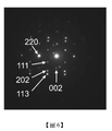
兩透明導電膜包含具有金屬奈米線的交叉部之奈米構造網絡與黏結劑樹脂。較佳為藉由金屬奈米線的交叉部之至少一部分經熔接的奈米構造網絡而構成。作為構成上述網絡之手段,可舉出將金屬奈米線的分散液(金屬奈米線油墨)塗佈於基材上後進行乾燥,較佳可舉出進行加熱或光照射等之處理,使金屬奈米線的交叉部之至少一部分熔接者。金屬奈米線的交叉部熔接者,係可由穿透型電子顯微鏡(TEM)的電子線繞射圖型之解析來確認。具體而言,可解析金屬奈米線彼此交叉的地方之電子線繞射圖型,由結晶構造變化(再結晶之發生)來確認。The two transparent conductive films include a nanostructured network with intersections of metal nanowires and a binder resin. Preferably, it is composed of a nanostructure network that is welded to at least a part of the intersections of the metal nanowires. As means for forming the above-mentioned network, it is possible to apply a dispersion liquid of metal nanowires (metal nanowire ink) on the substrate and then dry it. At least a part of the intersections of the metal nanowires is welded. Welding of the intersections of metal nanowires can be confirmed by analyzing electron beam diffraction patterns with a transmission electron microscope (TEM). Specifically, it is possible to analyze the electron beam diffraction pattern at the place where metal nanowires intersect each other, and confirm it by changing the crystal structure (occurrence of recrystallization).
作為金屬奈米線之製造方法,可使用眾所周知的製造方法。例如,銀奈米線可使用多元醇(Poly-ol)法,藉由在聚乙烯吡咯啶酮存在下將硝酸銀還原而合成(參照Chem. Mater., 2002, 14, 4736)。金奈米線亦同樣,可藉由在聚乙烯基吡咯啶酮存在下將氯金酸水合物還原而合成(參照J. Am. Chem. Soc., 2007, 129, 1733)。關於銀奈米線及金奈米線的大規模的合成及精製技術,在國際公開第2008/073143號小冊與國際公開第2008/046058號小冊中有詳細記述。具有多孔構造的金奈米管係可藉由將銀奈米線當作鑄模,將氯金酸溶液還原而合成。用於鑄模之銀奈米線係藉由與氯金酸之氧化還原反應而在溶液中溶出,結果可形成具有多孔構造的金奈米管(參照J. Am. Chem. Soc., 2004, 126, 3892-3901)。As a method for producing metal nanowires, well-known production methods can be used. For example, silver nanowires can be synthesized by reducing silver nitrate in the presence of polyvinylpyrrolidone using the poly-ol method (see Chem. Mater., 2002, 14, 4736). Gold nanowires can also be synthesized by reducing chloroauric acid hydrate in the presence of polyvinylpyrrolidone (refer to J. Am. Chem. Soc., 2007, 129, 1733). The techniques for large-scale synthesis and purification of silver nanowires and gold nanowires are described in detail in International Publication No. 2008/073143 and International Publication No. 2008/046058. Gold nanotubes with a porous structure can be synthesized by reducing the chloroauric acid solution using silver nanowires as a mold. The silver nanowires used in the mold are dissolved in the solution by the redox reaction with chloroauric acid, resulting in the formation of gold nanotubes with a porous structure (refer to J. Am. Chem. Soc., 2004, 126 , 3892-3901).
金屬奈米線之直徑的粗細之平均較佳為1~500nm,更佳為5~200nm,尤佳為5~100nm,特佳為10~50nm。金屬奈米線之長軸的長度之平均較佳為1~100μm,更佳為1~80μm,尤佳為2~70μm,特佳為5~50μm。金屬奈米線係直徑的粗細之平均及長軸的長度之平均較佳為滿足上述範圍,同時縱橫比之平均大於5,更佳為10以上,尤佳為100以上,特佳為200以上。此處,縱橫比係將金屬奈米線之平均直徑近似b,將長軸之平均長度近似a時,以a/b所求出的值。a及b係使用掃描型電子顯微鏡(SEM)及光學顯微鏡進行測定。具體而言,b(平均直徑)係使用電場發射型掃描電子顯微鏡JSM-7000F(日本電子股份有限公司製),測定經任意選擇的100條銀奈米線之尺寸(長度),作為所得之測定值的算術平均值而決定。又,於a(平均長度)之算出中,使用形狀測定雷射顯微鏡VK-X200(KEYENCE股份有限公司製),測定經任意選擇的100條銀奈米線之尺寸(長度),作為所得之測定值的算術平均值而決定。The average thickness of the diameter of the metal nanowires is preferably 1-500 nm, more preferably 5-200 nm, especially preferably 5-100 nm, particularly preferably 10-50 nm. The average length of the major axis of the metal nanowires is preferably 1-100 μm, more preferably 1-80 μm, particularly preferably 2-70 μm, and particularly preferably 5-50 μm. The average thickness of the metal nanowire diameter and the average length of the long axis preferably satisfy the above range, and the average aspect ratio is greater than 5, more preferably 10 or greater, especially preferably 100 or greater, and most preferably 200 or greater. Here, the aspect ratio is a value obtained by a/b when the average diameter of the metal nanowires is approximated to b and the average length of the long axis is approximated to a. a and b are measured using a scanning electron microscope (SEM) and an optical microscope. Specifically, b (average diameter) is measured using an electric field emission scanning electron microscope JSM-7000F (manufactured by JEOL Ltd.) to measure the size (length) of 100 arbitrarily selected silver nanowires, and it is obtained as a measurement determined by the arithmetic mean of the values. In addition, in the calculation of a (average length), the size (length) of 100 arbitrarily selected silver nanowires was measured using a shape measuring laser microscope VK-X200 (manufactured by KEYENCE Co., Ltd.), and it was obtained as the measurement determined by the arithmetic mean of the values.
作為金屬奈米線之材料,例如可舉出選自由金、銀、鉑、銅、鎳、鐵、鈷、鋅、釕、銠、鈀、鎘、鋨、銥所成之群組中的至少1種及組合此等金屬之合金等。為了得到具有低的片電阻且高的全光線透過率之塗膜,較佳為包含至少1種的金、銀及銅之任一者。此等金屬由於導電性高,故於得到一定的片電阻時,可減少金屬佔面之密度,因此可實現高的全光線穿透率。於此等金屬之中,更佳為包含金或銀的至少1種。最佳為銀奈米線。As the material of metal nanowires, for example, at least one material selected from the group consisting of gold, silver, platinum, copper, nickel, iron, cobalt, zinc, ruthenium, rhodium, palladium, cadmium, osmium, and iridium can be mentioned. Alloys of species and combinations of these metals, etc. In order to obtain a coating film having a low sheet resistance and a high total light transmittance, it is preferable to contain at least one of gold, silver, and copper. Due to the high conductivity of these metals, when a certain sheet resistance is obtained, the density of the metal area can be reduced, so a high total light transmittance can be achieved. Among these metals, at least one of gold and silver is more preferably contained. The best is silver nanowires.
作為黏結劑樹脂,只要是具有透明性者,則可無限制地應用,但使用利用多元醇法的金屬奈米線時,從與其製造用溶劑(多元醇)的相溶性之觀點來看,較佳為使用可溶於醇、水或醇與水的混合溶劑之黏結劑樹脂。例如,可舉出聚-N-乙烯基吡咯啶酮、甲基纖維素、羥乙基纖維素、羧甲基纖維素等之親水性纖維素系樹脂、丁醛樹脂、聚-N-乙烯基乙醯胺(PNVA(註冊商標))。聚-N-乙烯基乙醯胺為N-乙烯基乙醯胺(NVA)的均聚物。作為N-乙烯基乙醯胺共聚物,亦可使用含有70莫耳%以上的N-乙烯基乙醯胺(NVA)作為單體單元之共聚物。作為能與NVA共聚合的單體,例如可舉出N-乙烯基甲醯胺、N-乙烯基吡咯啶酮、丙烯酸、甲基丙烯酸、丙烯酸鈉、甲基丙烯酸鈉、丙烯醯胺、丙烯腈。若共聚合成分之含量變多,則所得之透明導電膜的片電阻變高,有與金屬奈米線的混合性或與基板的密著性降低之傾向,另外有耐熱性(熱分解開始溫度)亦降低之傾向,因此,來自N-乙烯基乙醯胺的單體單元在聚合物中較佳為含有70莫耳%以上,更佳為含有80莫耳%以上,尤佳為含有90莫耳%以上。如此的聚合物係絕對分子量所得之重量平均分子量較佳為3萬~400萬,更佳為10萬~300萬,尤佳為30萬~150萬。黏結劑樹脂為水溶性時,絕對分子量係藉由以下方法進行測定。As the binder resin, as long as it is transparent, it can be used without limitation. However, when using metal nanowires by the polyol method, it is less suitable from the viewpoint of compatibility with the solvent (polyol) for production. It is preferable to use a binder resin soluble in alcohol, water or a mixed solvent of alcohol and water. For example, hydrophilic cellulose-based resins such as poly-N-vinylpyrrolidone, methylcellulose, hydroxyethylcellulose, carboxymethylcellulose, butyral resin, poly-N-vinyl Acetamide (PNVA (registered trademark)). Poly-N-vinylacetamide is a homopolymer of N-vinylacetamide (NVA). As the N-vinylacetamide copolymer, a copolymer containing 70 mol% or more of N-vinylacetamide (NVA) as a monomer unit can also be used. Examples of monomers that can be copolymerized with NVA include N-vinylformamide, N-vinylpyrrolidone, acrylic acid, methacrylic acid, sodium acrylate, sodium methacrylate, acrylamide, and acrylonitrile . When the content of the copolymerization component increases, the sheet resistance of the obtained transparent conductive film increases, and the mixing property with the metal nanowires or the adhesion with the substrate tends to decrease. In addition, it has heat resistance (thermal decomposition initiation temperature ) also tends to decrease. Therefore, the monomer unit from N-vinyl acetamide preferably contains more than 70 mole % in the polymer, more preferably contains more than 80 mole %, and is especially preferably contains 90 mole % ear% or more. Such a polymer has a weight average molecular weight obtained by absolute molecular weight, preferably from 30,000 to 4 million, more preferably from 100,000 to 3 million, and most preferably from 300,000 to 1.5 million. When the binder resin is water-soluble, the absolute molecular weight is measured by the following method.
<絕對分子量測定> 使黏結劑樹脂溶解於下述洗提液中,靜置20小時。此溶液中的黏結劑樹脂之濃度為0.05質量%。 <Absolute Molecular Weight Measurement> The binder resin was dissolved in the following eluent, and allowed to stand for 20 hours. The concentration of the binder resin in this solution was 0.05% by mass.
以0.45μm薄膜過濾器過濾該溶液,以GPC-MALS分析濾液,算出絕對分子量基準的重量平均分子量。 GPC:昭和電工股份有限公司製Shodex(註冊商標) SYSTEM21 管柱:東曹股份有限公司製TSKgel(註冊商標)G6000PW 管柱溫度:40℃ 洗提液:0.1mol/L NaH 2PO 4水溶液+0.1mol/L Na 2HPO 4水溶液 流速:0.64mL/min 試料注入量:100μL MALS檢測器:Wyatt Technology Corporation,DAWN (註冊商標)DSP 雷射波長:633nm 多角度擬合法:Berry法 This solution was filtered through a 0.45 μm membrane filter, and the filtrate was analyzed by GPC-MALS to calculate the weight average molecular weight based on the absolute molecular weight. GPC: Shodex (registered trademark) SYSTEM21 manufactured by Showa Denko Co., Ltd. Column: TSKgel (registered trademark) G6000PW manufactured by Tosoh Co., Ltd. Column temperature: 40°C Eluent: 0.1 mol/L NaH 2 PO 4 aqueous solution + 0.1 mol/L Na 2 HPO 4 aqueous solution flow rate: 0.64mL/min sample injection volume: 100μL MALS detector: Wyatt Technology Corporation, DAWN (registered trademark) DSP laser wavelength: 633nm multi-angle fitting method: Berry method
上述樹脂可單獨使用,也可組合2種以上而使用。組合2種以上時,可為單純的混合,也可使用共聚物。These resins may be used alone or in combination of two or more. When combining 2 or more types, simple mixing may be sufficient, and a copolymer may also be used.
第一及第二透明導電膜係如前述各自包含具有金屬奈米線的交叉部之奈米構造網絡與黏結劑樹脂。第一及第二透明導電膜係可藉由將包含使金屬奈米線均勻地分散且溶解黏結劑樹脂的溶劑之金屬奈米線油墨,在透明樹脂薄膜之兩主面上分別地印刷等而塗佈,乾燥去除溶劑而形成。The first and second transparent conductive films each include a nanostructured network with intersections of metal nanowires and a binder resin as described above. The first and second transparent conductive films can be formed by printing metal nanowire ink containing a solvent that uniformly disperses the metal nanowires and dissolves the binder resin on both main surfaces of the transparent resin film, etc. Formed by coating, drying to remove solvent.
溶劑只要是金屬奈米線良好地分散,且溶解黏結劑樹脂但不溶解透明樹脂薄膜之溶劑,則沒有特別的限定。使用以多元醇法所合成的金屬奈米線時,從與其製造用溶劑(多元醇)的相溶性之觀點來看,較佳為使用醇、水或醇與水的混合溶劑。如前述,黏結劑樹脂亦較佳為使用可溶於醇、水或醇與水的混合溶劑中的黏結劑樹脂。從容易控制黏結劑樹脂的乾燥速度來看,較佳為使用醇與水的混合溶劑。醇較佳為包含至少1種的以C nH 2n+1OH(n為1~3之整數)表示的碳原子數為1~3的飽和一元醇(甲醇、乙醇、正丙醇及異丙醇)[以下僅記載為「碳原子數為1~3的飽和一元醇」]。更佳為在全部醇中包含40質量%以上的碳原子數為1~3的飽和一元醇。若使用碳原子數為1~3的飽和一元醇,則溶劑的乾燥變容易,因此製程上有利。作為醇,可併用碳原子數為1~3的飽和一元醇以外之醇。作為可併用的碳原子數為1~3的飽和一元醇以外之醇,例如可舉出乙二醇、丙二醇、乙二醇單甲基醚、乙二醇單乙基醚、丙二醇單甲基醚、丙二醇單乙基醚。藉由併用此等醇與碳原子數為1~3的飽和一元醇,可調整溶劑的乾燥速度。混合溶劑中的全部醇之含有率宜為5~90質量%。混合溶劑中的醇之含有率未達5質量%或超過90質量%時,有在塗佈時發生條紋(塗佈斑)之情況。 The solvent is not particularly limited as long as the metal nanowires are well dispersed and the binder resin is dissolved but the transparent resin film is not dissolved. When using the metal nanowires synthesized by the polyol method, it is preferable to use alcohol, water, or a mixed solvent of alcohol and water from the viewpoint of compatibility with the solvent (polyol) for production. As mentioned above, it is also preferable to use a binder resin that is soluble in alcohol, water, or a mixed solvent of alcohol and water. From the viewpoint of easy control of the drying rate of the binder resin, it is preferable to use a mixed solvent of alcohol and water. The alcohol is preferably a saturated monohydric alcohol (methanol, ethanol, n-propanol and isopropanol) with 1 to 3 carbon atoms represented by C n H 2n+1 OH (n is an integer of 1 to 3) containing at least one Alcohol) [hereinafter only described as "a saturated monohydric alcohol having 1 to 3 carbon atoms"]. More preferably, 40% by mass or more of saturated monohydric alcohols having 1 to 3 carbon atoms is included in all alcohols. When a saturated monohydric alcohol having 1 to 3 carbon atoms is used, the drying of the solvent becomes easy, which is advantageous in terms of manufacturing process. Alcohols other than saturated monohydric alcohols having 1 to 3 carbon atoms may be used in combination. Examples of alcohols other than saturated monohydric alcohols having 1 to 3 carbon atoms that can be used in combination include ethylene glycol, propylene glycol, ethylene glycol monomethyl ether, ethylene glycol monoethyl ether, and propylene glycol monomethyl ether. , Propylene glycol monoethyl ether. By using these alcohols in combination with a saturated monohydric alcohol having 1 to 3 carbon atoms, the drying rate of the solvent can be adjusted. The content of all the alcohols in the mixed solvent is preferably 5 to 90% by mass. When the alcohol content in the mixed solvent is less than 5% by mass or exceeds 90% by mass, streaks (coating unevenness) may occur during coating.
金屬奈米線油墨可藉由將黏結劑樹脂、金屬奈米線及溶劑以自轉公轉攪拌機等攪拌、混合而製造。金屬奈米線油墨中含有的黏結劑樹脂之含量較佳為0.01~1.0質量%之範圍。金屬奈米線油墨中含有的金屬奈米線之含量較佳為0.01~1.0質量%之範圍。金屬奈米線油墨中含有的溶劑之含量較佳為98.0~99.98質量%之範圍。The metal nanowire ink can be produced by stirring and mixing a binder resin, metal nanowires, and a solvent with a self-rotating mixer or the like. The content of the binder resin contained in the metal nanowire ink is preferably in the range of 0.01 to 1.0% by mass. The content of the metal nanowires contained in the metal nanowire ink is preferably in the range of 0.01 to 1.0% by mass. The content of the solvent contained in the metal nanowire ink is preferably in the range of 98.0 to 99.98% by mass.
金屬奈米線油墨之印刷可藉由棒塗法、旋轉塗佈法、噴塗法、凹版法、狹縫塗佈法等之印刷法進行。藉由印刷所形成的印刷膜或圖型之形狀係沒有特別的限定,但可舉出形成在基材上的配線、電極的圖型之形狀、或被覆基材的全面或一部分之面的膜(實心圖型)之形狀等。所形成的印刷膜係藉由使溶劑乾燥而具有導電性。透明導電膜的乾燥厚度,雖然隨著所使用的金屬奈米線之直徑、所欲的片電阻值等而不同,但較佳為10~300nm,更佳為30~200nm。若透明導電膜的乾燥厚度為10nm以上,則金屬奈米線的交點之數增加,因此可得到良好的導電性。又,若透明導電膜的乾燥厚度為300nm以下,則光變容易透過,可抑制金屬奈米線所造成的反射,因此可得到良好的光學特性。視需要亦可對於透明導電膜進行適宜的光照射。The printing of metal nanowire ink can be carried out by printing methods such as bar coating method, spin coating method, spray coating method, gravure method, and slit coating method. The shape of the printed film or pattern formed by printing is not particularly limited, but examples include wiring formed on the substrate, the shape of the electrode pattern, or a film covering the entire or part of the substrate ( solid graphics) shape, etc. The formed printed film is made conductive by drying the solvent. The dry thickness of the transparent conductive film is preferably 10-300nm, more preferably 30-200nm, although it varies with the diameter of the metal nanowires used, the desired sheet resistance value, and the like. If the dry thickness of the transparent conductive film is more than 10 nm, the number of intersection points of the metal nanowires increases, so good conductivity can be obtained. In addition, if the dry thickness of the transparent conductive film is 300 nm or less, light can easily pass through, and reflection caused by metal nanowires can be suppressed, so that good optical characteristics can be obtained. Appropriate light irradiation can also be performed with respect to a transparent conductive film as needed.
<保護膜> 本實施形態之透明導電膜係分別在第一透明導電膜上具有第一保護膜,在第二透明導電膜上具有第二保護膜。 <Protective film> The transparent conductive film of this embodiment has a first protective film on the first transparent conductive film, and a second protective film on the second transparent conductive film.
保護透明導電圖型膜的保護膜為硬化性樹脂組成物的熱硬化膜。作為硬化性樹脂組成物,較佳為包含(A)含有羧基的聚胺基甲酸酯、(B)在分子內具有二個以上環氧基的環氧化合物與(C)硬化促進劑者。藉由將硬化性樹脂組成物,在上述第一、第二透明導電膜上印刷、塗佈等而形成,使其硬化而形成保護膜。硬化性樹脂組成物之硬化,例如當使用熱硬化性樹脂組成物時,可藉由加熱・乾燥它,使其熱硬化而進行。尚且,以後,為了表述的簡單化,將「(B)在分子內具有二個以上環氧基的環氧化合物」僅記載為「(B)環氧化合物」。The protective film for protecting the transparent conductive pattern film is a thermosetting film of a curable resin composition. The curable resin composition is preferably one containing (A) carboxyl group-containing polyurethane, (B) an epoxy compound having two or more epoxy groups in the molecule, and (C) a curing accelerator. The curable resin composition is formed by printing, coating, etc. on the first and second transparent conductive films, and cured to form a protective film. Curing of the curable resin composition, for example, when using a thermosetting resin composition, can be carried out by heating and drying it to make it thermally harden. In addition, hereinafter, "(B) an epoxy compound having two or more epoxy groups in the molecule" will be simply described as "(B) epoxy compound" for the sake of simplification of expression.
(A)含有羧基的聚胺基甲酸酯 (A)含有羧基的聚胺基甲酸酯係其重量平均分子量較佳為1,000~100,000,更佳為2,000~70,000,尤佳為3,000~50,000。本說明書中,含有羧基的聚胺基甲酸酯之重量平均分子量係以GPC所測定的聚苯乙烯換算之值。若含有羧基的聚胺基甲酸酯之重量平均分子量為1,000以上,則充分發揮印刷後的塗膜之延伸度、可撓性及強度。若含有羧基的聚胺基甲酸酯之重量平均分子量為100,000以下,則在溶劑中的溶解性良好,且溶解後的聚胺基甲酸酯溶液之黏度亦不過高,處理性優異。 (A) Polyurethane containing carboxyl groups (A) The carboxyl group-containing polyurethane has a weight average molecular weight of preferably 1,000-100,000, more preferably 2,000-70,000, and especially preferably 3,000-50,000. In this specification, the weight average molecular weight of the carboxyl group-containing polyurethane is a value in terms of polystyrene measured by GPC. When the weight average molecular weight of the carboxyl group-containing polyurethane is 1,000 or more, the elongation, flexibility, and strength of the coated film after printing can be fully exhibited. When the carboxyl group-containing polyurethane has a weight-average molecular weight of 100,000 or less, the solubility in a solvent is good, and the viscosity of the polyurethane solution after dissolution is not too high, so the handleability is excellent.
本說明書中,只要沒有特別預先指明,則含有羧基的聚胺基甲酸酯之GPC測定條件為如以下。 裝置名:日本分光股份有限公司製HPLC單元HSS-2000 管柱:Shodex管柱LF-804 移動相:四氫呋喃 流速:1.0mL/min 檢測器:日本分光股份有限公司製RI-2031Plus 溫度:40.0℃ 試料量:樣品環100μL 試料濃度:調製成約0.1質量% In this specification, unless otherwise specified, the GPC measurement conditions of the carboxyl group-containing polyurethane are as follows. Device name: HPLC unit HSS-2000 manufactured by JASCO Co., Ltd. Column: Shodex column LF-804 Mobile Phase: Tetrahydrofuran Flow rate: 1.0mL/min Detector: RI-2031Plus manufactured by JASCO Co., Ltd. Temperature: 40.0°C Sample volume: sample loop 100μL Sample concentration: adjusted to about 0.1% by mass
(A)含有羧基的聚胺基甲酸酯之酸價較佳為10~140mg-KOH/g,更佳為15~130mg-KOH/g。若含有羧基的聚胺基甲酸酯之酸價為10mg-KOH/g以上,則保護膜的耐溶劑性良好,樹脂組成物的硬化性亦良好。若含有羧基的聚胺基甲酸酯之酸價為140mg-KOH/g以下,則聚胺基甲酸酯在溶劑中的溶解性良好,容易將樹脂組成物的黏度調整至所欲的黏度。又,不易引起硬化物過硬所造成的基材薄膜之翹曲等之問題。(A) The acid value of the carboxyl group-containing polyurethane is preferably 10-140 mg-KOH/g, more preferably 15-130 mg-KOH/g. When the acid value of the carboxyl group-containing polyurethane is 10 mg-KOH/g or more, the solvent resistance of the protective film is good, and the curability of the resin composition is also good. When the acid value of the carboxyl group-containing polyurethane is 140 mg-KOH/g or less, the solubility of the polyurethane in a solvent is good, and it is easy to adjust the viscosity of the resin composition to a desired viscosity. Also, it is less likely to cause problems such as warping of the base film due to too hard a cured product.
本說明書中,含有羧基的聚胺基甲酸酯之酸價係藉由以下方法所測定之值。 於100mL三角燒瓶中,以精密天平精秤試料約0.2g,於其中加入乙醇/甲苯=1/2(質量比)的混合溶劑10ml進行溶解。再者,於該容器中添加1~3滴的酚酞乙醇溶液作為指示劑,充分地攪拌直到試料成為均勻為止。以0.1N氫氧化鉀-乙醇溶液滴定它,將指示劑之微紅色持續30秒鐘時當作中和的終點。將用下述計算式所得之值當作含有羧基的聚胺基甲酸酯之酸價。 酸價(mg-KOH/g)=[B×f×5.611]/S B:0.1N氫氧化鉀-乙醇溶液之使用量(ml) f:0.1N氫氧化鉀-乙醇溶液之因數(factor) S:試料的採集量(g) In this specification, the acid value of the carboxyl group-containing polyurethane is a value measured by the following method. In a 100mL Erlenmeyer flask, about 0.2g of the sample was accurately weighed with a precision balance, and 10ml of a mixed solvent of ethanol/toluene=1/2 (mass ratio) was added therein for dissolution. Furthermore, 1 to 3 drops of phenolphthalein ethanol solution was added to the container as an indicator, and the mixture was stirred sufficiently until the sample became uniform. Titrate it with 0.1N potassium hydroxide-ethanol solution, and the reddish color of the indicator lasts for 30 seconds as the end point of neutralization. The value obtained by the following calculation formula was regarded as the acid value of the carboxyl group-containing polyurethane. Acid value (mg-KOH/g)=[B×f×5.611]/S B: Amount of 0.1N potassium hydroxide-ethanol solution (ml) f: factor of 0.1N potassium hydroxide-ethanol solution (factor) S: Sample collection amount (g)
(A)含有羧基的聚胺基甲酸酯係更具體而言,為將(a1)聚異氰酸酯化合物、(a2)多元醇化合物及(a3)具有羧基的二羥基化合物使用作為單體而合成之聚胺基甲酸酯。於耐候性及耐光性之觀點中,(a1)、(a2)、(a3)宜各自不包含具有芳香族化合物等之共軛性的官能基為佳。以下,詳細地說明各單體。(A) Carboxyl group-containing polyurethane is more specifically synthesized using (a1) polyisocyanate compound, (a2) polyol compound, and (a3) carboxyl group-containing dihydroxy compound as monomers. Polyurethane. From the viewpoint of weather resistance and light resistance, each of (a1), (a2), and (a3) preferably does not contain a conjugated functional group such as an aromatic compound. Hereinafter, each monomer will be described in detail.
(a1)聚異氰酸酯化合物 作為(a1)聚異氰酸酯化合物,通常使用每1分子的異氰酸酯基為2個的二異氰酸酯。作為聚異氰酸酯化合物,例如可舉出脂肪族聚異氰酸酯、脂環式聚異氰酸酯等,可單獨或組合2種以上而使用該等。於含有羧基的聚胺基甲酸酯不進行凝膠化之範圍內,亦可少量使用具有3個以上異氰酸酯基的聚異氰酸酯。 (a1) polyisocyanate compound As (a1) polyisocyanate compound, the diisocyanate which has 2 isocyanate groups per 1 molecule is used normally. As a polyisocyanate compound, aliphatic polyisocyanate, an alicyclic polyisocyanate, etc. are mentioned, for example, These can be used individually or in combination of 2 or more types. A small amount of polyisocyanate having three or more isocyanate groups can also be used as long as the carboxyl group-containing polyurethane does not undergo gelation.
作為脂肪族聚異氰酸酯,例如可舉出1,3-三亞甲基二異氰酸酯、1,4-四亞甲基二異氰酸酯、1,6-六亞甲基二異氰酸酯、1,9-九亞甲基二異氰酸酯、1,10-十亞甲基二異氰酸酯、2,2,4-三甲基六亞甲基二異氰酸酯、2,4,4-三甲基六亞甲基二異氰酸酯、離胺酸二異氰酸酯、2,2’-二乙基醚二異氰酸酯、二聚酸二異氰酸酯等。Examples of aliphatic polyisocyanate include 1,3-trimethylene diisocyanate, 1,4-tetramethylene diisocyanate, 1,6-hexamethylene diisocyanate, 1,9-nonamethylene diisocyanate, Diisocyanate, 1,10-decamethylene diisocyanate, 2,2,4-trimethylhexamethylene diisocyanate, 2,4,4-trimethylhexamethylene diisocyanate, lysine diisocyanate Isocyanate, 2,2'-diethyl ether diisocyanate, dimer acid diisocyanate, etc.
作為脂環式聚異氰酸酯,例如可舉出1,4-環己烷二異氰酸酯、1,3-雙(異氰酸基甲基)環己烷、1,4-雙(異氰酸基甲基)環己烷、3-異氰酸基甲基-3,5,5-三甲基環己基異氰酸酯(IPDI,異佛爾酮二異氰酸酯)、雙-(4-異氰酸基環己基)甲烷(氫化MDI)、氫化(1,3-或1,4-)苯二甲基二異氰酸酯、降莰烷二異氰酸酯等。Examples of alicyclic polyisocyanates include 1,4-cyclohexane diisocyanate, 1,3-bis(isocyanatomethyl)cyclohexane, 1,4-bis(isocyanatomethyl) ) cyclohexane, 3-isocyanatomethyl-3,5,5-trimethylcyclohexyl isocyanate (IPDI, isophorone diisocyanate), bis-(4-isocyanatocyclohexyl)methane (hydrogenated MDI), hydrogenated (1,3- or 1,4-) xylylene diisocyanate, norbornane diisocyanate, etc.
作為(a1)聚異氰酸酯化合物,藉由使用異氰酸酯基(-NCO基)中的碳原子以外之碳原子之數為6~30的脂環式化合物,可得到高溫高濕時之可靠性高,適合電子機器零件的構件之保護膜。於上述例示的脂環式聚異氰酸酯之中,較佳為1,4-環己烷二異氰酸酯、異佛爾酮二異氰酸酯、雙-(4-異氰酸基環己基)甲烷、1,3-雙(異氰酸基甲基)環己烷、1,4-雙(異氰酸基甲基)環己烷。As the (a1) polyisocyanate compound, by using an alicyclic compound having 6 to 30 carbon atoms other than the carbon atoms in the isocyanate group (-NCO group), high reliability at high temperature and high humidity can be obtained, and it is suitable Protective film for components of electronic machine parts. Among the alicyclic polyisocyanates exemplified above, 1,4-cyclohexane diisocyanate, isophorone diisocyanate, bis-(4-isocyanatocyclohexyl)methane, 1,3- Bis(isocyanatomethyl)cyclohexane, 1,4-bis(isocyanatomethyl)cyclohexane.
如上述於耐候性及耐光性之觀點中,作為(a1)聚異氰酸酯化合物,較佳為使用不具有芳香環的化合物者。因此,視需要使用芳香族聚異氰酸酯、芳香脂肪族聚異氰酸酯時,此等之含量係相對於(a1)聚異氰酸酯化合物之總量(100mol%),較佳為50mol%以下,更佳為30mol%以下,尤佳為10mol%以下。It is preferable to use a compound which does not have an aromatic ring as (a1) polyisocyanate compound from a viewpoint of weather resistance and light resistance as mentioned above. Therefore, when aromatic polyisocyanate and araliphatic polyisocyanate are used as needed, their content is preferably 50 mol% or less, more preferably 30 mol% relative to the total amount (100 mol%) of the polyisocyanate compound (a1). Below, especially preferably below 10 mol%.
(a2)多元醇化合物 (a2)多元醇化合物(惟(a2)多元醇化合物中,不包含後述(a3)具有羧基的二羥基化合物)之數量平均分子量通常為250~50,000,較佳為400~10,000,更佳為500~5,000。多元醇化合物之數量平均分子量係在前述的條件下藉由GPC所測定的聚苯乙烯換算之值。 (a2) Polyol compound The number average molecular weight of (a2) polyol compound (except (a2) polyol compound does not include dihydroxy compound having carboxyl group in (a3) described later) is usually 250-50,000, preferably 400-10,000, more preferably 500 ~5,000. The number average molecular weight of the polyol compound is a value in terms of polystyrene measured by GPC under the aforementioned conditions.
(a2)多元醇化合物例如為聚碳酸酯多元醇、聚醚多元醇、聚酯多元醇、聚內酯多元醇、兩末端羥基化聚矽氧及源自以植物系油脂作為原料的C18(碳原子數18)不飽和脂肪酸及其聚合物之多元羧酸進行氫化,將羧酸轉換成羥基之碳原子數為18~72的多元醇化合物。於此等之中,從作為保護膜之耐水性、絕緣可靠性及與基材的密著性之平衡的觀點來看,(a2)多元醇化合物較佳為聚碳酸酯多元醇。(a2) Polyol compounds are, for example, polycarbonate polyols, polyether polyols, polyester polyols, polylactone polyols, hydroxylated polysiloxanes at both ends, and C18 (carbon Hydrogenation of polycarboxylic acid of unsaturated fatty acid and its polymer with 18 atoms, converting carboxylic acid into polyol compound with 18-72 carbon atoms of hydroxyl group. Among them, the (a2) polyol compound is preferably a polycarbonate polyol from the viewpoint of a balance between water resistance as a protective film, insulation reliability, and adhesion to a base material.
聚碳酸酯多元醇係可以碳原子數3~18之二醇作為原料,藉由與碳酸酯或光氣反應而得,例如以下的結構式(1)所示。

式(1)中,R 3係從對應的二醇(HO-R 3-OH)去除羥基後的殘基,為碳原子數3~18的伸烷基,n 3為正整數,較佳為2~50。 In formula (1), R 3 is the residue after removing the hydroxyl group from the corresponding diol (HO-R 3 -OH), and is an alkylene group with 3 to 18 carbon atoms, and n 3 is a positive integer, preferably 2~50.
式(1)所示的聚碳酸酯多元醇,具體而言,可藉由使用1,3-丙二醇、1,4-丁二醇、1,5-戊二醇、1,6-己二醇、3-甲基-1,5-戊二醇、1,8-辛二醇、1,3-環己烷二甲醇、1,4-環己烷二甲醇、1,9-壬二醇、2-甲基-1,8-辛二醇、1,10-癸二醇或1,2-十四烷二醇等作為原料而製造。The polycarbonate polyol represented by formula (1), specifically, can be obtained by using 1,3-propanediol, 1,4-butanediol, 1,5-pentanediol, 1,6-hexanediol , 3-methyl-1,5-pentanediol, 1,8-octanediol, 1,3-cyclohexanedimethanol, 1,4-cyclohexanedimethanol, 1,9-nonanediol, 2-Methyl-1,8-octanediol, 1,10-decanediol, 1,2-tetradecanediol, etc. are used as raw materials for production.
聚碳酸酯多元醇可為在其骨架中具有複數種的烷二基之聚碳酸酯多元醇(共聚合聚碳酸酯多元醇)。共聚合聚碳酸酯多元醇之使用,從防止(A)含有羧基的聚胺基甲酸酯的結晶化之觀點來看,有利的情況多。又,若考慮在溶劑中的溶解性,則較佳為併用具有分支骨架,在分支鏈之末端具有羥基的聚碳酸酯多元醇。The polycarbonate polyol may be a polycarbonate polyol (copolymerized polycarbonate polyol) having plural kinds of alkanediyl groups in its skeleton. The use of copolymerized polycarbonate polyol is often advantageous from the viewpoint of preventing crystallization of (A) carboxyl group-containing polyurethane. In addition, in consideration of solubility in a solvent, it is preferable to use together a polycarbonate polyol having a branched skeleton and having a hydroxyl group at the end of the branched chain.
(a3)含有羧基的二羥基化合物 作為(a3)含有羧基的二羥基化合物,具有2個由羥基、碳數為1或2的羥烷基所選出的任一者之分子量為200以下的羧酸或胺基羧酸,係在能控制交聯點之方面較宜。作為(a3)含有羧基的二羥基化合物,例如可舉出2,2-二羥甲基丙酸、2,2-二羥甲基丁酸、N,N-雙羥基乙基甘胺酸、N,N-雙羥基乙基丙胺酸等,於此等之中,從在溶劑中的溶解性高來看,較佳為2,2-二羥甲基丙酸及2,2-二羥甲基丁酸。(a3)含有羧基的二羥基化合物可單獨或組合2種以上而使用。 (a3) Dihydroxy compound containing carboxyl group As (a3) a dihydroxy compound containing a carboxyl group, it has two carboxylic acids or aminocarboxylic acids with a molecular weight of 200 or less selected from a hydroxyl group and a hydroxyalkyl group having 1 or 2 carbon atoms. It is preferable to control the point of cross-linking. Examples of (a3) dihydroxy compounds containing carboxyl groups include 2,2-dimethylolpropionic acid, 2,2-dimethylolbutyric acid, N,N-bishydroxyethylglycine, N , N-bishydroxyethylalanine, etc. Among these, 2,2-dimethylolpropionic acid and 2,2-dimethylolpropionic acid are preferred in view of their high solubility in solvents. butyric acid. (a3) The dihydroxy compound containing a carboxyl group can be used individually or in combination of 2 or more types.
(A)含有羧基的聚胺基甲酸酯可僅由上述3成分((a1)、(a2)及(a3))來合成。尚且,亦可進一步使(a4)單羥基化合物及/或(a5)單異氰酸酯化合物進行反應而合成。從耐候性及耐光性之觀點來看,(a4)單羥基化合物及(a5)單異氰酸酯化合物較佳為在分子內不含芳香環或碳-碳雙鍵的化合物。(A) The carboxyl group-containing polyurethane can be synthesized only from the above three components ((a1), (a2), and (a3)). Furthermore, (a4) monohydroxyl compound and/or (a5) monoisocyanate compound can also be made to react and synthesize|combine. The (a4) monohydroxy compound and (a5) monoisocyanate compound are preferably compounds that do not contain an aromatic ring or a carbon-carbon double bond in the molecule from the viewpoint of weather resistance and light resistance.
上述(A)含有羧基的聚胺基甲酸酯可藉由在如二月桂酸二丁錫之眾所周知的胺基甲酸酯化觸媒之存在下或不存在下,使用適當的有機溶劑,使上述(a1)聚異氰酸酯化合物、(a2)多元醇化合物、(a3)具有羧基的二羥基化合物進行反應而合成。使(a1)聚異氰酸酯化合物、(a2)多元醇化合物及(a3)具有羧基的二羥基化合物在無觸媒下反應者,係沒有考慮最後混入錫等之必要而較宜。The above-mentioned (A) carboxyl group-containing polyurethane can be obtained by making the above-mentioned ( a1) polyisocyanate compound, (a2) polyol compound, and (a3) dihydroxy compound having carboxyl group are reacted and synthesized. It is preferable to react (a1) polyisocyanate compound, (a2) polyol compound, and (a3) carboxyl-containing dihydroxy compound without a catalyst, without considering the necessity of adding tin etc. at the end.
有機溶劑只要與異氰酸酯化合物的反應性低者,則沒有特別的限定。有機溶劑不包含胺等之鹼性官能基,且沸點為50℃以上,較佳為80℃以上,更佳為100℃以上的溶劑較宜。作為如此的溶劑,例如可舉出甲苯、二甲苯、乙苯、硝基苯、環己烷、異佛爾酮、二乙二醇二甲基醚、乙二醇二乙醚、乙二醇單甲基醚乙酸酯、丙二醇單甲基醚乙酸酯、丙二醇單乙醚乙酸酯、二丙二醇單甲基醚乙酸酯、二乙二醇單乙醚乙酸酯、甲氧基丙酸甲酯、甲氧基丙酸乙酯、乙氧基丙酸甲酯、乙氧基丙酸乙酯、乙酸乙酯、乙酸正丁酯、乙酸異戊酯、乳酸乙酯、丙酮、甲基乙基酮、環己酮、N,N-二甲基甲醯胺、N,N-二甲基乙醯胺、N-甲基吡咯啶酮、γ-丁內酯及二甲亞碸。The organic solvent is not particularly limited as long as it has low reactivity with isocyanate compounds. The organic solvent does not contain basic functional groups such as amines and has a boiling point above 50°C, preferably above 80°C, more preferably above 100°C. Examples of such solvents include toluene, xylene, ethylbenzene, nitrobenzene, cyclohexane, isophorone, diethylene glycol dimethyl ether, ethylene glycol diethyl ether, ethylene glycol monomethyl ether, and Base ether acetate, propylene glycol monomethyl ether acetate, propylene glycol monoethyl ether acetate, dipropylene glycol monomethyl ether acetate, diethylene glycol monoethyl ether acetate, methyl methoxypropionate, Ethyl Methoxypropionate, Methyl Ethoxypropionate, Ethyl Ethoxypropionate, Ethyl Acetate, n-Butyl Acetate, Isoamyl Acetate, Ethyl Lactate, Acetone, Methyl Ethyl Ketone, Cyclohexanone, N,N-dimethylformamide, N,N-dimethylacetamide, N-methylpyrrolidone, gamma-butyrolactone and dimethyloxide.
若考慮生成的聚胺基甲酸酯之溶解性低的有機溶劑不宜,及電子材料用途中將聚胺基甲酸酯作為保護膜用油墨的原料,則有機溶劑較佳為丙二醇單甲基醚乙酸酯、丙二醇單乙基醚乙酸酯、二丙二醇單甲基醚乙酸酯、二乙二醇單乙基醚乙酸酯、γ-丁內酯或彼等之組合。If it is considered that organic solvents with low solubility of the generated polyurethane are not suitable, and polyurethane is used as a raw material for protective film inks in electronic materials, the organic solvent is preferably propylene glycol monomethyl ether Acetate, propylene glycol monoethyl ether acetate, dipropylene glycol monomethyl ether acetate, diethylene glycol monoethyl ether acetate, γ-butyrolactone, or combinations thereof.
原料之投入順序係沒有特別的限制,但通常先將(a2)多元醇化合物及(a3)具有羧基的二羥基化合物投入反應容器,使其溶解或分散於溶劑後,在20~150℃,更佳在60~120℃下,邊滴液(a1)聚異氰酸酯化合物邊添加,然後在30~160℃,更佳在50~130℃下使該等反應。The input sequence of the raw materials is not particularly limited, but usually the (a2) polyol compound and (a3) the dihydroxy compound having a carboxyl group are first put into the reaction vessel, and after they are dissolved or dispersed in the solvent, the Preferably at 60 to 120°C, the polyisocyanate compound (a1) is added dropwise, and then these are reacted at 30 to 160°C, more preferably at 50 to 130°C.
原料投入之莫耳比係按照目的之聚胺基甲酸酯的分子量及酸價進行調節。The molar ratio of raw materials input is adjusted according to the molecular weight and acid value of the polyurethane of interest.
具體而言,(a1)聚異氰酸酯化合物的異氰酸酯基:((a2)多元醇化合物的羥基+(a3)具有羧基的二羥基化合物的羥基)之莫耳比較佳為0.5~1.5:1,更佳為0.8~1.2:1,更佳為0.95~1.05:1。Specifically, the molar ratio of (a1) isocyanate group of polyisocyanate compound: ((a2) hydroxyl group of polyol compound + (a3) hydroxyl group of dihydroxy compound having carboxyl group) is preferably 0.5-1.5:1, more preferably 0.8-1.2:1, more preferably 0.95-1.05:1.
(a2)多元醇化合物的羥基:(a3)具有羧基的二羥基化合物的羥基之莫耳比較佳為1:0.1~30,更佳為1:0.3~10。(a2) The hydroxyl group of the polyol compound: (a3) The molar ratio of the hydroxyl group of the dihydroxy compound having a carboxyl group is preferably 1:0.1-30, more preferably 1:0.3-10.
(B)環氧化合物 作為(B)環氧化合物,可舉出雙酚A型環氧化合物、氫化雙酚A型環氧樹脂、雙酚F型環氧樹脂、酚醛清漆型環氧樹脂、苯酚酚醛清漆型環氧樹脂、甲酚酚醛清漆環氧樹脂、N-環氧丙基型環氧樹脂、雙酚A的酚醛清漆型環氧樹脂、螯合物型環氧樹脂、乙二醛型環氧樹脂、含胺基的環氧樹脂、橡膠改質環氧樹脂、二環戊二烯酚醛型環氧樹脂、聚矽氧改質環氧樹脂、ε-己內酯改質環氧樹脂、含有環氧丙基的脂肪族型環氧樹脂、含有環氧丙基的脂環式環氧樹脂等之在一分子中具有2個以上環氧基的環氧化合物。 (B) epoxy compound Examples of (B) epoxy compounds include bisphenol A epoxy compounds, hydrogenated bisphenol A epoxy resins, bisphenol F epoxy resins, novolac epoxy resins, and phenol novolac epoxy resins. , cresol novolac epoxy resin, N-glycidyl type epoxy resin, bisphenol A novolak type epoxy resin, chelate type epoxy resin, glyoxal type epoxy resin, amino group-containing epoxy resin, rubber modified epoxy resin, dicyclopentadiene novolac epoxy resin, polysiloxane modified epoxy resin, ε-caprolactone modified epoxy resin, glycidyl-containing fat Epoxy compounds having two or more epoxy groups in one molecule, such as family-type epoxy resins and alicyclic epoxy resins containing glycidyl groups.
可更適宜地使用在一分子中具有3個以上環氧基的環氧化合物。作為如此的環氧化合物,例如可舉出EHPE(註冊商標)3150(股份有限公司DAICEL製)、jER604(三菱化學股份有限公司製)、EPICLON EXA-4700 (DIC股份有限公司製)、EPICLON HP-7200(DIC股份有限公司製)、季戊四醇四環氧丙基醚、季戊四醇三環氧丙基醚、TEPIC-S(日產化學股份有限公司製)等。An epoxy compound having three or more epoxy groups in one molecule can be more suitably used. Examples of such epoxy compounds include EHPE (registered trademark) 3150 (manufactured by DAICEL Co., Ltd.), jER604 (manufactured by Mitsubishi Chemical Corporation), EPICLON EXA-4700 (manufactured by DIC Co., Ltd.), EPICLON HP- 7200 (manufactured by DIC Co., Ltd.), pentaerythritol tetraglycidyl ether, pentaerythritol triglycidyl ether, TEPIC-S (manufactured by Nissan Chemical Co., Ltd.), and the like.
(B)環氧化合物可在分子內具有芳香環。當時,相對於上述(A)含有羧基的聚胺基甲酸酯與(B)環氧化合物之合計質量,(B)環氧化合物之質量較佳為20質量%以下。(B) An epoxy compound may have an aromatic ring in a molecule|numerator. In that case, it is preferable that the mass of (B) epoxy compound is 20 mass % or less with respect to the total mass of said (A) carboxyl group containing polyurethane and (B) epoxy compound.
(B)環氧化合物與(A)含有羧基的聚胺基甲酸酯之摻合比例,係相對於(B)環氧化合物的環氧基,聚胺基甲酸酯中的羧基之當量比較佳為0.5~1.5,更佳為0.7~1.3,尤佳為0.9~1.1。(B) The blending ratio of epoxy compound and (A) polyurethane containing carboxyl group is compared with the equivalent weight of carboxyl group in polyurethane relative to the epoxy group of (B) epoxy compound It is preferably 0.5 to 1.5, more preferably 0.7 to 1.3, and most preferably 0.9 to 1.1.
(C)硬化促進劑 作為(C)硬化促進劑,可舉出三苯基膦、三丁基膦等之膦系化合物(北興化學工業股份有限公司製)、Curezol (註冊商標)(咪唑系環氧樹脂硬化劑:四國化成工業股份有限公司製)、2-苯基-4-甲基-5-羥基甲基咪唑、U-CAT(註冊商標)SA系列(DBU鹽:San-Apro股份有限公司製)、Irgacure(註冊商標)184等。(C)硬化促進劑之使用量係若使用量太少,則無添加的效果,若使用量過多,則電絕緣性降低,故相對於(A)含有羧基的聚胺基甲酸酯與(B)環氧化合物之合計質量,較佳為0.1~10質量%,更佳為0.5~6質量%,尤佳為0.5~5質量%,特佳為0.5~3質量%。 (C) hardening accelerator Examples of the (C) hardening accelerator include phosphine-based compounds such as triphenylphosphine and tributylphosphine (manufactured by Beixing Chemical Industry Co., Ltd.), Curezol (registered trademark) (imidazole-based epoxy resin hardener: four National Chemical Industry Co., Ltd.), 2-phenyl-4-methyl-5-hydroxymethylimidazole, U-CAT (registered trademark) SA series (DBU salt: San-Apro Co., Ltd.), Irgacure ( Registered trademark) 184 et al. (C) If the amount of hardening accelerator used is too small, there will be no effect of addition. If the amount used is too large, the electrical insulation will be reduced. Therefore, compared with (A) carboxyl group-containing polyurethane and ( B) The total mass of epoxy compounds is preferably 0.1 to 10% by mass, more preferably 0.5 to 6% by mass, particularly preferably 0.5 to 5% by mass, particularly preferably 0.5 to 3% by mass.
亦可併用硬化助劑。作為硬化助劑,例如可舉出多官能硫醇化合物或氧環丁烷化合物等。作為多官能硫醇化合物,可舉出季戊四醇四(3-巰基丙酸酯)、參[(3-巰基丙醯氧基)-乙基]-異三聚氰酸酯、三羥甲基丙烷參(3-巰基丙酸酯)、Karenz(註冊商標)MT系列(昭和電工股份有限公司製)。作為氧環丁烷化合物,可舉出Aron Oxetane (註冊商標)系列(東亞合成股份有限公司製)、ETERNACOLL (註冊商標)OXBP或OXMA(宇部興產股份有限公司製)。硬化助劑之使用量係相對於(B)環氧化合物100質量份,較佳為0.1~10質量%,更佳為0.5~6質量%。若添加0.1質量份以上,則充分發揮助劑的效果,若為10質量份以下,則可以容易處理的速度進行硬化。A curing aid may also be used in combination. As a hardening aid, a polyfunctional thiol compound, an oxetane compound, etc. are mentioned, for example. Examples of polyfunctional thiol compounds include pentaerythritol tetrakis(3-mercaptopropionate), ginseng[(3-mercaptopropionyloxy)-ethyl]-isocyanurate, trimethylolpropane ginseng (3-mercaptopropionate), Karenz (registered trademark) MT series (manufactured by Showa Denko Co., Ltd.). Examples of the oxetane compound include Aron Oxetane (registered trademark) series (manufactured by Toagosei Co., Ltd.), ETERNACOLL (registered trademark) OXBP and OXMA (manufactured by Ube Industries, Ltd.). The usage-amount of a hardening aid is preferably 0.1-10 mass % with respect to 100 mass parts of (B) epoxy compounds, More preferably, it is 0.5-6 mass %. When adding 0.1 parts by mass or more, the effect of the auxiliary agent can be fully exhibited, and if it is not more than 10 parts by mass, hardening can be performed at a speed that is easy to handle.
(D)溶劑 於硬化性樹脂組成物中,較佳為含有95.0質量%以上99.9質量%以下的(D)溶劑,更佳為含有96質量%以上99.7質量%以下,尤佳為含有97質量%以上99.5質量%以下。作為(D)溶劑,可使用不侵入透明導電膜或樹脂薄膜者。亦可直接使用(A)含有羧基的聚胺基甲酸酯之合成中使用的溶劑,為了調整(A)含有羧基的聚胺基甲酸酯之溶解性或印刷性,亦可使用其他溶劑。使用其他溶劑時,在添加新溶劑之前後,也可餾去(A)含有羧基的聚胺基甲酸酯之合成中使用的溶劑,置換溶劑。若考慮操作之繁雜性或能量成本,則較佳為直接使用(A)含有羧基的聚胺基甲酸酯之合成中使用的溶劑之至少一部分。若考慮保護膜用樹脂組成物之安定性,則溶劑的沸點較佳為80℃~300℃,更佳為80℃~250℃。(D)溶劑的沸點為80℃以上時,可抑制因過度快乾而發生的不均。(D)溶劑的沸點為300℃以下時,則可縮短乾燥・硬化所需要的加熱處理時間,可提高工業生產時的生產性。 (D) solvent In the curable resin composition, the solvent (D) preferably contains 95.0% by mass to 99.9% by mass, more preferably 96% by mass to 99.7% by mass, most preferably 97% by mass to 99.5% by mass the following. As (D) solvent, what does not infiltrate a transparent conductive film or a resin film can be used. The solvent used for the synthesis of (A) carboxyl group-containing polyurethane may be used as it is, and another solvent may be used in order to adjust the solubility or printability of (A) carboxyl group-containing polyurethane. When using another solvent, the solvent used for the synthesis|combination of (A) carboxyl group containing polyurethane may be distilled off before and after adding a new solvent, and a solvent may be replaced. In consideration of complexity of operation and energy cost, it is preferable to use at least a part of the solvent used for the synthesis of (A) carboxyl group-containing polyurethane as it is. In consideration of the stability of the resin composition for protective film, the boiling point of the solvent is preferably from 80°C to 300°C, more preferably from 80°C to 250°C. (D) When the boiling point of a solvent is 80 degreeC or more, unevenness which arises by excessive quick-drying can be suppressed. (D) When the boiling point of the solvent is 300° C. or lower, the heat treatment time required for drying and hardening can be shortened, and productivity in industrial production can be improved.
作為(D)溶劑,可使用丙二醇單甲基醚乙酸酯(沸點146℃)、γ-丁內酯(沸點204℃)、二乙二醇單乙基醚乙酸酯(沸點218℃)、三丙二醇二甲基醚(沸點243℃)等之聚胺基甲酸酯合成中使用的溶劑,或丙二醇二甲基醚(沸點97℃)、二乙二醇二甲基醚(沸點162℃)等之醚系溶劑、異丙醇(沸點82℃)、第三丁醇(沸點82℃)、1-己醇(沸點157℃)、丙二醇單甲基醚(沸點120℃)、二乙二醇單甲基醚(沸點194℃)、二乙二醇單乙基醚(沸點196℃)、二乙二醇單丁醚(沸點230℃)、三乙二醇(沸點276℃)、乳酸乙酯(沸點154℃)等之包含羥基的溶劑、甲基乙基酮(沸點80℃)、乙酸乙酯(沸點77℃)。此等溶劑可單獨或混合2種類以上而使用。混合2種類以上時,除了(A)含有羧基的聚胺基甲酸酯之合成中使用的溶劑之外,從考慮(A)含有羧基的聚胺基甲酸酯、(B)環氧化合物等之溶解性,不產生凝聚或沉澱,具有羥基之沸點超過100℃的溶劑,或硬化性樹脂組成物的乾燥性之觀點來看,較佳為還併用沸點為100℃以下的溶劑。As the (D) solvent, propylene glycol monomethyl ether acetate (boiling point 146°C), γ-butyrolactone (boiling point 204°C), diethylene glycol monoethyl ether acetate (boiling point 218°C), Solvents used in polyurethane synthesis such as tripropylene glycol dimethyl ether (boiling point 243°C), or propylene glycol dimethyl ether (boiling point 97°C), diethylene glycol dimethyl ether (boiling point 162°C) Ether solvents such as isopropanol (boiling point 82°C), tertiary butanol (boiling point 82°C), 1-hexanol (boiling point 157°C), propylene glycol monomethyl ether (boiling point 120°C), diethylene glycol Monomethyl ether (boiling point 194°C), diethylene glycol monoethyl ether (boiling point 196°C), diethylene glycol monobutyl ether (boiling point 230°C), triethylene glycol (boiling point 276°C), ethyl lactate (Boiling point: 154°C) and other solvents containing hydroxyl groups, methyl ethyl ketone (boiling point: 80°C), ethyl acetate (boiling point: 77°C). These solvents can be used individually or in mixture of 2 or more types. When mixing two or more types, in addition to the solvent used in the synthesis of (A) carboxyl group-containing polyurethane, (A) carboxyl group-containing polyurethane, (B) epoxy compound, etc. From the viewpoint of the solubility, a solvent having a hydroxyl group with a boiling point exceeding 100°C without causing aggregation or precipitation, or the drying property of the curable resin composition, it is preferable to use a solvent with a boiling point of 100°C or lower in combination.
硬化性樹脂組成物係可將上述(A)含有羧基的聚胺基甲酸酯、(B)環氧化合物、(C)硬化促進劑及(D)溶劑,以使(D)溶劑之含有率成為95.0質量%以上99.9質量%以下的方式摻合,攪拌使得該等成分成為均勻而製造。The curable resin composition can be the above (A) carboxyl group-containing polyurethane, (B) epoxy compound, (C) hardening accelerator and (D) solvent so that the content of (D) solvent It blends so that it may become 95.0 mass % or more and 99.9 mass % or less, and stirs so that these components may become uniform, and it manufactures.
硬化性樹脂組成物中的固體成分濃度亦隨著所欲的膜厚或印刷方法而不同,但較佳為0.1~10質量%,更佳為0.5質量%~5質量%。若固體成分濃度為0.1~10質量%之範圍,則在將硬化性樹脂組成物塗佈於透明導電膜上時,膜厚不過度變厚,可保持取得與透明導電膜的電性接觸之狀態,且可將耐候性及耐光性賦予至保護膜。The solid content concentration in the curable resin composition also varies depending on the desired film thickness or printing method, but is preferably 0.1 to 10% by mass, more preferably 0.5 to 5% by mass. When the solid content concentration is in the range of 0.1 to 10% by mass, when the curable resin composition is applied on the transparent conductive film, the film thickness does not become excessively thick, and the state of obtaining electrical contact with the transparent conductive film can be maintained , and can impart weather resistance and light resistance to the protective film.
從耐候性及耐光性之觀點來看,保護膜(硬化性樹脂組成物中的固體成分之(A)含有羧基的聚胺基甲酸酯、(B)環氧化合物及(C)硬化促進劑中的硬化殘基)中含有之以下式所定義之含芳香環的化合物之比例較佳為抑制在15質量%以下。此處所言的「(C)硬化促進劑中的硬化殘基」,就是指因硬化條件而(C)硬化促進劑之全部或一部分消失(分解、揮發等),在因硬化條件殘留於保護膜中的(C)硬化促進劑。無法正確地定量硬化後之保護膜中殘留的(C)硬化促進劑之量時,則以假定沒有因硬化條件而消失的投入量為基礎而算出,較佳為在含芳香環的化合物之比例成為15質量%以下之範圍中使用(C)硬化促進劑。所謂「含芳香環的化合物」,就是意指在分子內具有至少1個芳香環的化合物。 含芳香環的化合物之比例=(含芳香環的化合物使用量)/(保護膜的質量((A)含有羧基的聚胺基甲酸酯質量+(B)環氧化合物質量+(C)硬化促進劑中的硬化殘基質量)]×100(%) From the viewpoint of weather resistance and light resistance, the protective film ((A) carboxyl group-containing polyurethane, (B) epoxy compound, and (C) hardening accelerator in the solid content of the curable resin composition The ratio of the aromatic ring-containing compound defined by the following formula contained in the hardened residue in) is preferably suppressed to 15% by mass or less. The "hardening residue in (C) hardening accelerator" mentioned here means that all or part of (C) hardening accelerator disappears (decomposes, volatilizes, etc.) due to hardening conditions and remains on the protective film due to hardening conditions. (C) hardening accelerator in (C). When the amount of (C) hardening accelerator remaining in the protective film after hardening cannot be accurately quantified, it is calculated on the basis of the input amount that does not disappear due to hardening conditions, preferably the ratio of the aromatic ring-containing compound The (C) hardening accelerator is used in the range of 15% by mass or less. The term "aromatic ring-containing compound" means a compound having at least one aromatic ring in the molecule. Ratio of compounds containing aromatic rings = (used amount of compounds containing aromatic rings) / (mass of protective film ((A) mass of polyurethane containing carboxyl group + (B) mass of epoxy compound + (C) hardening Mass of hardened residue in accelerator)]×100(%)
使用以上所述的硬化性樹脂組成物,藉由棒塗印刷法、凹版印刷法、噴墨法、狹縫塗佈法等之印刷法,在透明導電膜(亦稱為「金屬奈米線層」)上塗佈硬化性樹脂組成物,將溶劑乾燥、去除後,使硬化性樹脂硬化而形成保護膜。硬化後所得的保護膜之厚度超過30nm且為1μm以下。保護膜之厚度較佳超過50nm且為500nm以下,更佳超過100nm且為200nm以下。若保護膜之厚度為1μm以下,則與後續步驟的配線之導通變容易。若厚度超過30nm,則充分發揮保護金屬奈米線層之效果。Using the curable resin composition described above, the transparent conductive film (also called "metal nanowire layer") ”), apply a curable resin composition, dry and remove the solvent, and then harden the curable resin to form a protective film. The thickness of the protective film obtained after curing exceeds 30 nm and is 1 μm or less. The thickness of the protective film is preferably more than 50 nm and less than 500 nm, more preferably more than 100 nm and less than 200 nm. When the thickness of the protective film is 1 μm or less, conduction with wiring in a subsequent step becomes easy. If the thickness exceeds 30nm, the effect of protecting the metal nanowire layer will be fully exerted.
本發明之第二實施形態為經圖型化的透明導電膜,分別在作為基材的樹脂薄膜之第一主面具有第一透明導電圖型膜,在第二主面具有與第一透明導電圖型膜之圖型不同的第二透明導電圖型膜,分別在上述第一透明導電圖型膜上具有第一保護膜,在上述第二透明導電圖型膜上具有第二保護膜,上述第一透明導電圖型膜包含第一導電性區域及第一非導電性區域,上述第一導電性區域包含具有金屬奈米線的交叉部之奈米構造網絡與黏結劑樹脂,上述第二透明導電圖型膜包含第二導電性區域,上述第二導電性區域包含具有金屬奈米線的交叉部之奈米構造網絡與黏結劑樹脂,上述樹脂薄膜包含基底樹脂與紫外線吸收劑,於光透過光譜中,波長350~370nm之區域中的光線透過率為10%以下,於上述基底樹脂之與上述樹脂薄膜相同的厚度之薄膜的光透過光譜中,波長350~700nm之區域中的光線透過率為80%以上。The second embodiment of the present invention is a patterned transparent conductive film, which has a first transparent conductive pattern film on the first main surface of the resin film as the base material, and has a first transparent conductive pattern film on the second main surface. The second transparent conductive patterned film with different patterns of the patterned film has a first protective film on the first transparent conductive patterned film and a second protective film on the second transparent conductive patterned film. The first transparent conductive pattern film includes a first conductive region and a first non-conductive region, the first conductive region includes a nanostructure network with metal nanowire intersections and a binder resin, the second transparent The conductive pattern film includes a second conductive region. The second conductive region includes a nanostructure network with metal nanowire intersections and a binder resin. In the spectrum, the light transmittance in the wavelength range of 350 to 370 nm is 10% or less, and the light transmittance in the wavelength range of 350 to 700 nm in the light transmission spectrum of the film of the above-mentioned base resin having the same thickness as the above-mentioned resin film more than 80%.
與前述第一實施形態之透明導電膜的差異為至少對於第一透明導電膜進行圖型加工之點。亦即,藉由圖型加工第一透明導電膜,而在樹脂薄膜之第一主面形成第一透明導電圖型膜。第一透明導電圖型膜包含第一導電性區域及第一非導電性區域。第一導電性區域係由一個或複數的導電性部分所形成,第一非導電性區域係由一個或複數的非導電性部分所形成。第一透明導電圖型膜與在第二主面側所形成的第二透明導電圖型膜係不同。此處所言的「第一透明導電圖型膜與第二透明導電圖型膜係不同」,就是意指第一透明導電圖型膜中的第一導電性區域與第一非導電性區域之向第二主面側的各自投影位置,係與在第二主面側所形成的第二透明導電圖型膜之第二導電性區域與第二非導電性區域之配置不相同。第二透明導電圖型膜係僅由第二導電性區域所構成,或由第二導電性區域及第二非導電性區域所構成。第二透明導電圖型膜僅由第二導電性區域所構成時,在第二主面側所形成的第二透明導電圖型膜為整面狀的透明導電膜。第二透明導電圖型膜由第二導電性區域及第二非導電性區域所構成時,第二導電性區域係由一個或複數的導電性部分所形成,第二非導電性區域係由一個或複數的非導電性部分所形成。The difference from the transparent conductive film of the first embodiment described above is that at least the first transparent conductive film is patterned. That is, by patterning the first transparent conductive film, a first transparent conductive patterned film is formed on the first main surface of the resin film. The first transparent conductive pattern film includes a first conductive area and a first non-conductive area. The first conductive area is formed by one or a plurality of conductive parts, and the first non-conductive area is formed by one or a plurality of non-conductive parts. The first transparent conductive pattern film is different from the second transparent conductive pattern film formed on the second main surface side. Here, "the first transparent conductive pattern film is different from the second transparent conductive pattern film system" means that the orientation of the first conductive region and the first non-conductive region in the first transparent conductive pattern film The respective projection positions on the second main surface side are different from the arrangement of the second conductive region and the second non-conductive region of the second transparent conductive pattern film formed on the second main surface side. The second transparent conductive pattern film is only composed of the second conductive area, or is composed of the second conductive area and the second non-conductive area. When the second transparent conductive pattern film is only composed of the second conductive region, the second transparent conductive pattern film formed on the second main surface side is a full-surface transparent conductive film. When the second transparent conductive pattern film is composed of a second conductive region and a second non-conductive region, the second conductive region is formed by one or a plurality of conductive parts, and the second non-conductive region is formed by a Or a plurality of non-conductive parts formed.
藉由後述本發明之第三實施形態的透明導電圖型之形成方法,使用脈衝雷射來加工透明導電膜,而形成上述第一及第二非導電性區域時,照射脈衝雷射而在非導電性區域之範圍內存在的,構成透明導電膜,形成具有金屬奈米線的交叉部之奈米構造網絡的金屬係熔融,無法維持能展現導電性之充分的網絡構造,照射脈衝雷射的區域係成為非導電性區域。構成奈米構造網絡的線狀金屬係斷裂,非導電性區域變成包含奈米構造網絡的片段。於此片段中,包含各種的形狀者,例如可舉出金屬奈米線被切斷而成為粒狀(球狀、橢圓狀、柱狀等)者,或作為局部地網絡構造(包含金屬奈米線的交叉部)殘存者之非導電性區域全體,細切斷到顯示非導電性的水準為止者(金屬奈米線的交叉部(十字狀片段)等)。亦可將非導電性區域內存在的奈米構造網絡之片段完全地去除,但若完全地去除,則導電性區域與非導電性區域之對比變高,視覺辨認性降低(變容易見骨),故較佳為不完全地去除者。其他由於與第一實施形態之透明導電膜同等之構成,故省略說明。By the method of forming a transparent conductive pattern according to the third embodiment of the present invention described later, a pulsed laser is used to process a transparent conductive film, and when forming the above-mentioned first and second non-conductive regions, a pulsed laser is irradiated to form the non-conductive region. Existing within the range of the conductive region, the metal system that constitutes the transparent conductive film and forms the nanostructure network with the intersections of the metal nanowires melts, and cannot maintain a sufficient network structure that can exhibit conductivity. Irradiation with pulsed lasers The area becomes a non-conductive area. The linear metal system constituting the nanostructure network is broken, and the non-conductive region becomes a fragment including the nanostructure network. In this segment, various shapes are included, for example, metal nanowires are cut to become granular (spherical, elliptical, columnar, etc.), or as a local network structure (including metal nanowires). Intersections of wires) The entire non-conductive region of the survivors is finely cut to the level of non-conductivity (intersections of metal nanowires (cross-shaped segments), etc.). It is also possible to completely remove the fragments of the nanostructure network existing in the non-conductive region, but if it is completely removed, the contrast between the conductive region and the non-conductive region will increase, and the visibility will decrease (it will become easier to see the bone) , so it is preferred to be incompletely removed. Others have the same configuration as that of the transparent conductive film of the first embodiment, so description thereof will be omitted.
本發明之三實施形態為透明導電圖型之形成方法之特徵為具有:透明導電膜形成步驟,係分別在樹脂薄膜之第一主面上形成包含具有金屬奈米線的交叉部之奈米構造網絡與黏結劑樹脂的第一透明導電膜,在上述樹脂薄膜之第二主面上形成包含具有金屬奈米線的交叉部之奈米構造網絡與黏結劑樹脂的第二透明導電膜;保護膜形成步驟,係分別在上述第一透明導電膜上形成第一保護膜,在上述第二透明導電膜上形成第二保護膜;與,圖型形成步驟,係使用波長為350~370nm之範圍內且脈衝寬度比1奈秒短的脈衝雷射,從上述第一保護膜側僅蝕刻加工上述第一透明導電膜,形成第一透明導電圖型;上述樹脂薄膜包含基底樹脂與紫外線吸收劑,於光透過光譜中,波長350~370nm之區域中的光線透過率為10%以下,於上述基底樹脂之與上述樹脂薄膜相同的厚度之薄膜的光透過光譜中,波長350~700nm之區域中的光線透過率為80%以上。藉由包含上述透明導電膜形成步驟與保護膜形成步驟,得到第一實施形態之透明導電膜,藉由進一步包含上述圖型形成步驟,得到第二實施形態之經圖型化的透明導電膜。The third embodiment of the present invention is a method for forming a transparent conductive pattern, which is characterized by: a step of forming a transparent conductive film, which is to form a nanostructure including an intersection with a metal nanowire on the first main surface of the resin film. A first transparent conductive film of network and binder resin, forming a second transparent conductive film comprising a nanostructured network with intersections of metal nanowires and binder resin on the second main surface of the above-mentioned resin film; protective film The forming step is to respectively form a first protective film on the above-mentioned first transparent conductive film, and form a second protective film on the above-mentioned second transparent conductive film; and, the pattern forming step is to use a wavelength within the range of 350-370nm And the pulsed laser with a pulse width shorter than 1 nanosecond only etches the first transparent conductive film from the first protective film side to form a first transparent conductive pattern; the resin film includes a base resin and an ultraviolet absorber. In the light transmission spectrum, the light transmittance in the wavelength range of 350 to 370 nm is 10% or less, and in the light transmission spectrum of the film of the above-mentioned base resin having the same thickness as the above-mentioned resin film, the light in the wavelength range of 350 to 700 nm The transmittance is above 80%. By including the above transparent conductive film forming step and protective film forming step, the transparent conductive film of the first embodiment is obtained, and by further including the above pattern forming step, the patterned transparent conductive film of the second embodiment is obtained.
於本發明之第三實施形態的透明導電圖型之形成方法中,首先分別在(基材的)樹脂薄膜之第一主面上,作為第二實施形態之透明導電膜的第一透明導電圖型之起源,形成第一實施形態之包含具有金屬奈米線的交叉部之奈米構造網絡與黏結劑樹脂的第一透明導電膜,在(基材的)樹脂薄膜之第二主面上,作為第二實施形態之透明導電膜的第二透明導電圖型之起源,形成第一實施形態之包含具有金屬奈米線的交叉部之奈米構造網絡與黏結劑樹脂的第二透明導電膜(透明導電膜形成步驟)。第一透明導電膜及第二透明導電膜之形成方法係沒有特別的限定,可如前述藉由將金屬奈米線的分散液(金屬奈米線油墨)塗佈於基材(樹脂薄膜)上並乾燥而形成。於乾燥中及乾燥後進行加熱或光照射等之處理,使金屬奈米線的交叉部之至少一部分熔接者,從耐彎曲性之觀點來看較宜。尚且,亦可藉由將作為金屬奈米線的分散液(金屬奈米線油墨)之不含黏結劑樹脂的分散液塗佈基材上並乾燥而形成具有金屬奈米線的交叉部之奈米構造網絡後,將包含黏結劑樹脂的溶液塗佈於具有金屬奈米線的交叉部之奈米構造網絡上並乾燥,而形成第一透明導電膜及第二透明導電膜。In the method for forming the transparent conductive pattern of the third embodiment of the present invention, firstly, on the first main surface of the resin film (of the substrate), the first transparent conductive pattern as the transparent conductive film of the second embodiment The origin of the type, forming the first transparent conductive film including the nanostructure network with the intersection of metal nanowires and the binder resin in the first embodiment, on the second main surface of the resin film (of the substrate), As the origin of the second transparent conductive pattern of the transparent conductive film of the second embodiment, the second transparent conductive film ( transparent conductive film forming step). The formation method of the first transparent conductive film and the second transparent conductive film is not particularly limited, as mentioned above, by coating the metal nanowire dispersion (metal nanowire ink) on the substrate (resin film) and dried to form. It is preferable to heat or light-irradiate during and after drying to fuse at least a part of the intersecting portions of the metal nanowires from the viewpoint of bending resistance. Furthermore, it is also possible to form the intersecting portion having the metal nanowires by applying a binder resin-free dispersion as a metal nanowire dispersion (metal nanowire ink) on a substrate and drying After the network is constructed, the solution containing the binder resin is coated on the nanostructured network having the intersections of metal nanowires and dried to form a first transparent conductive film and a second transparent conductive film.
其次,分別在上述第一透明導電膜上形成第一保護膜,在上述第二透明導電膜上形成第二保護膜(保護膜形成步驟)。保護膜係藉由將前述硬化性樹脂組成物在透明導電膜上印刷、塗佈等而形成,使其硬化而形成。尚且,第一保護膜係在第一透明導電膜形成後,第二保護膜係在第二透明導電膜形成後,有分別形成之必要,但第一保護膜及第二保護膜沒有在第一透明導電膜及第二透明導電膜形成後進行形成之必然性。亦即,亦可依第一透明導電膜→第二透明導電膜→第一保護膜→第二保護膜之順序形成,也可依第一透明導電膜→第一保護膜→第二透明導電膜→第二保護膜之順序形成。關於保護膜之構成,由於與前述第一實施形態重複,故省略詳細的說明。Next, a first protective film is formed on the first transparent conductive film, and a second protective film is formed on the second transparent conductive film (protective film forming step). The protective film is formed by printing, coating, etc. the aforementioned curable resin composition on the transparent conductive film, and then curing it. Moreover, the first protective film is formed after the first transparent conductive film is formed, and the second protective film is formed after the second transparent conductive film is formed. The inevitability of forming the transparent conductive film and the second transparent conductive film after formation. That is, it can also be formed in the order of first transparent conductive film→second transparent conductive film→first protective film→second protective film, or in the order of first transparent conductive film→first protective film→second transparent conductive film →Sequential formation of the second protective film. Since the structure of the protective film is the same as that of the above-mentioned first embodiment, a detailed description thereof will be omitted.
接著,使用脈衝寬度比1奈秒短的脈衝雷射,從上述第一保護膜側僅蝕刻加工上述第一透明導電膜,形成第一透明導電圖型(圖型形成步驟)。透明導電膜係在光透過光譜中,在紫外光區域具有基於構成其的具有金屬奈米線的交叉部之奈米構造網絡的特徵吸收峰。本發明者發現:從第一保護膜側,將波長為350~370nm之範圍內,且脈衝寬度比1奈秒短的脈衝雷射光,照射至第一透明導電膜時,第二透明導電膜未被蝕刻加工,僅第一透明導電膜可選擇地蝕刻加工。若脈衝寬度比1奈秒長,則在周圍給予多餘的熱傷害。具有金屬奈米線的交叉部之奈米構造網絡係於光透過光譜中,在紫外光區域具有起因於其的吸收峰,故可藉由接近該吸收峰極大波長的上述波長範圍之脈衝雷射光進行蝕刻加工。Next, using a pulsed laser with a pulse width shorter than 1 nanosecond, only the first transparent conductive film is etched from the side of the first protective film to form a first transparent conductive pattern (pattern forming step). In the light transmission spectrum, the transparent conductive film has a characteristic absorption peak in the ultraviolet region based on the nano-structured network with metal nano-wire intersections. The present inventors have found that when the first transparent conductive film is irradiated with pulsed laser light having a wavelength of 350 to 370 nm and a pulse width shorter than 1 nanosecond from the side of the first protective film, the second transparent conductive film is not damaged. Being etched, only the first transparent conductive film is selectively etched. If the pulse width is longer than 1 nanosecond, inflicts excess heat damage to the surroundings. The nanostructured network with the intersection of metal nanowires has an absorption peak in the ultraviolet region caused by it in the light transmission spectrum, so it can be used by pulsed laser light in the above-mentioned wavelength range close to the maximum wavelength of the absorption peak Perform etching.
作為透明導電膜的基材,使用波長350~370nm之區域中的光線透過率高的樹脂薄膜時,雷射光貫穿(透過)樹脂薄膜,有雷射光到達不欲蝕刻加工的第二透明導電膜而進行蝕刻加工之不良狀況,但對於本發明之第一實施形態的透明導電膜,採用本發明之第三實施形態的透明導電圖型之形成方法,亦即藉由使用上述波長範圍的光線透過率小的樹脂薄膜作為基材,可抑制雷射光到達第二透明導電膜,可僅對於第一透明導電膜進行蝕刻加工。從上述第一保護膜側來選擇地蝕刻加工第一透明導電膜後,同樣地從第二保護膜側,以波長350~370nm且脈衝寬度比1奈秒短的脈衝雷射,可對於第二透明導電膜選擇地蝕刻加工。因此,對於第二透明導電膜,可形成與在第一透明導電膜所形成的由第一導電性區域及第一非導電性區域所構成的第一透明導電圖型膜不同之由第二導電性區域及第二非導電性區域所構成的第二透明導電圖型膜。此處所言的「第一透明導電圖型膜與第二透明導電圖型膜係不同」,就是意指在第一主面側所形成的第一導電性區域與第一非導電性區域之向第二主面側的各自投影位置,係與在第二主面側所形成的第二導電性區域與第二非導電性區域之配置不相同。第二透明導電圖型膜可直接設為未蝕刻加工的整面狀透明導電膜,亦即也可不形成第二非導電性區域。脈衝雷射之脈衝寬度較佳為未達0.1(100皮秒)奈秒,更佳為未達0.01奈秒(10皮秒),尤佳為使用未達0.001奈秒(1皮秒)之飛秒脈衝雷射。As the base material of the transparent conductive film, when using a resin film with high light transmittance in the wavelength range of 350 to 370 nm, the laser light penetrates (passes through) the resin film, and the laser light reaches the second transparent conductive film that does not want to be etched. However, for the transparent conductive film of the first embodiment of the present invention, the method for forming a transparent conductive pattern of the third embodiment of the present invention is adopted, that is, by using the light transmittance in the above-mentioned wavelength range Using a small resin film as a base material can prevent laser light from reaching the second transparent conductive film, and only the first transparent conductive film can be etched. After selectively etching the first transparent conductive film from the side of the first protective film, similarly from the side of the second protective film, a pulsed laser with a wavelength of 350 to 370 nm and a pulse width shorter than 1 nanosecond can be used for the second The transparent conductive film is selectively etched. Therefore, for the second transparent conductive film, it is possible to form a second conductive pattern film different from the first transparent conductive pattern film formed on the first transparent conductive film and composed of the first conductive region and the first non-conductive region. The second transparent conductive pattern film formed by the conductive area and the second non-conductive area. Here, "the first transparent conductive pattern film is different from the second transparent conductive pattern film system" means that the direction of the first conductive region and the first non-conductive region formed on the first main surface side is The respective projection positions on the second main surface side are different from the arrangement of the second conductive region and the second non-conductive region formed on the second main surface side. The second transparent conductive pattern film can be directly set as an unetched full-surface transparent conductive film, that is, the second non-conductive region may not be formed. The pulse width of the pulsed laser is preferably less than 0.1 (100 picoseconds) nanoseconds, more preferably less than 0.01 nanoseconds (10 picoseconds), and especially preferably less than 0.001 nanoseconds (1 picoseconds). second pulse laser.
若藉由上述脈衝雷射來蝕刻加工透明導電膜(形成非導電性區域),則照射脈衝雷射而構成在非導電性區域之範圍內存在的透明導電膜,形成具有金屬奈米線的交叉部之奈米構造網絡的金屬係熔融,無法維持能展現導電性的充分網絡構造。形成奈米構造網絡的線狀金屬係斷裂,非導電性區域變成包含奈米構造網絡的片段。於此片段中,包含各種形狀者,例如可舉出奈米線被切斷而成為粒狀(球狀、橢圓狀、柱狀等),或作為局部地網絡構造(包含金屬奈米線的交叉部)殘存者之非導電性區域全體,細切斷到顯示非導電性的水準為止者(金屬奈米線的交叉部(十字狀片段)等)。亦可將伴隨蝕刻加工而在非導電性區域內發生的奈米構造網絡之片段完全地去除,但若完全地去除,則導電性區域與非導電性區域之對比變高,視覺辨認性降低(變容易見骨),故較佳為不完全地去除者。 實施例 If the transparent conductive film is etched by the above-mentioned pulsed laser (forming a non-conductive region), then the pulsed laser is irradiated to form a transparent conductive film existing in the range of the non-conductive region, and to form intersections with metal nanowires. The metal system of the inner nanostructure network is melted, and it is impossible to maintain a sufficient network structure that can exhibit electrical conductivity. The linear metal system forming the nanostructure network is broken, and the non-conductive region becomes a segment including the nanostructure network. In this segment, various shapes are included, for example, the nanowires are cut into granular shapes (spherical, elliptical, columnar, etc.), or as a local network structure (including intersecting metal nanowires). Part) The entire non-conductive region of the survivors is finely cut to a level showing non-conductivity (intersections (cross-shaped segments) of metal nanowires, etc.). It is also possible to completely remove the fragments of the nanostructure network generated in the non-conductive region along with the etching process, but if it is completely removed, the contrast between the conductive region and the non-conductive region will increase, and the visibility will decrease ( It becomes easier to see the bone), so it is better to remove it incompletely. Example
以下,具體地說明本發明之實施例。尚且,以下的實施例係為了容易理解本發明者,本發明不受此等實施例所限制。Hereinafter, examples of the present invention will be specifically described. In addition, the following examples are for easy understanding of the present inventors, and the present invention is not limited by these examples.
實施塗佈例1 <透明導電膜之製作> <銀奈米線合成> 於200mL玻璃容器中秤量丙二醇100g(富士軟片和光純藥股份有限公司製),添加硝酸銀2.3g(13mmol)(東洋化學工業股份有限公司製)作為金屬鹽,在室溫下攪拌2小時而調製硝酸銀溶液(第二溶液)。 Implement coating example 1 <Production of transparent conductive film> <Synthesis of silver nanowires> Weigh 100 g of propylene glycol (manufactured by Fujifilm Wako Pure Chemical Industries, Ltd.) in a 200 mL glass container, add 2.3 g (13 mmol) of silver nitrate (manufactured by Toyo Chemical Industry Co., Ltd.) as a metal salt, and stir at room temperature for 2 hours to prepare silver nitrate solution (second solution).
於1L四口燒瓶(機械攪拌器、滴液漏斗、回流管、溫度計、氮氣導入管)中,在氮氣環境下,投入丙二醇600g、作為離子性衍生物的氯化四乙基銨0.052g (0.32mmol)(LION特殊化學品股份有限公司製)及溴化鈉0.008g(0.08mmol)(MANAC股份有限公司製)、作為結構導向劑的聚乙烯吡咯啶酮K-90(PVP)7.2g(富士軟片和光純藥股份有限公司製,重量平均分子量35萬),以200rpm之旋轉數在150℃下攪拌1小時而使其完全溶解,得到第一溶液。將先前調製的硝酸銀溶液(第二溶液)置入滴液漏斗內,在上述第一溶液之溫度150℃下費2.5小時進行滴液(硝酸銀的供給莫耳數為0.087mmol/min),合成銀奈米線。滴液結束後,更繼續1小時加熱攪拌而完成反應。In a 1L four-necked flask (mechanical stirrer, dropping funnel, reflux pipe, thermometer, nitrogen introduction pipe), under a nitrogen atmosphere, drop into propylene glycol 600g, tetraethylammonium chloride 0.052g (0.32g) as ionic derivatives mmol) (manufactured by LION Specialty Chemicals Co., Ltd.), 0.008 g (0.08 mmol) of sodium bromide (manufactured by MANAC Co., Ltd.), 7.2 g of polyvinylpyrrolidone K-90 (PVP) as a structure-directing agent (manufactured by Fuji Wako Pure Chemical Co., Ltd., weight-average molecular weight: 350,000), stirred at 150° C. for 1 hour at a rotation speed of 200 rpm to completely dissolve it to obtain a first solution. Put the previously prepared silver nitrate solution (second solution) into the dropping funnel, and drop it for 2.5 hours at the temperature of the above-mentioned first solution at 150°C (the supply molar number of silver nitrate is 0.087mmol/min) to synthesize silver nanowires. After the dripping was completed, heating and stirring was continued for 1 hour to complete the reaction.
<銀奈米線分散液的交叉流過濾> 使所得之銀奈米線粗分散液分散於水2000ml中,流入桌上型試驗機(NGK INSULATORS股份有限公司製,使用陶瓷膜過濾器Cefilt,膜面積0.24m 2、孔徑2.0μm、尺寸φ30mm×250mm、過濾差壓0.01MPa),以循環流速12 L/min、分散液溫度25℃實施交叉流過濾,去除雜質,得到銀奈米線(平均直徑:26nm,平均長度:20μm)。邊交叉流過濾邊進行乙醇置換,最後得到水/乙醇混合溶劑的分散液(銀奈米線濃度3質量%、水/乙醇=41/56[質量比])。於所得之銀奈米線的平均直徑之算出中,使用電場發射型掃描電子顯微鏡JSM-7000F(日本電子股份有限公司製),測定經任意選擇的100條銀奈米線尺寸(直徑),求出其算術平均值。又,於所得之銀奈米線之平均長之算出中,使用形狀測定雷射顯微鏡VK-X200(KEYENCE股份有限公司製),測定經任意選擇的100條銀奈米線尺寸(長度),求出其算術平均值測定。 <Cross-flow filtration of silver nanowire dispersion> The obtained silver nanowire coarse dispersion was dispersed in 2000 ml of water, and flowed into a desktop testing machine (manufactured by NGK INSULATORS Co., Ltd., using ceramic membrane filter Cefilt, membrane Area 0.24m 2 , pore diameter 2.0μm, size φ30mm×250mm, filter differential pressure 0.01MPa), cross-flow filtration at a circulation flow rate of 12 L/min, and a dispersion temperature of 25°C to remove impurities and obtain silver nanowires (average diameter : 26nm, average length: 20μm). Substitution with ethanol was performed while cross-flow filtration, and finally a dispersion liquid of a water/ethanol mixed solvent (silver nanowire concentration 3% by mass, water/ethanol=41/56 [mass ratio]) was obtained. In the calculation of the average diameter of the obtained silver nanowires, the size (diameter) of 100 arbitrarily selected silver nanowires was measured using an electric field emission scanning electron microscope JSM-7000F (manufactured by Japan Electronics Co., Ltd.). its arithmetic mean. Also, in the calculation of the average length of the obtained silver nanowires, the size (length) of 100 arbitrarily selected silver nanowires was measured using a shape measuring laser microscope VK-X200 (manufactured by KEYENCE Co., Ltd.), to obtain Determination of its arithmetic mean value.
<金屬奈米線油墨(銀奈米線油墨)製作> 混合上述多元醇法所合成的銀奈米線之水/乙醇混合溶劑的分散液5g(銀奈米線濃度3質量%、水/乙醇=41/56[質量比])、水6.4g、甲醇20g(富士軟片和光純藥股份有限公司製)、乙醇39g(富士軟片和光純藥股份有限公司製)、丙二醇單甲基醚(PGME,富士軟片和光純藥股份有限公司製)25g、丙二醇3g(PG,旭硝子股份有限公司製)、PNVA(註冊商標)水溶液(昭和電工股份有限公司製,固體成分濃度10質量%、重量平均分子量90萬)1.8g,以混合轉子VMR-5R(AS ONE股份有限公司製)在室溫、大氣環境下攪拌(旋轉速度100rpm)1小時,製作銀奈米線油墨100g。最後的混合比[質量比]為銀奈米線/PNVA/水/甲醇/乙醇/PGME/PG=0.15/0.18/10/20/42/25/3。 <Production of metal nanowire ink (silver nanowire ink)> Mix 5 g of a water/ethanol mixed solvent dispersion of silver nanowires synthesized by the above polyol method (silver nanowire concentration 3% by mass, water/ethanol = 41/56 [mass ratio]), 6.4 g of water, and methanol 20g (manufactured by Fujifilm Wako Pure Chemical Co., Ltd.), 39g of ethanol (manufactured by Fujifilm Wako Pure Chemical Industries, Ltd.), propylene glycol monomethyl ether (PGME, manufactured by Fujifilm Wako Pure Chemical Industries, Ltd.) 25g, 3g of propylene glycol ( PG, manufactured by Asahi Glass Co., Ltd.), PNVA (registered trademark) aqueous solution (manufactured by Showa Denko Co., Ltd., solid content concentration: 10% by mass, weight average molecular weight: 900,000) 1.8 g, mixed rotor VMR-5R (AS ONE Co., Ltd. (manufactured by the company) was stirred (rotation speed: 100 rpm) for 1 hour at room temperature and in the atmosphere to prepare 100 g of silver nanowire ink. The final mixing ratio [mass ratio] is silver nanowire/PNVA/water/methanol/ethanol/PGME/PG=0.15/0.18/10/20/42/25/3.
所得之銀奈米線油墨中含有的銀奈米線之濃度係藉由VARIAN公司製AA280Z塞曼原子吸光分光光度計進行測定。The concentration of the silver nanowires contained in the obtained silver nanowire ink was measured by an AA280Z Zeeman atomic absorption spectrophotometer manufactured by VARIAN.
<透明導電膜(銀奈米線層)之形成> 使用A4尺寸用電暈放電表面處理裝置(WEDGE股份有限公司製)A4SW-FLNW型,對於作為基材使用的A4尺寸之環烯烴聚合物(COP)薄膜G+13(別名ZF12-013,日本ZEON股份有限公司製,厚度13μm)之兩主面,施予電暈放電處理(搬運速度:3m/min,處理次數:2次,輸出:0.3kW)。使用經施予電暈放電處理的COP薄膜與TQC自動薄膜塗佈機標準(COTEC股份有限公司製)與無線的棒塗機OSP-CN-22L(COTEC股份有限公司製),以濕膜厚成為22μm之方式將銀奈米線油墨塗佈於COP薄膜之第一主面全面(塗佈速度500mm/sec)。然後,以恆溫器HISPEC HS350(楠本化成股份有限公司製),在80℃、大氣環境下熱風乾燥3分鐘,形成第一透明導電膜(銀奈米線層)。 <Formation of transparent conductive film (silver nanowire layer)> Use A4 size corona discharge surface treatment device (manufactured by WEDGE Co., Ltd.) A4SW-FLNW type, for A4 size cycloolefin polymer (COP) film G+13 (alias ZF12-013, Japan ZEON) used as a substrate Co., Ltd., the two main surfaces of the thickness 13μm) are subjected to corona discharge treatment (transportation speed: 3m/min, number of treatments: 2 times, output: 0.3kW). Using corona discharge treated COP film and TQC automatic film coater standard (manufactured by COTEC Co., Ltd.) and wireless rod coater OSP-CN-22L (manufactured by COTEC Co., Ltd.), the wet film thickness becomes The silver nanowire ink is coated on the first main surface of the COP film in a 22 μm method (coating speed 500mm/sec). Then, the first transparent conductive film (silver nanowire layer) was formed by using a thermostat HISPEC HS350 (manufactured by Kusumoto Chemical Co., Ltd.) to dry with hot air at 80°C for 3 minutes in the atmosphere.
作為基材使用的COP薄膜G+13(別名ZF12-013,日本ZEON股份有限公司製,厚度13μm)係包含紫外線吸收劑的樹脂薄膜。藉由以下之分析,確認相對於薄膜總質量,含有4.9質量%的苯并三唑系紫外線吸收劑。將其光透過光譜與不含紫外線吸收劑的COP薄膜ZF14-013(日本ZEON股份有限公司製,厚度13μm)單獨之光透過光譜一起顯示於圖1中。The COP film G+13 (alias ZF12-013, manufactured by ZEON Co., Ltd., Japan, thickness 13 μm) used as a substrate is a resin film containing an ultraviolet absorber. From the following analysis, it was confirmed that the benzotriazole-based ultraviolet absorber was contained in an amount of 4.9% by mass based on the total mass of the film. The light transmission spectrum thereof is shown in FIG. 1 together with the light transmission spectrum alone of COP film ZF14-013 (manufactured by Zeon Co., Ltd., Japan, thickness 13 μm) not containing an ultraviolet absorber.
G+13中含有紫外線吸收劑之定量係用以下所示的方法進行。首先,將G+13浸漬於THF(四氫呋喃、富士軟片和光純藥股份有限公司製(高速液體層析用))中,以LC-MS(離子化法,LC:Ultimate 3000(Dionex公司製)、MS:OrbitrapElite(Therm Fisher Sientifc公司製))分析上清液,決定紫外線吸收劑的化學結構。接著,使用 1H-NMR (Bruker公司製AvIII400)來定量含量。將G+13溶解於環己烷(純正化學股份有限公司製(試藥特級))中,使用雙重管測定 1H-NMR。作為內部標準,使用六甲基環三矽氧烷(HMTCS,關東化學股份有限公司製),氘化溶劑使用丙酮-d 6(氘化率99.9%,NMR用,關東化學股份有限公司製)。 Quantification of the ultraviolet absorber contained in G+13 was carried out by the method shown below. First, G+13 was immersed in THF (tetrahydrofuran, manufactured by Fujifilm Wako Pure Chemical Industries, Ltd. (for high-speed liquid chromatography)), and analyzed by LC-MS (ionization method, LC: Ultimate 3000 (manufactured by Dionex Corporation), MS: Orbitrap Elite (manufactured by Therm Fisher Sientifc)) analyzed the supernatant to determine the chemical structure of the ultraviolet absorber. Next, the content was quantified using 1 H-NMR (AvIII400 manufactured by Bruker). G+13 was dissolved in cyclohexane (manufactured by Junzheng Chemical Co., Ltd. (special grade reagent)), and 1 H-NMR was measured using a double tube. Hexamethylcyclotrisiloxane (HMTCS, manufactured by Kanto Chemical Co., Ltd.) was used as an internal standard, and acetone-d 6 (deuteration rate: 99.9%, for NMR, manufactured by Kanto Chemical Co., Ltd.) was used as a deuterated solvent.
樹脂薄膜的光透過光譜之測定方法係用以下所示的方法進行。從G+13與ZF14-013(表中記載為ZF14)分別切出3cm×3cm,製作試驗片。使用上述試驗片與紫外可見分光光度計UV-2400PC(股份有限公司島津製作所製),以200nm~1100nm之波長區域測定透過光譜。表1中記載經由測定所得之樹脂薄膜的350nm~370nm之透過率。The method of measuring the light transmission spectrum of the resin film was carried out by the method shown below. Each of G+13 and ZF14-013 (described as ZF14 in the table) was cut out to 3 cm×3 cm to prepare a test piece. The transmission spectrum was measured in the wavelength region of 200 nm to 1100 nm using the above-mentioned test piece and an ultraviolet-visible spectrophotometer UV-2400PC (manufactured by Shimadzu Corporation). Table 1 describes the transmittance at 350 nm to 370 nm of the resin film obtained through measurement.
<膜厚測定> 在兩主面形成的透明導電膜(銀奈米線層)之膜厚係使用基於光干涉法之膜厚測定系統F20-UV(FILMETRICS股份有限公司製)進行測定。改變測定部位,將3點測定的平均值作為膜厚使用。於解析中使用450nm~800nm的光譜。藉由此測定系統,可直接測定在透明基材上所形成的透明導電膜(銀奈米線層)之膜厚(Tc)。表1中顯示測定結果。 <Film thickness measurement> The film thickness of the transparent conductive film (silver nanowire layer) formed on both main surfaces was measured using the film thickness measurement system F20-UV (manufactured by FILMETRICS Co., Ltd.) by optical interference method. The measurement site was changed, and the average value measured at three points was used as the film thickness. A spectrum of 450nm to 800nm was used in the analysis. With this measurement system, the film thickness (Tc) of the transparent conductive film (silver nanowire layer) formed on the transparent substrate can be directly measured. Table 1 shows the measurement results.
<硬化性樹脂組成物1之製作>
(A)含有羧基的聚胺基甲酸酯之合成例
於具備攪拌裝置、溫度計、冷凝器之2L三口燒瓶中,投入作為(a2)多元醇化合物的C-1015N(股份有限公司KURARAY製,聚碳酸酯二醇,原料二醇莫耳比:1,9-壬二醇:2-甲基-1,8-辛二醇=15:85,分子量964)42.32g、作為(a3)含有羧基的二羥基化合物之2,2-二羥甲基丁酸(日本化成股份有限公司製)27.32g及作為溶劑的二乙二醇單乙基醚乙酸酯(股份有限公司DAICEL製)158g,在90℃下使上述2,2-二羥甲基丁酸溶解。
<Preparation of
將反應液之溫度降低至70℃,藉由滴液漏斗,費30分鐘滴下作為(a1)聚異氰酸酯化合物的Desmodur (註冊商標)-W(雙-(4-異氰酸基環己基)甲烷),住化COVESTRO胺基甲酸酯股份有限公司製)59.69g。滴下結束後,升溫至120℃,在120℃下進行6小時反應,藉由IR確認異氰酸酯幾乎消失後,添加異丁醇0.5g,更在120℃下進行6小時反應。所得之(A)含羧基的聚胺基甲酸酯之藉由GPC求出的重量平均分子量為32300,(A)含羧基的聚胺基甲酸酯之酸價為35.8mgKOH/g。The temperature of the reaction solution was lowered to 70°C, and Desmodur (registered trademark)-W (bis-(4-isocyanatocyclohexyl)methane) was dropped as (a1) polyisocyanate compound for 30 minutes through the dropping funnel , Sumika COVESTRO Urethane Co., Ltd.) 59.69 g. After completion of the dropping, the temperature was raised to 120°C, and the reaction was performed at 120°C for 6 hours. After confirming that the isocyanate had almost disappeared by IR, 0.5 g of isobutanol was added, and the reaction was further performed at 120°C for 6 hours. The weight average molecular weight determined by GPC of the obtained (A) carboxyl group-containing polyurethane was 32300, and the acid value of (A) carboxyl group-containing polyurethane was 35.8 mgKOH/g.
在塑膠容器中秤取上述所得之(A)含有羧基的聚胺基甲酸酯之溶液(含羧基的聚胺基甲酸酯含有率:45質量%)10.0g,添加作為(D)溶劑的1-己醇85.3g與乙酸乙酯85.2g,以混合轉子VMR-5R(AS ONE股份有限公司製)在室溫、大氣環境下攪拌12小時(旋轉速度100rpm)。以目視確認為均勻後,添加作為(B)環氧化合物的季戊四醇四環氧丙基醚(昭和電工股份有限公司製)0.63g、作為(C)硬化促進劑的U-CAT5003(化合物名:苄基三苯基鏻溴化物,San-Apro股份有限公司製)0.31g,再度使用混合轉子來攪拌1小時,得到硬化性樹脂組成物1。In a plastic container, 10.0 g of the (A) carboxyl group-containing polyurethane solution (carboxyl group-containing polyurethane content: 45% by mass) obtained above was weighed, and added as (D) solvent 85.3 g of 1-hexanol and 85.2 g of ethyl acetate were stirred for 12 hours at room temperature and in an air environment with a mixing rotor VMR-5R (manufactured by AS ONE Co., Ltd.) (rotation speed: 100 rpm). After visually confirming that it was uniform, 0.63 g of pentaerythritol tetraglycidyl ether (manufactured by Showa Denko Co., Ltd.) as (B) epoxy compound, and U-CAT5003 (compound name: benzyl oxide) as (C) hardening accelerator were added. Triphenylphosphonium bromide (manufactured by San-Apro Co., Ltd.) 0.31 g was stirred again using a mixing rotor for 1 hour to obtain
<保護膜(保護層)之形成>
在作為基材的樹脂薄膜(COP薄膜G+13(別名ZF12-013,日本ZEON股份有限公司製,厚度13μm))之一(第一)主面上形成的銀奈米線層(第一透明導電膜)之上,使用TQC自動薄膜塗佈機標準(COTEC股份有限公司製)與無線的棒塗機OSP-CN-05M(COTEC股份有限公司製),以濕膜厚成為5μm之方式將硬化性樹脂組成物1塗佈於全面(塗佈速度333mm/sec)。然後,以恆溫器HISPEC HS350(楠本化成股份有限公司製),在80℃、大氣環境下(熱硬化)乾燥1分鐘,形成第一保護膜。
<Formation of protective film (protective layer)>
The silver nanowire layer (the first transparent layer) formed on one (first) main surface of the resin film (COP film G+13 (alias ZF12-013, manufactured by Japan ZEON Co., Ltd., thickness 13 μm)) as the base material On the conductive film), use TQC automatic film coater standard (manufactured by COTEC Co., Ltd.) and wireless rod coater OSP-CN-05M (manufactured by COTEC Co., Ltd.) to harden the film so that the wet film thickness becomes 5 μm The
於第一主面之保護膜形成後,以與上述同樣之方法,在COP薄膜之第二主面上依序形成第二透明導電膜(銀奈米線層)與第二保護膜,製造在兩面具有導電層的透明導電膜。After the protective film on the first main surface is formed, the second transparent conductive film (silver nanowire layer) and the second protective film are sequentially formed on the second main surface of the COP film in the same manner as above, and the Transparent conductive film with conductive layers on both sides.
<金屬奈米線(銀奈米線)交叉部的熔接之確認> 為了確認金屬奈米線(銀奈米線)交叉部的熔接狀態,於形成保護膜之前,亦即,對於塗佈有銀奈米線(AgNW)層的COP薄膜,使用真空裝置製真空蒸鍍裝置VE-2030,以電流值50A進行使用碳棒之蒸鍍5秒,在奈米線正上方製造碳保護層。接著,使用FIB(聚焦離子束)加工裝置FB-2100(加速電壓40kV),確認AgNW與AgNW以接近90°之角度進行交叉之交點,在包含交點的AgNW的延長線上施予線狀的標記,成為AgNW的記號。 <Confirmation of welding at intersections of metal nanowires (silver nanowires)> In order to confirm the welding state of the metal nanowire (silver nanowire) intersection, before forming the protective film, that is, for the COP film coated with the silver nanowire (AgNW) layer, vacuum evaporation is carried out using a vacuum device. Device VE-2030, with a current value of 50A, conducts vapor deposition using carbon rods for 5 seconds, and creates a carbon protective layer directly above the nanowires. Next, using FIB (Focused Ion Beam) processing device FB-2100 (accelerating voltage 40kV), confirm the intersection point where AgNW and AgNW intersect at an angle close to 90°, and apply a linear mark on the extension line of AgNW including the intersection point, Become a sign of AgNW.
其次,再度使用上述碳蒸鍍裝置,追加製造碳保護層10秒,以標記能辨別的狀態形成合計約80nm的碳層。藉此,保護AgNW防止FIB加工所致的損傷,同時於以TEM觀察時,上部保護膜成為不干涉奈米線之狀態。Next, using the above-mentioned carbon vapor deposition apparatus again, a carbon protective layer was additionally produced for 10 seconds, and a carbon layer of about 80 nm in total was formed in a state where marks could be recognized. In this way, AgNWs are protected from damage caused by FIB processing, and at the same time, when observed by TEM, the upper protective film is in a state of not interfering with nanowires.
接著依照上述標記,進行使用上述FIB加工裝置的鎢沉積10分鐘,而形成在AgNW的長軸方向12μm、在正交方向2μm、厚度1μm之鎢保護層。接著,以FIB將鎢保護膜周圍挖掘到深度約15μm為止,由包含AgNW交點的鎢保護膜切出下層,固定於銅網後,於電流值0.01Na之條件下進行薄片化,製作包含AgNW交點的厚度約100nm之薄片。Next, tungsten deposition using the above-mentioned FIB processing apparatus was performed for 10 minutes according to the above-mentioned marks, and a tungsten protective layer of 12 μm in the long-axis direction of the AgNW, 2 μm in the orthogonal direction, and 1 μm in thickness was formed. Next, excavate the surrounding of the tungsten protective film with FIB to a depth of about 15 μm, cut out the lower layer from the tungsten protective film including the AgNW intersection, fix it on the copper mesh, and perform thinning under the condition of a current value of 0.01Na to produce the AgNW intersection. Flakes with a thickness of about 100nm.
使用股份有限公司日立高科技製穿透型電子顯微鏡(TEM)HF-2200(加速電壓200kV),觀察上述薄片化試料。結果可知在試料左右方向,AgNW1條被收納於薄片中,可多數取得與從深處到面前方向的AgNW之交點。於交點中左右方向的AgNW(線1)與從深處到面前方向的AgNW(線2)之邊界係變含糊,暗示已熔接(圖2)。以相機長0.15m,藉由電子線繞射確認交點附近的AgNW之結晶構造,結果在離交點足夠的位置(圖3,繞射視野1),線2係反映在AgNW特有的5角柱雙晶構造,顯示對應於晶帶軸[112]的1-11、2-22、-1-31、-2-20之繞射及對應於晶帶軸[100]的2-20之繞射重疊的典型繞射圖型(圖4)。另一方面,於包含交點(交叉部)的視野最近(圖3,繞射視野2)中確認結晶構造時,來自線2的電子線繞射之典型繞射圖型係消失(圖5)。由此認為線2係在該部位進行熔解後,再結晶方位大地變化。於線1與線2之交點(圖3,繞射視野3)中,確認強的反映線1的5角柱雙晶構造之對應於晶帶軸[110]的002、111、220、113之繞射及對應於晶帶軸[111]的202之繞射重疊的典型繞射圖型(圖6)。由以上之電子線繞射,顯示線2中在與線1的交點附近,5角柱雙晶構造係融解,作為完全不同方位的結晶在線1的5角柱之周圍進行再結晶,亦即進行熔接者。The above-mentioned flaky sample was observed using a transmission electron microscope (TEM) HF-2200 (accelerating voltage: 200 kV) manufactured by Hitachi High-Tech Co., Ltd. As a result, it was found that 1 strip of AgNW was accommodated in the sheet in the left-right direction of the sample, and many intersection points with AgNW in the direction from the depth to the front were obtained. In the intersection, the boundary between the AgNWs in the left-right direction (line 1) and the AgNWs in the direction from the deep to the front (line 2) becomes blurred, suggesting fusion (Fig. 2). With a camera length of 0.15m, the crystal structure of AgNW near the intersection point was confirmed by electron beam diffraction. As a result, at a sufficient position away from the intersection point (Fig. 3, diffraction field of view 1), line 2 is reflected in the unique pentagonal twin crystal of AgNW Structure showing the diffraction of 1-11, 2-22, -1-31, -2-20 corresponding to the zone axis [112] and the diffraction overlap of 2-20 corresponding to the zone axis [100] Typical diffraction pattern (Fig. 4). On the other hand, when the crystal structure is confirmed in the closest field of view (FIG. 3, diffraction field of view 2) including the intersection point (intersection), the typical diffraction pattern of electron beam diffraction from line 2 disappears (FIG. 5). From this, it is considered that after the line 2 is melted at this site, the recrystallization orientation changes greatly. In the intersection of
比較塗佈例1 除了於透明導電膜之製作中,使用不含紫外線吸收劑的環烯烴聚合物(COP)薄膜ZF14-013(日本ZEON股份有限公司製,厚度13μm)作為基材以外,與實施塗佈例1同樣地實施。ZF14-013係與實施塗佈例1中作為基材使用的COP薄膜G+13之基底樹脂ZF12,嚴密上被推斷為組成不同,但ZF14、ZF12皆為日本ZEON股份有限公司製的COP薄膜,G+13、ZF14皆為等向性的COP薄膜,因此判斷G+13的基底樹脂ZF12之等向性薄膜與和ZF14相同厚度的光學特性([全]光線透過率)係略同等(將ZF14視為與G+13的基底樹脂ZF12同等)。 Comparative coating example 1 Except that in the production of the transparent conductive film, the cycloolefin polymer (COP) film ZF14-013 (manufactured by ZEON Co., Ltd., Japan, thickness 13 μm) that does not contain an ultraviolet absorber is used as the substrate, and the same as the coating example 1. implemented. ZF14-013 is strictly inferred to be different from the base resin ZF12 of the COP film G+13 used as the substrate in Coating Example 1. However, ZF14 and ZF12 are both COP films manufactured by ZEON Co., Ltd. of Japan. Both G+13 and ZF14 are isotropic COP films, so it is judged that the optical properties ([full] light transmittance) of the isotropic film of the base resin ZF12 of G+13 and the same thickness as ZF14 are roughly the same (ZF14 It is regarded as equivalent to the base resin ZF12 of G+13).
<銀奈米線層之片電阻測定> 從在樹脂薄膜之兩面分別依序形成有銀奈米線層、保護膜之透明導電膜(銀奈米線薄膜)切出3cm×3cm的試驗片,以基於4端子法的電阻率計Loresta GP(股份有限公司三菱化學分析科技製),分別測定銀奈米線層之片電阻。測定模式及使用端子係使用ESP模式。 <Measurement of sheet resistance of silver nanowire layer> Cut out a 3cm x 3cm test piece from the transparent conductive film (silver nanowire film) on which the silver nanowire layer and protective film were sequentially formed on both sides of the resin film, and use the resistivity meter Loresta GP based on the 4-terminal method (manufactured by Mitsubishi Chemical Analytical Technology Co., Ltd.), and the sheet resistance of the silver nanowire layer was measured respectively. The measurement mode and terminals used are ESP mode.
<透過率・霧度測定> 從在樹脂薄膜之兩面分別依序形成有銀奈米線層、保護膜之透明導電膜(銀奈米線薄膜)切出3cm×3cm的試驗片,以霧度計COH7700(日本電色工業股份有限公司製)進行測定。波長400~700nm的透過率(全光線透過率)係基於JIS K 7361-1測定,霧度係基於JIS K 7136測定。同樣地亦測定樹脂薄膜單獨的波長400~700nm之透過率(全光線透過率)。又,與前述樹脂薄膜的光透過光譜之測定方法同樣地測定透明導電膜(銀奈米線薄膜)的波長350~370nm之區域(紫外光區域)的透過率。表1中顯示測定結果。如由表1所示的測定值可明知,實施塗佈例1雖然所用的樹脂薄膜的波長350~370nm之區域(紫外光區域)的透過率低,但是波長400~700nm之區域(可見光區域)的透過率(全光線透過率)充分高,因此作為透明導電膜可無問題地使用。 <Transmittance and haze measurement> Cut out a 3cm×3cm test piece from the transparent conductive film (silver nanowire film) with silver nanowire layer and protective film formed sequentially on both sides of the resin film, and use a haze meter COH7700 (Nippon Denshoku Kogyo Co., Ltd. Co., Ltd.) for measurement. The transmittance (total light transmittance) at a wavelength of 400 to 700 nm was measured based on JIS K 7361-1, and the haze was measured based on JIS K 7136. Similarly, the transmittance (total light transmittance) of the resin film alone at a wavelength of 400 to 700 nm was also measured. Also, the transmittance of the transparent conductive film (silver nanowire film) in the wavelength range of 350 to 370 nm (ultraviolet light region) was measured in the same manner as the method of measuring the light transmission spectrum of the above-mentioned resin film. Table 1 shows the measurement results. As can be seen from the measured values shown in Table 1, although the transmittance of the resin film used in Coating Example 1 was low in the wavelength range of 350 to 370 nm (ultraviolet light range), the transmittance in the wavelength range of 400 to 700 nm (visible light range) was low. Since the transmittance (total light transmittance) is sufficiently high, it can be used without problems as a transparent conductive film.
<保護膜之膜厚> 保護膜之膜厚係使用以與前述銀奈米線層之膜厚同樣的光干涉法為基礎之膜厚測定系統F20-UV(FILMETRICS股份有限公司製)進行測定。改變測定部位,使用3點測定的平均值作為膜厚。於解析中使用450nm~800nm的光譜。藉由此測定系統,可直接測定在透明基材上所形成的銀奈米線層之膜厚(Tc)與在其上所形成的保護膜之膜厚(Tp)之總膜厚(Tc+Tp),因此藉由從該測定值中扣除先前測定的銀奈米線層之膜厚(Tc),而得到保護膜之膜厚(Tp)。表1中顯示測定結果。 <Thickness of protective film> The film thickness of the protective film was measured using a film thickness measuring system F20-UV (manufactured by FILMETRICS Co., Ltd.) based on the same light interference method as the film thickness of the silver nanowire layer described above. The measurement site was changed, and the average value measured at three points was used as the film thickness. A spectrum of 450nm to 800nm was used in the analysis. With this measuring system, it is possible to directly measure the total film thickness (Tc+ Tp), and thus the film thickness (Tp) of the protective film is obtained by subtracting the previously measured film thickness (Tc) of the silver nanowire layer from the measured value. Table 1 shows the measurement results.

實施加工例1 對於實施塗佈例1所製作的透明導電膜之第1面,以波長355nm的飛秒脈衝雷射(脈衝寬度500fs(500×10 -6ns)、頻率500kHz、加工速度4000mm/s、輸出0.1W)施予圖型加工。加工裝置係使用股份有限公司DELPHILASER製ULTRA PIONEER。所描繪的圖型係成為圖7所示的1邊2cm的格子圖型。以跨過格子內部的4線之方式碰觸數位萬用電表PC5000a(三和電氣計器製)的針,圖7中顯示圖案與針的碰觸者。圖7中,表示上述格子的實線係表示經由圖型加工所形成的蝕刻線,箭頭表示上述針。又,α、β、γ、δ表示使以各自對應的虛線所連接的2支箭頭(針)之前端碰觸上述格子的內部(未蝕刻的區域),測定經上述蝕刻線所隔開的二個區域間之電阻值。 Implementation Processing Example 1 For the first surface of the transparent conductive film made in implementation coating example 1, a femtosecond pulse laser with a wavelength of 355nm (pulse width 500fs (500×10 -6 ns), frequency 500kHz, processing speed 4000mm/ s, output 0.1W) for graphic processing. As a processing device, an ULTRA PIONEER manufactured by DELPHILASER Co., Ltd. was used. The pattern drawn is a grid pattern with 2 cm on a side as shown in FIG. 7 . Touch the needle of the digital multimeter PC5000a (manufactured by Sanwa Denki Instrument Co., Ltd.) in such a way as to straddle the 4 lines inside the grid. Figure 7 shows the pattern and the person who touches the needle. In FIG. 7 , the solid lines representing the grids represent etching lines formed by patterning, and the arrows represent the needles. In addition, α, β, γ, and δ indicate that the front ends of two arrows (needles) connected by corresponding dotted lines touch the inside of the above-mentioned grid (unetched area), and measure the two points separated by the above-mentioned etched line. The resistance value between the regions.
將在上述α、β、γ、δ之碰觸者(2區域間的)全部未顯示數值(電阻值)之情況評價為「非導通(=蝕刻加工為充分)」,將在α~δ之碰觸者的任一個有顯示數值者評價為「導通(=蝕刻加工為不充分)」。表2中顯示加工面(表面)之評價結果。When no numerical value (resistance value) is displayed at all of the above-mentioned α, β, γ, and δ (between the two regions), it is evaluated as "non-conduction (= etching process is sufficient)", and the value between α-δ Any one of the touched ones having a displayed numerical value was evaluated as "conduction (= etching processing is insufficient)". Table 2 shows the evaluation results of the processed surface (surface).
接著,翻轉薄膜,以跨過上述圖型加工面中的蝕刻線之方式碰觸數位萬用電表的針。將在α~δ之碰觸者全部有顯示數值之情況評價為「導通(=背面未被加工)」,將在α~δ之任一者未顯示數值之情況評價為「非導通(=背面係一部分被加工)」。背面之評價結果亦顯示於表2中。Next, turn the film over and touch the needle of the digital multimeter across the etched line in the patterned surface. The case where all the touch points of α~δ have displayed values is evaluated as “conduction (= the back surface is not processed)”, and the case where no value is displayed on any of α~δ is evaluated as “non-conduction (= the back surface is not processed)”. A part is processed)". Table 2 also shows the evaluation results on the back side.
綜合評價係將加工面(表面)為「非導通」且背面為「導通」之情況判定為○,將非那樣的情況當作×。圖8中顯示綜合評價中的○與×之判斷影像。圖8中,顯示從加工面側來照射脈衝雷射而進行蝕刻加工,從背面側未照射脈衝雷射之情況。圖8中,脈衝雷射未貫穿到背面側,在背面維持「導通」之情況為○,脈衝雷射貫穿到背面側,在背面不維持「導通」之情況為×。In the overall evaluation system, the case where the processed surface (surface) was "non-conductive" and the back surface was "conductive" was judged as ◯, and the case of otherwise was regarded as ×. Fig. 8 shows judgment images of ○ and × in the comprehensive evaluation. In FIG. 8, the etching process is performed by irradiating the pulsed laser from the processed surface side, and the case where the pulsed laser is not irradiated from the back side is shown. In FIG. 8 , the case where the pulsed laser did not penetrate to the back side and maintained “on” on the back side was ○, and the case where the pulsed laser penetrated to the back side and did not maintain “on” on the back side was marked as ×.
實施加工例2 除了將用於蝕刻的雷射設為皮秒脈衝雷射(脈衝寬度15ps(15×10 -3ns)、頻率:500kHz、加工速度4000mm/s、輸出0.1W)以外,與實施加工例1同樣地進行測定・評價。 Processing Example 2 Except that the laser used for etching is set to a picosecond pulse laser (pulse width 15ps (15×10 -3 ns), frequency: 500kHz, processing speed 4000mm/s, output 0.1W), the same as the implementation Processing example 1 was similarly measured and evaluated.
比較加工例1 除了將用於蝕刻的透明導電膜設為比較塗佈例1之薄膜以外,與實施加工例1同樣地進行測定・評價。 Comparative processing example 1 Measurement and evaluation were performed in the same manner as in Processing Example 1 except that the transparent conductive film used for etching was the thin film of Comparative Coating Example 1.
比較加工例2 除了將用於蝕刻的雷射設為奈秒脈衝雷射(脈衝寬度180ns、頻率:90kHz、加工速度500mm/s、輸出0.2W)以外,與實施加工例1同樣地進行測定・評價。加工裝置係使用ESI公司製Model 5330。 Comparative processing example 2 Measurement and evaluation were performed in the same manner as in Processing Example 1, except that the laser used for etching was nanosecond pulsed laser (pulse width: 180 ns, frequency: 90 kHz, processing speed: 500 mm/s, output: 0.2 W). As a processing apparatus, Model 5330 manufactured by ESI Corporation was used.

如由實施加工例1、2與比較加工例1之比較可明知,藉由使用本實施形態所示的透明導電膜,顯示可對一面選擇地雷射蝕刻加工。又,如由實施加工例1、2與比較加工例2之比較可明知,縱然使用同一的實施塗佈例,以同一的雷射波長進行加工,也因脈衝寬度而蝕刻(圖型化)之成功與否係變化。亦即,於專利文獻3所揭示的僅指定基材厚度(樹脂種類)與雷射波長之手法中,未必能實現所欲的加工(不貫穿背面之加工)。As is clear from the comparison between the implementation processing examples 1 and 2 and the comparative processing example 1, the use of the transparent conductive film shown in this embodiment shows that laser etching processing can be selectively performed on one side. In addition, as can be seen from the comparison between the processing examples 1 and 2 and the comparative processing example 2, even if the same coating example is used and the same laser wavelength is used for processing, the part of the etching (patterning) is also due to the pulse width. Success or failure is a matter of change. In other words, in the method disclosed in Patent Document 3, which only specifies the substrate thickness (resin type) and the laser wavelength, the desired processing (processing that does not penetrate the back surface) may not be realized.
[圖1]係實施塗佈例中作為基材使用之包含紫外線吸收劑的環烯烴聚合物薄膜G+13(別名ZF12-013,日本ZEON股份有限公司製,厚度13μm)之光透過光譜及比較塗佈例中作為基材使之不含紫外線吸收劑的環烯烴聚合物薄膜ZF14-013(日本ZEON股份有限公司製,厚度13μm)單獨之光透過光譜。 [圖2]係本實施形態之透明導電膜中的構成透明導電圖型之奈米構造網絡中之銀奈米線的交叉部之剖面圖。 [圖3]係顯示本實施形態之透明導電膜中的構成透明導電圖型之奈米構造網絡之電子線繞射的觀察視野之圖。 [圖4]係顯示從本實施形態之透明導電膜中的構成透明導電圖型之奈米構造網絡中之銀奈米線的交叉部疏離的銀奈米線之電子線繞射觀察結果(繞射圖型)之圖。 [圖5]係顯示本實施形態之透明導電膜中的構成透明導電圖型之奈米構造網絡中之銀奈米線的交叉部最近的電子線繞射觀察結果(繞射圖型消失)之圖。 [圖6]係顯示本實施形態之透明導電膜中的構成透明導電圖型之奈米構造網絡中之銀奈米線的交叉部的電子線繞射觀察結果(繞射圖型)之圖。 [圖7]係本實施加工例及比較加工例所製作的透明導電膜之雷射加工面的導通確認方法之說明圖。 [圖8]係本實施加工例及比較加工例所製作的透明導電膜之判定影像圖。 [Fig. 1] It is the light transmission spectrum and comparison of cycloolefin polymer film G+13 (alias ZF12-013, manufactured by Japan ZEON Co., Ltd., thickness 13 μm) containing ultraviolet absorber used as the substrate in the coating example The light transmission spectrum of the cycloolefin polymer film ZF14-013 (manufactured by Zeon Co., Ltd., Japan, thickness 13 μm) that does not contain an ultraviolet absorber as the substrate in the coating example alone. [ Fig. 2 ] is a cross-sectional view of the intersection of silver nanowires in the nanostructure network constituting the transparent conductive pattern in the transparent conductive film of the present embodiment. [ Fig. 3 ] is a view showing the observation field of diffraction of electron beams in the nanostructure network constituting the transparent conductive pattern in the transparent conductive film of the present embodiment. [FIG. 4] shows electron beam diffraction observation results of silver nanowires separated from the intersections of silver nanowires in the nanostructure network constituting the transparent conductive pattern in the transparent conductive film of the present embodiment. shot type) map. [FIG. 5] shows the latest electron beam diffraction observation results (the diffraction pattern disappears) at the intersections of the silver nanowires in the nanostructure network constituting the transparent conductive pattern in the transparent conductive film of the present embodiment. picture. [ Fig. 6 ] is a diagram showing electron beam diffraction observation results (diffraction pattern) of intersections of silver nanowires in the nanostructure network constituting the transparent conductive pattern in the transparent conductive film of the present embodiment. [FIG. 7] It is an explanatory drawing of the conduction confirmation method of the laser-processed surface of the transparent conductive film produced in this embodiment processing example and a comparative processing example. [FIG. 8] It is a judgment image diagram of the transparent conductive film produced in the processing example of this embodiment and the comparative processing example.
Claims (14)
Applications Claiming Priority (2)
| Application Number | Priority Date | Filing Date | Title |
|---|---|---|---|
| JP2021055394 | 2021-03-29 | ||
| JP2021-055394 | 2021-03-29 |
Publications (1)
| Publication Number | Publication Date |
|---|---|
| TW202306782A true TW202306782A (en) | 2023-02-16 |
Family
ID=83459298
Family Applications (1)
| Application Number | Title | Priority Date | Filing Date |
|---|---|---|---|
| TW111111904A TW202306782A (en) | 2021-03-29 | 2022-03-29 | Transparent conducting film and method for forming transparent conducting |
Country Status (6)
| Country | Link |
|---|---|
| US (1) | US20240203618A1 (en) |
| JP (1) | JPWO2022210585A1 (en) |
| KR (1) | KR20230128515A (en) |
| CN (1) | CN117043890A (en) |
| TW (1) | TW202306782A (en) |
| WO (1) | WO2022210585A1 (en) |
Family Cites Families (10)
| Publication number | Priority date | Publication date | Assignee | Title |
|---|---|---|---|---|
| TW200923971A (en) * | 2007-09-12 | 2009-06-01 | Kuraray Co | Conductive films, conductive parts and manufacturing methods thereof |
| JP5584991B2 (en) * | 2009-04-02 | 2014-09-10 | コニカミノルタ株式会社 | Transparent electrode, method for producing transparent electrode, and organic electroluminescence element |
| JP2012064498A (en) * | 2010-09-17 | 2012-03-29 | Nagase Chemtex Corp | Transparent electrode substrate |
| US9759846B2 (en) | 2013-09-27 | 2017-09-12 | Cam Holding Corporation | Silver nanostructure-based optical stacks and touch sensors with UV protection |
| EP3125086A4 (en) * | 2014-03-25 | 2017-10-25 | Toppan Printing Co., Ltd. | Transparent conductive laminated body and touch panel provided with transparent conductive laminated body |
| JP2015185512A (en) * | 2014-03-26 | 2015-10-22 | 信越ポリマー株式会社 | Conductive pattern forming substrate, and method for manufacturing the same |
| JP6669443B2 (en) * | 2015-06-02 | 2020-03-18 | 昭和電工株式会社 | Resin composition for protective film of conductive pattern using metal nanowire and transparent conductive substrate |
| US11154902B2 (en) | 2016-12-01 | 2021-10-26 | Showa Denko K.K. | Transparent conductive substrate and method for producing same |
| GB201803723D0 (en) | 2018-03-08 | 2018-04-25 | M Solv Ltd | Method of manufacturing a touch sensitive panel |
| JP7444157B2 (en) | 2019-02-26 | 2024-03-06 | 日本ゼオン株式会社 | laminated film |
-
2022
- 2022-03-28 JP JP2023511293A patent/JPWO2022210585A1/ja active Pending
- 2022-03-28 US US18/553,303 patent/US20240203618A1/en active Pending
- 2022-03-28 CN CN202280023850.6A patent/CN117043890A/en active Pending
- 2022-03-28 KR KR1020237025900A patent/KR20230128515A/en active Pending
- 2022-03-28 WO PCT/JP2022/015137 patent/WO2022210585A1/en not_active Ceased
- 2022-03-29 TW TW111111904A patent/TW202306782A/en unknown
Also Published As
| Publication number | Publication date |
|---|---|
| JPWO2022210585A1 (en) | 2022-10-06 |
| KR20230128515A (en) | 2023-09-05 |
| CN117043890A (en) | 2023-11-10 |
| US20240203618A1 (en) | 2024-06-20 |
| WO2022210585A1 (en) | 2022-10-06 |
Similar Documents
| Publication | Publication Date | Title |
|---|---|---|
| KR102056658B1 (en) | Transparent conductive substrate and its manufacturing method | |
| KR20200145836A (en) | Transparent conductive film laminate and its processing method | |
| CN112930575B (en) | Method for producing transparent conductive film | |
| US20220139591A1 (en) | Transparent conductive film, and touch panel including same | |
| KR20230074535A (en) | Transparent conductive film laminate | |
| TW202306782A (en) | Transparent conducting film and method for forming transparent conducting | |
| TWI749570B (en) | Method for producing transparent conductive film | |
| TW202306781A (en) | Transparent conducting film and method for forming transparent conducting | |
| JP2023095255A (en) | heater | |
| JP7101325B1 (en) | Transparent substrate and its manufacturing method | |
| JP2023095223A (en) | Touch sensor and device provided with touch sensor | |
| TWI775458B (en) | Transparent conductive substrate | |
| TW202333030A (en) | Touch panel and method for producing touch panel | |
| CN112970075B (en) | Method for producing transparent conductive film | |
| CN211578399U (en) | Transparent conductive substrate | |
| JP2023095412A (en) | Decorative touch panel and touch panel built-in display | |
| JP2024067269A (en) | Transparent conductive film laminate, method for manufacturing the same, and transparent conductive film laminate for molding | |
| WO2023286602A1 (en) | Transparent conductive film laminate and method for manufacturing same | |
| JP2024066311A (en) | Silver nanowire ink and transparent conductive film | |
| JP2024066314A (en) | Silver nanowire ink and transparent conductive film |