KR20240033711A - Pixel and display device - Google Patents
Pixel and display device Download PDFInfo
- Publication number
- KR20240033711A KR20240033711A KR1020220111180A KR20220111180A KR20240033711A KR 20240033711 A KR20240033711 A KR 20240033711A KR 1020220111180 A KR1020220111180 A KR 1020220111180A KR 20220111180 A KR20220111180 A KR 20220111180A KR 20240033711 A KR20240033711 A KR 20240033711A
- Authority
- KR
- South Korea
- Prior art keywords
- transistor
- scan
- line
- node
- electrode
- Prior art date
- Legal status (The legal status is an assumption and is not a legal conclusion. Google has not performed a legal analysis and makes no representation as to the accuracy of the status listed.)
- Pending
Links
Images


Classifications
-
- G—PHYSICS
- G09—EDUCATION; CRYPTOGRAPHY; DISPLAY; ADVERTISING; SEALS
- G09G—ARRANGEMENTS OR CIRCUITS FOR CONTROL OF INDICATING DEVICES USING STATIC MEANS TO PRESENT VARIABLE INFORMATION
- G09G3/00—Control arrangements or circuits, of interest only in connection with visual indicators other than cathode-ray tubes
- G09G3/20—Control arrangements or circuits, of interest only in connection with visual indicators other than cathode-ray tubes for presentation of an assembly of a number of characters, e.g. a page, by composing the assembly by combination of individual elements arranged in a matrix no fixed position being assigned to or needed to be assigned to the individual characters or partial characters
- G09G3/22—Control arrangements or circuits, of interest only in connection with visual indicators other than cathode-ray tubes for presentation of an assembly of a number of characters, e.g. a page, by composing the assembly by combination of individual elements arranged in a matrix no fixed position being assigned to or needed to be assigned to the individual characters or partial characters using controlled light sources
- G09G3/30—Control arrangements or circuits, of interest only in connection with visual indicators other than cathode-ray tubes for presentation of an assembly of a number of characters, e.g. a page, by composing the assembly by combination of individual elements arranged in a matrix no fixed position being assigned to or needed to be assigned to the individual characters or partial characters using controlled light sources using electroluminescent panels
- G09G3/32—Control arrangements or circuits, of interest only in connection with visual indicators other than cathode-ray tubes for presentation of an assembly of a number of characters, e.g. a page, by composing the assembly by combination of individual elements arranged in a matrix no fixed position being assigned to or needed to be assigned to the individual characters or partial characters using controlled light sources using electroluminescent panels semiconductive, e.g. using light-emitting diodes [LED]
-
- G—PHYSICS
- G09—EDUCATION; CRYPTOGRAPHY; DISPLAY; ADVERTISING; SEALS
- G09G—ARRANGEMENTS OR CIRCUITS FOR CONTROL OF INDICATING DEVICES USING STATIC MEANS TO PRESENT VARIABLE INFORMATION
- G09G3/00—Control arrangements or circuits, of interest only in connection with visual indicators other than cathode-ray tubes
- G09G3/20—Control arrangements or circuits, of interest only in connection with visual indicators other than cathode-ray tubes for presentation of an assembly of a number of characters, e.g. a page, by composing the assembly by combination of individual elements arranged in a matrix no fixed position being assigned to or needed to be assigned to the individual characters or partial characters
-
- G—PHYSICS
- G09—EDUCATION; CRYPTOGRAPHY; DISPLAY; ADVERTISING; SEALS
- G09G—ARRANGEMENTS OR CIRCUITS FOR CONTROL OF INDICATING DEVICES USING STATIC MEANS TO PRESENT VARIABLE INFORMATION
- G09G2300/00—Aspects of the constitution of display devices
- G09G2300/04—Structural and physical details of display devices
- G09G2300/0421—Structural details of the set of electrodes
- G09G2300/0426—Layout of electrodes and connections
-
- G—PHYSICS
- G09—EDUCATION; CRYPTOGRAPHY; DISPLAY; ADVERTISING; SEALS
- G09G—ARRANGEMENTS OR CIRCUITS FOR CONTROL OF INDICATING DEVICES USING STATIC MEANS TO PRESENT VARIABLE INFORMATION
- G09G2300/00—Aspects of the constitution of display devices
- G09G2300/04—Structural and physical details of display devices
- G09G2300/0421—Structural details of the set of electrodes
- G09G2300/043—Compensation electrodes or other additional electrodes in matrix displays related to distortions or compensation signals, e.g. for modifying TFT threshold voltage in column driver
-
- G—PHYSICS
- G09—EDUCATION; CRYPTOGRAPHY; DISPLAY; ADVERTISING; SEALS
- G09G—ARRANGEMENTS OR CIRCUITS FOR CONTROL OF INDICATING DEVICES USING STATIC MEANS TO PRESENT VARIABLE INFORMATION
- G09G2300/00—Aspects of the constitution of display devices
- G09G2300/08—Active matrix structure, i.e. with use of active elements, inclusive of non-linear two terminal elements, in the pixels together with light emitting or modulating elements
- G09G2300/0809—Several active elements per pixel in active matrix panels
- G09G2300/0819—Several active elements per pixel in active matrix panels used for counteracting undesired variations, e.g. feedback or autozeroing
-
- G—PHYSICS
- G09—EDUCATION; CRYPTOGRAPHY; DISPLAY; ADVERTISING; SEALS
- G09G—ARRANGEMENTS OR CIRCUITS FOR CONTROL OF INDICATING DEVICES USING STATIC MEANS TO PRESENT VARIABLE INFORMATION
- G09G2300/00—Aspects of the constitution of display devices
- G09G2300/08—Active matrix structure, i.e. with use of active elements, inclusive of non-linear two terminal elements, in the pixels together with light emitting or modulating elements
- G09G2300/0809—Several active elements per pixel in active matrix panels
- G09G2300/0842—Several active elements per pixel in active matrix panels forming a memory circuit, e.g. a dynamic memory with one capacitor
- G09G2300/0852—Several active elements per pixel in active matrix panels forming a memory circuit, e.g. a dynamic memory with one capacitor being a dynamic memory with more than one capacitor
-
- G—PHYSICS
- G09—EDUCATION; CRYPTOGRAPHY; DISPLAY; ADVERTISING; SEALS
- G09G—ARRANGEMENTS OR CIRCUITS FOR CONTROL OF INDICATING DEVICES USING STATIC MEANS TO PRESENT VARIABLE INFORMATION
- G09G2300/00—Aspects of the constitution of display devices
- G09G2300/08—Active matrix structure, i.e. with use of active elements, inclusive of non-linear two terminal elements, in the pixels together with light emitting or modulating elements
- G09G2300/0809—Several active elements per pixel in active matrix panels
- G09G2300/0842—Several active elements per pixel in active matrix panels forming a memory circuit, e.g. a dynamic memory with one capacitor
- G09G2300/0861—Several active elements per pixel in active matrix panels forming a memory circuit, e.g. a dynamic memory with one capacitor with additional control of the display period without amending the charge stored in a pixel memory, e.g. by means of additional select electrodes
-
- G—PHYSICS
- G09—EDUCATION; CRYPTOGRAPHY; DISPLAY; ADVERTISING; SEALS
- G09G—ARRANGEMENTS OR CIRCUITS FOR CONTROL OF INDICATING DEVICES USING STATIC MEANS TO PRESENT VARIABLE INFORMATION
- G09G2310/00—Command of the display device
- G09G2310/02—Addressing, scanning or driving the display screen or processing steps related thereto
- G09G2310/0202—Addressing of scan or signal lines
- G09G2310/0216—Interleaved control phases for different scan lines in the same sub-field, e.g. initialization, addressing and sustaining in plasma displays that are not simultaneous for all scan lines
-
- G—PHYSICS
- G09—EDUCATION; CRYPTOGRAPHY; DISPLAY; ADVERTISING; SEALS
- G09G—ARRANGEMENTS OR CIRCUITS FOR CONTROL OF INDICATING DEVICES USING STATIC MEANS TO PRESENT VARIABLE INFORMATION
- G09G2310/00—Command of the display device
- G09G2310/02—Addressing, scanning or driving the display screen or processing steps related thereto
- G09G2310/0243—Details of the generation of driving signals
- G09G2310/0251—Precharge or discharge of pixel before applying new pixel voltage
-
- G—PHYSICS
- G09—EDUCATION; CRYPTOGRAPHY; DISPLAY; ADVERTISING; SEALS
- G09G—ARRANGEMENTS OR CIRCUITS FOR CONTROL OF INDICATING DEVICES USING STATIC MEANS TO PRESENT VARIABLE INFORMATION
- G09G2310/00—Command of the display device
- G09G2310/02—Addressing, scanning or driving the display screen or processing steps related thereto
- G09G2310/0262—The addressing of the pixel, in a display other than an active matrix LCD, involving the control of two or more scan electrodes or two or more data electrodes, e.g. pixel voltage dependent on signals of two data electrodes
-
- G—PHYSICS
- G09—EDUCATION; CRYPTOGRAPHY; DISPLAY; ADVERTISING; SEALS
- G09G—ARRANGEMENTS OR CIRCUITS FOR CONTROL OF INDICATING DEVICES USING STATIC MEANS TO PRESENT VARIABLE INFORMATION
- G09G2310/00—Command of the display device
- G09G2310/02—Addressing, scanning or driving the display screen or processing steps related thereto
- G09G2310/0264—Details of driving circuits
- G09G2310/0267—Details of drivers for scan electrodes, other than drivers for liquid crystal, plasma or OLED displays
-
- G—PHYSICS
- G09—EDUCATION; CRYPTOGRAPHY; DISPLAY; ADVERTISING; SEALS
- G09G—ARRANGEMENTS OR CIRCUITS FOR CONTROL OF INDICATING DEVICES USING STATIC MEANS TO PRESENT VARIABLE INFORMATION
- G09G2330/00—Aspects of power supply; Aspects of display protection and defect management
- G09G2330/02—Details of power systems and of start or stop of display operation
- G09G2330/028—Generation of voltages supplied to electrode drivers in a matrix display other than LCD
Landscapes
- Engineering & Computer Science (AREA)
- Physics & Mathematics (AREA)
- Computer Hardware Design (AREA)
- General Physics & Mathematics (AREA)
- Theoretical Computer Science (AREA)
- Control Of Indicators Other Than Cathode Ray Tubes (AREA)
Abstract
Description
본 발명은 표시 장치에 관한 것이다.The present invention relates to a display device.
표시 장치는 데이터 라인들 및 스캔 라인에 연결되는 화소들을 구비한다. 화소들은 일반적으로 발광 소자 및 발광 소자로 흐르는 전류를 제어하기 위한 화소 회로를 포함한다. 화소 회로는 데이터 신호에 대응하여 제1 구동 전압으로부터 발광 소자를 경유하여 제2 구동 전압으로 흐르는 전류를 제어할 수 있다. 이때, 발광 소자를 통해 흐르는 전류에 대응하여 소정 휘도의 빛이 생성될 수 있다.The display device has pixels connected to data lines and scan lines. Pixels generally include a light-emitting element and a pixel circuit for controlling current flowing into the light-emitting element. The pixel circuit may control the current flowing from the first driving voltage to the second driving voltage via the light emitting device in response to the data signal. At this time, light of a certain brightness may be generated in response to the current flowing through the light emitting device.
본 발명의 목적은 높은 구동 주파수에서 동작할 수 있는 화소 및 표시 장치를 제공하는 것이다.An object of the present invention is to provide a pixel and display device capable of operating at high driving frequencies.
이와 같은 목적을 달성하기 위한 본 발명의 일 특징에 의하면, 화소는 애노드 및 캐소드를 포함하는 발광 소자, 제1 전극, 제2 전극 및 제1 노드와 연결된 게이트 전극을 포함하는 제1 트랜지스터, 상기 제1 노드와 제2 노드 사이에 연결된 제1 커패시터, 상기 제1 트랜지스터의 상기 제2 전극과 상기 제1 노드 사이에 연결되고, 제1 스캔 라인과 연결된 게이트 전극을 포함하는 제2 트랜지스터, 제1 전극, 상기 제1 노드와 연결된 제2 전극 및 상기 제1 스캔 라인과 연결된 게이트 전극을 포함하는 제3 트랜지스터 및 제1 구동 전압 라인과 연결된 제1 전극, 상기 제1 트랜지스터의 상기 제1 전극과 연결된 제2 전극 및 상기 제1 스캔 라인과 연결된 게이트 전극을 포함하는 제4 트랜지스터를 포함한다.According to one feature of the present invention for achieving this purpose, the pixel includes a light emitting element including an anode and a cathode, a first transistor including a first electrode, a second electrode, and a gate electrode connected to the first node, and the first transistor including a gate electrode connected to the first node. A first capacitor connected between the first node and the second node, a second transistor including a gate electrode connected between the second electrode of the first transistor and the first node, and connected to a first scan line, and a first electrode , a third transistor including a second electrode connected to the first node and a gate electrode connected to the first scan line, a first electrode connected to the first driving voltage line, and a third transistor connected to the first electrode of the first transistor. It includes a fourth transistor including two electrodes and a gate electrode connected to the first scan line.
일 실시예에 있어서, 보상 구간동안 상기 제1 스캔 라인으로 제공되는 제1 스캔 신호가 활성 레벨일 때 상기 제1 구동 전압 라인으로부터의 제1 구동 전압이 상기 제4 트랜지스터, 상기 제1 트랜지스터 및 상기 제2 트랜지스터를 통해 상기 제1 노드로 전달될 수 있다.In one embodiment, when the first scan signal provided to the first scan line during the compensation period is at an active level, the first driving voltage from the first driving voltage line is applied to the fourth transistor, the first transistor, and the It may be transmitted to the first node through a second transistor.
일 실시예에 있어서, 상기 제3 트랜지스터의 상기 제1 전극은 상기 제1 구동 전압 라인과 연결되고, 상기 보상 구간동안 상기 제1 스캔 신호가 활성 레벨일 때 상기 제1 구동 전압 라인으로부터의 제1 구동 전압이 상기 제3 트랜지스터를 통해 상기 제2 노드로 전달될 수 있다.In one embodiment, the first electrode of the third transistor is connected to the first driving voltage line, and when the first scan signal is at an active level during the compensation period, the first electrode from the first driving voltage line is A driving voltage may be transmitted to the second node through the third transistor.
일 실시예에 있어서, 상기 제1 노드와 제2 구동 전압 라인 사이에 연결되고, 제2 스캔 라인과 연결된 게이트 전극을 포함하는 제5 트랜지스터를 더 포함하되, 초기화 구간동안 상기 제2 스캔 라인으로 제공되는 제2 스캔 신호가 활성 레벨일 때 상기 제2 구동 전압 라인으로부터의 제2 구동 전압이 상기 제5 트랜지스터를 통해 상기 제1 노드로 전달될 수 있다.In one embodiment, the fifth transistor is connected between the first node and the second driving voltage line and includes a gate electrode connected to the second scan line, and is provided as the second scan line during an initialization period. When the second scan signal is at an active level, the second driving voltage from the second driving voltage line may be transmitted to the first node through the fifth transistor.
일 실시예에 있어서, 상기 초기화 구간 및 상기 보상 구간은 번갈아 복수 회 반복될 수 있다.In one embodiment, the initialization section and the compensation section may be alternately repeated multiple times.
일 실시예에 있어서, 상기 제2 구동 전압 라인과 상기 발광 소자의 상기 애노드 사이에 연결되고, 제3 스캔 라인과 연결된 게이트 전극을 포함하는 제6 트랜지스터; 및In one embodiment, a sixth transistor is connected between the second driving voltage line and the anode of the light emitting device and includes a gate electrode connected to a third scan line; and
제3 구동 전압 라인과 상기 제1 트랜지스터의 상기 제1 전극 사이에 연결되고, 상기 제3 스캔 라인과 연결된 게이트 전극을 포함하는 제7 트랜지스터를 더 포함할 수 있다.It may further include a seventh transistor connected between a third driving voltage line and the first electrode of the first transistor and including a gate electrode connected to the third scan line.
일 실시예에 있어서, 제1 구동 전압 라인과 상기 제1 트랜지스터의 상기 제1 전극 사이에 연결되고, 발광 라인과 연결된 게이트 전극을 포함하는 제8 트랜지스터; 및In one embodiment, an eighth transistor is connected between a first driving voltage line and the first electrode of the first transistor and includes a gate electrode connected to a light emitting line; and
상기 제1 트랜지스터의 상기 제2 전극과 상기 발광 소자의 상기 애노드 사이에 연결되고, 상기 발광 라인과 연결된 게이트 전극을 포함하는 제9 트랜지스터를 더 포함할 수 있다.It may further include a ninth transistor connected between the second electrode of the first transistor and the anode of the light emitting device and including a gate electrode connected to the light emitting line.
일 실시예에 있어서, 데이터 라인과 상기 제2 노드 사이에 연결되고, 제4 스캔 라인과 연결된 게이트 전극을 포함하는 제10 트랜지스터를 더 포함할 수 있다.In one embodiment, the transistor may further include a tenth transistor connected between a data line and the second node and including a gate electrode connected to a fourth scan line.
일 실시예에 있어서, 상기 화소는 제4 구동 전압 라인과 상기 발광 소자의 상기 애노드 사이에 연결되고, 제3 스캔 라인과 연결된 게이트 전극을 포함하는 제11 트랜지스터 및 제3 구동 전압 라인과 상기 제1 트랜지스터의 상기 제1 전극 사이에 연결되고, 상기 제3 스캔 라인과 연결된 게이트 전극을 포함하는 제12 트랜지스터를 더 포함할 수 있다.In one embodiment, the pixel is connected between a fourth driving voltage line and the anode of the light emitting device, and includes an eleventh transistor including a gate electrode connected to a third scan line, a third driving voltage line, and the first It may further include a twelfth transistor connected between the first electrodes of the transistor and including a gate electrode connected to the third scan line.
일 실시예에 있어서, 상기 제3 트랜지스터의 상기 제1 전극은 기준 전압을 수신하는 제5 전압 라인과 연결될 수 있다.In one embodiment, the first electrode of the third transistor may be connected to a fifth voltage line that receives a reference voltage.
일 실시예에 있어서, 상기 화소는 제4 구동 전압 라인과 상기 발광 소자의 상기 애노드 사이에 연결되고, 제3 스캔 라인과 연결된 게이트 전극을 포함하는 제13 트랜지스터 및 제3 구동 전압 라인과 상기 제1 트랜지스터의 상기 제1 전극 사이에 연결되고, 상기 제3 스캔 라인과 연결된 게이트 전극을 포함하는 제14 트랜지스터를 더 포함할 수 있다.In one embodiment, the pixel is connected between a fourth driving voltage line and the anode of the light emitting device, and includes a thirteenth transistor including a gate electrode connected to a third scan line, a third driving voltage line, and the first It may further include a fourteenth transistor connected between the first electrodes of the transistor and including a gate electrode connected to the third scan line.
일 실시예에 있어서, 상기 제3 트랜지스터의 상기 제1 전극은 상기 제4 트랜지스터의 상기 제2 전극과 연결될 수 있다.In one embodiment, the first electrode of the third transistor may be connected to the second electrode of the fourth transistor.
일 실시예에 있어서, 상기 화소는 제4 구동 전압 라인과 상기 발광 소자의 상기 애노드 사이에 연결되고, 제3 스캔 라인과 연결된 게이트 전극을 포함하는 제15 트랜지스터 및 제3 구동 전압 라인과 상기 제1 트랜지스터의 상기 제1 전극 사이에 연결되고, 상기 제3 스캔 라인과 연결된 게이트 전극을 포함하는 제16 트랜지스터를 더 포함할 수 있다.In one embodiment, the pixel is connected between a fourth driving voltage line and the anode of the light emitting device, and includes a fifteenth transistor including a gate electrode connected to a third scan line, a third driving voltage line, and the first It may further include a sixteenth transistor connected between the first electrodes of the transistor and including a gate electrode connected to the third scan line.
본 발명의 일 특징에 따른 표시 장치는 복수의 스캔 라인들, 발광 라인 및 데이터 라인에 연결된 화소를 포함하는 표시 패널, 스캔 제어 신호에 응답해서 상기 복수의 스캔 라인들 및 상기 발광 라인을 구동하는 구동 회로, 상기 스캔 제어 신호를 출력하는 구동 컨트롤러 및 복수의 구동 전압들을 발생하는 전압 발생기를 포함한다. 상기 화소는 애노드 및 캐소드를 포함하는 발광 소자, 제1 전극, 제2 전극 및 제1 노드와 연결된 게이트 전극을 포함하는 제1 트랜지스터, 상기 제1 노드와 제2 노드 사이에 연결된 제1 커패시터, 상기 제1 트랜지스터의 상기 제2 전극과 상기 제1 노드 사이에 연결되고, 상기 복수의 스캔 라인들 중 제1 스캔 라인과 연결된 게이트 전극을 포함하는 제2 트랜지스터, 제1 전극, 상기 제1 노드와 연결된 제2 전극 및 상기 제1 스캔 라인과 연결된 게이트 전극을 포함하는 제3 트랜지스터 및 상기 복수의 구동 전압들 중 제1 구동 전압을 전달하는 제1 구동 전압 라인과 연결된 제1 전극, 상기 제1 트랜지스터의 상기 제1 전극과 연결된 제2 전극 및 상기 제1 스캔 라인과 연결된 게이트 전극을 포함하는 제4 트랜지스터를 포함한다. 상기 제1 스캔 라인으로 제공되는 제1 스캔 신호가 활성 레벨일 때 상기 제1 구동 전압이 상기 제4 트랜지스터, 상기 제1 트랜지스터 및 상기 제2 트랜지스터를 통해 상기 제1 노드로 전달될 수 있다.A display device according to an aspect of the present invention includes a display panel including a pixel connected to a plurality of scan lines, a light emitting line, and a data line, and a driver that drives the plurality of scan lines and the light emitting line in response to a scan control signal. It includes a circuit, a driving controller that outputs the scan control signal, and a voltage generator that generates a plurality of driving voltages. The pixel includes a light emitting element including an anode and a cathode, a first transistor including a first electrode, a second electrode, and a gate electrode connected to the first node, a first capacitor connected between the first node and the second node, A second transistor connected between the second electrode of the first transistor and the first node and including a gate electrode connected to a first scan line among the plurality of scan lines, a first electrode, and connected to the first node. A third transistor including a second electrode and a gate electrode connected to the first scan line, and a first electrode connected to a first driving voltage line that transmits a first driving voltage among the plurality of driving voltages, the first transistor It includes a fourth transistor including a second electrode connected to the first electrode and a gate electrode connected to the first scan line. When the first scan signal provided to the first scan line is at an active level, the first driving voltage may be transmitted to the first node through the fourth transistor, the first transistor, and the second transistor.
일 실시예에 있어서, 상기 제3 트랜지스터의 상기 제1 전극은 상기 제1 구동 전압 라인과 연결되고, 상기 제1 스캔 신호가 활성 레벨일 때 상기 제1 구동 전압이 상기 제3 트랜지스터를 통해 상기 제2 노드로 전달될 수 있다.In one embodiment, the first electrode of the third transistor is connected to the first driving voltage line, and when the first scan signal is at an active level, the first driving voltage is transmitted through the third transistor to the first driving voltage line. Can be transmitted to 2 nodes.
일 실시예에 있어서, 상기 화소는 제1 구동 전압 라인과 상기 제1 트랜지스터의 상기 제1 전극 사이에 연결되고, 상기 발광 신호를 전달하는 발광 라인과 연결된 게이트 전극을 포함하는 제5 트랜지스터 및 상기 제1 트랜지스터의 상기 제2 전극과 상기 발광 소자의 상기 애노드 사이에 연결되고, 상기 발광 라인과 연결된 게이트 전극을 포함하는 제6 트랜지스터를 더 포함할 수 있다.In one embodiment, the pixel is connected between a first driving voltage line and the first electrode of the first transistor, and includes a fifth transistor including a gate electrode connected to the light emitting line that transmits the light emitting signal, and the third transistor. It may further include a sixth transistor connected between the second electrode of the first transistor and the anode of the light emitting device and including a gate electrode connected to the light emitting line.
일 실시예에 있어서, 상기 제3 트랜지스터의 상기 제1 전극은 상기 제4 트랜지스터의 상기 제2 전극과 연결될 수 있다.In one embodiment, the first electrode of the third transistor may be connected to the second electrode of the fourth transistor.
일 실시예에 있어서, 상기 화소는 데이터 라인과 상기 제2 노드 사이에 연결되고, 상기 복수의 스캔 라인들 중 제2 스캔 라인과 연결된 게이트 전극을 포함하는 제7 트랜지스터, 상기 제1 노드와 제2 구동 전압 라인 사이에 연결되고, 상기 복수의 스캔 라인들 중 제3 스캔 라인과 연결된 게이트 전극을 포함하는 제8 트랜지스터, 상기 제2 구동 전압 라인과 상기 발광 소자의 상기 애노드 사이에 연결되고, 상기 복수의 스캔 라인들 중 제4 스캔 라인과 연결된 게이트 전극을 포함하는 제9 트랜지스터 및 제3 구동 전압 라인과 상기 제1 트랜지스터의 상기 제1 전극 사이에 연결되고, 상기 제4 스캔 라인과 연결된 게이트 전극을 포함하는 제10 트랜지스터를 더 포함할 수 있다.In one embodiment, the pixel is a seventh transistor connected between a data line and the second node and including a gate electrode connected to a second scan line among the plurality of scan lines, the first node and the second transistor. An eighth transistor connected between driving voltage lines and including a gate electrode connected to a third scan line among the plurality of scan lines, connected between the second driving voltage line and the anode of the light emitting device, and the plurality of transistors. A ninth transistor including a gate electrode connected to a fourth scan line among the scan lines, and a gate electrode connected between a third driving voltage line and the first electrode of the first transistor and connected to the fourth scan line. It may further include a tenth transistor.
일 실시예에 있어서, 상기 구동 회로는 상기 스캔 제어 신호에 응답해서 상기 발광 신호를 출력하는 발광 구동 회로, 상기 스캔 제어 신호에 응답해서 상기 제1 스캔 신호를 출력하는 제1 스캔 구동 회로, 상기 스캔 제어 신호에 응답해서 상기 제2 스캔 신호 및 상기 제3 스캔 신호를 출력하는 제2 스캔 구동 회로 및 상기 스캔 제어 신호에 응답해서 상기 제4 스캔 신호를 출력하는 제3 스캔 구동 회로를 포함할 수 있다.In one embodiment, the driving circuit includes a light emission driving circuit that outputs the light emission signal in response to the scan control signal, a first scan driving circuit that outputs the first scan signal in response to the scan control signal, and the scan It may include a second scan driving circuit that outputs the second scan signal and the third scan signal in response to a control signal, and a third scan driving circuit that outputs the fourth scan signal in response to the scan control signal. .
본 발명의 일 특징에 따른 제1 전극, 제1 노드와 연결된 제2 전극 및 게이트 전극을 포함하는 제1 트랜지스터 및 상기 제1 노드와 제2 노드 사이에 연결된 커패시터를 포함하는 화소의 구동 방법은 초기화 전압이 상기 제1 노드로 전달되도록 제1 스캔 신호를 활성 레벨로 출력하는 초기화 단계 및 제1 구동 전압이 상기 제1 노드 및 상기 제2 노드로 각각 전달되도록 제2 스캔 신호를 활성 레벨로 출력하는 보상 단계를 포함하고, 상기 보상 단계에서 상기 제1 구동 전압을 전달하는 제1 구동 전압 라인과 연결된 제1 전극, 상기 제1 트랜지스터의 상기 제1 전극과 연결된 제2 전극 및 상기 제1 스캔 신호를 수신하는 게이트 전극을 포함하는 제2 트랜지스터가 턴 온된다.A method of driving a pixel including a first transistor including a first electrode, a second electrode connected to the first node, and a gate electrode, and a capacitor connected between the first node and the second node according to an aspect of the present invention is initialized. An initialization step of outputting a first scan signal at an active level so that the voltage is transmitted to the first node, and outputting a second scan signal at an active level so that the first driving voltage is transmitted to the first node and the second node, respectively. Comprising a compensation step, and in the compensation step, a first electrode connected to a first driving voltage line transmitting the first driving voltage, a second electrode connected to the first electrode of the first transistor, and the first scan signal The second transistor including the receiving gate electrode is turned on.
일 실시예에 있어서, 상기 보상 단계에서 상기 제1 구동 전압 라인과 상기 제2 노드 사이에 연결된 제3 트랜지스터가 턴 온될 수 있다.In one embodiment, in the compensation step, a third transistor connected between the first driving voltage line and the second node may be turned on.
일 실시예에 있어서, 상기 보상 단계에서 상기 제2 트랜지스터의 상기 제2 전극과 상기 제2 노드 사이에 연결된 제4 트랜지스터가 턴 온될 수 있다.In one embodiment, in the compensation step, a fourth transistor connected between the second electrode of the second transistor and the second node may be turned on.
일 실시예에 있어서, 상기 보상 단계에서 기준 전압을 전달하는 제2 구동 전압 라인과 상기 제2 노드 사이에 연결된 제5 트랜지스터가 턴 온될 수 있다.In one embodiment, in the compensation step, a fifth transistor connected between the second driving voltage line transmitting the reference voltage and the second node may be turned on.
이와 같은 구성을 갖는 화소는 제1 트랜지스터의 보상 시간을 충분히 확보할 수 있으므로, 높은 구동 주파수에서 동작 할 수 있다. 또한 화소 내 트랜지스터들의 개수를 최소화하여 화소의 회로 면적을 최소화할 수 있다. 화소는 4개의 스캔 신호들 및 1개의 발광 신호에 응답하여 동작한다. 화소를 구동하기 위한 스캔 신호들 및 발광 신호의 개수를 최소화하여 화소의 회로 면적을 더욱 최소화할 수 있다.A pixel with this configuration can secure sufficient compensation time for the first transistor and thus can operate at a high driving frequency. Additionally, the circuit area of the pixel can be minimized by minimizing the number of transistors within the pixel. The pixel operates in response to four scan signals and one emission signal. By minimizing the number of scan signals and light emission signals for driving the pixel, the circuit area of the pixel can be further minimized.
도 1은 본 발명의 일 실시예에 따른 표시 장치의 블럭도이다.
도 2는 본 발명의 일 실시예에 따른 화소의 회로도이다.
도 3a 및 도 3b 각각은 표시 장치의 동작을 설명하기 위한 타이밍도이다.
도 4a는 쓰기 구간동안 화소의 동작을 설명하기 위한 타이밍도이다.
도 4b는 홀드 구간동안 화소의 동작을 설명하기 위한 타이밍도이다.
도 5a, 도 5b, 도 5c, 도 5d, 도 5e, 도 5f, 도 5g 및 도 5h는 화소의 동작을 설명하기 위한 도면들이다.
도 6은 도 1에 도시된 제1 구동 회로를 예시적으로 보여주는 블록도이다.
도 7은 도 1에 도시된 제2 구동 회로를 예시적으로 보여주는 블록도이다.
도 8은 본 발명의 일 실시예에 따른 화소의 회로도이다.
도 9는 본 발명의 일 실시예에 따른 화소의 회로도이다.
도 10은 본 발명의 일 실시예에 따른 화소의 회로도이다.
도 11은 본 발명의 일 실시예에 따른 화소의 회로도이다.
도 12는 본 발명의 일 실시예에 따른 화소의 회로도이다.1 is a block diagram of a display device according to an embodiment of the present invention.
Figure 2 is a circuit diagram of a pixel according to an embodiment of the present invention.
FIGS. 3A and 3B are timing diagrams for explaining the operation of the display device.
FIG. 4A is a timing diagram to explain pixel operations during a writing period.
Figure 4b is a timing diagram to explain the operation of the pixel during the hold period.
FIGS. 5A, 5B, 5C, 5D, 5E, 5F, 5G, and 5H are diagrams for explaining the operation of a pixel.
FIG. 6 is a block diagram exemplarily showing the first driving circuit shown in FIG. 1.
FIG. 7 is a block diagram exemplarily showing the second driving circuit shown in FIG. 1.
Figure 8 is a circuit diagram of a pixel according to an embodiment of the present invention.
Figure 9 is a circuit diagram of a pixel according to an embodiment of the present invention.
Figure 10 is a circuit diagram of a pixel according to an embodiment of the present invention.
Figure 11 is a circuit diagram of a pixel according to an embodiment of the present invention.
Figure 12 is a circuit diagram of a pixel according to an embodiment of the present invention.
본 명세서에서, 어떤 구성요소(또는 영역, 층, 부분 등)가 다른 구성요소 "상에 있다", "연결된다", 또는 "결합된다"고 언급되는 경우에 그것은 다른 구성요소 상에 직접 배치/연결/결합될 수 있거나 또는 그들 사이에 제3의 구성요소가 배치될 수도 있다는 것을 의미한다. In this specification, when a component (or region, layer, portion, etc.) is referred to as being “on,” “connected to,” or “coupled to” another component, it is directly placed/on the other component. This means that they can be connected/combined or a third component can be placed between them.
동일한 도면부호는 동일한 구성요소를 지칭한다. "및/또는"은 연관된 구성들이 정의할 수 있는 하나 이상의 조합을 모두 포함한다.Like reference numerals refer to like elements. “And/or” includes all combinations of one or more that the associated configurations may define.
제1, 제2 등의 용어는 다양한 구성 요소들을 설명하는데 사용될 수 있지만, 상기 구성 요소들은 상기 용어들에 의해 한정되어서는 안 된다. 상기 용어들은 하나의 구성요소를 다른 구성요소로부터 구별하는 목적으로만 사용된다. 예를 들어, 본 발명의 권리 범위를 벗어나지 않으면서 제1 구성 요소는 제2 구성 요소로 명명될 수 있고, 유사하게 제2 구성 요소도 제1 구성 요소로 명명될 수 있다. 단수의 표현은 문맥상 명백하게 다르게 뜻하지 않는 한, 복수의 표현을 포함한다.Terms such as first, second, etc. may be used to describe various components, but the components should not be limited by the terms. The above terms are used only for the purpose of distinguishing one component from another. For example, a first component may be referred to as a second component, and similarly, the second component may also be referred to as a first component without departing from the scope of the present invention. Singular expressions include plural expressions unless the context clearly dictates otherwise.
"포함하다" 또는 "가지다" 등의 용어는 명세서 상에 기재된 특징, 숫자, 단계, 동작, 구성 요소, 부품 또는 이들을 조합한 것이 존재함을 지정하려는 것이지, 하나 또는 그 이상의 다른 특징들이나 숫자, 단계, 동작, 구성 요소, 부품 또는 이들을 조합한 것들의 존재 또는 부가 가능성을 미리 배제하지 않는 것으로 이해되어야 한다.Terms such as “include” or “have” are intended to indicate the presence of features, numbers, steps, operations, components, parts, or combinations thereof described in the specification, but are not intended to include one or more other features, numbers, or steps. , it should be understood that it does not exclude in advance the possibility of the presence or addition of operations, components, parts, or combinations thereof.
다르게 정의되지 않는 한, 본 명세서에서 사용된 모든 용어 (기술 용어 및 과학 용어 포함)는 본 발명이 속하는 기술 분야의 당업자에 의해 일반적으로 이해되는 것과 동일한 의미를 갖는다. 또한, 일반적으로 사용되는 사전에서 정의된 용어와 같은 용어는 관련 기술의 맥락에서 갖는 의미와 일치하는 의미를 갖는 것으로 해석되어야 하고, 여기서 명시적으로 정의되지 않는 한 너무 이상적이거나 지나치게 형식적인 의미로 해석되어서는 안된다.Unless otherwise defined, all terms (including technical terms and scientific terms) used in this specification have the same meaning as commonly understood by a person skilled in the art to which the present invention pertains. Additionally, terms such as those defined in commonly used dictionaries should be interpreted as having a meaning consistent with the meaning they have in the context of the relevant technology, and unless explicitly defined herein, should not be interpreted as having an overly idealistic or overly formal meaning. It shouldn't be.
이하, 도면을 참조하여 본 발명의 실시예들을 설명한다.Hereinafter, embodiments of the present invention will be described with reference to the drawings.
도 1은 본 발명의 일 실시예에 따른 표시 장치의 블럭도이다.1 is a block diagram of a display device according to an embodiment of the present invention.
도 1을 참조하면, 표시 장치(DD)는 표시 패널(DP), 구동 컨트롤러(100), 데이터 구동 회로(200) 및 전압 발생기(500)를 포함한다. 본 발명의 실시예에 따른 표시 장치(DD)는 태블릿 PC, 스마트폰, PDA(Personal Digital Assistant), PMP(Portable Multimedia Player), 게임기, 손목 시계형 전자 기기 등과 같은 휴대용 단말기일 수 있다. 그러나, 본 발명은 이에 한정되는 것은 아니다. 본 발명의 표시 장치(DD)는 텔레비전 또는 외부 광고판과 같은 대형 전자 장비를 비롯하여, 퍼스널 컴퓨터, 노트북 컴퓨터, 키오스크, 자동차 네비게이션 유닛, 카메라와 같은 중소형 전자 장비 등에 사용될 수 있다. 이것들은 단지 실시예로 제시된 것들이며, 본 발명의 개념에서 벗어나지 않은 이상 다른 전자 기기에도 채용될 수 있음은 물론이다.Referring to FIG. 1 , the display device DD includes a display panel DP, a driving
구동 컨트롤러(100)는 입력 영상 신호(RGB) 및 제어 신호(CTRL)를 포함하는 입력 신호를 수신한다. 구동 컨트롤러(100)는 데이터 구동 회로(200)와의 인터페이스 사양에 맞도록 입력 영상 신호(RGB)의 데이터 포맷을 변환한 출력 영상 신호(DS)를 생성한다. 구동 컨트롤러(100)는 표시 패널(DP)에 영상이 표시될 수 있도록 제어하기 위한 제1 스캔 제어 신호(SCS1), 제2 스캔 제어 신호(SCS2) 및 데이터 제어 신호(DCS)를 출력할 수 있다.The driving
데이터 구동 회로(200)는 구동 컨트롤러(100)로부터 데이터 제어 신호(DCS) 및 출력 영상 신호(DS)를 수신한다. 데이터 구동 회로(200)는 출력 영상 신호(DS)를 데이터 신호들로 변환하고, 데이터 신호들을 후술하는 복수 개의 데이터 라인들(DL1-DLm)에 출력한다. 데이터 신호들은 출력 영상 신호(DS)의 계조 값에 대응하는 아날로그 전압들이다.The
전압 발생기(500)는 표시 패널(DP)의 동작에 필요한 전압들을 발생한다. 이 실시예에서, 전압 발생기(500)는 제1 구동 전압(ELVDD), 제2 구동 전압(ELVSS), 제1 초기화 전압(VINT) 및 바이어스 전압(Vias)을 발생한다.The
표시 패널(DP)은 스캔 라인들(GIL1-GILn, GCL1-GCLn, GWL1-GWLn, EBL1-EBLn), 발광 라인들(EML1-EMLn), 데이터 라인들(DL1-DLm) 및 화소들(PX)을 포함한다. 표시 패널(DP)은 제1 구동 회로(300) 및 제2 구동 회로(400)를 포함할 수 있다. 일 실시예에서, 제1 구동 회로(300)는 표시 패널(DP)의 제1 측에 배열되고, 제2 구동 회로(400)는 표시 패널(DP)의 제2 측에 배열된다. 스캔 라인들(GIL1-GILn, GCL1-GCLn, GWL1-GWLn, EBL1-EBLn) 및 발광 라인들(EML1-EMLn)은 제1 구동 회로(300) 및 제2 구동 회로(400)에 전기적으로 연결될 수 있다.The display panel DP has scan lines (GIL1-GILn, GCL1-GCLn, GWL1-GWLn, EBL1-EBLn), emission lines (EML1-EMLn), data lines (DL1-DLm), and pixels (PX). Includes. The display panel DP may include a
스캔 라인들(GIL1-GILn, GCL1-GCLn, GWL1-GWLn, EBL1-EBLn) 및 발광 라인들(EML1-EMLn)은 제2 방향(DR2)으로 서로 이격되어 배열된다. 데이터 라인들(DL1-DLm)은 데이터 구동 회로(200)로부터 제2 방향(DR2)의 반대 방향으로 연장되며, 제1 방향(DR1)으로 서로 이격되어 배열된다.The scan lines (GIL1-GILn, GCL1-GCLn, GWL1-GWLn, EBL1-EBLn) and the emission lines (EML1-EMLn) are arranged to be spaced apart from each other in the second direction DR2. The data lines DL1 - DLm extend from the
도 1에 도시된 예에서, 제1 구동 회로(300) 및 제2 구동 회로(400)는 화소들(PX)을 사이에 두고 마주보고 배열되나, 본 발명은 이에 한정되지 않는다. 다른 실시예에서, 표시 패널(DP)은 제1 구동 회로(300) 및 제2 구동 회로(400) 중 어느 하나만 포함할 수 있다.In the example shown in FIG. 1, the
복수의 화소들(PX)은 스캔 라인들(GIL1-GILn, GCL1-GCLn, GWL1-GWLn, EBL1-EBLn), 발광 라인들(EML1-EMLn), 그리고 데이터 라인들(DL1-DLm)에 각각 전기적으로 연결된다. 복수의 화소들(PX) 각각은 4개의 스캔 라인들 및 1개의 발광 라인에 전기적으로 연결될 수 있다. 예를 들어, 도 1에 도시된 바와 같이, 1 번째 행의 화소들은 스캔 라인들(GIL1, GCL1, GWL1, EBL1) 및 발광 라인(EML1)에 연결될 수 있다. 또한 i 번째 행의 화소들은 스캔 라인들(GILi, GCLi, GWLi, EBLi) 및 발광 라인(EMLi)에 연결될 수 있다.The plurality of pixels (PX) are electrically connected to the scan lines (GIL1-GILn, GCL1-GCLn, GWL1-GWLn, EBL1-EBLn), emission lines (EML1-EMLn), and data lines (DL1-DLm), respectively. It is connected to Each of the plurality of pixels (PX) may be electrically connected to four scan lines and one light emission line. For example, as shown in FIG. 1, pixels in the first row may be connected to the scan lines (GIL1, GCL1, GWL1, EBL1) and the emission line (EML1). Additionally, the pixels in the i-th row may be connected to scan lines (GILi, GCLi, GWLi, EBLi) and emission lines (EMLi).
복수의 화소들(PX) 각각은 발광 소자(ED, 도 2 참조) 및 발광 소자(ED)의 발광을 제어하는 화소 회로를 포함한다. 화소 회로는 1개 이상의 트랜지스터 및 1개 이상의 커패시터를 포함할 수 있다. 제1 구동 회로(300) 및 제2 구동 회로(400)는 화소 회로 내 트랜지스터들과 동일한 공정을 통해 형성된 트랜지스터들을 포함할 수 있다.Each of the plurality of pixels PX includes a light emitting element ED (see FIG. 2) and a pixel circuit that controls light emission of the light emitting element ED. The pixel circuit may include one or more transistors and one or more capacitors. The
복수의 화소들(PX) 각각은 제1 구동 전압(ELVDD), 제2 구동 전압(ELVSS), 제1 초기화 전압(VINT) 및 바이어스 전압(Vbias)을 수신한다.Each of the plurality of pixels (PX) receives a first driving voltage (ELVDD), a second driving voltage (ELVSS), a first initialization voltage (VINT), and a bias voltage (Vbias).
제1 구동 회로(300)는 구동 컨트롤러(100)로부터 제1 스캔 제어 신호(SCS1)를 수신한다. 제1 구동 회로(300)는 제1 스캔 제어 신호(SCS1)에 응답해서 스캔 라인들(GIL1-GILn, GCL1-GCLn, GWL1-GWLn, EBL1-EBLn)로 스캔 신호들을 출력하고, 발광 라인들(EML1-EMLn)로 발광 신호들을 출력할 수 있다.The
제2 구동 회로(400)는 구동 컨트롤러(100)로부터 제2 스캔 제어 신호(SCS2)를 수신한다. 제2 구동 회로(400)는 제2 스캔 제어 신호(SCS2)에 응답해서 스캔 라인들(GIL1-GILn, GCL1-GCLn, GWL1-GWLn, EBL1-EBLn)로 스캔 신호들을 출력하고, 발광 라인들(EML1-EMLn)로 발광 신호들을 출력할 수 있다.The
일 실시예에서, 제1 구동 회로(300)로부터 스캔 라인들(GIL1-GILn, GCL1-GCLn, GWL1-GWLn, EBL1-EBLn)로 출력되는 스캔 신호들 및 발광 라인들(EML1-EMLn)로 출력되는 발광 신호들은 제2 구동 회로(400)로부터 스캔 라인들(GIL1-GILn, GCL1-GCLn, GWL1-GWLn, EBL1-EBLn)로 출력되는 스캔 신호들 및 발광 라인들(EML1-EMLn)로 출력되는 발광 신호들과 실질적으로 서로 동일할 수 있다.In one embodiment, scan signals output from the
일 실시예에서, 표시 패널(DP)은 제1 구동 회로(300) 및 제2 구동 회로(400) 중 어느 하나만 포함할 수 있다.In one embodiment, the display panel DP may include only one of the
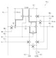
도 2는 본 발명의 일 실시예에 따른 화소(PXij)의 회로도이다. Figure 2 is a circuit diagram of a pixel (PXij) according to an embodiment of the present invention.
도 2에는 도 1에 도시된 j번째 데이터 라인(DLj), i번째 스캔 라인들(GILi, GCLi, GWLi, EBLi) 그리고 i번째 발광 라인(EMLi)에 접속된 화소(PXij)를 예시적으로 도시하였다.FIG. 2 exemplarily shows a pixel (PXij) connected to the j-th data line (DLj), the ith scan lines (GILi, GCLi, GWLi, EBLi), and the i-th emission line (EMLi) shown in FIG. 1. did.
도 1에 도시된 복수의 화소들(PX) 각각은 도 2에 도시된 화소(PXij)와 동일한 회로 구성을 가질 수 있다. 일 실시예에서 화소(PXij)는 발광 소자(ED) 및 화소 회로를 포함한다. 일 실시예에서 발광 소자(ED)는 발광 다이오드(light emitting diode)일 수 있다. 일 실시예에서, 화소(PXij)의 화소 회로는 10개의 트랜지스터들(T1-T10), 제1 커패시터(Cst) 및 제2 커패시터(Chold)를 포함한다. 일 실시예에 따른 화소(PXij)의 회로 구성은 도 2에 제한되지 않는다. 화소(PXij)가 포함하는 트랜지스터들의 개수 및/또는 커패시터들의 개수 그리고 그들의 연결 관계는 다양하게 변형 가능하다.Each of the plurality of pixels PX shown in FIG. 1 may have the same circuit configuration as the pixel PXij shown in FIG. 2. In one embodiment, the pixel PXij includes a light emitting element ED and a pixel circuit. In one embodiment, the light emitting device ED may be a light emitting diode. In one embodiment, the pixel circuit of the pixel PXij includes 10 transistors T1-T10, a first capacitor Cst, and a second capacitor Chold. The circuit configuration of the pixel PXij according to one embodiment is not limited to FIG. 2. The number of transistors and/or capacitors included in the pixel PXij and their connection relationships can be varied in various ways.
일 실시예에서, 제1 내지 제10 트랜지스터들(T1-T10) 각각은 LTPS(low-temperature polycrystalline silicon) 반도체층을 갖는 P-타입 트랜지스터이다. 그러나 본 발명은 이에 한정되는 것은 아니다. 일 실시예에서, 제1 내지 제10 트랜지스터들(T1-T10) 각각은 산화물 반도체를 반도체층으로 하는 N-타입 트랜지스터일 수 있다. 다른 실시예에서, 제1 내지 제10 트랜지스터들(T1-T10) 중 적어도 하나는 N-타입 트랜지스터이고, 나머지는 P-타입 트랜지스터일 수 있다.In one embodiment, each of the first to tenth transistors T1 to T10 is a P-type transistor having a low-temperature polycrystalline silicon (LTPS) semiconductor layer. However, the present invention is not limited to this. In one embodiment, each of the first to tenth transistors T1 to T10 may be an N-type transistor using an oxide semiconductor as a semiconductor layer. In another embodiment, at least one of the first to tenth transistors T1 to T10 may be an N-type transistor, and the others may be P-type transistors.
스캔 라인들(GILi, GCLi, GWLi, EBLi)은 스캔 신호들(GIi, GCi, GWi, EBi)을 각각 전달하고, 발광 라인(EMLi)은 발광 신호(EMi)를 전달할 수 있다. 데이터 라인(DLj)은 데이터 신호(Dj)를 전달한다. 데이터 신호(Dj)는 표시 장치(DD, 도 4 참조)에 입력되는 입력 영상 신호(RGB)에 대응하는 전압 레벨을 가질 수 있다. 제1 내지 제4 구동 전압 라인들(VL1, VL2, VL3, VL4)은 제1 구동 전압(ELVDD), 제2 구동 전압(ELVSS), 제1 초기화 전압(VINT) 및 바이어스 전압(Vbias)을 전달할 수 있다.The scan lines (GILi, GCLi, GWLi, and EBLi) may transmit scan signals (GIi, GCi, GWi, and EBi), respectively, and the emission line (EMLi) may transmit an emission signal (EMi). The data line DLj transmits the data signal Dj. The data signal Dj may have a voltage level corresponding to the input image signal RGB input to the display device DD (see FIG. 4). The first to fourth driving voltage lines (VL1, VL2, VL3, and VL4) transmit the first driving voltage (ELVDD), the second driving voltage (ELVSS), the first initialization voltage (VINT), and the bias voltage (Vbias). You can.
제1 트랜지스터(T1)는 제8 트랜지스터(T8)를 경유하여 제1 구동 전압 라인(VL1)과 연결된 제1 전극, 제6 트랜지스터(T6)를 경유하여 발광 소자(ED)의 애노드(anode)와 전기적으로 연결된 제2 전극, 제1 노드(N1)와 연결된 게이트 전극을 포함한다.The first transistor T1 is connected to the first electrode connected to the first driving voltage line VL1 via the eighth transistor T8, and to the anode of the light emitting element ED via the sixth transistor T6. It includes a second electrode electrically connected and a gate electrode connected to the first node N1.
제2 트랜지스터(T2)는 데이터 라인(DLj)과 연결된 제1 전극, 제2 노드(N2)와 연결된 제2 전극 및 스캔 라인(GWLi)과 연결된 게이트 전극을 포함한다. 제2 트랜지스터(T2)는 스캔 라인(GWLi)을 통해 전달받은 스캔 신호(GWi)에 따라 턴 온되어 데이터 라인(DLj)으로부터 전달된 데이터 신호(Dj)를 제2 노드(N2)로 전달할 수 있다.The second transistor T2 includes a first electrode connected to the data line DLj, a second electrode connected to the second node N2, and a gate electrode connected to the scan line GWLi. The second transistor T2 may be turned on according to the scan signal GWi received through the scan line GWLi and transmit the data signal Dj transmitted from the data line DLj to the second node N2. .
제3 트랜지스터(T3)는 제1 트랜지스터(T1)의 게이트 전극과 연결된 제1 전극, 제1 노드(N1)와 연결된 제2 전극, 스캔 라인(GCLi)과 연결된 게이트 전극을 포함한다. 제3 트랜지스터(T3)는 스캔 라인(GCLi)을 통해 전달받은 스캔 신호(GCi)에 따라 턴 온되어 제1 노드(N1) 즉, 제1 트랜지스터(T1)의 게이트 전극과 제1 트랜지스터(T1)의 제2 전극을 연결할 수 있다.The third transistor T3 includes a first electrode connected to the gate electrode of the first transistor T1, a second electrode connected to the first node N1, and a gate electrode connected to the scan line GCLi. The third transistor T3 is turned on according to the scan signal GCi received through the scan line GCLi to connect the first node N1, that is, the gate electrode of the first transistor T1 and the first transistor T1. The second electrode can be connected.
제4 트랜지스터(T4)는 제1 노드(N1)와 연결된 제1 전극, 제3 구동 전압 라인(VL3)과 연결된 제2 전극 및 스캔 라인(GILi)과 연결된 게이트 전극을 포함한다. 제4 트랜지스터(T4)는 스캔 라인(GILi)을 통해 전달받은 스캔 신호(GIi)에 따라 턴 온되어 제1 초기화 전압(VINT)을 제1 노드(N1) 즉, 제1 트랜지스터(T1)의 게이트 전극에 전달할 수 있다.The fourth transistor T4 includes a first electrode connected to the first node N1, a second electrode connected to the third driving voltage line VL3, and a gate electrode connected to the scan line GILi. The fourth transistor T4 is turned on according to the scan signal GIi received through the scan line GILi and applies the first initialization voltage VINT to the first node N1, that is, the gate of the first transistor T1. It can be delivered to the electrode.
제5 트랜지스터(T5)는 제1 구동 전압 라인(VL1)과 연결된 제1 전극, 제2 노드(N2)와 연결된 제2 전극 및 스캔 라인(GCLi)에 연결된 게이트 전극을 포함한다. 제5 트랜지스터(T5)는 스캔 라인(GCLi)을 통해 전달받은 스캔 신호(GCi)에 따라 턴 온되어 제1 구동 전압(ELVDD)을 제2 노드(N2)에 전달할 수 있다.The fifth transistor T5 includes a first electrode connected to the first driving voltage line VL1, a second electrode connected to the second node N2, and a gate electrode connected to the scan line GCLi. The fifth transistor T5 is turned on according to the scan signal GCi received through the scan line GCLi and can transmit the first driving voltage ELVDD to the second node N2.
제6 트랜지스터(T6)는 제1 트랜지스터(T1)의 제2 전극과 연결된 제1 전극, 발광 소자(ED)의 애노드에 연결된 제2 전극 및 발광 라인(EMLi)에 연결된 게이트 전극을 포함한다.The sixth transistor T6 includes a first electrode connected to the second electrode of the first transistor T1, a second electrode connected to the anode of the light emitting element ED, and a gate electrode connected to the light emitting line EMLi.
제7 트랜지스터(T7)는 발광 소자(ED)의 애노드와 연결된 제1 전극, 제3 구동 전압 라인(VL3)과 연결된 제2 전극 및 스캔 라인(EBLi)과 연결된 게이트 전극을 포함한다. 제7 트랜지스터(T7)는 스캔 라인(EBLi)을 통해 전달받은 스캔 신호(EBi)에 따라 턴 온되어 발광 소자(ED)의 애노드를 제3 구동 전압 라인(VL3)의 제1 초기화 전압(VINT)으로 초기화할 수 있다.The seventh transistor T7 includes a first electrode connected to the anode of the light emitting device ED, a second electrode connected to the third driving voltage line VL3, and a gate electrode connected to the scan line EBLi. The seventh transistor T7 is turned on according to the scan signal EBi received through the scan line EBLi to connect the anode of the light emitting device ED to the first initialization voltage VINT of the third driving voltage line VL3. It can be initialized with .
제8 트랜지스터(T8)는 제1 구동 전압 라인(VL1)과 연결된 제1 전극, 제1 트랜지스터(T1)의 제1 전극과 연결된 제2 전극 및 발광 라인(EMLi)에 연결된 게이트 전극을 포함한다.The eighth transistor T8 includes a first electrode connected to the first driving voltage line VL1, a second electrode connected to the first electrode of the first transistor T1, and a gate electrode connected to the light emission line EMLi.
제6 트랜지스터(T6) 및 제8 트랜지스터(T8) 각각은 발광 라인(EMLi)을 통해 전달받은 발광 신호(EMi)에 따라 동시에 턴 온될 수 있다. 제6 트랜지스터(T6) 및 제8 트랜지스터(T8)가 턴 온되면, 제8 트랜지스터(T8), 제1 트랜지스터(T1) 및 제6 트랜지스터(T6)를 통해 제1 구동 전압 라인(VL1)과 발광 소자(ED) 사이에 전류 경로가 형성될 수 있다.Each of the sixth transistor T6 and the eighth transistor T8 may be turned on simultaneously according to the light emission signal EMi received through the light emission line EMLi. When the sixth transistor T6 and the eighth transistor T8 are turned on, the first driving voltage line VL1 and light are emitted through the eighth transistor T8, the first transistor T1, and the sixth transistor T6. A current path may be formed between the elements ED.
제9 트랜지스터(T9)는 제4 구동 전압 라인(VL4)과 연결된 제1 전극, 제1 트랜지스터(T1)의 제1 전극과 연결된 제2 전극 및 스캔 라인(EBLi)에 연결된 게이트 전극을 포함한다. 제9 트랜지스터(T9)는 스캔 라인(EBLi)을 통해 전달받은 스캔 신호(EBi)에 따라 턴 온되어 바이어스 전압(Vbias)을 제1 트랜지스터(T1)의 제1 전극에 전달할 수 있다.The ninth transistor T9 includes a first electrode connected to the fourth driving voltage line VL4, a second electrode connected to the first electrode of the first transistor T1, and a gate electrode connected to the scan line EBLi. The ninth transistor T9 is turned on according to the scan signal EBi received through the scan line EBLi and can transmit the bias voltage Vbias to the first electrode of the first transistor T1.
제10 트랜지스터(T10)는 제1 구동 전압 라인(VL1)과 연결된 제1 전극, 제1 트랜지스터(T1)의 제1 전극과 연결된 제2 전극 및 스캔 라인(GCLi)에 연결된 게이트 전극을 포함한다. 제10 트랜지스터(T10)는 스캔 라인(GCLi)을 통해 전달받은 스캔 신호(GCi)에 따라 턴 온되어 제1 구동 전압(ELVDD)을 제1 트랜지스터(T1)의 제1 전극에 전달할 수 있다.The tenth transistor T10 includes a first electrode connected to the first driving voltage line VL1, a second electrode connected to the first electrode of the first transistor T1, and a gate electrode connected to the scan line GCLi. The tenth transistor T10 is turned on according to the scan signal GCi received through the scan line GCLi and can transmit the first driving voltage ELVDD to the first electrode of the first transistor T1.
제1 커패시터(Cst)는 제1 노드(N1)와 제2 노드(N2) 사이에 연결된다. 제2 커패시터(Chold)는 제1 구동 전압 라인(VL1)과 제2 노드(N2) 사이에 연결된다.The first capacitor Cst is connected between the first node N1 and the second node N2. The second capacitor Chold is connected between the first driving voltage line VL1 and the second node N2.
도 3a 및 도 3b 각각은 표시 장치의 동작을 설명하기 위한 타이밍도이다.FIGS. 3A and 3B are timing diagrams for explaining the operation of the display device.
도 1, 도 2, 도 3a 및 도 3b를 참조하면, 이하 설명에서 표시 장치(DD)는 제1 구동 주파수(예를 들면, 240Hz) 및 제2 구동 주파수(예를 들면, 120Hz)로 동작하는 것을 일 예로 설명하나, 본 발명은 이에 한정되지 않는다. 표시 장치(DD)의 구동 주파수는 다양하게 변경될 수 있다. 일 실시예에서, 표시 장치(DD)의 구동 주파수는 제1 구동 주파수 및 제2 구동 주파수 중 어느 하나로 선택될 수 있다. 또한 표시 장치(DD)는 동작 중 구동 주파수를 특정 주파수로 고정하지 않고, 구동 주파수가 수시로 변경되는 가변 주파수 모드로 동작할 수 있다. 일 실시예에서, 표시 장치(DD)의 구동 주파수는 입력 영상 신호(I_RGB)의 주파수 및/또는 제어 신호(CTRL)에 따라서 결정될 수 있다.Referring to FIGS. 1, 2, 3A, and 3B, in the following description, the display device DD operates at a first driving frequency (eg, 240 Hz) and a second driving frequency (eg, 120 Hz). This is explained as an example, but the present invention is not limited thereto. The driving frequency of the display device DD can be changed in various ways. In one embodiment, the driving frequency of the display device DD may be selected as one of a first driving frequency and a second driving frequency. Additionally, the display device DD may operate in a variable frequency mode in which the driving frequency is frequently changed rather than fixing the driving frequency to a specific frequency during operation. In one embodiment, the driving frequency of the display device DD may be determined according to the frequency of the input image signal I_RGB and/or the control signal CTRL.
구동 컨트롤러(100)는 제어 신호(CTRL)에 응답해서 제1 스캔 제어 신호(SCS1) 및 제2 스캔 제어 신호(SCS2)를 제1 구동 회로(300) 및 제2 구동 회로(400)로 각각 제공한다. 제어 신호(CTRL)는 동기 신호(V_SYNC)를 포함할 수 있다. 제1 구동 회로(300) 및 제2 구동 회로(400)는 제1 스캔 제어 신호(SCS1) 및 제2 스캔 제어 신호(SCS2)에 각각 응답해서 구동 주파수에 대응하는 스캔 신호들을 출력할 수 있다.The
도 3a 및 도 3b에 도시된 스캔 신호들(GW1-GWn)은 도 1에 도시된 스캔 라인들(GWL1-GWLn)로 각각 제공되고, 스캔 신호들(EB1-EBn)은 도 1에 도시된 스캔 라인들(EBL1-EBLn)로 각각 제공될 수 있다.The scan signals (GW1-GWn) shown in FIGS. 3A and 3B are respectively provided to the scan lines (GWL1-GWLn) shown in FIG. 1, and the scan signals (EB1-EBn) are provided by the scan lines (GWL1-GWLn) shown in FIG. 1. Each may be provided as lines (EBL1-EBLn).
도 3a는 표시 장치(DD)의 구동 주파수가 제1 구동 주파수(예를 들면, 240Hz)일 때 시작 신호 및 스캔 신호들의 타이밍도이다.FIG. 3A is a timing diagram of start signals and scan signals when the driving frequency of the display device DD is a first driving frequency (eg, 240 Hz).
도 1 및 도 3a를 참조하면, 구동 주파수가 제1 구동 주파수(예를 들면, 240Hz)일 때 프레임들(F11, F12) 각각은 1개의 쓰기 구간(WP) 및 1개의 홀드 구간(HP)을 포함할 수 있다. 동기 신호(V_SYNC)는 쓰기 구간(WP) 및 홀드 구간(HP) 각각의 시작을 나타내는 신호일 수 있다.Referring to FIGS. 1 and 3A, when the driving frequency is a first driving frequency (e.g., 240 Hz), each of the frames F11 and F12 has one write section (WP) and one hold section (HP). It can be included. The synchronization signal (V_SYNC) may be a signal indicating the start of each write period (WP) and hold period (HP).
제1 구동 회로(300) 및 제2 구동 회로(400)는 프레임들(F11, F12) 각각의 쓰기 구간(WP)에서 스캔 신호들(GW1-GWn)을 순차적으로 활성 레벨(예를 들면, 로우 레벨)로 활성화하고, 스캔 신호들(EB1-EBn)을 순차적으로 로우 레벨로 활성화한다. 도 3a에는 스캔 신호들(GW1-GWn) 및 스캔 신호들(EB1-EBn)만 도시되었으나, 스캔 라인들(GCL1-GCLn, GBL1-GBLn)로 제공되는 스캔 신호들 및 발광 라인들(EML1-EMLn)로 제공되는 발광 신호들도 프레임들(F11, F12) 각각의 쓰기 구간(WP)에서 순차적으로 활성화될 수 있다.The
제1 구동 회로(300) 및 제2 구동 회로(400)는 홀드 구간(HP)동안 스캔 신호들(GW1-GWn)을 비활성 레벨(예를 들면, 하이 레벨)로 유지하고, 스캔 신호들(EB1-EBn)을 순차적으로 활성화할 수 있다. 도 3a에 도시되지 않았으나, 제1 구동 회로(300) 및 제2 구동 회로(400)는 홀드 구간(HP)동안 스캔 신호들(GW1-GWn)과 동일하게 스캔 라인들(GCL1-GCLn, GBL1-GBLn)로 제공되는 스캔 신호들 및 발광 라인들(EML1-EMLn)로 제공되는 발광 신호들을 비활성 레벨(예를 들면, 하이 레벨)로 유지할 수 있다.The
제1 구동 회로(300) 및 제2 구동 회로(400)는 홀드 구간(HP)동안 스캔 신호들(GB1-GBn)을 순차적으로 활성화할 수 있다. 다시 말하면, 프레임들(F11, F12) 각각의 홀드 구간(HP)동안 스캔 신호들(GB1-GBn)만 순차적으로 활성화하고, 다른 스캔 신호들 및 발광 신호들을 비활성 레벨로 유지할 수 있다.The
도 3b는 표시 장치(DD)의 구동 주파수가 제2 구동 주파수(예를 들면, 120Hz)일 때 시작 신호 및 스캔 신호들의 타이밍도이다.FIG. 3B is a timing diagram of start signals and scan signals when the driving frequency of the display device DD is a second driving frequency (eg, 120 Hz).
도 1 및 도 3b를 참조하면, 구동 주파수가 제2 구동 주파수(예를 들면, 120Hz)일 때 프레임(F21)의 주기(또는 지속 시간)는 도 3a에 도시된 프레임들(F11, F12) 각각의 주기의 2배일 수 있다. 프레임(F21)은 1개의 쓰기 구간(WP)과 3개의 홀드 구간들(HP)을 포함할 수 있다. 제1 구동 회로(300) 및 제2 구동 회로(400)는 프레임(F21)의 쓰기 구간(WP)동안 스캔 신호들(GW1-GWn)을 순차적으로 로우 레벨로 활성화하고, 스캔 신호들(EB1-EBn)을 순차적으로 로우 레벨로 활성화한다. 도 3b에는 스캔 신호들(GW1-GWn) 및 스캔 신호들(EB1-EBn)만 도시되었으나, 스캔 라인들(GCL1-GCLn, GBL1-GBLn)로 제공되는 스캔 신호들 및 발광 라인들(EML1-EMLn)로 제공되는 발광 신호들도 프레임들(F11, F12) 각각의 쓰기 구간(WP)에서 순차적으로 활성화될 수 있다.Referring to FIGS. 1 and 3B, when the driving frequency is a second driving frequency (for example, 120 Hz), the period (or duration) of the frame F21 is the frame F11 and F12 shown in FIG. 3A, respectively. It may be twice the period of . The frame F21 may include one write section (WP) and three hold sections (HP). The
제1 구동 회로(300) 및 제2 구동 회로(400)는 홀드 구간(HP)동안 스캔 신호들(GW1-GWn)을 비활성 레벨(예를 들면, 하이 레벨)로 유지하고, 스캔 신호들(EB1-EBn)을 순차적으로 활성화할 수 있다. 도 3b에 도시되지 않았으나, 제1 구동 회로(300) 및 제2 구동 회로(400)는 홀드 구간(HP)동안 스캔 신호들(GW1-GWn)과 동일하게 스캔 라인들(GCL1-GCLn, GBL1-GBLn)로 제공되는 스캔 신호들 및 발광 라인들(EML1-EMLn)로 제공되는 발광 신호들을 비활성 레벨(예를 들면, 하이 레벨)로 유지할 수 있다.The
제1 구동 회로(300) 및 제2 구동 회로(400)는 홀드 구간(HP)동안 스캔 신호들(GB1-GBn)을 순차적으로 활성화할 수 있다. 다시 말하면, 프레임(F21)의 3개의 홀드 구간들(HP) 각각에서 스캔 신호들(GB1-GBn)만 순차적으로 활성화하고, 다른 스캔 신호들 및 발광 신호들을 비활성 레벨로 유지할 수 있다.The
도 4a는 쓰기 구간(WP)동안 화소의 동작을 설명하기 위한 타이밍도이다.FIG. 4A is a timing diagram for explaining the operation of a pixel during a writing period (WP).
도 4b는 홀드 구간(HP)동안 화소의 동작을 설명하기 위한 타이밍도이다.Figure 4b is a timing diagram to explain the operation of the pixel during the hold period (HP).
도 4a에 도시된 것과 같이, 쓰기 구간(WP)은 제1 내지 제7 구간들(P1, P2, P3, P4, P5, P6, P7)을 포함할 수 있다. 도 4b에 도시된 것과 같이, 홀드 구간(HP)은 제8 구간(P8)을 포함할 수 있다.As shown in FIG. 4A, the writing section WP may include first to seventh sections P1, P2, P3, P4, P5, P6, and P7. As shown in FIG. 4B, the hold section HP may include an eighth section P8.
도 5a, 도 5b, 도 5c, 도 5d, 도 5e, 도 5f, 도 5g 및 도 5h는 화소의 동작을 설명하기 위한 도면들이다.FIGS. 5A, 5B, 5C, 5D, 5E, 5F, 5G, and 5H are diagrams for explaining the operation of a pixel.
도 4a 및 도 5a를 참조하면, 쓰기 구간(WP)의 제1 구간(P1)동안 스캔 신호들(GCi, GWi, EBi) 및 발광 신호(EMi)는 각각 비활성 레벨(예를 들면, 하이 레벨)이고, 스캔 신호(GIi)는 활성 레벨(예를 들면, 로우 레벨)이다. 활성 레벨의 스캔 신호(GIi)에 응답해서 제4 트랜지스터(T4)가 턴 온 된다. 그러므로 제1 구간(P1)동안 초기화 전압(VINT)은 제4 트랜지스터(T4)를 통해 제1 노드(N1)로 전달될 수 있다. 제1 구간(P1)은 제1 노드(N1) 즉, 제1 트랜지스터(T1)의 게이트 전극을 초기화 전압(VINT)으로 초기화하는 제1 초기화 구간일 수 있다.Referring to FIGS. 4A and 5A, during the first section P1 of the writing section WP, the scan signals GCi, GWi, and EBi and the emission signal EMi are each at an inactive level (e.g., high level). and the scan signal GIi is at an active level (eg, low level). The fourth transistor T4 is turned on in response to the scan signal GIi at the active level. Therefore, during the first period P1, the initialization voltage VINT may be transmitted to the first node N1 through the fourth transistor T4. The first section P1 may be a first initialization section in which the first node N1, that is, the gate electrode of the first transistor T1, is initialized to the initialization voltage VINT.
도 4a 및 도 5b를 참조하면, 쓰기 구간(WP)의 제2 구간(P2)동안 스캔 신호들(GIi, GWi, EBi) 및 발광 신호(EMi)는 각각 비활성 레벨(예를 들면, 하이 레벨)이고, 스캔 신호(GCi)는 활성 레벨(예를 들면, 로우 레벨)이다. 활성 레벨의 스캔 신호(GCi)에 응답해서 제3 트랜지스터(T3), 제5 트랜지스터(T5) 및 제10 트랜지스터(T10)가 각각 턴 온 된다.Referring to FIGS. 4A and 5B, during the second section (P2) of the writing section (WP), the scan signals (GIi, GWi, EBi) and the emission signal (EMi) are each at an inactive level (e.g., high level). , and the scan signal GCi is at an active level (eg, low level). In response to the scan signal GCi at the active level, the third transistor T3, the fifth transistor T5, and the tenth transistor T10 are respectively turned on.
제3 트랜지스터(T3) 및 제10 트랜지스터(T10)가 턴 온 됨에 따라 제10 트랜지스터(T10), 제1 트랜지스터(T1) 및 제3 트랜지스터(T3)를 통해 제1 구동 전압(ELVDD)이 제1 노드(N1)로 전달될 수 있다. 제1 트랜지스터(T1)의 게이트 전극으로 제공된 전압은 제1 구동 전압(ELVDD)에서 제1 트랜지스터(T1)의 스레숄드 전압(이하, Vth라 칭함)만큼 낮아진 전압일 수 있다(ELVDD-Vth).As the third transistor T3 and the tenth transistor T10 are turned on, the first driving voltage ELVDD becomes the first through the tenth transistor T10, the first transistor T1, and the third transistor T3. It can be transmitted to node N1. The voltage provided to the gate electrode of the first transistor T1 may be a voltage lowered from the first driving voltage ELVDD to the threshold voltage (hereinafter referred to as Vth) of the first transistor T1 (ELVDD-Vth).
제2 구간(P2)은 제1 트랜지스터(T1)의 스레숄드 전압(Vth)을 보상하기 위한 제1 보상 구간일 수 있다.The second section P2 may be a first compensation section for compensating the threshold voltage Vth of the first transistor T1.
한편, 제5 트랜지스터(T5)가 턴 온 됨에 따라 제5 트랜지스터(T5)를 통해 제1 구동 전압(ELVDD)이 제2 노드(N2)로 전달될 수 있다.Meanwhile, as the fifth transistor T5 is turned on, the first driving voltage ELVDD may be transmitted to the second node N2 through the fifth transistor T5.
제2 노드(N2)의 전압(Va)은 이전 프레임에서 데이터 라인(DLj)으로 제공된 데이터 신호(Dj)의 전압(Vdata라 칭함)에서 제1 구동 전압(ELVDD)으로 변경된다. 제2 노드(N2)의 전압(Va)의 변화량은 제1 커패시터(Cst)의 커플링에 의해 제1 노드(N1)로 전달될 수 있다. 즉, 제1 노드(N1)의 전압 레벨은 이전 프레임에서의 데이터 신호(Dj)의 전압(Vdata)에 영향을 받을 수 있다.The voltage Va of the second node N2 changes from the voltage (referred to as Vdata) of the data signal Dj provided to the data line DLj in the previous frame to the first driving voltage ELVDD. The change in voltage Va of the second node N2 may be transmitted to the first node N1 through coupling of the first capacitor Cst. That is, the voltage level of the first node N1 may be affected by the voltage Vdata of the data signal Dj in the previous frame.
도 4a 및 도 5c를 참조하면, 쓰기 구간(WP)의 제3 구간(P3)동안 스캔 신호들(GCi, GWi, EBi) 및 발광 신호(EMi)는 각각 비활성 레벨(예를 들면, 하이 레벨)이고, 스캔 신호(GIi)는 활성 레벨(예를 들면, 로우 레벨)이다. 활성 레벨의 스캔 신호(GIi)에 응답해서 제4 트랜지스터(T4)가 턴 온 된다. 그러므로 제1 구간(P1)동안 초기화 전압(VINT)은 제4 트랜지스터(T4)를 통해 제1 노드(N1)로 전달될 수 있다. 제1 구간(P1)은 제1 노드(N1) 즉, 제1 트랜지스터(T1)의 게이트 전극을 초기화 전압(VINT)으로 초기화하는 제2 초기화 구간일 수 있다.Referring to FIGS. 4A and 5C, during the third section (P3) of the writing section (WP), the scan signals (GCi, GWi, EBi) and the emission signal (EMi) are each at an inactive level (e.g., high level). and the scan signal GIi is at an active level (eg, low level). The fourth transistor T4 is turned on in response to the scan signal GIi at the active level. Therefore, during the first period P1, the initialization voltage VINT may be transmitted to the first node N1 through the fourth transistor T4. The first section P1 may be a second initialization section in which the first node N1, that is, the gate electrode of the first transistor T1, is initialized to the initialization voltage VINT.
도 4a 및 도 5d를 참조하면, 쓰기 구간(WP)의 제4 구간(P4)동안 스캔 신호들(GIi, GWi, EBi) 및 발광 신호(EMi)는 각각 비활성 레벨(예를 들면, 하이 레벨)이고, 스캔 신호(GCi)는 활성 레벨(예를 들면, 로우 레벨)이다. 활성 레벨의 스캔 신호(GCi)에 응답해서 제3 트랜지스터(T3), 제5 트랜지스터(T5) 및 제10 트랜지스터(T10)가 각각 턴 온 된다.Referring to FIGS. 4A and 5D, during the fourth section (P4) of the writing section (WP), the scan signals (GIi, GWi, EBi) and the emission signal (EMi) are each at an inactive level (e.g., high level). , and the scan signal GCi is at an active level (eg, low level). In response to the scan signal GCi at the active level, the third transistor T3, the fifth transistor T5, and the tenth transistor T10 are respectively turned on.
제3 트랜지스터(T3) 및 제10 트랜지스터(T10)가 턴 온 됨에 따라 제10 트랜지스터(T10), 제1 트랜지스터(T1) 및 제3 트랜지스터(T3)를 통해 제1 구동 전압(ELVDD)이 제1 노드(N1)로 전달될 수 있다. 제1 트랜지스터(T1)의 게이트 전극으로 제공된 전압은 제1 구동 전압(ELVDD)에서 제1 트랜지스터(T1)의 스레숄드 전압(이하, Vth라 칭함)만큼 낮아진 전압일 수 있다(ELVDD-Vth).As the third transistor T3 and the tenth transistor T10 are turned on, the first driving voltage ELVDD becomes the first through the tenth transistor T10, the first transistor T1, and the third transistor T3. It can be transmitted to node N1. The voltage provided to the gate electrode of the first transistor T1 may be a voltage lowered from the first driving voltage ELVDD to the threshold voltage (hereinafter referred to as Vth) of the first transistor T1 (ELVDD-Vth).
제2 구간(P2)은 제1 트랜지스터(T1)의 스레숄드 전압(Vth)을 보상하기 위한 제2 보상 구간일 수 있다.The second section P2 may be a second compensation section for compensating the threshold voltage Vth of the first transistor T1.
한편, 제5 트랜지스터(T5)가 턴 온 됨에 따라 제5 트랜지스터(T5)를 통해 제1 구동 전압(ELVDD)이 제2 노드(N2)로 전달될 수 있다.Meanwhile, as the fifth transistor T5 is turned on, the first driving voltage ELVDD may be transmitted to the second node N2 through the fifth transistor T5.
제2 노드(N2)의 전압(Va)은 제2 구간(P2)에서 제1 구동 전압(ELVDD)이었고, 제4 구간(P4)에서 다시 제5 트랜지스터(T5)를 통해 제1 구동 전압(ELVDD)이 공급된다. 그러므로 제2 노드(N2)의 전압(Va)의 전압 레벨 변화는 없다.The voltage (Va) of the second node (N2) was the first driving voltage (ELVDD) in the second section (P2), and the first driving voltage (ELVDD) again through the fifth transistor (T5) in the fourth section (P4). ) is supplied. Therefore, there is no change in the voltage level of the voltage Va of the second node N2.
이와 같이, 제2 구간(P2)과 제4 구간(P4)에서 제1 구동 전압(ELVDD)을 2회 제2 노드(N2)로 제공함으로써 이전 프레임에서의 데이터 신호(Dj)의 전압(Vdata)이 제1 노드(N1)에 영향을 주는 것을 제거할 수 있다.In this way, the first driving voltage ELVDD is provided to the second node N2 twice in the second section P2 and the fourth section P4, thereby increasing the voltage Vdata of the data signal Dj in the previous frame. Anything affecting this first node (N1) can be removed.
도 4a 및 도 5e를 참조하면, 쓰기 구간(WP)의 제5 구간(P5)동안 스캔 신호(GWi)만 활성 레벨이다. 활성 레벨의 스캔 신호(GWi)에 의해 제2 트랜지스터(T2)가 턴 온되면 데이터 라인(DLj)로부터의 데이터 신호(Dj)가 제2 노드(N2)로 전달될 수 있다.Referring to FIGS. 4A and 5E, only the scan signal GWi is at an active level during the fifth section P5 of the write section WP. When the second transistor T2 is turned on by the active level scan signal GWi, the data signal Dj from the data line DLj may be transmitted to the second node N2.
제2 노드(N2)의 전압은 제1 구동 전압(ELVDD)에서 데이터 신호(Dj)의 전압(Vdata)으로 변경된다. 제2 노드(N2)의 전압 변화량 "Vdata-ELVDD"가 제1 커패시터(Cst)의 커플링에 의해 제1 노드(N1)로 전달될 수 있다.The voltage of the second node N2 changes from the first driving voltage ELVDD to the voltage Vdata of the data signal Dj. The voltage change “Vdata-ELVDD” of the second node N2 may be transmitted to the first node N1 through coupling of the first capacitor Cst.
제4 구간(P4)에서 제1 노드(N1)의 전압은 "ELVDD-Vth"이었으므로, 제5 구간(P5)에서 제1 노드(N1) 즉, 제1 트랜지스터(T1)의 게이트 전극의 전압은 "ELVDD-Vth + (Vdata-ELVDD)"으로 된다.Since the voltage of the first node (N1) in the fourth section (P4) was “ELVDD-Vth”, the voltage of the first node (N1), that is, the gate electrode of the first transistor (T1) in the fifth section (P5) It becomes “ELVDD-Vth + (Vdata-ELVDD)”.
제5 구간(P5)은 데이터 신호(Dj)에 대응하는 전압을 제1 커패시터(Cst)에 저장하는 데이터 쓰기 구간일 수 있다.The fifth section P5 may be a data writing section in which the voltage corresponding to the data signal Dj is stored in the first capacitor Cst.
도 4a 및 도 5f를 참조하면, 쓰기 구간(WP)의 제6 구간(P6)동안 스캔 신호들(GIi, GCi, GWi) 및 발광 신호(EMi)가 각각 비활성 레벨이고, 스캔 신호(EBi)는 활성 레벨이다.Referring to FIGS. 4A and 5F, the scan signals (GIi, GCi, GWi) and the emission signal (EMi) are each at an inactive level during the sixth section (P6) of the writing section (WP), and the scan signal (EBi) is at an inactive level. This is the active level.
활성 레벨의 스캔 신호(EBi)에 의해서 제7 트랜지스터(T7) 및 제9 트랜지스터(T9)가 각각 턴 온될 수 있다. 발광 소자(ED)의 애노드에는 제7 트랜지스터(T7)를 통해 초기화 전압(VINT)이 제공된다. 제1 트랜지스터(T1)의 제1 전극에는 제4 트랜지스터(T4)를 통해 바이어스 전압(Vbias)이 제공된다.The seventh transistor T7 and the ninth transistor T9 may each be turned on by the scan signal EBi at the active level. An initialization voltage (VINT) is provided to the anode of the light emitting device (ED) through the seventh transistor (T7). A bias voltage (Vbias) is provided to the first electrode of the first transistor (T1) through the fourth transistor (T4).
제1 트랜지스터(T1)의 제1 전극에 바이어스 전압(Vbias)을 제공함으로써 제1 트랜지스터(T1)의 스레숄드 전압(Vth) 특성 변화에 따른 히스테리시스 영향을 최소화할 수 있다.By providing a bias voltage (Vbias) to the first electrode of the first transistor (T1), the hysteresis effect due to a change in the threshold voltage (Vth) characteristics of the first transistor (T1) can be minimized.
제6 구간(P6)은 발광 소자(ED)의 애노드 및 제1 트랜지스터(T1)의 제1 전극을 초기화하는 애노드 초기화 및 바이어스 구간일 수 있다.The sixth section P6 may be an anode initialization and bias section that initializes the anode of the light emitting device ED and the first electrode of the first transistor T1.
도 4a 및 도 5g를 참조하면, 쓰기 구간(WP)의 제7 구간(P7)동안 스캔 신호들(GIi, GCi, GWi, EBi)은 모두 비활성 레벨이고, 발광 신호(EMi)는 활성 레벨이다. 활성 레벨의 발광 신호(EMi)에 의해서 제6 트랜지스터(T6) 및 제8 트랜지스터(T8)가 각각 턴 온될 수 있다.Referring to FIGS. 4A and 5G, during the seventh section P7 of the writing section WP, the scan signals GIi, GCi, GWi, and EBi are all at inactive levels, and the emission signal EMi is at an active level. The sixth transistor T6 and the eighth transistor T8 may each be turned on by the light emission signal EMi at the active level.
제6 트랜지스터(T6) 및 제8 트랜지스터(T8)가 턴 온되면, 제8 트랜지스터(T8), 제1 트랜지스터(T1) 및 제6 트랜지스터(T6)를 통해 제1 구동 전압 라인(VL1)부터 발광 소자(ED)까지 전류 경로가 형성될 수 있다.When the sixth transistor T6 and the eighth transistor T8 are turned on, light is emitted from the first driving voltage line VL1 through the eighth transistor T8, the first transistor T1, and the sixth transistor T6. A current path may be formed up to the device ED.
이 때, 제1 노드(N1) 즉, 제1 트랜지스터(T1)의 게이트 전극의 전압 레벨에 따라 발광 소자(ED)로 전달되는 전류의 양이 결정될 수 있다. 제5 구간(P5)에서 제1 트랜지스터(T1)의 게이트 전극의 전압은 "ELVDD-Vth + (Vdata-ELVDD)"이었다.At this time, the amount of current transmitted to the light emitting device ED may be determined according to the voltage level of the first node N1, that is, the gate electrode of the first transistor T1. In the fifth section P5, the voltage of the gate electrode of the first transistor T1 was “ELVDD-Vth + (Vdata-ELVDD).”
제1 트랜지스터(T1)를 통해 흐르는 전류는 제1 트랜지스터(T1)의 제1 전극과 게이트 전극 간의 전압 차(Vgs라 칭함)와 제1 트랜지스터(T1)의 스레숄드 전압(Vth)의 차의 제곱 "(Vgs-Vth)2"에 비례한다.The current flowing through the first transistor T1 is the square of the difference between the voltage difference between the first electrode and the gate electrode of the first transistor T1 (referred to as Vgs) and the threshold voltage (Vth) of the first transistor T1. (Vgs-Vth) Proportional to 2 ".
제1 트랜지스터(T1)의 제1 전극의 전압은 제1 구동 전압(ELVDD)이고, 제1 트랜지스터(T1)의 게이트 전극의 전압은 "ELVDD-Vth+(Vdata-ELVDD)"이므로 제1 트랜지스터(T1)의 제1 전극과 게이트 전극 간의 전압 차(Vgs)는 "ELVDD-(ELVDD-Vth+(Vdata-ELVDD))"이다.The voltage of the first electrode of the first transistor (T1) is the first driving voltage (ELVDD), and the voltage of the gate electrode of the first transistor (T1) is “ELVDD-Vth+(Vdata-ELVDD)”, so the first transistor (T1) ) The voltage difference (Vgs) between the first electrode and the gate electrode is “ELVDD-(ELVDD-Vth+(Vdata-ELVDD))”.
그러므로 제1 트랜지스터(T1)를 통해 흐르는 전류는 "(ELVDD-(ELVDD-Vth+(Vdata-ELVDD)-Vth))2"에 비례한다. 즉, 제1 트랜지스터(T1)를 통해 흐르는 전류는 "(ELVDD-Vdata)2"에 비례한다.Therefore, the current flowing through the first transistor T1 is proportional to "(ELVDD-(ELVDD-Vth+(Vdata-ELVDD)-Vth)) 2 ". That is, the current flowing through the first transistor T1 is proportional to "(ELVDD-Vdata) 2 ".
따라서 제1 트랜지스터(T1)의 스레숄드 전압(Vth)의 영향을 제거하고, 데이터 신호(Dj)의 전압(Vata)에 비례하는 전류가 발광 소자(ED)로 제공될 수 있다. 제7 구간(P7)은 발광 소자(ED)가 발광하는 발광 구간일 수 있다.Accordingly, the influence of the threshold voltage (Vth) of the first transistor (T1) can be removed, and a current proportional to the voltage (Vata) of the data signal (Dj) can be provided to the light emitting device (ED). The seventh section P7 may be a light-emitting section in which the light-emitting device ED emits light.
도 4b 및 도 5h를 참조하면, 홀드 구간(HP)의 제8 구간(P8)동안 스캔 신호들(GIi, GCi, GWi) 및 발광 신호(EMi)가 각각 비활성 레벨이고, 스캔 신호(EBi)는 활성 레벨이다.Referring to FIGS. 4B and 5H, the scan signals (GIi, GCi, GWi) and the emission signal (EMi) are each at an inactive level during the eighth section (P8) of the hold section (HP), and the scan signal (EBi) is at an inactive level. This is the active level.
활성 레벨의 스캔 신호(EBi)에 의해서 제7 트랜지스터(T7) 및 제9 트랜지스터(T9)가 각각 턴 온될 수 있다. 발광 소자(ED)의 애노드에는 제7 트랜지스터(T7)를 통해 초기화 전압(VINT)이 제공된다. 제1 트랜지스터(T1)의 제1 전극에는 제4 트랜지스터(T4)를 통해 바이어스 전압(Vbias)이 제공된다.The seventh transistor T7 and the ninth transistor T9 may each be turned on by the scan signal EBi at the active level. An initialization voltage (VINT) is provided to the anode of the light emitting device (ED) through the seventh transistor (T7). A bias voltage (Vbias) is provided to the first electrode of the first transistor (T1) through the fourth transistor (T4).
제1 트랜지스터(T1)의 제1 전극에 바이어스 전압(Vbias)을 제공함으로써 제1 트랜지스터(T1)의 스레숄드 전압(Vth) 특성 변화에 따른 히스테리시스 영향을 최소화할 수 있다.By providing a bias voltage (Vbias) to the first electrode of the first transistor (T1), the hysteresis effect due to a change in the threshold voltage (Vth) characteristics of the first transistor (T1) can be minimized.
도 3a에 도시된 것과 같이, 표시 장치(DD)의 구동 주파수가 제1 구동 주파수일 때 프레임들(F11, F12) 각각은 1개의 홀드 구간(HP)을 포함한다.As shown in FIG. 3A, when the driving frequency of the display device DD is the first driving frequency, each of the frames F11 and F12 includes one hold period HP.
도 3b에 도시된 것과 같이, 표시 장치(DD)의 구동 주파수가 제2 구동 주파수일 때 프레임(F21)은 3개의 홀드 구간들(HP)을 포함한다. 홀드 구간들(HP)에는 데이터 신호(Dj)가 제공되지 않으므로, 한 프레임 내 홀드 구간들(HP)의 개수가 증가하면 제1 트랜지스터(T1)의 스레숄드 전압(Vth) 특성이 변화할 수 있다.As shown in FIG. 3B, when the driving frequency of the display device DD is the second driving frequency, the frame F21 includes three hold sections HP. Since the data signal Dj is not provided to the hold sections HP, when the number of hold sections HP within one frame increases, the threshold voltage Vth characteristics of the first transistor T1 may change.
도 4b 및 도 5h에 도시된 것과 같이, 홀드 구간(HP)의 제8 구간(P8)동안 제1 트랜지스터(T1)의 제1 전극으로 바이어스 전압(Vbias)을 제공함으로써 제1 트랜지스터(T1)의 스레숄드 전압(Vth) 특성 변화에 따른 히스테리시스 영향을 최소화할 수 있다.As shown in FIGS. 4B and 5H, the bias voltage (Vbias) is provided to the first electrode of the first transistor (T1) during the eighth period (P8) of the hold period (HP). Hysteresis effects due to changes in threshold voltage (Vth) characteristics can be minimized.
제8 구간(P8)은 제1 트랜지스터(T1)의 히스테리시스 특성을 보상하는 히스테리시스 보상 구간일 수 있다.The eighth section P8 may be a hysteresis compensation section that compensates for the hysteresis characteristics of the first transistor T1.
일 실시예에서, 도 4a에 도시된 제5 구간(P5)은 1 수평 주기일 수 있다. 1 수평 주기는 표시 패널(DP, 도 1 참조)의 한 행의 화소들(PX)로 데이터 신호(Dj)를 제공하는 시간일 수 있다. 도 4a에 도시된 제2 구간(P2) 및 제4 구간(P4) 즉, 제1 보상 구간 및 제2 보상 구간 각각은 1 수평 주기보다 긴 시간일 수 있다. 제2 구간(P2) 및 제4 구간(P4)이 1 수평 주기보다 긴 시간이므로 표시 장치(DD)의 구동 주파수가 높아지더라도 제1 트랜지스터(T1)의 스레숄드 전압(Vth)을 보상하는 시간을 충분히 확보할 수 있다. 따라서 화소(PXij)는 높은 구동 주파수에서 안정적으로 동작할 수 있다.In one embodiment, the fifth section P5 shown in FIG. 4A may be one horizontal period. One horizontal period may be the time for providing the data signal Dj to one row of pixels PX of the display panel DP (see FIG. 1). The second section P2 and the fourth section P4 shown in FIG. 4A, that is, the first compensation section and the second compensation section, may each be longer than one horizontal period. Since the second section (P2) and the fourth section (P4) are longer than one horizontal period, even if the driving frequency of the display device (DD) increases, the time to compensate for the threshold voltage (Vth) of the first transistor (T1) is sufficient. It can be secured. Therefore, the pixel PXij can operate stably at a high driving frequency.
화소(PXij)는 10개의 트랜지스터들(T1-T10) 및 2개의 커패시터들(Cst, Chold)을 포함한다. 화소(PXij) 내 트랜지스터들의 개수를 최소화하여 화소(PXij)의 회로 면적을 최소화할 수 있다. 화소(PXij)는 제1 구동 전압(ELVDD), 제2 구동 전압(ELVSS), 제1 초기화 전압(VINT) 및 바이어스 전압(Vbias)을 수신하기 위한 제1 내지 제4 전압 라인들(VL1, VL2, VL3, VL3)을 포함한다. 또한 화소(PXij)는 4개의 스캔 신호들(GIi, GCi, GWi, EBi) 및 1개의 발광 신호(EMi)에 응답해서 동작한다. 화소(PXij)와 연결된 전압 라인들, 스캔 라인들 및 발광 라인의 개수를 최소화함으로써 화소의 회로 면적을 감소시킬 수 있다.The pixel (PXij) includes 10 transistors (T1-T10) and 2 capacitors (Cst, Chold). The circuit area of the pixel PXij can be minimized by minimizing the number of transistors in the pixel PXij. The pixel PXij includes first to fourth voltage lines VL1 and VL2 for receiving the first driving voltage ELVDD, the second driving voltage ELVSS, the first initialization voltage VINT, and the bias voltage Vbias. , VL3, VL3). Additionally, the pixel PXij operates in response to four scan signals (GIi, GCi, GWi, EBi) and one emission signal (EMi). The circuit area of the pixel can be reduced by minimizing the number of voltage lines, scan lines, and light emission lines connected to the pixel PXij.
도 6은 도 1에 도시된 제1 구동 회로(300)를 예시적으로 보여주는 블록도이다.FIG. 6 is a block diagram illustrating the
도 6을 참조하면, 제1 구동 회로(300)는 발광 구동 회로(310), 제1 스캔 구동 회로(320), 제2 스캔 구동 회로(330) 및 제3 스캔 구동 회로(340)를 포함한다.Referring to FIG. 6, the
발광 구동 회로(310)는 제1 스캔 제어 신호(SCS1)에 응답해서 도 1에 도시된 발광 제어 라인들(EML1-EMLn)로 제공될 발광 제어 신호들(EM1-EMn)을 출력한다.The light
제1 스캔 구동 회로(320)는 제1 스캔 제어 신호(SCS1)에 응답해서 도 1에 도시된 스캔 라인들(GIL1-GILn)로 제공될 스캔 신호들(GI1-GIn) 및 스캔 라인들(GCL1-GCLn)로 제공될 스캔 신호들(GC1-GCn)을 출력한다. 스캔 신호들(GI1-GIn) 중 일부는 스캔 신호들(GC1-GCn) 중 일부와 동일할 수 있다. 예를 들어, 스캔 신호(GI2)는 스캔 신호(GC1)와 동일하고, 스캔 신호(GI2n)는 스캔 신호(GCn-1)와 동일하다.The first
제2 스캔 구동 회로(330)는 제1 스캔 제어 신호(SCS1)에 응답해서 도 1에 도시된 스캔 라인들(GWL1-GWLn+1)로 제공될 스캔 신호들(GW1-GWn)을 출력한다.The second
제3 스캔 구동 회로(340)는 제1 스캔 제어 신호(SCS1)에 응답해서 도 1에 도시된 스캔 라인들(EBL1-EBLn)로 제공될 스캔 신호들(EB1-EBn)을 출력한다.The third
도 7은 도 1에 도시된 제2 구동 회로(400)를 예시적으로 보여주는 블록도이다.FIG. 7 is a block diagram illustrating the
도 7을 참조하면, 제2 구동 회로(400)는 발광 구동 회로(410), 제1 스캔 구동 회로(420), 제2 스캔 구동 회로(430) 및 제3 스캔 구동 회로(440)를 포함한다.Referring to FIG. 7, the
발광 구동 회로(410)는 제2 스캔 제어 신호(SCS2)에 응답해서 도 1에 도시된 발광 제어 라인들(EML1-EMLn)로 제공될 발광 제어 신호들(EM1-EMn)을 출력한다.The light
제1 스캔 구동 회로(420)는 제1 스캔 제어 신호(SCS1)에 응답해서 도 1에 도시된 스캔 라인들(GIL1-GILn)로 제공될 스캔 신호들(GI1-GIn) 및 스캔 라인들(GCL1-GCLn)로 제공될 스캔 신호들(GC1-GCn)을 출력한다. 스캔 신호들(GI1-GIn) 중 일부는 스캔 신호들(GC1-GCn) 중 일부와 동일할 수 있다. 예를 들어, 스캔 신호(GI2)는 스캔 신호(GC1)와 동일하고, 스캔 신호(GI2n)는 스캔 신호(GCn-1)와 동일하다.The first
제2 스캔 구동 회로(430)는 제1 스캔 제어 신호(SCS1)에 응답해서 도 1에 도시된 스캔 라인들(GWL1-GWLn+1)로 제공될 스캔 신호들(GW1-GWn)을 출력한다.The second
제3 스캔 구동 회로(440)는 제1 스캔 제어 신호(SCS1)에 응답해서 도 1에 도시된 스캔 라인들(EBL1-EBLn)로 제공될 스캔 신호들(EB1-EBn)을 출력한다.The third
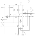
도 8은 본 발명의 일 실시예에 따른 화소(PXaij)의 회로도이다.Figure 8 is a circuit diagram of a pixel (PXaij) according to an embodiment of the present invention.
도 8에 도시된 화소(PXaij)는 도 2에 도시된 화소(PXij)와 유사한 회로 구성을 포함한다. 그러므로 도 2에 도시된 화소(PXij)와 동일한 구성 요소에 대해서는 동일한 인출 부호를 병기하고, 중복되는 설명을 생략한다.The pixel PXaij shown in FIG. 8 includes a circuit configuration similar to the pixel PXij shown in FIG. 2. Therefore, for the same components as the pixel PXij shown in FIG. 2, the same reference numerals are used, and overlapping descriptions are omitted.
도 8을 참조하면, 화소(PXaij)의 제7 트랜지스터(T7a)는 발광 소자(ED)의 애노드와 연결된 제1 전극, 제5 구동 전압 라인(VL5)과 연결된 제2 전극 및 스캔 라인(EBLi)과 연결된 게이트 전극을 포함한다. 제7 트랜지스터(T7)는 스캔 라인(EBLi)을 통해 전달받은 스캔 신호(EBi)에 따라 턴 온되어 발광 소자(ED)의 애노드를 제5 구동 전압 라인(VL5)의 제2 초기화 전압(VAINT)으로 초기화할 수 있다. 일 실시예에서, 제2 초기화 전압(VAINT)은 제1 초기화 전압(VINT)과 다른 전압 레벨을 가질 수 있다. 일 실시예에서, 제2 초기화 전압(VAINT)은 도 1에 도시된 전압 발생기(500)에 의해 생성될 수 있다.Referring to FIG. 8, the seventh transistor T7a of the pixel PXaij has a first electrode connected to the anode of the light emitting element ED, a second electrode connected to the fifth driving voltage line VL5, and a scan line EBLi. It includes a gate electrode connected to. The seventh transistor T7 is turned on according to the scan signal EBi received through the scan line EBLi to connect the anode of the light emitting device ED to the second initialization voltage VAINT of the fifth driving voltage line VL5. It can be initialized with . In one embodiment, the second initialization voltage VAINT may have a voltage level different from the first initialization voltage VINT. In one embodiment, the second initialization voltage VAINT may be generated by the
도 9는 본 발명의 일 실시예에 따른 화소(PXbij)의 회로도이다.Figure 9 is a circuit diagram of a pixel (PXbij) according to an embodiment of the present invention.
도 9에 도시된 화소(PXbij)는 도 2에 도시된 화소(PXij)와 유사한 회로 구성을 포함한다. 그러므로 도 2에 도시된 화소(PXij)와 동일한 구성 요소에 대해서는 동일한 인출 부호를 병기하고, 중복되는 설명을 생략한다.The pixel PXbij shown in FIG. 9 includes a circuit configuration similar to the pixel PXij shown in FIG. 2. Therefore, for the same components as the pixel PXij shown in FIG. 2, the same reference numerals are used, and overlapping descriptions are omitted.
도 9를 참조하면, 화소(PXbij)의 제5 트랜지스터(T5a)는 제6 구동 전압 라인(VL6)과 연결된 제1 전극, 제2 노드(N2)와 연결된 제2 전극 및 스캔 라인(GCLi)에 연결된 게이트 전극을 포함한다. 제5 트랜지스터(T5a)는 스캔 라인(GCLi)을 통해 전달받은 스캔 신호(GCi)에 따라 턴 온되어 제6 구동 전압 라인(VL6)의 기준 전압(VREF)을 제2 노드(N2)에 전달할 수 있다.Referring to FIG. 9, the fifth transistor T5a of the pixel PXbij is connected to the first electrode connected to the sixth driving voltage line VL6, the second electrode connected to the second node N2, and the scan line GCLi. It includes a connected gate electrode. The fifth transistor T5a is turned on according to the scan signal GCi received through the scan line GCLi and can transmit the reference voltage VREF of the sixth driving voltage line VL6 to the second node N2. there is.
도 10은 본 발명의 일 실시예에 따른 화소(PXcij)의 회로도이다.Figure 10 is a circuit diagram of a pixel (PXcij) according to an embodiment of the present invention.
도 10에 도시된 화소(PXcij)는 도 2에 도시된 화소(PXij)와 유사한 회로 구성을 포함한다. 그러므로 도 2에 도시된 화소(PXij)와 동일한 구성 요소에 대해서는 동일한 인출 부호를 병기하고, 중복되는 설명을 생략한다.The pixel PXcij shown in FIG. 10 includes a circuit configuration similar to the pixel PXij shown in FIG. 2. Therefore, for the same components as the pixel PXij shown in FIG. 2, the same reference numerals are used, and overlapping descriptions are omitted.
도 10을 참조하면, 화소(PXcij)의 제7 트랜지스터(T7a)는 발광 소자(ED)의 애노드와 연결된 제1 전극, 제5 구동 전압 라인(VL5)과 연결된 제2 전극 및 스캔 라인(EBLi)과 연결된 게이트 전극을 포함한다. 제7 트랜지스터(T7)는 스캔 라인(EBLi)을 통해 전달받은 스캔 신호(EBi)에 따라 턴 온되어 발광 소자(ED)의 애노드를 제5 구동 전압 라인(VL5)의 제2 초기화 전압(VAINT)으로 초기화할 수 있다. 일 실시예에서, 제2 초기화 전압(VAINT)은 제1 초기화 전압(VINT)과 다른 전압 레벨을 가질 수 있다.Referring to FIG. 10, the seventh transistor T7a of the pixel PXcij has a first electrode connected to the anode of the light emitting element ED, a second electrode connected to the fifth driving voltage line VL5, and a scan line EBLi. It includes a gate electrode connected to. The seventh transistor T7 is turned on according to the scan signal EBi received through the scan line EBLi to connect the anode of the light emitting device ED to the second initialization voltage VAINT of the fifth driving voltage line VL5. It can be initialized with . In one embodiment, the second initialization voltage VAINT may have a voltage level different from the first initialization voltage VINT.
화소(PXcij)의 제5 트랜지스터(T5a)는 제6 구동 전압 라인(VL6)과 연결된 제1 전극, 제2 노드(N2)와 연결된 제2 전극 및 스캔 라인(GCLi)에 연결된 게이트 전극을 포함한다. 제5 트랜지스터(T5)는 스캔 라인(GCLi)을 통해 전달받은 스캔 신호(GCi)에 따라 턴 온되어 제6 구동 전압 라인(VL6)의 기준 전압(VREF)을 제2 노드(N2)에 전달할 수 있다.The fifth transistor T5a of the pixel PXcij includes a first electrode connected to the sixth driving voltage line VL6, a second electrode connected to the second node N2, and a gate electrode connected to the scan line GCLi. . The fifth transistor T5 is turned on according to the scan signal GCi received through the scan line GCLi and can transmit the reference voltage VREF of the sixth driving voltage line VL6 to the second node N2. there is.
도 4a에 도시된 제4 구간(P4)에서 스캔 신호(GCi)가 활성 레벨이면, 턴 온 상태의 제5 트랜지스터(T5)를 통해 기준 전압(VREF)이 제2 노드(N2)로 전달된다.If the scan signal GCi is at an active level in the fourth section P4 shown in FIG. 4A, the reference voltage VREF is transmitted to the second node N2 through the fifth transistor T5 in the turned-on state.
제5 구간(P5)에서 제2 노드(N2)의 전압은 기준 전압(VREF)에서 데이터 신호(Dj)의 전압(Vdata)으로 변경된다. 제2 노드(N2)의 전압 변화량 "Vdata-Vref"가 제1 커패시터(Cst)의 커플링에 의해 제1 노드(N1)로 전달될 수 있다.In the fifth section P5, the voltage of the second node N2 changes from the reference voltage VREF to the voltage Vdata of the data signal Dj. The voltage change “Vdata-Vref” of the second node N2 may be transmitted to the first node N1 through coupling of the first capacitor Cst.
제4 구간(P4)에서 제1 노드(N1)의 전압은 "ELVDD-Vth"이었으므로, 제5 구간(P5)에서 제1 노드(N1) 즉, 제1 트랜지스터(T1)의 게이트 전극의 전압은 "ELVDD-Vth + (Vdata- Vref)"으로 된다.Since the voltage of the first node (N1) in the fourth section (P4) was “ELVDD-Vth”, the voltage of the first node (N1), that is, the gate electrode of the first transistor (T1) in the fifth section (P5) It becomes “ELVDD-Vth + (Vdata- Vref)”.
제7 구간(P7)에서 제1 트랜지스터(T1)를 통해 흐르는 전류는 제1 트랜지스터(T1)의 제1 전극과 게이트 전극 간의 전압 차(Vgs)와 제1 트랜지스터(T1)의 스레숄드 전압(Vth)의 차의 제곱 "(Vgs-Vth)2"에 비례한다.The current flowing through the first transistor (T1) in the seventh section (P7) is the voltage difference (Vgs) between the first electrode and the gate electrode of the first transistor (T1) and the threshold voltage (Vth) of the first transistor (T1) The square of the difference is proportional to "(Vgs-Vth) 2 ".
제1 트랜지스터(T1)의 제1 전극의 전압은 제1 구동 전압(ELVDD)이고, 제1 트랜지스터(T1)의 게이트 전극의 전압은 "ELVDD-Vth+(Vdata-Vref)"이므로 제1 트랜지스터(T1)의 제1 전극과 게이트 전극 간의 전압 차(Vgs)는 "ELVDD-(ELVDD-Vth+(Vdata- Vref))"이다.The voltage of the first electrode of the first transistor T1 is the first driving voltage ELVDD, and the voltage of the gate electrode of the first transistor T1 is “ELVDD-Vth+(Vdata-Vref)”, so the first transistor T1 ) The voltage difference (Vgs) between the first electrode and the gate electrode is “ELVDD-(ELVDD-Vth+(Vdata-Vref))”.
그러므로 제1 트랜지스터(T1)를 통해 흐르는 전류는 "(ELVDD-(ELVDD-Vth+(Vdata-Vref)-Vth))2"에 비례한다. 즉, 제1 트랜지스터(T1)를 통해 흐르는 전류는 "(Vref -Vdata)2"에 비례한다.Therefore, the current flowing through the first transistor T1 is proportional to "(ELVDD-(ELVDD-Vth+(Vdata-Vref)-Vth)) 2 ". That is, the current flowing through the first transistor T1 is proportional to "(Vref -Vdata) 2 ".
따라서 제1 트랜지스터(T1)의 스레숄드 전압(Vth)의 영향을 제거하고, 데이터 신호(Dj)의 전압(Vata)에 비례하는 전류가 발광 소자(ED)로 제공될 수 있다. 제7 구간(P7)은 발광 소자(ED)가 발광하는 발광 구간일 수 있다.Accordingly, the influence of the threshold voltage (Vth) of the first transistor (T1) can be removed, and a current proportional to the voltage (Vata) of the data signal (Dj) can be provided to the light emitting device (ED). The seventh section P7 may be a light-emitting section in which the light-emitting device ED emits light.
도 11은 본 발명의 일 실시예에 따른 화소(PXdij)의 회로도이다.Figure 11 is a circuit diagram of a pixel (PXdij) according to an embodiment of the present invention.
도 11에 도시된 화소(PXdij)는 도 2에 도시된 화소(PXij)와 유사한 회로 구성을 포함한다. 그러므로 도 2에 도시된 화소(PXij)와 동일한 구성 요소에 대해서는 동일한 인출 부호를 병기하고, 중복되는 설명을 생략한다.The pixel PXdij shown in FIG. 11 includes a circuit configuration similar to the pixel PXij shown in FIG. 2. Therefore, for the same components as the pixel PXij shown in FIG. 2, the same reference numerals are used, and overlapping descriptions are omitted.
도 11을 참조하면, 화소(PXdij)의 제5 트랜지스터(T5b)는 제10 트랜지스터(T10)의 제2 전극과 연결된 제1 전극, 제2 노드(N2)와 연결된 제2 전극 및 스캔 라인(GCLi)에 연결된 게이트 전극을 포함한다. 제5 트랜지스터(T5b)는 스캔 라인(GCLi)을 통해 전달받은 스캔 신호(GCi)에 따라 턴 온되어 제10 트랜지스터(T10)의 제2 전극을 제2 노드(N2)에 연결한다.Referring to FIG. 11, the fifth transistor T5b of the pixel PXdij has a first electrode connected to the second electrode of the tenth transistor T10, a second electrode connected to the second node N2, and a scan line GCLi. ) includes a gate electrode connected to The fifth transistor T5b is turned on according to the scan signal GCi received through the scan line GCLi and connects the second electrode of the tenth transistor T10 to the second node N2.
제5 트랜지스터(T5b)의 게이트 전극 및 제10 트랜지스터(T10)의 게이트 전극이 모두 스캔 라인(GCLi)에 연결되어 있으므로, 제5 트랜지스터(T5b) 및 제10 트랜지스터(T10)는 스캔 신호(GCi)에 따라 동시에 턴 온될 수 있다. 도 4a에 도시된 제2 구간(P2) 및 제4 구간(P4) 각각에서 활성 레벨의 스캔 신호(GCi)에 응답해서 제10 트랜지스터(T10) 및 제5 트랜지스터(T5b)가 턴 온되면 제1 구동 전압(ELVDD)이 제10 트랜지스터(T10) 및 제5 트랜지스터(T5b)를 통해 제2 노드(N2)로 전달될 수 있다.Since both the gate electrode of the fifth transistor (T5b) and the gate electrode of the tenth transistor (T10) are connected to the scan line (GCLi), the fifth transistor (T5b) and the tenth transistor (T10) are connected to the scan signal (GCi) Depending on, they may be turned on at the same time. When the tenth transistor T10 and the fifth transistor T5b are turned on in response to the scan signal GCi at the active level in each of the second period P2 and the fourth period P4 shown in FIG. 4A, the first transistor T10 and T5b are turned on. The driving voltage ELVDD may be transmitted to the second node N2 through the tenth transistor T10 and the fifth transistor T5b.
한편, 제2 구간(P2) 및 제4 구간(P4) 각각에서 스캔 신호(GCi)가 활성 레벨이면, 제3 트랜지스터(T3)도 턴 온될 수 있다. 제3 트랜지스터(T3) 및 제10 트랜지스터(T10)가 턴 온 됨에 따라 제10 트랜지스터(T10), 제1 트랜지스터(T1) 및 제3 트랜지스터(T3)를 통해 제1 구동 전압(ELVDD)이 제1 노드(N1)로 전달될 수 있다.Meanwhile, when the scan signal GCi is at an active level in each of the second period P2 and the fourth period P4, the third transistor T3 may also be turned on. As the third transistor T3 and the tenth transistor T10 are turned on, the first driving voltage ELVDD becomes the first through the tenth transistor T10, the first transistor T1, and the third transistor T3. It can be transmitted to node N1.
도 12는 본 발명의 일 실시예에 따른 화소(PXeij)의 회로도이다.Figure 12 is a circuit diagram of a pixel (PXeij) according to an embodiment of the present invention.
도 12에 도시된 화소(PXeij)는 도 2에 도시된 화소(PXij)와 유사한 회로 구성을 포함한다. 그러므로 도 2에 도시된 화소(PXij)와 동일한 구성 요소에 대해서는 동일한 인출 부호를 병기하고, 중복되는 설명을 생략한다.The pixel PXeij shown in FIG. 12 includes a circuit configuration similar to the pixel PXij shown in FIG. 2. Therefore, for the same components as the pixel PXij shown in FIG. 2, the same reference numerals are used, and overlapping descriptions are omitted.
도 12를 참조하면, 화소(PXeij)의 제5 트랜지스터(T5b)는 제10 트랜지스터(T10)의 제2 전극과 연결된 제1 전극, 제2 노드(N2)와 연결된 제2 전극 및 스캔 라인(GCLi)에 연결된 게이트 전극을 포함한다. 제5 트랜지스터(T5b)는 스캔 라인(GCLi)을 통해 전달받은 스캔 신호(GCi)에 따라 턴 온되어 제10 트랜지스터(T10)의 제2 전극을 제2 노드(N2)에 연결한다.Referring to FIG. 12, the fifth transistor T5b of the pixel PXeij has a first electrode connected to the second electrode of the tenth transistor T10, a second electrode connected to the second node N2, and a scan line GCLi. ) includes a gate electrode connected to The fifth transistor T5b is turned on according to the scan signal GCi received through the scan line GCLi and connects the second electrode of the tenth transistor T10 to the second node N2.
화소(PXeij)의 제7 트랜지스터(T7a)는 발광 소자(ED)의 애노드와 연결된 제1 전극, 제5 구동 전압 라인(VL5)과 연결된 제2 전극 및 스캔 라인(EBLi)과 연결된 게이트 전극을 포함한다. 제7 트랜지스터(T7)는 스캔 라인(EBLi)을 통해 전달받은 스캔 신호(EBi)에 따라 턴 온되어 발광 소자(ED)의 애노드를 제5 구동 전압 라인(VL5)의 제2 초기화 전압(VAINT)으로 초기화할 수 있다. 일 실시예에서, 제2 초기화 전압(VAINT)은 제1 초기화 전압(VINT)과 다른 전압 레벨을 가질 수 있다. 일 실시예에서, 제2 초기화 전압(VAINT)은 도 1에 도시된 전압 발생기(500)에 의해 생성될 수 있다.The seventh transistor T7a of the pixel PXeij includes a first electrode connected to the anode of the light emitting element ED, a second electrode connected to the fifth driving voltage line VL5, and a gate electrode connected to the scan line EBLi. do. The seventh transistor T7 is turned on according to the scan signal EBi received through the scan line EBLi to connect the anode of the light emitting device ED to the second initialization voltage VAINT of the fifth driving voltage line VL5. It can be initialized with . In one embodiment, the second initialization voltage VAINT may have a voltage level different from the first initialization voltage VINT. In one embodiment, the second initialization voltage VAINT may be generated by the
이상에서는 본 발명의 바람직한 실시예를 참조하여 설명하였지만, 해당 기술 분야의 숙련된 당업자 또는 해당 기술 분야에 통상의 지식을 갖는 자라면, 후술될 특허청구범위에 기재된 본 발명의 사상 및 기술 영역으로부터 벗어나지 않는 범위 내에서 본 발명을 다양하게 수정 및 변경시킬 수 있음을 이해할 수 있을 것이다. 따라서, 본 발명의 기술적 범위는 명세서의 상세한 설명에 기재된 내용으로 한정되는 것이 아니라 특허청구범위에 의해 정해져야만 할 것이다.Although the present invention has been described above with reference to preferred embodiments, those skilled in the art or have ordinary knowledge in the relevant technical field should not deviate from the spirit and technical scope of the present invention as set forth in the claims to be described later. It will be understood that the present invention can be modified and changed in various ways within the scope not permitted. Therefore, the technical scope of the present invention should not be limited to what is described in the detailed description of the specification, but should be determined by the scope of the patent claims.
DD: 표시 장치
DP: 표시 패널
100: 구동 컨트롤러
200: 데이터 구동 회로
300: 제1 구동 회로
400: 제2 구동 회로
500: 전압 발생기DD: display device
DP: Display panel
100: Drive controller
200: data driving circuit
300: first driving circuit
400: second driving circuit
500: voltage generator
Claims (23)
제1 전극, 제2 전극 및 제1 노드와 연결된 게이트 전극을 포함하는 제1 트랜지스터;
상기 제1 노드와 제2 노드 사이에 연결된 제1 커패시터;
상기 제1 트랜지스터의 상기 제2 전극과 상기 제1 노드 사이에 연결되고, 제1 스캔 라인과 연결된 게이트 전극을 포함하는 제2 트랜지스터;
제1 전극, 상기 제1 노드와 연결된 제2 전극 및 상기 제1 스캔 라인과 연결된 게이트 전극을 포함하는 제3 트랜지스터; 및
제1 구동 전압 라인과 연결된 제1 전극, 상기 제1 트랜지스터의 상기 제1 전극과 연결된 제2 전극 및 상기 제1 스캔 라인과 연결된 게이트 전극을 포함하는 제4 트랜지스터를 포함하는 화소.A light emitting device including an anode and a cathode;
A first transistor including a first electrode, a second electrode, and a gate electrode connected to the first node;
a first capacitor connected between the first node and the second node;
a second transistor connected between the second electrode of the first transistor and the first node and including a gate electrode connected to a first scan line;
a third transistor including a first electrode, a second electrode connected to the first node, and a gate electrode connected to the first scan line; and
A pixel including a fourth transistor including a first electrode connected to a first driving voltage line, a second electrode connected to the first electrode of the first transistor, and a gate electrode connected to the first scan line.
보상 구간동안 상기 제1 스캔 라인으로 제공되는 제1 스캔 신호가 활성 레벨일 때 상기 제1 구동 전압 라인으로부터의 제1 구동 전압이 상기 제4 트랜지스터, 상기 제1 트랜지스터 및 상기 제2 트랜지스터를 통해 상기 제1 노드로 전달되는 화소.According to claim 1,
During the compensation period, when the first scan signal provided to the first scan line is at an active level, the first driving voltage from the first driving voltage line is transmitted through the fourth transistor, the first transistor, and the second transistor. Pixel delivered to the first node.
상기 제3 트랜지스터의 상기 제1 전극은 상기 제1 구동 전압 라인과 연결되고,
상기 보상 구간동안 상기 제1 스캔 신호가 활성 레벨일 때 상기 제1 구동 전압 라인으로부터의 제1 구동 전압이 상기 제3 트랜지스터를 통해 상기 제2 노드로 전달되는 화소.According to claim 2,
The first electrode of the third transistor is connected to the first driving voltage line,
A pixel in which a first driving voltage from the first driving voltage line is transmitted to the second node through the third transistor when the first scan signal is at an active level during the compensation period.
상기 제1 노드와 제2 구동 전압 라인 사이에 연결되고, 제2 스캔 라인과 연결된 게이트 전극을 포함하는 제5 트랜지스터를 더 포함하되,
초기화 구간동안 상기 제2 스캔 라인으로 제공되는 제2 스캔 신호가 활성 레벨일 때 상기 제2 구동 전압 라인으로부터의 제2 구동 전압이 상기 제5 트랜지스터를 통해 상기 제1 노드로 전달되는 화소.According to claim 3,
It further includes a fifth transistor connected between the first node and the second driving voltage line and including a gate electrode connected to the second scan line,
A pixel in which a second driving voltage from the second driving voltage line is transmitted to the first node through the fifth transistor when a second scan signal provided to the second scan line is at an active level during an initialization period.
상기 초기화 구간 및 상기 보상 구간은 번갈아 복수 회 반복되는 화소.According to claim 4,
A pixel in which the initialization section and the compensation section are alternately repeated multiple times.
상기 제2 구동 전압 라인과 상기 발광 소자의 상기 애노드 사이에 연결되고, 제3 스캔 라인과 연결된 게이트 전극을 포함하는 제6 트랜지스터; 및
제3 구동 전압 라인과 상기 제1 트랜지스터의 상기 제1 전극 사이에 연결되고, 상기 제3 스캔 라인과 연결된 게이트 전극을 포함하는 제7 트랜지스터를 더 포함하는 화소.According to claim 4,
a sixth transistor connected between the second driving voltage line and the anode of the light emitting device and including a gate electrode connected to a third scan line; and
The pixel further includes a seventh transistor connected between a third driving voltage line and the first electrode of the first transistor and including a gate electrode connected to the third scan line.
제1 구동 전압 라인과 상기 제1 트랜지스터의 상기 제1 전극 사이에 연결되고, 발광 라인과 연결된 게이트 전극을 포함하는 제8 트랜지스터; 및
상기 제1 트랜지스터의 상기 제2 전극과 상기 발광 소자의 상기 애노드 사이에 연결되고, 상기 발광 라인과 연결된 게이트 전극을 포함하는 제9 트랜지스터를 더 포함하는 화소.According to claim 1,
an eighth transistor connected between a first driving voltage line and the first electrode of the first transistor and including a gate electrode connected to a light emitting line; and
The pixel further includes a ninth transistor connected between the second electrode of the first transistor and the anode of the light-emitting device and including a gate electrode connected to the light-emitting line.
데이터 라인과 상기 제2 노드 사이에 연결되고, 제4 스캔 라인과 연결된 게이트 전극을 포함하는 제10 트랜지스터를 더 포함하는 화소.According to claim 1,
A pixel further comprising a tenth transistor connected between a data line and the second node and including a gate electrode connected to a fourth scan line.
제4 구동 전압 라인과 상기 발광 소자의 상기 애노드 사이에 연결되고, 제3 스캔 라인과 연결된 게이트 전극을 포함하는 제11 트랜지스터; 및
제3 구동 전압 라인과 상기 제1 트랜지스터의 상기 제1 전극 사이에 연결되고, 상기 제3 스캔 라인과 연결된 게이트 전극을 포함하는 제12 트랜지스터를 더 포함하는 화소.According to claim 1,
an eleventh transistor connected between a fourth driving voltage line and the anode of the light emitting device and including a gate electrode connected to a third scan line; and
The pixel further includes a twelfth transistor connected between a third driving voltage line and the first electrode of the first transistor and including a gate electrode connected to the third scan line.
상기 제3 트랜지스터의 상기 제1 전극은 기준 전압을 수신하는 제5 전압 라인과 연결되는 화소.According to claim 1,
The first electrode of the third transistor is connected to a fifth voltage line that receives a reference voltage.
제4 구동 전압 라인과 상기 발광 소자의 상기 애노드 사이에 연결되고, 제3 스캔 라인과 연결된 게이트 전극을 포함하는 제13 트랜지스터; 및
제3 구동 전압 라인과 상기 제1 트랜지스터의 상기 제1 전극 사이에 연결되고, 상기 제3 스캔 라인과 연결된 게이트 전극을 포함하는 제14 트랜지스터를 더 포함하는 화소.According to claim 10,
a thirteenth transistor connected between a fourth driving voltage line and the anode of the light emitting device and including a gate electrode connected to a third scan line; and
The pixel further includes a fourteenth transistor connected between a third driving voltage line and the first electrode of the first transistor and including a gate electrode connected to the third scan line.
상기 제3 트랜지스터의 상기 제1 전극은 상기 제4 트랜지스터의 상기 제2 전극과 연결되는 화소.According to claim 1,
A pixel in which the first electrode of the third transistor is connected to the second electrode of the fourth transistor.
제4 구동 전압 라인과 상기 발광 소자의 상기 애노드 사이에 연결되고, 제3 스캔 라인과 연결된 게이트 전극을 포함하는 제15 트랜지스터; 및
제3 구동 전압 라인과 상기 제1 트랜지스터의 상기 제1 전극 사이에 연결되고, 상기 제3 스캔 라인과 연결된 게이트 전극을 포함하는 제16 트랜지스터를 더 포함하는 화소. According to claim 12,
a fifteenth transistor connected between a fourth driving voltage line and the anode of the light emitting device and including a gate electrode connected to a third scan line; and
The pixel further includes a 16th transistor connected between a third driving voltage line and the first electrode of the first transistor and including a gate electrode connected to the third scan line.
스캔 제어 신호에 응답해서 상기 복수의 스캔 라인들 및 상기 발광 라인을 구동하는 구동 회로;
상기 스캔 제어 신호를 출력하는 구동 컨트롤러; 및
복수의 구동 전압들을 발생하는 전압 발생기를 포함하되,
상기 화소는,
애노드 및 캐소드를 포함하는 발광 소자;
제1 전극, 제2 전극 및 제1 노드와 연결된 게이트 전극을 포함하는 제1 트랜지스터;
상기 제1 노드와 제2 노드 사이에 연결된 제1 커패시터;
상기 제1 트랜지스터의 상기 제2 전극과 상기 제1 노드 사이에 연결되고, 상기 복수의 스캔 라인들 중 제1 스캔 라인과 연결된 게이트 전극을 포함하는 제2 트랜지스터;
제1 전극, 상기 제1 노드와 연결된 제2 전극 및 상기 제1 스캔 라인과 연결된 게이트 전극을 포함하는 제3 트랜지스터; 및
상기 복수의 구동 전압들 중 제1 구동 전압을 전달하는 제1 구동 전압 라인과 연결된 제1 전극, 상기 제1 트랜지스터의 상기 제1 전극과 연결된 제2 전극 및 상기 제1 스캔 라인과 연결된 게이트 전극을 포함하는 제4 트랜지스터를 포함하되,
상기 제1 스캔 라인으로 제공되는 제1 스캔 신호가 활성 레벨일 때 상기 제1 구동 전압이 상기 제4 트랜지스터, 상기 제1 트랜지스터 및 상기 제2 트랜지스터를 통해 상기 제1 노드로 전달되는 표시 장치.A display panel including a pixel connected to a plurality of scan lines, a light emission line, and a data line;
a driving circuit that drives the plurality of scan lines and the light emitting line in response to a scan control signal;
a driving controller outputting the scan control signal; and
Including a voltage generator that generates a plurality of driving voltages,
The pixel is,
A light emitting device including an anode and a cathode;
A first transistor including a first electrode, a second electrode, and a gate electrode connected to the first node;
a first capacitor connected between the first node and the second node;
a second transistor connected between the second electrode of the first transistor and the first node and including a gate electrode connected to a first scan line among the plurality of scan lines;
a third transistor including a first electrode, a second electrode connected to the first node, and a gate electrode connected to the first scan line; and
A first electrode connected to a first driving voltage line that transmits a first driving voltage among the plurality of driving voltages, a second electrode connected to the first electrode of the first transistor, and a gate electrode connected to the first scan line. A fourth transistor comprising:
A display device in which the first driving voltage is transmitted to the first node through the fourth transistor, the first transistor, and the second transistor when the first scan signal provided to the first scan line is at an active level.
상기 제3 트랜지스터의 상기 제1 전극은 상기 제1 구동 전압 라인과 연결되고,
상기 제1 스캔 신호가 활성 레벨일 때 상기 제1 구동 전압이 상기 제3 트랜지스터를 통해 상기 제2 노드로 전달되는 표시 장치. According to claim 14,
The first electrode of the third transistor is connected to the first driving voltage line,
A display device in which the first driving voltage is transmitted to the second node through the third transistor when the first scan signal is at an active level.
상기 화소는,
제1 구동 전압 라인과 상기 제1 트랜지스터의 상기 제1 전극 사이에 연결되고, 상기 발광 신호를 전달하는 발광 라인과 연결된 게이트 전극을 포함하는 제5 트랜지스터; 및
상기 제1 트랜지스터의 상기 제2 전극과 상기 발광 소자의 상기 애노드 사이에 연결되고, 상기 발광 라인과 연결된 게이트 전극을 포함하는 제6 트랜지스터를 더 포함하는 표시 장치.According to claim 14,
The pixel is,
a fifth transistor connected between a first driving voltage line and the first electrode of the first transistor and including a gate electrode connected to the light emitting line transmitting the light emitting signal; and
The display device further includes a sixth transistor connected between the second electrode of the first transistor and the anode of the light emitting device and including a gate electrode connected to the light emitting line.
상기 제3 트랜지스터의 상기 제1 전극은 상기 제4 트랜지스터의 상기 제2 전극과 연결되는 표시 장치.According to claim 14,
The display device wherein the first electrode of the third transistor is connected to the second electrode of the fourth transistor.
상기 화소는,
데이터 라인과 상기 제2 노드 사이에 연결되고, 상기 복수의 스캔 라인들 중 제2 스캔 라인과 연결된 게이트 전극을 포함하는 제7 트랜지스터;
상기 제1 노드와 제2 구동 전압 라인 사이에 연결되고, 상기 복수의 스캔 라인들 중 제3 스캔 라인과 연결된 게이트 전극을 포함하는 제8 트랜지스터;
상기 제2 구동 전압 라인과 상기 발광 소자의 상기 애노드 사이에 연결되고, 상기 복수의 스캔 라인들 중 제4 스캔 라인과 연결된 게이트 전극을 포함하는 제9 트랜지스터; 및
제3 구동 전압 라인과 상기 제1 트랜지스터의 상기 제1 전극 사이에 연결되고, 상기 제4 스캔 라인과 연결된 게이트 전극을 포함하는 제10 트랜지스터를 더 포함하는 표시 장치.According to claim 14,
The pixel is,
a seventh transistor connected between a data line and the second node and including a gate electrode connected to a second scan line among the plurality of scan lines;
an eighth transistor connected between the first node and a second driving voltage line and including a gate electrode connected to a third scan line among the plurality of scan lines;
a ninth transistor connected between the second driving voltage line and the anode of the light emitting device and including a gate electrode connected to a fourth scan line among the plurality of scan lines; and
The display device further includes a tenth transistor connected between a third driving voltage line and the first electrode of the first transistor and including a gate electrode connected to the fourth scan line.
상기 스캔 제어 신호에 응답해서 상기 발광 신호를 출력하는 발광 구동 회로;
상기 스캔 제어 신호에 응답해서 상기 제1 스캔 신호를 출력하는 제1 스캔 구동 회로;
상기 스캔 제어 신호에 응답해서 상기 제2 스캔 신호 및 상기 제3 스캔 신호를 출력하는 제2 스캔 구동 회로; 및
상기 스캔 제어 신호에 응답해서 상기 제4 스캔 신호를 출력하는 제3 스캔 구동 회로를 포함하는 표시 장치. According to claim 18,
a light emission driving circuit that outputs the light emission signal in response to the scan control signal;
a first scan driving circuit that outputs the first scan signal in response to the scan control signal;
a second scan driving circuit that outputs the second scan signal and the third scan signal in response to the scan control signal; and
A display device comprising a third scan driving circuit that outputs the fourth scan signal in response to the scan control signal.
초기화 전압이 상기 제1 노드로 전달되도록 제1 스캔 신호를 활성 레벨로 출력하는 초기화 단계; 및
제1 구동 전압이 상기 제1 노드 및 상기 제2 노드로 각각 전달되도록 제2 스캔 신호를 활성 레벨로 출력하는 보상 단계를 포함하고;
상기 보상 단계에서 상기 제1 구동 전압을 전달하는 제1 구동 전압 라인과 연결된 제1 전극, 상기 제1 트랜지스터의 상기 제1 전극과 연결된 제2 전극 및 상기 제1 스캔 신호를 수신하는 게이트 전극을 포함하는 제2 트랜지스터가 턴 온되는 화소의 구동 방법.In a method of driving a pixel including a first transistor including a first electrode, a second electrode connected to the first node, and a gate electrode, and a capacitor connected between the first node and the second node:
An initialization step of outputting a first scan signal at an active level so that an initialization voltage is transmitted to the first node; and
A compensation step of outputting a second scan signal at an active level so that a first driving voltage is transmitted to the first node and the second node, respectively;
In the compensation step, it includes a first electrode connected to a first driving voltage line that transmits the first driving voltage, a second electrode connected to the first electrode of the first transistor, and a gate electrode that receives the first scan signal. A method of driving a pixel in which the second transistor is turned on.
상기 보상 단계에서 상기 제1 구동 전압 라인과 상기 제2 노드 사이에 연결된 제3 트랜지스터가 턴 온되는 화소의 구동 방법.According to claim 20,
A method of driving a pixel in which a third transistor connected between the first driving voltage line and the second node is turned on in the compensation step.
상기 보상 단계에서 상기 제2 트랜지스터의 상기 제2 전극과 상기 제2 노드 사이에 연결된 제4 트랜지스터가 턴 온되는 화소의 구동 방법.According to claim 20,
A method of driving a pixel in which a fourth transistor connected between the second electrode and the second node of the second transistor is turned on in the compensation step.
상기 보상 단계에서 기준 전압을 전달하는 제2 구동 전압 라인과 상기 제2 노드 사이에 연결된 제5 트랜지스터가 턴 온되는 화소의 구동 방법.According to claim 20,
A method of driving a pixel in which a fifth transistor connected between a second driving voltage line transmitting a reference voltage and the second node is turned on in the compensation step.
Priority Applications (6)
| Application Number | Priority Date | Filing Date | Title |
|---|---|---|---|
| KR1020220111180A KR20240033711A (en) | 2022-09-02 | 2022-09-02 | Pixel and display device |
| US18/196,137 US11961463B2 (en) | 2022-09-02 | 2023-05-11 | Pixel and display device |
| EP23194132.9A EP4332952A1 (en) | 2022-09-02 | 2023-08-30 | Pixel and display device |
| CN202311116817.0A CN117649822A (en) | 2022-09-02 | 2023-09-01 | Pixel, display device and driving method of pixel |
| US18/597,393 US12322328B2 (en) | 2022-09-02 | 2024-03-06 | Pixel and display device capable of operating at high operating frequency |
| US19/219,132 US20250285583A1 (en) | 2022-09-02 | 2025-05-27 | Pixel and display device |
Applications Claiming Priority (1)
| Application Number | Priority Date | Filing Date | Title |
|---|---|---|---|
| KR1020220111180A KR20240033711A (en) | 2022-09-02 | 2022-09-02 | Pixel and display device |
Publications (1)
| Publication Number | Publication Date |
|---|---|
| KR20240033711A true KR20240033711A (en) | 2024-03-13 |
Family
ID=87863425
Family Applications (1)
| Application Number | Title | Priority Date | Filing Date |
|---|---|---|---|
| KR1020220111180A Pending KR20240033711A (en) | 2022-09-02 | 2022-09-02 | Pixel and display device |
Country Status (4)
| Country | Link |
|---|---|
| US (3) | US11961463B2 (en) |
| EP (1) | EP4332952A1 (en) |
| KR (1) | KR20240033711A (en) |
| CN (1) | CN117649822A (en) |
Cited By (3)
| Publication number | Priority date | Publication date | Assignee | Title |
|---|---|---|---|---|
| US12499837B2 (en) | 2024-01-16 | 2025-12-16 | Samsung Display Co., Ltd. | Display apparatus and method of driving the same |
| US12542111B2 (en) | 2024-07-08 | 2026-02-03 | Samsung Display Co., Ltd. | Display device and electronic device including the same |
| US12609082B2 (en) | 2023-11-23 | 2026-04-21 | Samsung Display Co., Ltd. | Pixel and display device including the same |
Families Citing this family (2)
| Publication number | Priority date | Publication date | Assignee | Title |
|---|---|---|---|---|
| JP2013093565A (en) * | 2011-10-07 | 2013-05-16 | Semiconductor Energy Lab Co Ltd | Semiconductor device |
| CN121600859A (en) * | 2024-08-14 | 2026-03-03 | 上海和辉光电股份有限公司 | Pixel driving circuit and display panel |
Family Cites Families (14)
| Publication number | Priority date | Publication date | Assignee | Title |
|---|---|---|---|---|
| KR101162864B1 (en) * | 2010-07-19 | 2012-07-04 | 삼성모바일디스플레이주식회사 | Pixel and Organic Light Emitting Display Device Using the same |
| KR102190161B1 (en) * | 2014-06-23 | 2020-12-14 | 삼성디스플레이 주식회사 | Pixel, display panel and organic light emitting display including the same |
| KR102309599B1 (en) * | 2017-04-11 | 2021-10-08 | 삼성디스플레이 주식회사 | Organic light emitting display device |
| KR102462008B1 (en) * | 2017-09-22 | 2022-11-03 | 삼성디스플레이 주식회사 | Organic light emitting display device |
| KR102527847B1 (en) * | 2018-06-18 | 2023-05-03 | 삼성디스플레이 주식회사 | Display apparatus |
| KR102501659B1 (en) * | 2018-10-02 | 2023-02-21 | 삼성디스플레이 주식회사 | Flicker quantification system and method of driving the same |
| JP2020154230A (en) * | 2019-03-22 | 2020-09-24 | 株式会社Jvcケンウッド | Liquid crystal display device and its manufacturing method |
| KR102665185B1 (en) | 2019-06-12 | 2024-05-16 | 삼성디스플레이 주식회사 | Display device |
| KR102591507B1 (en) * | 2019-07-22 | 2023-10-23 | 삼성디스플레이 주식회사 | Pixel and display device having the same |
| KR102657133B1 (en) * | 2019-07-22 | 2024-04-16 | 삼성디스플레이 주식회사 | Pixel and display device having the same |
| KR102764928B1 (en) * | 2019-07-26 | 2025-02-12 | 삼성디스플레이 주식회사 | Display device |
| KR102668850B1 (en) | 2019-08-12 | 2024-05-24 | 삼성디스플레이 주식회사 | Display device and method for driving the same |
| KR102756484B1 (en) | 2020-05-29 | 2025-01-21 | 삼성디스플레이 주식회사 | Display device |
| KR102775088B1 (en) | 2020-06-01 | 2025-03-05 | 삼성디스플레이 주식회사 | Display device |
-
2022
- 2022-09-02 KR KR1020220111180A patent/KR20240033711A/en active Pending
-
2023
- 2023-05-11 US US18/196,137 patent/US11961463B2/en active Active
- 2023-08-30 EP EP23194132.9A patent/EP4332952A1/en active Pending
- 2023-09-01 CN CN202311116817.0A patent/CN117649822A/en active Pending
-
2024
- 2024-03-06 US US18/597,393 patent/US12322328B2/en active Active
-
2025
- 2025-05-27 US US19/219,132 patent/US20250285583A1/en active Pending
Cited By (3)
| Publication number | Priority date | Publication date | Assignee | Title |
|---|---|---|---|---|
| US12609082B2 (en) | 2023-11-23 | 2026-04-21 | Samsung Display Co., Ltd. | Pixel and display device including the same |
| US12499837B2 (en) | 2024-01-16 | 2025-12-16 | Samsung Display Co., Ltd. | Display apparatus and method of driving the same |
| US12542111B2 (en) | 2024-07-08 | 2026-02-03 | Samsung Display Co., Ltd. | Display device and electronic device including the same |
Also Published As
| Publication number | Publication date |
|---|---|
| US20250285583A1 (en) | 2025-09-11 |
| CN117649822A (en) | 2024-03-05 |
| US20240212588A1 (en) | 2024-06-27 |
| US20240078963A1 (en) | 2024-03-07 |
| US11961463B2 (en) | 2024-04-16 |
| EP4332952A1 (en) | 2024-03-06 |
| US12322328B2 (en) | 2025-06-03 |
Similar Documents
| Publication | Publication Date | Title |
|---|---|---|
| CN113053281B (en) | Pixel driving circuit and electroluminescent display device including pixel driving circuit | |
| CN220189225U (en) | Pixel of display device | |
| CN111739468B (en) | Display apparatus | |
| KR20240033711A (en) | Pixel and display device | |
| CN114120919A (en) | Display device | |
| KR102950176B1 (en) | Display device | |
| KR102812881B1 (en) | Light emitting display apparatus | |
| KR20230056076A (en) | Display device and driving method thereof | |
| KR20230165953A (en) | Display device | |
| CN115223490A (en) | display device | |
| KR20240005264A (en) | Pixel, driver and display device having the same | |
| KR20230124160A (en) | Pixel and display device | |
| CN116364026A (en) | display device | |
| KR20230001618A (en) | Pixel and display device | |
| US20250225923A1 (en) | Pixel, display device including pixel, and pixel driving method | |
| CN117218999A (en) | display device | |
| KR20230102885A (en) | Light Emitting Display Device and Driving Method of the same | |
| KR101552991B1 (en) | Driving device of organic light emitting diode display device and driving method thereof | |
| CN120032583A (en) | Display device | |
| US12175921B2 (en) | Display device | |
| KR102872268B1 (en) | Driving controller, display device and method of driving the same | |
| CN115620673A (en) | Pixel and display device | |
| KR20230162837A (en) | Scan driver and display device having the same | |
| US11910662B2 (en) | Display device using a simultaneous light emitting method and driving method thereof | |
| KR20260062907A (en) | Display device |
Legal Events
| Date | Code | Title | Description |
|---|---|---|---|
| PA0109 | Patent application |
St.27 status event code: A-0-1-A10-A12-nap-PA0109 |
|
| PG1501 | Laying open of application |
St.27 status event code: A-1-1-Q10-Q12-nap-PG1501 |
|
| P11 | Amendment of application requested |
Free format text: ST27 STATUS EVENT CODE: A-2-2-P10-P11-NAP-X000 (AS PROVIDED BY THE NATIONAL OFFICE) |
|
| P11-X000 | Amendment of application requested |
St.27 status event code: A-2-2-P10-P11-nap-X000 |
|
| P13 | Application amended |
Free format text: ST27 STATUS EVENT CODE: A-2-2-P10-P13-NAP-X000 (AS PROVIDED BY THE NATIONAL OFFICE) |
|
| P13-X000 | Application amended |
St.27 status event code: A-2-2-P10-P13-nap-X000 |