KR102665185B1 - Display device - Google Patents
Display device Download PDFInfo
- Publication number
- KR102665185B1 KR102665185B1 KR1020190069638A KR20190069638A KR102665185B1 KR 102665185 B1 KR102665185 B1 KR 102665185B1 KR 1020190069638 A KR1020190069638 A KR 1020190069638A KR 20190069638 A KR20190069638 A KR 20190069638A KR 102665185 B1 KR102665185 B1 KR 102665185B1
- Authority
- KR
- South Korea
- Prior art keywords
- scan
- pixels
- transistor
- node
- emission control
- Prior art date
- Legal status (The legal status is an assumption and is not a legal conclusion. Google has not performed a legal analysis and makes no representation as to the accuracy of the status listed.)
- Active
Links
Images


Classifications
-
- G—PHYSICS
- G09—EDUCATION; CRYPTOGRAPHY; DISPLAY; ADVERTISING; SEALS
- G09G—ARRANGEMENTS OR CIRCUITS FOR CONTROL OF INDICATING DEVICES USING STATIC MEANS TO PRESENT VARIABLE INFORMATION
- G09G3/00—Control arrangements or circuits, of interest only in connection with visual indicators other than cathode-ray tubes
- G09G3/20—Control arrangements or circuits, of interest only in connection with visual indicators other than cathode-ray tubes for presentation of an assembly of a number of characters, e.g. a page, by composing the assembly by combination of individual elements arranged in a matrix no fixed position being assigned to or needed to be assigned to the individual characters or partial characters
- G09G3/22—Control arrangements or circuits, of interest only in connection with visual indicators other than cathode-ray tubes for presentation of an assembly of a number of characters, e.g. a page, by composing the assembly by combination of individual elements arranged in a matrix no fixed position being assigned to or needed to be assigned to the individual characters or partial characters using controlled light sources
- G09G3/30—Control arrangements or circuits, of interest only in connection with visual indicators other than cathode-ray tubes for presentation of an assembly of a number of characters, e.g. a page, by composing the assembly by combination of individual elements arranged in a matrix no fixed position being assigned to or needed to be assigned to the individual characters or partial characters using controlled light sources using electroluminescent panels
- G09G3/32—Control arrangements or circuits, of interest only in connection with visual indicators other than cathode-ray tubes for presentation of an assembly of a number of characters, e.g. a page, by composing the assembly by combination of individual elements arranged in a matrix no fixed position being assigned to or needed to be assigned to the individual characters or partial characters using controlled light sources using electroluminescent panels semiconductive, e.g. using light-emitting diodes [LED]
- G09G3/3208—Control arrangements or circuits, of interest only in connection with visual indicators other than cathode-ray tubes for presentation of an assembly of a number of characters, e.g. a page, by composing the assembly by combination of individual elements arranged in a matrix no fixed position being assigned to or needed to be assigned to the individual characters or partial characters using controlled light sources using electroluminescent panels semiconductive, e.g. using light-emitting diodes [LED] organic, e.g. using organic light-emitting diodes [OLED]
- G09G3/3266—Details of drivers for scan electrodes
-
- G—PHYSICS
- G09—EDUCATION; CRYPTOGRAPHY; DISPLAY; ADVERTISING; SEALS
- G09G—ARRANGEMENTS OR CIRCUITS FOR CONTROL OF INDICATING DEVICES USING STATIC MEANS TO PRESENT VARIABLE INFORMATION
- G09G3/00—Control arrangements or circuits, of interest only in connection with visual indicators other than cathode-ray tubes
- G09G3/20—Control arrangements or circuits, of interest only in connection with visual indicators other than cathode-ray tubes for presentation of an assembly of a number of characters, e.g. a page, by composing the assembly by combination of individual elements arranged in a matrix no fixed position being assigned to or needed to be assigned to the individual characters or partial characters
- G09G3/22—Control arrangements or circuits, of interest only in connection with visual indicators other than cathode-ray tubes for presentation of an assembly of a number of characters, e.g. a page, by composing the assembly by combination of individual elements arranged in a matrix no fixed position being assigned to or needed to be assigned to the individual characters or partial characters using controlled light sources
- G09G3/30—Control arrangements or circuits, of interest only in connection with visual indicators other than cathode-ray tubes for presentation of an assembly of a number of characters, e.g. a page, by composing the assembly by combination of individual elements arranged in a matrix no fixed position being assigned to or needed to be assigned to the individual characters or partial characters using controlled light sources using electroluminescent panels
- G09G3/32—Control arrangements or circuits, of interest only in connection with visual indicators other than cathode-ray tubes for presentation of an assembly of a number of characters, e.g. a page, by composing the assembly by combination of individual elements arranged in a matrix no fixed position being assigned to or needed to be assigned to the individual characters or partial characters using controlled light sources using electroluminescent panels semiconductive, e.g. using light-emitting diodes [LED]
- G09G3/3208—Control arrangements or circuits, of interest only in connection with visual indicators other than cathode-ray tubes for presentation of an assembly of a number of characters, e.g. a page, by composing the assembly by combination of individual elements arranged in a matrix no fixed position being assigned to or needed to be assigned to the individual characters or partial characters using controlled light sources using electroluminescent panels semiconductive, e.g. using light-emitting diodes [LED] organic, e.g. using organic light-emitting diodes [OLED]
- G09G3/3225—Control arrangements or circuits, of interest only in connection with visual indicators other than cathode-ray tubes for presentation of an assembly of a number of characters, e.g. a page, by composing the assembly by combination of individual elements arranged in a matrix no fixed position being assigned to or needed to be assigned to the individual characters or partial characters using controlled light sources using electroluminescent panels semiconductive, e.g. using light-emitting diodes [LED] organic, e.g. using organic light-emitting diodes [OLED] using an active matrix
- G09G3/3233—Control arrangements or circuits, of interest only in connection with visual indicators other than cathode-ray tubes for presentation of an assembly of a number of characters, e.g. a page, by composing the assembly by combination of individual elements arranged in a matrix no fixed position being assigned to or needed to be assigned to the individual characters or partial characters using controlled light sources using electroluminescent panels semiconductive, e.g. using light-emitting diodes [LED] organic, e.g. using organic light-emitting diodes [OLED] using an active matrix with pixel circuitry controlling the current through the light-emitting element
-
- G—PHYSICS
- G09—EDUCATION; CRYPTOGRAPHY; DISPLAY; ADVERTISING; SEALS
- G09G—ARRANGEMENTS OR CIRCUITS FOR CONTROL OF INDICATING DEVICES USING STATIC MEANS TO PRESENT VARIABLE INFORMATION
- G09G3/00—Control arrangements or circuits, of interest only in connection with visual indicators other than cathode-ray tubes
- G09G3/20—Control arrangements or circuits, of interest only in connection with visual indicators other than cathode-ray tubes for presentation of an assembly of a number of characters, e.g. a page, by composing the assembly by combination of individual elements arranged in a matrix no fixed position being assigned to or needed to be assigned to the individual characters or partial characters
- G09G3/22—Control arrangements or circuits, of interest only in connection with visual indicators other than cathode-ray tubes for presentation of an assembly of a number of characters, e.g. a page, by composing the assembly by combination of individual elements arranged in a matrix no fixed position being assigned to or needed to be assigned to the individual characters or partial characters using controlled light sources
- G09G3/30—Control arrangements or circuits, of interest only in connection with visual indicators other than cathode-ray tubes for presentation of an assembly of a number of characters, e.g. a page, by composing the assembly by combination of individual elements arranged in a matrix no fixed position being assigned to or needed to be assigned to the individual characters or partial characters using controlled light sources using electroluminescent panels
- G09G3/32—Control arrangements or circuits, of interest only in connection with visual indicators other than cathode-ray tubes for presentation of an assembly of a number of characters, e.g. a page, by composing the assembly by combination of individual elements arranged in a matrix no fixed position being assigned to or needed to be assigned to the individual characters or partial characters using controlled light sources using electroluminescent panels semiconductive, e.g. using light-emitting diodes [LED]
- G09G3/3208—Control arrangements or circuits, of interest only in connection with visual indicators other than cathode-ray tubes for presentation of an assembly of a number of characters, e.g. a page, by composing the assembly by combination of individual elements arranged in a matrix no fixed position being assigned to or needed to be assigned to the individual characters or partial characters using controlled light sources using electroluminescent panels semiconductive, e.g. using light-emitting diodes [LED] organic, e.g. using organic light-emitting diodes [OLED]
-
- G—PHYSICS
- G09—EDUCATION; CRYPTOGRAPHY; DISPLAY; ADVERTISING; SEALS
- G09G—ARRANGEMENTS OR CIRCUITS FOR CONTROL OF INDICATING DEVICES USING STATIC MEANS TO PRESENT VARIABLE INFORMATION
- G09G3/00—Control arrangements or circuits, of interest only in connection with visual indicators other than cathode-ray tubes
- G09G3/20—Control arrangements or circuits, of interest only in connection with visual indicators other than cathode-ray tubes for presentation of an assembly of a number of characters, e.g. a page, by composing the assembly by combination of individual elements arranged in a matrix no fixed position being assigned to or needed to be assigned to the individual characters or partial characters
- G09G3/2092—Details of a display terminals using a flat panel, the details relating to the control arrangement of the display terminal and to the interfaces thereto
-
- G—PHYSICS
- G09—EDUCATION; CRYPTOGRAPHY; DISPLAY; ADVERTISING; SEALS
- G09G—ARRANGEMENTS OR CIRCUITS FOR CONTROL OF INDICATING DEVICES USING STATIC MEANS TO PRESENT VARIABLE INFORMATION
- G09G3/00—Control arrangements or circuits, of interest only in connection with visual indicators other than cathode-ray tubes
- G09G3/20—Control arrangements or circuits, of interest only in connection with visual indicators other than cathode-ray tubes for presentation of an assembly of a number of characters, e.g. a page, by composing the assembly by combination of individual elements arranged in a matrix no fixed position being assigned to or needed to be assigned to the individual characters or partial characters
- G09G3/22—Control arrangements or circuits, of interest only in connection with visual indicators other than cathode-ray tubes for presentation of an assembly of a number of characters, e.g. a page, by composing the assembly by combination of individual elements arranged in a matrix no fixed position being assigned to or needed to be assigned to the individual characters or partial characters using controlled light sources
- G09G3/30—Control arrangements or circuits, of interest only in connection with visual indicators other than cathode-ray tubes for presentation of an assembly of a number of characters, e.g. a page, by composing the assembly by combination of individual elements arranged in a matrix no fixed position being assigned to or needed to be assigned to the individual characters or partial characters using controlled light sources using electroluminescent panels
- G09G3/32—Control arrangements or circuits, of interest only in connection with visual indicators other than cathode-ray tubes for presentation of an assembly of a number of characters, e.g. a page, by composing the assembly by combination of individual elements arranged in a matrix no fixed position being assigned to or needed to be assigned to the individual characters or partial characters using controlled light sources using electroluminescent panels semiconductive, e.g. using light-emitting diodes [LED]
- G09G3/3208—Control arrangements or circuits, of interest only in connection with visual indicators other than cathode-ray tubes for presentation of an assembly of a number of characters, e.g. a page, by composing the assembly by combination of individual elements arranged in a matrix no fixed position being assigned to or needed to be assigned to the individual characters or partial characters using controlled light sources using electroluminescent panels semiconductive, e.g. using light-emitting diodes [LED] organic, e.g. using organic light-emitting diodes [OLED]
- G09G3/3275—Details of drivers for data electrodes
- G09G3/3291—Details of drivers for data electrodes in which the data driver supplies a variable data voltage for setting the current through, or the voltage across, the light-emitting elements
-
- G—PHYSICS
- G09—EDUCATION; CRYPTOGRAPHY; DISPLAY; ADVERTISING; SEALS
- G09G—ARRANGEMENTS OR CIRCUITS FOR CONTROL OF INDICATING DEVICES USING STATIC MEANS TO PRESENT VARIABLE INFORMATION
- G09G2300/00—Aspects of the constitution of display devices
- G09G2300/04—Structural and physical details of display devices
- G09G2300/0404—Matrix technologies
-
- G—PHYSICS
- G09—EDUCATION; CRYPTOGRAPHY; DISPLAY; ADVERTISING; SEALS
- G09G—ARRANGEMENTS OR CIRCUITS FOR CONTROL OF INDICATING DEVICES USING STATIC MEANS TO PRESENT VARIABLE INFORMATION
- G09G2300/00—Aspects of the constitution of display devices
- G09G2300/08—Active matrix structure, i.e. with use of active elements, inclusive of non-linear two terminal elements, in the pixels together with light emitting or modulating elements
- G09G2300/0809—Several active elements per pixel in active matrix panels
- G09G2300/0819—Several active elements per pixel in active matrix panels used for counteracting undesired variations, e.g. feedback or autozeroing
-
- G—PHYSICS
- G09—EDUCATION; CRYPTOGRAPHY; DISPLAY; ADVERTISING; SEALS
- G09G—ARRANGEMENTS OR CIRCUITS FOR CONTROL OF INDICATING DEVICES USING STATIC MEANS TO PRESENT VARIABLE INFORMATION
- G09G2300/00—Aspects of the constitution of display devices
- G09G2300/08—Active matrix structure, i.e. with use of active elements, inclusive of non-linear two terminal elements, in the pixels together with light emitting or modulating elements
- G09G2300/0809—Several active elements per pixel in active matrix panels
- G09G2300/0842—Several active elements per pixel in active matrix panels forming a memory circuit, e.g. a dynamic memory with one capacitor
- G09G2300/0852—Several active elements per pixel in active matrix panels forming a memory circuit, e.g. a dynamic memory with one capacitor being a dynamic memory with more than one capacitor
-
- G—PHYSICS
- G09—EDUCATION; CRYPTOGRAPHY; DISPLAY; ADVERTISING; SEALS
- G09G—ARRANGEMENTS OR CIRCUITS FOR CONTROL OF INDICATING DEVICES USING STATIC MEANS TO PRESENT VARIABLE INFORMATION
- G09G2300/00—Aspects of the constitution of display devices
- G09G2300/08—Active matrix structure, i.e. with use of active elements, inclusive of non-linear two terminal elements, in the pixels together with light emitting or modulating elements
- G09G2300/0809—Several active elements per pixel in active matrix panels
- G09G2300/0842—Several active elements per pixel in active matrix panels forming a memory circuit, e.g. a dynamic memory with one capacitor
- G09G2300/0861—Several active elements per pixel in active matrix panels forming a memory circuit, e.g. a dynamic memory with one capacitor with additional control of the display period without amending the charge stored in a pixel memory, e.g. by means of additional select electrodes
-
- G—PHYSICS
- G09—EDUCATION; CRYPTOGRAPHY; DISPLAY; ADVERTISING; SEALS
- G09G—ARRANGEMENTS OR CIRCUITS FOR CONTROL OF INDICATING DEVICES USING STATIC MEANS TO PRESENT VARIABLE INFORMATION
- G09G2310/00—Command of the display device
- G09G2310/06—Details of flat display driving waveforms
-
- G—PHYSICS
- G09—EDUCATION; CRYPTOGRAPHY; DISPLAY; ADVERTISING; SEALS
- G09G—ARRANGEMENTS OR CIRCUITS FOR CONTROL OF INDICATING DEVICES USING STATIC MEANS TO PRESENT VARIABLE INFORMATION
- G09G2310/00—Command of the display device
- G09G2310/08—Details of timing specific for flat panels, other than clock recovery
-
- G—PHYSICS
- G09—EDUCATION; CRYPTOGRAPHY; DISPLAY; ADVERTISING; SEALS
- G09G—ARRANGEMENTS OR CIRCUITS FOR CONTROL OF INDICATING DEVICES USING STATIC MEANS TO PRESENT VARIABLE INFORMATION
- G09G2320/00—Control of display operating conditions
- G09G2320/02—Improving the quality of display appearance
- G09G2320/0238—Improving the black level
-
- G—PHYSICS
- G09—EDUCATION; CRYPTOGRAPHY; DISPLAY; ADVERTISING; SEALS
- G09G—ARRANGEMENTS OR CIRCUITS FOR CONTROL OF INDICATING DEVICES USING STATIC MEANS TO PRESENT VARIABLE INFORMATION
- G09G2320/00—Control of display operating conditions
- G09G2320/02—Improving the quality of display appearance
- G09G2320/0247—Flicker reduction other than flicker reduction circuits used for single beam cathode-ray tubes
-
- G—PHYSICS
- G09—EDUCATION; CRYPTOGRAPHY; DISPLAY; ADVERTISING; SEALS
- G09G—ARRANGEMENTS OR CIRCUITS FOR CONTROL OF INDICATING DEVICES USING STATIC MEANS TO PRESENT VARIABLE INFORMATION
- G09G2330/00—Aspects of power supply; Aspects of display protection and defect management
- G09G2330/02—Details of power systems and of start or stop of display operation
- G09G2330/021—Power management, e.g. power saving
-
- G—PHYSICS
- G09—EDUCATION; CRYPTOGRAPHY; DISPLAY; ADVERTISING; SEALS
- G09G—ARRANGEMENTS OR CIRCUITS FOR CONTROL OF INDICATING DEVICES USING STATIC MEANS TO PRESENT VARIABLE INFORMATION
- G09G2340/00—Aspects of display data processing
- G09G2340/04—Changes in size, position or resolution of an image
- G09G2340/0407—Resolution change, inclusive of the use of different resolutions for different screen areas
- G09G2340/0435—Change or adaptation of the frame rate of the video stream
Landscapes
- Engineering & Computer Science (AREA)
- Physics & Mathematics (AREA)
- Computer Hardware Design (AREA)
- General Physics & Mathematics (AREA)
- Theoretical Computer Science (AREA)
- Control Of Indicators Other Than Cathode Ray Tubes (AREA)
- Control Of El Displays (AREA)
Abstract
표시 장치는, 제1 주사선들, 제2 주사선들, 발광 제어선들, 및 데이터선들에 접속되는 화소들; 제1 주사선들 각각에 제1 주파수로 주사 신호를 공급하는 제1 주사 구동부; 제2 주사선들 각각에 화소들의 구동 주파수에 대응하는 제2 주파수로 주사 신호를 공급하는 제2 주사 구동부; 발광 제어선들 각각에 제1 주파수로 발광 제어 신호를 공급하는 발광 구동부; 제2 주파수에 따라 데이터선들로 데이터 신호를 공급하는 데이터 구동부; 및 제1 주사 구동부, 제2 주사 구동부, 발광 구동부, 및 데이터 구동부의 구동을 제어하는 타이밍 제어부를 포함한다.The display device includes pixels connected to first scan lines, second scan lines, emission control lines, and data lines; a first scan driver that supplies a scan signal at a first frequency to each of the first scan lines; a second scan driver that supplies a scan signal at a second frequency corresponding to the driving frequency of the pixels to each of the second scan lines; a light emission driver that supplies a light emission control signal at a first frequency to each of the light emission control lines; a data driver that supplies data signals to data lines according to a second frequency; and a timing control unit that controls driving of the first scan driver, the second scan driver, the light emission driver, and the data driver.
Description
본 발명은 표시 장치에 관한 것으로서, 더욱 상세하게는 다양한 구동 주파수에 적용되는 표시 장치에 관한 것이다.The present invention relates to a display device, and more specifically, to a display device applied to various driving frequencies.
정보화 기술이 발달함에 따라 사용자와 정보 간의 연결매체인 표시 장치의 중요성이 부각되고 있다. As information technology develops, the importance of display devices, which are a connecting medium between users and information, is emerging.
표시 장치는 복수의 화소들을 포함한다. 화소들 각각은 복수의 트랜지스터들, 트랜지스터들에 전기적으로 연결된 발광 소자 및 커패시터를 포함한다. 트랜지스터들은 배선을 통해 제공되는 신호들에 각각 응답하여 턴 온되고, 이에 의해 소정의 구동 전류가 생성된다. 발광 소자는 이러한 구동 전류에 대응하여 발광한다. A display device includes a plurality of pixels. Each pixel includes a plurality of transistors, a light emitting element electrically connected to the transistors, and a capacitor. The transistors are turned on in response to signals provided through the wiring, thereby generating a predetermined driving current. The light emitting element emits light in response to this driving current.
최근에는 표시 장치의 구동 효율 향상 및 소비 전력을 최소화하기 위하여 표시 장치를 저주파로 구동하는 방법이 사용된다. 따라서, 표시 장치가 저주파로 구동될 때 표시 품질을 향상시킬 수 있는 방법이 요구된다. Recently, a method of driving a display device at a low frequency is used to improve the driving efficiency of the display device and minimize power consumption. Accordingly, a method for improving display quality when a display device is driven at a low frequency is required.
본 발명의 일 목적은 다양한 구동 주파수로 구동되는 표시 장치를 제공하는 것이다. One object of the present invention is to provide a display device driven at various driving frequencies.
다만, 본 발명의 목적은 상술한 목적들로 한정되는 것이 아니며, 본 발명의 사상 및 영역으로부터 벗어나지 않는 범위에서 다양하게 확장될 수 있을 것이다.However, the purpose of the present invention is not limited to the above-mentioned purposes, and may be expanded in various ways without departing from the spirit and scope of the present invention.
본 발명의 일 목적을 달성하기 위하여 본 발명의 실시예들에 따른 표시 장치는, 제1 주사선들, 제2 주사선들, 발광 제어선들, 및 데이터선들에 접속되는 화소들; 상기 제1 주사선들 각각에 제1 주파수로 주사 신호를 공급하는 제1 주사 구동부; 상기 제2 주사선들 각각에 상기 화소들의 구동 주파수에 대응하는 제2 주파수로 주사 신호를 공급하는 제2 주사 구동부; 상기 발광 제어선들 각각에 상기 제1 주파수로 발광 제어 신호를 공급하는 발광 구동부; 상기 제2 주파수에 따라 상기 데이터선들로 데이터 신호를 공급하는 데이터 구동부; 및 상기 제1 주사 구동부, 상기 제2 주사 구동부, 상기 발광 구동부, 및 상기 데이터 구동부의 구동을 제어하는 타이밍 제어부를 포함할 수 있다. In order to achieve one object of the present invention, a display device according to embodiments of the present invention includes pixels connected to first scan lines, second scan lines, emission control lines, and data lines; a first scan driver that supplies a scan signal at a first frequency to each of the first scan lines; a second scan driver that supplies a scan signal to each of the second scan lines at a second frequency corresponding to the driving frequency of the pixels; a light emission driver that supplies a light emission control signal at the first frequency to each of the light emission control lines; a data driver that supplies data signals to the data lines according to the second frequency; and a timing control unit that controls driving of the first scan driver, the second scan driver, the light emission driver, and the data driver.
일 실시예에 의하면, 상기 제1 주파수는 상기 제2 주파수보다 클 수 있다. According to one embodiment, the first frequency may be greater than the second frequency.
일 실시예에 의하면, 상기 구동 주파수 및 상기 구동 주파수와 동일한 상기 제2 주파수는 상기 제1 구동 주파수의 약수에 상응할 수 있다. According to one embodiment, the driving frequency and the second frequency equal to the driving frequency may correspond to a divisor of the first driving frequency.
일 실시예에 의하면, 상기 제1 주사 구동부는 상기 표시 장치의 최대 구동 주파수의 2배인 상기 제1 주파수로 상기 주사 신호를 상기 제1 주사선들 각각으로 공급할 수 있다. According to one embodiment, the first scan driver may supply the scan signal to each of the first scan lines at a first frequency that is twice the maximum driving frequency of the display device.
일 실시예에 의하면, 발광 구동부는 상기 표시 장치의 최대 구동 주파수의 2배인 상기 제1 주파수로 상기 발광 제어 신호를 상기 제1 발광 제어선들 각각으로 공급할 수 있다. According to one embodiment, the light emission driver may supply the light emission control signal to each of the first light emission control lines at the first frequency that is twice the maximum driving frequency of the display device.
일 실시예에 의하면, 상기 구동 주파수로 구동될 때, 상기 제2 주사 구동부는 한 프레임 기간 내의 제1 기간 동안 상기 주사 신호를 공급할 수 있다. 상기 구동 주파수로 구동될 때, 상기 제2 주사 구동부는 상기 한 프레임 기간 내의 제2 기간 동안 상기 주사 신호를 공급하지 않는다. According to one embodiment, when driven at the driving frequency, the second scan driver may supply the scan signal during a first period within one frame period. When driven at the driving frequency, the second scan driver does not supply the scan signal during a second period within the one frame period.
일 실시예에 의하면, 상기 최대 구동 주파수로 구동될 때, 상기 제1 기간과 상기 제2 기간의 길이는 동일할 수 있다. According to one embodiment, when driven at the maximum driving frequency, the length of the first period and the second period may be the same.
일 실시예에 의하면, 상기 제1 기간은 상기 제1 주사 구동부 및 상기 제2 주사 구동부가 상기 주사 신호를 공급하여 상기 데이터 신호가 상기 화소들에 기입되는 표시 스캔 기간일 수 있다. 상기 제2 기간은 제1 주사 구동의 상기 주사 신호 공급에 의해 상기 화소들에 포함되는 구동 트랜지스터의 특성을 변경하는 자가 스캔 기간을 포함할 수 있다. According to one embodiment, the first period may be a display scan period in which the first scan driver and the second scan driver supply the scan signal to write the data signal to the pixels. The second period may include a self-scan period in which characteristics of driving transistors included in the pixels are changed by supplying the scan signal of the first scan drive.
일 실시예에 의하면, 상기 구동 주파수가 감소하면, 상기 제2 기간에 포함되는 상기 자가 스캔 기간의 개수가 증가할 수 있다. According to one embodiment, when the driving frequency decreases, the number of self-scan periods included in the second period may increase.
일 실시예에 의하면, 상기 화소들 중 i(단, i는 자연수)번째 수평라인에 위치하는 화소들 각각은, 제1 전극 및 제2 전원에 접속되는 제2 전극을 포함하는 발광 소자; 제1 전원에 전기적으로 연결되는 제1 노드에 접속되는 제1 전극을 포함하며, 제2 노드의 전압에 기초하여 구동 전류를 제어하는 제1 트랜지스터; 데이터선과 상기 제1 노드 사이에 접속되며, i번째 제1 주사선으로 공급되는 주사 신호에 의해 턴-온되는 제2 트랜지스터; 상기 제1 트랜지스터의 제2 전극에 접속되는 제3 노드와 상기 제2 노드 사이에 접속되며, i번째 제2 주사선으로 공급되는 주사 신호에 의해 턴-온되는 제3 트랜지스터; 상기 제2 노드와 제1 초기화 전원 사이에 접속되며, i-1번째 제2 주사선으로 공급되는 주사 신호에 의해 턴-온되는 제4 트랜지스터; 상기 제1 전원과 상기 제1 노드 사이에 접속되며, i번째 발광 제어선으로 공급되는 발광 제어 신호에 의해 턴-오프되는 제5 트랜지스터; 상기 제3 노드와 상기 발광 소자의 상기 제1 전극에 접속되며, 상기 발광 제어 신호에 의해 턴-오프되는 제6 트랜지스터; 및 상기 제1 전원과 상기 제2 노드 사이에 접속되는 스토리지 커패시터를 포함할 수 있다. According to one embodiment, each of the pixels located on the i (where i is a natural number)-th horizontal line is a light emitting element including a first electrode and a second electrode connected to a second power source; a first transistor including a first electrode connected to a first node electrically connected to a first power source and controlling a driving current based on the voltage of the second node; a second transistor connected between a data line and the first node and turned on by a scan signal supplied to the i-th first scan line; a third transistor connected between a third node connected to the second electrode of the first transistor and the second node, and turned on by a scan signal supplied to the i-th second scan line; a fourth transistor connected between the second node and the first initialization power supply and turned on by a scan signal supplied to the i-1th second scan line; a fifth transistor connected between the first power source and the first node and turned off by an emission control signal supplied to an i-th emission control line; a sixth transistor connected to the third node and the first electrode of the light emitting device and turned off by the light emission control signal; And it may include a storage capacitor connected between the first power source and the second node.
일 실시예에 의하면, 상기 i번째 수평라인에 위치하는 화소들 각각은, 상기 발광 소자의 상기 제1 전극과 제2 초기화 전원 사이에 접속되며, i+1번째 제1 주사선으로 공급되는 주사 신호에 의해 턴-온되는 제7 트랜지스터를 더 포함할 수 있다. 상기 제1 초기화 전원의 전압과 상기 제2 초기화 전원의 전압이 서로 다를 수 있다. According to one embodiment, each of the pixels located on the i-th horizontal line is connected between the first electrode of the light-emitting device and a second initialization power supply, and receives a scan signal supplied to the i+1-th first scan line. It may further include a seventh transistor that is turned on. The voltage of the first initialization power source and the voltage of the second initialization power source may be different from each other.
일 실시예에 의하면, 상기 i번째 수평라인에 위치하는 화소들 각각은, 상기 발광 소자의 상기 제1 전극과 상기 제1 초기화 전원 사이에 접속되며, i+1번째 제1 주사선으로 공급되는 주사 신호에 의해 턴-온되는 제7 트랜지스터; 및 상기 제1 노드와 상기 제1 초기화 전원 사이에 접속되며, 상기 i-1번째 제2 주사선으로 공급되는 주사 신호에 의해 턴-온되는 제8 트랜지스터를 더 포함할 수 있다. According to one embodiment, each of the pixels located on the i-th horizontal line is connected between the first electrode of the light-emitting device and the first initialization power supply, and a scan signal supplied to the i+1-th first scan line. a seventh transistor turned on by; and an eighth transistor connected between the first node and the first initialization power supply and turned on by a scan signal supplied to the i-1th second scan line.
일 실시예에 의하면, 상기 i번째 수평라인에 위치하는 화소들 각각은, 상기 발광 소자의 상기 제1 전극과 상기 제1 초기화 전원 사이에 접속되며, i+1번째 제1 주사선으로 공급되는 주사 신호에 의해 턴-온되는 제7 트랜지스터; 및 상기 제3 노드와 상기 제1 초기화 전원 사이에 접속되며, 상기 i-1번째 제2 주사선으로 공급되는 주사 신호에 의해 턴-온되는 제8 트랜지스터를 더 포함할 수 있다. According to one embodiment, each of the pixels located on the i-th horizontal line is connected between the first electrode of the light-emitting device and the first initialization power supply, and a scan signal supplied to the i+1-th first scan line. a seventh transistor turned on by; and an eighth transistor connected between the third node and the first initialization power supply and turned on by a scan signal supplied to the i-1th second scan line.
일 실시예에 의하면, 상기 제1 트랜지스터, 상기 제2 트랜지스터, 상기 제5 트랜지스터, 및 상기 제6 트랜지스터는 P형 트랜지스터이고, 상기 제3 트랜지스터 및 상기 제4 트랜지스터는 N형 산화물 반도체 트랜지스터일 수 있다. According to one embodiment, the first transistor, the second transistor, the fifth transistor, and the sixth transistor may be P-type transistors, and the third transistor and the fourth transistor may be N-type oxide semiconductor transistors. .
일 실시예에 의하면, 상기 i번째 수평라인에 위치하는 화소들 각각은, 상기 발광 소자의 상기 제1 전극과 제2 초기화 전원 사이에 접속되며, 상기 i번째 제2 주사선으로 공급되는 상기 주사 신호에 의해 턴-온되는 제7 트랜지스터를 더 포함하며, 상기 제7 트랜지스터는 N형 산화물 반도체 트랜지스터이고, 상기 제1 초기화 전원의 전압과 상기 제2 초기화 전원의 전압이 서로 다를 수 있다. According to one embodiment, each of the pixels located on the i-th horizontal line is connected between the first electrode of the light-emitting device and a second initialization power supply, and receives the scan signal supplied to the i-th second scan line. It further includes a seventh transistor turned on, wherein the seventh transistor is an N-type oxide semiconductor transistor, and the voltage of the first initialization power source and the voltage of the second initialization power source may be different from each other.
일 실시예에 의하면, 상기 i번째 수평라인에 위치하는 화소들 각각은, 상기 발광 소자의 상기 제1 전극과 제2 초기화 전원 사이에 접속되며, 상기 i번째 발광 제어선으로 공급되는 상기 발광 제어 신호에 의해 턴-온되는 제7 트랜지스터를 더 포함하며, 상기 제7 트랜지스터는 N형 산화물 반도체 트랜지스터이고, 상기 제1 초기화 전원의 전압과 상기 제2 초기화 전원의 전압이 서로 다를 수 있다. According to one embodiment, each of the pixels located on the i-th horizontal line is connected between the first electrode of the light-emitting device and a second initialization power supply, and the emission control signal is supplied to the i-th emission control line. It further includes a seventh transistor turned on by , wherein the seventh transistor is an N-type oxide semiconductor transistor, and the voltage of the first initialization power source and the voltage of the second initialization power source may be different from each other.
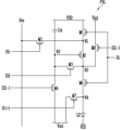
일 실시예에 의하면, 상기 화소들 중 i(단, i는 자연수)번째 수평라인에 위치하는 화소들 각각은, 제1 전극 및 제2 전원에 접속되는 제2 전극을 포함하는 발광 소자; 제1 전원에 전기적으로 연결되는 제1 노드에 접속되는 제1 전극을 포함하며, 제2 노드의 전압에 기초하여 구동 전류를 제어하는 제1 트랜지스터; 데이터선과 상기 제1 노드 사이에 접속되며, i번째 제1 주사선으로 공급되는 제1 주사 신호에 의해 턴-온되는 제2 트랜지스터; 상기 제1 트랜지스터의 제2 전극에 접속되는 제3 노드와 상기 제2 노드 사이에 접속되며, i번째 제2 주사선으로 공급되는 제2 주사 신호에 의해 턴-온되는 제3 트랜지스터; 상기 제2 노드와 제1 초기화 전원 사이에 접속되며, i번째 제3 주사선으로 공급되는 제3 주사 신호에 의해 턴-온되는 제4 트랜지스터; 및 상기 제1 전원과 상기 제1 노드 사이에 접속되며, i번째 발광 제어선으로 공급되는 상기 발광 제어 신호에 의해 턴-오프되는 제5 트랜지스터를 포함할 수 있다. According to one embodiment, each of the pixels located on the i (where i is a natural number)-th horizontal line is a light emitting element including a first electrode and a second electrode connected to a second power source; a first transistor including a first electrode connected to a first node electrically connected to a first power source and controlling a driving current based on the voltage of the second node; a second transistor connected between a data line and the first node and turned on by a first scan signal supplied to the i-th first scan line; a third transistor connected between a third node connected to the second electrode of the first transistor and the second node, and turned on by a second scan signal supplied to the i-th second scan line; a fourth transistor connected between the second node and the first initialization power supply and turned on by a third scan signal supplied to the ith third scan line; and a fifth transistor connected between the first power source and the first node and turned off by the emission control signal supplied to the i-th emission control line.
일 실시예에 의하면, 상기 표시 장치는, 상기 화소들에 연결되는 제3 주사선들 각각에 상기 제2 주파수로 제3 주사 신호를 공급하는 제3 주사 구동부를 더 포함할 수 있다. 상기 제2 및 제3 주사 신호들의 폭들은 상기 제1 주사 신호의 폭보다 길 수 있다. According to one embodiment, the display device may further include a third scan driver that supplies a third scan signal at the second frequency to each of the third scan lines connected to the pixels. The widths of the second and third scan signals may be longer than the width of the first scan signal.
일 실시예에 의하면, 상기 구동 주파수로 구동될 때, 상기 제2 및 제3 주사 구동부들은 한 프레임 기간 내의 제1 기간 동안 상기 제2 및 제3 주사 신호들을 각각 공급할 수 있다. 상기 구동 주파수로 구동될 때, 상기 제2 및 제3 주사 구동부들은 상기 한 프레임 기간 내의 제2 기간 동안 상기 제1 및 제2 주사 신호들을 공급하지 않는다. According to one embodiment, when driven at the driving frequency, the second and third scan drivers may supply the second and third scan signals, respectively, during a first period within one frame period. When driven at the driving frequency, the second and third scan drivers do not supply the first and second scan signals during a second period within the one frame period.
일 실시예에 의하면, 상기 제1 기간에서, 상기 i번째 제2 주사선으로 공급되는 상기 제2 주사 신호와 상기 i번째 제3 주사선으로 공급되는 상기 제3 주사 신호는 중첩하지 않는다. According to one embodiment, in the first period, the second scan signal supplied to the ith second scan line and the third scan signal supplied to the ith third scan line do not overlap.
일 실시예에 의하면, 상기 제1 기간에서, 상기 i번째 제3 주사선으로 공급되는 상기 제3 주사 신호는 상기 i번째 제2 주사선으로 공급되는 상기 제2 주사 신호의 일부와 중첩하며, 상기 i번째 제1 주사선으로 공급되는 상기 제1 주사 신호는 상기 i번째 제2 주사선으로 공급되는 상기 제2 주사 신호의 다른 일부와 중첩할 수 있다. According to one embodiment, in the first period, the third scan signal supplied to the i-th third scan line overlaps a portion of the second scan signal supplied to the i-th second scan line, and The first scan signal supplied to the first scan line may overlap with another part of the second scan signal supplied to the ith second scan line.
본 발명의 실시예들에 따른 표지 장치는 하나의 프레임에 하나의 표시 스캔 기간과 적어도 하나의 자가 스캔 기간을 포함함으로써 다양한 구동 주파수들의 영상 출력이 지원될 수 있다. 또한, 구동 주파수가 감소할수록 자가 스캔 기간의 개수가 증가됨으로써, 저주파수 구동에서의 휘도 감소 및 플리커 시인이 개선될 수 있다.The sign device according to embodiments of the present invention can support image output at various driving frequencies by including one display scan period and at least one self-scan period in one frame. Additionally, as the driving frequency decreases, the number of self-scan periods increases, thereby improving luminance reduction and flicker visibility in low-frequency driving.
나아가, 주기적으로 제1 트랜지스터에 소정의 바이어스를 인가함으로써 소비 전력이 개선됨과 동시에 저주파수 구동에서의 플리커가 개선될 수 있다.Furthermore, by periodically applying a predetermined bias to the first transistor, power consumption can be improved and flicker in low-frequency driving can be improved.
다만, 본 발명의 효과는 상술한 효과에 한정되는 것이 아니며, 본 발명의 사상 및 영역으로부터 벗어나지 않는 범위에서 다양하게 확장될 수 있을 것이다.However, the effects of the present invention are not limited to the effects described above, and may be expanded in various ways without departing from the spirit and scope of the present invention.
도 1은 본 발명의 실시예들에 따른 표시 장치를 나타내는 블록도이다.
도 2는 도 1의 표시 장치에 포함되는 화소의 일 예를 나타내는 회로도이다.
도 3a는 도 2의 화소의 구동의 일 예를 나타내는 타이밍도이다.
도 3b는 도 2의 화소의 구동의 일 예를 나타내는 타이밍도이다.
도 4는 도 1의 표시 장치가 제1 구동 주파수로 구동될 때의 구동 방법의 일 예를 나타내는 타이밍도이다.
도 5는 도 1의 표시 장치가 제2 구동 주파수로 구동될 때의 구동 방법의 일 예를 나타내는 타이밍도이다.
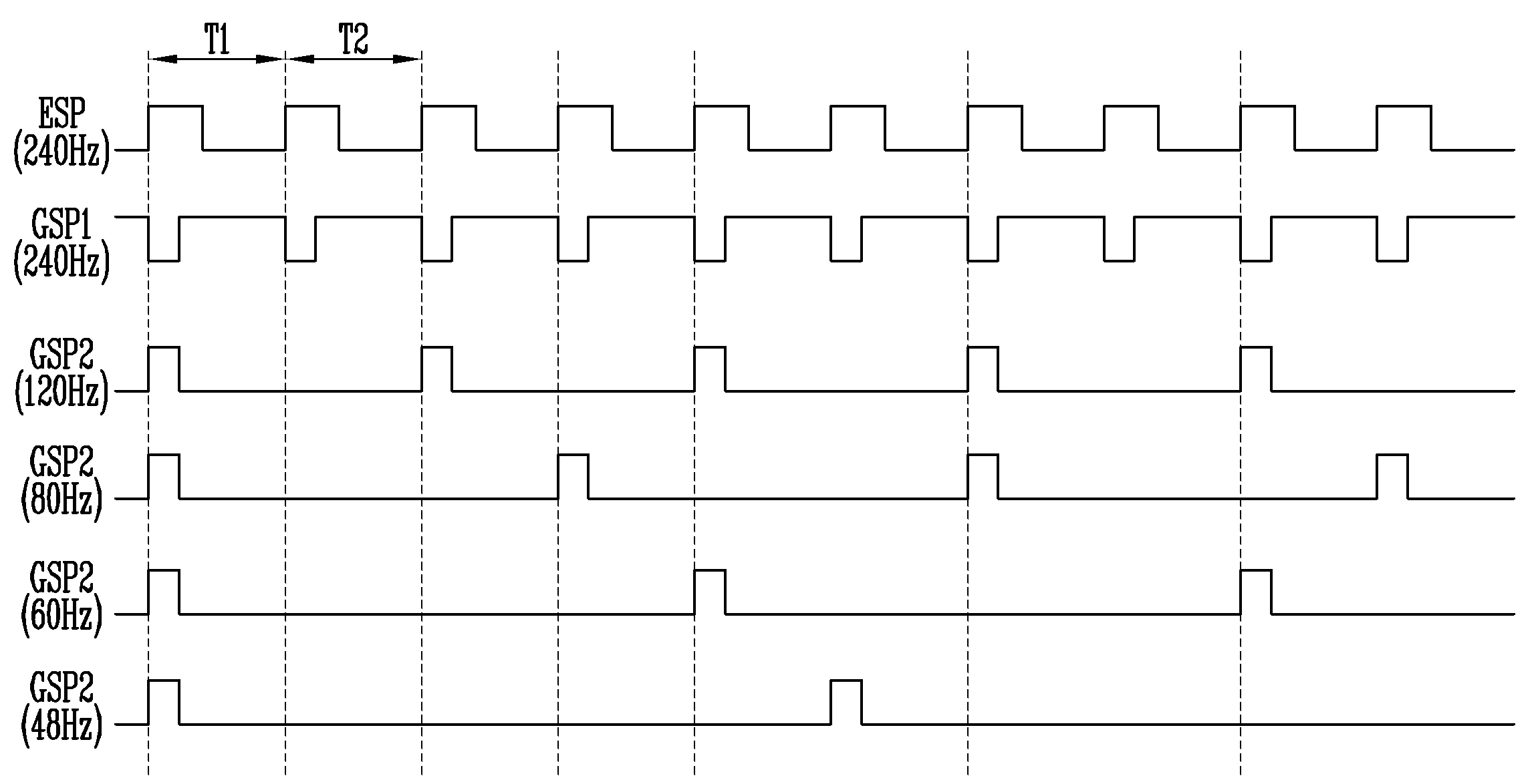
도 6a는 구동 주파수에 따라 표시 장치에 포함되는 발광 구동부 및 주사 구동부들로 공급되는 게이트 스타트 펄스들의 일 예를 나타내는 타이밍도이다.
도 6b는 구동 주파수에 따른 표시 장치의 구동 방법의 일 예를 설명하기 위한 개념도이다.
도 7은 도 1의 표시 장치에 포함되는 화소의 일 예를 나타내는 회로도이다.
도 8은 도 1의 표시 장치에 포함되는 화소의 일 예를 나타내는 회로도이다.
도 9는 도 1의 표시 장치에 포함되는 화소의 일 예를 나타내는 회로도이다.
도 10a는 도 9의 화소의 구동의 일 예를 나타내는 타이밍도이다.
도 10b는 도 9의 화소의 구동의 일 예를 나타내는 타이밍도이다.
도 11은 도 1의 표시 장치에 포함되는 화소의 일 예를 나타내는 회로도이다.
도 12는 도 11의 화소의 구동의 일 예를 나타내는 타이밍도이다.
도 13은 본 발명의 실시예들에 따른 표시 장치를 나타내는 블록도이다.
도 14는 도 13의 표시 장치에 포함되는 화소의 일 예를 나타내는 회로도이다.
도 15a 내지 도 15c는 도 14의 화소의 구동의 일 예들을 나타내는 타이밍도들이다.
도 16은 도 1의 표시 장치에 포함되는 화소의 일 예를 나타내는 회로도이다.
도 17a 및 도 17b는 도 16의 화소의 구동의 일 예들을 나타내는 타이밍도들이다.
도 18은 도 1의 표시 장치에 포함되는 화소의 일 예를 나타내는 회로도이다.
도 19a 및 도 19b는 도 18의 화소의 구동의 일 예들을 나타내는 타이밍도들이다.1 is a block diagram showing a display device according to embodiments of the present invention.
FIG. 2 is a circuit diagram illustrating an example of a pixel included in the display device of FIG. 1 .
FIG. 3A is a timing diagram illustrating an example of driving the pixel of FIG. 2.
FIG. 3B is a timing diagram illustrating an example of driving the pixel of FIG. 2.
FIG. 4 is a timing diagram illustrating an example of a driving method when the display device of FIG. 1 is driven at a first driving frequency.
FIG. 5 is a timing diagram illustrating an example of a driving method when the display device of FIG. 1 is driven at a second driving frequency.
FIG. 6A is a timing diagram illustrating an example of gate start pulses supplied to the light emission driver and scan driver included in the display device according to the driving frequency.
FIG. 6B is a conceptual diagram illustrating an example of a method of driving a display device according to a driving frequency.
FIG. 7 is a circuit diagram illustrating an example of a pixel included in the display device of FIG. 1 .
FIG. 8 is a circuit diagram illustrating an example of a pixel included in the display device of FIG. 1 .
FIG. 9 is a circuit diagram illustrating an example of a pixel included in the display device of FIG. 1 .
FIG. 10A is a timing diagram illustrating an example of driving the pixel of FIG. 9.
FIG. 10B is a timing diagram showing an example of driving the pixel of FIG. 9.
FIG. 11 is a circuit diagram illustrating an example of a pixel included in the display device of FIG. 1 .
FIG. 12 is a timing diagram showing an example of driving the pixel of FIG. 11.
Figure 13 is a block diagram showing a display device according to embodiments of the present invention.
FIG. 14 is a circuit diagram showing an example of a pixel included in the display device of FIG. 13.
FIGS. 15A to 15C are timing diagrams showing examples of driving the pixel of FIG. 14 .
FIG. 16 is a circuit diagram illustrating an example of a pixel included in the display device of FIG. 1 .
FIGS. 17A and 17B are timing diagrams showing examples of driving the pixel of FIG. 16 .
FIG. 18 is a circuit diagram illustrating an example of a pixel included in the display device of FIG. 1.
FIGS. 19A and 19B are timing diagrams showing examples of driving the pixel of FIG. 18.
이하, 첨부한 도면들을 참조하여, 본 발명의 바람직한 실시예를 보다 상세하게 설명하고자 한다. 도면상의 동일한 구성요소에 대해서는 동일한 참조부호를 사용하고 동일한 구성요소에 대해서 중복된 설명은 생략한다.Hereinafter, preferred embodiments of the present invention will be described in more detail with reference to the attached drawings. The same reference numerals are used for the same components in the drawings, and duplicate descriptions for the same components are omitted.
도 1은 본 발명의 실시예들에 따른 표시 장치를 나타내는 블록도이다.1 is a block diagram showing a display device according to embodiments of the present invention.
도 1을 참조하면, 표시 장치(1000)는 화소부(100), 제1 주사 구동부(200), 제2 주사 구동부(300), 발광 구동부(400), 데이터 구동부(500), 및 타이밍 제어부(600)를 구비한다. Referring to FIG. 1, the
표시 장치(1000)는 구동 조건에 따라 다양한 구동 주파수로 영상을 표시할 수 있다. 일 실시예에서, 표시 장치(1000)는 구동 조건에 따라 제2 주사 구동부(200)의 출력 주파수 및 이에 대응하는 데이터 구동부(500)의 출력 주파수를 조절할 수 있다. 예를 들어, 표시 장치(1000)는 1Hz 내지 120Hz의 다양한 구동 주파수들에 대응하여 영상을 표시할 수 있다. The
타이밍 제어부(600)는 소정의 인터페이스를 통해 AP(Application processor)와 같은 호스트 시스템으로부터 입력 영상 데이터(IRGB) 및 타이밍 신호들(Vsync, Hsync, DE, CLK)을 공급받을 수 있다. The
타이밍 제어부(600)는 입력 영상 데이터(IRGB), 수직동기신호(Vsync), 수평동기신호(Hsync), 데이터 인에이블 신호(DE) 및 클럭 신호(CLK) 등의 타이밍 신호들에 기초하여 데이터 구동 제어 신호(DCS)를 생성할 수 있다. 데이터 구동 제어 신호(DCS)는 데이터 구동부(500)로 공급될 수 있다. 그리고, 타이밍 제어부(600)는 입력 영상 데이터(IRGB)를 재정렬하여 데이터 구동부(500)로 공급한다.The
타이밍 제어부(600)는 타이밍 신호들에 기초하여 게이트 스타트 펄스들(GSP1, GSP2) 및 클럭 신호(CLK)들을 제1 주사 구동부(200) 및 제2 주사 구동부(300)로 공급한다. The
타이밍 제어부(600)는 타이밍 신호들에 기초하여 발광 스타트 펄스(ESP) 및 클럭 신호(CLK)들을 발광 구동부(400)로 공급한다. 발광 스타트 펄스는 발광 제어 신호의 첫 번째 타이밍을 제어한다. 클럭 신호들은 발광 스타트 펄스를 쉬프트시키기 위하여 사용된다. The
제1 게이트 스타트 펄스(GSP1)는 제1 주사 구동부(200)로부터 공급되는 주사 신호의 첫 번째 타이밍을 제어한다. 클럭 신호(CLK)들은 제1 게이트 스타트 펄스(GSP1)를 쉬프트시키기 위하여 사용된다.The first gate start pulse GSP1 controls the first timing of the scan signal supplied from the
제2 게이트 스타트 펄스(GSP2)는 제2 주사 구동부(300)로부터 공급되는 주사 신호의 첫 번째 타이밍을 제어한다. 클럭 신호(CLK)들은 제2 게이트 스타트 펄스(GSP2)를 쉬프트시키기 위하여 사용된다. The second gate start pulse (GSP2) controls the first timing of the scan signal supplied from the
데이터 구동부(500)는 데이터 구동 제어 신호(DCS)에 대응하여 데이터선(D)들로 데이터 신호를 공급한다. 데이터선(D)들로 공급된 데이터 신호는 주사 신호에 의하여 선택된 화소(PXL)들로 공급된다. The
데이터 구동부(500)는 구동 주파수에 대응하여 한 프레임 기간 동안 데이터선(D)들로 데이터 신호를 공급한다. 예를 들어, 데이터 구동부(500)는 표시 장치(1000)가 제1 구동 주파수로 구동될 때 한 프레임 기간 동안 데이터선(D)들로 데이터 신호를 공급한다. 이때, 데이터선(D)들로 공급되는 데이터 신호는 제1 주사선(S1)들 및 제2 주사선(S2)들로 공급되는 주사 신호와 동기되도록 공급될 수 있다.The
데이터 구동부(500)는 한 프레임 기간 중 제2 주사선(S2)들로 주사 신호가 공급되는 제1 기간 동안 데이터선(D)들로 데이터 신호를 공급하고, 제1 기간을 제외한 제2 기간 동안 데이터선(D)들로 임의의 기준 전압을 공급할 수 있다. 예를 들어, 기준 전압은 데이터 신호들의 전압범위 내의 특정 전압으로 설정될 수 있다. 예를 들어, 기준 전압은 블랙 계조의 데이터 전압으로 설정될 수 있다. 또한, 기준 전압은 데이터 신호들의 전압범위 내에서 수평 기간의 경과 또는 프레임의 경과에 따라 자유롭게 변경될 수 있다. The
추가적으로, 제1 기간은 제1 주사선(S1)들 및 제2 주사선(S2)들 모두로 주사 신호가 공급되는 기간을 의미한다. 그리고, 제2 기간은 제1 주사선(S1)들로 주사 신호가 공급되는 기간을 의미한다.Additionally, the first period refers to a period in which scan signals are supplied to both the first scan lines S1 and the second scan lines S2. And, the second period refers to a period in which scan signals are supplied to the first scan lines S1.
제1 주사 구동부(200)는 제1 게이트 스타트 펄스(GSP1)에 대응하여 제1 주사선(S1)들로 주사 신호를 공급한다. 일례로, 제1 주사 구동부(200)는 제1 주사선(S1)들로 주사 신호를 순차적으로 공급할 수 있다. 여기서, 제1 주사 구동부(200)로부터 공급되는 주사 신호는 화소(PXL)에 포함된 트랜지스터가 턴-온될 수 있도록 게이트 온 전압으로 설정된다. The
한편, 제1 주사 구동부(200)는 표시 장치(1000)의 영상 프레임(또는 프레임 주파수)에 대응하는 구동 주파수와 관계없이 항상 일정한 제1 주파수로 주사 신호를 제1 주사선(S1)들로 공급할 수 있다. 여기서, 제1 주파수는 타이밍 제어부(600)로부터 제1 주사 구동부(200)로 공급되는 제1 게이트 스타트 펄스(GSP1)의 출력 주파수에 상응할 수 있다. Meanwhile, the
또한, 제1 주사 구동부(200)가 주사 신호를 공급하는 제1 주파수는 구동 주파수보다 크다. 일 실시예에서, 구동 주파수는 제1 주파수의 약수로 설정될 수 있다. 예를 들어, 제1 주파수는 표시 장치(1000)의 최대 구동 주파수의 약 2배로 설정될 수 있다. 표시 장치(1000)의 최대 구동 주파수가 약 120Hz인 경우, 제1 주파수는 약 240Hz로 설정될 수 있다. 따라서, 한 프레임 기간 내에서 제1 주사선(S1)들로 주사 신호가 순차적으로 출력되는 스캐닝 동작이 소정 주기로 복수회 반복될 수 있다. 즉, 한 프레임 기간 내에서, 제1 주사선(S1)들 각각으로 공급되는 주사 신호는 소정 주기마다 반복적으로 공급될 수 있다.Additionally, the first frequency at which the
예를 들어, 표시 장치(1000)가 구동 가능한 모든 구동 주파수들에서, 제1 주사 구동부(200)는 제1 기간 동안 스캐닝을 1회 수행하며, 제2 기간 동안 구동 주파수에 따라 스캐닝을 적어도 1회 수행할 수 있다. 즉, 제1 기간 동안 제1 주사선(S1)들 각각으로 주사 신호가 순차적으로 1회 출력되고, 제2 기간 동안 제1 주사선(S1)들 각각으로 주사 신호가 순차적으로 적어도 1회 출력될 수 있다. For example, at all driving frequencies at which the
또한, 구동 주파수가 감소되는 경우, 하나의 프레임 기간 내에서 제1 주사 구동부(200)가 제1 주사선(S1)들 각각으로 주사 신호를 공급하는 동작의 반복 횟수가 증가될 수 있다. Additionally, when the driving frequency is reduced, the number of repetitions of the operation of the
제2 주사 구동부(300)는 제2 게이트 스타트 펄스(GSP2)에 대응하여 제2 주사선(S2)들로 주사 신호를 공급한다. 일례로, 제2 주사 구동부(300)는 제2 주사선(S2)들로 주사 신호를 순차적으로 공급할 수 있다. 여기서, 제2 주사 구동부(300)로부터 공급되는 주사 신호는 화소(PXL)에 포함된 트랜지스터가 턴-온될 수 있도록 게이트 온 전압으로 설정된다. The
제2 주사 구동부(300)는 표시 장치(1000)의 영상 프레임(또는 프레임 주파수)에 대응하는 구동 주파수와 동일한 주파수(예를 들어, 제2 주파수)로 주사 신호를 제2 주사선(S2)들로 공급할 수 있다. 일 실시예에서, 제2 주파수는 타이밍 제어부(600)로부터 제2 주사 구동부(300)로 공급되는 제2 게이트 스타트 펄스(GSP2)의 출력 주파수에 상응할 수 있다. The
구동 주파수와 실질적으로 동일한 제2 주파수는 제1 주파수의 약수로 설정될 수 있다. The second frequency that is substantially equal to the driving frequency may be set as a divisor of the first frequency.
제 2주사 구동부(300)는 한 프레임의 제1 기간 동안 제2 주사선(S2)들로 주사 신호를 공급한다. 일례로, 제2 주사 구동부(300)는 제1 기간 동안 제2 주사선(S2)들 각각으로 적어도 하나의 주사 신호를 공급할 수 있다. 여기서, 제1 기간 동안 i번째 제1 주사선(S1i)으로 공급되는 주사 신호는 i번째 제2 주사선(S2i)으로 공급되는 주사 신호와 중첩할 수 있다.The
발광 구동부(400)는 발광 스타트 펄스(ESP)에 대응하여 발광 제어선(E)들로 발광 제어 신호를 공급한다. 일례로, 발광 구동부(400)는 발광 제어선(E)들로 발광 제어 신호를 순차적으로 공급할 수 있다. 발광 제어선(E)들로 발광 제어 신호가 순차적으로 공급되면 화소(PXL)들이 수평라인 단위로 비발광된다. 이를 위하여 발광 제어 신호는 화소(PXL)들에 포함된 트랜지스터가 턴-오프될 수 있도록 게이트 오프 전압으로 설정된다. 일 실시예에서, 발광 구동부(400)는 i-1번째 제1 주사선(S1i-1)(및/또는 i-1번째 제2 주사선(S2i-1)), i번째 제1 주사선(S1i)(및/또는 i번째 제2 주사선(S2i)), 및 i+1번째 제1 주사선(S1i+1)(및/또는 i+1번째 제2 주사선(S2i+1))으로 공급되는 주사 신호와 중첩되도록 i번째 발광 제어선(Ei)으로 발광 제어 신호를 공급한다. The
일 실시예에서, 제1 주사 구동부(200)와 마찬가지로, 발광 구동부(400)는 제1 주파수로 발광 제어 신호를 발광 제어선(E)들에 공급할 수 있다. 따라서, 한 프레임 기간 내에서, 발광 제어선(E)들 각각으로 공급되는 발광 제어 신호는 소정 주기마다 반복적으로 공급될 수 있다. In one embodiment, like the
이에 따라, 구동 주파수가 감소되는 경우, 하나의 프레임 기간 내에서 발광 구동부(400)가 발광 제어선(E)들 각각으로 발광 제어 신호를 공급하는 동작의 반복 횟수가 증가될 수 있다. Accordingly, when the driving frequency is reduced, the number of repetitions of the operation of the
화소부(100)는 데이터선(D)들, 주사선들(S1, S2) 및 발광 제어선(E)들에 접속되도록 위치되는 화소(PXL)들을 구비한다. 화소(PXL)들은 외부로부터 제1 전원(VDD), 제2 전원(VSS), 및 초기화 전원(Vint)의 전압들을 공급받을 수 있다. The
화소(PXL)들 각각은 자신과 접속된 주사선들(S1, S2)로 주사 신호가 공급될 때 선택되어 데이터선(D)으로부터 데이터 신호를 공급받는다. 데이터 신호를 공급받은 화소(PXL)는 데이터 신호에 대응하여 제1 전원(VDD)으로부터 발광 소자를 경유하여 제2 전원(VSS)으로 흐르는 전류량을 제어한다. 발광 소자는 전류량에 대응하여 소정 휘도의 빛을 생성한다. 화소(PXL)들 각각의 발광 시간은 자신과 접속된 발광 제어선(E)으로부터 공급되는 발광 제어 신호에 의하여 제어된다. Each of the pixels PXL is selected when a scan signal is supplied to the scan lines S1 and S2 connected to the pixel PXL, and receives a data signal from the data line D. The pixel (PXL) that receives the data signal controls the amount of current flowing from the first power source (VDD) to the second power source (VSS) via the light emitting device in response to the data signal. The light emitting element generates light of a certain brightness in response to the amount of current. The emission time of each pixel (PXL) is controlled by the emission control signal supplied from the emission control line (E) connected to the pixel (PXL).
추가적으로, 화소(PXL)들은 화소 회로 구조에 대응하여 하나 이상의 제1 주사선(S1), 제2 주사선(S2) 및 발광 제어선(E)에 접속될 수 있다. 즉, 본 발명의 실시예에서는 화소(PXL)의 회로구조에 대응하여 화소(PXL)에 접속되는 신호선들(S1, S2, E, D)은 다양하게 설정될 수 있다. Additionally, the pixels (PXL) may be connected to one or more of the first scan line (S1), the second scan line (S2), and the emission control line (E) corresponding to the pixel circuit structure. That is, in the embodiment of the present invention, the signal lines S1, S2, E, and D connected to the pixel PXL can be set in various ways according to the circuit structure of the pixel PXL.
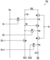
도 2는 도 1의 표시 장치에 포함되는 화소의 일 예를 나타내는 회로도이다. FIG. 2 is a circuit diagram illustrating an example of a pixel included in the display device of FIG. 1 .
도 2에서는 설명의 편의를 위하여 i번째 수평라인에 위치되며, 제m 데이터선(Dm)과 접속된 화소를 도시하기로 한다.In Figure 2, for convenience of explanation, a pixel located on the i-th horizontal line and connected to the m-th data line (Dm) is shown.
도 2를 참조하면, 화소(PXL)는 발광 소자(LD), 제1 내지 제7 트랜지스터들(M1 내지 M7), 및 스토리지 커패시터(Cst)를 포함할 수 있다. Referring to FIG. 2 , the pixel PXL may include a light emitting device LD, first to seventh transistors M1 to M7, and a storage capacitor Cst.
발광 소자(LD)의 제1 전극(애노드 전극 또는 캐소드 전극)은 제4 노드(N4)에 접속되고 제1 전극(캐소드 전극 또는 애노드 전극)은 제2 전원(VSS)에 접속된다. 발광 소자(LD)는 제1 트랜지스터(M1)로부터 공급되는 전류량에 대응하여 소정 휘도의 빛을 생성한다.The first electrode (anode electrode or cathode electrode) of the light emitting element LD is connected to the fourth node N4, and the first electrode (cathode electrode or anode electrode) is connected to the second power source VSS. The light emitting device LD generates light with a predetermined brightness in response to the amount of current supplied from the first transistor M1.
일 실시예에서, 발광 소자(LD)는 유기 발광층을 포함하는 유기 발광 다이오드일 수 있다. 다른 실시예에서, 발광 소자(LD)는 무기 물질로 형성되는 무기 발광 소자일 수 있다. 또는 발광 소자(LD)는 복수의 무기 발광 소자들이 제2 전원(VSS)과 제4 노드(N4) 사이에 병렬 및/또는 직렬로 연결된 형태를 가질 수도 있다. In one embodiment, the light emitting device LD may be an organic light emitting diode including an organic light emitting layer. In another embodiment, the light emitting device LD may be an inorganic light emitting device made of an inorganic material. Alternatively, the light emitting device LD may have a plurality of inorganic light emitting devices connected in parallel and/or series between the second power source VSS and the fourth node N4.
제1 트랜지스터(M1)(또는 구동 트랜지스터)의 제1 전극은 제1 노드(N1)에 접속되고, 제2 전극은 제3 노드(N3)에 접속된다. 제1 트랜지스터(M1)의 게이트 전극은 제2 노드(N2)에 접속된다. 제1 트랜지스터(M1)는 제2 노드(N2)의 전압에 대응하여 제1 전원(VDD)으로부터 발광 소자(LD)를 경유하여 제2 전원(VSS)으로 흐르는 전류량을 제어할 수 있다. 이를 위하여, 제1 전원(VDD)은 제2 전원(VSS)보다 높은 전압으로 설정될 수 있다. The first electrode of the first transistor M1 (or driving transistor) is connected to the first node N1, and the second electrode is connected to the third node N3. The gate electrode of the first transistor (M1) is connected to the second node (N2). The first transistor M1 may control the amount of current flowing from the first power source VDD to the second power source VSS via the light emitting device LD in response to the voltage of the second node N2. To this end, the first power source (VDD) may be set to a higher voltage than the second power source (VSS).
제2 트랜지스터(M2)는 데이터선(Dm)과 제1 노드(N1) 사이에 접속된다. 제2 트랜지스터(M2)의 게이트 전극은 i번째 제1 주사선(S1i)에 접속된다. 제2 트랜지스터(M2)는 i번째 제1 주사선(S1i)으로 주사 신호가 공급될 때 턴-온되어 데이터선(Dm)과 제1 노드(N1)를 전기적으로 접속시킨다. The second transistor M2 is connected between the data line Dm and the first node N1. The gate electrode of the second transistor M2 is connected to the ith first scan line S1i. The second transistor M2 is turned on when a scan signal is supplied to the ith first scan line S1i and electrically connects the data line Dm and the first node N1.
제3 트랜지스터(M3)는 제1 트랜지스터(M1)의 제2 전극(즉, 제3 노드)(N3))과 제2 노드(N2) 사이에 접속된다. 제3 트랜지스터(M3)의 게이트 전극은 i번째 제2 주사선(S2i)에 접속된다. 제3 트랜지스터(M3)는 i번째 제2 주사선(S2i)으로 주사 신호가 공급될 때 턴-온되어 제1 트랜지스터(M1)의 제2 전극과 제2 노드(N2)를 전기적으로 접속시킨다. 따라서, 제3 트랜지스터(M3)가 턴-온되면 제1 트랜지스터(M1)는 다이오드 형태로 접속된다.The third transistor M3 is connected between the second electrode (i.e., third node) N3) of the first transistor M1 and the second node N2. The gate electrode of the third transistor M3 is connected to the ith second scan line S2i. The third transistor M3 is turned on when a scan signal is supplied to the ith second scan line S2i and electrically connects the second electrode of the first transistor M1 to the second node N2. Accordingly, when the third transistor M3 is turned on, the first transistor M1 is connected in the form of a diode.
제4 트랜지스터(M4)는 제2 노드(N2)와 제1 초기화 전원(Vint1) 사이에 접속된다. 제4 트랜지스터(M4)의 게이트 전극은 i-1번째 제2 주사선(S2i-1)에 접속된다. 제4 트랜지스터(M4)는 i-1번째 제2 주사선(S2i-1)으로 주사 신호가 공급될 때 턴-온되어 제1 초기화 전원(Vint1)의 전압을 제2 노드(N2)로 공급한다. 여기서, 제1 초기화 전원(Vint1)의 전압은 데이터선(Dm)으로 공급되는 데이터 신호보다 낮은 전압으로 설정된다.The fourth transistor M4 is connected between the second node N2 and the first initialization power supply Vint1. The gate electrode of the fourth transistor M4 is connected to the i-1th second scan line S2i-1. The fourth transistor M4 is turned on when a scan signal is supplied to the i-1th second scan line S2i-1 and supplies the voltage of the first initialization power supply Vint1 to the second node N2. Here, the voltage of the first initialization power supply Vint1 is set to a lower voltage than the data signal supplied to the data line Dm.
이에 따라, 제4 트랜지스터(M4)의 턴-온에 의해 제1 트랜지스터(M1)의 게이트 전압이 제1 초기화 전원(Vint1)의 전압으로 초기화되고, 제1 트랜지스터(M1)가 온-바이어스(on-bias) 상태를 가질 수 있다(즉, 온-바이어스 상태로 초기화됨). Accordingly, by turning on the fourth transistor M4, the gate voltage of the first transistor M1 is initialized to the voltage of the first initialization power supply Vint1, and the first transistor M1 is turned on. -bias) state (i.e. initialized to the on-bias state).
제5 트랜지스터(M5)는 제1 전원(VDD)과 제1 노드(N1) 사이에 접속된다. 제5 트랜지스터(M5)의 게이트 전극은 발광 제어선(Ei)에 접속된다. 제5 트랜지스터(M5)는 발광 제어선(Ei)으로 발광 제어 신호가 공급될 때 턴-오프되고, 그 외의 경우에 턴-온된다. The fifth transistor M5 is connected between the first power source VDD and the first node N1. The gate electrode of the fifth transistor M5 is connected to the emission control line Ei. The fifth transistor M5 is turned off when the emission control signal is supplied to the emission control line Ei, and is turned on in other cases.
제6 트랜지스터(M6)는 제1 트랜지스터(M1)의 제2 전극(즉, 제3 노드(N3))과 발광 소자(LD)의 제1 전극(즉, 제4 노드(N4)) 사이에 접속된다. 제6 트랜지스터(M6)의 게이트 전극은 발광 제어선(Ei)에 접속된다. 제6 트랜지스터(M6)는 발광 제어선(Ei)으로 발광 제어 신호가 공급될 때 턴-오프되고, 그 외의 경우에 턴-온된다. The sixth transistor M6 is connected between the second electrode (i.e., third node (N3)) of the first transistor (M1) and the first electrode (i.e., fourth node (N4)) of the light emitting device (LD). do. The gate electrode of the sixth transistor M6 is connected to the emission control line Ei. The sixth transistor M6 is turned off when the emission control signal is supplied to the emission control line Ei, and is turned on in other cases.
제7 트랜지스터(M7)는 발광 소자(LD)의 제1 전극(즉, 제4 노드(N40))와 제2 초기화 전원(Vint2) 사이에 접속된다. 제7 트랜지스터(M7)의 게이트 전극은 i+1번째 제1 주사선(S1i+1)에 접속된다. 제7 트랜지스터(M7)는 i+1번째 제1 주사선(S1i+1)으로 주사 신호가 공급될 때 턴-온되어 제2 초기화 전원(Vint2)의 전압을 발광 소자(LD)의 제1 전극으로 공급한다. The seventh transistor M7 is connected between the first electrode (that is, the fourth node N40) of the light emitting device LD and the second initialization power supply Vint2. The gate electrode of the seventh transistor M7 is connected to the i+1th first scan
다만, 이는 예시적인 것으로서, 제7 트랜지스터(M7)의 게이트 전극은 i-1번째 제1 주사선(S1i-1) 또는 i번째 제1 주사선(Sli)에 연결될 수도 있다. However, this is an example, and the gate electrode of the seventh transistor M7 may be connected to the i-1th first scan line S1i-1 or the ith first scan line Sli.
발광 소자(LD)의 제1 전극으로 제1 초기화 전원(Vint2)의 전압이 공급되면, 발광 소자(LD)의 기생 커패시터가 방전될 수 있다. 기생 커패시터에 충전된 잔류 전압이 방전(제거)됨에 따라 의도치 않은 미세 발광이 방지될 수 있다. 따라서, 화소(PXL)의 블랙 표현 능력이 향상될 수 있다. When the voltage of the first initialization power source Vint2 is supplied to the first electrode of the light emitting device LD, the parasitic capacitor of the light emitting device LD may be discharged. As the residual voltage charged in the parasitic capacitor is discharged (removed), unintended micro-light emission can be prevented. Accordingly, the black expression ability of the pixel (PXL) can be improved.
한편, 제1 초기화 전원(Vint1)과 제2 초기화 전원(Vint2)은 서로 다른 전압을 생성할 수 있다. 즉, 제2 노드(N2)를 초기화하는 전압과 제4 노드(N4)를 초기화하는 전압은 서로 다르게 설정될 수 있다.Meanwhile, the first initialization power source Vint1 and the second initialization power source Vint2 may generate different voltages. That is, the voltage for initializing the second node N2 and the voltage for initializing the fourth node N4 may be set differently.
한 프레임 기간의 길이가 길어지는 저주파 구동에서, 제2 노드(N2)로 공급되는 제1 초기화 전원(Vint1)의 전압이 지나치게 낮은 경우, 해당 프레임 기간에서의 제1 트랜지스터(M1)의 히스테리시스 변화가 심해진다. 이러한 히스테리시스는 저주파 구동에서 플리커 현상을 야기할 수 있다. 따라서, 저주파 구동의 표시 장치에서는 제2 전원(VSS)의 전압보다 높은 제1 초기화 전원(Vint1)의 전압이 요구될 수 있다.In low-frequency driving where the length of one frame period is long, when the voltage of the first initialization power supply (Vint1) supplied to the second node (N2) is too low, the hysteresis change of the first transistor (M1) in the frame period It gets worse. This hysteresis can cause flicker in low-frequency driving. Accordingly, in a display device driven at a low frequency, the voltage of the first initialization power supply (Vint1) may be required to be higher than the voltage of the second power supply (VSS).
그러나, 제4 노드(N4)에 공급되는 제2 초기화 전원(Vint2)의 전압이 소정의 기준보다 높아지는 경우, 발광 소자(LD)의 기생 커패시터의 전압이 방전되지 않고 오히려 충전될 수 있다. 따라서, 제2 초기화 전원(Vint2)의 전압은 제2 전원(VSS)의 전압보다 낮아야 한다.However, when the voltage of the second initialization power supply Vint2 supplied to the fourth node N4 is higher than a predetermined standard, the voltage of the parasitic capacitor of the light emitting device LD may not be discharged but rather charged. Therefore, the voltage of the second initialization power supply (Vint2) must be lower than the voltage of the second power supply (VSS).
본 발명의 실시예들에 따른 표시 장치(1000)에 포함되는 화소(PXL)에는 서로 다른 전압을 제공하는 제1 초기화 전원(Vint1)과 제2 초기화 전원(Vint2)이 각각 연결될 수 있다. 따라서, 제1 트랜지스터(M1)를 초기화하는 전압 및 발광 소자(LD)를 초기화하는 전압이 독립적으로 결정됨으로써, 플리커 및 오발광이 개선될 수 있다. A first initialization power source Vint1 and a second initialization power source Vint2 providing different voltages may be connected to the pixel PXL included in the
스토리지 커패시터(Cst)는 제1 전원(VDD)과 제2 노드(N2) 사이에 접속된다. 스토리지 커패시터(Cst)는 제2 노드(N2)에 인가된 전압을 저장할 수 있다. The storage capacitor (Cst) is connected between the first power source (VDD) and the second node (N2). The storage capacitor Cst may store the voltage applied to the second node N2.
한편, 제1 트랜지스터(M1), 제2 트랜지스터(M2), 제5 트랜지스터(M5), 제6 트랜지스터(M6), 및 제7 트랜지스터(M7)는 폴리실리콘 반도체 트랜지스터로 형성될 수 있다. 예를 들어, 제1 트랜지스터(M1), 제2 트랜지스터(M2), 제5 트랜지스터(M5), 제6 트랜지스터(M6), 및 제7 트랜지스터(M7)는 액티브층(채널)로서 LTPS(low temperature poly-silicon) 공정을 통해 형성된 폴리실리콘 반도체층을 포함할 수 있다. 또한, 제1 트랜지스터(M1), 제2 트랜지스터(M2), 제5 트랜지스터(M5), 제6 트랜지스터(M6), 및 제7 트랜지스터(M7)는 P형 트랜지스터일 수 있다. 이에 따라, 제1 트랜지스터(M1), 제2 트랜지스터(M2), 제5 트랜지스터(M5), 제6 트랜지스터(M6), 및 제7 트랜지스터(M7)를 턴-온시키는 게이트 온 전압은 논리 로우 레벨일 수 있다. Meanwhile, the first transistor M1, the second transistor M2, the fifth transistor M5, the sixth transistor M6, and the seventh transistor M7 may be formed as polysilicon semiconductor transistors. For example, the first transistor (M1), the second transistor (M2), the fifth transistor (M5), the sixth transistor (M6), and the seventh transistor (M7) are active layers (channels) and have a low temperature (LTPS) It may include a polysilicon semiconductor layer formed through a poly-silicon) process. Additionally, the first transistor M1, the second transistor M2, the fifth transistor M5, the sixth transistor M6, and the seventh transistor M7 may be P-type transistors. Accordingly, the gate-on voltage that turns on the first transistor (M1), the second transistor (M2), the fifth transistor (M5), the sixth transistor (M6), and the seventh transistor (M7) is at a logic low level. It can be.
폴리실리콘 반도체 트랜지스터는 빠른 응답 속도의 장점이 있으므로, 빠른 스위칭이 요구되는 스위칭 소자에 적용될 수 있다. Polysilicon semiconductor transistors have the advantage of fast response speed, so they can be applied to switching devices that require fast switching.
제3 및 제4 트랜지스터들(M3, M4)은 산화물 반도체 트랜지스터로 형성될 수 있다. 예를 들어, 제3 및 제4 트랜지스터들(M3, M4)은 N형 산화물 반도체 트랜지스터일 수 있고, 액티브층으로서 산화물 반도체층을 포함할 수 있다. 이에 따라, 제3 및 제4 트랜지스터들(M3, M4)을 턴-온시키는 게이트 온 전압은 논리 하이 레벨일 수 있다. The third and fourth transistors M3 and M4 may be formed as oxide semiconductor transistors. For example, the third and fourth transistors M3 and M4 may be N-type oxide semiconductor transistors and may include an oxide semiconductor layer as an active layer. Accordingly, the gate-on voltage that turns on the third and fourth transistors M3 and M4 may be at a logic high level.
산화물 반도체 트랜지스터는 저온 공정이 가능하며, 폴리실리콘 반도체 트랜지스터에 비하여 낮은 전하 이동도를 갖는다. 즉, 산화물 반도체 트랜지스터는 오프 전류 특성이 우수하다. 따라서, 제3 트랜지스터(M3) 및 제4 트랜지스터(M4)를 산화물 반도체 트랜지스터로 형성하면 제2 노드(N2)로부터의 누설전류를 최소화할 수 있고, 이에 따라 표시품질을 향상시킬 수 있다. Oxide semiconductor transistors can be processed at low temperatures and have lower charge mobility than polysilicon semiconductor transistors. In other words, oxide semiconductor transistors have excellent off-current characteristics. Therefore, if the third transistor M3 and the fourth transistor M4 are formed of oxide semiconductor transistors, leakage current from the second node N2 can be minimized and display quality can be improved accordingly.
도 3a는 도 2의 화소의 구동의 일 예를 나타내는 타이밍도이다. FIG. 3A is a timing diagram illustrating an example of driving the pixel of FIG. 2.
도 2 및 도 3a를 참조하면, 화소(PXL)는 제1 기간 동안 영상 표시를 위한 신호들을 공급받을 수 있다. 제1 기간은 출력 영상에 실제로 대응하는 데이터 신호(DS)가 기입되는 기간을 포함할 수 있다. Referring to FIGS. 2 and 3A , the pixel PXL may receive signals for image display during the first period. The first period may include a period in which the data signal DS actually corresponding to the output image is written.
N형 트랜지스터인 제3 및 제4 트랜지스터들(M3, M4)에 연결되는 제2 주사선들(S2i, S2i-1)로 공급되는 주사 신호의 게이트-온 전압은 논리 하이 레벨이다. P형 트랜지스터인 제1, 제2, 제5, 제6, 및 제7 트랜지스터들(M1, M2, M5, M6, M7)에 연결되는 제1 주사선들(S1i, S1i+1)로 공급되는 주사 신호의 게이트-온 전압은 논리 로우 레벨이다. The gate-on voltage of the scan signal supplied to the second scan lines (S2i, S2i-1) connected to the third and fourth transistors (M3, M4), which are N-type transistors, is a logic high level. Scan supplied to the first scan lines (S1i, S1i+1) connected to the first, second, fifth, sixth, and seventh transistors (M1, M2, M5, M6, M7), which are P-type transistors. The gate-on voltage of the signal is at a logic low level.
먼저 발광 제어선(Ei)으로 발광 제어 신호가 공급된다. 발광 제어선(Ei)으로 발광 제어 신호가 공급되면 제5 및 제6 트랜지스터들(M5, M6)이 턴-오프된다. 제5 및 제6 트랜지스터들(M5, M6)이 턴-오프되면, 화소(PXL)는 비발광 상태로 설정된다. First, an emission control signal is supplied to the emission control line (Ei). When the emission control signal is supplied to the emission control line Ei, the fifth and sixth transistors M5 and M6 are turned off. When the fifth and sixth transistors M5 and M6 are turned off, the pixel PXL is set to a non-emission state.
이후, i-1번째 제2 주사선(S2i-1)으로 주사 신호가 공급된다. i-1번째 제2 주사선(S2i-1)으로 주사 신호가 공급되면 제4 트랜지스터(M4)가 턴-온된다. 제4 트랜지스터(M4)가 턴-온되면 제1 초기화 전원(Vint1)의 전압이 제2 노드(N2)로 공급된다.Afterwards, the scan signal is supplied to the i-1th second scan line (S2i-1). When a scan signal is supplied to the i-1th second scan line (S2i-1), the fourth transistor (M4) is turned on. When the fourth transistor M4 is turned on, the voltage of the first initialization power supply Vint1 is supplied to the second node N2.
이후, i번째 제1 주사선(S1i) 및 i번째 제2 주사선(S2i)으로 주사 신호가 공급된다. i번째 제2 주사선(S2i)으로 주사 신호가 공급되면 제3 트랜지스터(M3)가 턴-온된다. 제3 트랜지스터(M3)가 턴-온되면 제1 트랜지스터(M1)가 다이오드 형태로 접속되고, 제1 트랜지스터(M1)의 문턱전압이 보상될 수 있다. Afterwards, scanning signals are supplied to the i-th first scanning line (S1i) and the i-th second scanning line (S2i). When a scan signal is supplied to the ith second scan line (S2i), the third transistor (M3) is turned on. When the third transistor M3 is turned on, the first transistor M1 is connected in the form of a diode, and the threshold voltage of the first transistor M1 can be compensated.
i번째 제1 주사선(S1i)으로 주사 신호가 공급되면 제2 트랜지스터(M2)가 턴-온된다. 제2 트랜지스터(M2)가 턴-온되면 데이터선(Dm)으로부터의 데이터 신호(DS)가 제1 노드(N1)로 공급된다. 이때, 제2 노드(N2)가 데이터 신호(DS)보다 낮은 제1 초기화 전원(Vint1)의 전압으로 초기화되었기 때문에(예를 들어, 온-바이어스 상태로 초기화됨) 제1 트랜지스터(M1)가 턴-온된다.When a scan signal is supplied to the ith first scan line (S1i), the second transistor (M2) is turned on. When the second transistor M2 is turned on, the data signal DS from the data line Dm is supplied to the first node N1. At this time, because the second node N2 is initialized to the voltage of the first initialization power supply Vint1 lower than the data signal DS (for example, initialized to an on-bias state), the first transistor M1 is turned on. -It comes on.
제1 트랜지스터(M1)가 턴-온되면 제1 노드(N1)로 공급된 데이터 신호(DS)가 다이오드 형태로 접속된 제1 트랜지스터(M1)를 경유하여 제2 노드(N2)로 공급된다. 그러면, 제2 노드(N2)에는 데이터 신호(DS) 및 제1 트랜지스터(M1)의 문턱전압에 대응하는 전압이 인가된다. 이때, 스토리지 커패시터(Cst)는 제2 노드(N2)의 전압을 저장한다. When the first transistor M1 is turned on, the data signal DS supplied to the first node N1 is supplied to the second node N2 via the first transistor M1 connected in the form of a diode. Then, a voltage corresponding to the data signal DS and the threshold voltage of the first transistor M1 is applied to the second node N2. At this time, the storage capacitor Cst stores the voltage of the second node N2.
이후, i+1번째 제1 주사선(S1i+1)으로 주사 신호가 공급된다. i+1번째 제1 주사선(S1i+1)으로 주사 신호가 공급되면 제7 트랜지스터(M7)가 턴-온된다. 제7 트랜지스터(M7)가 턴-온되면 발광 소자(LD1)의 제1 전극(즉, 제4 노드(N4))으로 제2 초기화 전원(Vint2)의 전압이 공급된다. 이에 따라, 발광 소자(LD)의 기생 커패시터에 남아있던 잔류 전압이 방전될 수 있다. Afterwards, the scan signal is supplied to the i+1th first scan line (S1i+1). When a scan signal is supplied to the i+1th first scan line (S1i+1), the seventh transistor (M7) is turned on. When the seventh transistor M7 is turned on, the voltage of the second initialization power source Vint2 is supplied to the first electrode (that is, the fourth node N4) of the light emitting device LD1. Accordingly, the residual voltage remaining in the parasitic capacitor of the light emitting device LD may be discharged.
이후, 발광 제어선(Ei)으로 발광 제어 신호의 공급이 중단된다. 발광 제어선(Ei)으로 발광 제어 신호의 공급이 중단되면, 제5 및 제6 트랜지스터들(M5, M6)가 턴-온된다. 이때, 제1 트랜지스터(M1)는 제2 노드(N2)의 전압에 대응하여 발광 소자(LD)로 흐르는 구동 전류를 제어한다. 그러면, 발광 소자(LD)는 전류량에 대응하는 휘도의 빛을 생성한다. Afterwards, the supply of the emission control signal to the emission control line Ei is stopped. When the supply of the emission control signal to the emission control line Ei is stopped, the fifth and sixth transistors M5 and M6 are turned on. At this time, the first transistor M1 controls the driving current flowing to the light emitting device LD in response to the voltage of the second node N2. Then, the light emitting element LD generates light with a brightness corresponding to the amount of current.
도 3a에서는 설명의 편의성을 위하여 제1 기간 동안 주사선들(S1, S2) 각각으로 하나의 주사 신호가 공급되는 것으로 도시되었지만, 본 발명이 이에 한정되지는 않는다. 일례로, 주사선들(S1, S2) 각각으로는 복수 개의 주사 신호가 공급될 수도 있다. 이 경우에도 실질적인 동작과정은 도 3a와 동일하며 이에 따라 상세한 설명은 생략하기로 한다. 그리고, 이후 설명에서는 주사선들(S1, S2) 각각으로 하나의 주사 신호가 공급되는 것으로 가정하여 설명하기로 한다. In FIG. 3A , for convenience of explanation, one scan signal is shown to be supplied to each of the scan lines S1 and S2 during the first period, but the present invention is not limited thereto. For example, a plurality of scan signals may be supplied to each of the scan lines S1 and S2. In this case as well, the actual operating process is the same as that in FIG. 3A, so detailed description will be omitted. In the following description, it will be assumed that one scan signal is supplied to each of the scan lines S1 and S2.
이러한 제1 기간의 동작은 제2 주사선들(S2i-1, S2i)로 공급되는 주사 신호들에 의해 구현되며, 제2 주사 구동부(300)의 주파수에 동기할 수 있다. The operation in this first period is implemented by scan signals supplied to the second scan lines S2i-1 and S2i, and can be synchronized to the frequency of the
도 3b는 도 2의 화소의 구동의 일 예를 나타내는 타이밍도이다. FIG. 3B is a timing diagram illustrating an example of driving the pixel of FIG. 2.
도 2 및 도 3b를 참조하면, 제1 기간에서 출력되는 영상의 휘도를 유지하기 위해, 화소(PXL)는 제2 기간 동안 제1 트랜지스터(M1)의 제1 전극(예를 들어, 소스 전극)에 소정의 기준 전압(Vref)을 인가할 수 있다. Referring to FIGS. 2 and 3B, in order to maintain the luminance of the image output in the first period, the pixel PXL is connected to the first electrode (eg, source electrode) of the first transistor M1 during the second period. A predetermined reference voltage (Vref) can be applied to .
도 3b의 타이밍도는 제2 기간의 구동의 일부 기간을 보여준다. The timing diagram in Figure 3b shows a partial period of operation in the second period.
설명의 편의를 위해, 도 3b의 구동 기간은 제1 트랜지스터(M1)의 특성을 변경하는 자가 스캔 기간(self-scan period)으로 정의하기로 한다. 구동 주파수에 따라 제2 기간은 적어도 하나의 자가 스캔 기간을 포함할 수 있다. For convenience of explanation, the driving period in FIG. 3B is defined as a self-scan period that changes the characteristics of the first transistor M1. Depending on the driving frequency, the second period may include at least one self-scan period.
일 실시예에서, 제2 기간에는 제3 및 제4 트랜지스터들(M3, M4)로 주사 신호가 공급되지 않는다. 예를 들어, 제2 기간에서, i번째 제2 주사선(S2i) 및 i+1번째 제2 주사선(S2i+1)으로 공급되는 주사 신호는 논리 로우 레벨(L)을 가질 수 있다. In one embodiment, a scanning signal is not supplied to the third and fourth transistors M3 and M4 during the second period. For example, in the second period, the scan signals supplied to the ith second scan line (S2i) and the (i+1)th second scan line (S2i+1) may have a logic low level (L).
제3 및 제4 트랜지스터들(M3, M4)이 턴-오프 상태를 유지하므로, 제1 트랜지스터(M1)의 게이트 전압(즉, 제2 노드(N2))은 제2 기간의 구동에 의한 영향을 받지 않는다. Since the third and fourth transistors M3 and M4 remain turned-off, the gate voltage of the first transistor M1 (i.e., the second node N2) is not affected by driving in the second period. I don't receive it.
먼저 발광 제어선(Ei)으로 발광 제어 신호가 공급된다. 발광 제어선(Ei)으로 발광 제어 신호가 공급되면 제5 및 제6 트랜지스터들(M5, M6)이 턴-오프된다. 제5 및 제6 트랜지스터들(M5, M6)이 턴-오프되면, 화소(PXL)는 비발광 상태로 설정된다. First, an emission control signal is supplied to the emission control line (Ei). When the emission control signal is supplied to the emission control line Ei, the fifth and sixth transistors M5 and M6 are turned off. When the fifth and sixth transistors M5 and M6 are turned off, the pixel PXL is set to a non-emission state.
이후, i번째 제1 주사선(S1i)으로 주사 신호가 공급되고, 제2 트랜지스터(M2)가 턴-온된다. 제2 트랜지스터(M2)가 턴-온되면 데이터선(Dm)으로부터의 기준 전압(Vref)이 제1 노드(N1)로 공급된다. 이때, 기준 전압(vref)은 데이터 신호들의 전압범위 내의 특정 전압으로 설정될 수 있다. 이에 따라, 제1 노드(N1)의 전압이 제1 전원(VDD)의 전압으로부터 다른 전압으로 변경되며, 제1 트랜지스터(M1)의 특성 곡선이 변경될 수 있다. 따라서, 데이터 신호(DS)가 공급되는 제1 기간의 경과 후 제1 트랜지스터(M1)의 히스테리시스에 의한 휘도 변화가 개선될 수 있다. Afterwards, a scan signal is supplied to the ith first scan line (S1i), and the second transistor (M2) is turned on. When the second transistor M2 is turned on, the reference voltage Vref from the data line Dm is supplied to the first node N1. At this time, the reference voltage (vref) can be set to a specific voltage within the voltage range of data signals. Accordingly, the voltage of the first node N1 changes from the voltage of the first power source VDD to another voltage, and the characteristic curve of the first transistor M1 may change. Accordingly, the luminance change due to the hysteresis of the first transistor M1 may be improved after the first period during which the data signal DS is supplied.
구체적으로, 제1 주사선(S1) 및 발광 제어선(E)을 구동하는 제1 주파수가 240Hz로 설정되고, 실제 영상을 표시하는 구동 주파수(즉, 제2 주사선(S2)을 구동하는 주파수)가 80Hz 이하로 설정되는 경우, 한 프레임 기간 동안 제1 트랜지스터(M1)의 특성이 특정 상태로 고정되면 히스테리시스 특성에 의해 플리커(flicker)가 발생될 수 있다. Specifically, the first frequency for driving the first scan line (S1) and the emission control line (E) is set to 240 Hz, and the driving frequency for displaying the actual image (i.e., the frequency for driving the second scan line (S2)) is set to 240 Hz. When set to 80Hz or less, if the characteristics of the first transistor (M1) are fixed to a specific state during one frame period, flicker may occur due to hysteresis characteristics.
반면에, 본원 발명과 같이 제2 기간 동안 제1 트랜지스터(M1)의 제1 전극(즉, 소스 전극)으로 기준 전압(Vref)이 공급되면, 제1 트랜지스터(M1)는 온-바이어스 상태가 되고, 제1 트랜지스터(M1)의 특성이 변경된다. 이에 따라, 제1 트랜지스터(M1)의 특성이 특정 상태로 고정되어 열화되는 것을 방지할 수 있다. 특히, 구동 주파수가 감소됨에 따라 제2 기간이 길어지는 경우, 제1 주사 구동부(200)의 동작에 의해 제1 트랜지스터(M1)의 제1 전극으로 기준 전압(Vref)이 주기적으로 공급될 수 있다. On the other hand, as in the present invention, when the reference voltage Vref is supplied to the first electrode (i.e., source electrode) of the first transistor M1 during the second period, the first transistor M1 is in an on-bias state. , the characteristics of the first transistor (M1) are changed. Accordingly, the characteristics of the first transistor M1 can be fixed to a specific state and prevented from deteriorating. In particular, when the second period becomes longer as the driving frequency decreases, the reference voltage Vref may be periodically supplied to the first electrode of the first transistor M1 by the operation of the
이후, i+1번째 제1 주사선(S1i+1)으로 주사 신호가 공급된다. i+1번째 제1 주사선(S1i+1)으로 주사 신호가 공급되면 제7 트랜지스터(M7)가 턴-온된다. 제7 트랜지스터(M7)가 턴-온되면 발광 소자(LD1)의 제1 전극(즉, 제4 노드(N4))으로 제2 초기화 전원(Vint2)의 전압이 공급된다. 이에 따라, 발광 소자(LD)의 기생 커패시터에 남아있던 잔류 전압이 방전될 수 있다. Afterwards, the scan signal is supplied to the i+1th first scan line (S1i+1). When a scan signal is supplied to the i+1th first scan line (S1i+1), the seventh transistor (M7) is turned on. When the seventh transistor M7 is turned on, the voltage of the second initialization power source Vint2 is supplied to the first electrode (that is, the fourth node N4) of the light emitting device LD1. Accordingly, the residual voltage remaining in the parasitic capacitor of the light emitting device LD may be discharged.
이후, 발광 제어선(Ei)으로 발광 제어 신호의 공급이 중단된다. 발광 제어선(Ei)으로 발광 제어 신호의 공급이 중단되면, 제5 및 제6 트랜지스터들(M5, M6)가 턴-온된다. 이때, 제1 트랜지스터(M1)는 제2 노드(N2)의 전압에 대응하여 발광 소자(LD)로 흐르는 구동 전류를 제어한다. 그러면, 발광 소자(LD)는 전류량에 대응하는 휘도의 빛을 생성한다.Afterwards, the supply of the emission control signal to the emission control line Ei is stopped. When the supply of the emission control signal to the emission control line Ei is stopped, the fifth and sixth transistors M5 and M6 are turned on. At this time, the first transistor M1 controls the driving current flowing to the light emitting device LD in response to the voltage of the second node N2. Then, the light emitting element LD generates light with a brightness corresponding to the amount of current.
이러한 제2 기간의 동작은 제1 주사선들(S1i, S1i+1)로 공급되는 주사 신호들에 의해 구현되며, 제1 주사 구동부(200)의 주파수에 동기할 수 있다. The operation of this second period is implemented by scan signals supplied to the first scan lines (S1i, S1i+1) and can be synchronized to the frequency of the
도 4는 도 1의 표시 장치가 제1 구동 주파수로 구동될 때의 구동 방법의 일 예를 나타내는 타이밍도이다. FIG. 4 is a timing diagram illustrating an example of a driving method when the display device of FIG. 1 is driven at a first driving frequency.
여기서, 제1 구동 주파수는 표시 장치(1000)가 구현할 수 있는 최대 구동 주파수일 수 있다. 예를 들어, 제1 구동 주파수는 120Hz 이상의 고주파수로 설정될 수 있다. 또한, 제1 구동 주파수는 데이터 신호(DS)가 데이터선(D)들로 공급되는 주기로 이해될 수 있으며, 하나의 프레임 기간(1F)은 데이터 신호(DS)의 공급 주기 및 제1 구동 주파수에 상응할 수 있다. Here, the first driving frequency may be the maximum driving frequency that the
도 1 및 도 4를 참조하면, 표시 장치(1000)가 제1 구동 주파수로 구동될 때, 한 프레임 기간(1F)은 제1 기간(P1) 및 제2 기간(P2)을 포함할 수 있다. Referring to FIGS. 1 and 4 , when the
일 실시예에서, 표시 장치(1000)가 제1 구동 주파수로 구동될 때, 제1 기간(P1)과 제2 기간(P2)의 길이는 실질적으로 동일할 수 있다. In one embodiment, when the
일 실시예에서, 제1 주사 구동부(200)는 제1 주파수로 제1 주사선들(S11 내지 S1n)에 순차적으로 주사 신호를 공급하고, 발광 구동부(400)는 제1 주파수로 발광 제어선들(E1 내지 En)에 발광 제어 신호를 순차적으로 공급할 수 있다. 여기서, 제1 주파수는 제1 구동 주파수의 약 2배일 수 있다. In one embodiment, the
일 실시예에서, 제2 주사 구동부(300)는 제1 구동 주파수와 동일한 제2 주파수로 제2 주사선들(S21 내지 S2n)에 순차적으로 주사 신호를 공급할 수 있다. In one embodiment, the
제1 기간(P1) 동안 제1 주사선들(S11 내지 S1n) 및 제2 주사선들(S21 내지 S2n)로 주사 신호가 순차적으로 공급된다. 여기서, i번째 제1 주사선(S1i)으로 공급되는 주사 신호는 i번째 제2 주사선(S2i)으로 공급되는 주사 신호와 중첩할 수 있다. During the first period P1, scan signals are sequentially supplied to the first scan lines S11 to S1n and the second scan lines S21 to S2n. Here, the scan signal supplied to the ith first scan line (S1i) may overlap with the scan signal supplied to the ith second scan line (S2i).
또한, 제1 기간(P1) 동안 발광 제어선들(E1 내지 En)로 발광 제어 신호가 순차적으로 공급된다. 여기서, i번째 발광 제어선(Ei)으로 공급되는 발광 제어 신호는 i-1번째 제1 주사선(S1i-1), i번째 제1 주사선(S1i), 및 i+1번째 제1 주사선(Sli+1)으로 공급되는 주사 신호와 중첩할 수 있다. 데이터선(D)들로는 주사 신호와 동기되도록 데이터 신호(DS)가 공급된다. 따라서, 제1 기간(P1) 동안 화소(PXL)들 각각에는 데이터 신호(DS)에 대응하는 전압이 저장되고, 이에 기초하여 화소(PXL)들이 발광할 수 있다. Additionally, emission control signals are sequentially supplied to the emission control lines E1 to En during the first period P1. Here, the emission control signal supplied to the i-th emission control line (Ei) is the i-1th first scanning line (S1i-1), the i-th first scanning line (S1i), and the i+1-th first scanning line (Sli+ It can overlap with the scanning signal supplied to 1). A data signal (DS) is supplied to the data lines (D) to be synchronized with the scanning signal. Accordingly, during the first period P1, a voltage corresponding to the data signal DS is stored in each of the pixels PXL, and the pixels PXL may emit light based on this.
제2 기간(P2)에는 제1 주사선들(S11 내지 S1n) 각각으로 주사 신호가 공급된다. 또한, 제2 기간(P2)에는 발광 제어선들(E1 내지 En) 각각으로 발광 제어 신호가 공급된다. 여기서, i번째 발광 제어선(Ei)으로 공급되는 발광 제어 신호는 i-1번째 제1 주사선(S1i-1), i번째 제1 주사선(S1i), 및 i+1번째 제1 주사선(Sli+1)으로 공급되는 주사 신호와 중첩하도록 공급될 수 있다. During the second period P2, a scan signal is supplied to each of the first scan lines S11 to S1n. Additionally, during the second period P2, an emission control signal is supplied to each of the emission control lines E1 to En. Here, the emission control signal supplied to the i-th emission control line (Ei) is the i-1th first scanning line (S1i-1), the i-th first scanning line (S1i), and the i+1-th first scanning line (Sli+ It can be supplied to overlap with the scanning signal supplied to 1).
그리고, 제2 기간(P2) 동안 데이터선(D)들로는 기준 전압(Vref)이 공급될 수 있다. 즉, 데이터선(D)들로는 제1 기간(P1)에만 데이터 신호(DS)들이 공급되고, 이에 따라 소비 전력이 저감될 수 있다. Also, the reference voltage Vref may be supplied to the data lines D during the second period P2. That is, the data signals DS are supplied to the data lines D only in the first period P1, and thus power consumption can be reduced.
도 3a를 참조하여 설명한 바와 같이, 제1 기간(P1) 동안 화소(PXL)들 각각에는 데이터 신호(DS)의 전압이 저장되고, 화소(PXL)들은 이에 기초하여 발광할 수 있다. As described with reference to FIG. 3A, the voltage of the data signal DS is stored in each of the pixels PXL during the first period P1, and the pixels PXL may emit light based on this.
또한, 도 3b를 참조하여 설명한 바와 같이, 제2 기간(P2) 동안 제1 주사선들(S11 내지 S1n) 각각으로 공급되는 주사 신호에 의해 제1 트랜지스터(M1)에 소정의 온-바이어스가 인가될 수 있다. 이에 따라, 프레임 기간(1F)에서의 제1 트랜지스터(M1)의 히스테리시스가 개선될 수 있다. In addition, as described with reference to FIG. 3B, a predetermined on-bias may be applied to the first transistor M1 by the scan signal supplied to each of the first scan lines S11 to S1n during the second period P2. You can. Accordingly, the hysteresis of the first transistor M1 in the
한편, 제1 주사 구동부(200) 및 발광 구동부(400)의 출력 주파수인 제1 주파수가 표시 장치(1000)의 구동 주파수보다 크게 설정됨으로써, 다양한 구동 주파수들의 영상 출력 지원이 가능해질 수 있다. 예를 들어, 표시 장치(1000)의 구동 주파수는 제1 주파수의 약수인 주파수들을 가질 수 있다. Meanwhile, by setting the first frequency, which is the output frequency of the
도 5는 도 1의 표시 장치가 제2 구동 주파수로 구동될 때의 구동 방법의 일 예를 나타내는 타이밍도이다. FIG. 5 is a timing diagram illustrating an example of a driving method when the display device of FIG. 1 is driven at a second driving frequency.
도 1, 도 4, 및 도 5를 참조하면, 표시 장치(1000)가 제2 구동 주파수로 구동될 때, 한 프레임 기간(1F)은 제1 기간(P1) 및 제2 기간(P2')을 포함할 수 있다. 1, 4, and 5, when the
제1 기간(P1)의 동작은 도 4를 참조하여 설명한 제1 기간(P1)의 동작과 실질적으로 동일하므로, 중복되는 설명은 생략한다. Since the operation of the first period P1 is substantially the same as the operation of the first period P1 described with reference to FIG. 4, overlapping descriptions will be omitted.
여기서, 제1 주파수는 약 240Hz로 설정되고, 제2 구동 주파수는 100Hz 미만의 주파수로 설정될 수 있다. 또한, 제2 기간(P2')은 제1 기간(P1)보다 긴 기간으로 설정될 수 있다. 일 실시예에서, 제2 기간(P2')의 길이는 제1 기간(P1)의 길이의 정수 배에 상응할 수 있다. 예를 들어, 도 5는 제2 구동 주파수가 약 80Hz로 설정된 예를 보여준다. Here, the first frequency may be set to about 240Hz, and the second driving frequency may be set to a frequency of less than 100Hz. Additionally, the second period (P2') may be set to be longer than the first period (P1). In one embodiment, the length of the second period P2' may correspond to an integer multiple of the length of the first period P1. For example, Figure 5 shows an example in which the second driving frequency is set to about 80Hz.
일 실시예에서, 제1 주사 구동부(200) 및 발광 구동부(400)는 표시 장치(1000)의 구동 주파수와 무관하게 일정한 제1 주파수로 제1 주사선들(S11 내지 S1n) 및 발광 제어선들(E1 내지 En)을 각각 구동할 수 있다. 제2 주사 구동부(300)는 제2 구동 주파수와 실질적으로 동일한 제2 주파수로 제2 주사선들(S21내지 S2n)을 구동할 수 있다.In one embodiment, the
제2 기간(P2')에는 제1 주사선들(S11 내지 S1n) 각각으로 복수 개의 주사 신호들이 공급된다. 여기서, 제1 주사선들(S11 내지 S1n) 각각으로 공급되는 주사 신호들은 소정 주기로 공급될 수 있다. 일례로, 제2 기간(P2') 동안 주사 신호는 제1 주사선들(S11 내지 S1n)로 순차적으로 반복되면서 복수 번 공급될 수 있다. In the second period P2', a plurality of scan signals are supplied to each of the first scan lines S11 to S1n. Here, scan signals supplied to each of the first scan lines S11 to S1n may be supplied at a predetermined period. For example, during the second period P2', the scan signal may be supplied multiple times while sequentially repeating to the first scan lines S11 to S1n.
제2 기간(P2')에는 발광 제어선들(E1 내지 En) 각각으로 복수 개의 발광 제어 신호들이 공급된다. 발광 제어 신호들은 제1 주사선들(S1 내지 S1n)로 공급되는 주사 신호들과 실질적으로 동일한 주기로 공급될 수 있다. 그리고, 제2 기간(P2') 동안 데이터선(D)들로는 기준 전압(Vref)이 공급된다.In the second period P2', a plurality of emission control signals are supplied to each of the emission control lines E1 to En. The emission control signals may be supplied at substantially the same period as the scan signals supplied to the first scan lines S1 to S1n. Also, the reference voltage Vref is supplied to the data lines D during the second period P2'.
이에 따라, 제2 기간(P2') 동안 각각의 화소(PXL)들의 제1 트랜지스터(M1)에 주기적으로(즉, 제1 주파수로) 온-바이어스가 인가될 수 있다. 이에 따라, 다양한 구동 주파수들에 대응하여 프레임 기간(1F)에서의 제1 트랜지스터(M1)의 히스테리시스가 개선될 수 있다.Accordingly, an on-bias may be applied periodically (that is, at a first frequency) to the first transistor M1 of each pixel PXL during the second period P2'. Accordingly, the hysteresis of the first transistor M1 in the
도 6a는 구동 주파수에 따라 표시 장치에 포함되는 발광 구동부 및 주사 구동부들로 공급되는 게이트 스타트 펄스들의 일 예를 나타내는 타이밍도이고, 도 6b는 구동 주파수에 따른 표시 장치의 구동 방법의 일 예를 설명하기 위한 개념도이다. FIG. 6A is a timing diagram illustrating an example of gate start pulses supplied to the light emission driver and scan driver included in the display device according to the driving frequency, and FIG. 6B illustrates an example of a method of driving the display device according to the driving frequency. This is a concept diagram for doing this.
도 1, 도 2, 도 4, 도 5, 도 6a, 및 도 6b를 참조하면, 구동 주파수에 따라 제2 게이트 스타트 펄스(GSP2)의 출력 주파수가 달라질 수 있다. Referring to FIGS. 1, 2, 4, 5, 6A, and 6B, the output frequency of the second gate start pulse (GSP2) may vary depending on the driving frequency.
일 실시예에서, 제1 및 제2 게이트 펄스들(GSP1, GSP2)의 펄스 폭은 실질적으로 동일할 수 있다. 그리고, 발광 스타트 펄스(ESP)의 펄스 폭은 제1 및 제2 게이트 펄스들(GSP1, GSP2)의 펄스 폭보다 클 수 있다. In one embodiment, the pulse widths of the first and second gate pulses GSP1 and GSP2 may be substantially the same. Additionally, the pulse width of the emission start pulse (ESP) may be greater than the pulse width of the first and second gate pulses (GSP1 and GSP2).
일 실시예에서, 구동 주파수와 무관하게 타이밍 제어부(600)는 발광 스타트 펄스(ESP) 및 제1 게이트 스타트 펄스(GSP1)를 일정한 주파수(제1 주파수)로 출력할 수 있다. 예를 들어, 발광 스타트 펄스(ESP) 및 제2 게이트 스타트 펄스(GSP1)의 출력 주파수는 표시 장치(1000)의 최대 구동 주파수의 2배로 설정될 수 있다. In one embodiment, regardless of the driving frequency, the
타이밍 제어부(600)는 제2 게이트 스타트 펄스(GSP2)를 구동 주파수와 동일한 주파수(제2 주파수)로 출력할 수 있다. 표시 장치의 하나의 프레임 기간은 제2 게이트 스타트 펄스(GSP2)의 출력 주기에 의해 결정될 수 있다. The
일 실시예에서, 도 6a 및 도 6b의 제1 기간(P1)은 발광 스타트 펄스(ESP), 제1 게이트 스타트 펄스(GSP1), 및 제2 게이트 스타트 펄스(GSP2)가 모두 출력되는 표시 스캔 기간(display scan period, T1)일 수 있다. 예를 들어, 표시 스캔 기간(T1) 동안 화소(PXL)들 각각은 도 3a의 구동을 수행할 수 있다. 표시 스캔 기간(T1) 동안 화소(PXL)들 각각은 표시될 영상에 상응하는 데이터 신호(DS)들을 저장할 수 있다. In one embodiment, the first period P1 of FIGS. 6A and 6B is a display scan period in which the light emission start pulse (ESP), the first gate start pulse (GSP1), and the second gate start pulse (GSP2) are all output. It may be (display scan period, T1). For example, during the display scan period T1, each of the pixels PXL may perform the operation shown in FIG. 3A. During the display scan period T1, each of the pixels PXL may store data signals DS corresponding to the image to be displayed.
일 실시예에서, 도 6a 및 도 6b의 제2 기간(P2, P2')은 발광 스타트 펄스(ESP) 및 제1 게이트 스타트 펄스(GSP1)가 출력되는 적어도 하나의 자가 스캔 기간(T2)을 포함할 수 있다. 예를 들어, 자가 스캔 기간(T2) 동안 화소(PXL)들 각각은 도 3b의 구동을 수행할 수 있다. 자가 스캔 기간(T1) 동안 화소(PXL)들 각각의 제1 트랜지스터(M1)의 제1 전극에 소정의 기준 전압(Vref)이 공급될 수 있다. In one embodiment, the second period (P2, P2') of FIGS. 6A and 6B includes at least one self-scan period (T2) in which the light emission start pulse (ESP) and the first gate start pulse (GSP1) are output. can do. For example, during the self-scan period T2, each of the pixels PXL may perform the operation shown in FIG. 3B. During the self-scan period T1, a predetermined reference voltage Vref may be supplied to the first electrode of the first transistor M1 of each pixel PXL.
일 실시예에서, 표시 스캔 기간(T1)과 자가 스캔 기간(T2)의 길이는 실질적으로 동일할 수 있다. 다만, 한 프레임 기간(1F)의 제2 기간(P2, P2')에 포함되는 자가 스캔 기간(T2)의 개수는 구동 주파수에 따라 결정될 수 있다. In one embodiment, the length of the display scan period T1 and the self-scan period T2 may be substantially the same. However, the number of self-scan periods (T2) included in the second periods (P2, P2') of one frame period (1F) may be determined according to the driving frequency.
도 6a 및 도 6b에 도시된 바와 같이, 표시 장치(1000)가 120Hz의 제1 구동 주파수로 구동되는 경우, 하나의 프레임 기간(1F) 동안 공급되는 제2 게이트 스타트 펄스(GSP2)의 수는 제1 게이트 스타트 펄스(GSP1)의 절반일 수 있다. 따라서, 제1 구동 주파수 구동의 경우, 한 프레임 기간(1F)은 하나의 표시 스캔 기간(T1) 및 하나의 자가 스캔 기간(T2)을 포함할 수 있다. As shown in FIGS. 6A and 6B, when the
한편, 발광 스타트 펄스(ESP)는 제1 게이트 스타트 펄스(GSP1)와 동일한 주파수로 공급될 수 있다. 표시 장치(1000)가 120Hz의 제1 구동 주파수로 구동되는 경우, 프레임 기간(1F) 동안 화소(PXL)들은 각각 발광 및 비발광을 교번하여 2회씩 반복할 수 있다. Meanwhile, the emission start pulse (ESP) may be supplied at the same frequency as the first gate start pulse (GSP1). When the
표시 장치(1000)가 80Hz의 제2 구동 주파수로 구동되는 경우, 하나의 프레임 기간(1F) 동안 공급되는 제2 게이트 스타트 펄스(GSP2)의 수는 제1 게이트 스타트 펄스(GSP1)의 1/3일 수 있다. 따라서, 제2 구동 주파수 구동의 경우, 한 프레임 기간(1F)은 하나의 표시 스캔 기간(T1) 및 두 개의 자가 스캔 기간(T2)들을 포함할 수 있다. 이 때, 화소(PXL)들은 발광 및 비발광을 교번하여 3회씩 반복할 수 있다. When the
표시 장치(1000)가 48Hz의 제3 구동 주파수로 구동되는 경우, 하나의 프레임 기간(1F) 동안 공급되는 제2 게이트 스타트 펄스(GSP2)의 수는 제1 게이트 스타트 펄스(GSP1)의 1/5일 수 있다. 따라서, 제3 구동 주파수 구동의 경우, 한 프레임 기간(1F)은 하나의 표시 스캔 기간(T1) 및 4개의 자가 스캔 기간(T2)들을 포함할 수 있다. 그러므로, 제2 기간(P2) 동안 각각의 제1 주사선들(S11 내지 S1n)로 주사 신호가 4회 공급될 수 있다. 이 때, 화소(PXL)들은 발광 및 비발광을 교번하여 4회씩 반복할 수 있다.When the
상기와 유사한 방식으로 표시 장치(1000)는 제2 기간(P2, P2')에 포함되는 자가 스캔 기간(T2)의 개수를 조절함으로써 60Hz, 30Hz, 24Hz 등의 구동 주파수로 구동될 수 있다. 다시 말하면, 표시 장치(1000)는 제1 주파수의 약수에 해당하는 주파수들로 다양한 영상 프레임을 지원할 수 있다. In a similar manner to the above, the
또한, 구동 주파수가 감소할수록 자가 스캔 기간(T2)의 개수가 증가됨으로써, 제1 트랜지스터(M1)에 소정의 온-바이어스가 주기적으로 인가될 수 있다. 따라서, 저주파수 구동에서의 휘도 감소 및 플리커 시인이 개선될 수 있다. Additionally, as the driving frequency decreases, the number of self-scan periods T2 increases, so that a predetermined on-bias can be periodically applied to the first transistor M1. Accordingly, luminance reduction and flicker visibility in low-frequency driving can be improved.
도 7은 도 1의 표시 장치에 포함되는 화소의 일 예를 나타내는 회로도이다.FIG. 7 is a circuit diagram illustrating an example of a pixel included in the display device of FIG. 1 .
도 7을 설명할 때 도 2와 동일 또는 유사한 구성에 대해서는 동일한 참조 부호를 할당함과 아울러 중복되는 설명은 생략하기로 한다.When describing FIG. 7, the same reference numerals will be assigned to components that are the same or similar to those of FIG. 2, and overlapping descriptions will be omitted.
도 7을 참조하면, 화소(PXL)는 발광 소자(LD), 제1 내지 제7 트랜지스터들(M1 내지 M7), 및 스토리지 커패시터(Cst)를 포함할 수 있다. 일 실시예에서, 화소(PXL)는 제8 트랜지스터(M8)를 더 포함할 수 있다. Referring to FIG. 7 , the pixel PXL may include a light emitting device LD, first to seventh transistors M1 to M7, and a storage capacitor Cst. In one embodiment, the pixel PXL may further include an eighth transistor M8.
발광 소자(LD)는 제1 트랜지스터(M1)로부터 공급되는 전류량에 대응하여 소정 휘도의 빛을 생성한다.The light emitting device LD generates light with a predetermined brightness in response to the amount of current supplied from the first transistor M1.
일 실시예에서, 도 7의 화소(PXL)에는 도 3a 및 도 3b에 따른 구동 방법이 적용될 수 있다. In one embodiment, the driving method according to FIGS. 3A and 3B may be applied to the pixel (PXL) of FIG. 7.
일 실시예에서, 제4 트랜지스터(M4) 및 제7 트랜지스터(M7)는 동일한 초기화 전원(Vint)에 연결될 수 있다. In one embodiment, the fourth transistor M4 and the seventh transistor M7 may be connected to the same initialization power source Vint.
일 실시예에서, 제8 트랜지스터(M8)는 제1 노드(N1)와 초기화 전원(Vint) 사이에 접속된다. 제8 트랜지스터(M8)의 게이트 전극은 i-1번째 제2 주사선(S2i-1)에 접속된다. 즉, 제4 트랜지스터(M4)의 게이트 전극과 제8 트랜지스터(M8)의 게이트 전극은 i-1번째 제2 주사선(S2i-1)에 공통으로 접속된다.In one embodiment, the eighth transistor M8 is connected between the first node N1 and the initialization power supply Vint. The gate electrode of the eighth transistor M8 is connected to the i-1 second scan line S2i-1. That is, the gate electrode of the fourth transistor M4 and the gate electrode of the eighth transistor M8 are commonly connected to the i-1th second scan line S2i-1.
제8 트랜지스터(M8)는 i-1번째 제2 주사선(S2i-1)으로 주사 신호가 공급될 때 턴-온되어 초기화 전원(Vint)의 전압을 제1 노드(N1)에 공급한다. The eighth transistor M8 is turned on when a scan signal is supplied to the i-1th second scan line S2i-1 and supplies the voltage of the initialization power supply Vint to the first node N1.
따라서, 제1 기간(P1)에서 제8 트랜지스터(M8)는 제4 트랜지스터(M4)와 동시에 제어될 수 있다. Accordingly, the eighth transistor M8 can be controlled simultaneously with the fourth transistor M4 in the first period P1.
일 실시예에서, 제8 트랜지스터(M8)는 제2 기간(P2)에서 턴-오프 상태를 유지한다. In one embodiment, the eighth transistor M8 maintains the turned-off state in the second period P2.
제4 트랜지스터(M4)의 턴-온에 의해 제2 노드(N2)의 전압이 초기화(예를 들어, 온-바이어스가 인가됨)될 수 있다. 앞서 설명한 바와 같이, 제1 트랜지스터(M1)에 지나치게 강한 온-바이어스가 인가되면, 상대적으로 장시간인 제2 기간(P2)을 포함하는 저주파 구동에서 제1 트랜지스터(M1)의 히스테리시스 변화가 심해진다. 따라서, 이러한 히스테리시스 특성 문제의 개선을 위해, 초기화 전원(Vint)의 분리 없이 제8 트랜지스터(M8)가 추가된다. The voltage of the second node N2 may be initialized (for example, an on-bias may be applied) by turning on the fourth transistor M4. As described above, when an excessively strong on-bias is applied to the first transistor M1, the hysteresis change of the first transistor M1 becomes severe during low-frequency driving including the relatively long second period P2. Therefore, to improve this hysteresis characteristic problem, the eighth transistor M8 is added without disconnecting the initialization power supply Vint.
제4 트랜지스터(M4) 및 제8 트랜지스터(M8)의 턴-온에 의해 제1 노드(N1) 및 제2 노드(N2)에 동시에 초기화 전원(Vint)의 전압이 공급된다. 따라서, 제4 및 제8 트랜지스터들(M4, M8)이 턴-온될 때, 제1 트랜지스터(M1)는 매우 작은 게이트-소스 전압을 가지며, 제1 트랜지스터(M1)에 인가되는 바이어스의 크기가 감소된다. 이에 따라, 제1 트랜지스터(M1)의 게이트 전압 초기화에 의한 제1 트랜지스터(M1)의 특성 변화가 최소화된다. By turning on the fourth transistor M4 and the eighth transistor M8, the voltage of the initialization power supply Vint is simultaneously supplied to the first node N1 and the second node N2. Therefore, when the fourth and eighth transistors M4 and M8 are turned on, the first transistor M1 has a very small gate-source voltage, and the magnitude of the bias applied to the first transistor M1 decreases. do. Accordingly, the change in characteristics of the first transistor M1 due to initialization of the gate voltage of the first transistor M1 is minimized.
따라서, 한 프레임 기간(1F)에서 제2 기간(P2)의 길이가 증가되는 저주파수 구동에서의 플리커가 개선될 수 있다. 또한, 제4 트랜지스터(M4)와 제7 트랜지스터(M7)의 초기화 전원(Vint)을 분리할 필요가 없으며, 이에 따라 제조 비용이 절감될 수 있다. Accordingly, flicker can be improved in low-frequency driving in which the length of the second period (P2) in one frame period (1F) is increased. Additionally, there is no need to separate the initialization power source Vint of the fourth transistor M4 and the seventh transistor M7, and thus manufacturing costs can be reduced.
한편, 도 7에는 제7 및 제8 트랜지스터들(M7, M8)이 P형 트랜지스터인 것으로 도시되었으나, 이에 한정되는 것은 아니다. 예를 들어, 제7 트랜지스터(M7) 및 제8 트랜지스터(M8) 중 적어도 하나는 N형 산화물 반도체 트랜지스터로 형성될 수 있다. Meanwhile, in FIG. 7, the seventh and eighth transistors M7 and M8 are shown as P-type transistors, but the present invention is not limited thereto. For example, at least one of the seventh transistor M7 and the eighth transistor M8 may be formed as an N-type oxide semiconductor transistor.
도 8은 도 1의 표시 장치에 포함되는 화소의 일 예를 나타내는 회로도이다. FIG. 8 is a circuit diagram illustrating an example of a pixel included in the display device of FIG. 1 .
도 8을 설명할 때 도 7과 동일 또는 유사한 구성에 대해서는 동일한 참조 부호를 할당함과 아울러 중복되는 설명은 생략하기로 한다.When describing FIG. 8, the same reference numerals will be assigned to components that are the same or similar to those of FIG. 7, and overlapping descriptions will be omitted.
도 8을 참조하면, 화소(PXL)는 발광 소자(LD), 제1 내지 제8 트랜지스터들(M1 내지 M8), 및 스토리지 커패시터(Cst)를 포함할 수 있다. Referring to FIG. 8 , the pixel PXL may include a light emitting device LD, first to eighth transistors M1 to M8, and a storage capacitor Cst.
일 실시예에서, 제8 트랜지스터(M8)는 제3 노드(N3)와 초기화 전원(Vint) 사이에 접속된다. 제8 트랜지스터(M8)의 게이트 전극은 i-1번째 제2 주사선(S2i-1)에 접속된다. 제8 트랜지스터(M8)는 i-1번째 제2 주사선(S2i-1)으로 주사 신호가 공급될 때 턴-온되어 초기화 전원(Vint)의 전압을 제3 노드(N3)에 공급한다. 이에 따라, 제1 노드(N1)에는 초기화 전원(Vint)의 전압과 문턱전압의 합(Vint + Vth)에 상응하는 전압이 공급될 수 있다. 이 때, 제4 트랜지스터(M4)의 턴-온에 의해 제2 노드(N2)에는 초기화 전압(Vint)의 전압이 공급된다. In one embodiment, the eighth transistor M8 is connected between the third node N3 and the initialization power supply Vint. The gate electrode of the eighth transistor M8 is connected to the i-1 second scan line S2i-1. The eighth transistor M8 is turned on when a scan signal is supplied to the i-1th second scan line S2i-1 and supplies the voltage of the initialization power supply Vint to the third node N3. Accordingly, a voltage corresponding to the sum (Vint + Vth) of the voltage of the initialization power supply (Vint) and the threshold voltage may be supplied to the first node (N1). At this time, the initialization voltage Vint is supplied to the second node N2 due to the turn-on of the fourth transistor M4.
따라서, 제1 트랜지스터(M1)의 초기화 시, 제1 트랜지스터(M1)의 바이어스 변화량이 감소됨으로써 제1 트랜지스터(M1)의 특성 변화가 최소화된다. Accordingly, when initializing the first transistor M1, the amount of change in bias of the first transistor M1 is reduced, thereby minimizing the change in characteristics of the first transistor M1.
따라서, 상술한 저주파수 구동에서의 플리커가 개선될 수 있다. 또한, 제4 트랜지스터(M4)와 제7 트랜지스터(M7)의 초기화 전원(Vint)을 분리할 필요가 없으며, 이에 따라 제조 비용이 절감될 수 있다. Accordingly, flicker in the above-described low-frequency driving can be improved. Additionally, there is no need to separate the initialization power source Vint of the fourth transistor M4 and the seventh transistor M7, and thus manufacturing costs can be reduced.
한편, 도 8에는 제7 및 제8 트랜지스터들(M7, M8)이 P형 트랜지스터인 것으로 도시되었으나, 이에 한정되는 것은 아니다. 예를 들어, 제7 트랜지스터(M7) 및 제8 트랜지스터(M8) 중 적어도 하나는 N형 산화물 반도체 트랜지스터로 형성될 수 있다. Meanwhile, in FIG. 8 , the seventh and eighth transistors M7 and M8 are shown as P-type transistors, but the present invention is not limited thereto. For example, at least one of the seventh transistor M7 and the eighth transistor M8 may be formed as an N-type oxide semiconductor transistor.
도 9는 도 1의 표시 장치에 포함되는 화소의 일 예를 나타내는 회로도이고, 도 10a는 도 9의 화소의 구동의 일 예를 나타내는 타이밍도이며, 도 10b는 도 9의 화소의 구동의 일 예를 나타내는 타이밍도이다.FIG. 9 is a circuit diagram showing an example of a pixel included in the display device of FIG. 1, FIG. 10A is a timing diagram showing an example of driving the pixel of FIG. 9, and FIG. 10B is an example of driving the pixel of FIG. 9. This is a timing diagram showing .
도 9를 설명할 때 도 2와 동일 또는 유사한 구성에 대해서는 동일한 참조 부호를 할당함과 아울러 중복되는 설명은 생략하기로 한다. When describing FIG. 9, the same reference numerals will be assigned to components that are the same or similar to those of FIG. 2, and overlapping descriptions will be omitted.
도 9를 참조하면, 화소(PXL)는 발광 소자(LD), 제1 내지 제7 트랜지스터들(M1 내지 M7), 및 스토리지 커패시터(Cst)를 포함할 수 있다. Referring to FIG. 9 , the pixel PXL may include a light emitting device LD, first to seventh transistors M1 to M7, and a storage capacitor Cst.
일 실시예에서, 제3 트랜지스터(M3), 제4 트랜지스터(M4), 및 제7 트랜지스터(M7)는 N형 트랜지스터로 형성된다. 예를 들어, 제3 트랜지스터(M3), 제4 트랜지스터(M4), 및 제7 트랜지스터(M7)는 N형 산화물 반도체 트랜지스터로 형성될 수 있다.In one embodiment, the third transistor M3, fourth transistor M4, and seventh transistor M7 are formed as N-type transistors. For example, the third transistor M3, fourth transistor M4, and seventh transistor M7 may be formed as N-type oxide semiconductor transistors.
따라서, 제7 트랜지스터(M7)가 산화물 반도체 트랜지스터로 형성됨으로써, 제4 노드(N4)로부터의 누설전류가 최소화될 수 있고, 이에 따라 표시 품질이 향상될 수 있다.Accordingly, by forming the seventh transistor M7 as an oxide semiconductor transistor, leakage current from the fourth node N4 can be minimized, and display quality can thus be improved.
일 실시예에서, 제7 트랜지스터(M7)의 게이트 전극은 i번째 제2 주사선(S2i)에 접속될 수 있다. 따라서, 제3 트랜지스터(M3)와 제7 트랜지스터(M7)가 동시에 턴-온될 수 있다. 또한, 도 10a 및 도 10b에 도시된 바와 같이, i번째 발광 제어선(Ei)에 공급되는 발광 제어 신호의 신호 폭이 감소될 수 있다. In one embodiment, the gate electrode of the seventh transistor M7 may be connected to the ith second scan line S2i. Accordingly, the third transistor M3 and the seventh transistor M7 may be turned on at the same time. Additionally, as shown in FIGS. 10A and 10B, the signal width of the emission control signal supplied to the i-th emission control line Ei may be reduced.
다만, 이는 예시적인 것으로서, 제7 트랜지스터(M7)의 게이트 전극은 i-1번째 제2 주사선(S2i-1) 또는 i+1번째 제2 주사선(S2i+1)에 접속될 수도 있다. However, this is an example, and the gate electrode of the seventh transistor M7 may be connected to the i-1th second scan line S2i-1 or the i+1th second scan
한편, 제7 트랜지스터(M7)의 게이트 전극이 제2 주사선에 연결되고, 제7 트랜지스터의 턴-온 시점이 다른 것을 제외하고 화소(PXL)의 동작 방법은 도 2의 화소(PXL)와 실질적으로 동일하다. 따라서, 이에 중복되는 설명은 생략하기로 한다. Meanwhile, except that the gate electrode of the seventh transistor M7 is connected to the second scan line and the turn-on time of the seventh transistor is different, the operating method of the pixel PXL is substantially the same as that of the pixel PXL in FIG. 2. same. Therefore, overlapping descriptions will be omitted.
도 11은 도 1의 표시 장치에 포함되는 화소의 일 예를 나타내는 회로도이고, 도 12는 도 11의 화소의 구동의 일 예를 나타내는 타이밍도이다.FIG. 11 is a circuit diagram showing an example of a pixel included in the display device of FIG. 1, and FIG. 12 is a timing diagram showing an example of driving the pixel of FIG. 11.
도 11을 설명할 때 도 2와 동일 또는 유사한 구성에 대해서는 동일한 참조 부호를 할당함과 아울러 중복되는 설명은 생략하기로 한다.When describing FIG. 11, the same reference numerals will be assigned to components that are the same or similar to those of FIG. 2, and overlapping descriptions will be omitted.
화소(PXL)는 발광 소자(LD), 제1 내지 제7 트랜지스터들(M1 내지 M7), 및 스토리지 커패시터(Cst)를 포함할 수 있다.The pixel PXL may include a light emitting device LD, first to seventh transistors M1 to M7, and a storage capacitor Cst.
발광 소자(LD)는 제1 트랜지스터(M1)로부터 공급되는 전류량에 대응하여 소정 휘도의 빛을 생성한다.The light emitting device LD generates light with a predetermined brightness in response to the amount of current supplied from the first transistor M1.
일 실시예에서, 제3, 제4, 및 제7 트랜지스터들(M3, M4, M7)은 N형 트랜지스터로 형성된다. 예를 들어, 제3 트랜지스터(M3), 제4 트랜지스터(M4), 및 제7 트랜지스터(M7)는 N형 산화물 반도체 트랜지스터로 형성될 수 있다. In one embodiment, the third, fourth, and seventh transistors M3, M4, and M7 are formed as N-type transistors. For example, the third transistor M3, fourth transistor M4, and seventh transistor M7 may be formed as N-type oxide semiconductor transistors.
제1, 제2, 제5, 및 제6 트랜지스터들(M1, M2, M5, M6)은 P형 트랜지스터로 형성된다. 예를 들어, 제1, 제2, 제5, 및 제6 트랜지스터들(M1, M2, M5, M6)은 P형 LTPS 트랜지스터로 형성될 수 있다. The first, second, fifth, and sixth transistors (M1, M2, M5, and M6) are formed as P-type transistors. For example, the first, second, fifth, and sixth transistors M1, M2, M5, and M6 may be formed as P-type LTPS transistors.
제7 트랜지스터(M7)는 제2 초기화 전원(Vint2)과 제4 노드(N4) 사이에 접속된다. 일 실시예에서, 제7 트랜지스터(M7)의 게이트 전극은 i번째 발광 제어선(Ei)에 접속될 수 있다. 제7 트랜지스터(M7)는 발광 제어선(Ei)으로 발광 제어 신호가 공급될 때 턴-온되고, 그 외의 경우에 턴-오프된다. 즉, N형 트랜지스터인 제7 트랜지스터(M7)는 제5 및 제6 트랜지스터들(M5, M6)과 반대로 턴-온되거나 턴-오프될 수 있다. The seventh transistor M7 is connected between the second initialization power source Vint2 and the fourth node N4. In one embodiment, the gate electrode of the seventh transistor M7 may be connected to the ith emission control line Ei. The seventh transistor M7 is turned on when the emission control signal is supplied to the emission control line Ei, and is turned off in other cases. That is, the seventh transistor M7, which is an N-type transistor, may be turned on or off in the opposite direction to the fifth and sixth transistors M5 and M6.
제7 트랜지스터(M7)는 발광 제어 신호가 공급될 때 턴-온되어 제2 초기화 전원(Vint2)의 전압을 발광 소자(LD)의 제1 전극으로 공급한다. The seventh transistor M7 is turned on when the light emission control signal is supplied and supplies the voltage of the second initialization power supply Vint2 to the first electrode of the light emitting device LD.
제1 기간(P1, 예를 들어, 표시 스캔 기간(T1))에 화소(PXL)에 공급되는 신호들은 도 10a의 구동방법과 실질적으로 동일하므로, 이에 중복되는 설명은 생략하기로 한다. Since the signals supplied to the pixel PXL in the first period (P1, for example, the display scan period (T1)) are substantially the same as the driving method of FIG. 10A, overlapping descriptions thereof will be omitted.
일 실시예에서, 도 12에 도시된 바와 같이, 제2 기간(P2, 예를 들어, 자가 스캔 기간(T2))에 화소(PXL)에는 i번째 발광 제어선(Ei)을 통해 발광 제어 신호만이 공급될 수 있다. 그리고, 제2 기간(P2)에 제1 주사선(S1) 및 제2 주사선(S2)으로 주사 신호가 공급되지 않는다. 즉, 제1 주사선(S1)으로는 논리 하이 레벨(H)의 게이트 오프 전압이 공급되고, 제2 주사선(S2)으로는 논리 로우 레벨(L)의 게이트 오프 전압이 공급될 수 있다. In one embodiment, as shown in FIG. 12, in the second period (P2, for example, self-scan period (T2)), only the emission control signal is applied to the pixel (PXL) through the ith emission control line (Ei). This can be supplied. Also, scan signals are not supplied to the first scan line S1 and the second scan line S2 during the second period P2. That is, a gate-off voltage of a logic high level (H) may be supplied to the first scan line (S1), and a gate-off voltage of a logic low level (L) may be supplied to the second scan line (S2).
제2 내지 제4 트랜지스터들(M2 내지 M4)가 모두 턴-오프된 상태인 제1 시점(t1)에 i번째 발광 제어선(Ei)으로 공급되는 발광 제어 신호가 논리 로우 레벨에서 논리 하이 레벨로 천이된다. 이에 따라, 제5 트랜지스터(M5) 및 제6 트랜지스터(M6)가 턴-오프된다. 이 때, 제5 트랜지스터(M5)의 게이트 전극과 제1 노드(N1) 사이의 기생 커패시터 등에 의해 제5 트랜지스터(M5)의 게이트 전압의 상승에 따라 제1 노드(N1)의 전압이 커플링되고, 제1 노드(N1)의 전압이 상승될 수 있다. 따라서, 제2 기간(P2)의 제1 시점(t1)마다 제1 트랜지스터(M1)에 온-바이어스가 인가될 수 있다. At the first time point t1 when all the second to fourth transistors M2 to M4 are turned off, the light emission control signal supplied to the ith light emission control line Ei changes from the logic low level to the logic high level. It becomes a thousand. Accordingly, the fifth transistor M5 and the sixth transistor M6 are turned off. At this time, the voltage of the first node (N1) is coupled as the gate voltage of the fifth transistor (M5) increases due to a parasitic capacitor between the gate electrode of the fifth transistor (M5) and the first node (N1). , the voltage of the first node N1 may increase. Accordingly, on-bias may be applied to the first transistor M1 at every first time point t1 of the second period P2.
이에 따라, 제2 기간(P2)에서 온-바이어스 인가를 위해 제2 트랜지스터(M2)를 턴-온시킬 필요가 없으며, 제1 주사 구동부(200)는 제2 기간에 주사 신호를 출력하지 않는다. 따라서, 소비 전력이 저감될 수 있다. Accordingly, there is no need to turn on the second transistor M2 to apply the on-bias in the second period P2, and the
도 13은 본 발명의 실시예들에 따른 표시 장치를 나타내는 블록도이다. Figure 13 is a block diagram showing a display device according to embodiments of the present invention.
도 13을 설명할 때 도 1과 동일 또는 유사한 구성에 대해서는 동일한 참조 부호를 할당함과 아울러 중복되는 설명은 생략하기로 한다.When describing FIG. 13, the same reference numerals will be assigned to components that are the same or similar to those of FIG. 1, and overlapping descriptions will be omitted.
도 13을 참조하면, 표시 장치(1000)는 화소부(100), 제1 주사 구동부(200), 제2 주사 구동부(300), 제3 주사 구동부(350), 발광 구동부(400), 데이터 구동부(500), 및 타이밍 제어부(600)를 구비한다.Referring to FIG. 13, the
타이밍 제어부(600')는 타이밍 신호들(Vsync, Hsync, DE, CLK)에 기초하여 게이트 스타트 펄스들(GSP1, GSP2, GSP3) 및 클럭 신호(CLK)들을 제1 주사 구동부(200), 제2 주사 구동부(300) 및 제3 주사 구동부(350)로 공급한다. The timing control unit 600' sends gate start pulses (GSP1, GSP2, GSP3) and clock signals (CLK) based on the timing signals (Vsync, Hsync, DE, CLK) to the
제1 게이트 스타트 펄스(GSP1)는 제1 주사 구동부(200)로부터 공급되는 주사 신호의 첫 번째 타이밍을 제어한다. 제2 게이트 스타트 펄스(GSP2)는 제2 주사 구동부(300)로부터 공급되는 주사 신호의 첫 번째 타이밍을 제어한다.The first gate start pulse GSP1 controls the first timing of the scan signal supplied from the
제3 게이트 스타트 펄스(GSP3)는 제3 주사 구동부(350)로부터 공급되는 주사 신호의 첫 번째 타이밍을 제어한다. The third gate start pulse (GSP3) controls the first timing of the scan signal supplied from the third scan driver 350.
일 실시예에서, 제1 내지 제3 게이트 스타트 펄스들(GSP1 내지 GSP3) 중 적어도 하나의 펄스폭이 상이할 수 있다. 따라서, 이에 대응하는 주사 신호의 폭도 달라질 수 있다. In one embodiment, the pulse width of at least one of the first to third gate start pulses GSP1 to GSP3 may be different. Accordingly, the width of the corresponding scanning signal may also vary.
데이터 구동부(500)는 데이터 구동 제어 신호(DCS)에 대응하여 데이터선(D)들로 데이터 신호를 공급한다. 데이터선(D)들로 공급된 데이터 신호는 주사 신호에 의하여 선택된 화소(PXL)들로 공급된다. The
제1 주사 구동부(200)는 제1 게이트 스타트 펄스(GSP1)에 대응하여 제1 주사선(S1)들로 주사 신호를 공급한다. 제1 주사 구동부(200)는 표시 장치(1000)의 구동 주파수와 무관하게 제1 주파수로 주사 신호를 제1 주사선(S1)들에 공급할 수 있다. 즉, 제1 주사 구동부(200)는 제1 기간(P1) 및 제2 기간(P2)에 주사 신호를 출력한다. 특히, 제1 주사 구동부(200)는 자가 스캔 기간(T2)마다 주사 신호를 출력할 수 있다. The
제2 주사 구동부(300)는 제2 게이트 스타트 펄스(GSP2)에 대응하여 제2 주사선(S2)들로 주사 신호를 공급한다. 제2 주사 구동부(300)는 표시 장치의 구동 주파수에 대응하는 제2 주파수로 주사 신호를 제2 주사선(S2)들에 공급할 수 있다. 즉, 제2 주사 구동부(300)는 제1 기간(P1)에 주사 신호를 출력할 수 있다. The
제3 주사 구동부(350)는 제3 게이트 스타트 펄스(GSP3)에 대응하여 제3 주사선(S3)들로 주사 신호를 공급한다. 제3 주사 구동부(350)는 표시 장치의 구동 주파수에 대응하는 제3 주파수로 주사 신호를 제3 주사선(S2)들에 공급할 수 있다. 즉, 제3 주사 구동부(350)는 제1 기간(P1)에 주사 신호를 출력할 수 있다. 일 실시예에서, 제3 주사 구동부(350)에서 출력되는 주사 신호의 폭과 제2 주사 구동부(300)에서 출력되는 주사 신호의 폭이 서로 다를 수 있다. The third scan driver 350 supplies scan signals to the third scan lines S3 in response to the third gate start pulse GSP3. The third scan driver 350 may supply a scan signal to the third scan lines S2 at a third frequency corresponding to the driving frequency of the display device. That is, the third scan driver 350 may output a scan signal in the first period (P1). In one embodiment, the width of the scan signal output from the third scan driver 350 and the width of the scan signal output from the
일 실시예에서, 제1 주사 구동부(200)로부터 출력되는 주사 신호는 P형 트랜지스터를 제어하도록 논리 로우 레벨의 게이트 온 전압을 가지며, 제2 및 제3 주사 구동부들(300, 350)로부터 출력되는 주사 신호들은 N형 트랜지스터를 제어하도록 논리 하이 레벨의 게이트 온 전압을 가질 수 있다. In one embodiment, the scan signal output from the
화소(PXL)들은 화소 회로 구조에 대응하여 하나 이상의 제1 주사선(S1), 제2 주사선(S2), 제3 주사선(S3) 및 발광 제어선(E)에 접속될 수 있다. The pixels (PXL) may be connected to one or more first scan lines (S1), second scan lines (S2), third scan lines (S3), and emission control lines (E) corresponding to the pixel circuit structure.
도 14는 도 13의 표시 장치에 포함되는 화소의 일 예를 나타내는 회로도이고, 도 15a 내지 도 15c는 도 14의 화소의 구동의 일 예들을 나타내는 타이밍도들이다.FIG. 14 is a circuit diagram illustrating an example of a pixel included in the display device of FIG. 13 , and FIGS. 15A to 15C are timing diagrams illustrating examples of driving the pixel of FIG. 14 .
도 14에서는 설명의 편의를 위하여 i번째 수평라인에 위치되며, 제m 데이터선(Dm)과 접속된 화소를 도시하기로 한다. For convenience of explanation, Figure 14 shows a pixel located on the ith horizontal line and connected to the mth data line (Dm).
도 14를 설명할 때 도 11과 동일 또는 유사한 구성에 대해서는 동일한 참조 부호를 할당함과 아울러 중복되는 설명은 생략하기로 한다.When describing FIG. 14, the same reference numerals will be assigned to components that are the same or similar to those of FIG. 11, and overlapping descriptions will be omitted.
도 14 내지 도 15c를 참조하면, 화소(PXL)는 발광 소자(LD), 제1 내지 제7 트랜지스터들(M1 내지 M7), 및 스토리지 커패시터(Cst)를 포함할 수 있다.Referring to FIGS. 14 to 15C , the pixel PXL may include a light emitting device LD, first to seventh transistors M1 to M7, and a storage capacitor Cst.
발광 소자(LD)는 제1 트랜지스터(M1)로부터 공급되는 전류량에 대응하여 소정 휘도의 빛을 생성한다.The light emitting device LD generates light with a predetermined brightness in response to the amount of current supplied from the first transistor M1.
일 실시예에서, 제3, 제4, 및 제7 트랜지스터들(M3, M4, M7)은 N형 트랜지스터로 형성된다. 예를 들어, 제3 트랜지스터(M3), 제4 트랜지스터(M4), 및 제7 트랜지스터(M7)는 N형 산화물 반도체 트랜지스터로 형성될 수 있다. In one embodiment, the third, fourth, and seventh transistors M3, M4, and M7 are formed as N-type transistors. For example, the third transistor M3, fourth transistor M4, and seventh transistor M7 may be formed as N-type oxide semiconductor transistors.
제1, 제2, 제5, 및 제6 트랜지스터들(M1, M2, M5, M6)은 P형 트랜지스터로 형성된다. 예를 들어, 제1, 제2, 제5, 및 제6 트랜지스터들(M1, M2, M5, M6)은 P형 LTPS 트랜지스터로 형성될 수 있다. The first, second, fifth, and sixth transistors (M1, M2, M5, and M6) are formed as P-type transistors. For example, the first, second, fifth, and sixth transistors M1, M2, M5, and M6 may be formed as P-type LTPS transistors.
일 실시예에서, 제4 트랜지스터(M4)의 게이트 전극은 i번째 제3 주사선(S3i)에 접속될 수 있다. 따라서, 제3 주사선(S3)으로 공급되는 주사 신호와 제2 주사선(S2)으로 공급되는 주사 신호의 폭이 서로 다른 경우, 제3 트랜지스터(M3)의 턴-온 시간과 제4 트랜지스터(M4)의 턴-온 시간이 다를 수 있다. In one embodiment, the gate electrode of the fourth transistor M4 may be connected to the ith third scan line S3i. Therefore, when the width of the scan signal supplied to the third scan line S3 and the scan signal supplied to the second scan line S2 are different from each other, the turn-on time of the third transistor M3 and the width of the fourth transistor M4 The turn-on time may be different.
먼저 발광 제어선(Ei)으로 발광 제어 신호가 공급된다. 발광 제어선(Ei)으로 발광 제어 신호가 공급되면 제5 및 제6 트랜지스터들(M5, M6)이 턴-오프되고, 제7 트랜지스터(M7)가 턴-온된다. 제5 및 제6 트랜지스터들(M5, M6)이 턴-오프되면, 화소(PXL)는 비발광 상태로 설정된다. 제7 트랜지스터(M7)의 턴-온에 의해 제4 노드(N4)에 제2 초기화 전원(Vint2)이 공급된다. First, an emission control signal is supplied to the emission control line (Ei). When the emission control signal is supplied to the emission control line Ei, the fifth and sixth transistors M5 and M6 are turned off, and the seventh transistor M7 is turned on. When the fifth and sixth transistors M5 and M6 are turned off, the pixel PXL is set to a non-emission state. When the seventh transistor M7 is turned on, the second initialization power Vint2 is supplied to the fourth node N4.
일 실시예에서, 도 15a 및 도 15b에 도시된 바와 같이, 제3 주사선(S3i)으로 공급되는 주사 신호는 제1 주사선(S1i)으로 공급되는 주사 신호 및 제2 주사선(S2i)으로 공급되는 주사 신호보다 먼저 공급될 수 있다. 따라서, 제3 주사선(S3i)으로 공급되는 주사 신호에 의해 제4 트랜지스터(M4)가 턴-온된다. 제4 트랜지스터(M4)가 턴-온되면, 제2 노드(N2)에 제1 초기화 전원(Vint1)이 공급된다. 이 경우, 제1 트랜지스터(M1)는 온 바이어스 상태를 갖는다. In one embodiment, as shown in FIGS. 15A and 15B, the scan signal supplied to the third scan line (S3i) is the scan signal supplied to the first scan line (S1i) and the scan signal supplied to the second scan line (S2i) It can be supplied before the signal. Accordingly, the fourth transistor M4 is turned on by the scan signal supplied to the third scan line S3i. When the fourth transistor M4 is turned on, the first initialization power Vint1 is supplied to the second node N2. In this case, the first transistor M1 is in an on bias state.
이후, 제2 주사선(S2i)으로 공급되는 주사 신호에 의해 제3 트랜지스터(M3)가 턴-온된다. 이에 따라, 제1 트랜지스터(M1)는 다이오드 형태로 접속된다. Afterwards, the third transistor M3 is turned on by the scan signal supplied to the second scan line S2i. Accordingly, the first transistor M1 is connected in the form of a diode.
15a에 도시된 바와 같이, 일 실시예에서, 제2 주사선(S2i)으로 공급되는 주사 신호는 제1 주사선(S1i)으로 공급되는 주사 신호와 중첩할 수 있다. 또한, 번째 제2 주사선(S2i)으로 공급되는 주사 신호의 폭은 제1 주사선(S1i)으로 공급되는 주사 신호의 폭보다 클 수 있다. As shown in 15a, in one embodiment, the scan signal supplied to the second scan line (S2i) may overlap with the scan signal supplied to the first scan line (S1i). Additionally, the width of the scan signal supplied to the second scan line S2i may be greater than the width of the scan signal supplied to the first scan line S1i.
이후, 제3 트랜지스터(M3)가 턴-온된 상태에서 제1 주사선(S1i)으로 공급되는 주사 신호에 의해 제2 트랜지스터(M2)가 턴-온된다. 제2 트랜지스터(M2)가 턴-온되면, 제1 노드(N1)를 통해 제1 트랜지스터(M1)에 데이터 신호의 전압이 공급되며, 제1 트랜지스터(M1)는 제2 노드(N2)의 전압이 제1 노드(N1)의 전압보다 낮은 오프-바이어스 상태로 변할 수 있다. 또한, 다이오드 형태로 접속된 제1 트랜지스터(M1)에 의해 제1 노드(N2)에 데이터 신호(DS) 및 제1 트랜지스터(M1)의 문턱전압에 대응하는 전압이 인가된다. 이때, 스토리지 커패시터(Cst)는 제2 노드(N2)의 전압을 저장한다.Thereafter, while the third transistor M3 is turned on, the second transistor M2 is turned on by the scan signal supplied to the first scan line S1i. When the second transistor (M2) is turned on, the voltage of the data signal is supplied to the first transistor (M1) through the first node (N1), and the first transistor (M1) is supplied with the voltage of the second node (N2). This may change to an off-bias state that is lower than the voltage of the first node (N1). Additionally, the data signal DS and a voltage corresponding to the threshold voltage of the first transistor M1 are applied to the first node N2 by the first transistor M1 connected in the form of a diode. At this time, the storage capacitor Cst stores the voltage of the second node N2.
이후, 제2 트랜지스터(M2) 및 제3 트랜지스터(M3)가 순차적으로 턴-오프된다. Afterwards, the second transistor (M2) and the third transistor (M3) are sequentially turned off.
이후, 발광 제어선(Ei)으로 발광 제어 신호의 공급이 중단된다. 발광 제어선(Ei)으로 발광 제어 신호의 공급이 중단되면, 제5 및 제6 트랜지스터들(M5, M6)가 턴-온되고, 제7 트랜지스터(M7)가 턴-오프된다. 이때, 제1 트랜지스터(M1)는 제2 노드(N2)의 전압에 대응하여 발광 소자(LD)로 흐르는 구동 전류를 제어한다. 그러면, 발광 소자(LD)는 전류량 대응하는 휘도의 빛을 생성한다. Afterwards, the supply of the emission control signal to the emission control line Ei is stopped. When the supply of the emission control signal to the emission control line Ei is stopped, the fifth and sixth transistors M5 and M6 are turned on, and the seventh transistor M7 is turned off. At this time, the first transistor M1 controls the driving current flowing to the light emitting device LD in response to the voltage of the second node N2. Then, the light emitting element LD generates light with a luminance corresponding to the amount of current.
일 실시예에서, 제2 주사선(S2i) 및 제3 주사선(S3i)으로 공급되는 주사 신호들은 2수평주기(2H) 이상의 폭을 가질 수 있다. 제2 주사 구동부(300) 및 제3 주사 구동부(350)는 주사 신호를 시프트하여 출력하는 복수의 스테이지들을 포함한다. In one embodiment, scan signals supplied to the second scan line (S2i) and the third scan line (S3i) may have a width of two horizontal periods (2H) or more. The
제2 주사선(S2i)으로 공급되는 주사 신호가 2수평주기(2H) 이상의 폭을 갖는 경우, 제2 주사 구동부(300)에 포함되는 하나의 스테이지의 출력이 연속되는 2개 이상의 제2 주사선(S2)들을 공유할 수 있다. 즉, i번째 수평라인 및 i+1번째 수평라인에는 제2 주사 구동부(300)로부터 동일한 주사 신호가 동일한 타이밍에 공급될 수 있다. When the scan signal supplied to the second scan line (S2i) has a width of 2 horizontal cycles (2H) or more, the output of one stage included in the
예를 들어, 제2 주사 구동부(300)의 하나의 스테이지가 2개의 제2 주사선(S2)들을 공유하는 경우, 제2 주사 구동부(300)에 포함되는 스테이지들의 개수는 제1 주사 구동부(200)에 포함되는 스테이지들의 개수의 절반으로 감소된다. 따라서, 표시 장치(1001)의 제조 비용이 절감될 수 있다. For example, when one stage of the
일 실시예에서, 도 15b에 도시된 바와 같이, 제2 주사선(S2i)으로 공급되는 주사 신호는 제1 주사선(S1i)으로 공급되는 주사 신호 및 제3 주사선(S3i)으로 공급되는 주사 신호에 중첩할 수 있다. 즉, 제2 주사선(S2i)으로 공급되는 주사 신호의 폭은 제1 주사선(S1i) 및 제3 주사선(S3i)으로 공급되는 주사 신호들의 폭들보다 클 수 있다. In one embodiment, as shown in FIG. 15B, the scan signal supplied to the second scan line (S2i) overlaps the scan signal supplied to the first scan line (S1i) and the scan signal supplied to the third scan line (S3i). can do. That is, the width of the scan signal supplied to the second scan line (S2i) may be larger than the widths of the scan signals supplied to the first scan line (S1i) and the third scan line (S3i).
발광 제어선(Ei)으로 발광 제어 신호가 공급된 후, 제2 및 제3 주사선들(S2i, S3i)로 주사 신호들이 공급된다. 이에 따라 제3 및 제4 트랜지스터들(M3, M4)이 턴-온된다. 제3 및 제4 트랜지스터들(M3, M4)이 턴-온되면, 제2 및 제3 노드들(N2, N3)에 제1 초기화 전압(Vint1)이 공급된다. 또한, 제3 및 제4 트랜지스터들(M3, M4)이 턴-온되면, 다이오드 연결된 제1 트랜지스터(M1)에 의해 제1 노드(N1)는 제1 초기화 전압(Vint1)과 제1 트랜지스터(M1)의 문턱 전압의 합(Vint + Vth)에 대응하는 전압을 갖는다. 따라서, 제1 트랜지스터(M1)는 오프-바이어스 상태를 갖는다. After the emission control signal is supplied to the emission control line Ei, scan signals are supplied to the second and third scan lines S2i and S3i. Accordingly, the third and fourth transistors M3 and M4 are turned on. When the third and fourth transistors M3 and M4 are turned on, the first initialization voltage Vint1 is supplied to the second and third nodes N2 and N3. In addition, when the third and fourth transistors M3 and M4 are turned on, the first node N1 is connected to the first initialization voltage Vint1 and the first transistor M1 by the diode-connected first transistor M1. ) has a voltage corresponding to the sum of the threshold voltages (Vint + Vth). Accordingly, the first transistor M1 is in an off-bias state.
이후, 제4 트랜지스터(M4)가 턴-오프되고, 제1 주사선(S1i)으로 공급되는 주사 신호에 의해 제2 트랜지스터(M2)가 턴-온된다. 이후의 구동 방법은 도 15a의 구동방법과 실질적으로 동일하므로, 중복되는 설명은 생략하기로 한다. Afterwards, the fourth transistor (M4) is turned off, and the second transistor (M2) is turned on by the scan signal supplied to the first scan line (S1i). Since the subsequent driving method is substantially the same as the driving method in FIG. 15A, overlapping descriptions will be omitted.
도 15c에 도시된 바와 같이, 제2 기간(P2)에 포함되는 자가 스캔 기간(T2)에는 발광 제어선(Ei)으로 발광 제어 신호가 공급된다. 이에 따라, 제2 기간(P2)에 발광 소자(LD)가 주기적으로 초기화된다. 또한, 자가 스캔 기간(T2)에는 제1 주사선(S1i)으로 주사 신호가 공급된다. 이에 따라, 제2 기간(P2)에 제1 트랜지스터(M1)의 제1 전극(소스 전극)에 주기적으로 소정의 전압이 인가된다. As shown in FIG. 15C, an emission control signal is supplied to the emission control line Ei during the self-scan period T2 included in the second period P2. Accordingly, the light emitting device LD is periodically initialized in the second period P2. Additionally, during the self-scan period T2, a scan signal is supplied to the first scan line S1i. Accordingly, a predetermined voltage is periodically applied to the first electrode (source electrode) of the first transistor M1 in the second period P2.
도 15c의 구동방법은 도 3b 등의 구동방법과 실질적으로 동일하므로, 중복되는 설명은 생략하기로 한다. Since the driving method of FIG. 15C is substantially the same as the driving method of FIG. 3B, redundant description will be omitted.
이와 같이, 도 14 내지 도 15b에 의한 화소(PXL)의 구동방법은 제1 기간(P1)에 제1 트랜지스터(M1)에 오프-바이어스를 인가하고, 제2 기간(P2)에 제1 트랜지스터(M1)에 주기적으로 온-바이어스를 인가함으로써 저주파 구동에서의 제1 트랜지스터(M1)의 히스테리시스에 의한 플리커를 최소화할 수 있다. As such, the method of driving the pixel PXL according to FIGS. 14 to 15B applies an off-bias to the first transistor M1 in the first period P1, and operates the first transistor M1 in the second period P2. By periodically applying an on-bias to M1), flicker due to hysteresis of the first transistor (M1) during low-frequency driving can be minimized.
한편, 도 15a 내지 도 15c의 화소(PXL)의 구동방법은 도 2, 도 9, 도 11 등의 화소(PXL)에도 실질적으로 동일하게 적용될 수도 있다. Meanwhile, the driving method of the pixel PXL of FIGS. 15A to 15C may be substantially equally applied to the pixel PXL of FIGS. 2, 9, and 11.
도 16은 도 1의 표시 장치에 포함되는 화소의 일 예를 나타내는 회로도이고, 도 17a 및 도 17b는 도 16의 화소의 구동의 일 예들을 나타내는 타이밍도들이다.FIG. 16 is a circuit diagram showing an example of a pixel included in the display device of FIG. 1 , and FIGS. 17A and 17B are timing diagrams showing examples of driving the pixel of FIG. 16 .
도 16 내지 도 17b를 설명할 때 도 2 내지 도 3b와 동일 또는 유사한 구성에 대해서는 동일한 참조 부호를 할당함과 아울러 중복되는 설명은 생략하기로 한다.When describing FIGS. 16 to 17B, the same reference numerals will be assigned to components that are the same or similar to those of FIGS. 2 to 3B and overlapping descriptions will be omitted.
도 16 내지 도 17b를 참조하면, 화소(PXL)는 발광 소자(LD), 제1 내지 제7 트랜지스터들(M1 내지 M7), 및 스토리지 커패시터(Cst)를 포함할 수 있다. Referring to FIGS. 16 to 17B , the pixel PXL may include a light emitting device LD, first to seventh transistors M1 to M7, and a storage capacitor Cst.
일 실시예에서, 제1 내지 제7 트랜지스터들(M1 내지 M7)은 폴리 실리콘 반도체 트랜지스터로 형성된다. 예를 들어, 제1 내지 제7 트랜지스터들(M1 내지 M7)은 P형 LTPS 트랜지스터로 형성될 수 있다. 따라서, 제1 내지 제7 트랜지스터들(M1 내지 M7)에 공급되는 주사 신호들은 논리 로우 레벨의 게이트 온 전압을 갖는다. In one embodiment, the first to seventh transistors M1 to M7 are formed as polysilicon semiconductor transistors. For example, the first to seventh transistors M1 to M7 may be formed as P-type LTPS transistors. Accordingly, the scan signals supplied to the first to seventh transistors M1 to M7 have a gate-on voltage of a logic low level.
도 17a의 구동방법은 제1 기간(P1, 즉, 표시 스캔 기간(T1))에서의 화소(PXL)의 동작을 보여주고, 도 17b의 구동방법은 제2 기간(P2)의 자가 스캔 기간(T2)에서의 화소(PXL)의 동작을 보여준다. 도 17a 및 도 17b의 구동 방법은 주사 신호가 논리 로우 레벨의 게이트 온 전압을 갖는 것을 제외하면 도 3a 및 도 3b의 구동 방법과 실질적으로 동일하므로, 중복되는 설명은 생략하기로 한다. The driving method of FIG. 17A shows the operation of the pixel (PXL) in the first period (P1, that is, the display scan period (T1)), and the driving method of FIG. 17B shows the operation of the pixel (PXL) in the second period (P2). It shows the operation of the pixel (PXL) in T2). The driving method of FIGS. 17A and 17B is substantially the same as the driving method of FIGS. 3A and 3B except that the scanning signal has a gate-on voltage of a logic low level, and thus overlapping description will be omitted.
도 18은 도 1의 표시 장치에 포함되는 화소의 일 예를 나타내는 회로도이고, 도 19a 및 도 19b는 도 18의 화소의 구동의 일 예들을 나타내는 타이밍도들이다.FIG. 18 is a circuit diagram showing an example of a pixel included in the display device of FIG. 1 , and FIGS. 19A and 19B are timing diagrams showing examples of driving the pixel of FIG. 18 .
도 18 내지 도 19b를 참조하면, 화소(PXL)는 발광 소자(LD), 제1 내지 제6 트랜지스터들(M1 내지 M6), 및 스토리지 커패시터(Cst)를 포함할 수 있다. Referring to FIGS. 18 to 19B , the pixel PXL may include a light emitting device LD, first to sixth transistors M1 to M6, and a storage capacitor Cst.
제1 내지 제6 트랜지스터들(M1' 내지 M6')은 산화물 반도체 트랜지스터로 형성될 수 있다. 예를 들어, 제1 내지 제6 트랜지스터들(M1' 내지 M6')은 N형 산화물 반도체 트랜지스터일 수 있다.The first to sixth transistors M1' to M6' may be formed as oxide semiconductor transistors. For example, the first to sixth transistors M1' to M6' may be N-type oxide semiconductor transistors.
발광 소자(LD)는 제1 트랜지스터(M1)로부터 공급되는 전류량에 대응하여 소정 휘도의 빛을 생성한다.The light emitting device LD generates light with a predetermined brightness in response to the amount of current supplied from the first transistor M1.
제1 트랜지스터(M1')(또는 구동 트랜지스터)는 제1 노드(N1)와 제3 노드 사이에 접속된다. 제1 트랜지스터(M1)의 게이트 전극은 제2 노드(N2)에 접속된다. 제1 트랜지스터(M1)는 제2 노드(N2)의 전압에 대응하여 제1 전원(VDD)으로부터 발광 소자(LD)를 경유하여 제2 전원(VSS)으로 흐르는 전류량을 제어할 수 있다.The first transistor M1' (or driving transistor) is connected between the first node N1 and the third node. The gate electrode of the first transistor (M1) is connected to the second node (N2). The first transistor M1 may control the amount of current flowing from the first power source VDD to the second power source VSS via the light emitting device LD in response to the voltage of the second node N2.
제2 트랜지스터(M2')는 데이터선(Dm)과 제4 노드(N4) 사이에 접속된다. 제2 트랜지스터(M2')의 게이트 전극은 i번째 제1 주사선(S1i)에 접속된다. 제2 트랜지스터(M2')는 i번째 제1 주사선(S1i)으로 주사 신호가 공급될 때 턴-온되어 데이터선(Dm)과 제4 노드(N4)를 전기적으로 접속시킨다. The second transistor M2' is connected between the data line Dm and the fourth node N4. The gate electrode of the second transistor M2' is connected to the ith first scan line S1i. The second transistor M2' is turned on when a scan signal is supplied to the ith first scan line S1i and electrically connects the data line Dm and the fourth node N4.
제3 트랜지스터(M3')는 제1 노드(N1)와 제2 노드(N2) 사이에 접속된다. 제3 트랜지스터(M3')의 게이트 전극은 i번째 제2 주사선(S2i)에 접속된다. The third transistor M3' is connected between the first node N1 and the second node N2. The gate electrode of the third transistor M3' is connected to the ith second scan line S2i.
제4 트랜지스터(M4')는 제1 전원(VSS)과 제1 노드(N1) 사이에 접속된다. 제4 트랜지스터(M4')의 게이트 전극은 i-1번째 발광 제어선(Ei-1)에 접속된다. 제4 트랜지스터(M4')는 i-1번째 발광 제어선(Ei-1)으로 발광 제어 신호가 공급될 때 턴-오프되고, 그 외의 경우에 턴-온된다. The fourth transistor M4' is connected between the first power source VSS and the first node N1. The gate electrode of the fourth transistor M4' is connected to the i-1th emission control line Ei-1. The fourth transistor M4' is turned off when the emission control signal is supplied to the i-1th emission control line Ei-1, and is turned on in other cases.
제5 트랜지스터(M5')는 제3 노드(N3)와 제4 노드(N4) 사이에 접속된다. 제5 트랜지스터(M5')의 게이트 전극은 i번째 발광 제어선(Ei)에 접속된다. 제5 트랜지스터(M5')는 i번째 발광 제어선(Ei)으로 발광 제어 신호가 공급될 때 턴-오프되고, 그 외의 경우에 턴-온된다. The fifth transistor M5' is connected between the third node N3 and the fourth node N4. The gate electrode of the fifth transistor M5' is connected to the i-th emission control line Ei. The fifth transistor M5' is turned off when the emission control signal is supplied to the ith emission control line Ei, and is turned on in other cases.
제6 트랜지스터(M6')는 제3 노드(N3)와 초기화 전원(Vint) 사이에 접속된다. 제6 트랜지스터(M6')의 게이트 전극은 i번째 제1 주사선(S1i)에 접속된다. The sixth transistor M6' is connected between the third node N3 and the initialization power supply Vint. The gate electrode of the sixth transistor M6' is connected to the ith first scan line S1i.
스토리지 커패시터(Cst)는 제2 노드(N2)와 제4 노드(N4) 사이에 접속된다. 스토리지 커패시터(Cst)는 제4 노드(N4)에 인가된 전압을 저장할 수 있다. The storage capacitor Cst is connected between the second node N2 and the fourth node N4. The storage capacitor Cst may store the voltage applied to the fourth node N4.
도 19a는 제1 기간(P1)에서의 구동 방법의 일 예를 보여준다. Figure 19a shows an example of a driving method in the first period (P1).
먼저, i-1번째 발광 제어선(Ei-1)으로 발광 제어 신호가 공급되고, 제5 트랜지스터(M5')가 턴-오프된다. 이 때, 제6 트랜지스터(M6')는 턴-온 상태이므로, 제1 노드(N1)에는 제1 전원(VDD)이 공급된다. First, an emission control signal is supplied to the i-1th emission control line (Ei-1), and the fifth transistor (M5') is turned off. At this time, since the sixth transistor M6' is turned on, the first power source VDD is supplied to the first node N1.
이후, 제1 주사선(S1i) 및 제2 주사선(S2i)으로 주사 신호들이 공급되고, 제2, 제3, 및 제6 트랜지스터들(M2', M3', M6')이 턴-온된다. Afterwards, scan signals are supplied to the first scan line (S1i) and the second scan line (S2i), and the second, third, and sixth transistors (M2', M3', and M6') are turned on.
제2 트랜지스터(M2')가 턴-온되면, 데이터 신호(DS)가 제4 노드(N4)로 공급된다. 제3 트랜지스터(M3')가 턴-온되면 제1 전원(VSS)의 전압이 제2 노드(N2)로 공급된다. 이에 따라, 제1 트랜지스터(M1')는 오프-바이어스 상태로 될 수 있다. 제6 트랜지스터(M6')가 턴-온되면 초기화 전원(Vint)의 전압이 제3 노드(N3)(즉, 발광 소자(LD))의 제1 전극으로 공급된다. When the second transistor M2' is turned on, the data signal DS is supplied to the fourth node N4. When the third transistor M3' is turned on, the voltage of the first power source VSS is supplied to the second node N2. Accordingly, the first transistor M1' may be in an off-bias state. When the sixth transistor M6' is turned on, the voltage of the initialization power supply Vint is supplied to the first electrode of the third node N3 (that is, the light emitting device LD).
이후, 제1 주사선(S1i) 및 제2 주사선(S2i)으로 주사 신호들이 공급되는 상태에서 i번째 발광 제어선(Ei)으로 발광 제어 신호가 공급된다. 따라서, 제2, 제3, 및 제6 트랜지스터들(M2', M3', M6')이 턴-온된 상태에서 제4 트랜지스터(M4')가 턴-오프된다. Thereafter, while scanning signals are supplied to the first scanning line (S1i) and the second scanning line (S2i), an emission control signal is supplied to the i-th emission control line (Ei). Accordingly, while the second, third, and sixth transistors M2', M3', and M6' are turned on, the fourth transistor M4' is turned off.
제4 트랜지스터(M4')가 턴-오프되면, 제1 트랜지스터(M1')는 소스 팔로워(source follower) 상태가 된다. 따라서, 제1 노드(N1) 및 제2 노드(N2)는 초기화 전원의 전압(Vint)과 제1 트랜지스터(M1') 문턱전압의 합(Vint + Vth)에 상응하는 전압을 가질 수 있다. 즉, 제1 트랜지스터(M1')의 문턱전압이 보상될 수 있다. When the fourth transistor M4' is turned off, the first transistor M1' is in a source follower state. Accordingly, the first node N1 and the second node N2 may have a voltage corresponding to the sum (Vint + Vth) of the voltage (Vint) of the initialization power supply and the threshold voltage of the first transistor (M1'). That is, the threshold voltage of the first transistor M1' can be compensated.
이후, 제1 주사선(S1i) 및 제2 주사선(S2i)으로의 주사 신호들의 공급이중단되고, 제2, 제3, 및 제6 트랜지스터들(M2', M3', M6')이 턴-오프된다. Afterwards, the supply of scan signals to the first scan line (S1i) and the second scan line (S2i) is stopped, and the second, third, and sixth transistors (M2', M3', and M6') are turned off. do.
이후, i-1번째 발광 제어선(Ei-1)으로의 발광 제어 신호의 공급이 중단되고, 제5 트랜지스터(M5')가 턴-온된다. 제5 트랜지스터(M5')가 턴-온되면, 제3 노드(N3)의 초기화 전원(Vint)의 전압이 제4 노드(N4)로 전달된다. 제2 노드(N2)는 커플링에 의해 데이터 신호(DS)와 제1 트랜지스터(M1)의 문턱 전압의 합(DS + Vth)이 전달되며, 스토리지 커패시터(Cst)에는 Vth + DS - Vint에 상응하는 전압이 저장된다. Afterwards, the supply of the emission control signal to the i-1th emission control line (Ei-1) is stopped, and the fifth transistor (M5') is turned on. When the fifth transistor M5' is turned on, the voltage of the initialization power supply Vint of the third node N3 is transmitted to the fourth node N4. The second node N2 transmits the sum of the data signal DS and the threshold voltage of the first transistor M1 (DS + Vth) through coupling, and corresponds to Vth + DS - Vint to the storage capacitor Cst. The voltage is stored.
이후, i번째 발광 제어선(Ei)으로의 발광 제어 신호의 공급이 중단되고, 제4 트랜지스터(M4')가 턴-온된다. 따라서, 화소(PXL)가 Vth + DS - Vint의 전압 값에 기초하여 발광할 수 있다. Afterwards, the supply of the emission control signal to the ith emission control line (Ei) is stopped, and the fourth transistor (M4') is turned on. Accordingly, the pixel PXL may emit light based on the voltage value of Vth + DS - Vint.
이와 같은 화소(PXL)는 제1 트랜지스터(M1')의 문턱전압 보상과 데이터 기입 동작이 분리된다. 문턱 전압 보상을 위한 시간이 충분히 확보될 수 있다. In such a pixel (PXL), the threshold voltage compensation of the first transistor (M1') and the data writing operation are separated. Sufficient time for threshold voltage compensation can be secured.
도 19b는 제2 기간(P2)의 자가 스캔 기간(T2)에서의 구동 방법의 일 예를 보여준다. FIG. 19B shows an example of a driving method in the self-scan period T2 of the second period P2.
제2 기간(P2)에서는 제2 주사선(S2i)으로 주사 신호가 공급되지 않는다. 따라서, 제2 기간(P2)에서는 제3 트랜지스터(M3')가 턴-온되지 않는다. In the second period P2, the scan signal is not supplied to the second scan line S2i. Accordingly, the third transistor M3' is not turned on in the second period P2.
제2 기간(P2)에서는 제2 트랜지스터(M2')의 턴-온에 의해 소정의 기준 전압(Vref)이 제4 노드(N4)로 공급되고, 제6 트랜지스터(M6')의 턴-온에 의해 발광 소자(LD)가 초기화될 수 있다. In the second period (P2), a predetermined reference voltage (Vref) is supplied to the fourth node (N4) due to the turn-on of the second transistor (M2'), and is supplied to the fourth node (N4) by the turn-on of the sixth transistor (M6'). The light emitting device LD may be initialized.
한편, 제1 주사선(Sli)으로 공급되는 주사 신호와 발광 제어선들(Ei-1, Ei)로 공급되는 발광 제어 신호는 구동 주파수에 관계없이 제1 주파수로 공급될 수 있다. 반면에, 제2 주사선(S2i)으로 공급되는 주사 신호는 구동 주파수에 대응하는 제2 주파수로 제2 주사선(S2i)으로 공급될 수 있다. 즉, 도 18에 화소(PXL)가 도 1의 표시 장치(1000)에 적용됨으로써, 다양한 구동 주파수들의 영상 출력 지원이 가능해질 수 있다. 예를 들어, 표시 장치(1000)의 구동 주파수는 제1 주파수의 약수인 주파수들을 가질 수 있다. Meanwhile, the scan signal supplied to the first scan line Sli and the emission control signal supplied to the emission control lines Ei-1 and Ei may be supplied at the first frequency regardless of the driving frequency. On the other hand, the scan signal supplied to the second scan line (S2i) may be supplied to the second scan line (S2i) at a second frequency corresponding to the driving frequency. That is, by applying the pixel PXL in FIG. 18 to the
이상에서는 본 발명의 실시예들을 참조하여 설명하였지만, 해당 기술 분야의 숙련된 당업자는 하기의 특허 청구의 범위에 기재된 본 발명의 사상 및 영역으로부터 벗어나지 않는 범위 내에서 본 발명을 다양하게 수정 및 변경시킬 수 있음을 이해할 수 있을 것이다.Although the present invention has been described above with reference to embodiments, those skilled in the art can make various modifications and changes to the present invention without departing from the spirit and scope of the present invention as set forth in the claims below. You will understand that it is possible.
100: 화소부 200: 제1 주사 구동부
300: 제2 주사 구동부 350: 제3 주사 구동부
400: 발광 구동부 500: 데이터 구동부
600, 600': 타이밍 제어부 1000, 1001: 표시 장치
GSP1, GSP2, GSP3: 게이트 스타트 펄스
ESP: 발광 스타트 펄스
M1~M8: 트랜지스터 S1: 제1 주사선
S2: 제2 주사선 S3: 제3 주사선100: pixel unit 200: first scan driving unit
300: second scan driving unit 350: third scan driving unit
400: Light emission driver 500: Data driver
600, 600':
GSP1, GSP2, GSP3: Gate start pulse
ESP: Luminous start pulse
M1~M8: Transistor S1: First scan line
S2: 2nd scanning line S3: 3rd scanning line
Claims (21)
상기 화소들에 연결되며, 제1 주파수로 상기 화소들에 제1 주사 신호를 공급하는 제1 주사선들;
상기 화소들에 연결되며, 화소들의 구동 주파수에 상응하는 제2 주파수로 상기 화소들에 제2 주사 신호를 공급하는 제2 주사선들;
상기 화소들에 연결되며, 상기 제1 주파수로 상기 화소들에 발광 제어 신호를 공급하는 발광 제어선들; 및
상기 화소들에 연결되며, 상기 구동 주파수에 기초하여 상기 화소들에 데이터 신호들을 공급하는 데이터선들을 포함하고,
상기 구동 주파수 및 상기 구동 주파수와 동일한 상기 제2 주파수는 상기 제1 주파수의 약수에 상응하는,
표시 장치. pixels;
first scan lines connected to the pixels and supplying a first scan signal to the pixels at a first frequency;
second scan lines connected to the pixels and supplying a second scan signal to the pixels at a second frequency corresponding to a driving frequency of the pixels;
Emission control lines connected to the pixels and supplying an emission control signal to the pixels at the first frequency; and
Includes data lines connected to the pixels and supplying data signals to the pixels based on the driving frequency,
The driving frequency and the second frequency equal to the driving frequency correspond to a divisor of the first frequency,
display device.
상기 화소들에 연결되며, 제1 주파수로 상기 화소들에 제1 주사 신호를 공급하는 제1 주사선들;
상기 화소들에 연결되며, 화소들의 구동 주파수에 상응하는 제2 주파수로 상기 화소들에 제2 주사 신호를 공급하는 제2 주사선들;
상기 화소들에 연결되며, 상기 제1 주파수로 상기 화소들에 발광 제어 신호를 공급하는 발광 제어선들; 및
상기 화소들에 연결되며, 상기 구동 주파수에 기초하여 상기 화소들에 데이터 신호들을 공급하는 데이터선들을 포함하고,
상기 제1 주사선들은 표시 장치의 최대 구동 주파수의 2배인 상기 제1 주파수로 상기 제1 주사 신호를 상기 화소들로 공급하는 것을 특징으로 하는 표시 장치. pixels;
first scan lines connected to the pixels and supplying a first scan signal to the pixels at a first frequency;
second scan lines connected to the pixels and supplying a second scan signal to the pixels at a second frequency corresponding to a driving frequency of the pixels;
Emission control lines connected to the pixels and supplying an emission control signal to the pixels at the first frequency; and
Includes data lines connected to the pixels and supplying data signals to the pixels based on the driving frequency,
The first scan lines supply the first scan signal to the pixels at a first frequency that is twice the maximum driving frequency of the display device.
상기 제1 주사 신호를 상기 제1 주사선들에 공급하는 제1 주사 구동부;
상기 제2 주사 신호를 상기 제2 주사선들에 공급하는 제2 주사 구동부;
상기 발광 제어 신호를 상기 발광 제어선들에 공급하는 발광 구동부; 및
상기 데이터 신호들을 상기 데이터선들에 공급하는 데이터 구동부를 더 포함하는 표시 장치. According to claim 4,
a first scan driver supplying the first scan signal to the first scan lines;
a second scan driver supplying the second scan signal to the second scan lines;
a light emission driver that supplies the light emission control signal to the light emission control lines; and
A display device further comprising a data driver that supplies the data signals to the data lines.
상기 구동 주파수로 구동될 때, 상기 제2 주사 구동부는 상기 한 프레임 기간 내의 제2 기간 동안 상기 주사 신호를 공급하지 않는 것을 특징으로 하는 표시 장치. 7. The method of claim 6, wherein when driven at the driving frequency, the second scan driver supplies the scan signal during a first period within one frame period,
When driven at the driving frequency, the second scan driver does not supply the scan signal during a second period within the one frame period.
상기 제2 기간은 제1 주사 구동의 상기 주사 신호 공급에 의해 상기 화소들에 포함되는 구동 트랜지스터의 특성을 변경하는 자가 스캔 기간을 포함하는 것을 특징으로 하는 표시 장치.8. The method of claim 7, wherein the first period includes a display scan period in which the first scan driver and the second scan driver supply the scan signal to write the data signal to the pixels,
The second period includes a self-scan period in which characteristics of driving transistors included in the pixels are changed by supplying the scan signal of the first scan drive.
상기 화소들에 연결되며, 제1 주파수로 상기 화소들에 제1 주사 신호를 공급하는 제1 주사선들;
상기 화소들에 연결되며, 화소들의 구동 주파수에 상응하는 제2 주파수로 상기 화소들에 제2 주사 신호를 공급하는 제2 주사선들;
상기 화소들에 연결되며, 상기 제1 주파수로 상기 화소들에 발광 제어 신호를 공급하는 발광 제어선들; 및
상기 화소들에 연결되며, 상기 구동 주파수에 기초하여 상기 화소들에 데이터 신호들을 공급하는 데이터선들을 포함하고,
상기 화소들 중 i(단, i는 자연수)번째 수평라인에 위치하는 화소는,
제1 전극 및 제2 전원에 접속되는 제2 전극을 포함하는 발광 소자;
제1 전원에 전기적으로 연결되는 제1 노드에 접속되는 제1 전극을 포함하며, 제2 노드의 전압에 기초하여 구동 전류를 제어하는 제1 트랜지스터;
상기 데이터선들의 하나와 상기 제1 노드 사이에 접속되며, 상기 제1 주사선들 중 i번째 제1 주사선으로 공급되는 주사 신호에 의해 턴-온되는 제2 트랜지스터;
상기 제1 트랜지스터의 제2 전극에 접속되는 제3 노드와 상기 제2 노드 사이에 접속되며, 상기 제2 주사선들 중 i번째 제2 주사선으로 공급되는 주사 신호에 의해 턴-온되는 제3 트랜지스터;
상기 제2 노드와 제1 초기화 전원 사이에 접속되며, 상기 제2 주사선들 중 i-1번째 제2 주사선으로 공급되는 주사 신호에 의해 턴-온되는 제4 트랜지스터;
상기 제1 전원과 상기 제1 노드 사이에 접속되며, 상기 발광 제어선들 중 i번째 발광 제어선으로 공급되는 발광 제어 신호에 의해 턴-오프되는 제5 트랜지스터;
상기 제3 노드와 상기 발광 소자의 상기 제1 전극에 접속되며, 상기 발광 제어 신호에 의해 턴-오프되는 제6 트랜지스터; 및
상기 제1 전원과 상기 제2 노드 사이에 접속되는 스토리지 커패시터를 포함하고,
상기 i번째 수평라인에 위치하는 화소는,
상기 발광 소자의 상기 제1 전극과 제2 초기화 전원 사이에 접속되며, 상기 제1 주사선들 중 i+1번째 제1 주사선으로 공급되는 주사 신호에 의해 턴-온되는 제7 트랜지스터를 더 포함하며,
상기 제1 초기화 전원의 전압과 상기 제2 초기화 전원의 전압이 서로 다른 것을 특징으로 하는 표시 장치.pixels;
first scan lines connected to the pixels and supplying a first scan signal to the pixels at a first frequency;
second scan lines connected to the pixels and supplying a second scan signal to the pixels at a second frequency corresponding to a driving frequency of the pixels;
Emission control lines connected to the pixels and supplying an emission control signal to the pixels at the first frequency; and
Includes data lines connected to the pixels and supplying data signals to the pixels based on the driving frequency,
Among the pixels, the pixel located on the i (where i is a natural number)th horizontal line is,
A light emitting device including a first electrode and a second electrode connected to a second power source;
a first transistor including a first electrode connected to a first node electrically connected to a first power source and controlling a driving current based on the voltage of the second node;
a second transistor connected between one of the data lines and the first node and turned on by a scan signal supplied to an i-th first scan line among the first scan lines;
a third transistor connected between a third node connected to a second electrode of the first transistor and the second node, and turned on by a scan signal supplied to an ith second scan line among the second scan lines;
a fourth transistor connected between the second node and the first initialization power supply and turned on by a scan signal supplied to an i-1th second scan line among the second scan lines;
a fifth transistor connected between the first power source and the first node and turned off by a light emission control signal supplied to an ith light emission control line among the light emission control lines;
a sixth transistor connected to the third node and the first electrode of the light emitting device and turned off by the light emission control signal; and
Includes a storage capacitor connected between the first power source and the second node,
The pixel located on the ith horizontal line is,
It further includes a seventh transistor connected between the first electrode of the light emitting device and a second initialization power source, and turned on by a scan signal supplied to an (i+1)th first scan line among the first scan lines,
A display device wherein the voltage of the first initialization power source and the voltage of the second initialization power source are different from each other.
상기 화소들에 연결되며, 제1 주파수로 상기 화소들에 제1 주사 신호를 공급하는 제1 주사선들;
상기 화소들에 연결되며, 화소들의 구동 주파수에 상응하는 제2 주파수로 상기 화소들에 제2 주사 신호를 공급하는 제2 주사선들;
상기 화소들에 연결되며, 상기 제1 주파수로 상기 화소들에 발광 제어 신호를 공급하는 발광 제어선들; 및
상기 화소들에 연결되며, 상기 구동 주파수에 기초하여 상기 화소들에 데이터 신호들을 공급하는 데이터선들을 포함하고,
상기 화소들 중 i(단, i는 자연수)번째 수평라인에 위치하는 화소는,
제1 전극 및 제2 전원에 접속되는 제2 전극을 포함하는 발광 소자;
제1 전원에 전기적으로 연결되는 제1 노드에 접속되는 제1 전극을 포함하며, 제2 노드의 전압에 기초하여 구동 전류를 제어하는 제1 트랜지스터;
상기 데이터선들의 하나와 상기 제1 노드 사이에 접속되며, 상기 제1 주사선들 중 i번째 제1 주사선으로 공급되는 주사 신호에 의해 턴-온되는 제2 트랜지스터;
상기 제1 트랜지스터의 제2 전극에 접속되는 제3 노드와 상기 제2 노드 사이에 접속되며, 상기 제2 주사선들 중 i번째 제2 주사선으로 공급되는 주사 신호에 의해 턴-온되는 제3 트랜지스터;
상기 제2 노드와 제1 초기화 전원 사이에 접속되며, 상기 제2 주사선들 중 i-1번째 제2 주사선으로 공급되는 주사 신호에 의해 턴-온되는 제4 트랜지스터;
상기 제1 전원과 상기 제1 노드 사이에 접속되며, 상기 발광 제어선들 중 i번째 발광 제어선으로 공급되는 발광 제어 신호에 의해 턴-오프되는 제5 트랜지스터;
상기 제3 노드와 상기 발광 소자의 상기 제1 전극에 접속되며, 상기 발광 제어 신호에 의해 턴-오프되는 제6 트랜지스터; 및
상기 제1 전원과 상기 제2 노드 사이에 접속되는 스토리지 커패시터를 포함하고,
상기 i번째 수평라인에 위치하는 화소는,
상기 발광 소자의 상기 제1 전극과 상기 제1 초기화 전원 사이에 접속되며, 상기 제1 주사선들 중 i+1번째 제1 주사선으로 공급되는 주사 신호에 의해 턴-온되는 제7 트랜지스터; 및
상기 제1 노드와 상기 제1 초기화 전원 사이에 접속되며, 상기 i-1번째 제2 주사선으로 공급되는 주사 신호에 의해 턴-온되는 제8 트랜지스터를 더 포함하는 것을 특징으로 하는 표시 장치. pixels;
first scan lines connected to the pixels and supplying a first scan signal to the pixels at a first frequency;
second scan lines connected to the pixels and supplying a second scan signal to the pixels at a second frequency corresponding to a driving frequency of the pixels;
Emission control lines connected to the pixels and supplying an emission control signal to the pixels at the first frequency; and
Includes data lines connected to the pixels and supplying data signals to the pixels based on the driving frequency,
Among the pixels, the pixel located on the i (where i is a natural number)th horizontal line is,
A light emitting device including a first electrode and a second electrode connected to a second power source;
a first transistor including a first electrode connected to a first node electrically connected to a first power source and controlling a driving current based on the voltage of the second node;
a second transistor connected between one of the data lines and the first node and turned on by a scan signal supplied to an i-th first scan line among the first scan lines;
a third transistor connected between a third node connected to a second electrode of the first transistor and the second node, and turned on by a scan signal supplied to an ith second scan line among the second scan lines;
a fourth transistor connected between the second node and the first initialization power supply and turned on by a scan signal supplied to an i-1th second scan line among the second scan lines;
a fifth transistor connected between the first power source and the first node and turned off by a light emission control signal supplied to an ith light emission control line among the light emission control lines;
a sixth transistor connected to the third node and the first electrode of the light emitting device and turned off by the light emission control signal; and
Includes a storage capacitor connected between the first power source and the second node,
The pixel located on the ith horizontal line is,
a seventh transistor connected between the first electrode of the light emitting device and the first initialization power source and turned on by a scan signal supplied to an (i+1)th first scan line among the first scan lines; and
The display device further includes an eighth transistor connected between the first node and the first initialization power supply and turned on by a scan signal supplied to the i-1th second scan line.
상기 화소들에 연결되며, 제1 주파수로 상기 화소들에 제1 주사 신호를 공급하는 제1 주사선들;
상기 화소들에 연결되며, 화소들의 구동 주파수에 상응하는 제2 주파수로 상기 화소들에 제2 주사 신호를 공급하는 제2 주사선들;
상기 화소들에 연결되며, 상기 제1 주파수로 상기 화소들에 발광 제어 신호를 공급하는 발광 제어선들; 및
상기 화소들에 연결되며, 상기 구동 주파수에 기초하여 상기 화소들에 데이터 신호들을 공급하는 데이터선들을 포함하고,
상기 화소들 중 i(단, i는 자연수)번째 수평라인에 위치하는 화소는,
제1 전극 및 제2 전원에 접속되는 제2 전극을 포함하는 발광 소자;
제1 전원에 전기적으로 연결되는 제1 노드에 접속되는 제1 전극을 포함하며, 제2 노드의 전압에 기초하여 구동 전류를 제어하는 제1 트랜지스터;
상기 데이터선들의 하나와 상기 제1 노드 사이에 접속되며, 상기 제1 주사선들 중 i번째 제1 주사선으로 공급되는 주사 신호에 의해 턴-온되는 제2 트랜지스터;
상기 제1 트랜지스터의 제2 전극에 접속되는 제3 노드와 상기 제2 노드 사이에 접속되며, 상기 제2 주사선들 중 i번째 제2 주사선으로 공급되는 주사 신호에 의해 턴-온되는 제3 트랜지스터;
상기 제2 노드와 제1 초기화 전원 사이에 접속되며, 상기 제2 주사선들 중 i-1번째 제2 주사선으로 공급되는 주사 신호에 의해 턴-온되는 제4 트랜지스터;
상기 제1 전원과 상기 제1 노드 사이에 접속되며, 상기 발광 제어선들 중 i번째 발광 제어선으로 공급되는 발광 제어 신호에 의해 턴-오프되는 제5 트랜지스터;
상기 제3 노드와 상기 발광 소자의 상기 제1 전극에 접속되며, 상기 발광 제어 신호에 의해 턴-오프되는 제6 트랜지스터; 및
상기 제1 전원과 상기 제2 노드 사이에 접속되는 스토리지 커패시터를 포함하고,
상기 i번째 수평라인에 위치하는 화소는,
상기 발광 소자의 상기 제1 전극과 상기 제1 초기화 전원 사이에 접속되며, 상기 제1 주사선들 중 i+1번째 제1 주사선으로 공급되는 주사 신호에 의해 턴-온되는 제7 트랜지스터; 및
상기 제3 노드와 상기 제1 초기화 전원 사이에 접속되며, 상기 i-1번째 제2 주사선으로 공급되는 주사 신호에 의해 턴-온되는 제8 트랜지스터를 더 포함하는 것을 특징으로 하는 표시 장치. pixels;
first scan lines connected to the pixels and supplying a first scan signal to the pixels at a first frequency;
second scan lines connected to the pixels and supplying a second scan signal to the pixels at a second frequency corresponding to a driving frequency of the pixels;
Emission control lines connected to the pixels and supplying an emission control signal to the pixels at the first frequency; and
Includes data lines connected to the pixels and supplying data signals to the pixels based on the driving frequency,
Among the pixels, the pixel located on the i (where i is a natural number)th horizontal line is,
A light emitting device including a first electrode and a second electrode connected to a second power source;
a first transistor including a first electrode connected to a first node electrically connected to a first power source and controlling a driving current based on the voltage of the second node;
a second transistor connected between one of the data lines and the first node and turned on by a scan signal supplied to an i-th first scan line among the first scan lines;
a third transistor connected between a third node connected to a second electrode of the first transistor and the second node, and turned on by a scan signal supplied to an ith second scan line among the second scan lines;
a fourth transistor connected between the second node and the first initialization power supply and turned on by a scan signal supplied to an i-1th second scan line among the second scan lines;
a fifth transistor connected between the first power source and the first node and turned off by a light emission control signal supplied to an ith light emission control line among the light emission control lines;
a sixth transistor connected to the third node and the first electrode of the light emitting device and turned off by the light emission control signal; and
Includes a storage capacitor connected between the first power source and the second node,
The pixel located on the ith horizontal line is,
a seventh transistor connected between the first electrode of the light emitting device and the first initialization power source and turned on by a scan signal supplied to an (i+1)th first scan line among the first scan lines; and
The display device further includes an eighth transistor connected between the third node and the first initialization power supply and turned on by a scan signal supplied to the i-1th second scan line.
상기 화소들에 연결되며, 제1 주파수로 상기 화소들에 제1 주사 신호를 공급하는 제1 주사선들;
상기 화소들에 연결되며, 화소들의 구동 주파수에 상응하는 제2 주파수로 상기 화소들에 제2 주사 신호를 공급하는 제2 주사선들;
상기 화소들에 연결되며, 상기 제1 주파수로 상기 화소들에 발광 제어 신호를 공급하는 발광 제어선들; 및
상기 화소들에 연결되며, 상기 구동 주파수에 기초하여 상기 화소들에 데이터 신호들을 공급하는 데이터선들을 포함하고,
상기 화소들 중 i(단, i는 자연수)번째 수평라인에 위치하는 화소는,
제1 전극 및 제2 전원에 접속되는 제2 전극을 포함하는 발광 소자;
제1 전원에 전기적으로 연결되는 제1 노드에 접속되는 제1 전극을 포함하며, 제2 노드의 전압에 기초하여 구동 전류를 제어하는 제1 트랜지스터;
상기 데이터선들의 하나와 상기 제1 노드 사이에 접속되며, 상기 제1 주사선들 중 i번째 제1 주사선으로 공급되는 주사 신호에 의해 턴-온되는 제2 트랜지스터;
상기 제1 트랜지스터의 제2 전극에 접속되는 제3 노드와 상기 제2 노드 사이에 접속되며, 상기 제2 주사선들 중 i번째 제2 주사선으로 공급되는 주사 신호에 의해 턴-온되는 제3 트랜지스터;
상기 제2 노드와 제1 초기화 전원 사이에 접속되며, 상기 제2 주사선들 중 i-1번째 제2 주사선으로 공급되는 주사 신호에 의해 턴-온되는 제4 트랜지스터;
상기 제1 전원과 상기 제1 노드 사이에 접속되며, 상기 발광 제어선들 중 i번째 발광 제어선으로 공급되는 발광 제어 신호에 의해 턴-오프되는 제5 트랜지스터;
상기 제3 노드와 상기 발광 소자의 상기 제1 전극에 접속되며, 상기 발광 제어 신호에 의해 턴-오프되는 제6 트랜지스터; 및
상기 제1 전원과 상기 제2 노드 사이에 접속되는 스토리지 커패시터를 포함하고,
상기 i번째 수평라인에 위치하는 화소는,
상기 발광 소자의 상기 제1 전극과 제2 초기화 전원 사이에 접속되며, 상기 i번째 제2 주사선으로 공급되는 상기 주사 신호에 의해 턴-온되는 제7 트랜지스터를 더 포함하며,
상기 제7 트랜지스터는 N형 산화물 반도체 트랜지스터이고,
상기 제1 초기화 전원의 전압과 상기 제2 초기화 전원의 전압이 서로 다른 것을 특징으로 하는 표시 장치.pixels;
first scan lines connected to the pixels and supplying a first scan signal to the pixels at a first frequency;
second scan lines connected to the pixels and supplying a second scan signal to the pixels at a second frequency corresponding to a driving frequency of the pixels;
Emission control lines connected to the pixels and supplying an emission control signal to the pixels at the first frequency; and
Includes data lines connected to the pixels and supplying data signals to the pixels based on the driving frequency,
Among the pixels, the pixel located on the i (where i is a natural number)th horizontal line is,
A light emitting device including a first electrode and a second electrode connected to a second power source;
a first transistor including a first electrode connected to a first node electrically connected to a first power source and controlling a driving current based on the voltage of the second node;
a second transistor connected between one of the data lines and the first node and turned on by a scan signal supplied to an i-th first scan line among the first scan lines;
a third transistor connected between a third node connected to a second electrode of the first transistor and the second node, and turned on by a scan signal supplied to an ith second scan line among the second scan lines;
a fourth transistor connected between the second node and the first initialization power supply and turned on by a scan signal supplied to an i-1th second scan line among the second scan lines;
a fifth transistor connected between the first power source and the first node and turned off by a light emission control signal supplied to an ith light emission control line among the light emission control lines;
a sixth transistor connected to the third node and the first electrode of the light emitting device and turned off by the light emission control signal; and
Includes a storage capacitor connected between the first power source and the second node,
The pixel located on the ith horizontal line is,
It further includes a seventh transistor connected between the first electrode of the light emitting device and a second initialization power source and turned on by the scan signal supplied to the ith second scan line,
The seventh transistor is an N-type oxide semiconductor transistor,
A display device wherein the voltage of the first initialization power source and the voltage of the second initialization power source are different from each other.
상기 화소들에 연결되며, 제1 주파수로 상기 화소들에 제1 주사 신호를 공급하는 제1 주사선들;
상기 화소들에 연결되며, 화소들의 구동 주파수에 상응하는 제2 주파수로 상기 화소들에 제2 주사 신호를 공급하는 제2 주사선들;
상기 화소들에 연결되며, 상기 제1 주파수로 상기 화소들에 발광 제어 신호를 공급하는 발광 제어선들; 및
상기 화소들에 연결되며, 상기 구동 주파수에 기초하여 상기 화소들에 데이터 신호들을 공급하는 데이터선들을 포함하고,
상기 화소들 중 i(단, i는 자연수)번째 수평라인에 위치하는 화소는,
제1 전극 및 제2 전원에 접속되는 제2 전극을 포함하는 발광 소자;
제1 전원에 전기적으로 연결되는 제1 노드에 접속되는 제1 전극을 포함하며, 제2 노드의 전압에 기초하여 구동 전류를 제어하는 제1 트랜지스터;
상기 데이터선들의 하나와 상기 제1 노드 사이에 접속되며, 상기 제1 주사선들 중 i번째 제1 주사선으로 공급되는 주사 신호에 의해 턴-온되는 제2 트랜지스터;
상기 제1 트랜지스터의 제2 전극에 접속되는 제3 노드와 상기 제2 노드 사이에 접속되며, 상기 제2 주사선들 중 i번째 제2 주사선으로 공급되는 주사 신호에 의해 턴-온되는 제3 트랜지스터;
상기 제2 노드와 제1 초기화 전원 사이에 접속되며, 상기 제2 주사선들 중 i-1번째 제2 주사선으로 공급되는 주사 신호에 의해 턴-온되는 제4 트랜지스터;
상기 제1 전원과 상기 제1 노드 사이에 접속되며, 상기 발광 제어선들 중 i번째 발광 제어선으로 공급되는 발광 제어 신호에 의해 턴-오프되는 제5 트랜지스터;
상기 제3 노드와 상기 발광 소자의 상기 제1 전극에 접속되며, 상기 발광 제어 신호에 의해 턴-오프되는 제6 트랜지스터; 및
상기 제1 전원과 상기 제2 노드 사이에 접속되는 스토리지 커패시터를 포함하고,
상기 i번째 수평라인에 위치하는 화소는,
상기 발광 소자의 상기 제1 전극과 제2 초기화 전원 사이에 접속되며, 상기 i번째 발광 제어선으로 공급되는 상기 발광 제어 신호에 의해 턴-온되는 제7 트랜지스터를 더 포함하며,
상기 제7 트랜지스터는 N형 산화물 반도체 트랜지스터이고,
상기 제1 초기화 전원의 전압과 상기 제2 초기화 전원의 전압이 서로 다른 것을 특징으로 하는 표시 장치.pixels;
first scan lines connected to the pixels and supplying a first scan signal to the pixels at a first frequency;
second scan lines connected to the pixels and supplying a second scan signal to the pixels at a second frequency corresponding to a driving frequency of the pixels;
Emission control lines connected to the pixels and supplying an emission control signal to the pixels at the first frequency; and
Includes data lines connected to the pixels and supplying data signals to the pixels based on the driving frequency,
Among the pixels, the pixel located on the i (where i is a natural number)th horizontal line is,
A light emitting device including a first electrode and a second electrode connected to a second power source;
a first transistor including a first electrode connected to a first node electrically connected to a first power source and controlling a driving current based on the voltage of the second node;
a second transistor connected between one of the data lines and the first node and turned on by a scan signal supplied to an i-th first scan line among the first scan lines;
a third transistor connected between a third node connected to a second electrode of the first transistor and the second node, and turned on by a scan signal supplied to an ith second scan line among the second scan lines;
a fourth transistor connected between the second node and the first initialization power supply and turned on by a scan signal supplied to an i-1th second scan line among the second scan lines;
a fifth transistor connected between the first power source and the first node and turned off by a light emission control signal supplied to an ith light emission control line among the light emission control lines;
a sixth transistor connected to the third node and the first electrode of the light emitting device and turned off by the light emission control signal; and
Includes a storage capacitor connected between the first power source and the second node,
The pixel located on the ith horizontal line is,
It further includes a seventh transistor connected between the first electrode of the light emitting device and a second initialization power source and turned on by the light emission control signal supplied to the ith light emission control line,
The seventh transistor is an N-type oxide semiconductor transistor,
A display device wherein the voltage of the first initialization power source and the voltage of the second initialization power source are different from each other.
상기 화소들에 연결되며, 제1 주파수로 상기 화소들에 제1 주사 신호를 공급하는 제1 주사선들;
상기 화소들에 연결되며, 화소들의 구동 주파수에 상응하는 제2 주파수로 상기 화소들에 제2 주사 신호를 공급하는 제2 주사선들;
상기 화소들에 연결되며, 상기 제2 주파수로 상기 화소들에 제3 주사 신호를 공급하는 제3 주사선들;
상기 화소들에 연결되며, 상기 제1 주파수로 상기 화소들에 발광 제어 신호를 공급하는 발광 제어선들; 및
상기 화소들에 연결되며, 상기 구동 주파수에 기초하여 상기 화소들에 데이터 신호들을 공급하는 데이터선들을 포함하고,
상기 화소들 중 i(단, i는 자연수)번째 수평라인에 위치하는 화소는,
제1 전극 및 제2 전원에 접속되는 제2 전극을 포함하는 발광 소자;
제1 전원에 전기적으로 연결되는 제1 노드에 접속되는 제1 전극을 포함하며, 제2 노드의 전압에 기초하여 구동 전류를 제어하는 제1 트랜지스터;
상기 데이터선들 중 하나와 상기 제1 노드 사이에 접속되며, 상기 제1 주사선들 중 i번째 제1 주사선으로 공급되는 제1 주사 신호에 의해 턴-온되는 제2 트랜지스터;
상기 제1 트랜지스터의 제2 전극에 접속되는 제3 노드와 상기 제2 노드 사이에 접속되며, 상기 제2 주사선들 중 i번째 제2 주사선으로 공급되는 제2 주사 신호에 의해 턴-온되는 제3 트랜지스터;
상기 제2 노드와 제1 초기화 전원 사이에 접속되며, 상기 제3 주사선들 중 i번째 제3 주사선으로 공급되는 제3 주사 신호에 의해 턴-온되는 제4 트랜지스터; 및
상기 제1 전원과 상기 제1 노드 사이에 접속되며, 상기 발광 제어선들 중 i번째 발광 제어선으로 공급되는 상기 발광 제어 신호에 의해 턴-오프되는 제5 트랜지스터를 포함하는 것을 특징으로 하는 표시 장치.pixels;
first scan lines connected to the pixels and supplying a first scan signal to the pixels at a first frequency;
second scan lines connected to the pixels and supplying a second scan signal to the pixels at a second frequency corresponding to a driving frequency of the pixels;
third scan lines connected to the pixels and supplying a third scan signal to the pixels at the second frequency;
Emission control lines connected to the pixels and supplying an emission control signal to the pixels at the first frequency; and
Includes data lines connected to the pixels and supplying data signals to the pixels based on the driving frequency,
Among the pixels, the pixel located on the i (where i is a natural number)th horizontal line is,
A light emitting device including a first electrode and a second electrode connected to a second power source;
a first transistor including a first electrode connected to a first node electrically connected to a first power source and controlling a driving current based on the voltage of the second node;
a second transistor connected between one of the data lines and the first node and turned on by a first scan signal supplied to an ith first scan line among the first scan lines;
A third node is connected between a third node connected to the second electrode of the first transistor and the second node, and is turned on by a second scan signal supplied to the ith second scan line among the second scan lines. transistor;
a fourth transistor connected between the second node and the first initialization power supply and turned on by a third scan signal supplied to an ith third scan line among the third scan lines; and
A display device comprising a fifth transistor connected between the first power source and the first node and turned off by the emission control signal supplied to an ith emission control line among the emission control lines.
상기 제1 주사 신호를 상기 제1 주사선들에 공급하는 제1 주사 구동부;
상기 제2 주사 신호를 상기 제2 주사선들에 공급하는 제2 주사 구동부;
상기 제3 주사 신호를 상기 제3 주사선들에 공급하는 제3 주사 구동부;
상기 발광 제어 신호를 상기 발광 제어선들에 공급하는 발광 구동부; 및
상기 데이터 신호들을 상기 데이터선들에 공급하는 데이터 구동부를 더 포함하고,
상기 제2 및 제3 주사 신호들의 폭들은 상기 제1 주사 신호의 폭보다 긴 것을 특징으로 하는 표시 장치.According to claim 18,
a first scan driver supplying the first scan signal to the first scan lines;
a second scan driver supplying the second scan signal to the second scan lines;
a third scan driver supplying the third scan signal to the third scan lines;
a light emission driver that supplies the light emission control signal to the light emission control lines; and
Further comprising a data driver supplying the data signals to the data lines,
The display device is characterized in that the widths of the second and third scan signals are longer than the width of the first scan signal.
상기 구동 주파수로 구동될 때, 상기 제2 및 제3 주사 구동부들은 상기 한 프레임 기간 내의 제2 기간 동안 상기 제2 및 제3 주사 신호들을 공급하지 않는 것을 특징으로 하는 표시 장치. 20. The method of claim 19, wherein when driven at the driving frequency, the second and third scan drivers respectively supply the second and third scan signals during a first period within one frame period,
When driven at the driving frequency, the second and third scan drivers do not supply the second and third scan signals during a second period within the one frame period.
Priority Applications (5)
| Application Number | Priority Date | Filing Date | Title |
|---|---|---|---|
| KR1020190069638A KR102665185B1 (en) | 2019-06-12 | 2019-06-12 | Display device |
| US16/823,894 US11056060B2 (en) | 2019-06-12 | 2020-03-19 | Display device and method for improving image quality when driven at low-frequencies |
| CN202010534970.5A CN112086062B (en) | 2019-06-12 | 2020-06-12 | Display device |
| US17/340,482 US11557255B2 (en) | 2019-06-12 | 2021-06-07 | Display device |
| US18/088,551 US11830438B2 (en) | 2019-06-12 | 2022-12-24 | Display device |
Applications Claiming Priority (1)
| Application Number | Priority Date | Filing Date | Title |
|---|---|---|---|
| KR1020190069638A KR102665185B1 (en) | 2019-06-12 | 2019-06-12 | Display device |
Publications (2)
| Publication Number | Publication Date |
|---|---|
| KR20200142646A KR20200142646A (en) | 2020-12-23 |
| KR102665185B1 true KR102665185B1 (en) | 2024-05-16 |
Family
ID=73735958
Family Applications (1)
| Application Number | Title | Priority Date | Filing Date |
|---|---|---|---|
| KR1020190069638A Active KR102665185B1 (en) | 2019-06-12 | 2019-06-12 | Display device |
Country Status (3)
| Country | Link |
|---|---|
| US (3) | US11056060B2 (en) |
| KR (1) | KR102665185B1 (en) |
| CN (1) | CN112086062B (en) |
Families Citing this family (46)
| Publication number | Priority date | Publication date | Assignee | Title |
|---|---|---|---|---|
| KR102665185B1 (en) | 2019-06-12 | 2024-05-16 | 삼성디스플레이 주식회사 | Display device |
| KR102764928B1 (en) | 2019-07-26 | 2025-02-12 | 삼성디스플레이 주식회사 | Display device |
| KR102710739B1 (en) | 2019-10-25 | 2024-09-30 | 삼성디스플레이 주식회사 | Pixel and display device having the same |
| KR102715708B1 (en) | 2019-12-30 | 2024-10-14 | 삼성디스플레이 주식회사 | Display device |
| KR102744869B1 (en) | 2020-02-06 | 2024-12-23 | 삼성디스플레이 주식회사 | Display device and method of driving the same |
| KR102734877B1 (en) | 2020-03-10 | 2024-11-28 | 삼성디스플레이 주식회사 | Pixel circuit |
| KR102742215B1 (en) | 2020-04-06 | 2024-12-16 | 삼성디스플레이 주식회사 | Display device |
| KR102814635B1 (en) | 2020-05-28 | 2025-06-02 | 삼성디스플레이 주식회사 | Display device |
| KR102766490B1 (en) * | 2020-06-26 | 2025-02-13 | 삼성디스플레이 주식회사 | Display device and method for driving the same |
| KR102773247B1 (en) | 2020-07-23 | 2025-02-28 | 삼성디스플레이 주식회사 | Pixel and display device having the same |
| KR102791842B1 (en) | 2020-07-23 | 2025-04-09 | 삼성디스플레이 주식회사 | Pixel and display device having the same |
| KR102770726B1 (en) | 2020-10-05 | 2025-02-25 | 삼성디스플레이 주식회사 | Display panel and display device including the same |
| US12223876B2 (en) * | 2021-02-11 | 2025-02-11 | Google Llc | Power saving in OLED displays with multiple refresh rates |
| KR102831412B1 (en) * | 2021-03-29 | 2025-07-09 | 삼성디스플레이 주식회사 | Display device |
| TWI773313B (en) * | 2021-05-11 | 2022-08-01 | 友達光電股份有限公司 | Pixel circuit and driving method thereof |
| US12236866B2 (en) | 2021-07-30 | 2025-02-25 | Boe Technology Group Co., Ltd. | Pixel circuit, driving method and display device |
| KR20230036763A (en) * | 2021-09-08 | 2023-03-15 | 삼성전자주식회사 | Display panel and operation method thereof |
| KR102859929B1 (en) * | 2021-09-23 | 2025-09-16 | 삼성디스플레이 주식회사 | Display device and method of driving the same |
| KR20230068493A (en) * | 2021-11-10 | 2023-05-18 | 삼성디스플레이 주식회사 | Pixel and display device including the same |
| KR102877032B1 (en) * | 2021-12-13 | 2025-10-28 | 삼성디스플레이 주식회사 | Pixel and display device including the same |
| KR102855936B1 (en) * | 2021-12-22 | 2025-09-08 | 엘지디스플레이 주식회사 | Display device for improving displaying quality and display panel thereof |
| KR20230102051A (en) | 2021-12-29 | 2023-07-07 | 삼성디스플레이 주식회사 | Display apparatus |
| KR20230139915A (en) | 2022-03-25 | 2023-10-06 | 삼성디스플레이 주식회사 | Display device |
| CN115527488A (en) | 2022-04-01 | 2022-12-27 | 武汉天马微电子有限公司上海分公司 | Display panel, driving method thereof, and display device |
| KR20230148892A (en) | 2022-04-18 | 2023-10-26 | 삼성디스플레이 주식회사 | Pixel and display device having the same |
| KR20230148891A (en) | 2022-04-18 | 2023-10-26 | 삼성디스플레이 주식회사 | Pixel and display device having the same |
| CN114927101B (en) | 2022-05-26 | 2023-05-09 | 武汉天马微电子有限公司 | A display device and its driving method |
| CN117693787A (en) * | 2022-05-30 | 2024-03-12 | 京东方科技集团股份有限公司 | A pixel circuit, its driving method and display device |
| CN115047991B (en) * | 2022-06-30 | 2024-10-22 | 厦门天马显示科技有限公司 | Touch display panel and display device |
| EP4539032A4 (en) * | 2022-07-04 | 2025-08-13 | Huawei Tech Co Ltd | DISPLAY DRIVER CIRCUIT, INTEGRATED CIRCUIT, OLED SCREEN, DEVICE AND METHOD |
| KR20240005264A (en) | 2022-07-04 | 2024-01-12 | 삼성디스플레이 주식회사 | Pixel, driver and display device having the same |
| KR20240013959A (en) * | 2022-07-21 | 2024-01-31 | 삼성디스플레이 주식회사 | Pixel circuit and display device including the same |
| CN115311982A (en) * | 2022-08-30 | 2022-11-08 | 武汉天马微电子有限公司 | Display panel, driving method thereof and display device |
| KR20240033711A (en) | 2022-09-02 | 2024-03-13 | 삼성디스플레이 주식회사 | Pixel and display device |
| KR20240040188A (en) | 2022-09-20 | 2024-03-28 | 삼성디스플레이 주식회사 | Pixel, display device and driving method of the display device |
| KR20240043882A (en) | 2022-09-27 | 2024-04-04 | 삼성디스플레이 주식회사 | Pixel, display device, controller and a method of driving a display device including a bias power line |
| KR20240048592A (en) * | 2022-10-06 | 2024-04-16 | 삼성디스플레이 주식회사 | Display device |
| CN120032578A (en) * | 2022-10-19 | 2025-05-23 | 武汉华星光电半导体显示技术有限公司 | Display device |
| KR20240124495A (en) * | 2023-02-08 | 2024-08-19 | 삼성디스플레이 주식회사 | Display Apparatus |
| US12243484B2 (en) | 2023-03-24 | 2025-03-04 | Samsung Display Co., Ltd. | Display apparatus and method of driving pixel |
| WO2024197578A1 (en) * | 2023-03-28 | 2024-10-03 | 京东方科技集团股份有限公司 | Display panel and display apparatus |
| KR20240146178A (en) * | 2023-03-28 | 2024-10-08 | 삼성디스플레이 주식회사 | Display panel and display device including the same |
| WO2024214931A1 (en) * | 2023-04-14 | 2024-10-17 | 삼성디스플레이 주식회사 | Display device and driving method therefor |
| KR20250049650A (en) * | 2023-10-05 | 2025-04-14 | 엘지디스플레이 주식회사 | Display device and driving method thereof |
| KR20250054254A (en) * | 2023-10-13 | 2025-04-23 | 삼성디스플레이 주식회사 | Display device and method of driving the same |
| CN118098156A (en) * | 2024-03-29 | 2024-05-28 | 惠科股份有限公司 | Display driving circuit, method, display panel and device |
Family Cites Families (27)
| Publication number | Priority date | Publication date | Assignee | Title |
|---|---|---|---|---|
| KR100560780B1 (en) | 2003-07-07 | 2006-03-13 | 삼성에스디아이 주식회사 | Pixel circuit of organic light emitting display device and driving method thereof |
| KR100515351B1 (en) * | 2003-07-08 | 2005-09-15 | 삼성에스디아이 주식회사 | Display panel, light emitting display device using the panel and driving method thereof |
| US9370075B2 (en) | 2008-12-09 | 2016-06-14 | Ignis Innovation Inc. | System and method for fast compensation programming of pixels in a display |
| KR20120044507A (en) * | 2010-10-28 | 2012-05-08 | 삼성모바일디스플레이주식회사 | Organic light emitting display device and driving method thereof |
| KR101777265B1 (en) * | 2010-12-23 | 2017-09-12 | 삼성디스플레이 주식회사 | Method of driving display panel and display apparatus for performing the method |
| KR102237438B1 (en) * | 2013-12-16 | 2021-04-08 | 삼성디스플레이 주식회사 | Display device and driving method for the same |
| KR102257941B1 (en) * | 2014-06-17 | 2021-05-31 | 삼성디스플레이 주식회사 | Organic light emitting display device |
| CN106297619B (en) * | 2015-05-14 | 2019-09-20 | 凌巨科技股份有限公司 | Single-stage gate driving circuit with multiple outputs |
| KR102338942B1 (en) * | 2015-06-26 | 2021-12-14 | 엘지디스플레이 주식회사 | Organic Light Emitting Display and Driving Method thereof |
| KR102290613B1 (en) | 2015-06-30 | 2021-08-19 | 엘지디스플레이 주식회사 | Organic Light Emitting Display And Driving Method Thereof |
| KR102454982B1 (en) * | 2015-09-24 | 2022-10-17 | 삼성디스플레이 주식회사 | Pixel and organic light emitting display device having the same |
| US10467964B2 (en) | 2015-09-29 | 2019-11-05 | Apple Inc. | Device and method for emission driving of a variable refresh rate display |
| KR102457757B1 (en) * | 2015-10-28 | 2022-10-24 | 삼성디스플레이 주식회사 | Pixel circuit and organic light emitting display device including the same |
| CN107293259B (en) * | 2016-03-29 | 2019-07-12 | 乐金显示有限公司 | Organic light emitting diode display |
| KR102498276B1 (en) * | 2016-05-31 | 2023-02-10 | 삼성디스플레이 주식회사 | Pixel unit and display apparatus having the pixel unit |
| KR102571355B1 (en) | 2016-12-30 | 2023-08-28 | 엘지디스플레이 주식회사 | Method for driving organic light emitting diode display device |
| KR102339821B1 (en) * | 2017-03-13 | 2021-12-16 | 삼성디스플레이 주식회사 | Organic Light Emitting Display Device and Driving Method Thereof |
| KR102309097B1 (en) * | 2017-04-10 | 2021-10-07 | 삼성디스플레이 주식회사 | Display device and method of driving the same |
| KR102309599B1 (en) | 2017-04-11 | 2021-10-08 | 삼성디스플레이 주식회사 | Organic light emitting display device |
| KR102370340B1 (en) | 2017-05-24 | 2022-03-07 | 삼성디스플레이 주식회사 | Organic light emitting display device and method of operating the same |
| KR102462008B1 (en) * | 2017-09-22 | 2022-11-03 | 삼성디스플레이 주식회사 | Organic light emitting display device |
| KR20190034729A (en) | 2017-09-25 | 2019-04-03 | 엘지디스플레이 주식회사 | Pixel and light emitting display device including the same |
| KR102436659B1 (en) | 2017-12-06 | 2022-08-26 | 삼성디스플레이 주식회사 | Organic light emitting display device |
| CN108682395B (en) * | 2018-04-09 | 2021-09-21 | 厦门天马微电子有限公司 | Display panel, driving method thereof and display device |
| KR102501659B1 (en) * | 2018-10-02 | 2023-02-21 | 삼성디스플레이 주식회사 | Flicker quantification system and method of driving the same |
| KR102665185B1 (en) | 2019-06-12 | 2024-05-16 | 삼성디스플레이 주식회사 | Display device |
| KR102764928B1 (en) | 2019-07-26 | 2025-02-12 | 삼성디스플레이 주식회사 | Display device |
-
2019
- 2019-06-12 KR KR1020190069638A patent/KR102665185B1/en active Active
-
2020
- 2020-03-19 US US16/823,894 patent/US11056060B2/en active Active
- 2020-06-12 CN CN202010534970.5A patent/CN112086062B/en active Active
-
2021
- 2021-06-07 US US17/340,482 patent/US11557255B2/en active Active
-
2022
- 2022-12-24 US US18/088,551 patent/US11830438B2/en active Active
Also Published As
| Publication number | Publication date |
|---|---|
| US20210295779A1 (en) | 2021-09-23 |
| CN112086062B (en) | 2025-02-25 |
| US11056060B2 (en) | 2021-07-06 |
| KR20200142646A (en) | 2020-12-23 |
| CN112086062A (en) | 2020-12-15 |
| US11557255B2 (en) | 2023-01-17 |
| US20230130226A1 (en) | 2023-04-27 |
| US11830438B2 (en) | 2023-11-28 |
| US20200394961A1 (en) | 2020-12-17 |
Similar Documents
| Publication | Publication Date | Title |
|---|---|---|
| KR102665185B1 (en) | Display device | |
| KR102764928B1 (en) | Display device | |
| KR102791840B1 (en) | Pixel and display device having the same | |
| KR102872941B1 (en) | Display device | |
| US11295672B2 (en) | Emission driver and display device having the same | |
| KR102639309B1 (en) | Display device | |
| KR102814635B1 (en) | Display device | |
| KR102715708B1 (en) | Display device | |
| KR102742215B1 (en) | Display device | |
| KR102309599B1 (en) | Organic light emitting display device | |
| CN116434709B (en) | Organic light-emitting display device | |
| US11626074B2 (en) | Display device | |
| KR20200142160A (en) | Display device and method for driving the same | |
| KR102734834B1 (en) | Pixel and display device having the same | |
| US11404005B2 (en) | Display device | |
| KR102498990B1 (en) | Display device | |
| KR20240006125A (en) | Display device and driver | |
| CN115985246A (en) | Pixel circuit, driving method thereof and display panel |
Legal Events
| Date | Code | Title | Description |
|---|---|---|---|
| PA0109 | Patent application |
Patent event code: PA01091R01D Comment text: Patent Application Patent event date: 20190612 |
|
| PG1501 | Laying open of application | ||
| A201 | Request for examination | ||
| PA0201 | Request for examination |
Patent event code: PA02012R01D Patent event date: 20220610 Comment text: Request for Examination of Application Patent event code: PA02011R01I Patent event date: 20190612 Comment text: Patent Application |
|
| E902 | Notification of reason for refusal | ||
| PE0902 | Notice of grounds for rejection |
Comment text: Notification of reason for refusal Patent event date: 20230825 Patent event code: PE09021S01D |
|
| E701 | Decision to grant or registration of patent right | ||
| PE0701 | Decision of registration |
Patent event code: PE07011S01D Comment text: Decision to Grant Registration Patent event date: 20240214 |
|
| GRNT | Written decision to grant | ||
| PR0701 | Registration of establishment |
Comment text: Registration of Establishment Patent event date: 20240507 Patent event code: PR07011E01D |
|
| PR1002 | Payment of registration fee |
Payment date: 20240508 End annual number: 3 Start annual number: 1 |
|
| PG1601 | Publication of registration |