KR20220140154A - Semiconductor memory device and method for fabricating the same - Google Patents
Semiconductor memory device and method for fabricating the same Download PDFInfo
- Publication number
- KR20220140154A KR20220140154A KR1020210046303A KR20210046303A KR20220140154A KR 20220140154 A KR20220140154 A KR 20220140154A KR 1020210046303 A KR1020210046303 A KR 1020210046303A KR 20210046303 A KR20210046303 A KR 20210046303A KR 20220140154 A KR20220140154 A KR 20220140154A
- Authority
- KR
- South Korea
- Prior art keywords
- film
- layer
- fluorine
- blocking
- channel
- Prior art date
- Legal status (The legal status is an assumption and is not a legal conclusion. Google has not performed a legal analysis and makes no representation as to the accuracy of the status listed.)
- Withdrawn
Links
Images


Classifications
-
- H01L27/11568—
-
- H—ELECTRICITY
- H10—SEMICONDUCTOR DEVICES; ELECTRIC SOLID-STATE DEVICES NOT OTHERWISE PROVIDED FOR
- H10B—ELECTRONIC MEMORY DEVICES
- H10B43/00—EEPROM devices comprising charge-trapping gate insulators
- H10B43/30—EEPROM devices comprising charge-trapping gate insulators characterised by the memory core region
-
- H01L21/02359—
-
- H01L27/11582—
-
- H01L29/66833—
-
- H01L29/792—
-
- H—ELECTRICITY
- H10—SEMICONDUCTOR DEVICES; ELECTRIC SOLID-STATE DEVICES NOT OTHERWISE PROVIDED FOR
- H10B—ELECTRONIC MEMORY DEVICES
- H10B43/00—EEPROM devices comprising charge-trapping gate insulators
- H10B43/20—EEPROM devices comprising charge-trapping gate insulators characterised by three-dimensional [3D] arrangements, e.g. with cells on different height levels
- H10B43/23—EEPROM devices comprising charge-trapping gate insulators characterised by three-dimensional [3D] arrangements, e.g. with cells on different height levels with source and drain on different levels, e.g. with sloping channels
- H10B43/27—EEPROM devices comprising charge-trapping gate insulators characterised by three-dimensional [3D] arrangements, e.g. with cells on different height levels with source and drain on different levels, e.g. with sloping channels the channels comprising vertical portions, e.g. U-shaped channels
-
- H—ELECTRICITY
- H10—SEMICONDUCTOR DEVICES; ELECTRIC SOLID-STATE DEVICES NOT OTHERWISE PROVIDED FOR
- H10D—INORGANIC ELECTRIC SEMICONDUCTOR DEVICES
- H10D30/00—Field-effect transistors [FET]
- H10D30/01—Manufacture or treatment
- H10D30/021—Manufacture or treatment of FETs having insulated gates [IGFET]
- H10D30/0413—Manufacture or treatment of FETs having insulated gates [IGFET] of FETs having charge-trapping gate insulators, e.g. MNOS transistors
-
- H—ELECTRICITY
- H10—SEMICONDUCTOR DEVICES; ELECTRIC SOLID-STATE DEVICES NOT OTHERWISE PROVIDED FOR
- H10D—INORGANIC ELECTRIC SEMICONDUCTOR DEVICES
- H10D30/00—Field-effect transistors [FET]
- H10D30/60—Insulated-gate field-effect transistors [IGFET]
- H10D30/69—IGFETs having charge trapping gate insulators, e.g. MNOS transistors
-
- H—ELECTRICITY
- H10—SEMICONDUCTOR DEVICES; ELECTRIC SOLID-STATE DEVICES NOT OTHERWISE PROVIDED FOR
- H10D—INORGANIC ELECTRIC SEMICONDUCTOR DEVICES
- H10D62/00—Semiconductor bodies, or regions thereof, of devices having potential barriers
- H10D62/10—Shapes, relative sizes or dispositions of the regions of the semiconductor bodies; Shapes of the semiconductor bodies
- H10D62/17—Semiconductor regions connected to electrodes not carrying current to be rectified, amplified or switched, e.g. channel regions
- H10D62/213—Channel regions of field-effect devices
- H10D62/221—Channel regions of field-effect devices of FETs
- H10D62/235—Channel regions of field-effect devices of FETs of IGFETs
- H10D62/292—Non-planar channels of IGFETs
-
- H—ELECTRICITY
- H10—SEMICONDUCTOR DEVICES; ELECTRIC SOLID-STATE DEVICES NOT OTHERWISE PROVIDED FOR
- H10D—INORGANIC ELECTRIC SEMICONDUCTOR DEVICES
- H10D64/00—Electrodes of devices having potential barriers
- H10D64/01—Manufacture or treatment
- H10D64/031—Manufacture or treatment of data-storage electrodes
- H10D64/037—Manufacture or treatment of data-storage electrodes comprising charge-trapping insulators
-
- H—ELECTRICITY
- H10—SEMICONDUCTOR DEVICES; ELECTRIC SOLID-STATE DEVICES NOT OTHERWISE PROVIDED FOR
- H10D—INORGANIC ELECTRIC SEMICONDUCTOR DEVICES
- H10D64/00—Electrodes of devices having potential barriers
- H10D64/60—Electrodes characterised by their materials
- H10D64/66—Electrodes having a conductor capacitively coupled to a semiconductor by an insulator, e.g. MIS electrodes
- H10D64/68—Electrodes having a conductor capacitively coupled to a semiconductor by an insulator, e.g. MIS electrodes characterised by the insulator, e.g. by the gate insulator
- H10D64/681—Electrodes having a conductor capacitively coupled to a semiconductor by an insulator, e.g. MIS electrodes characterised by the insulator, e.g. by the gate insulator having a compositional variation, e.g. multilayered
- H10D64/685—Electrodes having a conductor capacitively coupled to a semiconductor by an insulator, e.g. MIS electrodes characterised by the insulator, e.g. by the gate insulator having a compositional variation, e.g. multilayered being perpendicular to the channel plane
-
- H—ELECTRICITY
- H10—SEMICONDUCTOR DEVICES; ELECTRIC SOLID-STATE DEVICES NOT OTHERWISE PROVIDED FOR
- H10D—INORGANIC ELECTRIC SEMICONDUCTOR DEVICES
- H10D64/00—Electrodes of devices having potential barriers
- H10D64/60—Electrodes characterised by their materials
- H10D64/66—Electrodes having a conductor capacitively coupled to a semiconductor by an insulator, e.g. MIS electrodes
- H10D64/68—Electrodes having a conductor capacitively coupled to a semiconductor by an insulator, e.g. MIS electrodes characterised by the insulator, e.g. by the gate insulator
- H10D64/691—Electrodes having a conductor capacitively coupled to a semiconductor by an insulator, e.g. MIS electrodes characterised by the insulator, e.g. by the gate insulator comprising metallic compounds, e.g. metal oxides or metal silicates
-
- H—ELECTRICITY
- H10—SEMICONDUCTOR DEVICES; ELECTRIC SOLID-STATE DEVICES NOT OTHERWISE PROVIDED FOR
- H10P—GENERIC PROCESSES OR APPARATUS FOR THE MANUFACTURE OR TREATMENT OF DEVICES COVERED BY CLASS H10
- H10P14/00—Formation of materials, e.g. in the shape of layers or pillars
- H10P14/60—Formation of materials, e.g. in the shape of layers or pillars of insulating materials
- H10P14/65—Formation of materials, e.g. in the shape of layers or pillars of insulating materials characterised by treatments performed before or after the formation of the materials
- H10P14/6516—Formation of materials, e.g. in the shape of layers or pillars of insulating materials characterised by treatments performed before or after the formation of the materials of treatments performed after formation of the materials
- H10P14/6529—Formation of materials, e.g. in the shape of layers or pillars of insulating materials characterised by treatments performed before or after the formation of the materials of treatments performed after formation of the materials by exposure to a gas or vapour
- H10P14/6532—Formation of materials, e.g. in the shape of layers or pillars of insulating materials characterised by treatments performed before or after the formation of the materials of treatments performed after formation of the materials by exposure to a gas or vapour by exposure to a plasma
-
- H—ELECTRICITY
- H10—SEMICONDUCTOR DEVICES; ELECTRIC SOLID-STATE DEVICES NOT OTHERWISE PROVIDED FOR
- H10P—GENERIC PROCESSES OR APPARATUS FOR THE MANUFACTURE OR TREATMENT OF DEVICES COVERED BY CLASS H10
- H10P14/00—Formation of materials, e.g. in the shape of layers or pillars
- H10P14/60—Formation of materials, e.g. in the shape of layers or pillars of insulating materials
- H10P14/65—Formation of materials, e.g. in the shape of layers or pillars of insulating materials characterised by treatments performed before or after the formation of the materials
- H10P14/6516—Formation of materials, e.g. in the shape of layers or pillars of insulating materials characterised by treatments performed before or after the formation of the materials of treatments performed after formation of the materials
- H10P14/6546—Formation of materials, e.g. in the shape of layers or pillars of insulating materials characterised by treatments performed before or after the formation of the materials of treatments performed after formation of the materials to change the surface groups of the insulating materials
-
- H—ELECTRICITY
- H10—SEMICONDUCTOR DEVICES; ELECTRIC SOLID-STATE DEVICES NOT OTHERWISE PROVIDED FOR
- H10P—GENERIC PROCESSES OR APPARATUS FOR THE MANUFACTURE OR TREATMENT OF DEVICES COVERED BY CLASS H10
- H10P14/00—Formation of materials, e.g. in the shape of layers or pillars
- H10P14/60—Formation of materials, e.g. in the shape of layers or pillars of insulating materials
- H10P14/66—Formation of materials, e.g. in the shape of layers or pillars of insulating materials characterised by the type of materials
- H10P14/662—Laminate layers, e.g. stacks of alternating high-k metal oxides
-
- H—ELECTRICITY
- H10—SEMICONDUCTOR DEVICES; ELECTRIC SOLID-STATE DEVICES NOT OTHERWISE PROVIDED FOR
- H10P—GENERIC PROCESSES OR APPARATUS FOR THE MANUFACTURE OR TREATMENT OF DEVICES COVERED BY CLASS H10
- H10P14/00—Formation of materials, e.g. in the shape of layers or pillars
- H10P14/60—Formation of materials, e.g. in the shape of layers or pillars of insulating materials
- H10P14/69—Inorganic materials
- H10P14/692—Inorganic materials composed of oxides, glassy oxides or oxide-based glasses
- H10P14/6938—Inorganic materials composed of oxides, glassy oxides or oxide-based glasses the material containing at least one metal element, e.g. metal oxides, metal oxynitrides or metal oxycarbides
- H10P14/6939—Inorganic materials composed of oxides, glassy oxides or oxide-based glasses the material containing at least one metal element, e.g. metal oxides, metal oxynitrides or metal oxycarbides characterised by the metal
- H10P14/69391—Inorganic materials composed of oxides, glassy oxides or oxide-based glasses the material containing at least one metal element, e.g. metal oxides, metal oxynitrides or metal oxycarbides characterised by the metal the material containing aluminium, e.g. Al2O3
Landscapes
- Non-Volatile Memory (AREA)
- Semiconductor Memories (AREA)
- Physics & Mathematics (AREA)
- Engineering & Computer Science (AREA)
- Plasma & Fusion (AREA)
Abstract
Description
본 기술은 전자 장치에 관한 것으로, 더욱 상세하게는 반도체 메모리 장치 및 그 제조방법에 관한 것이다.The present technology relates to an electronic device, and more particularly, to a semiconductor memory device and a method of manufacturing the same.
소비자가 요구하는 우수한 성능 및 저렴한 가격을 충족시키기 위해서는 반도체 장치의 집적도를 향상시켜야 한다. 특히, 반도체 메모리 장치에서 집적도는 제품의 성능 및 가격을 결정짓는 중요한 요인이기 때문에 집적도를 향상시키기 위한 다양한 노력이 지속되고 있다. 일례로, 복수의 메모리 셀들을 포함하는 반도체 메모리 장치에서 메모리 셀들을 3차원적으로 배열하여 기판의 단위 면적당 메모리 셀들이 점유하는 면적을 감소시킬 수 있는 3차원 반도체 메모리 장치에 대한 연구가 활발해 진행되고 있다.In order to meet the high performance and low price demanded by consumers, it is necessary to improve the density of semiconductor devices. In particular, since the degree of integration in a semiconductor memory device is an important factor that determines the performance and price of a product, various efforts are being made to improve the degree of integration. For example, in a semiconductor memory device including a plurality of memory cells, research on a three-dimensional semiconductor memory device capable of reducing the area occupied by the memory cells per unit area of a substrate by three-dimensionally arranging the memory cells is in progress. have.
본 기술의 실시예는 개선된 신뢰성을 갖는 반도체 메모리 장치 및 그 제조방법을 제공하기 위한 것이다. SUMMARY Embodiments of the present technology provide a semiconductor memory device having improved reliability and a method of manufacturing the same.
본 기술의 실시예에 따른 반도체 메모리 장치는 층간절연막과 게이트도전막이 복수회 교번 적층된 게이트적층체; 상기 게이트적층에 형성된 복수의 채널홀; 상기 채널홀 표면을 따라 형성된 불소함유막; 상기 채널홀 표면을 따라 상기 불소함유막 상에 형성된 제1블록킹막; 및 상기 채널홀 표면을 따라 상기 제1블로킹막 상에 형성된 전하트랩막을 포함할 수 있다. A semiconductor memory device according to an embodiment of the present technology includes: a gate stacked body in which an interlayer insulating layer and a gate conductive layer are alternately stacked a plurality of times; a plurality of channel holes formed in the gate stacked layer; a fluorine-containing film formed along a surface of the channel hole; a first blocking film formed on the fluorine-containing film along a surface of the channel hole; and a charge trap layer formed on the first blocking layer along a surface of the channel hole.
또한, 상기 제1블록킹막과 상기 전하트랩막 사이에 삽입된 제2블록킹막을 더 포함할 수 있고, 상기 제2블록킹막은 막내 복수의 불소 이온이 함유된 절연막을 포함할 수 있다.The second blocking film may further include a second blocking film interposed between the first blocking film and the charge trap film, and the second blocking film may include an insulating film containing a plurality of fluorine ions in the film.
본 기술의 실시예에 따른 반도체 메모리 장치는 층간절연막과 게이트도전막이 복수회 교번 적층된 게이트적층체; 상기 게이트적층에 형성된 복수의 채널홀; 상기 채널홀 표면을 따라 형성된 전하트랩막; 상기 채널홀 표면을 따라 상기 전하트랩막 상에 형성된 터널절연막; 상기 채널홀 표면을 따라 상기 터널절연막 상에 형성된 불소함유막; 및 상기 채널홀 표면을 따라 상기 불소함유막 상에 형성된 채널막을 포함할 수 있다. A semiconductor memory device according to an embodiment of the present technology includes: a gate stacked body in which an interlayer insulating layer and a gate conductive layer are alternately stacked a plurality of times; a plurality of channel holes formed in the gate stacked layer; a charge trap film formed along a surface of the channel hole; a tunnel insulating layer formed on the charge trap layer along a surface of the channel hole; a fluorine-containing film formed on the tunnel insulating film along a surface of the channel hole; and a channel film formed on the fluorine-containing film along a surface of the channel hole.
본 기술의 실시예에 따른 반도체 메모리 장치는 막내 복수의 불소 이온이 함유된 층간절연막과 게이트도전막이 복수회 교번 적층된 게이트적층체; 상기 게이트적층체에 형성된 복수의 채널홀; 상기 채널홀 표면을 따라 형성되고, 제1블록킹막, 전하트랩막 및 터널절연막이 순차적으로 적층된 메모리막; 상기 게이트적층체와 상기 제1블록킹막 사이에 삽입된 제1불소함유막; 상기 채널홀 표면을 따라 상기 터널절연막 상에 형성된 채널막; 및 상기 채널막과 상기 터널절연막 사이에 삽입된 제2불소함유막을 포함할 수 있다. A semiconductor memory device according to an embodiment of the present technology includes: a gate laminate in which an interlayer insulating film containing a plurality of fluorine ions and a gate conductive film are alternately stacked a plurality of times; a plurality of channel holes formed in the gate stacked body; a memory layer formed along a surface of the channel hole and sequentially stacked with a first blocking layer, a charge trap layer, and a tunnel insulating layer; a first fluorine-containing film interposed between the gate stacked body and the first blocking film; a channel film formed on the tunnel insulating film along a surface of the channel hole; and a second fluorine-containing layer interposed between the channel layer and the tunnel insulating layer.
또한, 상기 제1블록킹막과 상기 전하트랩막 사이에 삽입된 제2블록킹막을 더 포함할 수 있고, 상기 제2블록킹막은 막내 복수의 불소 이온이 함유된 절연막을 포함할 수 있다. The second blocking film may further include a second blocking film interposed between the first blocking film and the charge trap film, and the second blocking film may include an insulating film containing a plurality of fluorine ions in the film.
본 기술의 실시예에 따른 반도체 메모리 장치 제조방법은 층간절연막과 게이트희생막이 적층된 적층체를 형성하는 단계; 상기 적층체를 선택적으로 식각하여 복수의 채널홀을 형성하는 단계; 상기 채널홀 표면을 따라 제1불소함유막을 형성하고, 연속해서 상기 제1불소함유막 상에 제1블로킹막을 형성하는 단계; 상기 채널홀 표면을 따라 상기 제1블로킹막 상에 전하트랩막 및 터널절연막을 순차적으로 형성하는 단계; 상기 터널절연막의 표면에 복수의 불소 이온을 흡착시키는 표면처리를 진행하는 단계; 및 상기 채널홀 표면을 따라 표면처리된 상기 터널절연막 상에 제2불소함유막을 형성하고, 연속해서 상기 제2불소함유막 상에 채널막을 형성하는 단계를 포함할 수 있다. A method of manufacturing a semiconductor memory device according to an embodiment of the present technology includes: forming a laminate in which an interlayer insulating film and a gate sacrificial film are stacked; forming a plurality of channel holes by selectively etching the laminate; forming a first fluorine-containing film along a surface of the channel hole and continuously forming a first blocking film on the first fluorine-containing film; sequentially forming a charge trap layer and a tunnel insulating layer on the first blocking layer along a surface of the channel hole; performing a surface treatment for adsorbing a plurality of fluorine ions to the surface of the tunnel insulating film; and forming a second fluorine-containing film on the surface-treated tunnel insulating film along the surface of the channel hole, and continuously forming a channel film on the second fluorine-containing film.
또한, 상기 제1블로킹막을 형성한 후, 상기 채널홀 표면을 따라 상기 제1블로킹막 상에 제2블로킹막을 형성하는 단계를 더 포함할 수 있고, 상기 제2블로킹막은 막내 복수의 불소 이온이 함유된 절연막으로 형성할 수 있다. In addition, the method may further include forming a second blocking film on the first blocking film along the surface of the channel hole after forming the first blocking film, wherein the second blocking film contains a plurality of fluorine ions in the film It can be formed as an insulating film.
상술한 과제의 해결 수단을 바탕으로 하는 본 기술은 제1불소함유막을 구비함으로써, 게이트적층체와 블록킹막이 접하는 계면에 생성된 계면트랩 밀도를 감소시킬 수 있다. The present technology based on the means for solving the above problems can reduce the density of interfacial traps generated at the interface between the gate stacked body and the blocking film by providing the first fluorine-containing film.
또한, 제2불소함유막을 구비함으로써, 터널절연막과 채널막이 접하는 계면에서 생성된 계면트랩 밀도를 감소시킬 수 있고, 누설전류 발생을 억제하며, 트랩 보조 터널링(TAT) 발생 확률을 감소시킬 수 있다. In addition, by providing the second fluorine-containing layer, it is possible to reduce the density of interfacial traps generated at the interface between the tunnel insulating layer and the channel layer, suppress the leakage current, and reduce the probability of occurrence of trap assisted tunneling (TAT).
또한, 불소 이온을 이용하여 메모리막 및 메모리막에 접하는 구조물들에 생성된 결함을 치유하여 결함에 기인한 트랩을 억제함으로써, 고온 환경에서의 데이터 유지 특성을 향상시킬 수 있다. In addition, by healing defects generated in the memory film and structures in contact with the memory film using fluorine ions to suppress traps caused by defects, data retention characteristics in a high-temperature environment can be improved.
또한, 막내 복수의 불소 이온이 함유된 층간절연막을 구비함으로써, 모바일 이온에 의해 메모리셀의 문턱전압 분포가 변동되는 것을 방지할 수 있다. 아울러, 3차원 구조를 갖는 반도체 메모리 장치의 높이에 상관없이 균일한 특성을 구현할 수 있다. In addition, by providing an interlayer insulating film containing a plurality of fluorine ions in the film, it is possible to prevent the threshold voltage distribution of the memory cell from being changed by mobile ions. In addition, uniform characteristics may be implemented regardless of the height of the semiconductor memory device having a three-dimensional structure.
따라서, 고온 환경에 지속적으로 노출되는 상황에서 프로그램된 데이터가 손실되는 것을 효과적으로 방지하여 개선된 신뢰성을 갖는 반도체 메모리 장치를 제공할 수 있다. Accordingly, it is possible to provide a semiconductor memory device having improved reliability by effectively preventing program data from being lost in a situation in which the user is continuously exposed to a high temperature environment.
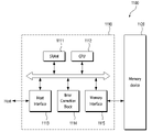
도 1은 본 기술의 실시예에 따른 반도체 메모리 장치의 구성을 개략적으로 도시한 블록도이다.
도 2는 본 기술의 실시예에 따른 반도체 메모리 장치의 메모리 블록 일부를 도시한 회로도이다.
도 3은 본 기술의 실시예에 따른 반도체 메모리 장치를 개략적으로 도시한 사시도이다.
도 4는 본 기술의 실시예에 따른 반도체 메모리 장치를 도시한 단면도이다.
도 5는 도 4에 도시된 'A'영역을 확대하여 도시한 단면도이다.
도 6은 본 기술의 실시예에 따른 반도체 메모리 장치의 변형예를 도시한 단면도로서, 도 4에 도시된 'A'영역에 대응하는 단면도이다.
도 7a 내지 도 7e는 본 기술의 실시예에 따른 반도체 메모리 장치의 제조방법을 도시한 단면도이다.
도 8은 본 기술의 실시예에 따른 메모리 시스템의 구성을 나타내는 블록도이다.
도 9는 본 기술의 실시예에 따른 컴퓨팅 시스템의 구성을 나타내는 블록도이다.1 is a block diagram schematically illustrating a configuration of a semiconductor memory device according to an embodiment of the present technology.
2 is a circuit diagram illustrating a part of a memory block of a semiconductor memory device according to an embodiment of the present technology.
3 is a perspective view schematically illustrating a semiconductor memory device according to an exemplary embodiment of the present technology.
4 is a cross-sectional view illustrating a semiconductor memory device according to an exemplary embodiment of the present technology.
FIG. 5 is an enlarged cross-sectional view of area 'A' shown in FIG. 4 .
6 is a cross-sectional view illustrating a modified example of a semiconductor memory device according to an embodiment of the present technology, and is a cross-sectional view corresponding to region 'A' shown in FIG. 4 .
7A to 7E are cross-sectional views illustrating a method of manufacturing a semiconductor memory device according to an exemplary embodiment of the present technology.
8 is a block diagram illustrating a configuration of a memory system according to an embodiment of the present technology.
9 is a block diagram illustrating a configuration of a computing system according to an embodiment of the present technology.
본 기술의 이점 및 특징, 그리고 그것들을 달성하는 방법은 첨부되는 도면과 함께 상세하게 후술되어 있는 실시예들을 참조하면 명확해질 것이다. 그러나 본 기술은 이하에서 개시되는 실시예들에 한정되는 것이 아니라 서로 다른 다양한 형태로 구현될 것이며, 단지 본 실시예들은 본 기술의 개시가 완전하도록 하며, 본 기술이 속하는 기술분야에서 통상의 지식을 가진 자에게 발명의 범주를 완전하게 알려주기 위해 제공되는 것이며, 본 기술은 청구항의 범주에 의해 정의될 뿐이다. 도면에서 층 및 영역들의 크기 및 상대적인 크기는 설명의 명료성을 위해 과장된 것일 수 있다. 명세서 전체에 걸쳐 동일 참조 부호는 동일 구성 요소를 지칭한다.Advantages and features of the present technology and methods of achieving them will become apparent with reference to the embodiments described below in detail in conjunction with the accompanying drawings. However, the present technology is not limited to the embodiments disclosed below, but will be implemented in various different forms, and only the present embodiments allow the disclosure of the present technology to be complete, and common knowledge in the technical field to which the present technology belongs It is provided to fully inform the possessor of the scope of the invention, and the present technology is only defined by the scope of the claims. Sizes and relative sizes of layers and regions in the drawings may be exaggerated for clarity of description. Like reference numerals refer to like elements throughout.
후술하는 본 기술의 실시예는 개선된 신뢰성을 갖는 반도체 메모리 장치 및 그 제조방법을 제공하기 위한 것이다. 보다 구체적으로, 반도체 메모리 장치가 고온 환경에 지속적으로 노출되는 상황에서 프로그램된 데이터가 손실되는 것을 방지하여 데이터 유지(retention) 특성이 향상된 반도체 메모리 장치 및 그 제조방법을 제공하기 위한 것이다. 여기서, 반도체 메모리 장치는 전하 트랩(Charge trap) 기반의 3차원 구조를 갖는 비휘발성 메모리 장치 예컨대, 3차원 낸드(3D NAND)를 포함할 수 있다.An embodiment of the present technology, which will be described later, is intended to provide a semiconductor memory device having improved reliability and a method of manufacturing the same. More specifically, it is an object of the present invention to provide a semiconductor memory device having improved data retention characteristics by preventing loss of programmed data in a situation in which the semiconductor memory device is continuously exposed to a high temperature environment, and a method for manufacturing the same. Here, the semiconductor memory device may include a non-volatile memory device having a three-dimensional structure based on a charge trap, for example, a three-dimensional NAND (3D NAND).
참고로, 차량용 반도체 메모리 장치의 경우 메모리셀들에 데이터가 프로그램된 상태에서 수번의 IR-리플로우(IR-Reflow)를 진행해야 한다. 여기서, IR-리플로우는 적외선 열처리를 통해 고온에서 수행되는 반도체 패키징 공정을 지칭할 수 있다. IR-리플로우는 고온 환경에서 수행되기 때문에 프로그램된 데이터가 손실될 수 있다. 예를 들어, 전하 트랩 기반의 반도체 메모리 장치의 경우 고온 환경에 지속적으로 노출되게 되면, 트랩된 전하의 열 방출(thermal emission)로 인해 프로그램된 데이터의 손실이 발생하여 데이터 유지 특성이 열화될 수 있다. 따라서, 고온 환경으로 인해 프로그램된 데이터가 손실되어 반도체 메모리 장치의 신뢰성이 저하되는 것을 반드시 방지할 필요가 있다. For reference, in the case of a semiconductor memory device for a vehicle, it is necessary to perform IR-reflow several times in a state in which data is programmed in the memory cells. Here, IR-reflow may refer to a semiconductor packaging process performed at a high temperature through infrared heat treatment. Because IR-reflow is performed in a high temperature environment, programmed data may be lost. For example, in the case of a charge trap-based semiconductor memory device, when continuously exposed to a high temperature environment, loss of programmed data may occur due to thermal emission of the trapped charge, thereby deteriorating data retention characteristics. . Therefore, it is necessary to prevent the loss of the programmed data due to the high temperature environment, thereby reducing the reliability of the semiconductor memory device.
이를 위해, 후술하는 본 기술의 실시예에 따른 반도체 메모리 장치 및 그 제조방법은 데이터(또는 전하)가 저장되는 메모리막 및 메모리막에 접하는 구조물에 불소 이온을 주입하여 모바일 이온(mobile ion)의 움직임을 억제하고, IR-리플로우와 같은 고온 환경에서 프로그램된 데이터가 손실되는 것을 방지할 수 있는 방법을 제공한다. To this end, in a semiconductor memory device and a method for manufacturing the same according to an embodiment of the present technology, which will be described later, movement of mobile ions by implanting fluorine ions into a memory film in which data (or electric charge) is stored and a structure in contact with the memory film. and provides a method to prevent loss of programmed data in high-temperature environments such as IR-reflow.
이하, 도면을 참조하여 본 기술의 실시예에 따른 반도체 메모리 장치에 대해 상세히 설명하기로 한다. 이하의 설명에서 제1방향(D1), 제2방향(D2) 및 제3방향(D3)은 서로 교차하는 방향일 수 있다. 예를들어, XYZ좌표계에서 제1방향(D1), 제2방향(D2) 및 제3방향(D3) 각각은 X축 방향, Y축 방향 및 Z축 방향일 수 있다.Hereinafter, a semiconductor memory device according to an embodiment of the present technology will be described in detail with reference to the drawings. In the following description, the first direction D1 , the second direction D2 , and the third direction D3 may cross each other. For example, each of the first direction D1 , the second direction D2 , and the third direction D3 in the XYZ coordinate system may be an X-axis direction, a Y-axis direction, and a Z-axis direction.
도 1은 본 기술의 실시예에 따른 반도체 메모리 장치의 구성을 개략적으로 도시한 블록도이다.1 is a block diagram schematically illustrating a configuration of a semiconductor memory device according to an embodiment of the present technology.
도 1에 도시된 바와 같이, 반도체 메모리 장치(10)는 주변회로(peripheral circuit, PC) 및 메모리 셀 어레이(memory cell array, 20)를 포함할 수 있다. 1 , the
주변회로(PC)는 메모리 셀 어레이(20)에 데이터를 저장하기 위한 프로그램 동작(program operation), 메모리 셀 어레이(20)에 저장된 데이터를 출력하기 위한 리드 동작(read operation) 및 메모리 셀 어레이(20)에 저장된 데이터를 소거하기 위한 소거 동작(erase operation)을 제어하도록 구성될 수 있다. 예를 들어, 주변회로(PC)는 전압생성부(Voltage Generator, 31), 로우디코더(Row decoder, 33), 제어회로(Control circuit, 35) 및 페이지 버퍼 그룹(Page Buffer Group, 37)을 포함할 수 있다.The peripheral circuit PC includes a program operation for storing data in the
메모리 셀 어레이(20)는 복수의 메모리 블록들을 포함할 수 있다. 메모리 셀 어레이(20)는 워드라인들(WL)을 통해 로우디코더(33)에 연결될 수 있고, 비트라인들(BL)을 통해 페이지 버퍼 그룹(37)에 연결될 수 있다.The
제어회로(35)은 커맨드(CMD) 및 어드레스(ADD)에 응답하여 주변회로(PC)를 제어할 수 있다.The
전압생성부(31)는 제어회로(35)의 제어에 응답하여 프로그램 동작, 리드 동작 및 소거 동작에 사용되는 프리-소거전압(Pre-erase voltage), 소거전압(Erase voltage), 접지전압(Ground voltage), 프로그램전압(Program voltage), 검증전압(Verification voltage), 패스전압(Pass voltage), 리드전압(Lead voltage) 등의 다양한 동작전압들을 생성할 수 있다.The
로우디코더(33)는 제어회로(35)의 제어에 응답하여 메모리 블록을 선택할 수 있다. 로우디코더(33)는 선택된 메모리 블록에 연결된 워드라인들(WL)에 동작 전압들을 인가하도록 구성될 수 있다.The
페이지 버퍼 그룹(37)은 비트라인들(BL)을 통해 메모리 셀 어레이(20)에 연결될 수 있다. 페이지 버퍼 그룹(37)은 제어회로(35)의 제어에 응답하여 프로그램 동작시 입출력 회로(미도시)로부터 수신되는 데이터를 임시 저장할 수 있다. 페이지 버퍼 그룹(37)은 제어회로(35)의 제어에 응답하여 리드 동작 또는 검증 동작 시, 비트 라인들(BL)의 전압 또는 전류를 센싱할 수 있다. 페이지 버퍼 그룹(37)은 제어회로(35)의 제어에 응답하여 비트라인들(BL)을 선택할 수 있다.The
구조적으로, 메모리 셀 어레이(20)는 주변회로(PC)와 나란히 배치되거나, 또는 메모리 셀 어레이(20)가 주변회로(PC)의 일부에 중첩될 수 있다.Structurally, the
도 2는 본 기술의 실시예에 따른 반도체 메모리 장치의 메모리 블록 일부를 도시한 회로도이다.2 is a circuit diagram illustrating a part of a memory block of a semiconductor memory device according to an embodiment of the present technology.
도 2에 도시된 바와 같이, 메모리 블록은 소스막(SL) 및 복수의 워드라인들(WL1~WLn)에 공통으로 연결된 복수의 셀스트링들(CS1, CS2)을 포함할 수 있다. 그리고, 복수의 셀스트링들(CS1, CS2)은 복수의 비트라인들(BL)에 연결될 수 있다.As shown in FIG. 2 , the memory block may include a source layer SL and a plurality of cell strings CS1 and CS2 commonly connected to a plurality of word lines WL1 to WLn. In addition, the plurality of cell strings CS1 and CS2 may be connected to the plurality of bit lines BL.
복수의 셀스트링들(CS1, CS2) 각각은 소스막(SL)에 연결된 하나 이상의 소스 선택 트랜지스터(SST), 비트라인(BL)에 연결된 하나 이상의 드레인 선택 트랜지스터(DST) 및 소스 선택 트랜지스터(SST)와 드레인 선택 트랜지스터(DST) 사이에 직렬로 연결된 복수의 메모리셀들(MC1~MCn)을 포함할 수 있다.Each of the plurality of cell strings CS1 and CS2 includes one or more source select transistors SST connected to the source layer SL, one or more drain select transistors DST and one or more source select transistors SST connected to the bit line BL. and a plurality of memory cells MC1 to MCn connected in series between the and drain select transistor DST.
복수의 메모리셀들(MC1~MCn)의 게이트들은 제3방향(D3)으로 서로 이격되어 적층된 복수의 워드라인들(WL1~WLn)에 각각 연결될 수 있다. 복수의 워드라인들(WL1~WLn)은 소스 선택라인(SSL)과 2개 이상의 드레인 선택라인들(DSL1, DSL2) 사이에 배치될 수 있다. 2개 이상의 드레인 선택라인들(DSL1, DSL2)은 동일레벨에서 서로 이격될 수 있다.Gates of the plurality of memory cells MC1 to MCn may be respectively connected to a plurality of word lines WL1 to WLn that are spaced apart from each other in the third direction D3 and stacked. The plurality of word lines WL1 to WLn may be disposed between the source select line SSL and the two or more drain select lines DSL1 and DSL2 . The two or more drain selection lines DSL1 and DSL2 may be spaced apart from each other at the same level.
한편, 본 실시예에서는 복수의 셀스트링들(CS1, CS2)이 하나의 소스 선택라인(SSL)에 연결된 경우를 예시하였으나, 이에 한정되지 않는다. 변형예로서, 소스 선택라인(SSL)은 동일레벨에서 서로 이격된 복수의 도전라인으로 구성되거나, 또는 제3방향(D3)으로 서로 이격되어 적층된 복수의 도전라인으로 구성될 수도 있다. Meanwhile, in the present embodiment, the case in which the plurality of cell strings CS1 and CS2 are connected to one source selection line SSL has been exemplified, but the present invention is not limited thereto. As a modification, the source selection line SSL may be formed of a plurality of conductive lines spaced apart from each other at the same level, or may include a plurality of stacked conductive lines spaced apart from each other in the third direction D3 .
소스 선택 트랜지스터(SST)의 게이트는 소스 선택라인(SSL)에 연결될 수 있다. 드레인 선택 트랜지스터(DST)의 게이트는 드레인 선택 트랜지스터(DST)의 게이트에 대응하는 드레인 선택라인에 연결될 수 있다.A gate of the source select transistor SST may be connected to the source select line SSL. A gate of the drain select transistor DST may be connected to a drain select line corresponding to the gate of the drain select transistor DST.
소스막(SL)은 소스 선택 트랜지스터(SST)의 소스에 연결될 수 있다. 드레인 선택 트랜지스터(DST)의 드레인은 드레인 선택 트랜지스터(DST)의 드레인에 대응하는 비트라인(BL)에 연결될 수 있다.The source layer SL may be connected to the source of the source select transistor SST. A drain of the drain select transistor DST may be connected to a bit line BL corresponding to a drain of the drain select transistor DST.
복수의 셀스트링들(CS1, CS2)은 2개 이상의 드레인 선택라인들(DSL1, DSL2)에 각각 연결된 스트링 그룹들로 구분될 수 있다. 동일한 워드라인 및 동일한 비트라인에 연결된 셀스트링들은 서로 다른 드레인 선택라인들에 의해 독립적으로 제어될 수 있다. 또한, 동일한 드레인 선택라인에 연결된 셀스트링들은 서로 다른 비트라인들에 의해 독립적으로 제어될 수 있다. 예를 들어, 2개 이상의 드레인 선택라인들(DSL1, DSL2)은 제1드레인 선택라인(DSL1) 및 제2드레인 선택라인(DSL2)을 포함할 수 있다. 복수의 셀스트링들(CS1, CS2)은 제1드레인 선택라인(DSL1)에 연결된 제1스트링 그룹의 제1셀스트링(CS1) 및 제2드레인 선택라인(DSL2)에 연결된 제2스트링 그룹의 제2셀스트링(CS2)을 포함할 수 있다.The plurality of cell strings CS1 and CS2 may be divided into string groups respectively connected to two or more drain selection lines DSL1 and DSL2. Cell strings connected to the same word line and the same bit line may be independently controlled by different drain select lines. In addition, cell strings connected to the same drain select line may be independently controlled by different bit lines. For example, the two or more drain select lines DSL1 and DSL2 may include a first drain select line DSL1 and a second drain select line DSL2 . The plurality of cell strings CS1 and CS2 include the first cell string CS1 of the first string group connected to the first drain selection line DSL1 and the second string group connected to the second drain selection line DSL2. It may include two cell strings (CS2).
도 3은 본 기술의 실시예에 따른 반도체 메모리 장치를 개략적으로 도시한 사시도이다. 3 is a perspective view schematically illustrating a semiconductor memory device according to an exemplary embodiment of the present technology.
도 3에 도시된 바와 같이, 반도체 메모리 장치(10)는 기판(SUB) 상에 배치된 주변회로(PC) 및 주변회로(PC)에 중첩된 게이트적층체들(GST)을 포함할 수 있다.As shown in FIG. 3 , the
게이트적층체들(GST) 각각은 소스 선택라인(SSL), 복수의 워드라인들(WL1~WLn) 및 제1슬릿(S1)에 의해 동일레벨에서 서로 분리된 2개 이상의 드레인 선택라인들(DSL1, DSL2)을 포함할 수 있다. Each of the gate stacked bodies GST is a source select line SSL, a plurality of word lines WL1 to WLn, and two or more drain select lines DSL1 separated from each other at the same level by a first slit S1 . , DSL2).
소스 선택라인(SSL) 및 복수의 워드라인들(WL1~WLn)은 제1방향(D1) 및 제2방향(D2)으로 확장될 수 있고, 기판(SUB)의 상면에 나란한 평판형태로 형성될 수 있다. The source selection line SSL and the plurality of word lines WL1 to WLn may extend in the first direction D1 and the second direction D2 and may be formed in a flat plate shape parallel to the upper surface of the substrate SUB. can
복수의 워드라인들(WL1~WLn)은 제3방향(D3)으로 서로 이격되어 적층될 수 있다. 복수의 워드라인들(WL1~WLn)은 2개 이상의 드레인 선택라인들(DSL1, DSL2)과 소스 선택라인(SSL) 사이에 배치될 수 있다.The plurality of word lines WL1 to WLn may be stacked while being spaced apart from each other in the third direction D3 . The plurality of word lines WL1 to WLn may be disposed between two or more drain select lines DSL1 and DSL2 and the source select line SSL.
게이트적층체들(GST)은 제2슬릿(S2)에 의해 서로 분리될 수 있다. 제1슬릿(S1)은 제2슬릿(S2)보다 제3방향(D3)으로 짧게 형성되고, 복수의 워드라인들(WL1~WLn)에 중첩될 수 있다.The gate stacked bodies GST may be separated from each other by the second slit S2 . The first slit S1 may be shorter than the second slit S2 in the third direction D3 and overlap the plurality of word lines WL1 to WLn.
제1슬릿(S1) 및 제2슬릿(S2) 각각은 제2방향으로 직선형, 지그재그형 또는 웨이브형으로 연장될 수 있다. 제1슬릿(S1) 및 제2슬릿(S2) 각각의 폭은 디자인 룰에 따라 다양하게 변경될 수 있다.Each of the first slit S1 and the second slit S2 may extend in a straight line, a zigzag shape, or a wave shape in the second direction. The width of each of the first slit S1 and the second slit S2 may be variously changed according to a design rule.
소스 선택라인(SSL)은 2개 이상의 드레인 선택라인들(DSL1, DSL2)보다 주변회로(PC)에 더 가깝게 배치될 수 있다. 반도체 메모리 장치(10)는 게이트적층체들(GST)과 주변회로(PC) 사이에 배치된 소스막(SL) 및 소스막(SL)보다 주변회로(PC)로부터 더 멀리 이격된 복수의 비트라인들(BL)을 포함할 수 있다. 게이트적층체들(GST)은 복수의 비트라인들(BL)과 소스막(SL) 사이에 배치될 수 있다.The source select line SSL may be disposed closer to the peripheral circuit PC than the two or more drain select lines DSL1 and DSL2 . The
복수의 비트라인들(BL)은 다양한 도전물질 예컨대, 도프드 반도체막, 금속막, 금속합금막 등으로 형성될 수 있다. 소스막(SL)은 도프드 반도체막을 포함할 수 있다. 예를 들어, 소스막(SL)은 n형 도프드 실리콘막을 포함할 수 있다.The plurality of bit lines BL may be formed of various conductive materials, for example, a doped semiconductor layer, a metal layer, a metal alloy layer, or the like. The source layer SL may include a doped semiconductor layer. For example, the source layer SL may include an n-type doped silicon layer.
한편, 도면에 도시하지는 않았으나, 주변회로(PC)는 다양한 구조의 인터커넥션들을 통해 복수의 비트라인들(BL), 소스막(SL), 및 복수의 워드라인들(WL1 내지 WLn)에 전기적으로 연결될 수 있다.Meanwhile, although not shown in the drawings, the peripheral circuit PC is electrically connected to the plurality of bit lines BL, the source layer SL, and the plurality of word lines WL1 to WLn through interconnections having various structures. can be connected
도 4는 본 기술의 실시예에 따른 반도체 메모리 장치를 도시한 단면도이고, 도 5는 도 4에 도시된 'A'영역을 확대하여 도시한 단면도이다. 그리고, 도 6은 본 기술의 실시예에 따른 반도체 메모리 장치의 변형예를 도시한 단면도로서, 도 4에 도시된 'A'영역에 대응하는 단면도이다. 4 is a cross-sectional view illustrating a semiconductor memory device according to an exemplary embodiment of the present technology, and FIG. 5 is an enlarged cross-sectional view of region 'A' of FIG. 4 . 6 is a cross-sectional view illustrating a modified example of a semiconductor memory device according to an embodiment of the present technology, and is a cross-sectional view corresponding to region 'A' shown in FIG. 4 .
도 4 및 도 5에 도시된 바와 같이, 본 기술의 실시예에 따른 반도체 메모리 장치는 소스막(SL), 소스막(SL) 상에 형성된 복수의 게이트적층체들(GST), 게이트적층체들(GST) 사이에 형성된 슬릿구조물들(110) 및 게이트적층체(GST)를 관통하는 복수의 채널구조물들(CH)을 포함할 수 있다. 4 and 5 , in the semiconductor memory device according to an embodiment of the present technology, a source layer SL, a plurality of gate stacked bodies GST formed on the source layer SL, and gate stacked bodies are included. The
소스막(SL)은 게이트적층체들(GST)과 중첩될 수 있고, 제1방향(D1) 및 제2방향(D2)으로 연장된 평판형상을 가질 수 있다. 소스막(SL)은 제1소스막(SL1), 제3소스막(SL3) 및 제2소스막(SL2)이 순차적으로 적층된 구조를 가질 수 있다. 즉, 소스막(SL)은 제1소스막(SL1)과 제2소스막(SL2) 사이에 제3소스막(SL3)이 삽입된 구조를 가질 수 있다. 여기서, 제3소스막(SL3)은 채널구조물들(CH) 각각의 채널막(140)에 전기적으로 연결될 수 있다. The source layer SL may overlap the gate stacked bodies GST and may have a flat plate shape extending in the first direction D1 and the second direction D2 . The source layer SL may have a structure in which a first source layer SL1 , a third source layer SL3 , and a second source layer SL2 are sequentially stacked. That is, the source layer SL may have a structure in which the third source layer SL3 is inserted between the first source layer SL1 and the second source layer SL2 . Here, the third source layer SL3 may be electrically connected to the
게이트적층체들(GST) 각각은 복수의 슬릿구조물들(110)에 의해 분리될 수 있다. 구체적으로, 제1방향(D1)으로 게이트적층체들(GST) 각각의 양측벽에 슬릿구조물들(110)이 위치할 수 있다. 슬릿구조물들(110)에 의해 분리된 게이트적층체들(GST) 각각은 하나의 메모리 블록에 대응할 수 있다. 게이트적층체들(GST) 하부에는 소스막(SL)이 위치할 수 있고, 게이트적층체들(GST) 상부에는 복수의 비트라인들(미도시, 도 3 참조)이 위치할 수 있다. 따라서, 소스막(SL), 게이트적층체들(GST) 및 복수의 비트라인들은 서로 중첩될 수 있다. Each of the gate stacked structures GST may be separated by a plurality of
한편, 본 실시예에서는 게이트적층체들(GST) 하부에 소스막(SL)이 위치하고, 게이트적층체들(GST) 상부에 비트라인들이 위치하는 경우를 예시하였으나, 이에 한정되지 않는다. 변형예로서, 게이트적층체들(GST) 하부에 비트라인들이 위치하고, 게이트적층체들(GST) 상부에 소스막(SL)이 위치할 수도 있다.Meanwhile, in the present embodiment, the case where the source layer SL is positioned under the gate stacks GST and the bit lines are positioned over the gate stacks GST is exemplified, but the present invention is not limited thereto. As a modification, the bit lines may be positioned under the gate stacked structures GST, and the source layer SL may be positioned over the gate stacked bodies GST.
또한, 본 실시예에서는 제3방향(D3)으로 게이트적층체(GST)가 1단으로 구성된 경우를 예시하였으나, 이에 한정되지 않는다. 변형예로서, 제3방향(D3)으로 둘 이상의 게이트적층체(GST)가 적층된 구조를 가질 수도 있다. In addition, although the case in which the gate stacked body GST is configured in one stage in the third direction D3 is exemplified in the present embodiment, the present invention is not limited thereto. As a modification, it may have a structure in which two or more gate stacked bodies GST are stacked in the third direction D3 .
슬릿구조물들(110) 각각은 도 3에 도시된 제2슬릿(S2)에 대응하는 것일 수 있다. 슬릿구조물들(110) 각각은 제2방향(D2)으로 연장된 라인타입의 패턴일 수 있다. 이때, 슬릿구조물들(110) 각각은 제2방향(D2)으로 직선형, 지그재그형 또는 웨이브형으로 연장될 수 있다. 제3방향(D3)으로 슬릿구조물(110)의 하단부는 소스막(SL) 내부로 확장된 형태를 가질 수 있다. 예를 들어, 슬릿구조물(110)의 저면은 제3소스막(SL3)에 접할 수 있다. Each of the
슬릿구조물들(110) 각각은 제2방향(D2)으로 연장된 라인타입의 슬릿트렌치(112), 제1방향(D1)으로 슬릿트렌치(112)의 양측벽에 형성된 슬릿스페이서(114) 및 슬릿트렌치(112)를 갭필하는 슬릿막(116)을 포함할 수 있다. 슬릿스페이서(114)는 절연물질을 포함할 수 있고, 슬릿막(116)은 도전물질을 포함할 수 있다. Each of the
한편, 본 실시예에서는 슬릿막(116)이 도전물질을 포함하는 경우를 예시하였으나, 이에 한정되지 않는다. 변형예로서, 슬릿막(116)은 절연물질을 포함할 수도 있다. Meanwhile, in the present embodiment, the case in which the
게이트적층체들(GST) 각각은 층간절연막(102)과 게이트도전막(104)이 복수회 교번 적층된 적층구조물일 수 있다. 게이트적층체(GST)에서 최하층 및 최상층에는 각각 층간절연막(102)이 위치할 수 있다. 게이트적층체(GST)에서 최상층에 위치하는 층간절연막(102)은 나머지 층간절연막(102)들보다 상대적으로 더 두꺼운 두께를 가질 수 있다. 그리고, 층간절연막(102) 및 게이트도전막(104) 각각은 제1방향(D1) 및 제2방향(D2)으로 연장된 평판형상을 가질 수 있다. Each of the gate stacked bodies GST may be a stacked structure in which an
층간절연막(102)은 산화막, 질화막 및 산질화막으로 이루어진 그룹으로부터 선택된 어느 하나의 절연막을 포함할 수 있다. 여기서, 층간절연막(102)은 고온 환경에서 데이터 유지 특성을 향상시키기 위해 막내 복수의 불소 이온이 함유된 절연막일 수 있다. 이때, 불소 이온은 음전하를 가질 수 있다. 일례로, 층간절연막(102)은 막내 음전하를 갖는 복수의 불소 이온이 함유된 실리콘산화막으로 형성할 수 있다. The interlayer insulating
층간절연막(102)에 함유된 불소 이온은 층간절연막(102)의 내부 및 표면에 생성된 결함 예컨대, 공공(vacancy) 또는 댕글링 본드(Dangling bond)을 치유하여 결함에 기인한 트랩을 억제하는 역할을 수행할 수 있다. 예를 들어, 층간절연막(102)을 실리콘산화막으로 형성한 경우, 불소 이온은 산소 공공(oxygen vacancy) 또는 실리콘 댕글링 본드와 결합하여 실리콘-불소 결합(Si-F bond)을 형성할 수 있다. 이를 통해, 층간절연막(102)의 내부 및 표면에 생성된 결함을 치유할 수 있고, 결함에 기인한 트랩을 억제할 수 있다. 참고로, 결함을 치유하여 결함에 기인한 트랩을 억제하는 것은 트랩이 전하를 포획하는 사이트(site)로 작용하지 못하도록 비활성화시키는 것을 의미할 수 있다. Fluorine ions contained in the
또한, 층간절연막(102)에 함유된 불소 이온은 양전하를 갖는 모바일 이온에 의하여 메모리셀 문턱전압의 이상 변동을 방지하는 역할을 수행할 수 있다. 구체적으로, 프로그램 동작 및 소거 동작을 반복하는 과정에서 층간절연막(102) 내의 모바일 이온들이 메모리셀의 메모리막(130) 주변 및 채널막(140) 주변에 축적되어 메모리셀의 문턱전압 분포가 변동(또는 쉬프트)될 수 있다. 이때, 층간절연막(102)에 함유된 불소 이온이 모바일 이온의 이동을 억제하여 모바일 이온이 메모리셀들 각각의 메모리막(130) 주변 및 채널막(140) 주변에 축적되는 것을 방지할 수 있다. 아울러, 메모리셀들 각각의 메모리막(130) 주변 및 채널막(140) 주변에 모바일 이온이 축적되더라도, 음전하를 갖는 불소 이온이 양전하를 갖는 모바일 이온을 전기적으로 중화시켜 메모리셀의 문턱전압 분포가 변동되는 것을 방지할 수 있다. In addition, the fluorine ions contained in the
게이트도전막(104)은 금속이 함유된 도전막을 포함할 수 있다. 일례로, 게이트도전막(104)은 텅스텐막(W layer)으로 형성할 수 있다. 다른 일례로, 게이트도전막(104)은 티타늄질화막(TiN layer)과 텅스텐막(W layer)이 적층된 적층막으로 형성할 수도 있다. 여기서, 티타늄질화막은 텅스텐의 확산을 방지하는 장벽막으로 작용할 수 있다.The gate
게이트적층체들(GST) 각각에서 적어도 최하층에 위치하는 게이트도전막(104)은 소스 선택 트랜지스터(SST, 도 2 참조)의 게이트 및 소스 선택라인(SSL, 도 2 및 도 3 참조)으로 작용할 수 있다. The gate
한편, 본 실시예에서는 소스 선택 트랜지스터의 게이트 및 소스 선택라인으로 작용하는 게이트도전막(104)이 단층으로 형성된 경우를 예시하였으나, 이에 한정되지 않는다. 변형예로서, 게이트적층체(GST)에서 최하층에 위치하는 게이트도전막(104)을 포함하여 게이트적층체(GST)의 하단부에 위치하는 수개의 게이트도전막(104)들을 소스 선택 트랜지스터의 게이트 및 소스 선택라인으로 사용할 수 있다. Meanwhile, in the present embodiment, the case in which the gate
또한, 본 실시예에서 게이트적층체들(GST) 각각은 소스 선택라인으로 작용하는 최하층 게이트도전막(104)이 동일레벨에 하나의 패턴으로 형성된 경우를 예시하였으나, 이에 한정되지 않는다. 변형예로서, 게이트적층체들(GST) 각각은 소스 선택라인으로 작용하는 게이트도전막(104)이 동일레벨에서 상호 이격된 적어도 2개 이상의 패턴으로 구성될 수도 있다. In addition, in the present embodiment, the case where the lowermost gate
게이트적층체들(GST) 각각에서 적어도 최상층에 위치하는 게이트도전막(104)은 드레인 선택 트랜지스터(DST, 도 2 참조)의 게이트 및 드레인 선택라인(DSL1, DSL2, 도 2 및 도 3 참조)으로 작용할 수 있다. 게이트적층체(GST)에서 최상층에 위치하는 게이트도전막(104)은 적어도 하나 이상의 분리막(106)에 의해 동일레벨에서 상호 이격된 적어도 2개 이상의 패턴으로 분리될 수 있다. 여기서, 분리막(106)은 도 3에 도시된 제1슬릿(S1)에 대응하는 것일 수 있다. 따라서, 제1방향(D1)으로 분리막(106)의 일측 및 타측에 위치하는 게이트도전막(104)은 도 3에 도시된 제1드레인 선택라인(DSL1) 및 제2드레인 선택라인(DSL2)에 대응하는 것일 수 있다. 분리막(106)은 산화막, 질화막 및 산질화막으로 이루어진 그룹으로부터 선택된 어느 하나의 절연막을 포함할 수 있다. 일례로, 분리막(106)은 산화막으로 형성될 수 있다. The gate
한편, 본 실시예에서는 드레인 선택 트랜지스터의 게이트 및 드레인 선택라인으로 작용하는 게이트도전막(104)이 단층으로 형성된 경우를 예시하였으나, 이에 한정되지 않는다. 변형예로서, 게이트적층체(GST)에서 최상층에 위치하는 게이트도전막(104)을 포함하여 게이트적층체(GST)의 상단부에 위치하는 수개의 게이트도전막(104)들을 드레인 선택 트랜지스터의 게이트 및 드레인 선택라인으로 사용할 수 있다. Meanwhile, in the present embodiment, the case in which the gate
게이트적층체들(GST) 각각에서 소스 선택라인으로 작용하는 게이트도전막(104)과 드레인 선택라인으로 작용하는 게이트도전막(104) 사이에 위치하는 게이트도전막(104)들 각각은 메모리 셀 트랜지스터의 게이트 및 워드라인으로 작용할 수 있다. 따라서, 게이트적층체(GST)에서 최상층 게이트도전막(104)과 최하층 게이트도전막(104) 사이에 위치하는 게이트도전막(104)들은 도 3에 도시된 복수의 워드라인들(WL1~WLn)에 대응하는 것일 수 있다. Each of the gate
복수의 채널구조물들(CH)은 게이트적층체(GST)에서 매트릭스 구조로 배열될 수 있다. 채널구조물들(CH) 각각의 평면형상은 삼각형 이상의 다각형, 원형 또는 타원형일 수 있다. 채널구조물들(CH) 각각은 제3방향(D3)으로 연장된 기둥 형상(Pillar shape)을 가질 수 있고, 고종횡비(High aspect ratio)를 갖는 구조물일 수 있다. 따라서, 채널구조물들(CH) 각각은 제3방향(D3)으로 상단부에서 하단부로 갈수록 점차 선폭이 감소하는 사다리꼴 타입(trapezoid type)의 단면형상을 가질 수 있다.The plurality of channel structures CH may be arranged in a matrix structure in the gate stacked body GST. A planar shape of each of the channel structures CH may be a polygonal shape of a triangle or more, a circular shape, or an elliptical shape. Each of the channel structures CH may have a pillar shape extending in the third direction D3 and may be a structure having a high aspect ratio. Accordingly, each of the channel structures CH may have a trapezoid type cross-sectional shape in which the line width gradually decreases from the upper end to the lower end in the third direction D3 .
채널구조물들(CH) 각각은 게이트적층체(GST)를 관통하고, 하단부가 소스막(SL) 내부로 연장된 형태를 가질 수 있다. 구체적으로, 채널구조물(CH)의 하단부는 제1소스막(SL1) 및 제3소스막(SL3)을 관통하고, 저면이 제1소스막(SL1) 내부에 위치할 수 있다. 소스막(SL) 내부로 연장된 채널구조물(CH)의 하단부를 통해 채널구조물들(CH) 각각은 소스막(SL)과 전기적으로 연결될 수 있다. Each of the channel structures CH may pass through the gate stacked body GST and have a lower end extending into the source layer SL. Specifically, the lower end of the channel structure CH may pass through the first source layer SL1 and the third source layer SL3 , and the bottom may be positioned inside the first source layer SL1 . Each of the channel structures CH may be electrically connected to the source layer SL through a lower end of the channel structure CH extending into the source layer SL.
한편, 제3방향(D3)으로 둘 이상의 게이트적층체(GST)가 적층된 구조를 갖는 경우, 채널구조물(CH)도 게이트적층체(GST)와 같이 적층된 구조를 가질 수 있다. 예를 들어, 제3방향(D3)으로 2개의 게이트적층체(GST)가 적층된 구조를 갖는 경우에 각각의 게이트적층체(GST)에 대응하도록 형성된 2개의 채널구조물들(CH)이 제3방향(D3)으로 적층된 구조를 가질 수도 있다. Meanwhile, when two or more gate stacked bodies GST are stacked in the third direction D3 , the channel structure CH may also have a stacked structure like the gate stacked bodies GST. For example, in a case in which two gate stacked structures GST are stacked in the third direction D3, two channel structures CH formed to correspond to each gate stacked structure GST are formed in the third direction. It may have a structure stacked in the direction D3.
채널구조물들(CH) 각각은 게이트적층체(GST)에 형성된 채널홀(120), 채널홀(120) 표면을 따라 형성된 메모리막(130), 게이트적층체(GST)와 메모리막(130) 사이에 삽입된 제1불소함유막(122), 채널홀(120) 표면을 따라 메모리막(130) 상에 형성된 채널막(140), 메모리막(130)과 채널막(140) 사이에 삽입된 제2불소함유막(124), 채널막(140) 상에 형성되어 채널홀(120)을 일부 갭필하는 절연코어(160) 및 절연코어(160) 상에 형성되어 나머지 채널홀(120)을 갭필하는 캡핑막(150)을 포함할 수 있다. 여기서, 메모리막(130)은 블록킹막(132), 전하트랩막(134) 및 터널절연막(136)이 순차적으로 적층된 적층막을 포함할 수 있다. 메모리막(130)에서 블록킹막(132)은 제1불소함유막(122)에 접할 수 있고, 터널절연막(136)은 제2불소함유막(124)에 접할 수 있다.Each of the channel structures CH includes a
절연코어(160)는 게이트적층체(GST)를 관통하고, 하단부가 소스막(SL) 내부로 연장된 기둥 형상을 가질 수 있다. 절연코어(160)는 산화막, 질화막 및 산질화막으로 이루어진 그룹으로부터 선택된 어느 하나의 절연막을 포함할 수 있다. 일례로, 절연코어(160)는 산화막으로 형성할 수 있다. The insulating
캡핑막(150)은 절연코어(160) 상에 위치하고, 기둥 형상을 가질 수 있다. 캡핑막(150)은 드레인 선택 트랜지스터(DST, 도 2 참조)의 소스 또는 드레인으로 작용할 수 있다. 절연코어(160)와 캡핑막(150)이 접하는 계면은 게이트적층체(GST)의 최상층에 위치하는 게이트도전막(104)의 표면에 정렬되거나, 또는 게이트적층체(GST)의 최상층에 위치하는 게이트도전막(104)의 표면보다 상부에 위치할 수 있다. 여기서, 게이트적층체(GST)의 최상층에 위치하는 게이트도전막(104)은 드레인 선택 트랜지스터(DST, 도 2 참조)의 게이트를 지칭할 수 있다. 캡핑막(150)은 채널막(140)과 전기적으로 연결될 수 있다. 캡핑막(150)은 도프드 반도체막을 포함할 수 있다. 일례로, 캡핑막(150))은 n형 도프드 실리콘막으로 형성할 수 있다. The
채널막(140)은 캡핑막(150)의 측면, 절연코어(160)의 측면 및 저면을 감싸는 실린더 형상을 가질 수 있다. 참고로, 실린더 형상은 내부에 공간을 구비하는 기둥에서 상부면이 개방된 형상을 지칭하며, 컵(cup)과 유사한 형상일 수 있다. 채널막(140)은 소스막(SL)과 전기적으로 연결될 수 있다. 채널막(140)은 반도체막을 포함할 수 있다. 예를 들어, 채널막(140)은 실리콘막을 포함할 수 있다.The
한편, 본 실시예에서는 채널막(140)이 캡핑막(150)의 측면을 감싸는 구조를 갖는 경우를 예시하였으나, 이에 한정되지 않는다. 변형예로서, 채널막(140)은 절연코어(160)의 측면 및 저면을 감싸는 실린더 형상을 갖되, 채널막(140)의 상단부가 캡핑막(150)의 저면에 접하는 구조를 가질 수도 있다. Meanwhile, in the present embodiment, the
메모리막(130)에서 터널절연막(136)은 채널막(140)의 측면 및 저면을 감싸는 실린더 형상을 가질 수 있다. 터널절연막(136)은 산화막, 질화막 및 산화질화막으로 이루어진 그룹으로부터 선택된 어느 하나를 포함할 수 있다. 예를 들어, 터널절연막(136)은 산화막 또는 막내 복수의 불소 이온이 함유된 산화막으로 형성할 수 있다. 일례로, 터널절연막(136)은 실리콘산화막 또는 막내 복수의 불소 이온이 함유된 실리콘산화막으로 형성할 수 있다. In the
한편, 변형예로서, 터널절연막(136)은 질소가 도핑된 산화막 즉, 산질화막 또는 막내 복수의 불소 이온이 함유된 산질화막으로 형성할 수 있다. 산질화막에서 질소 성분은 산화막의 전위장벽 높이를 조절하는 역할을 수행할 수 있다. 이는, 터널절연막(136)의 전위장벽 높이를 밴드갭 엔지니어링(bandgap engineering)을 통해 전도대(conduction band)의 가장자리에 존재하는 트랩에서의 전자 방출에 기인한 메모리셀의 문턱전압 이상 변동을 방지하기 위함이다. 일례로, 터널절연막(136)은 질소가 도핑된 실리콘산화막 즉, 실리콘산질화막 또는 막내 복수의 불소 이온이 함유된 실리콘산질화막으로 형성할 수 있다. Meanwhile, as a modification, the
터널절연막(136)을 막내 복수의 불소 이온이 함유된 산화막 또는 막내 복수의 불소 이온이 함유된 산질화막으로 형성하는 경우, 불소 이온은 터널절연막(136)의 내부 및 표면 그리고, 터널절연막(136)과 접하는 구조물 예컨대, 채널막(140) 및 전하트랩막(134)의 표면에 생성된 결함을 치유하여 결함에 기인한 트랩을 억제하는 역할을 수행할 수 있다. 터널절연막(136)을 막내 복수의 불소 이온이 함유된 산질화막으로 형성하는 경우, 불소 이온은 산질화막에서 질소 성분에 의해 생성된 결함(예컨대, 격자결함)을 치유하여 결함에 기인한 트랩을 억제하는 역할도 수행할 수 있다. When the
특히, 터널절연막(136)에 함유된 불소 이온은 터널절연막(136)과 전하트랩막(134)이 접하는 계면에 생성된 결함을 치유하여 결함에 기인한 트랩을 억제하거나, 트랩 준위를 낮출 수 있다. 구체적으로, 터널절연막(136)과 전하트랩막(134)이 접하는 계면에 생성된 깊은트랩(deep trap)을 얕은트랩(shallow trap)으로 전환시킬 수 있다. 터널절연막(136)과 전하트랩막(134)이 접하는 계면에 생성된 깊은트랩은 동작간 터널절연막(136) 내의 트랩 준위 상호작용으로 인해 트랩 보조 터널링(Trap Assisted Tunneling, TAT)의 발생 확률을 증가시킬 수 있다. 그러나, 본 실시예는 불소 이온을 이용하여 깊은트랩을 얕은트랩으로 전환시킴으로써, 트랩 보조 터널링(TAT)의 발생 확률을 감소시킬 수 있다. In particular, the fluorine ions contained in the
메모리막(130)의 터널절연막(136)과 채널막(140) 사이에 삽입된 제2불소함유막(124)은 데이터 유지 특성 특히, 고온 환경에서의 데이터 유지 특성을 향상시키기 위해 채널막(140)과 터널절연막(136)이 접하는 계면에 생성된 트랩 즉, 표면트랩(interface trap)의 밀도를 감소시키는 역할을 수행할 수 있다. 아울러, 제2불소함유막(124)은 채널막(140)과 터널절연막(136) 사이의 표면트랩 밀도를 감소시켜 누설전류 발생을 억제하고, 트랩 보조 터널링(TAT)의 발생 확률을 감소시키는 역할도 수행할 수 있다. 이를 위해, 제2불소함유막(124)은 채널막(140)과 1종 이상의 동일 원소를 포함하는 불소함유막일 수 있다. 일례로, 채널막(140)이 실리콘막일 경우, 제2불소함유막(124)은 불화실리콘막(SiFx)으로 형성할 수 있다.The second fluorine-containing
후술하겠지만, 터널절연막(136)이 막내 복수의 불소 이온이 함유된 산화막 또는 막내 복수의 불소 이온이 함유된 산질화막인 경우, 터널절연막(136)에 함유된 복수의 불소 이온은 제2불소함유막(124) 형성공정시 터널절연막(136) 내부로 확산된 것일 수 있다. As will be described later, when the
메모리막(130)에서 전하트랩막(134)은 데이터로 작용하는 전하들이 저장되는 공간을 제공하기 위한 것이다. 전하트랩막(134)은 터널절연막(136)의 측면 및 저면을 감싸는 실린더 형상을 가질 수 있다. 전하트랩막(134)은 산화막, 질화막 및 산질화막으로 이루어진 그룹으로부터 선택된 어느 하나를 포함할 수 있다. 일례로, 전하트랩막(134)은 질화막으로 형성할 수 있다. 여기서, 터널절연막(136) 및 후술하는 제2블록킹막(132B) 각각이 막내 복수의 불소 이온을 함유하는 경우, 공정간 터널절연막(136) 및 제2블록킹막(132B) 내부의 불소 이온이 전하트랩막(134) 계면 및 전하트랩막(134) 내부로 확산될 수도 있다. 이를 통해, 전하트랩막(134)의 데이터 유지 특성을 향상시킬 수 있다. In the
메모리막(130)에서 블록킹막(132)은 게이트도전막(104)과 전하트랩막(134) 사이의 전하 터널링을 방지하는 역할을 수행할 수 있다. 블록킹막(132)은 전하트랩막(134)의 측면 및 저면을 감싸는 실린더 형상을 가질 수 있다. 블록킹막(132)은 산화막, 질화막 및 산질화막으로 이루어진 그룹으로부터 선택된 어느 하나의 단층막 또는 둘 이상이 적층된 다층막을 포함할 수 있다. 예를 들어, 블록킹막(132)은 이종 산화막이 적층된 다층막을 포함할 수 있다. 구체적으로, 블록킹막(132)은 제1불소함유막(122)에 접하는 제1블록킹막(132A) 및 전하트랩막(134)에 접하는 제2블록킹막(132B)을 포함할 수 있다. In the
제1블록킹막(132A)은 고유전율을 갖는 절연막을 포함할 수 있다. 예를 들어, 제1블록킹막(132A)은 금속산화막을 포함할 수 있다. 일례로, 제1블록킹막(132A)은 알루미늄산화막(Al2O3) 또는 하프늄산화막(HfO2)으로 형성할 수 있다. The
제2블록킹막(132B)은 반도체산화막을 포함할 수 있다. 구체적으로, 제2블록킹막(132B)은 막내 복수의 불소 이온이 함유된 반도체산화막을 포함할 수 있다. 제2블록킹막(132B)에 함유된 불소 이온은 제2블록킹막(132B) 내부 및 표면 그리고, 제2블로킹막(132B)에 접하는 구조물들 예컨대, 제1블록킹막(132A) 및 전하트랩막(134) 표면에 생성된 결함을 치유하여 결함에 기인한 트랩을 억제하는 역할을 수행할 수 있다. 일례로, 제2블록킹막(132B)은 막내 복수의 불소 이온이 함유된 실리콘산화막으로 형성할 수 있다. The
한편, 본 실시예에서는 블록킹막(132)이 다층막으로 구성된 경우를 예시하였으나, 이에 한정되지 않는다. 변형예로서, 제1블록킹막(132A) 또는 제2블록킹막(132B) 중 어느 하나를 생략할 수도 있다. 일례로, 제2블로킹막(132B)을 생략할 수 있다. Meanwhile, in the present embodiment, the case in which the
메모리막(130)의 블록킹막(132)과 게이트적층체(GST) 사이에 삽입된 제1불소함유막(122)은 데이터 유지 특성 특히, 고온 환경에서의 데이터 유지 특성을 향상시키기 위해 블록킹막(132)과 게이트적층체(GST)가 접하는 계면에 생성된 표면트랩의 밀도를 감소시키는 역할을 수행할 수 있다. 이를 위해, 제1불소함유막(122)은 제1블록킹막(132A)과 1종 이상의 동일 원소를 포함하는 불소함유막일 수 있다. 구체적으로, 제1블록킹막(132A)이 금속산화막일 경우에 제1불소함유막(122)은 금속산불화막(metal oxyfluoride)일 수 있고, 금속산화막 및 금속산화불화막은 각각 동일한 금속 원소를 포함할 수 있다. 일례로, 제1블록킹막(132A)이 알루미늄산화막(Al2O3)일 경우에 제1불소함유막(122)은 알루미늄산불화막(AlOxFy)일 수 있다. The first fluorine-containing
한편, 본 실시예에서는 제1불소함유막(122), 제1블록킹막(132A) 및 제2블록킹막(132B)이 모두 채널홀(120) 내부에 배치되는 구조를 예시하였으나, 이에 한정되지 않는다. 변형예로서, 도 6에 도시된 바와 같이, 제1불소함유막(122) 및 제1블록킹막(132A)은 게이트적층체(GST) 내부에 배치되고, 제2블록킹막(132B)은 채널홀(120) 내부에 배치되는 구조를 가질 수도 있다. 구체적으로, 제2블록킹막(132B)은 채널홀(120) 표면을 따라 형성되어 실린더 형상을 가질 수 있고, 제1불소함유막(122) 및 제1블록킹막(132A)은 층간절연막(102)과 게이트도전막(104) 사이 및 게이트도전막(104)과 제2블록킹막(132B) 사이에 삽입된 형태를 가질 수도 있다. 여기서, 제1불소함유막(122)은 층간절연막(102) 및 제2블록킹막(132B)에 접할 수 있고, 제2블록킹막(132B)은 게이트도전막(104)에 접할 수 있다.Meanwhile, in the present embodiment, the structure in which the first fluorine-containing
한편, 본 실시예에서는 채널구조물(CH)이 제1불소함유막(122) 및 제2불소함유막(124)을 모두 구비하는 경우를 예시하였으나, 이에 한정되지 않는다. 변형예로서, 채널구조물(CH)은 제1불소함유막(122) 또는 제2불소함유막(124) 중 어느 하나만을 구비할 수도 있다. Meanwhile, in the present exemplary embodiment, the channel structure CH includes both the first fluorine-containing
상술한 바와 같이, 본 실시예에 따른 반도체 메모리 장치는 제1불소함유막(122)을 구비함으로써, 게이트적층체(GST)와 블록킹막(132)이 접하는 계면에 생성된 계면트랩 밀도를 감소시킬 수 있다. As described above, the semiconductor memory device according to the present embodiment includes the first fluorine-containing
또한, 제2불소함유막(124)을 구비함으로써, 터널절연막(136)과 채널막(140)이 접하는 계면에서 생성된 계면트랩 밀도를 감소시킬 수 있고, 누설전류 발생을 억제하며, 트랩 보조 터널링(TAT) 발생 확률을 감소시킬 수 있다. In addition, by providing the second fluorine-containing
또한, 불소 이온을 이용하여 메모리막(130) 및 메모리막(130)에 접하는 구조물들에 생성된 결함을 치유하여 결함에 기인한 트랩을 억제함으로써, 고온 환경에서의 데이터 유지 특성을 향상시킬 수 있다. In addition, by using fluorine ions to heal the
또한, 막내 복수의 불소 이온이 함유된 층간절연막(102)을 구비함으로써, 모바일 이온에 의해 메모리셀의 문턱전압 분포가 변동되는 것을 방지할 수 있다. 아울러, 3차원 구조를 갖는 반도체 메모리 장치의 높이에 상관없이 균일한 특성을 구현할 수 있다. In addition, by providing the
따라서, 본 기술의 실시예에 따른 반도체 메모리 장치는 고온 환경에 지속적으로 노출되는 상황에서 프로그램된 데이터가 손실되는 것을 효과적으로 방지할 수 있다. 이를 통해, 반도체 메모리 장치의 신뢰성을 향상시킬 수 있다.Accordingly, the semiconductor memory device according to an embodiment of the present technology can effectively prevent loss of programmed data in a situation in which the semiconductor memory device is continuously exposed to a high temperature environment. Through this, the reliability of the semiconductor memory device may be improved.
도 7a 내지 도 7e는 본 기술의 실시예에 따른 반도체 메모리 장치의 제조방법을 도시한 단면도이다. 설명의 편의를 위해 도 4 및 도 5에 도시된 것과 동일한 구성에 대해서는 동일한 도면부호를 사용하며, 상세한 설명을 생략하기로 한다. 7A to 7E are cross-sectional views illustrating a method of manufacturing a semiconductor memory device according to an exemplary embodiment of the present technology. For convenience of description, the same reference numerals are used for the same components as those shown in FIGS. 4 and 5 , and detailed descriptions thereof will be omitted.
도 7a에 도시된 바와 같이, 소정의 구조물 예컨대, 주변회로(PC, 도 1 및 도 3 참조)가 형성된 기판(미도시) 상에 예비-소스막(200)을 형성한다. 예비-소스막(200)은 제1소스막(SL1), 소스희생막(202) 및 제2소스막(SL2)이 순차적으로 적층된 적층막으로 형성할 수 있다. 예비-소스막(200)은 제1방향(D1) 및 제2방향(D2)으로 연장된 평판형상을 가질 수 있다. 제1소스막(SL1) 및 제2소스막(SL2)은 도프드 반도체막을 포함할 수 있다. 예를 들어, 제1소스막(SL1) 및 제2소스막(SL2)은 각각 n형 도프드 실리콘막으로 형성할 수 있다. 소스희생막(202)은 제1소스막(SL1) 및 제2소스막(SL2)과 식각선택비를 갖는 물질로 형성할 수 있다. 예를 들어, 소스희생막(202)은 산화막, 질화막 및 산질화막으로 이루어진 그룹으로부터 선택된 어느 하나의 단층막 또는 둘 이상이 적층된 다층막으로 형성할 수 있다. 일례로, 소스희생막(202)은 산화막으로 형성할 수 있다. As shown in FIG. 7A , a
다음으로, 예비-소스막(200) 상에 층간절연막(102)과 게이트희생막(204)이 복수회 교번 적층된 적층체(206)를 형성한다. 적층체(206)에서 최하층 및 최상층에는 각각 층간절연막(102)이 위치할 수 있다. 적층체(206)에서 최상층에 위치하는 층간절연막(102)은 상대적으로 더 두꺼운 두께를 갖도록 형성할 수 있다. 게이트희생막(204)은 층간절연막(102)에 대해 식각선택비를 갖는 물질로 형성할 수 있다. 층간절연막(102) 및 게이트희생막(204)은 각각 산화막, 질화막 및 산질화막으로 이루어진 그룹으로부터 선택된 어느 하나를 포함할 수 있다. 이때, 적층체(206)에서 복수의 층간절연막(102) 각각은 막내 복수의 불소 이온이 함유된 절연막으로 형성할 수 있다. 일례로, 층간절연막(102)은 막내 복수의 불소 이온이 함유된 실리콘산화막으로 형성할 수 있고, 게이트희생막(204)은 실리콘질화막으로 형성할 수 있다. Next, a laminate 206 in which an
막내 복수의 불소 이온이 함유된 실리콘산화막은 챔버에 실리콘 소스가스, 산소가스 및 불소가스를 동시에 공급하는 방법으로 형성할 수 있다. 여기서, 반응가스로 삼불화붕소(BF3)와 같은 불소함유가스를 사용하지 않고, 순수 불소가스(F2)를 사용하는 것은 불필요한 불순물이 실리콘산화막에 함유되는 것을 방지하기 위함이다. 참고로, 불소함유가스에서 불소 성분을 제외한 나머지 성분들은 실리콘산화막 내 결함을 생성하는 원인으로 작용할 수 있다. 또한, 막내 복수의 불소 이온이 함유된 실리콘산화막은 실리콘산화막을 형성한 후, 이온주입공정을 통해 불소 이온을 실리콘산화막에 주입하는 방법으로 형성할 수도 있다. 또한, 막내 복수의 불소 이온이 함유된 실리콘산화막은 실리콘산화막을 형성한 후, 불소가스 분위기에서 어닐 공정을 진행하여 실리콘산화막 내부로 불소 이온을 확산시키는 방법으로 형성할 수도 있다.The silicon oxide film containing a plurality of fluorine ions in the film may be formed by simultaneously supplying a silicon source gas, oxygen gas, and fluorine gas to the chamber. Here, the use of pure fluorine gas (F 2 ) without using a fluorine-containing gas such as boron trifluoride (BF 3 ) as the reaction gas is to prevent unnecessary impurities from being contained in the silicon oxide film. For reference, components other than the fluorine component in the fluorine-containing gas may act as a cause of generating defects in the silicon oxide layer. In addition, the silicon oxide film containing a plurality of fluorine ions in the film may be formed by forming the silicon oxide film and then implanting fluorine ions into the silicon oxide film through an ion implantation process. In addition, the silicon oxide film containing a plurality of fluorine ions in the film may be formed by forming the silicon oxide film and then performing an annealing process in a fluorine gas atmosphere to diffuse fluorine ions into the silicon oxide film.
층간절연막(102)에 함유된 복수의 불소 이온은 층간절연막(102) 내부 및 표면에 생성된 결함 예컨대, 공공(vacancy), 댕글링 본드 등에 기인한 트랩을 억제하는 역할을 수행할 수 있다. 또한, 층간절연막(102)에 함유된 불소 이온은 양전하를 갖는 모바일 이온에 의하여 메모리셀 문턱전압의 이상 변동을 방지하는 역할을 수행할 수 있다. 적층체(206)에서 복수의 층간절연막(102) 각각에 함유된 불소 이온의 함량(즉, 불소 이온의 주입량)은 서로 동일할 수 있다. 적층체(206)를 형성하는 과정에서 각각의 층간절연막(102)에 불소 이온을 주입함에 따라 3차원 구조를 갖는 반도체 메모리 장치의 높이에 상관없이 각각의 층간절연막(102)에 균일하게 불소 이온을 주입 및 분포시킬 수 있다.The plurality of fluorine ions contained in the
도 7b에 도시된 바와 같이, 적층체(206) 상에 하드마스크패턴(미도시)을 형성한 후, 하드마스크패턴을 식각장벽으로 적층체(206) 및 예비-소스막(200)을 식각하여 채널홀(120)을 형성한다. 채널홀(120)은 적층체(206), 제2소스막(SL2) 및 소스희생막(202)을 관통하고, 끝단이 제1소스막(SL1) 내부로 연장된 형상을 가질 수 있다.As shown in FIG. 7B , after a hard mask pattern (not shown) is formed on the laminate 206 , the laminate 206 and the
한편, 도면에 도시하지는 않았지만, 채널홀(120)을 형성하기 이전에 적층체(206)에서 적어도 최상층에 위치하는 게이트희생막(204)을 관통하는 분리막(미도시, 도 4 참조)을 형성할 수 있다. 즉, 분리막을 형성하여 적층체(206)에서 적어도 최상층에 위치하는 게이트희생막(204)을 둘 이상의 패턴으로 분리시킬 수 있다. 여기서, 분리막은 도 3에 도시된 제1슬릿(S1)에 대응하는 것일 수 있다. 분리막은 절연막을 포함할 수 있다. 일례로, 분리막은 산화막으로 형성할 수 있다. Meanwhile, although not shown in the drawings, a separation layer (not shown, see FIG. 4 ) penetrating through the gate
다음으로, 채널홀(120) 표면을 따라 제1불소함유막(122)을 형성하고, 연속해서 제1불소함유막(122) 상에 제1블록킹막(132A)을 형성한다. 여기서, 제1불소함유막(122)은 데이터 유지 특성 특히, 고온 환경에서의 데이터 유지 특성을 향상시키기 위해 채널홀(120) 표면에 생성된 결함을 치유하여 결함에 기인한 트랩을 억제하는 역할을 수행할 수 있다. 다시 말해, 제1불소함유막(122)은 채널홀(120) 표면의 표면트랩 밀도를 감소시키는 역할을 수행할 수 있다. Next, a first fluorine-containing
제1블록킹막(132A)은 산화막, 질화막 및 산질화막으로 이루어진 그룹으로부터 선택된 어느 하나의 포함할 수 있다. 보다 구체적으로, 제1블록킹막(132A)은 고유전율을 갖는 금속산화막을 포함할 수 있다. 일례로, 제1블록킹막(132A)은 알루미늄산화막(Al2O3) 또는 하프늄산화막(HfO2)으로 형성할 수 있다. The
제1불소함유막(122)은 제1블록킹막(132A)의 일부를 불화시켜서 형성할 수 있다. 즉, 제1불소함유막(122)은 제1블록킹막(132A)과 1종 이상의 동일 원소를 포함하는 불소함유막일 수 있다. 구체적으로, 제1블록킹막(132A)이 금속산화막일 경우에 제1불소함유막(122)은 금속산불화막(metal oxyfluoride)일 수 있다. 이때, 금속산화막 및 금속산화불화막은 각각 동일한 금속 원소를 포함할 수 있다. 일례로, 제1블록킹막(132A)을 알루미늄산화막(Al2O3)으로 형성하는 경우에 제1불소함유막(122)은 알루미늄산불화막(AlOxFy)으로 형성할 수 있다. The first fluorine-containing
제1불소함유막(122) 및 제1블록킹막(132A)은 원자층증착법(ALD)을 이용하여 형성할 수 있다. 제1불소함유막(122)은 제1블록킹막(132A) 증착 초기에 챔버에 불소가스(F2)를 주입하여 형성할 수 있다. 구체적으로, 제1불소함유막(122)은 금속 소스가스(예컨대, 알루미늄 소스가스) 주입, 퍼지, 산소가스 주입, 퍼지 및 불소가스 주입 및 퍼지를 제1단위사이클로 하고, 제1단위사이클을 복수회 반복 실시하여 형성할 수 있다. 이후, 제1불소함유막(122) 형성공정에 연속하여 제1블록킹막(132A)은 금속 소스가스주입, 퍼지, 산소가스 주입 및 퍼지를 제2단위사이클로 하고, 제2단위사이클을 복수회 반복 실시하여 형성할 수 있다. The first fluorine-containing
다음으로, 채널홀(120) 표면을 따라 제1블록킹막(132A) 상에 제2블록킹막(132B)을 형성한다. 제2블록킹막(132B)은 제1블록킹막(132A)과 더불어서 전하 터널링을 방지하는 역할을 수행할 수 있다. 제2블록킹막(132B)은 반도체산화막으로 형성할 수 있다. 구체적으로, 제2블록킹막(132B)은 막내 복수의 불소 이온이 함유된 반도체산화막으로 형성할 수 있다. 제2블록킹막(132B)에 함유된 불소 이온은 제2블록킹막(132B) 내부 및 표면 그리고, 제2블록킹막(132B)에 접하는 구조물의 표면에 생성된 결함을 치유하여 결함에 기인한 트랩을 억제하는 역할을 수행할 수 있다. 일례로, 제2블록킹막(132B)은 막내 복수의 불소 이온이 함유된 실리콘산화막으로 형성할 수 있다. Next, a
제2블록킹막(132B)은 원자층증착법으로 형성할 수 있다. 예를 들어, 제2블록킹막(132B)을 막내 복수의 불소 이온이 함유된 실리콘산화막으로 형성하는 경우, 챔버에 실리콘 소스가스 주입, 퍼지, 산소가스 주입, 퍼지, 불소가스(F2) 주입 및 퍼지를 단위사이클로 하고, 단위사이클을 복수회 반복 실시하여 형성할 수 있다. The
이로써, 제1불소함유막(122) 및 제1블록킹막(132A)과 제2블록킹막(132B)이 적층된 블록킹막(132)을 형성할 수 있다.Accordingly, the first fluorine-containing
도 7c에 도시된 바와 같이, 채널홀(120) 표면을 따라 블록킹막(132) 상에 전하트랩막(134)을 형성한다. 전하트랩막(134)은 산화막, 질화막 및 산질화막으로 이루어진 그룹으로부터 선택된 어느 하나를 포함할 수 있다. 일례로, 전하트랩막(134)은 질화막으로 형성할 수 있다. As shown in FIG. 7C , a
다음으로, 채널홀(120) 표면을 따라 전하트랩막(134) 상에 터널절연막(136)을 형성한다. 터널절연막(136)은 산화막 또는 산질화막으로 형성할 수 있다. 일례로, 터널절연막(136)은 실리콘산화막으로 형성할 수 있다. Next, a
한편, 다른 일례로, 터널절연막(136)은 질소가 도핑된 실리콘산화막 즉, 실리콘산질화막으로 형성할 수도 있다. 산질화막에서 질소 성분은 산화막의 전위장벽 높이를 조절하는 역할을 수행할 수 있다. 이를 통해, 메모리셀의 문턱전압 이상 변동을 방지할 수 있다.Meanwhile, as another example, the
다음으로, 후속 공정을 통해 형성될 채널막(140)과 터널절연막(136)이 접하는 계면에서의 표면트랩 밀도를 감소시키기 위해 노출된 터널절연막(136)의 표면에 복수의 불소 이온을 흡착시키는 표면처리를 진행한다. 일례로, 표면처리는 불소 플라즈마 처리로 진행할 수 있다. 구체적으로, 불소 플라즈마 처리는 플라즈마 분위기가 조성된 챔버에 불소가스(F2)를 주입하고, 플라즈마에 의해 이온화된 불소 이온을 터널절연막(136)의 표면에 흡착시키는 방법으로 진행할 수 있다. 이때, 터널절연막(136)의 표면에 흡착된 복수의 불소 이온 중 일부는 터널절연막(136) 표면의 결함 예컨대, 댕글링 본드와 결합하여 터널절연막(136)의 표면에 생성된 결함을 치유할 수 있다. Next, a surface for adsorbing a plurality of fluorine ions on the exposed surface of the
참고로, 불소 플라즈마 처리시 플라즈마는 불소가스를 이온화시키는 역할만을 수행한 뿐, 불소 이온의 이동을 가속시키지는 않기 때문에 불소 이온은 터널절연막(136) 내부로 확산되지 않는다. 따라서, 터널절연막(136)의 표면에만 불소 이온을 흡착시키고자 할 경우에는 불소 플라즈마 처리로 표면처리를 수행할 수 있다. For reference, during the fluorine plasma treatment, the plasma only serves to ionize the fluorine gas and does not accelerate the movement of the fluorine ions, so that the fluorine ions do not diffuse into the
변형예로서, 표면처리시 터널절연막(136)의 표면에 복수의 불소 이온을 흡착시킴과 동시에 터널절연막(136) 내부로 불소 이온을 확산(또는 주입)시켜 막내 복수의 불소 이온이 함유된 터널절연막(136)을 형성하고자 하는 경우에는 어닐 공정으로 표면처리를 수행할 수도 있다. 구체적으로, 어닐 공정은 비활성가스와 불소가스가 혼합된 혼합가스를 챔버에 공급하면서, 400℃ 이상의 온도 및 대기압 이상의 압력하에서 진행할 수 있다. 여기서, 어닐 온도가 400℃ 미만일 경우에는 열 에너지가 부족하여 불소가스로부터 불소 이온이 생성되지 않을 수 있다. 또한, 불소 이온이 생성되더라도 터널절연막(136) 내부로 불소 이온이 확산되지 않을 수 있다. 어닐 압력이 대기압 미만일 경우에는 채널홀(120)의 하단부에 형성된 터널절연막(136) 표면에는 불소 이온이 흡착되지 않을 수 있고, 터널절연막(136) 내부로 불소 이온이 확산되지 않을 수 있다.As a modification, during surface treatment, a plurality of fluorine ions are adsorbed on the surface of the
한편, 어닐 공정시 제2블록킹막(132B)에 함유된 불소 이온이 제2블록킹막(132B)과 전하트랩막(134)이 접하는 계면으로 이동하여 이들이 접하는 계면에 생성된 결함을 보다 효과적으로 치유할 수 있다. On the other hand, during the annealing process, the fluorine ions contained in the
어닐 공정을 이용한 표면처리가 완료된 시점에서 막내 복수의 불소 이온이 함유된 실리콘산화막 또는 막내 복수의 불소 이온이 함유된 실리콘산질화막으로 구성된 터널절연막(136)을 형성할 수 있다. When the surface treatment using the annealing process is completed, the
이로써, 블록킹막(132), 전하트랩막(134) 및 터널절연막(136)이 순차적으로 적층된 메모리막(130)을 형성할 수 있다.Accordingly, the
도 7d에 도시된 바와 같이, 채널홀(120) 표면을 따라 터널절연막(136) 상에 제2불소함유막(124)을 형성하고, 연속해서 제2불소함유막(124) 상에 채널막(140)을 형성한다. 여기서, 제2불소함유막(124)은 데이터 유지 특성, 특히 고온 환경에서의 데이터 유지 특성을 향상시키기 위해 채널막(140)과 터널절연막(136)이 접하는 계면에 생성된 결함을 치유하여 결함에 기인한 트랩을 억제하는 역할을 수행할 수 있다. 즉, 제2불소함유막(124)은 채널막(140)과 터널절연막(136)이 접하는 계면에서의 표면트랩 밀도를 감소시키는 역할을 수행할 수 있다. 아울러, 제2불소함유막(124)은 누설전류 발생을 억제하고, 트랩 보조 터널링(TAT)의 발생 확률을 감소시키는 역할도 수행할 수 있다. 7D, a second fluorine-containing
채널막(140)은 반도체막으로 형성할 수 있다. 일례로, 채널막(140)은 실리콘막으로 형성할 수 있다. 제2불소함유막(124)은 채널막(140)의 일부를 불화시키서 형성할 수 있다. 다시 말해, 제2불소함유막(124)은 채널막(140) 형성 초기에 채널막(140)과 터널절연막(136) 표면에 흡착된 불소 이온을 반응시켜 형성할 수 있다. 따라서, 제2불소함유막(124)은 채널막(140)과 1종 이상의 동일 원소를 포함하는 불소함유막일 수 있다. 일례로, 채널막(140)을 실리콘막으로 형성하는 경우에 제2불소함유막(124)은 불화실리콘막(SiFx)으로 형성할 수 있다.The
제2불소함유막(124) 및 채널막(140)은 원자층증착법(ALD)을 이용하여 형성할 수 있다. 제2불소함유막(124) 및 채널막(140)은 챔버에 실리콘 소스가스 주입 및 퍼지를 단위사이클로 하고, 단위사이클을 복수회 반복 실시하여 형성할 수 있다. 이때, 채널막(140) 증착 초기에 터널절연막(136) 표면에 흡착된 복수의 불소 이온과 실리콘 소스가스가 반응하여 제2불소함유막(124)을 형성할 수 있다. 이후, 터널절연막(136) 표면에 흡착된 불소 이온이 모두 소모된 이후에 진행되는 단위사이클 반복을 통해 채널막(140)을 형성할 수 있다.The second fluorine-containing
다음으로, 채널막(140) 상에 채널홀(120)의 일부를 갭필하는 절연코어(160)를 형성한 후, 절연코어(160) 상에 나머지 채널홀(120)을 갭필하는 캡핑막(150)을 형성할 수 있다. Next, after forming the insulating
이로써, 채널홀(120), 제1불소함유막(122), 블록킹막(132), 전하트랩막(134) 및 터널절연막(136)이 순차적으로 적층된 메모리막(130), 제2불소함유막(124), 채널막(140), 절연코어(160) 및 캡핑막(150)을 포함하는 채널구조물(CH)을 형성할 수 있다.Accordingly, the
도 4 및 도 7e에 도시된 바와 같이, 채널구조물(CH)이 형성된 적층체(206) 상에 하드마스크패턴(미도시)을 형성하고, 하드마스크패턴을 식각장벽으로 적층체(206) 및 예비-소스막(200)을 식각하여 슬릿트렌치(112)를 형성한다. 이때, 슬릿트렌치(112)의 저면이 소스희생막(202)을 노출시키도록 형성할 수 있다.4 and 7E, a hard mask pattern (not shown) is formed on the laminate 206 on which the channel structure CH is formed, and the hard mask pattern is used as an etch barrier for the laminate 206 and the preliminary. - The
다음으로, 슬릿트렌치(112)를 통해 게이트희생막(204)을 제거한 후, 게이트희생막(204)이 제거된 공간에 게이트도전막(104)을 갭필한다. 게이트도전막(104)은 금속이 함유된 도전막을 포함할 수 있다. 일례로, 게이트도전막(104)은 텅스텐막으로 형성할 수 있다. 다른 일례로, 게이트도전막(104)은 티타늄질화막과 텅스텐막이 적층된 적층막으로 형성할 수도 있다.Next, after the gate
이로써, 층간절연막(102)과 게이트도전막(104)이 복수회 교번 적층된 게이트적층체(GST)를 형성할 수 있다. Accordingly, the gate stack body GST in which the
한편, 게이트도전막(104)을 형성하기 이전에 제1불소함유막(122) 형성공정 및 제1블록킹막(132A) 형성공정을 진행하는 경우, 도 6에 도시된 구조를 갖는 반도체 메모리 장치를 형성할 수 있다. Meanwhile, when the first fluorine-containing
다음으로, 슬릿트렌치(112) 측벽에 잔류하는 게이트도전막(104)을 식각하여 제3방향(D3)으로 각각의 게이트도전막(104)을 분리시키는 식각공정을 진행한 후, 슬릿트렌치(112)의 양측에 슬릿스페이서(114)를 형성한다. 슬릿스페이서(114)는 절연막으로 형성할 수 있다. Next, the
다음으로, 슬릿스페이서(114)를 통해 예비-소스막(200)의 소스희생막(202)을 제거한다. 이어서, 소스희생막(202)이 제거되면서 노출된 메모리막(130)을 식각하여 채널막(140)을 노출시킨다.Next, the source
소스희생막(202)이 제거된 공간에 채널막(140)과 전기적으로 연결되도록 제3소스막(SL3)을 갭필한다. 제3소스막(SL3)은 도프드 반도체막으로 형성할 수 있다. 일례로, 제3소스막(SL3)은 n형 도프드 실리콘막으로 형성할 수 있다. The third source layer SL3 is gap-filled so as to be electrically connected to the
다음으로, 슬릿트렌치(112)를 갭필하는 슬릿막(116)을 형성한다. 슬릿막(116)은 도전막으로 형성할 수 있다. 변형예로서, 슬릿막(116)은 절연막으로 형성할 수도 있다. Next, a
이로써, 제1소스막(SL1), 제3소스막(SL3) 및 제2소스막(SL2)이 순차적으로 적층된 소스막(SL) 및 슬릿트렌치(112), 슬릿스페이서(114) 및 슬릿막(116)을 포함하는 슬릿구조물(110)을 형성할 수 있다. Accordingly, the source layer SL, the
이후, 비트라인 형성공정을 포함하여 예정된 후속 공정을 진행하여 반도체 메모리 장치를 형성할 수 있다. Thereafter, a predetermined subsequent process including a bit line forming process may be performed to form a semiconductor memory device.
도 8은 본 기술의 실시예에 따른 메모리 시스템의 구성을 나타내는 블록도이다.8 is a block diagram illustrating a configuration of a memory system according to an embodiment of the present technology.
도 8에 도시된 바와 같이, 메모리 시스템(1100)은 메모리 장치(1120)와 메모리 컨트롤러(1110)를 포함한다.As shown in FIG. 8 , the
메모리 장치(1120)는 막내 복수의 불소 이온이 함유된 층간절연막과 게이트도전막이 복수회 교번 적층된 게이트적층체, 게이트적층체에 형성된 복수의 채널홀, 채널홀 표면을 따라 형성되고, 제1블록킹막, 전하트랩막 및 터널절연막이 순차적으로 적층된 메모리막, 게이트적층체와 제1블록킹막 사이에 삽입된 제1불소함유막, 채널홀 표면을 따라 터널절연막 상에 형성된 채널막 및 채널막과 터널절연막 사이에 삽입된 제2불소함유막을 포함할 수 있다. 메모리 장치(1120)는 불소 이온을 이용하여 메모리막 및 메모리막에 접하는 구조물들의 결함을 치유하여 결함에 기인한 트랩을 억제하고, 트랩 보조 터널링(TAT) 발생 확률을 감소시킬 수 있다. 이를 통해, 메모리 장치(1120)가 고온 환경에 지속적으로 노출되더라도 프로그램된 데이터가 손실되는 것을 방지할 수 있어 메모리 장치(1120)의 신뢰성을 향상시킬 수 있다. 메모리 장치(1120)는 복수의 플래시 메모리 칩들로 구성된 멀티-칩 패키지일 수 있다.The
메모리 컨트롤러(1110)는 메모리 장치(1120)를 제어하도록 구성되며, SRAM(Static Random Access Memory)(1111), CPU(Central Processing Unit: 1112), 호스트 인터페이스(1113), 에러정정블록(Error Correction Block)(1114), 메모리 인터페이스(1115)를 포함할 수 있다. SRAM(1111)은 CPU(1112)의 동작 메모리로 사용되고, CPU(1112)는 메모리 컨트롤러(1110)의 데이터 교환을 위한 제반 제어 동작을 수행하고, 호스트 인터페이스(1113)는 메모리 시스템(1100)과 접속되는 호스트의 데이터 교환 프로토콜을 구비한다. 또한, 에러정정블록(1114)은 메모리 장치(1120)로부터 리드된 데이터에 포함된 에러를 검출 및 정정하고, 메모리 인터페이스(1115)는 메모리 장치(1120)와의 인터페이싱을 수행한다. 이 밖에도 메모리 컨트롤러(1110)는 호스트와의 인터페이싱을 위한 코드 데이터를 저장하는 ROM(Read Only Memory) 등을 더 포함할 수 있다.The
도 9는 본 기술의 실시예에 따른 컴퓨팅 시스템의 구성을 나타내는 블록도이다.9 is a block diagram illustrating a configuration of a computing system according to an embodiment of the present technology.
도 9에 도시된 바와 같이, 컴퓨팅 시스템(1200)은 시스템 버스(1260)에 전기적으로 연결된 CPU(1220), RAM(Random Access Memory: 1230), 유저 인터페이스(1240), 모뎀(1250), 메모리 시스템(1210)을 포함할 수 있다. 컴퓨팅 시스템(1200)은 모바일 장치일 수 있다.As shown in FIG. 9 , the
메모리 시스템(1210)은 메모리 장치(1212) 및 메모리 컨트롤러(1211)로 구성될 수 있다. 메모리 장치(1212)는 막내 복수의 불소 이온이 함유된 층간절연막과 게이트도전막이 복수회 교번 적층된 게이트적층체, 게이트적층체에 형성된 복수의 채널홀, 채널홀 표면을 따라 형성되고, 제1블록킹막, 전하트랩막 및 터널절연막이 순차적으로 적층된 메모리막, 게이트적층체와 제1블록킹막 사이에 삽입된 제1불소함유막, 채널홀 표면을 따라 터널절연막 상에 형성된 채널막 및 채널막과 터널절연막 사이에 삽입된 제2불소함유막을 포함할 수 있다. 메모리 장치(1212)는 불소 이온을 이용하여 메모리막 및 메모리막에 접하는 구조물들의 결함을 치유하여 결함에 기인한 트랩을 억제하고, 트랩 보조 터널링(TAT) 발생 확률을 감소시킬 수 있다. 이를 통해, 메모리 장치(1212)가 고온 환경에 지속적으로 노출되더라도 프로그램된 데이터가 손실되는 것을 방지할 수 있어 메모리 장치(1212)의 신뢰성을 향상시킬 수 있다. The
이상 본 기술을 바람직한 실시예를 들어 상세하게 설명하였으나, 본 기술은 상기 실시예에 한정되지 않고, 본 기술의 기술적 사상의 범위 내에서 당 분야에서 통상의 지식을 가진 자에 의하여 여러 가지 변형이 가능하다.Although the present technology has been described in detail with reference to a preferred embodiment, the present technology is not limited to the above embodiment, and various modifications are possible by those of ordinary skill in the art within the scope of the technical spirit of the present technology. do.
SL : 소스막
GST : 게이트적층체
102 : 층간절연막
104 : 게이트도전막
106 : 분리막
110 : 슬릿구조물
112 : 슬릿트렌치
114 : 슬릿스페이서
116 : 슬릿막
CH : 채널구조물
120 : 채널홀
122 : 제1불소함유막
124 : 제2불소함유막
130 : 메모리막
132 : 블록킹막
132A : 제1블록킹막
132B : 제2블록킹막
134 : 전하트랩막
136 : 터널절연막
140 : 채널막
150 : 캡핑막
160 : 절연코어SL: source film GST: gate laminate
102: interlayer insulating film 104: gate conductive film
106: separator 110: slit structure
112: slit trench 114: slit spacer
116: slit film CH: channel structure
120: channel hole 122: first fluorine-containing film
124: second fluorine-containing film 130: memory film
132: blocking
132B: second blocking film 134: charge trap film
136: tunnel insulating film 140: channel film
150: capping film 160: insulating core
Claims (33)
상기 게이트적층에 형성된 복수의 채널홀;
상기 채널홀 표면을 따라 형성된 불소함유막;
상기 채널홀 표면을 따라 상기 불소함유막 상에 형성된 제1블록킹막; 및
상기 채널홀 표면을 따라 상기 제1블로킹막 상에 형성된 전하트랩막
을 포함하는 반도체 메모리 장치. a gate laminate in which an interlayer insulating film and a gate conductive film are alternately stacked a plurality of times;
a plurality of channel holes formed in the gate stacked layer;
a fluorine-containing film formed along a surface of the channel hole;
a first blocking film formed on the fluorine-containing film along a surface of the channel hole; and
A charge trap film formed on the first blocking film along the surface of the channel hole
A semiconductor memory device comprising a.
상기 제1블록킹막과 상기 전하트랩막 사이에 삽입된 제2블록킹막을 더 포함하고, 상기 제2블록킹막은 막내 복수의 불소 이온이 함유된 절연막을 포함하는 반도체 메모리 장치. According to claim 1,
The semiconductor memory device further comprises a second blocking film interposed between the first blocking film and the charge trap film, wherein the second blocking film includes an insulating film containing a plurality of fluorine ions in the film.
상기 제1블록킹막 및 상기 제2블록킹막은 서로 다른 산화막을 포함하되, 상기 제1블록킹막은 금속산화막을 포함하고, 상기 제2블록킹막은 막내 복수의 불소 이온이 함유된 반도체산화막을 포함하는 반도체 메모리 장치. 3. The method of claim 2,
The first blocking layer and the second blocking layer include different oxide layers, the first blocking layer includes a metal oxide layer, and the second blocking layer includes a semiconductor oxide layer containing a plurality of fluorine ions. .
상기 제1블로킹막 및 상기 불소함유막은 1종 이상의 동일 원소를 포함하는 반도체 메모리 장치. According to claim 1,
The first blocking film and the fluorine-containing film may include one or more of the same element.
상기 제1블로킹막은 금속산화막을 포함하고, 상기 불소함유막은 금속산불화막을 포함하며, 상기 제1블록킹막 및 상기 불소함유막 각각은 동일한 금속 원소를 포함하는 반도체 메모리 장치. According to claim 1,
The first blocking layer includes a metal oxide layer, the fluorine-containing layer includes a metal oxyfluoride layer, and each of the first blocking layer and the fluorine-containing layer includes the same metal element.
상기 제1블록킹막은 알루미늄산화막(Al2O3)을 포함하고, 상기 불소함유막은 알루미늄산불화막(AlOxFy)을 포함하는 반도체 메모리 장치. 6. The method of claim 5,
The first blocking layer includes an aluminum oxide layer (Al 2 O 3 ), and the fluorine-containing layer includes an aluminum oxyfluoride layer (AlO x F y ).
상기 층간절연막은 막내 복수의 불소 이온이 함유된 절연막을 포함하는 반도체 메모리 장치.According to claim 1,
The interlayer insulating layer includes an insulating layer containing a plurality of fluorine ions in the layer.
상기 게이트적층에 형성된 복수의 채널홀;
상기 채널홀 표면을 따라 형성된 전하트랩막;
상기 채널홀 표면을 따라 상기 전하트랩막 상에 형성된 터널절연막;
상기 채널홀 표면을 따라 상기 터널절연막 상에 형성된 불소함유막; 및
상기 채널홀 표면을 따라 상기 불소함유막 상에 형성된 채널막
을 포함하는 반도체 메모리 장치. a gate laminate in which an interlayer insulating film and a gate conductive film are alternately stacked a plurality of times;
a plurality of channel holes formed in the gate stacked layer;
a charge trap film formed along a surface of the channel hole;
a tunnel insulating layer formed on the charge trap layer along a surface of the channel hole;
a fluorine-containing film formed on the tunnel insulating film along a surface of the channel hole; and
A channel film formed on the fluorine-containing film along the surface of the channel hole
A semiconductor memory device comprising a.
상기 터널절연막은 산화막, 막내 복수의 불소 이온이 함유된 산화막, 산질화막 및 막내 복수의 불소 이온이 함유된 산질화막으로 이루어진 그룹으로부터 선택된 어느 하나를 포함하는 반도체 메모리 장치. 9. The method of claim 8,
The tunnel insulating film includes any one selected from the group consisting of an oxide film, an oxide film containing a plurality of fluorine ions in the film, an oxynitride film, and an oxynitride film containing a plurality of fluorine ions in the film.
상기 채널막 및 상기 불소함유막은 1종 이상의 동일 원소를 포함하는 반도체 메모리 장치. 9. The method of claim 8,
The channel film and the fluorine-containing film include one or more of the same element.
상기 채널막은 실리콘막(Si)을 포함하고, 상기 불소함유막은 불화실리콘막(SiFx)을 포함하는 반도체 메모리 장치. 11. The method of claim 10,
The channel layer includes a silicon layer (Si), and the fluorine-containing layer includes a silicon fluoride layer (SiF x ).
상기 층간절연막은 막내 복수의 불소 이온이 함유된 절연막을 포함하는 반도체 메모리 장치.9. The method of claim 8,
The interlayer insulating layer includes an insulating layer containing a plurality of fluorine ions in the layer.
상기 게이트적층체에 형성된 복수의 채널홀;
상기 채널홀 표면을 따라 형성되고, 제1블록킹막, 전하트랩막 및 터널절연막이 순차적으로 적층된 메모리막;
상기 게이트적층체와 상기 제1블록킹막 사이에 삽입된 제1불소함유막;
상기 채널홀 표면을 따라 상기 터널절연막 상에 형성된 채널막; 및
상기 채널막과 상기 터널절연막 사이에 삽입된 제2불소함유막
을 포함하는 반도체 메모리 장치. a gate laminate in which an interlayer insulating film containing a plurality of fluorine ions in a film and a gate conductive film are alternately stacked a plurality of times;
a plurality of channel holes formed in the gate stacked body;
a memory layer formed along a surface of the channel hole and sequentially stacked with a first blocking layer, a charge trap layer, and a tunnel insulating layer;
a first fluorine-containing film interposed between the gate stacked body and the first blocking film;
a channel film formed on the tunnel insulating film along a surface of the channel hole; and
A second fluorine-containing film interposed between the channel film and the tunnel insulating film
A semiconductor memory device comprising a.
상기 제1블록킹막과 상기 전하트랩막 사이에 삽입된 제2블록킹막을 더 포함하고, 상기 제2블록킹막은 막내 복수의 불소 이온이 함유된 절연막을 포함하는 반도체 메모리 장치. 14. The method of claim 13,
The semiconductor memory device further comprises a second blocking film interposed between the first blocking film and the charge trap film, wherein the second blocking film includes an insulating film containing a plurality of fluorine ions in the film.
상기 제1블록킹막 및 상기 제2블록킹막은 서로 다른 산화막을 포함하되, 상기 제1블록킹막은 금속산화막을 포함하고, 상기 제2블록킹막은 막내 복수의 불소 이온이 함유된 반도체산화막을 포함하는 반도체 메모리 장치. 15. The method of claim 14,
The first blocking layer and the second blocking layer include different oxide layers, the first blocking layer includes a metal oxide layer, and the second blocking layer includes a semiconductor oxide layer containing a plurality of fluorine ions. .
상기 제1블로킹막 및 상기 제1불소함유막은 1종 이상의 동일 원소를 포함하는 반도체 메모리 장치. 14. The method of claim 13,
The first blocking film and the first fluorine-containing film include one or more of the same element.
상기 제1블로킹막은 금속산화막을 포함하고, 상기 제1불소함유막은 금속산불화막을 포함하며, 상기 제1블록킹막 및 상기 제1불소함유막 각각은 동일한 금속 원소를 포함하는 반도체 메모리 장치. 14. The method of claim 13,
The first blocking layer includes a metal oxide layer, the first fluorine-containing layer includes a metal oxyfluoride layer, and each of the first blocking layer and the first fluorine-containing layer includes the same metal element.
상기 터널절연막은 산화막, 막내 복수의 불소 이온이 함유된 산화막, 산질화막 및 막내 복수의 불소 이온이 함유된 산질화막으로 이루어진 그룹으로부터 선택된 어느 하나를 포함하는 반도체 메모리 장치 제조방법. 14. The method of claim 13,
The tunnel insulating film includes any one selected from the group consisting of an oxide film, an oxide film containing a plurality of fluorine ions in the film, an oxynitride film, and an oxynitride film containing a plurality of fluorine ions in the film.
상기 채널막 및 상기 제2불소함유막은 1종 이상의 동일 원소를 포함하는 반도체 메모리 장치. 14. The method of claim 13,
The channel layer and the second fluorine-containing layer include at least one same element.
상기 채널막은 실리콘막(Si)을 포함하고, 상기 제2불소함유막은 불화실리콘막(SiFx)을 포함하는 반도체 메모리 장치.20. The method of claim 19,
The channel layer includes a silicon layer (Si), and the second fluorine-containing layer includes a silicon fluoride layer (SiF x ).
상기 적층체를 선택적으로 식각하여 복수의 채널홀을 형성하는 단계;
상기 채널홀 표면을 따라 제1불소함유막을 형성하고, 연속해서 상기 제1불소함유막 상에 제1블로킹막을 형성하는 단계;
상기 채널홀 표면을 따라 상기 제1블로킹막 상에 전하트랩막 및 터널절연막을 순차적으로 형성하는 단계;
상기 터널절연막의 표면에 복수의 불소 이온을 흡착시키는 표면처리를 진행하는 단계; 및
상기 채널홀 표면을 따라 표면처리된 상기 터널절연막 상에 제2불소함유막을 형성하고, 연속해서 상기 제2불소함유막 상에 채널막을 형성하는 단계
를 포함하는 반도체 메모리 장치 제조방법. forming a laminate in which an interlayer insulating film and a gate sacrificial film are stacked;
forming a plurality of channel holes by selectively etching the laminate;
forming a first fluorine-containing film along a surface of the channel hole and continuously forming a first blocking film on the first fluorine-containing film;
sequentially forming a charge trap layer and a tunnel insulating layer on the first blocking layer along a surface of the channel hole;
performing a surface treatment for adsorbing a plurality of fluorine ions to the surface of the tunnel insulating film; and
forming a second fluorine-containing film on the surface-treated tunnel insulating film along the surface of the channel hole, and continuously forming a channel film on the second fluorine-containing film
A method of manufacturing a semiconductor memory device comprising a.
상기 제1블로킹막을 형성한 후, 상기 채널홀 표면을 따라 상기 제1블로킹막 상에 제2블로킹막을 형성하는 단계를 더 포함하고, 상기 제2블로킹막은 막내 복수의 불소 이온이 함유된 절연막으로 형성하는 반도체 메모리 장치 제조방법. 22. The method of claim 21,
After forming the first blocking film, further comprising the step of forming a second blocking film on the first blocking film along the surface of the channel hole, wherein the second blocking film is formed of an insulating film containing a plurality of fluorine ions in the film A method of manufacturing a semiconductor memory device.
상기 제1블로킹막 및 상기 제2블로킹막은 서로 다른 산화막으로 형성하되, 상기 제1블로킹막은 금속산화막을 포함하고, 상기 제2블록킹막은 막내 복수의 불소 이온이 함유된 반도체산화막을 포함하는 반도체 메모리 장치 제조방법.23. The method of claim 22,
The first blocking film and the second blocking film are formed of different oxide films, wherein the first blocking film includes a metal oxide film, and the second blocking film includes a semiconductor oxide film containing a plurality of fluorine ions. manufacturing method.
상기 층간절연막은 막내 복수의 불소 이온이 함유된 절연막을 포함하는 반도체 메모리 장치 제조방법. 22. The method of claim 21,
The method for manufacturing a semiconductor memory device, wherein the interlayer insulating layer includes an insulating layer containing a plurality of fluorine ions in the layer.
상기 제1블로킹막 및 상기 제1불소함유막은 1종 이상의 동일 원소를 포함하는 반도체 메모리 장치 제조방법. 22. The method of claim 21,
The first blocking film and the first fluorine-containing film include one or more of the same element.
상기 제1블로킹막은 금속산화막을 포함하고, 상기 제1불소함유막은 금속산불화막을 포함하며, 상기 제1블록킹막 및 상기 제1불소함유막 각각은 동일한 금속 원소를 포함하는 반도체 메모리 장치 제조방법. 22. The method of claim 21,
wherein the first blocking layer includes a metal oxide layer, the first fluorine-containing layer includes a metal oxyfluoride layer, and each of the first blocking layer and the first fluorine-containing layer includes the same metal element.
상기 제1블록킹막은 알루미늄산화막(Al2O3)을 포함하고, 상기 제1불소함유막은 알루미늄산불화막(AlOxFy)을 포함하는 반도체 메모리 장치 제조방법. 27. The method of claim 26,
The first blocking layer includes an aluminum oxide layer (Al 2 O 3 ), and the first fluorine-containing layer includes an aluminum oxyfluoride layer (AlO x F y ).
상기 표면처리는 불소 플라즈마 처리를 포함하는 반도체 메모리 장치 제조방법. 22. The method of claim 21,
The surface treatment includes a fluorine plasma treatment method for manufacturing a semiconductor memory device.
상기 터널절연막은 산화막 또는 산질화막을 포함하는 반도체 메모리 장치 제조방법. 29. The method of claim 28,
The tunnel insulating layer includes an oxide layer or an oxynitride layer.
상기 표면처리는 비활성가스와 불소가스가 혼합된 혼합가스를 이용한 어닐 공정을 포함하고, 상기 어닐 공정은 대기압 이상의 압력 및 400℃ 이상의 온도에서 수행하는 반도체 메모리 장치 제조방법. 22. The method of claim 21,
The surface treatment includes an annealing process using a mixed gas in which an inert gas and a fluorine gas are mixed, and the annealing process is performed at a pressure of atmospheric pressure or higher and a temperature of 400°C or higher.
상기 터널절연막은 막내 복수의 불소 이온이 함유된 산화막 또는 막내 복수의 불소 이온이 함유된 산질화막을 포함하는 반도체 메모리 장치 제조방법. 31. The method of claim 30,
The tunnel insulating film includes an oxide film containing a plurality of fluorine ions in a film or an oxynitride film containing a plurality of fluorine ions in the film.
상기 채널막 및 상기 제2불소함유막은 1종 이상의 동일 원소를 포함하는 반도체 메모리 장치 제조방법. 22. The method of claim 21,
The channel film and the second fluorine-containing film include one or more of the same element.
상기 채널막은 실리콘막(Si)을 포함하고, 상기 제2불소함유막은 불화실리콘막(SiFx)을 포함하는 반도체 메모리 장치 제조방법.33. The method of claim 32,
The channel layer includes a silicon layer (Si), and the second fluorine-containing layer includes a silicon fluoride layer (SiF x ).
Priority Applications (3)
| Application Number | Priority Date | Filing Date | Title |
|---|---|---|---|
| KR1020210046303A KR20220140154A (en) | 2021-04-09 | 2021-04-09 | Semiconductor memory device and method for fabricating the same |
| US17/348,560 US20220328514A1 (en) | 2021-04-09 | 2021-06-15 | Semiconductor memory device and method of manufacturing the same |
| CN202111073351.1A CN115207095A (en) | 2021-04-09 | 2021-09-14 | Semiconductor memory device and method of manufacturing the same |
Applications Claiming Priority (1)
| Application Number | Priority Date | Filing Date | Title |
|---|---|---|---|
| KR1020210046303A KR20220140154A (en) | 2021-04-09 | 2021-04-09 | Semiconductor memory device and method for fabricating the same |
Publications (1)
| Publication Number | Publication Date |
|---|---|
| KR20220140154A true KR20220140154A (en) | 2022-10-18 |
Family
ID=83509533
Family Applications (1)
| Application Number | Title | Priority Date | Filing Date |
|---|---|---|---|
| KR1020210046303A Withdrawn KR20220140154A (en) | 2021-04-09 | 2021-04-09 | Semiconductor memory device and method for fabricating the same |
Country Status (3)
| Country | Link |
|---|---|
| US (1) | US20220328514A1 (en) |
| KR (1) | KR20220140154A (en) |
| CN (1) | CN115207095A (en) |
Family Cites Families (7)
| Publication number | Priority date | Publication date | Assignee | Title |
|---|---|---|---|---|
| US8802201B2 (en) * | 2009-08-14 | 2014-08-12 | Asm America, Inc. | Systems and methods for thin-film deposition of metal oxides using excited nitrogen-oxygen species |
| JP2012204430A (en) * | 2011-03-24 | 2012-10-22 | Toshiba Corp | Nonvolatile semiconductor memory device and method of manufacturing the same |
| US9825051B2 (en) * | 2014-10-22 | 2017-11-21 | Sandisk Technologies Llc | Three dimensional NAND device containing fluorine doped layer and method of making thereof |
| US9799671B2 (en) * | 2015-04-07 | 2017-10-24 | Sandisk Technologies Llc | Three-dimensional integration schemes for reducing fluorine-induced electrical shorts |
| US9728547B1 (en) * | 2016-05-19 | 2017-08-08 | Sandisk Technologies Llc | Three-dimensional memory device with aluminum-containing etch stop layer for backside contact structure and method of making thereof |
| JP2021048172A (en) * | 2019-09-17 | 2021-03-25 | キオクシア株式会社 | Semiconductor device and manufacturing method thereof |
| CN110808250A (en) * | 2019-10-12 | 2020-02-18 | 长江存储科技有限责任公司 | Three-dimensional memory structure and preparation method thereof |
-
2021
- 2021-04-09 KR KR1020210046303A patent/KR20220140154A/en not_active Withdrawn
- 2021-06-15 US US17/348,560 patent/US20220328514A1/en not_active Abandoned
- 2021-09-14 CN CN202111073351.1A patent/CN115207095A/en not_active Withdrawn
Also Published As
| Publication number | Publication date |
|---|---|
| US20220328514A1 (en) | 2022-10-13 |
| CN115207095A (en) | 2022-10-18 |
Similar Documents
| Publication | Publication Date | Title |
|---|---|---|
| KR102066743B1 (en) | Nonvolatile memory device and manufactureing the same | |
| US9553168B2 (en) | Semiconductor memory device and method of manufacturing the same | |
| US9806185B2 (en) | Non-volatile memory device and method of manufacturing the same | |
| US9490130B2 (en) | Method of manufacturing three-dimensional semiconductor memory device in which an oxide layer is formed at bottom of vertical structure of the device | |
| KR102046976B1 (en) | Semiconductor memory device and method for fabricating the same | |
| US8872254B2 (en) | Semiconductor device and method of manufacturing the same | |
| US9653473B2 (en) | Semiconductor device and method of manufacturing the same | |
| US20160343657A1 (en) | Semiconductor device and method for manufacturing the same | |
| US11417674B2 (en) | Semiconductor memory device and method of manufacturing semiconductor memory device | |
| KR20190019672A (en) | Semiconductor device and method of manufacturing the same | |
| US10714499B2 (en) | Method of manufacturing semiconductor device | |
| JP2019054068A (en) | Semiconductor storage device and method for manufacturing the same | |
| US8653581B2 (en) | HTO offset for long Leffective, better device performance | |
| US6720613B1 (en) | Method of fabricating multi-bit flash memory | |
| US20110163368A1 (en) | Semiconductor Memory Device and Manufacturing Method Thereof | |
| KR102901924B1 (en) | Semiconductor memory device and method for fabricating the same | |
| CN1263150C (en) | Silicon nitride read-only memory and its manufacturing method | |
| KR20220037575A (en) | Semiconductor memory device and method for fabricating the same | |
| KR102707986B1 (en) | Semiconductor device and method of manufacturing the same | |
| KR20220140154A (en) | Semiconductor memory device and method for fabricating the same | |
| KR101757454B1 (en) | A method for forming a three dimensional non-volatile memory device | |
| US9905462B2 (en) | Semiconductor device and method for manufacturing the same | |
| KR20200090046A (en) | Polycrystalline film and semiconductor device having the same, and method of semiconductor device | |
| KR20140078297A (en) | Semiconductor device and method for manufacturing the same | |
| KR20260015604A (en) | Semiconductor memory device and manufacturing method of the semiconductor memory device |
Legal Events
| Date | Code | Title | Description |
|---|---|---|---|
| PA0109 | Patent application |
St.27 status event code: A-0-1-A10-A12-nap-PA0109 |
|
| PG1501 | Laying open of application |
St.27 status event code: A-1-1-Q10-Q12-nap-PG1501 |
|
| P22-X000 | Classification modified |
St.27 status event code: A-2-2-P10-P22-nap-X000 |
|
| P22-X000 | Classification modified |
St.27 status event code: A-2-2-P10-P22-nap-X000 |
|
| PC1203 | Withdrawal of no request for examination |
St.27 status event code: N-1-6-B10-B12-nap-PC1203 |
|
| P22-X000 | Classification modified |
St.27 status event code: A-2-2-P10-P22-nap-X000 |
|
| P22-X000 | Classification modified |
St.27 status event code: A-2-2-P10-P22-nap-X000 |