KR20140078297A - Semiconductor device and method for manufacturing the same - Google Patents
Semiconductor device and method for manufacturing the same Download PDFInfo
- Publication number
- KR20140078297A KR20140078297A KR1020120147514A KR20120147514A KR20140078297A KR 20140078297 A KR20140078297 A KR 20140078297A KR 1020120147514 A KR1020120147514 A KR 1020120147514A KR 20120147514 A KR20120147514 A KR 20120147514A KR 20140078297 A KR20140078297 A KR 20140078297A
- Authority
- KR
- South Korea
- Prior art keywords
- film
- tunnel insulating
- insulating film
- films
- semiconductor device
- Prior art date
- Legal status (The legal status is an assumption and is not a legal conclusion. Google has not performed a legal analysis and makes no representation as to the accuracy of the status listed.)
- Withdrawn
Links
Images


Classifications
-
- H—ELECTRICITY
- H10—SEMICONDUCTOR DEVICES; ELECTRIC SOLID-STATE DEVICES NOT OTHERWISE PROVIDED FOR
- H10B—ELECTRONIC MEMORY DEVICES
- H10B43/00—EEPROM devices comprising charge-trapping gate insulators
- H10B43/20—EEPROM devices comprising charge-trapping gate insulators characterised by three-dimensional [3D] arrangements, e.g. with cells on different height levels
- H10B43/23—EEPROM devices comprising charge-trapping gate insulators characterised by three-dimensional [3D] arrangements, e.g. with cells on different height levels with source and drain on different levels, e.g. with sloping channels
- H10B43/27—EEPROM devices comprising charge-trapping gate insulators characterised by three-dimensional [3D] arrangements, e.g. with cells on different height levels with source and drain on different levels, e.g. with sloping channels the channels comprising vertical portions, e.g. U-shaped channels
-
- H—ELECTRICITY
- H10—SEMICONDUCTOR DEVICES; ELECTRIC SOLID-STATE DEVICES NOT OTHERWISE PROVIDED FOR
- H10B—ELECTRONIC MEMORY DEVICES
- H10B43/00—EEPROM devices comprising charge-trapping gate insulators
- H10B43/20—EEPROM devices comprising charge-trapping gate insulators characterised by three-dimensional [3D] arrangements, e.g. with cells on different height levels
-
- H—ELECTRICITY
- H10—SEMICONDUCTOR DEVICES; ELECTRIC SOLID-STATE DEVICES NOT OTHERWISE PROVIDED FOR
- H10D—INORGANIC ELECTRIC SEMICONDUCTOR DEVICES
- H10D30/00—Field-effect transistors [FET]
- H10D30/60—Insulated-gate field-effect transistors [IGFET]
- H10D30/69—IGFETs having charge trapping gate insulators, e.g. MNOS transistors
- H10D30/693—Vertical IGFETs having charge trapping gate insulators
-
- H—ELECTRICITY
- H10—SEMICONDUCTOR DEVICES; ELECTRIC SOLID-STATE DEVICES NOT OTHERWISE PROVIDED FOR
- H10D—INORGANIC ELECTRIC SEMICONDUCTOR DEVICES
- H10D84/00—Integrated devices formed in or on semiconductor substrates that comprise only semiconducting layers, e.g. on Si wafers or on GaAs-on-Si wafers
- H10D84/01—Manufacture or treatment
- H10D84/0123—Integrating together multiple components covered by H10D12/00 or H10D30/00, e.g. integrating multiple IGBTs
- H10D84/0126—Integrating together multiple components covered by H10D12/00 or H10D30/00, e.g. integrating multiple IGBTs the components including insulated gates, e.g. IGFETs
- H10D84/016—Integrating together multiple components covered by H10D12/00 or H10D30/00, e.g. integrating multiple IGBTs the components including insulated gates, e.g. IGFETs the components including vertical IGFETs
Landscapes
- Non-Volatile Memory (AREA)
- Semiconductor Memories (AREA)
Abstract
Description
본 발명은 반도체 장치 및 그 제조 방법에 관한 것으로, 보다 상세히는 3차원 반도체 장치 및 그 제조 방법에 관한 것이다.The present invention relates to a semiconductor device and a manufacturing method thereof, and more particularly, to a three-dimensional semiconductor device and a manufacturing method thereof.
비휘발성 메모리 소자는 전원공급이 차단되더라도 저장된 데이터가 그대로 유지되는 메모리 소자이다. 최근 실리콘 기판상에 단층으로 메모리 셀을 형성하는 2차원 메모리 소자의 집적도 향상이 한계에 도달함에 따라, 실리콘 기판으로부터 수직으로 메모리 셀들을 적층하는 3차원 비휘발성 메모리 소자가 제안되고 있다.A non-volatile memory device is a memory device in which stored data is retained even if power supply is interrupted. Recently, as the degree of integration of a two-dimensional memory device that forms a memory cell with a single layer on a silicon substrate reaches a limit, a three-dimensional nonvolatile memory device that vertically stacks memory cells from a silicon substrate has been proposed.
3차원 비휘발성 메모리 소자는 교대로 적층된 층간절연막들 및 도전막들, 이들을 관통하는 채널막들을 포함하며, 채널막들을 따라 하부 선택 트랜지스터, 메모리 셀들 및 상부 선택 트랜지스터가 적층된다. The three-dimensional nonvolatile memory device includes alternately stacked interlayer insulating films and conductive films, channel films passing therethrough, and the lower selection transistors, memory cells, and upper selection transistors are stacked along the channel films.
또한, 3차원 비휘발성 메모리 소자는 적층물을 이용하여 적층된 메모리 셀들을 한번에 형성한다. 그러나, 적층된 메모리 셀들의 개수가 증가될수록, 메모리 셀들의 특성이 불균일하고, 소거 특성이 저하되는 문제점이 있다.
In addition, a three-dimensional nonvolatile memory device forms stacked memory cells at once using a stack. However, as the number of stacked memory cells increases, the characteristics of the memory cells become uneven and the erase characteristics deteriorate.
본 발명의 실시예는 소거 특성을 개선하는데 적합한 반도체 장치 및 그 제조 방법을 제공한다. Embodiments of the present invention provide a semiconductor device and a manufacturing method thereof suitable for improving erase characteristics.
본 발명의 일 실시예에 따른 반도체 장치는 교대로 적층된 도전막들 및 층간절연막들; 상기 도전막들 및 층간절연막들을 관통하는 채널막; 상기 채널막과 상기 도전막들 사이에 개재되며, 열산화 방식으로 형성된 제1 터널절연막; 상기 제1 터널절연막을 감싸는 데이터 저장막; 및 상기 제1 터널절연막과 상기 채널막 사이에 개재되며, 증착 방식으로 형성된 제2 터널절연막을 포함할 수 있다.According to an embodiment of the present invention, there is provided a semiconductor device comprising: alternately stacked conductive films and interlayer insulating films; A channel film penetrating the conductive films and the interlayer insulating films; A first tunnel insulating film interposed between the channel film and the conductive films, the first tunnel insulating film being formed by a thermal oxidation method; A data storage layer surrounding the first tunnel insulating layer; And a second tunnel insulating film interposed between the first tunnel insulating film and the channel film and formed by a deposition method.
본 발명의 다른 실시예에 따른 반도체 장치는 교대로 적층된 도전막들 및 층간절연막들; 상기 도전막들 및 층간절연막들을 관통하는 채널막; 상기 채널막과 상기 도전막들 사이에 개재되며, 제1 증착 방식으로 형성된 제1 터널절연막; 상기 제1 터널절연막을 감싸는 데이터 저장막; 및 상기 제1 터널절연막과 상기 채널막 사이에 개재되며, 제2 증착 방식으로 형성된 제2 터널절연막을 포함한다.According to another aspect of the present invention, there is provided a semiconductor device comprising: an interlayer insulating film; A channel film penetrating the conductive films and the interlayer insulating films; A first tunnel insulating film interposed between the channel film and the conductive films, the first tunnel insulating film being formed by a first deposition method; A data storage layer surrounding the first tunnel insulating layer; And a second tunnel insulating film interposed between the first tunnel insulating film and the channel film, the second tunnel insulating film being formed by a second deposition method.
또한, 본 발명의 또 다른 실시예에 따른 반도체 장치의 제조 방법은 제1 물질막들 및 제2 물질막들을 교대로 형성하는 단계; 상기 제1 및 제2 물질막들을 관통하는 홀을 형성하는 단계; 상기 홀 내에 데이터 저장막을 형성하는 단계; 상기 데이터 저장막 상에, 제1 방식으로 제1 터널절연막을 형성하는 단계; 상기 제1 터널절연막 상에, 제2 방식으로 제2 터널절연막을 형성하는 단계; 및 상기 제2 터널절연막 상에 채널막을 형성하는 단계를 포함한다.According to another aspect of the present invention, there is provided a method of fabricating a semiconductor device, comprising: forming first material layers and second material layers alternately; Forming a hole through the first and second material layers; Forming a data storage layer in the hole; Forming a first tunnel insulating film on the data storage film in a first manner; Forming a second tunnel insulating film on the first tunnel insulating film in a second manner; And forming a channel film on the second tunnel insulating film.
터널절연막 형성시, 상이한 방식을 이용하여 이중 터널절연막으로 형성한다. 따라서, 메모리 셀들이 균일한 두께의 터널절연막을 포함하도록 할 수 있다. 또한, 반도체 장치의 소거 특성을 개선할 수 있다.
When forming the tunnel insulating film, the tunnel insulating film is formed using a different method. Thus, the memory cells can be made to include a tunnel insulating film of uniform thickness. In addition, the erasing characteristics of the semiconductor device can be improved.
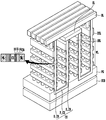
도 1a 내지 도 1c는 본 발명의 일 실시예에 따른 반도체 장치의 제조 방법을 설명하기 위한 공정 단면도이다.
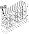
도 2a 내지 도 2d는 본 발명의 일 실시예에 따른 반도체 장치의 스트링 구조를 설명하기 위한 사시도이다.
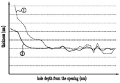
도 3은 본 발명의 일 실시예에 따른 제1 및 제2 터널절연막들의 스텝 커버리지 특성을 나타내는 그래프이다.
도 4는 본 발명의 일 실시예에 따른 반도체 장치의 소거 특성을 나타내는 그래프이다.
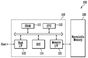
도 5는 본 발명의 일 실시예에 따른 메모리 시스템의 구성을 나타낸 구성도이다.
도 6은 본 발명의 일 실시예에 따른 컴퓨팅 시스템의 구성을 나타내는 구성도이다.1A to 1C are cross-sectional views illustrating a method of manufacturing a semiconductor device according to an embodiment of the present invention.
2A to 2D are perspective views illustrating a string structure of a semiconductor device according to an embodiment of the present invention.
3 is a graph illustrating step coverage characteristics of first and second tunnel insulating layers according to an embodiment of the present invention.
4 is a graph showing erase characteristics of a semiconductor device according to an embodiment of the present invention.
5 is a block diagram showing a configuration of a memory system according to an embodiment of the present invention.
6 is a configuration diagram illustrating a configuration of a computing system according to an embodiment of the present invention.
이하에서는, 본 발명의 가장 바람직한 실시예가 설명된다. 도면에 있어서, 두께와 간격은 설명의 편의를 위하여 표현된 것이며, 실제 물리적 두께에 비해 과장되어 도시될 수 있다. 본 발명을 설명함에 있어서, 본 발명의 요지와 무관한 공지의 구성은 생략될 수 있다. 각 도면의 구성요소들에 참조 번호를 부가함에 있어서, 동일한 구성 요소들에 한해서는 비록 다른 도면상에 표시되더라도 가능한 한 동일한 번호를 가지도록 하고 있음에 유의하여야 한다.
Hereinafter, the most preferred embodiment of the present invention will be described. In the drawings, the thickness and the spacing are expressed for convenience of explanation, and can be exaggerated relative to the actual physical thickness. In describing the present invention, known configurations irrespective of the gist of the present invention may be omitted. It should be noted that, in the case of adding the reference numerals to the constituent elements of the drawings, the same constituent elements have the same number as much as possible even if they are displayed on different drawings.
도 1a 내지 도 1c는 본 발명의 일 실시예에 따른 반도체 장치의 제조 방법을 설명하기 위한 공정 단면도이다. 단, 설명의 편의를 위해, 메모리 셀들이 형성된 영역만을 도시하고, 그 외의 영역은 생략하였다.1A to 1C are cross-sectional views illustrating a method of manufacturing a semiconductor device according to an embodiment of the present invention. However, for convenience of explanation, only the region where the memory cells are formed is shown, and the other regions are omitted.
도 1a에 도시된 바와 같이, 제1 물질막들(11) 및 제2 물질막들(12)을 교대로 형성한다. 여기서, 제1 물질막들(11)은 콘트롤 게이트들을 형성하기 위한 희생막이고, 제2 물질막(12)은 층간절연막을 형성하기 위한 것이다. As shown in FIG. 1A,
참고로, 메모리 셀들의 콘트롤 게이트들과 선택 트랜치스터의 선택 게이트 모두 제1 물질막들(11)을 이용하여 형성할 수 있다. 예를 들어, 제1 물질막들(11) 중 최상부 적어도 하나의 제1 물질막(11)은 선택 게이트를 형성하기 위한 것이고, 나머지 제1 물질막들(11)은 콘트롤 게이트를 형성하기 위한 것일 수 있다. 여기서, 선택 라인용 제1 물질막(11)과 워드라인용 제1 물질막(11)은 동일한 두께로 형성되거나, 상이한 두께로 형성될 수 있다. 예를 들어, 선택 라인용 제1 물질막(11)은 워드라인용 제1 물질막(11)에 비해 두꺼운 두께로 형성될 수 있다.For reference, both the control gates of the memory cells and the selection gates of the selection trenches can be formed using the
또한, 제1 물질막들(11)과 제2 물질막들(12)은 식각 선택비가 큰 물질로 형성된다. 일 예로, 제1 물질막들(11)은 산화막, 질화막, 도프드 폴리실리콘막 등의 희생막으로 형성되고, 제2 물질막들(12)은 산화막 등의 절연막으로 형성될 수 있다. 다른 예로, 제1 물질막들(11)은 산화막, 질화막, 도프드 폴리실리콘막 등의 제1 희생막으로 형성되고, 제2 물질막들(12)은 산화막, 질화막, 언도프드 폴리실리콘막, 언도프드 비정질 실리콘막 등의 제2 희생막으로 형성될 수 있다. Also, the
본 실시예에서는 제1 물질막들(11)은 희생막으로 형성되고, 제2 물질막들은 절연막으로 형성된 경우에 대해 설명하도록 한다. In this embodiment, the case where the first
이어서, 제1 및 제2 물질막들(11, 12)을 관통하는 홀을 형성한다. 이어서, 홀 내에 데이터 저장막(14)을 형성한다. 여기서, 데이터 저장막(14)은 전하를 저장하는 폴리실리콘막 등의 전하저장막, 전하를 트랩하는 질화막 등의 전하트랩막, 나노 닷 및 상변화 물질막 중 적어도 하나를 포함할 수 있다. Subsequently, holes are formed through the first and
참고로, 데이터 저장막(14)을 형성하기 전에, 홀 내에 버퍼막(13)을 형성할 수 있다. 여기서, 버퍼막(13)은 후속 리세스 영역 형성 공정에서, 데이터 저장막(14)이 손상되는 것을 방지하기 위한 것으로, 일종의 보호막으로 사용된다. 예를 들어, 버퍼막(13)은 산화막을 포함한다. For reference, before forming the
이어서, 데이터 저장막(14) 상에 제1 터널절연막(15)을 형성한 후, 제1 터널절연막(15) 상에 제2 터널절연막(16)을 형성한다. 여기서, 제1 및 제2 터널절연막들(15, 16)은 산화막을 포함한다. 또한, 제1 및 제2 터널절연막들(15, 16)은 상이한 방식을 이용하여 형성된다. Then, a first
일 예로, 제1 터널절연막(15)은 열산화(thermal oxidation) 방식을 이용하여 형성할 수 있다. 이러한 경우, 데이터 저장막(14)을 일부 두께 산화시켜 제1 터널절연막(15)을 형성하며, 데이터 저장막(14)은 산화될 두께를 고려하여 충분히 두껍게 형성된다. 열산화 방식으로 형성된 제1 터널절연막(15)은 막질 및 계면 특성이 우수하고, 두께가 균일하다는 장점이 있다. For example, the first
다른 예로, 제1 터널절연막(15)은 ALD(Atomic Layer Deposition) 등의 증착 방식을 이용하여 형성할 수 있다. ALD 방식으로 형성된 제1 터널절연막(15)은 두께가 균일하다는 장점이 있다. As another example, the first
제2 터널절연막(16)은 LP-CVD(Low Pressure-Chemical Vapor Deposition) 등의 증착 방식을 이용하여 형성할 수 있다. LP-CVD 방식으로 형성된 제2 터널절연막(16)은 막 내의 결함(defect), 고정 전하(fixed charge) 분포 등의 특성상, 소거 특성이 우수한 장점이 있다.The second tunnel
이로써, 제1 및 제2 터널절연막들(15, 16)이 형성되며, 이들은 각 메모리 셀들의 터널절연막으로서 사용된다. 참고로, 본 실시예에서는 이중막으로 터널절연막을 형성하는 경우에 대해 설명하였으나, 삼중막 이상의 멀티막으로 터널절연막을 형성하는 것도 가능하다. 멀티막으로 터널절연막을 형성하는 경우, 앞서 설명한 방식들을 조합하여 터널절연막을 형성할 수 있다. Thereby, first and second
이어서, 제2 터널절연막(16) 상에 채널막(17)을 형성한다. 여기서, 채널막(17)은 필라 형태 또는 튜브 형태로 형성될 수 있다. 튜브 형태로 채널막(17)을 형성하는 경우, 채널막(17)의 오픈된 중심 영역에 절연막(18)을 형성한다. Then, a
도 1b에 도시된 바와 같이, 제1 및 제2 물질막들(11, 12)을 관통하는 슬릿(SL)을 형성한 후, 슬릿(SL)에 노출된 제1 물질막들(11)을 제거하여 리세스 영역들(RC)을 형성한다. The slits SL passing through the first and
이어서, 홀 내에 버퍼막(13)이 형성된 경우에는, 리세스 영역들(RC)에 노출된 버퍼막(13)을 식각하여 버퍼막 패턴들(13A)을 형성한다. Subsequently, when the
도 1c에 도시된 바와 같이, 리세스 영역들(RC) 내에 전하차단막(19)을 형성한다. 예를 들어, 리세스 영역들(RC)이 형성된 결과물의 전면을 따라 전하차단막(19)을 형성한다. 전하차단막(19)은 고유전상수(high k) 물질막 및 산화막 중 적어도 하나를 포함한다. As shown in Fig. 1C, the
이어서, 전하차단막(19)이 형성된 리세스 영역들(RC) 내에 도전막들(20)을 형성한다. 이어서, 슬릿(SL) 내에 절연막(21)을 형성한다. 이때, 절연막(21)의 증착 조건을 조절하여, 슬릿(SL) 내에 에어 갭을 형성할 수 있다.Then, the
이로써, 채널막(17)을 따라 적층된 메모리 셀들(MC)이 형성된다. 여기서, 각 메모리 셀들(MC)은 채널막(17), 채널막(17)을 감싸는 도전막(20), 채널막(17)과 도전막(20) 사이에 개재된 제1 터널절연막(15), 제1 터널절연막(15)을 감싸는 데이터 저장막(14), 제1 터널절연막(15)과 채널막(17) 사이에 개재된 제2 터널절연막(16) 및 데이터 저장막(14)과 도전막들(20) 사이에 개재된 전하차단막(19)을 포함한다. Thereby, the memory cells MC stacked along the
여기서, 도전막(20)은 콘트롤 게이트(CG)로 사용되고, 절연막(12)은 층간절연막(IIL)으로 사용될 수 있다. 전하차단막(19)은 각각의 도전막들(20)의 상부면 및 하부면을 감싸는 형태로 형성될 수 있다. 또한, 데이터 저장막(14)과 절연막들(12) 사이에는 버퍼막 패턴들(13A)이 개재될 수 있다. Here, the
전술한 바와 같은 실시예에 따르면, 상이한 방식을 이용하여 제1 및 제2 터널절연막들(15, 16)을 형성하며, 이들은 각 메모리 셀들(MC)의 터널절연막으로서 사용된다. 여기서, 터널절연막은 전하의 터널링을 위한 에너지 장벽막으로 사용된다. 따라서, 채널막(17)과 접하는 영역에는 소거 특성이 우수한 제2 터널절연막(16)을 형성하고, 데이터 저장막(14)과 접하는 영역에는 두께 균일도가 높은 제1 터널절연막(15)을 형성함으로써, 터널절연막의 두께 균일도를 증가시킴과 동시에 반도체 장치의 소거 특성을 향상시킬 수 있다.
According to the embodiment described above, the first and second
한편, 제1 및 제2 물질막들(11, 12)의 종류에 따라 앞서 설명한 제조 공정은 일부 변경될 수 있다.The manufacturing process described above may be partially changed depending on the types of the first and
예를 들어, 제1 물질막들(11)은 제1 희생막으로 형성되고 제2 물질막들(12)은 제2 희생막으로 형성될 수 있다. 이러한 경우, 제1 및 제2 물질막들(11, 12)을 형성한 후, 도전막(20)을 형성하는 공정까지 동일하게 실시한다. 이어서, 슬릿(SL) 내에 노출된 전하차단막(19)을 식각한 후, 제2 물질막들(12)을 제거하여 리세스 영역들을 형성한다. 이어서, 리세스 영역들 내에 노출된 버퍼막 패턴들(13A) 및 데이터 저장막(14)을 식각한다. 이어서, 리세스 영역들 내에 절연막들을 형성한 후, 슬릿(SL) 내에 절연막(21)을 형성한다. For example, the
이와 같은 공정에 따르면, 적층된 메모리 셀들(MC)의 데이터 저장막(14)을 상호 분리시킴으로써, 반도체 장치의 데이터 리텐션 특성을 향상시킬 수 있다.
According to such a process, the data retention characteristics of the semiconductor device can be improved by separating the
도 2a 내지 도 2d는 본 발명의 일 실시예에 따른 반도체 장치의 스트링 구조를 설명하기 위한 사시도이다. 단, 설명의 편의를 위해 절연막은 생략하고 도시하였다. 2A to 2D are perspective views illustrating a string structure of a semiconductor device according to an embodiment of the present invention. However, the insulating film is omitted for convenience of explanation.
도 2a는 스트링들이 U형태로 배열된 경우를 나타낸다.Fig. 2A shows a case where strings are arranged in U-shape.
도 2a에 도시된 바와 같이, 반도체 장치는 기판(SUB) 상에 적층된 파이프 게이트(PG), 워드라인들(WL), 적어도 하나의 드레인 선택 라인들(DSL) 및 적어도 하나의 소스 선택 라인들(SSL)을 포함한다. 2A, the semiconductor device includes a substrate PUB, a word line WL, at least one drain select line DSL, and at least one source select line SD, which are stacked on a substrate SUB. (SSL).
반도체 장치는 U형태의 채널막들(CH)을 더 포함한다. 여기서, 채널막들(CH)은 파이프 게이트(PG) 내에 형성된 파이프 채널막(P_CH) 및 파이프 채널막(P_CH)과 연결된 소스 및 드레인 사이드 채널막들(S_CH, D_CH)을 포함한다. The semiconductor device further includes U-shaped channel films (CH). Here, the channel films CH include source and drain side channel films S_CH and D_CH connected to the pipe channel film P_CH formed in the pipe gate PG and the pipe channel film P_CH.
여기서, 소스 사이드 채널막들(S_CH)은 워드라인들(WL) 및 소스 선택 라인들(SSL)을 관통하고, 드레인 사이드 채널막들(D_CH)은 워드라인들(WL) 및 드레인 선택 라인들(DSL)을 관통한다. 또한, 소스 사이드 채널막들(S_CH)은 소스 라인(SL)과 연결되고, 드레인 사이드 채널막들(D_CH)은 비트라인들(BL)과 연결된다.Here, the source side channel films S_CH extend through the word lines WL and the source selection lines SSL and the drain side channel films D_CH extend through the word lines WL and drain selection lines DSL). The source side channel films S_CH are connected to the source line SL and the drain side channel films D_CH are connected to the bit lines BL.
또한, 반도체 장치는 채널막들(CH)과 워드라인들(WL) 사이에 개재된 제1 및 제2 터널절연막들(15, 16), 데이터 저장막(14) 및 전하차단막(19)을 더 포함한다.The semiconductor device further includes first and second
이와 같은 구조에 따르면, 직렬로 연결된 적어도 하나의 드레인 선택 트랜지스터, 메모리 셀들, 적어도 하나의 소스 선택 트랜지스터가 하나의 스트링을 구성하며, 스트링들은 U형태로 배열된다.
According to such a structure, at least one drain selection transistor, memory cells, and at least one source selection transistor connected in series form one string, and the strings are arranged in U-shape.
도 2b는 스트링이 수직 형태로 배열된 경우를 나타낸다.FIG. 2B shows a case where the strings are arranged in a vertical form.
도 2b에 도시된 바와 같이, 반도체 장치는 소스 영역(S)이 형성된 기판(SUB) 상에 차례로 적층된 적어도 하나의 하부 선택 라인(LSL), 워드라인들(WL), 및 적어도 하나의 상부 선택 라인(USL)을 포함한다. 여기서, 워드라인들(WL)은 플레이트 형태를 갖고, 상부 및 하부 선택 라인들(USL,LSL) 중 적어도 하나는 라인 형태를 갖는다.2B, the semiconductor device includes at least one lower select line LSL, word lines WL, and at least one upper select line LSL, which are sequentially stacked on a substrate SUB on which a source region S is formed. Line USL. Here, the word lines WL have a plate shape, and at least one of the upper and lower selection lines USL and LSL has a line shape.
반도체 장치는 기판(SUB)으로부터 돌출되어 하부 선택 라인(LSL), 워드라인들(WL) 및 상부 선택 라인들(USL)을 관통하는 채널막들(CH)을 더 포함한다. 여기서, 채널막들(CH)의 상단은 비트라인들(BL)과 연결되고, 채널막들(CH)의 하단은 소스 영역(S)과 연결된다. The semiconductor device further includes channel films CH protruding from the substrate SUB and passing through the lower select line LSL, the word lines WL and the upper select lines USL. The upper end of the channel films CH is connected to the bit lines BL and the lower end of the channel films CH is connected to the source region S. [
또한, 반도체 장치는 채널막들(CH)과 워드라인들(WL) 사이에 개재된 제1 및 제2 터널절연막들(15, 16), 데이터 저장막(14) 및 전하차단막(19)을 더 포함한다.The semiconductor device further includes first and second
이와 같은 구조에 따르면, 직렬로 연결된 적어도 하나의 하부 선택 트랜지스터, 메모리 셀들, 적어도 하나의 상부 선택 트랜지스터가 하나의 스트링을 구성하며, 스트링들은 수직 형태로 배열된다.
According to this structure, the at least one lower selection transistor connected in series, the memory cells, the at least one upper selection transistor constitute one string, and the strings are arranged in a vertical form.
도 2c는 스트링이 수직 형태로 배열된 경우를 나타낸다. FIG. 2C shows a case where the strings are arranged in a vertical form.
도 2c에 도시된 바와 같이, 반도체 장치는 차례로 적층된 소스막(S1~S3), 적어도 하나의 하부 선택 라인(LSL), 워드라인들(WL) 및 적어도 하나의 상부 선택 라인들(USL)을 포함한다. As shown in FIG. 2C, the semiconductor device includes a source film S1 to S3, at least one lower selection line LSL, word lines WL, and at least one upper selection lines USL .
여기서, 소스막(S1~S3)은 기판(SUB) 상에 형성된 제1 소스막, 제1 소스막(S1) 내에 형성된 제3 소스막(S3), 제3 소스막(S3)을 감싸면서 제1 소스막(S1)과 제3 소스막(S3) 사이에 개재된 제2 소스막(S2)을 포함한다. 또한, 제3 소스막(S3)은 제2 소스막(S2)을 관통하여 제1 소스막(S1)과 연결된다. 여기서, 제1 및 제2 소스막들(S1, S2)은 폴리실리콘막을 포함하고, 제3 소스막(S3)은 텅스텐(W) 등의 금속막을 포함한다. The source films S1 to S3 include a first source film formed on the substrate SUB, a third source film S3 formed in the first source film S1 and a third source film S3, And a second source film S2 sandwiched between the first source film S1 and the third source film S3. Also, the third source film S3 is connected to the first source film S1 through the second source film S2. Here, the first and second source films S1 and S2 include a polysilicon film, and the third source film S3 includes a metal film such as tungsten (W).
반도체 장치는 제2 소스막(S2)의 상부면으로부터 돌출되어 하부 선택 라인(LSL), 워드라인들(WL) 및 상부 선택 라인들(USL)을 관통하는 채널막들(CH)을 더 포함한다. 여기서, 채널막들(CH)은 제2 소스막(S2)과 일체로 연결되어 형성될 수 있다. 또한, 채널막들(CH)의 상단은 비트라인들(BL)과 연결된다.The semiconductor device further includes channel films CH protruding from the upper surface of the second source film S2 and penetrating the lower select line LSL, the word lines WL and the upper select lines USL . Here, the channel films CH may be formed integrally with the second source film S2. In addition, the upper end of the channel films CH is connected to the bit lines BL.
또한, 반도체 장치는 채널막들(CH)과 워드라인들(WL) 사이에 개재된 제1 및 제2 터널절연막들(15, 16), 데이터 저장막(14) 및 전하차단막(19)을 더 포함한다. 여기서, 제1 터널절연막(15), 제2 터널절연막(16) 및 데이터 저장막(14)은 채널막들(CH) 및 제2 소스막(S2)의 외측면(outer surfac)을 감싸는 형태로 형성된다. The semiconductor device further includes first and second
이와 같은 구조에 따르면, 직렬로 연결된 적어도 하나의 하부 선택 트랜지스터, 메모리 셀들, 적어도 하나의 상부 선택 트랜지스터가 하나의 스트링을 구성하며, 스트링들은 수직 형태로 배열된다.
According to this structure, the at least one lower selection transistor connected in series, the memory cells, the at least one upper selection transistor constitute one string, and the strings are arranged in a vertical form.
도 2d는 스트링이 수직 형태로 배열된 경우를 나타낸다. Fig. 2D shows a case where the strings are arranged in a vertical form.
도 2d에 도시된 바와 같이, 반도체 장치는 차례로 적층된 층간절연막(IIL), 적어도 하나의 하부 선택 라인(LSL), 워드라인들(WL) 및 적어도 하나의 상부 선택 라인(USL)을 포함하고, 층간절연막(IIL) 내에 형성된 제1 소스막(S1) 및 제1 소스막(S1) 내에 형성된 제2 소스막(S2)을 포함한다. 2D, the semiconductor device includes an interlayer insulating film IIL, at least one lower select line LSL, word lines WL, and at least one upper select line USL, A first source film S1 formed in the interlayer insulating film IIL and a second source film S2 formed in the first source film S1.
반도체 장치는 제1 소스막(S1)으로부터 돌출되어 하부 선택 라인(LSL), 워드라인들(WL) 및 상부 선택 라인들(USL)을 관통하는 채널막들(CH)을 더 포함한다. 여기서, 채널막들(CH)은 제1 소스막(S1)과 일체로 연결되어 형성될 수 있다. 또한, 채널막들(CH)의 상단은 비트라인들(BL)과 연결된다.The semiconductor device further includes channel films CH protruding from the first source film S1 and penetrating the lower select line LSL, the word lines WL and the upper select lines USL. Here, the channel films CH may be formed integrally with the first source film S1. In addition, the upper end of the channel films CH is connected to the bit lines BL.
또한, 반도체 장치는 채널막들(CH)과 워드라인들(WL) 사이에 개재된 제1 및 제2 터널절연막들(15, 16), 데이터 저장막(14) 및 전하차단막(19)을 더 포함한다. 여기서, 제1 터널절연막(15), 제2 터널절연막(16) 및 데이터 저장막(14)은 채널막들(CH) 및 제1 소스막(S1)의 외측면(outer surfac)을 감싸는 형태로 형성된다. The semiconductor device further includes first and second
본 도면에서는 제1 소스막(S1)이 제2 소스막(S2)의 하부면을 완전히 감싸는 구조를 도시하였으나, 제2 소스막(S2)의 하부면이 일부 돌출되어 제1 소스막(S1)을 관통하는 것도 가능하다. Although the first source film S1 completely covers the lower surface of the second source film S2 in the figure, the lower surface of the second source film S2 is partially protruded to form the first source film S1. .
이와 같은 구조에 따르면, 직렬로 연결된 적어도 하나의 하부 선택 트랜지스터, 메모리 셀들, 적어도 하나의 상부 선택 트랜지스터가 하나의 스트링을 구성하며, 스트링들은 수직 형태로 배열된다. According to this structure, the at least one lower selection transistor connected in series, the memory cells, the at least one upper selection transistor constitute one string, and the strings are arranged in a vertical form.
참고로, 도 2a 내지 도 2d를 참조하여 설명한 반도체 장치들은 앞서 설명한 제조 방법을 응용하여 제조할 수 있으며, 구체적인 제조 방법에 대한 설명은 생략하도록 한다.
For reference, the semiconductor devices described with reference to FIGS. 2A to 2D can be manufactured by applying the manufacturing method described above, and a detailed description of the manufacturing method will be omitted.
도 3은 본 발명의 일 실시예에 따른 반도체 장치에 포함된 터널절연막의 두께 균일도를 나타내는 그래프이다. 여기서, X축은 홀의 개구부로부터 깊이를 나타내고, Y축은 터널절연막의 두께를 나타낸다. 3 is a graph showing the thickness uniformity of a tunnel insulating film included in a semiconductor device according to an embodiment of the present invention. Here, the X axis represents the depth from the opening of the hole, and the Y axis represents the thickness of the tunnel insulating film.
본 그래프는 LP-CVD 방식으로 단일 터널절연막을 형성한 경우(①)와 열산화 증착 방식 및 LP-CVD 방식으로 이중 터널절연막을 형성한 경우(②)의 두께 균일도를 비교하여 도시하고 있다. This graph shows the uniformity of thickness in the case of forming a single tunnel insulating film by the LP-CVD method (1) and the case of forming the double tunnel insulating film by the thermal oxidation deposition method and the LP-CVD method (2).
그래프를 살펴보면, 단일 터널절연막을 형성한 경우(①), 홀의 개구부와 심부의 터널절연막 두께 차이가 크다. 이를 통해, 단일 터널절연막은 두께 균일도가 낮음을 알 수 있다. 반면에, 이중 터널절연막을 형성한 경우(②), 홀의 개구부와 심부의 터널절연막 두께 차이가 작다. 이를 통해, 이중 터널절연막은 두께 균일도가 높음을 알 수 있다. In the graph, when a single tunnel insulating film is formed (1), there is a large difference in the thickness of the tunnel insulating film between the hole and the deep portion of the hole. As a result, it can be seen that the thickness uniformity of the single tunnel insulating film is low. On the other hand, when the double tunnel insulating film is formed (②), the difference in the thickness of the tunnel insulating film between the hole and the deep portion of the hole is small. As a result, it can be seen that the double tunnel insulating film has a high thickness uniformity.
즉, 본 발명의 일 실시예에 따르면, 상이한 방식으로 이중 터널절연막을 형성함으로써, 터널절연막의 두께 균일도를 향상시킬 수 있음을 확인하였다.
That is, according to an embodiment of the present invention, it has been confirmed that the uniformity of the thickness of the tunnel insulating film can be improved by forming the double tunnel insulating film in a different manner.
도 4는 본 발명의 일 실시예에 따른 반도체 장치의 소거 특성을 나타내는 그래프이다. 여기서, X축은 소거 전압을 나타내고, Y축은 메모리 셀의 문턱 전압(Vt)을 나타낸다. 4 is a graph showing erase characteristics of a semiconductor device according to an embodiment of the present invention. Here, the X-axis represents the erase voltage and the Y-axis represents the threshold voltage (Vt) of the memory cell.
본 그래프는 LP-CVD 방식으로 단일 터널절연막을 형성한 경우(①)와 열산화 증착 방식 및 LP-CVD 방식으로 이중 터널절연막을 형성한 경우(②)의 두께 균일도를 비교하여 도시하고 있다. This graph shows the uniformity of thickness in the case of forming a single tunnel insulating film by the LP-CVD method (1) and the case of forming the double tunnel insulating film by the thermal oxidation deposition method and the LP-CVD method (2).
그래프에서, "P"는 프로그램된 상태를 나타내고, "E1~E4"는 소거 상태를 나타낸다. 또한, "E1~E4"는 소거 전압의 레벨의 차이에 따른 메모리 셀의 문턱 전압의 변화를 나타내기 위한 것으로 숫자가 증가할수록 소거 전압의 레벨이 증가된다.In the graph, "P" indicates the programmed state, and "E1 through E4" indicates the erased state. In addition, "E1 to E4" denotes a change in the threshold voltage of the memory cell in accordance with the difference in level of the erase voltage, and the level of the erase voltage increases as the number increases.
그래프를 살펴보면, 소거 전압을 레벨을 증가시킬수록 소거 동작시 메모리 셀의 문턱 전압 변동 값이 증가된다. 또한, 동일한 소거 전압을 사용한 경우, 단일 터널절연막을 형성한 경우(①)에 비해 이중 터널절연막을 형성한 경우(②)가 문턱 전압(Vt)의 변동 값이 크다. 이를 통해, 이중 터널절연막을 형성함으로써 메모리 셀의 문턱 전압 변동 폭을 증가시킬 수 있음을 알 수 있다. In the graph, as the erase voltage is increased, the threshold voltage variation value of the memory cell is increased in the erase operation. Further, when the same erasing voltage is used, the variation value of the threshold voltage (Vt) is larger when the double tunnel insulating film is formed (2) than when the single tunnel insulating film is formed (1). As a result, it can be seen that the width of the threshold voltage fluctuation of the memory cell can be increased by forming the double tunnel insulating film.
즉, 본 발명의 일 실시예에 따르면, 상이한 방식을 이용하여 이중 터널절연막을 형성함으로써, 반도체 장치의 소거 특성을 향상시킬 수 있다.
That is, according to one embodiment of the present invention, the erasing characteristics of the semiconductor device can be improved by forming the double tunnel insulating film using a different method.
도 5는 본 발명의 일 실시예에 따른 메모리 시스템의 구성을 나타낸 구성도이다.5 is a block diagram showing a configuration of a memory system according to an embodiment of the present invention.
도 5에 도시된 바와 같이, 본 발명의 일 실시예에 따른 메모리 시스템(100)은 비휘발성 메모리 소자(120)와 메모리 컨트롤러(110)를 포함한다. As shown in FIG. 5, a
비휘발성 메모리 소자(120)는 앞서 설명된 구조를 갖는다. 또한, 비휘발성 메모리 소자(120)는 복수의 플래시 메모리 칩들로 구성된 멀티-칩 패키지일 수 있다.The
메모리 컨트롤러(110)는 비휘발성 메모리 소자(120)를 제어하도록 구성되며, SRAM(111), CPU(112), 호스트 인터페이스(113), ECC(114), 메모리 인터페이스(115)를 포함할 수 있다. SRAM(111)은 CPU(112)의 동작 메모리로 사용되고, CPU(112)는 메모리 컨트롤러(110)의 데이터 교환을 위한 제반 제어 동작을 수행하고, 호스트 인터페이스(113)는 메모리 시스템(100)과 접속되는 호스트의 데이터 교환 프로토콜을 구비한다. 또한, ECC(114)는 비휘발성 메모리 소자(120)로부터 리드된 데이터에 포함된 에러를 검출 및 정정하고, 메모리 인터페이스(115)는 비휘발성 메모리 소자(120)와의 인터페이싱을 수행한다. 이 밖에도 메모리 컨트롤러(110)는 호스트와의 인터페이싱을 위한 코드 데이터를 저장하는 ROM 등을 더 포함할 수 있다.The
이와 같은 구성을 갖는 메모리 시스템(100)은 비휘발성 메모리 소자(120)와 컨트롤러(110)가 결합된 메모리 카드 또는 SSD(Solid State Disk)일 수 있다. 예를 들어, 메모리 시스템(100)이 SSD인 경우, 메모리 컨트롤러(110)는 USB, MMC, PCI-E, SATA, PATA, SCSI, ESDI, IDE 등과 같은 다양한 인터페이스 프로토콜들 중 하나를 통해 외부(예를 들어, 호스트)와 통신할 수 있다.
The
도 6은 본 발명의 일 실시예에 따른 컴퓨팅 시스템의 구성을 나타내는 구성도이다.6 is a configuration diagram illustrating a configuration of a computing system according to an embodiment of the present invention.
도 6에 도시된 바와 같이, 본 발명의 일 실시예에 따른 컴퓨팅 시스템(200)은 시스템 버스(260)에 전기적으로 연결된 CPU(220), RAM(230), 유저 인터페이스(240), 모뎀(250), 메모리 시스템(210)을 포함할 수 있다. 또한, 컴퓨팅 시스템(200)이 모바일 장치인 경우, 컴퓨팅 시스템(200)에 동작 전압을 공급하기 위한 베터리가 더 포함될 수 있으며, 응용 칩셋, 카메라 이미지 프로세서(CIS), 모바일 디렘 등이 더 포함될 수 있다.6, a
메모리 시스템(210)은 앞서 도 5를 참조하여 설명한 바와 같이, 비휘발성 메모리(212), 메모리 컨트롤러(211)로 구성될 수 있다.
The
본 발명의 기술 사상은 상기 바람직한 실시예들에 따라 구체적으로 기록되었으나, 상기한 실시예는 그 설명을 위한 것이며 그 제한을 위한 것이 아님을 주의하여야 한다. 또한, 본 발명의 기술 분야의 통상의 전문가라면 본 발명의 기술 사상의 범위내에서 다양한 실시예가 가능함을 이해할 수 있을 것이다.
It is to be noted that the technical spirit of the present invention has been specifically described in accordance with the above-described preferred embodiments, but it is to be understood that the above-described embodiments are intended to be illustrative and not restrictive. In addition, it will be understood by those of ordinary skill in the art that various embodiments are possible within the scope of the technical idea of the present invention.
11: 제1 물질막 12: 제2 물질막
13: 버퍼막 14: 데이터 저장막
15: 제1 터널절연막 16: 제2 터널절연막
17: 채널막 18: 절연막
19: 전하차단막 20: 도전막
21: 절연막11: First material film 12: Second material film
13: buffer film 14: data storage film
15: first tunnel insulating film 16: second tunnel insulating film
17: channel film 18: insulating film
19: charge blocking film 20: conductive film
21: Insulating film
Claims (15)
상기 도전막들 및 층간절연막들을 관통하는 채널막;
상기 채널막과 상기 도전막들 사이에 개재되며, 열산화 방식으로 형성된 제1 터널절연막;
상기 제1 터널절연막을 감싸는 데이터 저장막; 및
상기 제1 터널절연막과 상기 채널막 사이에 개재되며, 증착 방식으로 형성된 제2 터널절연막
을 포함하는 반도체 장치.
Alternately stacked conductive films and interlayer insulating films;
A channel film penetrating the conductive films and the interlayer insulating films;
A first tunnel insulating film interposed between the channel film and the conductive films, the first tunnel insulating film being formed by a thermal oxidation method;
A data storage layer surrounding the first tunnel insulating layer; And
A second tunnel insulating film interposed between the first tunnel insulating film and the channel film,
≪ / RTI >
상기 증착 방식은 LP-CVD(Low Pressure-Chemical Vapor Deposition) 방식인
반도체 장치.
The method according to claim 1,
The deposition method is an LP-CVD (Low Pressure-Chemical Vapor Deposition)
A semiconductor device.
상기 제1 터널절연막은 상기 데이터 저장막을 일부 두께 산화시켜 형성된
반도체 장치.
The method according to claim 1,
The first tunnel insulating film is formed by partially oxidizing the data storage film
A semiconductor device.
상기 도전막들 및 층간절연막들을 관통하는 채널막;
상기 채널막과 상기 도전막들 사이에 개재되며, 제1 증착 방식으로 형성된 제1 터널절연막;
상기 제1 터널절연막을 감싸는 데이터 저장막; 및
상기 제1 터널절연막과 상기 채널막 사이에 개재되며, 제2 증착 방식으로 형성된 제2 터널절연막
을 포함하는 반도체 장치.
Alternately stacked conductive films and interlayer insulating films;
A channel film penetrating the conductive films and the interlayer insulating films;
A first tunnel insulating film interposed between the channel film and the conductive films, the first tunnel insulating film being formed by a first deposition method;
A data storage layer surrounding the first tunnel insulating layer; And
A second tunnel insulating film interposed between the first tunnel insulating film and the channel film,
≪ / RTI >
상기 제1 증착 방식은 ALD(Atomic Layer Deposition) 방식이고, 상기 제2 증착 방식은 LP-CVD (Low Pressure-Chemical Vapor Deposition) 방식인
반도체 장치.
5. The method of claim 4,
The first deposition method is an ALD (Atomic Layer Deposition) method, and the second deposition method is an LP-CVD (Low Pressure-Chemical Vapor Deposition)
A semiconductor device.
상기 데이터 저장막과 상기 층간절연막들 사이에 개재된 버퍼막 패턴들
을 더 포함하는 반도체 장치.
The method according to claim 1 or 4,
The buffer film patterns interposed between the data storage film and the interlayer insulating films
Further comprising:
상기 데이터 저장막과 상기 도전막들 사이에 개재된 전하차단막
을 더 포함하는 반도체 장치.
The method according to claim 1 or 4,
The data storage film and the charge blocking film interposed between the conductive films
Further comprising:
상기 전하차단막은 상기 도전막들의 상부면 및 하부면을 감싸는
반도체 장치.
8. The method of claim 7,
The charge blocking film is formed on the upper surface and the lower surface of the conductive films
A semiconductor device.
상기 제1 및 제2 물질막들을 관통하는 홀을 형성하는 단계;
상기 홀 내에 데이터 저장막을 형성하는 단계;
상기 데이터 저장막 상에, 제1 방식으로 제1 터널절연막을 형성하는 단계;
상기 제1 터널절연막 상에, 제2 방식으로 제2 터널절연막을 형성하는 단계; 및
상기 제2 터널절연막 상에 채널막을 형성하는 단계
를 포함하는 반도체 장치의 제조 방법.
Alternately forming first material layers and second material layers;
Forming a hole through the first and second material layers;
Forming a data storage layer in the hole;
Forming a first tunnel insulating film on the data storage film in a first manner;
Forming a second tunnel insulating film on the first tunnel insulating film in a second manner; And
Forming a channel film on the second tunnel insulating film
Wherein the semiconductor device is a semiconductor device.
상기 제1 방식은 열산화 방식이고, 상기 제2 방식은 LP-CVD(Low Pressure-Chemical Vapor Deposition) 방식인
반도체 장치의 제조 방법.
10. The method of claim 9,
The first method is a thermal oxidation method, and the second method is a LP-CVD (Low Pressure-Chemical Vapor Deposition)
A method of manufacturing a semiconductor device.
상기 제1 터널절연막은 상기 데이터 저장막을 일부 두께 산화시켜 형성된
반도체 장치의 제조 방법.
11. The method of claim 10,
The first tunnel insulating film is formed by partially oxidizing the data storage film
A method of manufacturing a semiconductor device.
상기 제1 방식은 ALD(Atomic Layer Deposition) 방식이고, 상기 제2 방식은 LP-CVD(Low Pressure-Chemical Vapor Deposition) 방식인
반도체 장치의 제조 방법.
10. The method of claim 9,
The first scheme is an ALD (Atomic Layer Deposition) scheme, and the second scheme is an LP-CVD (Low Pressure Chemical Vapor Deposition) scheme
A method of manufacturing a semiconductor device.
상기 데이터 저장막을 형성하기 전에, 상기 홀 내에 버퍼막을 형성하는 단계
를 더 포함하는 반도체 장치의 제조 방법.
10. The method of claim 9,
Forming a buffer film in the hole before forming the data storage film;
Further comprising the steps of:
상기 제1 및 제2 물질막들을 관통하는 슬릿을 형성하는 단계;
상기 슬릿 내에 노출된 상기 제1 물질막들을 제거하여 리세스 영역들을 형성하는 단계;
상기 리세스 영역들 내에 노출된 상기 버퍼막을 식각하여 버퍼막 패턴들을 형성하는 단계; 및
상기 리세스 영역들 내에 도전막들을 형성하는 단계
를 더 포함하는 반도체 장치의 제조 방법.
14. The method of claim 13,
Forming a slit through the first and second material layers;
Removing the first material layers exposed in the slit to form recess regions;
Etching the buffer film exposed in the recessed regions to form buffer film patterns; And
Forming conductive films in the recess regions
Further comprising the steps of:
상기 도전막들을 형성하기 전에, 상기 리세스 영역들 내에 전하차단막을 형성하는 단계
를 더 포함하는 반도체 장치의 제조 방법.
15. The method of claim 14,
Forming a charge blocking film in the recessed regions before forming the conductive films,
Further comprising the steps of:
Priority Applications (1)
| Application Number | Priority Date | Filing Date | Title |
|---|---|---|---|
| KR1020120147514A KR20140078297A (en) | 2012-12-17 | 2012-12-17 | Semiconductor device and method for manufacturing the same |
Applications Claiming Priority (1)
| Application Number | Priority Date | Filing Date | Title |
|---|---|---|---|
| KR1020120147514A KR20140078297A (en) | 2012-12-17 | 2012-12-17 | Semiconductor device and method for manufacturing the same |
Publications (1)
| Publication Number | Publication Date |
|---|---|
| KR20140078297A true KR20140078297A (en) | 2014-06-25 |
Family
ID=51129942
Family Applications (1)
| Application Number | Title | Priority Date | Filing Date |
|---|---|---|---|
| KR1020120147514A Withdrawn KR20140078297A (en) | 2012-12-17 | 2012-12-17 | Semiconductor device and method for manufacturing the same |
Country Status (1)
| Country | Link |
|---|---|
| KR (1) | KR20140078297A (en) |
Cited By (2)
| Publication number | Priority date | Publication date | Assignee | Title |
|---|---|---|---|---|
| KR20170136364A (en) * | 2016-06-01 | 2017-12-11 | 에스케이하이닉스 주식회사 | Method of manufacturing semiconductor device |
| CN109300900A (en) * | 2018-10-16 | 2019-02-01 | 长江存储科技有限责任公司 | Three-dimensional memory and method of forming three-dimensional memory |
-
2012
- 2012-12-17 KR KR1020120147514A patent/KR20140078297A/en not_active Withdrawn
Cited By (3)
| Publication number | Priority date | Publication date | Assignee | Title |
|---|---|---|---|---|
| KR20170136364A (en) * | 2016-06-01 | 2017-12-11 | 에스케이하이닉스 주식회사 | Method of manufacturing semiconductor device |
| CN109300900A (en) * | 2018-10-16 | 2019-02-01 | 长江存储科技有限责任公司 | Three-dimensional memory and method of forming three-dimensional memory |
| CN109300900B (en) * | 2018-10-16 | 2020-07-07 | 长江存储科技有限责任公司 | Three-dimensional memory and method for forming three-dimensional memory |
Similar Documents
| Publication | Publication Date | Title |
|---|---|---|
| US10424597B2 (en) | Semiconductor device and manufacturing method thereof | |
| KR102401867B1 (en) | Memory Arrays, and Methods of Forming the Memory Arrays | |
| KR102421606B1 (en) | Memory Arrays and Methods of Forming Memory Arrays | |
| KR101979458B1 (en) | Semiconductor device and method for manufacturing the same | |
| KR102101841B1 (en) | Vertical type non-volatile memory device | |
| US8748966B2 (en) | Three dimensional non-volatile memory device and method of manufacturing the same | |
| CN102760738B (en) | 3D non-volatile memory device and its production method | |
| CN103515392B (en) | Semiconductor devices and its manufacture method | |
| US8872254B2 (en) | Semiconductor device and method of manufacturing the same | |
| US9041090B2 (en) | Methods for forming a string of memory cells and apparatuses having a vertical string of memory cells including metal | |
| JP2013165266A (en) | Semiconductor device and method of manufacturing the same | |
| US8698231B2 (en) | Semiconductor device and method of manufacturing the same | |
| KR20190019672A (en) | Semiconductor device and method of manufacturing the same | |
| KR20150001999A (en) | Semiconductor memory device and method of manufacturing the same | |
| KR20130123165A (en) | Semiconductor device and method of manufacturing the same | |
| KR20130089076A (en) | Semiconductor device and method of manufacturing the same | |
| US9287289B2 (en) | Semiconductor device and method of manufacturing the same | |
| KR20130070158A (en) | 3-dimensional non-volatile memoy device, memory system and method of manufacturing the same | |
| US20130043521A1 (en) | 3-dimensional non-volatile memory device and method of manufacturing the same | |
| US20150129947A1 (en) | Nonvolatile semiconductor storage device | |
| CN106663682A (en) | Method for manufacturing semiconductor device | |
| KR20150004653A (en) | Semiconductor memory device and method of manufacturing the same | |
| KR20140020145A (en) | Method of manufacturing the non-volatile memory device | |
| KR20140078297A (en) | Semiconductor device and method for manufacturing the same | |
| KR20200141841A (en) | Semiconductor device and method of manufacturing the same |
Legal Events
| Date | Code | Title | Description |
|---|---|---|---|
| PA0109 | Patent application |
Patent event code: PA01091R01D Comment text: Patent Application Patent event date: 20121217 |
|
| PG1501 | Laying open of application | ||
| PC1203 | Withdrawal of no request for examination | ||
| WITN | Application deemed withdrawn, e.g. because no request for examination was filed or no examination fee was paid |