KR20210073587A - Anthracene derivatives and organic electronic devices using same - Google Patents
Anthracene derivatives and organic electronic devices using same Download PDFInfo
- Publication number
- KR20210073587A KR20210073587A KR1020217016056A KR20217016056A KR20210073587A KR 20210073587 A KR20210073587 A KR 20210073587A KR 1020217016056 A KR1020217016056 A KR 1020217016056A KR 20217016056 A KR20217016056 A KR 20217016056A KR 20210073587 A KR20210073587 A KR 20210073587A
- Authority
- KR
- South Korea
- Prior art keywords
- group
- formula
- substituted
- organic
- compound
- Prior art date
- Legal status (The legal status is an assumption and is not a legal conclusion. Google has not performed a legal analysis and makes no representation as to the accuracy of the status listed.)
- Granted
Links
Images

Classifications
-
- C—CHEMISTRY; METALLURGY
- C07—ORGANIC CHEMISTRY
- C07D—HETEROCYCLIC COMPOUNDS
- C07D307/00—Heterocyclic compounds containing five-membered rings having one oxygen atom as the only ring hetero atom
- C07D307/77—Heterocyclic compounds containing five-membered rings having one oxygen atom as the only ring hetero atom ortho- or peri-condensed with carbocyclic rings or ring systems
- C07D307/91—Dibenzofurans; Hydrogenated dibenzofurans
-
- C—CHEMISTRY; METALLURGY
- C09—DYES; PAINTS; POLISHES; NATURAL RESINS; ADHESIVES; COMPOSITIONS NOT OTHERWISE PROVIDED FOR; APPLICATIONS OF MATERIALS NOT OTHERWISE PROVIDED FOR
- C09K—MATERIALS FOR MISCELLANEOUS APPLICATIONS, NOT PROVIDED FOR ELSEWHERE
- C09K11/00—Luminescent materials, e.g. electroluminescent or chemiluminescent
- C09K11/06—Luminescent materials, e.g. electroluminescent or chemiluminescent containing organic luminescent materials
-
- H01L51/0052—
-
- H01L51/0073—
-
- H01L51/5012—
-
- H—ELECTRICITY
- H10—SEMICONDUCTOR DEVICES; ELECTRIC SOLID-STATE DEVICES NOT OTHERWISE PROVIDED FOR
- H10K—ORGANIC ELECTRIC SOLID-STATE DEVICES
- H10K50/00—Organic light-emitting devices
- H10K50/10—OLEDs or polymer light-emitting diodes [PLED]
- H10K50/11—OLEDs or polymer light-emitting diodes [PLED] characterised by the electroluminescent [EL] layers
-
- H—ELECTRICITY
- H10—SEMICONDUCTOR DEVICES; ELECTRIC SOLID-STATE DEVICES NOT OTHERWISE PROVIDED FOR
- H10K—ORGANIC ELECTRIC SOLID-STATE DEVICES
- H10K85/00—Organic materials used in the body or electrodes of devices covered by this subclass
- H10K85/60—Organic compounds having low molecular weight
- H10K85/615—Polycyclic condensed aromatic hydrocarbons, e.g. anthracene
-
- H—ELECTRICITY
- H10—SEMICONDUCTOR DEVICES; ELECTRIC SOLID-STATE DEVICES NOT OTHERWISE PROVIDED FOR
- H10K—ORGANIC ELECTRIC SOLID-STATE DEVICES
- H10K85/00—Organic materials used in the body or electrodes of devices covered by this subclass
- H10K85/60—Organic compounds having low molecular weight
- H10K85/649—Aromatic compounds comprising a hetero atom
- H10K85/657—Polycyclic condensed heteroaromatic hydrocarbons
- H10K85/6574—Polycyclic condensed heteroaromatic hydrocarbons comprising only oxygen in the heteroaromatic polycondensed ring system, e.g. cumarine dyes
-
- C—CHEMISTRY; METALLURGY
- C09—DYES; PAINTS; POLISHES; NATURAL RESINS; ADHESIVES; COMPOSITIONS NOT OTHERWISE PROVIDED FOR; APPLICATIONS OF MATERIALS NOT OTHERWISE PROVIDED FOR
- C09K—MATERIALS FOR MISCELLANEOUS APPLICATIONS, NOT PROVIDED FOR ELSEWHERE
- C09K2211/00—Chemical nature of organic luminescent or tenebrescent compounds
- C09K2211/10—Non-macromolecular compounds
- C09K2211/1003—Carbocyclic compounds
- C09K2211/1011—Condensed systems
-
- C—CHEMISTRY; METALLURGY
- C09—DYES; PAINTS; POLISHES; NATURAL RESINS; ADHESIVES; COMPOSITIONS NOT OTHERWISE PROVIDED FOR; APPLICATIONS OF MATERIALS NOT OTHERWISE PROVIDED FOR
- C09K—MATERIALS FOR MISCELLANEOUS APPLICATIONS, NOT PROVIDED FOR ELSEWHERE
- C09K2211/00—Chemical nature of organic luminescent or tenebrescent compounds
- C09K2211/10—Non-macromolecular compounds
- C09K2211/1018—Heterocyclic compounds
- C09K2211/1025—Heterocyclic compounds characterised by ligands
- C09K2211/1088—Heterocyclic compounds characterised by ligands containing oxygen as the only heteroatom
-
- Y—GENERAL TAGGING OF NEW TECHNOLOGICAL DEVELOPMENTS; GENERAL TAGGING OF CROSS-SECTIONAL TECHNOLOGIES SPANNING OVER SEVERAL SECTIONS OF THE IPC; TECHNICAL SUBJECTS COVERED BY FORMER USPC CROSS-REFERENCE ART COLLECTIONS [XRACs] AND DIGESTS
- Y02—TECHNOLOGIES OR APPLICATIONS FOR MITIGATION OR ADAPTATION AGAINST CLIMATE CHANGE
- Y02E—REDUCTION OF GREENHOUSE GAS [GHG] EMISSIONS, RELATED TO ENERGY GENERATION, TRANSMISSION OR DISTRIBUTION
- Y02E10/00—Energy generation through renewable energy sources
- Y02E10/50—Photovoltaic [PV] energy
- Y02E10/549—Organic PV cells
Landscapes
- Chemical & Material Sciences (AREA)
- Organic Chemistry (AREA)
- Engineering & Computer Science (AREA)
- Materials Engineering (AREA)
- Physics & Mathematics (AREA)
- Spectroscopy & Molecular Physics (AREA)
- Optics & Photonics (AREA)
- Electroluminescent Light Sources (AREA)
- Furan Compounds (AREA)
Abstract
본 발명은, 유기 전자 디바이스, 특히 유기 EL 디바이스를 위한 재료, 특히 발광 재료로서 유용한 신규 화합물 및 그를 사용한 유기 전자 디바이스, 특히 유기 EL 디바이스를 제공하는 것을 목적으로 한다.An object of the present invention is to provide a novel compound useful as a material for an organic electronic device, in particular an organic EL device, in particular a light emitting material, and an organic electronic device using the same, in particular an organic EL device.
Description
본 명세서는 2019년 02월 20일 일본특허청에 제출된 일본 특허 출원 제2019-028321호의 출원일의 이익을 주장하며, 그 내용 전부는 본 명세서에 포함된다.This specification claims the benefit of the filing date of Japanese Patent Application No. 2019-028321 filed with the Japan Patent Office on February 20, 2019, the entire contents of which are incorporated herein by reference.
본 발명은, 안트라센 유도체, 및 그를 이용한 유기 전자 디바이스, 예를 들면 유기 태양 전지, 유기 감광체(OPC), 유기 발광 디바이스, 보다 상세하게는 유기 일렉트로 루미네선스(EL) 디바이스, 유기 트랜지스터, 특히 유기 발광 디바이스, 그 중에서도 유기 EL 디바이스에 관한 것이다. 본 발명의 안트라센 유도체는, 특히 유기 EL 디바이스를 위한 발광 재료로서 유용하다.The present invention relates to anthracene derivatives and organic electronic devices using them, such as organic solar cells, organic photoconductors (OPCs), organic light emitting devices, more particularly organic electroluminescence (EL) devices, organic transistors, especially organic It relates to a light emitting device, especially an organic EL device. The anthracene derivative of the present invention is particularly useful as a light emitting material for an organic EL device.
유기 전자 디바이스는, 정공 및/또는 전자를 사용한, 디바이스를 구성하는 전극과 유기물층 간에서의 전하의 수송을 필요로 하는 소자이다. 유기 전자 디바이스는, 동작 원리에 따라 이하와 같이 크게 2개의 종류로 나눌 수 있다. 제1의 종류의 디바이스는, 외부의 광원으로부터 디바이스에 입사한 광자에 의해 유기물층에 있어서 여기자가 형성되어, 이 여기자가 전자와 정공으로 분리되고, 이 전자와 정공이 각각 별개의 전극에 수송되어 발생하는 기전력을 이용하는 형태의 전자 디바이스이다. 제2의 종류의 디바이스는, 2개 이상의 별개의 전극에 전압을 인가하거나 또는 디바이스에 전류를 흘려, 각각의 전극에 접하는 유기물 반도체층에 정공 및/또는 전자를 주입하고, 주입된 전자와 정공에 의해 동작하는 형태의 전자 디바이스이다. 제1의 종류의 디바이스에는, 예를 들면 유기 태양 전지 및 유기 감광체(OPC)가 포함된다. 제2의 종류의 디바이스에는, 예를 들면 유기 발광 디바이스, 보다 상세하게는 유기 일렉트로 루미네선스(EL) 디바이스, 유기 트랜지스터가 포함된다.An organic electronic device is an element that requires transport of electric charge between an electrode constituting the device and an organic substance layer using holes and/or electrons. Organic electronic devices can be roughly divided into two types as follows according to the operation principle. In the first type of device, excitons are formed in the organic material layer by photons incident on the device from an external light source, the excitons are separated into electrons and holes, and the electrons and holes are transported to separate electrodes, respectively. It is a type of electronic device that uses electromotive force. The second type of device applies a voltage to two or more separate electrodes or flows a current to the device to inject holes and/or electrons into the organic semiconductor layer in contact with each electrode, and inject electrons and holes into the injected electrons and holes. It is an electronic device of the type operated by A first class of devices includes, for example, organic solar cells and organic photoconductors (OPCs). The second type of device includes, for example, an organic light emitting device, more specifically an organic electroluminescence (EL) device, and an organic transistor.
유기 전자 디바이스 중에서도, 유기 EL 디바이스는, 통상적으로 애노드와 캐소드 및 이들 전극 사이에 배치된, 발광층을 포함한 유기물층을 포함하는 구조를 갖는다. 유기 EL 디바이스에서는, 애노드 및 캐소드로부터 각각 주입된 정공 및 전자가 재결합하여 발생하는 여기자의 에너지를 이용해 발광 재료로부터 발광이 발생한다. 여기서, 일반적으로 유기 EL 디바이스의 유기물층은, 그 유기 EL 디바이스의 특성, 예를 들면 발광 효율을 높이기 위해서 각각 다른 기능을 구비한 상이한 물질을 포함하여 이루어지는 복수의 층으로 이루어지는 다층 구조를 갖고, 그들 복수의 층은, 예를 들면 정공 주입층, 정공 수송층, 발광층, 전자 수송층, 및 전자 주입층 등으로 이루어진다. 그러나, 이들 층은 그 중의 몇가지 기능을 1개의 층이 담당할 수 있고, 따라서 이들 층 중 몇개는 생략해도 된다. 또한, 이들 유기물층에 더해, 전극 표면의 평탄성을 높이기 위한 평탄화층, 발광층에 정공, 전자, 및/또는 여기자를 가두기 위한, 정공 저지층, 전자 저지층, 및/또는 정공 저지층을 유기 EL 디바이스의 유기층에 포함시킬 수도 있다.Among organic electronic devices, organic EL devices typically have a structure including an anode and a cathode and an organic material layer including a light emitting layer disposed between these electrodes. In an organic EL device, light emission is generated from a light emitting material using the energy of excitons generated by recombination of holes and electrons respectively injected from an anode and a cathode. Here, in general, the organic material layer of the organic EL device has a multilayer structure composed of a plurality of layers comprising different materials each having different functions in order to increase the characteristics of the organic EL device, for example, luminous efficiency, and a plurality of them. The layer of is composed of, for example, a hole injection layer, a hole transport layer, a light emitting layer, an electron transport layer, and an electron injection layer. However, these layers may perform several functions among them, and therefore some of these layers may be omitted. In addition to these organic material layers, a planarization layer for increasing the flatness of the electrode surface, a hole blocking layer for confining holes, electrons, and/or excitons in the light emitting layer, an electron blocking layer, and/or a hole blocking layer of the organic EL device It may be included in the organic layer.
이러한 구조를 갖는 유기 EL 디바이스에 있어서, 2개의 전극의 사이에 전압을 인가했을 경우, 애노드로부터는 정공이, 캐소드로부터는 전자가 유기물층에 주입되고, 주입된 정공과 전자가 결합했을 때에 발광성 분자에 있어서 그 분자의 바닥 상태 에너지보다 높은 에너지를 갖는 여기자가 형성되고, 이 여기자가 바닥 상태로 되돌아올 때에 발광이 발생한다. 이러한 유기 EL 디바이스는, 자발광형의 발광 디바이스이며, 종래의 백 라이트를 사용하는 액정 디바이스와 비교하여, 고휘도, 고효율, 낮은 구동 전압, 넓은 시야각, 높은 콘트라스트, 및 고속 응답 등의 특성을 가질 수 있는 것이 알려져 있다.In the organic EL device having such a structure, when a voltage is applied between two electrodes, holes are injected from the anode and electrons from the cathode are injected into the organic material layer, and when the injected holes and electrons are combined, the luminescent molecules In this case, excitons having an energy higher than the ground state energy of the molecule are formed, and light emission occurs when these excitons return to the ground state. Such an organic EL device is a self-luminous light emitting device, and compared with a liquid crystal device using a conventional backlight, it can have characteristics such as high luminance, high efficiency, low driving voltage, wide viewing angle, high contrast, and high-speed response. It is known that there is
유기 EL 디바이스에 있어서 사용되는 발광 재료는, 발광색에 따라, 청색, 녹색, 적색의 발광 재료와, 보다 좋은 천연색을 실현하기 위해서 필요한 황색 및 등색의 발광 재료로 분류할 수 있다. 또, 발광층을 하나의 물질만으로 형성했을 경우, 분자간 상호 작용에 의해 최대 발광 파장이 장파장으로 이동하여 색순도가 저하하거나, 발광 감쇠 효과에 의해 소자의 효율이 저하하거나 하는 문제가 발생할 수 있으므로, 발광의 높은 색순도 및 발광 효율의 향상을 위해서, 발광 재료와 호스트 또는 도펀트 재료를 포함하는 호스트/도펀트계를 발광층에 사용할 수 있다. The light emitting material used in the organic EL device can be classified into blue, green, and red light emitting materials and yellow and orange light emitting materials necessary for realizing a better natural color according to the emission color. In addition, when the light emitting layer is formed of only one material, the maximum emission wavelength is shifted to a longer wavelength due to intermolecular interaction, and there may be problems such as a decrease in color purity or a decrease in device efficiency due to the emission attenuation effect. In order to improve color purity and light emitting efficiency, a host/dopant system including a light emitting material and a host or dopant material may be used in the light emitting layer.
유기 EL 디바이스의 청색 발광 재료로서 사용할 수 있는 화합물로서, 예를 들면 페릴렌계 화합물, 피렌계 화합물, 크리센계 화합물, 안트라센계 화합물 등의 다환식 방향족 탄화수소, 스티렌 또는 비스스티릴벤젠 등의 스티렌계 탄화수소 화합물, 및 그들의 방향족 아미노기 치환체 등이 알려져 있다.As a compound which can be used as a blue light emitting material of an organic EL device, For example, polycyclic aromatic hydrocarbons, such as a perylene type compound, a pyrene type compound, a chrysene type compound, an anthracene type compound, A styrene type hydrocarbon, such as styrene or bisstyrylbenzene Compounds, and aromatic amino group substituents thereof, and the like are known.
발광 재료로서 사용할 수 있는 안트라센계 화합물로는, 예를 들면 미국 특허 제5,935,721호 명세서에, 9,10-디아릴 치환 안트라센이 기재되어 있다. 이 명세서에는, 그 아릴기가 또한 헤테로아릴기, 예를 들면 피리딜기 등으로 치환된 화합물도 기재되어 있다. 또, 국제공개 제2005/056505호에는, 안트라센 고리의 2위치에, 오르토 위치가 아릴기로 치환된 페닐기가 치환된 화합물과, 그것을 유기 EL 디바이스의 발광 재료로서 사용하는 것이 기재되어 있다. 또한, 국제공개 제2005/113531호의 [화학식 7]~[화학식 11]에는, 안트라센 고리에 직접 또는 아릴렌 혹은 헤테로아릴렌기를 개재하여 디벤조퓨란 또는 디벤조티오펜 고리가 그들의 4위치에서 결합된 화합물이 기재되어 있고, 이들을 발광 재료로서 유기 EL 디바이스에 사용하는 것도 기재되어 있다. 그러나, 이들 특허 문헌에는, 디벤조퓨란 또는 디벤조티오펜 고리가 그 1위치에서 직접 또는 아릴렌 혹은 헤테로아릴렌기를 개재하여 안트라센 고리에 결합된 화합물, 및 그것을 유기 EL 디바이스의 발광 재료로서 사용하는 것은 기재되지 않았다.As an anthracene-based compound usable as a light emitting material, for example, in the specification of US Patent No. 5,935,721, 9,10-diaryl substituted anthracene is described. This specification also describes compounds in which the aryl group is substituted with a heteroaryl group, for example, a pyridyl group or the like. Moreover, International Publication No. 2005/056505 describes a compound in which a phenyl group substituted with an aryl group at the ortho position at the 2-position of the anthracene ring is substituted, and the use of the compound as a light emitting material for an organic EL device. In addition, in [Formula 7] to [Formula 11] of International Publication No. 2005/113531, dibenzofuran or dibenzothiophene ring is bonded at their 4th position directly or through an arylene or heteroarylene group to the anthracene ring Compounds have been described, and their use as luminescent materials in organic EL devices is also described. However, in these patent documents, a compound in which a dibenzofuran or dibenzothiophene ring is bonded to an anthracene ring directly or via an arylene or heteroarylene group at the 1-position, and a compound in which the dibenzofuran or dibenzothiophene ring is bonded as a light emitting material of an organic EL device that was not mentioned.
상술한 바와 같이, 유기 전자 디바이스, 예를 들면 유기 EL 디바이스를 위한 재료, 예를 들면 발광 재료로서 다양한 화합물이 개발되어 왔으나, 더욱 뛰어난 특성을 갖는 화합물 또는 지금까지 알려지지 않은 신규 화학 구조를 갖는 화합물의 개발이 여전히 요구되고 있다. 본 발명은, 유기 전자 디바이스, 특히 유기 EL 디바이스를 위한 재료, 특히 발광 재료로서 유용한 신규 화합물 및 그를 이용한 유기 전자 디바이스, 특히 유기 EL 디바이스를 제공하고자 하는 것이다.As described above, various compounds have been developed as materials for organic electronic devices, for example, organic EL devices, for example, light emitting materials, but compounds having superior properties or compounds having hitherto unknown novel chemical structures have been developed. Development is still required. An object of the present invention is to provide a novel compound useful as a material for an organic electronic device, in particular an organic EL device, in particular a light emitting material, and an organic electronic device using the same, in particular an organic EL device.
상기 과제를 해결하기 위해서, 본 발명에서는 이하에 설명하는 화합물을, 유기 전자 디바이스의 재료, 특히 유기 EL 디바이스의 발광 재료로서 사용한다.In order to solve the said subject, in this invention, the compound demonstrated below is used as a material of an organic electronic device, especially as a light emitting material of an organic electroluminescent device.
본 발명의 화합물은, 하기 화학식 1:The compound of the present invention has the following formula 1:
[화학식 1][Formula 1]

[화학식 1 중, R1~R10은 각각 독립적으로, 수소 원자, 중수소 원자, 불소 원자, CN기, 치환 또는 비치환된 탄소수 1~8의 알킬기, 치환 또는 비치환된 고리 구성 원자수 6~30의 아릴기, 및 치환 또는 비치환된 고리 구성 원자수 5~30의 헤테로아릴기로 이루어지는 군으로부터 선택되고;단, R1~R4 및 R5~R8 중 적어도 1개가 하기 화학식 2:[In Formula 1, R1 to R10 are each independently a hydrogen atom, a deuterium atom, a fluorine atom, a CN group, a substituted or unsubstituted alkyl group having 1 to 8 carbon atoms, a substituted or unsubstituted ring atom number of 6 to 30 It is selected from the group consisting of an aryl group and a substituted or unsubstituted heteroaryl group having 5 to 30 ring atoms; provided that at least one of R1 to R4 and R5 to R8 is represented by Formula 2:
[화학식 2][Formula 2]

(화학식 2 중, *는 화학식 1의 안트라센 고리와의 결합 부위를 나타내고;A는 단결합, 치환 또는 비치환된 고리 구성 원자수 6~30의 아릴렌기, 또는 치환 또는 비치환된 고리 구성 원자수 5~30의 헤테로아릴렌기를 나타내고;X는 산소 원자 또는 황 원자이며;R11~R17은 각각 독립적으로, 수소 원자, 중수소 원자, 불소 원자, CN기, 치환 또는 비치환된 탄소수 1~8의 알킬기, 치환 또는 비치환된 고리 구성 원자수 6~30의 아릴기, 및 치환 또는 비치환된 고리 구성 원자수 5~30의 헤테로아릴기로 이루어지는 군으로부터 선택된다. )로 표시된다.](In
로 표시된다.is displayed as
또한 상기 화학식 1의 화합물은, 하기 화학식 3:In addition, the compound of Formula 1 is the following Formula 3:
[화학식 3][Formula 3]

(화학식 3 중, A, X, R1~R17은 위에서 정의한 바와 같다. )(In
으로 표시되는 화합물인 것이 바람직하다.It is preferable that it is a compound represented by
또한, 상기 화학식 1의 화합물은, 특히 하기 화학식 4:In addition, the compound of the formula (1) is, in particular, the following formula 4:
[화학식 4][Formula 4]

(화학식 4 중, X 및 R1~R17은 위에서 정의한 바와 같다)(In Formula 4, X and R1 to R17 are as defined above)
로 표시되는 화합물인 것이 바람직하다.It is preferable that it is a compound represented by
상기 화학식 1, 3, 및 4에 있어서, R9 및 R10은 동일하거나 또는 상이하고, 각각 치환 또는 비치환된 고리 구성 원자수 6~30의 아릴기인 것이 바람직하다.In
상기 화학식 1, 3, 및 4에 있어서, R9 및/또는 R10이 치환 아릴기인 경우, 그 치환기가 치환 또는 비치환된 고리 구성 탄소 원자수 6~30의 아릴기 및 치환 또는 비치환된 고리 구성 원자수 5~30의 헤테로아릴기로 이루어지는 군으로부터 선택되는 것이 바람직하다.In
상기 화학식 1의 화합물은, 하기 화학식 5:The compound of Formula 1 has the following Formula 5:
[화학식 5][Formula 5]

(화학식 5 중 R1, R3, R4, R5~8, 및 R11~R17, 그리고 X는 화학식 1에 대해 정의한 바와 같고;R21 및 R22는 각각 독립적으로, 중수소 원자, 탄소수 1~8의 알킬기, 치환 또는 비치환된 고리 구성 탄소 원자수 6~30의 아릴기, 및 치환 또는 비치환된 고리 구성 탄소 원자수 5~30의 헤테로아릴기를 나타내고, m 및 n은 각각 독립적으로 0~5 중 어느 한 정수를 나타낸다. )(In
로 표시되는 화합물인 것이 특히 바람직하다.It is especially preferable that it is a compound represented by
상기 화학식 5로 표시되는 화합물 중에서도, 특히, 하기 화학식 6:Among the compounds represented by the above formula (5), in particular, the following formula (6):
[화학식 6][Formula 6]

(화학식 6 중 X는 화학식 1에 대해 정의한 바와 같고;R21 및 R22는 각각 독립적으로, 중수소 원자, 탄소수 1~8의 알킬기, 치환 또는 비치환된 고리 구성 탄소 원자수 6~30의 아릴기, 및 치환 또는 비치환된 고리 구성 탄소 원자수 5~30의 헤테로아릴기를 나타내고, m 및 n은 각각 독립적으로 0~5 중 어느 한 정수를 나타낸다. )(X in Formula 6 is as defined for Formula 1; R21 and R22 are each independently a deuterium atom, an alkyl group having 1 to 8 carbon atoms, a substituted or unsubstituted aryl group having 6 to 30 carbon atoms in the ring, and represents a substituted or unsubstituted heteroaryl group having 5 to 30 ring carbon atoms, and m and n each independently represent any integer from 0 to 5.)
으로 표시되는 화합물이 바람직하다.A compound represented by
본 발명은, 상술한 화합물로 이루어지는, 유기 전자 디바이스용 재료도 제공한다.The present invention also provides a material for an organic electronic device comprising the compound described above.
상기 유기 전자 디바이스는, 유기 일렉트로 루미네선스 디바이스(유기 EL 디바이스)인 것이 바람직하다.It is preferable that the said organic electronic device is an organic electroluminescent device (organic electroluminescent device).
상기 유기 전자 디바이스용 재료는, 유기 EL 디바이스를 위한 발광 재료인 것이 특히 바람직하다.It is particularly preferable that the material for an organic electronic device is a light emitting material for an organic EL device.
본 발명은 또한, 상술한 어느 한 화합물을 포함하는, 특히 발광 재료로서 포함하는, 유기 EL 디바이스도 제공한다.The present invention also provides an organic EL device comprising any one of the compounds described above, particularly as a light emitting material.
본 출원의 일 실시상태에 따른 화합물을 사용하는 유기 전자 디바이스는 수명이 긴 장점이 있다.The organic electronic device using the compound according to an exemplary embodiment of the present application has an advantage of a long lifespan.
도 1은, 본 발명의 유기 EL 디바이스의 전형적인 구조를 나타낸 도면이다.
[부호의 설명]
1…기판
2…애노드
3…정공 주입층
4…정공 수송층
5…발광층
6…전자 수송층
7…캐소드1 is a diagram showing a typical structure of an organic EL device of the present invention.
[Explanation of code]
One… Board
2… anode
3… hole injection layer
4… hole transport layer
5… light emitting layer
6… electron transport layer
7… cathode
발명의 실시를 위한 최선의 형태Best mode for carrying out the invention
본 발명에 대해 이하에서 더욱 상세하게 설명한다.The present invention will be described in more detail below.
본 명세서에 있어서 '알킬기'에는, 직쇄상 알킬기, 분기상 알킬기, 및 환상 알킬기가 포함된다. 탄소수 1~8의 직쇄상 또는 분기상 알킬기의 예로는, 메틸, 에틸, n-프로필, 이소프로필, 시클로프로필, n-부틸, 이소부틸, tert-부틸, 펜틸, 헥실, 옥틸, 및 2-에틸헥실기 등을 들 수 있으나, 이들에 한정되지 않는다. 환상 알킬기의 예로는, 시클로프로필, 시클로부틸, 시클로펜틸, 시클로헥실, 및 이들 환상 알킬 부분 구조를 포함하는 알킬기, 예를 들면 메틸시클로프로필 및 메틸시클로헥실기 등을 들 수 있으나, 이들에 한정되지 않는다.In the present specification, the term "alkyl group" includes a linear alkyl group, a branched alkyl group, and a cyclic alkyl group. Examples of the linear or branched alkyl group having 1 to 8 carbon atoms include methyl, ethyl, n-propyl, isopropyl, cyclopropyl, n-butyl, isobutyl, tert-butyl, pentyl, hexyl, octyl, and 2-ethyl A hexyl group etc. are mentioned, However, It is not limited to these. Examples of the cyclic alkyl group include, but are not limited to, cyclopropyl, cyclobutyl, cyclopentyl, cyclohexyl, and an alkyl group containing these cyclic alkyl moieties, for example, methylcyclopropyl and methylcyclohexyl groups. does not
본 명세서에 있어서 '아릴기'는 방향족 탄화수소기를 말하며, 예를 들면 페닐, 비페닐, 터페닐, 플루오레닐, 스피로비플루오레닐, 나프틸, 안트라세닐, 페난트릴, 아세나프틸레닐, 플루오란테닐, 피레닐, 크리세닐, 트리페닐레닐, 및 페릴레닐기를 들 수 있으나, 이들에 한정되지 않는다. 본 명세서에 있어서 플루오레닐기도 광의의 아릴기 또는 치환 아릴기에 포함한다. 본 명세서에 있어서 '아릴렌기'는 상기 '아릴기'로부터 추가로 수소 원자 1개가 제거된 2가의 기를 말한다.In the present specification, the 'aryl group' refers to an aromatic hydrocarbon group, for example, phenyl, biphenyl, terphenyl, fluorenyl, spirobifluorenyl, naphthyl, anthracenyl, phenanthryl, acenaphthylenyl, fluorine lanthenyl, pyrenyl, chrysenyl, triphenylenyl, and perylenyl groups, but are not limited thereto. In the present specification, the fluorenyl group includes an aryl group or a substituted aryl group in a broad sense. In the present specification, the 'arylene group' refers to a divalent group in which one hydrogen atom has been further removed from the 'aryl group'.
본 명세서에 있어서 '헤테로아릴기'는 헤테로 원자를 고리 구성 원자로서 1개 이상 포함하는 방향족 복소환기를 말하며, 예를 들면 인데닐기, 벤조인데닐기, 피롤릴기, 인돌릴기, 카르바졸릴기, 퓨라닐기, 벤조퓨라닐기, 디벤조퓨라닐기(특히, 디벤조퓨란-1-일기, 디벤조퓨란-2-일기, 디벤조퓨란-3-일기, 및 디벤조티오펜-4-일기), 티오페닐기, 벤조티오페닐기, 디벤조티오페닐기(특히, 디벤조티오펜-1-일기, 디벤조티오펜-2-일기, 디벤조티오펜-3-일기, 및 디벤조티오펜-4-일기), 셀레노페닐기, 벤조셀레노페닐기, 디벤조셀레노페닐기(특히, 디벤조셀레노펜-1-일, 디벤조셀레노펜-2-일, 디벤조셀레노펜-3-일기, 및 디벤조셀레노펜-4-일기), 이미다졸릴기, 벤조이미다졸릴기, 트리아졸릴기, 옥사졸릴기, 옥사디아졸릴기, 티아졸릴기, 티아디아졸릴기, 피리딜기, 피리미딜기, 트리아지닐기, 퀴롤리닐기, 및 퀴녹살리닐기를 들 수 있으나, 이들에 한정되지 않는다. 본 명세서에 있어서 '헤테로아릴렌기'는 상기 '헤테로아릴기'로부터 추가로 수소 원자 1개가 제거된 2가의 기를 말한다.As used herein, the term 'heteroaryl group' refers to an aromatic heterocyclic group containing at least one hetero atom as a ring constituent atom, for example, an indenyl group, a benzoindenyl group, a pyrrolyl group, an indolyl group, a carbazolyl group, and a fura group. Nyl group, benzofuranyl group, dibenzofuranyl group (especially dibenzofuran-1-yl group, dibenzofuran-2-yl group, dibenzofuran-3-yl group, and dibenzothiophen-4-yl group), thiophenyl group , a benzothiophenyl group, a dibenzothiophenyl group (especially a dibenzothiophen-1-yl group, a dibenzothiophen-2-yl group, a dibenzothiophen-3-yl group, and a dibenzothiophen-4-yl group); selenophenyl group, benzoselenophenyl group, dibenzoselenophenyl group (especially dibenzoselenophen-1-yl, dibenzoselenophen-2-yl, dibenzoselenophen-3-yl group, and dibenzoselenophene- 4-yl group), imidazolyl group, benzoimidazolyl group, triazolyl group, oxazolyl group, oxadiazolyl group, thiazolyl group, thiadiazolyl group, pyridyl group, pyrimidyl group, triazinyl group, qui a rollinyl group, and a quinoxalinyl group, but is not limited thereto. In the present specification, the 'heteroarylene group' refers to a divalent group in which one additional hydrogen atom is removed from the 'heteroaryl group'.
본 발명의 화합물에 있어서, 상술한 알킬, 아릴, 헤테로아릴, 아릴렌, 및 헤테로아릴렌기는 각각 독립적으로 비치환이거나 또는 치환기를 갖고 있을 수 있다. 이들 치환기의 종류는 특별히 한정되지 않지만, 독립적으로, 중수소 원자, 할로겐 원자(예를 들면, 불소, 염소, 또는 브롬 원자), 시아노기, 니트로기, 탄소수 1~6의 직쇄 또는 분기상의 알킬기, 탄소수 3~6의 시클로알킬기, 탄소수 1~6의 알콕시기, 고리 탄소 원자수 6~30의 아릴 또는 고리 원자수 5~30의 헤테로아릴기, 고리 탄소 원자수 6~30의 아릴 또는 고리 원자수 5~30의 헤테로아릴옥시기, 고리 탄소 원자수 6~30의 아릴 또는 고리 원자수 5~30의 헤테로아릴기를 치환기로서 갖는 모노 또는 디 치환 아미노기, 고리 탄소 원자수 6~30의 아릴 또는 고리 원자수 5~30의 헤테로아릴기를 치환기로서 갖는 트리아릴실릴 또는 트리헤테로아릴실릴기로 이루어지는 군으로부터 선택되는 기인 것이 바람직하다. 치환기의 수는, 치환기가 존재하는 경우에는, 1부터 치환 가능한 최대수까지의 임의의 수일 수 있다.In the compound of the present invention, the aforementioned alkyl, aryl, heteroaryl, arylene, and heteroarylene groups may each independently be unsubstituted or may have a substituent. Although the type of these substituents is not particularly limited, independently, a deuterium atom, a halogen atom (eg, fluorine, chlorine, or bromine atom), a cyano group, a nitro group, a linear or branched alkyl group having 1 to 6 carbon atoms, a carbon number A cycloalkyl group having 3 to 6 carbon atoms, an alkoxy group having 1 to 6 carbon atoms, an aryl group having 6 to 30 ring carbon atoms or a heteroaryl group having 5 to 30 ring atoms, an aryl group having 6 to 30 ring carbon atoms or 5 ring atoms A mono- or disubstituted amino group having as a substituent a heteroaryloxy group of ~30, an aryl group of 6 to 30 ring atoms, or a heteroaryl group of 5 to 30 ring atoms, an aryl of 6 to 30 ring carbon atoms or ring atoms It is preferable that it is a group selected from the group which consists of a triarylsilyl or triheteroarylsilyl group which has a 5-30 heteroaryl group as a substituent. The number of substituents can be any number from 1 to the maximum number that can be substituted, when substituents are present.
특히 바람직한 치환기는, 각각 독립적으로, 중수소 원자, 고리 탄소 원자수 6~30의 아릴기, 고리 탄소 원자수 5~30의 헤테로아릴기, 모노아릴아미노기 또는 디아릴아미노기(아릴기는 고리 탄소 원자수 6~30의 아릴기이다), 및 트리아릴실릴기(아릴기는 고리 탄소 원자수 6~30의 아릴기이다)로 이루어지는 군으로부터 선택된다.Particularly preferable substituents are each independently a deuterium atom, an aryl group having 6 to 30 ring carbon atoms, a heteroaryl group having 5 to 30 ring carbon atoms, a monoarylamino group or a diarylamino group (the aryl group having 6 ring carbon atoms) -30 is an aryl group), and a triarylsilyl group (the aryl group is an aryl group having 6 to 30 ring carbon atoms).
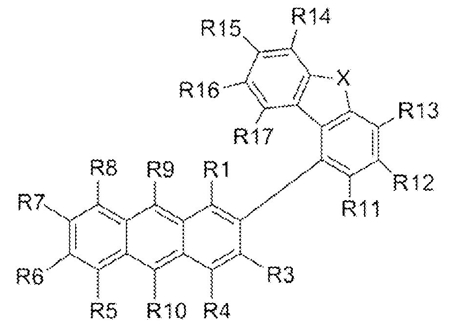
본 발명의 화합물은, 하기 화학식 1:The compound of the present invention has the following formula 1:
[화학식 1][Formula 1]

로 표시된다.is displayed as
화학식 1 중, R1~R10은 각각 독립적으로, 수소 원자, 중수소 원자, 불소 원자, CN기, 치환 또는 비치환된 탄소수 1~8의 알킬기, 치환 또는 비치환된 고리 구성 원자수 6~30의 아릴기, 및 치환 또는 비치환된 고리 구성 원자수 5~30의 헤테로아릴기로 이루어지는 군으로부터 선택되는 기를 나타낸다.In Formula 1, R1 to R10 are each independently a hydrogen atom, a deuterium atom, a fluorine atom, a CN group, a substituted or unsubstituted C 1 to C 8 alkyl group, or a substituted or unsubstituted aryl having 6 to 30 ring atoms. group, and a group selected from the group consisting of a substituted or unsubstituted heteroaryl group having 5 to 30 ring atoms.
단, 화학식 1에 있어서, R1~R4 및 R5~R8 중 적어도 1개가, 바람직하게는 R2, R3, R6, 및 R7 중 어느 1개 또는 2개가, 더욱 바람직하게는, R2, R3, R6, 및 R7중 1개가, 혹은 R2 및 R6, R3 및 R7, R2 및 R7, 또는 R3 및 R6이, 독립적으로, 하기 화학식 2:However, in the general formula (1), at least one of R1 to R4 and R5 to R8, preferably any one or two of R2, R3, R6, and R7, more preferably R2, R3, R6, and One of R7, or R2 and R6, R3 and R7, R2 and R7, or R3 and R6, is independently,
[화학식 2][Formula 2]

로 표시되는 기인 것을 조건으로 한다. R2, R3, R6, 및 R7 중 2개 이상이 화학식 2로 표시되는 기인 경우, 그들은 같은 기인 것이 바람직하다.It is conditional that it is a group represented by . When two or more of R2, R3, R6, and R7 are groups represented by the formula (2), they are preferably the same group.
화학식 2 중, *는 화학식 1의 안트라센 고리와의 결합 부위를 나타내고;A는 단결합, 치환 또는 비치환된 고리 구성 원자수 6~30의 아릴렌기, 또는 치환 또는 비치환된 고리 구성 원자수 5~30의 헤테로아릴렌기, 바람직하게는, 단결합 또는 비치환된 아릴렌기, 특히 바람직하게는 단결합을 나타내고;X는 산소 원자 또는 황 원자, 바람직하게는 산소 원자이며;R11~R17은 각각 독립적으로, 수소 원자, 중수소 원자, 불소 원자, CN기, 치환 또는 비치환된 탄소수 1~8의 알킬기, 치환 또는 비치환된 고리 구성 원자수 6~30의 아릴기, 및 치환 또는 비치환된 고리 구성 원자수 5~30의 헤테로아릴기로 이루어지는 군으로부터 선택된다. R11~R17은 독립적으로 수소 또는 중수소인 것이 특히 바람직하다. A가 나타내는 아릴렌기는, 독립적으로, 페닐렌, 비페닐렌, 또는 나프틸렌기인 것이 바람직하다.In
화학식 1의 정의 중, 알킬, 아릴, 헤테로아릴, 아릴렌, 헤테로아릴렌, 및 그들이 갖고 있어도 되는 치환기는 상술한 바와 같다.In the definition of formula (1), alkyl, aryl, heteroaryl, arylene, heteroarylene, and the substituents they may have are as described above.
상기 화학식 1로 표시되는 화합물은, 하기 화학식 3:The compound represented by Formula 1 is the following Formula 3:
[화학식 3][Formula 3]

으로 표시되는, 안트라센 고리의 2, 3, 6, 또는 7위치에 상기 화학식 2로 표시되는 기가 1위치 또는 9위치에서 결합된 화합물인 것이 바람직하다.It is preferable that the group represented by
화학식 3 중, A, X, R1~R17은 위의 화학식 1 및 2에 대해서 정의한 바와 같다.In
또한 상기 화학식 1의 화합물은, 하기 화학식 4:In addition, the compound of formula (1) has the following formula 4:
[화학식 4][Formula 4]

로 표시되는 화합물인 것이 바람직하다. 화학식 4의 화합물은, 상기 화학식 3에 있어서 A가 단결합인 경우이다.It is preferable that it is a compound represented by In the compound of formula (4), in the formula (3), A is a single bond.
화학식 4 중, X 및 R1~R17은 위의 화학식 1 및 2에 대해서 정의한 바와 같다.In Formula 4, X and R1 to R17 are as defined for
또한, 상기 화학식 1, 3, 및 4에 있어서, R9 및 R10은 동일하거나 또는 상이하고, 각각 치환 또는 비치환된 고리 구성 원자수 6~30의 아릴기인 것이 바람직하다. R9 및 R10이 나타내는 치환 또는 비치환 아릴기는, 페닐, 톨릴, 디메틸페닐, tert-부틸페닐, 비페닐, 터페닐, 1- 또는 2-나프틸, 및 페난트레닐로 이루어지는 군으로부터 독립적으로 선택되는 기인 것이 바람직하다.In addition, in
또, 상기 화학식 1, 3, 및 4에 있어서, R9 및/또는 R10이 치환 아릴기인 경우, 그 치환기가 치환 또는 비치환된 고리 구성 탄소 원자수 6~30의 아릴기 및 치환 또는 비치환된 고리 구성 원자수 5~30의 헤테로아릴기로 이루어지는 군으로부터 선택되는 기인 것이 바람직하다. 이들 아릴 및 헤테로아릴기가 갖고 있어도 되는 치환기는 위에서 말한 바와 같다.In addition, in
또한, 상기 화학식 1, 3, 및 4에 있어서, R9 및 R10은 동일하거나 또는 상이하고, 바람직하게는 동일하고, 각각 치환 또는 비치환된 고리 구성 원자수 6~30의 아릴기이며, 또한 R1, R3, R4, R5, R6, R7, 및 R8이 독립적으로 수소 또는 중수소 원자, 바람직하게는 수소 원자인 것이 바람직하다. 고리 구성 원자수 6~30의 아릴기가 갖고 있어도 되는 치환기는 상술한 바와 같으나, 비치환인 것이 특히 바람직하다.In addition, in
화학식 1의 화합물 중에서도 특히 바람직한 화합물은, 하기 화학식 5:Among the compounds of the general formula (1), a particularly preferred compound is a compound represented by the following general formula (5):
[화학식 5][Formula 5]

로 표시되는 화합물이다.is a compound represented by
화학식 5 중, R1, R3, R4, R5~8, 및 R11~R17, 그리고 X는 화학식 1에 대해 정의한 바와 같고 ;R21 및 R22는 각각 독립적으로, 중수소 원자, 탄소수 1~8의 알킬기, 치환 또는 비치환된 고리 구성 탄소 원자수 6~30의 아릴기, 및 치환 또는 비치환된 고리 구성 탄소 원자수 5~30의 헤테로아릴기, 특히 바람직하게는 각각 독립적으로 중수소 원자, 탄소수 1~8의 알킬기, 또는 비치환된 고리 구성 탄소 원자수 6~30의 아릴기를 나타내고, m 및 n은 각각 독립적으로 0~5 중 어느 한 정수, 바람직하게는 0 또는 1, 특히 바람직하게는 0을 나타낸다. X는 산소 원자인 것이 바람직하다.In
상기 화학식 5로 표시되는 화합물 중에서도, 특히, 하기 화학식 6:Among the compounds represented by the above formula (5), in particular, the following formula (6):
[화학식 6][Formula 6]

으로 표시되는 화합물이 바람직하다.A compound represented by
화학식 6에 있어서, X, R21, R22, m, 및 n은 상기 화학식 5에 대해 정의한 바와 같다. X는 산소 원자인 것이 바람직하다. R21 및 R22는 독립적으로, 탄소수 1~8의 알킬기, 또는 비치환된 고리 구성 탄소 원자수 6~30의 아릴기인 것이 바람직하다.In Formula 6, X, R21, R22, m, and n are as defined for
본 발명의 화합물의 구체적인 예를 이하에 나타내는데, 본 발명의 화합물은 이들에 한정되지 않는다.Specific examples of the compound of the present invention are shown below, but the compound of the present invention is not limited thereto.


(이들 식 중, X는 O 또는 S를 나타낸다. )(In these formulas, X represents O or S.)
본 발명의 화합물은, 분자 내에 안트라센 고리와, 디벤조퓨란-1-일 또는 디벤조티오펜-1-일기(또는, 디벤조퓨란-9-일 또는 디벤조티오펜-9-일기)를 갖고, 디벤조퓨란 또는 디벤조티오펜 고리가 그 1위치(또는 9위치)에서 결합되어 있는 것에 의해, 디벤조퓨란 또는 디벤조티오펜 고리가 그 4위치 등의 다른 위치에서 결합된 이성체와 비교해, 본 발명의 화합물을 발광 재료로서 사용했을 경우에, 보다 뛰어난 특성을 갖는 유기 EL 디바이스가 얻어진다고 하는 효과를 발휘할 수 있다.The compound of the present invention has an anthracene ring and a dibenzofuran-1-yl or dibenzothiophen-1-yl group (or a dibenzofuran-9-yl or dibenzothiophen-9-yl group) in the molecule, , Compared with the isomer in which the dibenzofuran or dibenzothiophene ring is bonded at the 1st position (or 9th position), the dibenzofuran or dibenzothiophene ring is bonded at other positions such as the 4th position, When the compound of this invention is used as a light emitting material, the effect that the organic electroluminescent device which has more outstanding characteristics is obtained can be exhibited.
따라서, 상술한 본 발명의 화합물은, 유기 전자 디바이스용의 재료, 특히 유기 EL 디바이스를 위한 재료, 특히 유기 EL디바이스를 위한 발광 재료, 바람직하게는 청색 발광 재료로서 사용할 수 있다.Therefore, the compound of the present invention described above can be used as a material for an organic electronic device, particularly a material for an organic EL device, particularly a light emitting material for an organic EL device, preferably a blue light emitting material.
따라서, 본 발명은, 본 발명의 화합물을 포함하는, 유기 EL 디바이스에 관한 것이기도 하다.Accordingly, the present invention also relates to an organic EL device comprising the compound of the present invention.
[유기 일렉트로 루미네선스 디바이스(유기 EL 디바이스)][Organic electroluminescence device (organic EL device)]
유기 EL 디바이스는, 일반적으로, 제1 전극과 제2 전극 및 이 사이에 배치된 1개 이상의 유기물층을 포함하고, 제1 전극 및 제2 전극 중 적어도 1개가 광투과성 전극이다. 이들 2개의 전극의 사이에 전압을 인가하여, 유기층에 애노드로부터 정공을 주입하고, 캐소드로부터 전자를 주입하면, 정공과 전자가 유기물층 중에서 재결합하고, 재결합에 의해 발생하는 여기자의 에너지를 이용하여 유기물층 중에 포함되는 발광체 즉 발광 재료가 발광한다. 유기 EL 디바이스는, 그 유기물층으로부터의 발광을, 광투과성 전극측으로부터 취출하는 구조를 갖는다. 유기 EL 디바이스의 디바이스 구조는 하나에 한정되지 않고, 다양한 디바이스 구조가 제안되어 있다. 발광 방식에 대해서도, 탑 에미션형, 보텀 에미션형, 및 양면 에미션(양면 발광)형 등이 알려져 있다. 본 발명의 유기 EL 디바이스의 유기물층은 1층으로 이루어지는 단층 구조여도 되나, 발광층을 포함하는 2층 이상의 다층 구조여도 된다. 본 발명의 유기 EL 디바이스의 유기물층이 다층 구조를 갖는 경우는, 예를 들면 정공 주입층, 정공 수송층, 발광층, 전자 수송층 등이 적층된 구조여도 된다. 또한, 전극 표면을 평탄화하기 위한 평탄화층, 정공 저지층, 전자 저지층, 및 여기자 저지층 등의 다양한 층을 설치하여, 유기 EL 디바이스의 특성을 향상시킬 수 있는 것이 알려져 있다. 상술한 본 발명의 화합물은, 모든 발광 방식 및 구조의 유기 EL 디바이스에서 사용할 수 있다. 따라서, 본 발명의 화합물을 포함하는 유기 EL 디바이스는, 그 발광의 방식 및 디바이스 구조는 특정 것에 한정되지 않는다. 또, 본 발명의 상기 화합물은, 유기 EL 디바이스를 위한 발광 재료, 특히 청색 발광 재료로서 유용하다.An organic EL device generally includes a first electrode and a second electrode and one or more organic material layers disposed therebetween, and at least one of the first electrode and the second electrode is a light-transmitting electrode. When a voltage is applied between these two electrodes to inject holes from the anode into the organic layer and electrons from the cathode, the holes and electrons recombine in the organic layer, and the energy of excitons generated by recombination is used to enter the organic layer The included light emitting body, that is, the light emitting material emits light. The organic EL device has a structure in which light emitted from the organic substance layer is extracted from the light-transmitting electrode side. The device structure of the organic EL device is not limited to one, and various device structures have been proposed. As for the light emission method, a top emission type, a bottom emission type, a double-sided emission type (double-sided light emission) type, etc. are known. The organic substance layer of the organic EL device of the present invention may have a single-layer structure consisting of one layer, or may have a multilayer structure of two or more layers including a light-emitting layer. When the organic substance layer of the organic EL device of the present invention has a multilayer structure, for example, a structure in which a hole injection layer, a hole transport layer, a light emitting layer, an electron transport layer and the like are laminated may be employed. It is also known that various layers such as a planarization layer, a hole blocking layer, an electron blocking layer, and an exciton blocking layer for planarizing an electrode surface can be provided to improve the characteristics of an organic EL device. The compound of the present invention described above can be used in an organic EL device of any light emitting method and structure. Accordingly, the organic EL device containing the compound of the present invention is not limited to a specific one in terms of its light emission mode and device structure. Moreover, the said compound of this invention is useful as a light-emitting material for organic electroluminescent devices, especially a blue light-emitting material.
유기 EL 디바이스의 전형적인 구조를 도 1에 나타낸다. 도 1에 있어서, 1은 기판, 2는 애노드, 3은 정공 주입층, 4는 정공 수송층, 5는 유기 발광층, 6은 전자 수송층, 그리고 7은 캐소드를 나타내고 있다. 통상적으로 도 1과 같은 구조의 유기 EL 디바이스를 정방향 구조의 유기 EL 디바이스라고 한다. 본 발명의 유기 EL 디바이스는, 이러한 정방향 구조일 수 있으나, 이 구조의 것에 한정되지 않고, 역방향 구조의 유기 EL 디바이스, 즉, 기판, 캐소드, 전자 수송층, 유기 발광층, 정공 수송층, 정공 주입층 및 양극이 순차적으로 적층된 구조를 갖고 있어도 된다. 또, 이들 복수의 유기층에서 몇개를 생략할 수도 있다. 또, 본 발명의 유기 EL 디바이스는, 상술한 디바이스 구조의 것에 한정되지 않고, 유기 EL 디바이스의 구조로서 공지의 어떠한 디바이스 구조를 갖고 있어도 된다.A typical structure of an organic EL device is shown in FIG. 1 . In FIG. 1 , 1 is a substrate, 2 is an anode, 3 is a hole injection layer, 4 is a hole transport layer, 5 is an organic light emitting layer, 6 is an electron transport layer, and 7 is a cathode. In general, an organic EL device having a structure as shown in FIG. 1 is referred to as an organic EL device having a forward structure. The organic EL device of the present invention may have such a forward structure, but is not limited to that of this structure, and an organic EL device of a reverse structure, that is, a substrate, a cathode, an electron transport layer, an organic light emitting layer, a hole transport layer, a hole injection layer, and an anode You may have this sequentially laminated structure. Moreover, some can also be abbreviate|omitted from these some organic layer. Moreover, the organic electroluminescent device of this invention is not limited to the thing of the device structure mentioned above, You may have any well-known device structure as a structure of an organic electroluminescent device.
본 발명에 따른 유기 EL 디바이스는, 본 발명의 화합물을 유기층에 포함하는 것을 조건으로 하는 것 외에는, 공지의 유기 EL 디바이스의 제조 방법 및 유기 EL 디바이스에 사용되는 재료를 사용하여 제조할 수 있다. 예를 들면, 본 발명에 따른 유기 EL 디바이스는, 스퍼터링이나 전자빔 증착 등의 물리 증착(PVD) 법을 이용하여, 기판 상에 금속, 합금, 또는 도전성을 갖는 금속 산화물, 및 그들의 조합을 증착하여 애노드를 형성하고, 그 위에 정공 주입층, 정공 수송층, 발광층 및 전자 수송층 등에서 선택되는 발광층을 포함한 1개 이상의 층을 포함하는 유기물층을 형성한 후, 그 위에 캐소드로서 사용할 수 있는 물질을 증착함으로써 제조할 수 있다. 이러한 방법 외에도, 상술한 것처럼 역방향 구조의 유기 EL 디바이스를 제작하기 위해서, 기판 상에 캐소드 물질부터 유기물층, 애노드 물질을 순차적으로 증착하여 유기 EL 디바이스를 만들 수도 있다. 또, 상술한 유기물층 중 몇개를 생략하는 것 및 상술한 것 이외의 유기물층을 추가할 수도 있다.The organic EL device according to the present invention can be manufactured using a known method for manufacturing an organic EL device and a material used for the organic EL device, except that the compound of the present invention is included in the organic layer. For example, the organic EL device according to the present invention uses a physical vapor deposition (PVD) method such as sputtering or electron beam vapor deposition to deposit a metal, an alloy, or a conductive metal oxide, and a combination thereof on a substrate to form an anode After forming an organic material layer comprising one or more layers including a light emitting layer selected from a hole injection layer, a hole transport layer, a light emitting layer and an electron transport layer, etc. thereon, a material that can be used as a cathode is deposited thereon. have. In addition to this method, as described above, in order to fabricate an organic EL device having a reverse structure, an organic EL device may be manufactured by sequentially depositing a cathode material, an organic material layer, and an anode material on a substrate. In addition, some of the above-mentioned organic material layers may be omitted, and organic material layers other than those described above may be added.
유기물층을 형성하는 방법으로서, 증착법 외에, 용액법, 예를 들면, 스핀 코팅, 딥 코팅, 닥터 블레이드 코팅, 스크린 인쇄, 또는 잉크젯 인쇄, 혹은 열전사법등의 방법을 사용할 수도 있다. 또한, 유기 EL 디바이스 중의 상이한 유기층에 대해서, 용액법과 증착법을 조합하여 사용할 수도 있다.As a method of forming the organic layer, in addition to the vapor deposition method, a solution method, for example, spin coating, dip coating, doctor blade coating, screen printing, inkjet printing, or a method such as thermal transfer may be used. Moreover, you can also use combining the solution method and the vapor deposition method about the different organic layers in an organic electroluminescent device.
애노드를 위한 재료로는, 통상적으로, 유기물층으로의 정공 주입이 원활해지도록 일함수가 큰 물질을 사용하는 것이 바람직하다. 본 발명에서 사용되는 애노드 재료의 구체적인 예로는, 바나듐, 크롬, 구리, 아연, 금 등의 금속, 또는 이들의 합금;아연 산화물, 인듐 산화물, 인듐주석 산화물(ITO), 인듐아연 산화물(IZO) 등의 금속 산화물;ZnO:Al 또는 SnO2:Sb 등의 금속과 산화물의 조합;폴리(3-메틸티오펜), 폴리[3,4-(에틸렌-1,2-디옥시)티오펜] (PEDOT), 폴리피롤 및 폴리아닐린 등의 도전성 고분자 등을 들 수 있으나, 이들에는 한정되지 않는다.As a material for the anode, it is generally preferable to use a material having a large work function to facilitate hole injection into the organic material layer. Specific examples of the anode material used in the present invention include metals such as vanadium, chromium, copper, zinc and gold, or alloys thereof; zinc oxide, indium oxide, indium tin oxide (ITO), indium zinc oxide (IZO), etc. Metal oxide of; ZnO: Al or SnO 2 : Combination of metal and oxide such as Sb; poly(3-methylthiophene), poly[3,4-(ethylene-1,2-dioxy)thiophene] (PEDOT ), and conductive polymers such as polypyrrole and polyaniline, but are not limited thereto.
캐소드를 위한 재료로는, 통상적으로, 유기물층으로의 전자 주입이 용이해지도록 일함수가 작은 물질을 사용하는 것이 바람직하다. 캐소드 재료의 구체적인 예로는, 마그네슘, 칼슘, 나트륨, 칼륨, 티타늄, 인듐, 이트륨, 리튬, 가돌리늄, 알루미늄, 은, 주석 및 납 등의 금속 또는 이들의 합금;LiF/Al 또는 LiO2/Al 등의 다층 구조의 물질 등을 들 수 있으나, 이들에 한정되는 것은 아니다.As a material for the cathode, it is generally preferable to use a material having a small work function so as to facilitate electron injection into the organic material layer. Specific examples of the cathode material include metals such as magnesium, calcium, sodium, potassium, titanium, indium, yttrium, lithium, gadolinium, aluminum, silver, tin and lead or alloys thereof; LiF/Al or LiO 2 /Al, etc. and a material having a multilayer structure, but is not limited thereto.
정공 주입 재료는, 낮은 전압에서 애노드로부터의 정공의 주입을 원활히 받을 수 있는 물질이며, 정공 주입 재료의 최고 피점 궤도(HOMO)가, 애노드 재료의 일함수와 정공 주입층에 인접하는 애노드와 반대측의 유기물층의 HOMO의 사이인 것이 바람직하다. 정공 주입 재료의 구체적인 예로는, 금속 포르피린, 올리고티오펜, 아릴아민계의 유기물, 헥사니트릴헥사아자트리페닐렌계의 유기물, 퀴나크리돈계의 유기물, 페릴렌계의 유기물, 안트라퀴논 및 폴리아닐린과 폴리티오펜계의 도전성 고분자 등을 들 수 있으나, 이들에 한정되지 않는다.The hole injection material is a material that can smoothly receive the injection of holes from the anode at a low voltage, and the highest peak trajectory (HOMO) of the hole injection material is the work function of the anode material and the opposite side to the anode adjacent to the hole injection layer. It is preferable that it is between HOMO of an organic substance layer. Specific examples of the hole injection material include metal porphyrin, oligothiophene, arylamine-based organic material, hexanitrile hexaazatriphenylene-based organic material, quinacridone-based organic material, perylene-based organic material, anthraquinone, polyaniline and polythiophene. system conductive polymers, and the like, but are not limited thereto.
정공 수송층의 재료로는, 애노드나 정공 주입층으로부터 정공의 수송을 받아 발광층으로 정공을 이동시킬 수 있는 재료이며, 정공 이동도가 큰 재료가 적합하다. 구체적인 예로는 아릴아민계의 화합물;카르바졸계의 화합물;안트라센계의 화합물;피렌계의 화합물;도전성 고분자, 및 공액 부분과 비공액 부분이 함께 존재하는 블록 공중합체 등을 들 수 있으나, 이들에 한정되지 않는다.The material of the hole transport layer is a material that can receive transport of holes from the anode or the hole injection layer and can move holes to the light emitting layer, and a material with high hole mobility is suitable. Specific examples include an arylamine-based compound; a carbazole-based compound; an anthracene-based compound; a pyrene-based compound; a conductive polymer, and a block copolymer having a conjugated portion and a non-conjugated portion together. not limited
발광층을 구성하는 발광 재료로서 본 발명의 화합물을 사용할 수 있다. 발광층은 본 발명의 화합물을 단독으로 사용하여 구성해도 되지만, 본 발명의 화합물을 발광 호스트 재료로서 사용하고, 도펀트 재료와 조합하여 발광층을 형성하는 것이 바람직하다. 본 발명의 화합물과 도펀트 재료를 조합하여 사용하는 경우, 도펀트 재료의 양은, 본 발명의 화합물의 질량에 대해서 0.01~50질량%인 것이 바람직하고, 1~20질량%인 것이 더욱 바람직하다. 발광층의 호스트 재료로서, 본 발명의 화합물을 1종, 또는 2종 이상 조합하여 사용해도 된다. 또, 본 발명의 화합물 이외의 발광체를 본 발명의 화합물과 병용할 수도 있다. 본 발명의 화합물과 조합하여 발광층의 호스트 재료로서 사용할 수 있는 화합물로는, 발광체인 안트라센이나 피렌 등의 축합고리 유도체, N,N'-디나프틸-N,N'-디페닐-4,4'-디페닐-1,1'-디아민, 4,4'-비스[4-디-p-톨릴아미노]스티릴]비페닐 등의 방향족 아민 유도체, 트리스(8-퀴놀리나토)알루미늄(III) 등의 금속 킬레이트화 옥시노이드 화합물, 디스티릴벤젠 유도체 등의 비스스티릴 유도체, 테트라페닐부타디엔 유도체, 인덴 유도체, 쿠마린 유도체, 옥사디아졸 유도체, 피롤로피리딘 유도체, 페리논 유도체, 시클로펜타디엔 유도체, 옥사디아졸 유도체, 카르바졸 유도체, 피롤로피롤 유도체 등의 비(非)폴리머 화합물;및, 폴리페닐렌비닐렌 유도체, 폴리파라페닐렌 유도체, 폴리플루오렌 유도체, 폴리비닐카르바졸 유도체, 폴리티오펜 유도체 등의 폴리머 화합물로부터 선택되는 화합물을 들 수 있으나, 이들 화합물에는 한정되지 않는다.The compound of the present invention can be used as a light emitting material constituting the light emitting layer. The light emitting layer may be constituted by using the compound of the present invention alone, but it is preferable to use the compound of the present invention as a light emitting host material and combine it with a dopant material to form the light emitting layer. When the compound of the present invention and the dopant material are used in combination, the amount of the dopant material is preferably 0.01 to 50 mass%, more preferably 1 to 20 mass%, based on the mass of the compound of the present invention. As a host material for a light emitting layer, you may use the compound of this invention 1 type or in combination of 2 or more types. In addition, a light-emitting substance other than the compound of the present invention may be used in combination with the compound of the present invention. Examples of the compound that can be used as a host material for the light emitting layer in combination with the compound of the present invention include condensed ring derivatives such as anthracene and pyrene, which are light emitters, N,N'-dinaphthyl-N,N'-diphenyl-4,4 Aromatic amine derivatives such as '-diphenyl-1,1'-diamine, 4,4'-bis[4-di-p-tolylamino]styryl]biphenyl, tris(8-quinolinato)aluminum (III) ) and other metal chelated oxinoid compounds, bisstyryl derivatives such as distyrylbenzene derivatives, tetraphenylbutadiene derivatives, indene derivatives, coumarin derivatives, oxadiazole derivatives, pyrrolopyridine derivatives, perinone derivatives, cyclopentadiene derivatives , non-polymer compounds such as oxadiazole derivatives, carbazole derivatives, and pyrrolopyrrole derivatives; and polyphenylenevinylene derivatives, polyparaphenylene derivatives, polyfluorene derivatives, polyvinylcarbazole derivatives, poly Although the compound selected from polymer compounds, such as a thiophene derivative, is mentioned, It is not limited to these compounds.
한편, 발광층에 있어서 본 발명의 상기 화합물을 1종, 또는 2종 이상 조합하여 호스트 재료로서 사용하는 경우, 그와 조합하여 도펀트 재료로서 사용할 수 있는 화합물로는, 나프탈렌, 안트라센, 페난트렌, 피렌, 트리페닐렌, 페릴렌, 플루오렌, 인덴 등의 아릴 고리를 갖는 화합물이나 그 유도체, 예를 들면 2-(벤조티아졸-2-일)-9,10-디페닐안트라센이나 5,6,11,12-테트라페닐나프타센;퓨란, 피롤, 티오펜, 시롤, 9-실라플루오렌, 9,9'-스피로비실라플루오렌, 벤조티오펜, 벤조퓨란, 인돌, 디벤조티오펜, 디벤조퓨란, 이미다조피리딘, 페난트롤린, 피라진, 나프티리딘, 퀴녹살린, 피롤로피리딘, 지옥산틴 등의 헤테로아릴 고리를 갖는 화합물이나 그 유도체;디스티릴벤젠 유도체, 4,4'-비스(2-(4-디페닐아미노페닐)에테닐)비페닐, 4,4'-비스[4-디-p-톨릴아미노]스티릴]비페닐, 및 4,4'-비스(N-(스틸벤-4-일)-N-페닐아미노)스틸벤 등의 아미노스티릴 유도체;방향족 아세틸렌 유도체, 테트라페닐부타디엔 유도체, 스틸벤 유도체, 알다진 유도체, 피로메텐 유도체, 디케토피롤로[3,4-c]피롤 유도체, 2,3,5,6-1H,4H-테트라히드로-9-(2'-벤조티아졸릴)퀴놀리지노[9,9a,1-gh]쿠마린 등의 쿠마린 유도체;이미다졸, 티아졸, 티아디아졸, 카르바졸, 옥사졸, 옥사디아졸, 트리아졸 등의 아졸 유도체 및 그 금속 착체;및, N,N'-디페닐-N,N'-디(3-메틸페닐)-4,4'-디페닐-1,1'-디아민 등의 방향족 아민 유도체 등을 들 수 있다. 또, 국제공개 제2015/174682호에 기재되어 있는 방향족 아미노기 함유 복소환식 화합물도, 본 발명의 화합물을 발광층의 호스트 재료로서 사용하는 경우에 도펀트 재료로서 사용할 수 있는 바람직한 화합물로서 들 수 있다. 그러나, 도펀트 재료로서 사용할 수 있는 화합물은 이들에 한정되지 않는다.On the other hand, when the compound of the present invention is used as a host material in combination with one type or two or more types in the light emitting layer, compounds that can be used as a dopant material in combination therewith include naphthalene, anthracene, phenanthrene, pyrene, A compound having an aryl ring, such as triphenylene, perylene, fluorene, or indene, or a derivative thereof, for example, 2-(benzothiazol-2-yl)-9,10-diphenylanthracene or 5,6,11 ,12-tetraphenylnaphthacene; furan, pyrrole, thiophene, silole, 9-silafluorene, 9,9'-spirobicilafluorene, benzothiophene, benzofuran, indole, dibenzothiophene, dibenzo Compounds and derivatives thereof having a heteroaryl ring, such as furan, imidazopyridine, phenanthroline, pyrazine, naphthyridine, quinoxaline, pyrrolopyridine, and hellxanthine; distyrylbenzene derivatives, 4,4'-bis(2- (4-diphenylaminophenyl)ethenyl)biphenyl, 4,4'-bis[4-di-p-tolylamino]styryl]biphenyl, and 4,4'-bis(N-(stilbene-) Aminostyryl derivatives such as 4-yl)-N-phenylamino) stilbene; aromatic acetylene derivatives, tetraphenylbutadiene derivatives, stilbene derivatives, aldazine derivatives, pyromethene derivatives, diketopyrrolo[3,4-c] Coumarin derivatives such as pyrrole derivatives, 2,3,5,6-1H,4H-tetrahydro-9-(2'-benzothiazolyl)quinolizino[9,9a,1-gh]coumarin; imidazole, thia Azole derivatives such as sol, thiadiazole, carbazole, oxazole, oxadiazole and triazole, and metal complexes thereof; and N,N'-diphenyl-N,N'-di(3-methylphenyl)-4 and aromatic amine derivatives such as ,4'-diphenyl-1,1'-diamine. Moreover, the aromatic amino group containing heterocyclic compound described in International Publication No. 2015/174682 is also mentioned as a preferable compound which can be used as a dopant material when the compound of this invention is used as a host material of a light emitting layer. However, the compound that can be used as the dopant material is not limited thereto.
전자 수송 재료로는, 캐소드로부터 전자의 주입을 원활히 받아, 그것을 발광층에 이동시킬 수 있는 재료이며, 전자 이동도가 큰 물질을 사용하는 것이 바람직하다. 전자 수송 재료의 구체적인 예로는 8-히드록시퀴놀린의 Al 착체;Alq3를 포함하는 착체;유기 라디칼 화합물;히드록시플라본-금속 착체;안트라센계의 화합물;피렌계의 화합물;벤조옥사졸, 벤조티아졸 및 벤조이미다졸계의 화합물;피리딘계의 화합물;페난트롤린계의 화합물;퀴놀린계의 화합물;퀴나졸린계의 화합물 등을 들 수 있으나, 이들에 한정되지 않는다. 또, 이들 화합물에 금속 또는 금속 화합물을 도핑함으로써 전자 수송층을 형성해도 된다.As an electron transport material, it is a material which can receive injection of electrons from a cathode smoothly, and can move it to a light emitting layer, It is preferable to use the substance with large electron mobility. Specific examples of the electron transport material include an Al complex of 8-hydroxyquinoline; a complex containing Alq 3 ; an organic radical compound; a hydroxyflavone-metal complex; an anthracene-based compound; a pyrene-based compound; benzoxazole, benzothia. Sol and benzimidazole-based compounds; pyridine-based compounds; phenanthroline-based compounds; quinoline-based compounds; quinazoline-based compounds and the like, but are not limited thereto. Moreover, you may form an electron carrying layer by doping a metal or a metal compound to these compounds.
상술한 각층 외에, 필요에 따라서, 전극 표면을 평탄화하기 위한 평탄화층;정공, 전자, 및 여기자를 목적으로 하는 유기층에 가두기 위한, 정공 저지층, 전자 저지층, 및 여기자 저지층으로부터 선택되는 층을, 유기 EL 디바이스에 사용할 수도 있으며, 그러한 기술은 공지의 기술이다. 그 외에도, 유기 EL 디바이스에 관한 공지의 기술을, 본 발명의 화합물을 포함하는 유기 EL 디바이스에 적용할 수 있다.In addition to each layer described above, if necessary, a planarization layer for flattening the electrode surface; a layer selected from a hole blocking layer, an electron blocking layer, and an exciton blocking layer for confinement in an organic layer for the purpose of holes, electrons, and excitons , can also be used for organic EL devices, and such a technique is a known technique. In addition, the well-known technique regarding an organic electroluminescent device can be applied to the organic electroluminescent device containing the compound of this invention.
본 발명의 화합물은, 상술한 유기 EL 디바이스에 한정되지 않고, 그 밖의 유기 전자 디바이스, 예를 들면 유기 태양 전지, 유기 감광체, 유기 광 센서, 유기 트랜지스터 등의 디바이스를 위한 재료로서 사용할 수 있다. 이들 디바이스의 작동 원리 및 디바이스 구조는 당해 기술 분야에서 알려져 있다. 이하에, 본 발명의 이해를 돕기 위해서 비교예와 바람직한 실시예의 결과를 나타내는데, 본 발명은 이하의 실시예에 한정되지 않는다.The compound of the present invention is not limited to the organic EL device described above, and can be used as a material for other organic electronic devices such as organic solar cells, organic photoreceptors, organic light sensors and organic transistors. The working principle and device structure of these devices are known in the art. Hereinafter, although the results of Comparative Examples and Preferred Examples are shown in order to facilitate understanding of the present invention, the present invention is not limited to the following Examples.
발명의 실시를 위한 형태Modes for carrying out the invention
[실시예][Example]
[합성예][Synthesis Example]
(1) 화합물 A의 합성(1) Synthesis of compound A

아르곤 도입구와 교반 장치를 구비한 300ml의 3구 플라스크에, 아르곤 분위기하에서, 2-요오드안트라퀴논(Mw 334.1, 4.68g, 14mmol), 디벤조퓨란-1-보론산(Mw 212.01, 3.6g, 17mmol), 트리스(디벤질리덴아세톤)디팔라듐(0) 0.32g(0.35mmol), 탄산세슘 14g(43mmol), 및 무수 디옥산 40ml를 넣고, 교반하여 현탁액으로 만들었다. 이 현탁액에, 톨루엔 중 25질량% 농도의 트리시클로헥실포스핀의 용액 1.1ml(0.98mmol)를 첨가하고, 얻어진 혼합물을 80℃에서 10시간, 아르곤 분위기하에서 가열 및 교반하여 반응시켰다. 반응 후, 이 반응 현탁액에, 약 100ml의 물과 약 300ml의 톨루엔을 첨가하여 교반한 후, 그 혼합물을 셀라이트(와코순약 제조, 카탈로그 No. 531-16855)를 통해 여과했다. 얻어진 여액을 50ml의 포화 식염수로 세정하고, 유기층에 황산마그네슘을 첨가하여 수분을 흡수시켰다. 이 현탁액을 추가로 셀라이트를 통해 여과하고, 얻어진 여액을 농축했다. 농축물에 메탄올을 첨가하고, 그 혼합물에 초음파를 조사했다. 생성된 고체를 여과에 의해 모아 건조시켜, 91%의 수율로 4.7g의 담황색 분말을 얻었다. 이것을 화합물 A로 한다(전계 탈리 질량 분석;m/z=374가 관측되었다).2-iodoanthraquinone (Mw 334.1, 4.68 g, 14 mmol), dibenzofuran-1-boronic acid (Mw 212.01, 3.6 g, 17 mmol) in a 300 ml three-necked flask equipped with an argon inlet and a stirring device under argon atmosphere. ), tris(dibenzylideneacetone)dipalladium (0) 0.32g (0.35mmol), cesium carbonate 14g (43mmol), and anhydrous dioxane 40ml were added and stirred to make a suspension. To this suspension, 1.1 ml (0.98 mmol) of a solution of tricyclohexylphosphine having a concentration of 25% by mass in toluene was added, and the resulting mixture was reacted by heating and stirring at 80°C for 10 hours under an argon atmosphere. After the reaction, to the reaction suspension, about 100 ml of water and about 300 ml of toluene were added and stirred, and the mixture was filtered through Celite (manufactured by Wako Pure Chemical Industries, Catalog No. 531-16855). The obtained filtrate was washed with 50 ml of saturated brine, and magnesium sulfate was added to the organic layer to absorb moisture. The suspension was further filtered through celite, and the resulting filtrate was concentrated. Methanol was added to the concentrate, and the mixture was irradiated with ultrasound. The resulting solid was collected by filtration and dried to obtain 4.7 g of a pale yellow powder in a yield of 91%. Let this be compound A (electric field desorption mass spectrometry; m/z=374 was observed).
(2) 화합물 1의 합성(2) Synthesis of compound 1

아르곤 도입구와 교반 장치를 구비한 300ml의 3구 플라스크에, 2.0g(13mmol)의 브로모벤젠, 20ml의 무수 톨루엔, 및 20ml의 무수 테트라히드로푸란을 넣고, -20℃로 차게 했다. 이 용액에, 아르곤 분위기하에서, n-부틸리튬의 헥산 용액 8.6ml(1.59mol/L, 14mmol)를 첨가하고, -20℃에서 1시간 교반했다. 다음에, 화합물 A 1.5g을 첨가하고, 실온에서 5시간 교반했다. 다음에 포화 NH4Cl 수용액 50ml를 첨가하고, 유기층을 분리하여, 이것을 포화 식염수 50ml로 세정하고, 황산마그네슘 상에서 건조시킨 후, 농축했다. 다음에, 거품이 나타나지 않게 될 때까지, 3분간 감압 탈기를 행했다. 이 용액에, 트리-t-부틸포스핀의 10질량% 헥산 용액 0.5ml(0.3mmol)를 첨가하고, 혼합물을 질소 분위기하에서 120℃에서 5시간 가열 및 교반하여 반응시켰다. 생긴 오일을 칼럼 크로마토그래피로 정제하여, 백색 분말 0.8g을 얻었다(수율 39%). 백색 분말은 화합물 1이었다(전계 탈리 질량 분석;m/z=496이 관측되었다).In a 300 ml three-necked flask equipped with an argon inlet and a stirring device, 2.0 g (13 mmol) of bromobenzene, 20 ml of anhydrous toluene, and 20 ml of anhydrous tetrahydrofuran were placed, and the mixture was cooled to -20°C. To this solution, 8.6 ml (1.59 mol/L, 14 mmol) of a hexane solution of n-butyllithium was added under an argon atmosphere, and the mixture was stirred at -20°C for 1 hour. Next, 1.5 g of Compound A was added, followed by stirring at room temperature for 5 hours. Next, 50 ml of saturated NH 4 Cl aqueous solution was added, and the organic layer was separated, washed with 50 ml of saturated brine, dried over magnesium sulfate, and then concentrated. Next, vacuum degassing was performed for 3 minutes until bubbles ceased to appear. To this solution, 0.5 ml (0.3 mmol) of a 10 mass % hexane solution of tri-t-butylphosphine was added, and the mixture was reacted by heating and stirring at 120° C. in a nitrogen atmosphere for 5 hours. The resulting oil was purified by column chromatography to obtain 0.8 g of a white powder (yield 39%). The white powder was compound 1 (electric field desorption mass spectrometry; m/z=496 was observed).
[디바이스 예 1][Device Example 1]
처음에, 미리 패턴을 형성하여 세정해 둔 ITO 유리 기판에, UV-오존(O3)을 사용한 표면 처리를 행했다. ITO 유리 기판의 ITO층(제1 전극)의 두께는, 약 150nm이었다. 표면 처리 후, 유리 기판을, 유기층을 형성시키기 위한 증착 장치에 넣고, 정공 주입층, 정공 수송층(HTL), 발광층, 및 전자 수송층을 1개씩, 약 10-4~ 약 10-6Pa의 진공도에서 퇴적시켰다.First, the surface treatment using UV-ozone (O 3 ) was performed on the ITO glass substrate washed by forming a pattern in advance. The thickness of the ITO layer (1st electrode) of an ITO glass substrate was about 150 nm. After surface treatment, the glass substrate is placed in a vapor deposition apparatus for forming an organic layer, and a hole injection layer, a hole transport layer (HTL), a light emitting layer, and an electron transport layer are applied one by one at a vacuum degree of about 10 -4 to about 10 -6 Pa. deposited
정공 주입층은, 4,4',4"-트리스(N,N-2-나프틸아미노)트리페닐아민(2-TNATA)을 사용하여, 약 60nm의 층 두께로 형성했다. 정공 수송층(HTL)은, N,N'-비스(나프틸-1-일)-N,N'-디페닐-4,4'-벤지딘(NPD)을 사용하여, 약 30nm의 층 두께로 형성했다. 발광층은, 발광 호스트 재료로서 화합물 1을, 도펀트 재료로서 이하에 나타내는 화합물 D-1을 사용하여, 약 25nm의 층 두께로 형성했다. 도펀트 재료의 도핑량은, 호스트 재료의 총량을 기준으로 해서 5질량%였다. 전자 수송층은, Alq3를 사용하여 약 25nm의 층 두께로 형성했다.The hole injection layer was formed to a layer thickness of about 60 nm using 4,4',4"-tris(N,N-2-naphthylamino)triphenylamine (2-TNATA). Hole transport layer (HTL) ) was formed with a layer thickness of about 30 nm using N,N'-bis(naphthyl-1-yl)-N,N'-diphenyl-4,4'-benzidine (NPD). , using compound 1 as a light emitting host material and compound D-1 shown below as a dopant material to a layer thickness of about 25 nm, the doping amount of the dopant material is 5% by mass based on the total amount of the host material The electron transport layer was formed with a layer thickness of about 25 nm using Alq 3 .
다음에, 기판을, 금속층을 형성하기 위한 증착 장치로 옮겨, 전자 주입층 및 제2 전극을 약 10-4~약 10-6Pa의 진공도에서 퇴적시키고, 그에 의해 유기 EL 디바이스를 제작했다. Next, the substrate was transferred to a vapor deposition apparatus for forming a metal layer, and an electron injection layer and a second electrode were deposited at a vacuum degree of about 10 -4 to about 10 -6 Pa, thereby producing an organic EL device.
전자 주입층은 불화리튬(LiF)을 사용해 약 1nm의 층 두께로 형성하고, 제2 전극은 알루미늄을 사용하여 약 100nm의 층 두께로 형성했다. 이렇게 해서 예 1의 유기 EL 디바이스를 상술한 방법에 의해 제작했다.The electron injection layer was formed with a layer thickness of about 1 nm using lithium fluoride (LiF), and the second electrode was formed with a layer thickness of about 100 nm using aluminum. In this way, the organic EL device of Example 1 was produced by the method described above.
[비교예 1][Comparative Example 1]
비교예 1의 유기 EL 디바이스는, 화합물 1을 대신해 화합물 Ref-1을 사용하여 발광층(EML)을 형성한 것을 제외하고, 예 1에 기재한 방법과 실질적으로 같은 방법을 행함으로써 제작했다.The organic EL device of Comparative Example 1 was produced by performing substantially the same method as that described in Example 1, except that the light emitting layer (EML) was formed using the compound Ref-1 instead of the compound 1.

예 1 및 비교예 1에 따라 제작한 각각의 유기 EL 디바이스의 평가 결과를 표 1에 나타낸다. 제작한 유기 EL 디바이스의 발광 특성은, 하마마츠 포토닉스사의 C9920-11 휘도 배광 특성 측정 장치를 사용해, 10mA/cm2의 전류 밀도에서 평가했다. 표 1 중, LT95는, 초기 휘도의 95%가 될 때까지의 시간을 상대치로 나타낸 값이다.Table 1 shows the evaluation results of each organic EL device produced according to Example 1 and Comparative Example 1. The light emission characteristics of the produced organic EL device were evaluated at a current density of 10 mA/cm 2 using a C9920-11 luminance light distribution characteristic measuring apparatus manufactured by Hamamatsu Photonics. In Table 1, LT95 is a value in which the time until 95% of the initial luminance is expressed as a relative value.
표 1에 나타낸 결과를 참조하면, 발광층(EML)이 본 발명의 한 양태에 따른 화합물 1을 사용하여 형성된 예 1의 유기 EL디바이스의 수명은, 안트라센 고리에 대한 디벤조퓨란의 결합 위치가 화합물 1과는 다른 화합물 Ref-1을 사용하여 제작한 비교예 1의 유기 EL 디바이스와 비교하여 향상되어 있는 것을 알 수 있다.Referring to the results shown in Table 1, the lifespan of the organic EL device of Example 1 in which the light emitting layer (EML) was formed using Compound 1 according to an embodiment of the present invention, the bonding position of dibenzofuran to the anthracene ring is Compound 1 It can be seen that the improvement compared with the organic EL device of Comparative Example 1 produced using a compound Ref-1 different from that of Ref-1.
본 발명의 화합물은, 유기 전자 디바이스를 위한 재료로서, 특히 유기 EL 디바이스를 위한 발광 재료로서 사용할 수 있다.The compound of the present invention can be used as a material for an organic electronic device, particularly as a light emitting material for an organic EL device.
Claims (11)
[화학식 1]

[화학식 1 중, R1~R10은 각각 독립적으로, 수소 원자, 중수소 원자, 불소 원자, CN기, 치환 또는 비치환된 탄소수 1~8의 알킬기, 치환 또는 비치환된 고리 구성 원자수 6~30의 아릴기, 및 치환 또는 비치환된 고리 구성 원자수 5~30의 헤테로아릴기로 이루어지는 군으로부터 선택되고;단, R1~R4 및 R5~R8 중 적어도 1개가 하기 화학식 2:
[화학식 2]

(화학식 2 중, *는 화학식 1의 안트라센 고리와의 결합 부위를 나타내고;A는 단결합, 치환 또는 비치환된 고리 구성 원자수 6~30의 아릴렌기, 또는 치환 또는 비치환된 고리 구성 원자수 5~30의 헤테로아릴렌기를 나타내고;X는 산소 원자 또는 황 원자이며;R11~R17은 각각 독립적으로, 수소 원자, 중수소 원자, 불소 원자, CN기, 치환 또는 비치환된 탄소수 1~8의 알킬기, 치환 또는 비치환된 고리 구성 원자수 6~30의 아릴기, 및 치환 또는 비치환된 고리 구성 원자수 5~30의 헤테로아릴기로 이루어지는 군으로부터 선택된다. )로 표시된다.]
로 표시되는, 화합물.Formula 1:
[Formula 1]
[In Formula 1, R1 to R10 are each independently a hydrogen atom, a deuterium atom, a fluorine atom, a CN group, a substituted or unsubstituted alkyl group having 1 to 8 carbon atoms, a substituted or unsubstituted ring atom number of 6 to 30 It is selected from the group consisting of an aryl group and a substituted or unsubstituted heteroaryl group having 5 to 30 ring atoms; provided that at least one of R1 to R4 and R5 to R8 is represented by Formula 2:
[Formula 2]
(In Formula 2, * represents a bonding site with the anthracene ring of Formula 1; A is a single bond, a substituted or unsubstituted arylene group having 6 to 30 ring atoms, or a substituted or unsubstituted ring member number represents a heteroarylene group of 5 to 30; X is an oxygen atom or a sulfur atom; R11 to R17 are each independently a hydrogen atom, a deuterium atom, a fluorine atom, a CN group, a substituted or unsubstituted alkyl group having 1 to 8 carbon atoms. , a substituted or unsubstituted aryl group having 6 to 30 ring atoms, and a substituted or unsubstituted heteroaryl group having 5 to 30 ring atoms. ).
represented by the compound.
하기 화학식 3:
[화학식 3]

(화학식 3 중, A, X, R1~R17은 청구항 1에서 정의한 바와 같다. )
으로 표시되는, 화합물.The method according to claim 1,
Formula 3:
[Formula 3]
(In Formula 3, A, X, and R1 to R17 are as defined in claim 1. )
represented by the compound.
하기 화학식 4:
[화학식 4]
(화학식 4 중, X 및 R1~R17은 청구항 2에서 정의한 바와 같다)
로 표시되는, 화합물.3. The method according to claim 2,
Formula 4:
[Formula 4]
(In Formula 4, X and R1 to R17 are as defined in claim 2)
represented by the compound.
R9 및 R10은 동일하거나 또는 상이하고, 각각 치환 또는 비치환된 고리 구성 원자수 6~30의 아릴기인, 화합물.The method according to claim 1,
R9 and R10 are the same or different, and each is a substituted or unsubstituted aryl group having 6 to 30 ring atoms.
R9 및/또는 R10이 치환 아릴기인 경우, 그 치환기가 치환 또는 비치환된 고리 구성 탄소 원자수 6~30의 아릴기 및 치환 또는 비치환된 고리 구성 탄소 원자수 5~30의 헤테로아릴기로 이루어지는 군으로부터 선택되는, 화합물.5. The method according to claim 4,
When R9 and/or R10 is a substituted aryl group, the substituent is a substituted or unsubstituted aryl group having 6 to 30 ring carbon atoms and a substituted or unsubstituted heteroaryl group having 5 to 30 ring carbon atoms. A compound selected from
하기 화학식 5:
[화학식 5]

(화학식 5 중 R1, R3, R4, R5~R8, 및 R11~R17, 그리고 X는 청구항 1에서 정의한 바와 같고;R21 및 R22는 각각 독립적으로, 중수소 원자, 탄소수 1~8의 알킬기, 치환 또는 비치환된 고리 구성 탄소 원자수 6~30의 아릴기, 및 치환 또는 비치환된 고리 구성 탄소 원자수 5~30의 헤테로아릴기를 나타내고, m 및 n은 각각 독립적으로 0~5 중 어느 한 정수를 나타낸다. )
로 표시되는, 화합물.The method according to claim 1,
Formula 5:
[Formula 5]
(R1, R3, R4, R5 to R8, and R11 to R17, and X in Formula 5 are as defined in claim 1; R21 and R22 are each independently a deuterium atom, an alkyl group having 1 to 8 carbon atoms, substituted or unsubstituted represents a cyclic aryl group having 6 to 30 ring carbon atoms, and a substituted or unsubstituted heteroaryl group having 5 to 30 ring carbon atoms, and m and n each independently represent any integer from 0 to 5 . )
represented by the compound.
하기 화학식 6:
[화학식 6]

(화학식 6 중 X는 청구항 1에서 정의한 바와 같고;R21 및 R22는 각각 독립적으로, 중수소 원자, 탄소수 1~8의 알킬기, 치환 또는 비치환된 고리 구성 탄소 원자수 6~30의 아릴기, 및 치환 또는 비치환된 고리 구성 탄소 원자수 5~30의 헤테로아릴기를 나타내고, m 및 n은 각각 독립적으로 0~5 중 어느 한 정수를 나타낸다. )
으로 표시되는, 화합물.7. The method of claim 6,
Formula 6:
[Formula 6]
(X in Formula 6 is as defined in claim 1; R21 and R22 are each independently a deuterium atom, an alkyl group having 1 to 8 carbon atoms, a substituted or unsubstituted aryl group having 6 to 30 carbon atoms in the ring, and a substituted or an unsubstituted heteroaryl group having 5 to 30 carbon atoms constituting a ring, and m and n each independently represent any integer from 0 to 5. )
represented by the compound.
상기 유기 전자 디바이스가 유기 일렉트로 루미네선스 디바이스인, 재료.9. The method of claim 8,
wherein the organic electronic device is an organic electroluminescent device.
유기 일렉트로 루미네선스 디바이스의 발광 재료인, 재료.10. The method of claim 9,
A material which is a light emitting material of an organic electroluminescent device.
Applications Claiming Priority (3)
| Application Number | Priority Date | Filing Date | Title |
|---|---|---|---|
| JPJP-P-2019-028321 | 2019-02-20 | ||
| JP2019028321A JP7187095B2 (en) | 2019-02-20 | 2019-02-20 | Anthracene derivative having dibenzofuran-1-yl or dibenzothiophen-1-yl group and organic electronic device using the same |
| PCT/KR2020/002087 WO2020171480A1 (en) | 2019-02-20 | 2020-02-14 | Anthracene derivatives and organic electronic device using same |
Publications (2)
| Publication Number | Publication Date |
|---|---|
| KR20210073587A true KR20210073587A (en) | 2021-06-18 |
| KR102633325B1 KR102633325B1 (en) | 2024-02-02 |
Family
ID=72143597
Family Applications (1)
| Application Number | Title | Priority Date | Filing Date |
|---|---|---|---|
| KR1020217016056A Active KR102633325B1 (en) | 2019-02-20 | 2020-02-14 | Anthracene derivatives and organic electronic devices using them |
Country Status (6)
| Country | Link |
|---|---|
| US (1) | US12167681B2 (en) |
| EP (1) | EP3878844A4 (en) |
| JP (1) | JP7187095B2 (en) |
| KR (1) | KR102633325B1 (en) |
| CN (1) | CN112996779B (en) |
| WO (1) | WO2020171480A1 (en) |
Families Citing this family (1)
| Publication number | Priority date | Publication date | Assignee | Title |
|---|---|---|---|---|
| EP4458794A4 (en) * | 2021-12-27 | 2025-12-17 | Idemitsu Kosan Co | COMPOUND, ORGANIC ELECTROLUMINESCENT ELEMENT, AND ELECTRONIC DEVICE |
Citations (3)
| Publication number | Priority date | Publication date | Assignee | Title |
|---|---|---|---|---|
| KR20100109293A (en) * | 2009-03-31 | 2010-10-08 | 다우어드밴스드디스플레이머티리얼 유한회사 | Novel organic electroluminescent compounds and organic electroluminescent device using the same |
| KR20180027676A (en) * | 2016-09-05 | 2018-03-15 | 삼성디스플레이 주식회사 | Organic light emitting device |
| KR102250389B1 (en) * | 2018-10-12 | 2021-05-11 | 주식회사 엘지화학 | Organic light emitting device |
Family Cites Families (24)
| Publication number | Priority date | Publication date | Assignee | Title |
|---|---|---|---|---|
| US5935721A (en) | 1998-03-20 | 1999-08-10 | Eastman Kodak Company | Organic electroluminescent elements for stable electroluminescent |
| US7179867B2 (en) | 2003-11-26 | 2007-02-20 | Industrial Technology Research Institute | Thermosensitive biodegradable copolymer |
| JP2005170911A (en) | 2003-12-15 | 2005-06-30 | Idemitsu Kosan Co Ltd | Aromatic compound and organic electroluminescence device using the same |
| TWI373506B (en) | 2004-05-21 | 2012-10-01 | Toray Industries | Light-emitting element material and light-emitting material |
| WO2009084512A1 (en) | 2007-12-28 | 2009-07-09 | Idemitsu Kosan Co., Ltd. | Aromatic amine derivative and organic electroluminescent device using the same |
| WO2010010924A1 (en) | 2008-07-25 | 2010-01-28 | 出光興産株式会社 | Anthracene derivative, and organic electroluminescence element comprising same |
| JP2011139044A (en) | 2009-12-01 | 2011-07-14 | Semiconductor Energy Lab Co Ltd | Luminous element, luminous device, electronic equipment, and lighting device |
| KR101937257B1 (en) | 2011-08-22 | 2019-01-11 | 삼성디스플레이 주식회사 | Novel heterocyclic compound and organic light emitting device containing same |
| KR20130075982A (en) * | 2011-12-28 | 2013-07-08 | 주식회사 두산 | Anthracene-based compound and organic electroluminescence device using the same |
| KR102049973B1 (en) | 2012-12-27 | 2019-11-28 | 엘지디스플레이 주식회사 | Blue fluorescence compounds and organic light emitting diode devices using the same |
| WO2015174682A1 (en) | 2014-05-13 | 2015-11-19 | 에스에프씨 주식회사 | Heterocyclic compound containing aromatic amine group, and organic light-emitting device comprising same |
| KR102002023B1 (en) | 2015-07-14 | 2019-07-22 | 에스에프씨주식회사 | An organic light emitting diode for high efficiency |
| KR102091695B1 (en) | 2015-08-06 | 2020-03-24 | 에스에프씨주식회사 | organic light-emitting diode with High efficiency |
| KR102723148B1 (en) | 2015-10-13 | 2024-10-30 | 에스에프씨 주식회사 | organic light-emitting diode with improved luminance decreasing rate in the low dynamic range region |
| CN108475736A (en) | 2015-11-17 | 2018-08-31 | 保土谷化学工业株式会社 | Organic electroluminescent device |
| KR20170096860A (en) | 2016-02-17 | 2017-08-25 | 삼성에스디아이 주식회사 | Organic compound and organic optoelectronic device and display device |
| KR102100008B1 (en) * | 2016-04-12 | 2020-04-10 | 주식회사 엘지화학 | Anthracene based compound and organic light emitting device comprising the same |
| KR102145024B1 (en) | 2016-12-20 | 2020-08-14 | 주식회사 엘지화학 | Organic light emitting device |
| US11239425B2 (en) | 2017-03-08 | 2022-02-01 | Lg Chem, Ltd. | Organic light emitting device |
| WO2018186404A1 (en) | 2017-04-03 | 2018-10-11 | 出光興産株式会社 | Organic electroluminescent element and electronic device |
| KR102102036B1 (en) * | 2017-06-01 | 2020-04-17 | 주식회사 엘지화학 | Hetero-cyclic compound and organic light emitting device comprising the same |
| CN110785405B (en) | 2017-07-28 | 2023-12-15 | 株式会社Lg化学 | Compound and organic light-emitting element containing the same |
| JP6933033B2 (en) | 2017-07-31 | 2021-09-08 | ブラザー工業株式会社 | Image forming device |
| JP6989034B2 (en) | 2018-10-12 | 2022-01-05 | エルジー・ケム・リミテッド | Organic light emitting element |
-
2019
- 2019-02-20 JP JP2019028321A patent/JP7187095B2/en active Active
-
2020
- 2020-02-14 CN CN202080006092.8A patent/CN112996779B/en active Active
- 2020-02-14 EP EP20759249.4A patent/EP3878844A4/en not_active Withdrawn
- 2020-02-14 KR KR1020217016056A patent/KR102633325B1/en active Active
- 2020-02-14 US US17/296,032 patent/US12167681B2/en active Active
- 2020-02-14 WO PCT/KR2020/002087 patent/WO2020171480A1/en not_active Ceased
Patent Citations (3)
| Publication number | Priority date | Publication date | Assignee | Title |
|---|---|---|---|---|
| KR20100109293A (en) * | 2009-03-31 | 2010-10-08 | 다우어드밴스드디스플레이머티리얼 유한회사 | Novel organic electroluminescent compounds and organic electroluminescent device using the same |
| KR20180027676A (en) * | 2016-09-05 | 2018-03-15 | 삼성디스플레이 주식회사 | Organic light emitting device |
| KR102250389B1 (en) * | 2018-10-12 | 2021-05-11 | 주식회사 엘지화학 | Organic light emitting device |
Also Published As
| Publication number | Publication date |
|---|---|
| WO2020171480A1 (en) | 2020-08-27 |
| US20220013728A1 (en) | 2022-01-13 |
| JP2020132571A (en) | 2020-08-31 |
| US12167681B2 (en) | 2024-12-10 |
| CN112996779B (en) | 2024-08-02 |
| EP3878844A1 (en) | 2021-09-15 |
| CN112996779A (en) | 2021-06-18 |
| KR102633325B1 (en) | 2024-02-02 |
| EP3878844A4 (en) | 2022-01-05 |
| JP7187095B2 (en) | 2022-12-12 |
Similar Documents
| Publication | Publication Date | Title |
|---|---|---|
| KR102044425B1 (en) | Hetero-cyclic compound and organic light emitting device comprising the same | |
| KR101720444B1 (en) | Biscarbazole derivative and organic electroluminescent element using same | |
| KR101823400B1 (en) | Organic electroluminescent element | |
| JP6270735B2 (en) | Aromatic amine derivative and organic electroluminescence device | |
| KR101807644B1 (en) | Luminescent element material and luminescent element | |
| JP6814156B2 (en) | Organic electroluminescence device | |
| KR101790550B1 (en) | An electroluminescent compound and an electroluminescent device comprising the same | |
| KR20190132945A (en) | Compound and organic light emitting device comprising same | |
| KR101913628B1 (en) | An electroluminescent compound and an electroluminescent device comprising the same | |
| KR102132536B1 (en) | Multicyclic compound and organic light emitting device comprising the same | |
| JP7510359B2 (en) | Compound having a benzazole ring structure and organic electroluminescence device | |
| JP7231108B2 (en) | Materials for organic EL elements, organic EL elements, display devices and lighting devices | |
| CN110998889B (en) | Organic electroluminescent element containing compound having benzoxazole ring structure | |
| TW201827399A (en) | Indolocarbazole compound and organic electroluminescent device | |
| JP6672774B2 (en) | Novel carbazole compounds and their uses | |
| KR102633325B1 (en) | Anthracene derivatives and organic electronic devices using them | |
| EP3720863B1 (en) | 2-(2'-diarylaminophenyl)borabenzene derivative and organic electronic device including the derivative | |
| KR102176862B1 (en) | Multicyclic compound and organic light emitting device comprising the same | |
| TWI917423B (en) | Organic electroluminescent device | |
| KR20240151773A (en) | Arylamine compounds, organic electroluminescent devices, and electronic devices | |
| WO2023074767A1 (en) | Amine compound and organic electroluminescent element using same | |
| TW202219244A (en) | Organic electroluminescent device | |
| CN120752218A (en) | Aromatic amine compound, organic electroluminescent element and electronic device | |
| CN114867713A (en) | Arylamine compound and organic electroluminescent element | |
| JP2019218298A (en) | Aromatic amino group-substituted stilbene derivative, and organic electroluminescent element containing the same |
Legal Events
| Date | Code | Title | Description |
|---|---|---|---|
| PA0105 | International application |
St.27 status event code: A-0-1-A10-A15-nap-PA0105 |
|
| A201 | Request for examination | ||
| AMND | Amendment | ||
| P11-X000 | Amendment of application requested |
St.27 status event code: A-2-2-P10-P11-nap-X000 |
|
| P13-X000 | Application amended |
St.27 status event code: A-2-2-P10-P13-nap-X000 |
|
| PA0201 | Request for examination |
St.27 status event code: A-1-2-D10-D11-exm-PA0201 |
|
| PG1501 | Laying open of application |
St.27 status event code: A-1-1-Q10-Q12-nap-PG1501 |
|
| P22-X000 | Classification modified |
St.27 status event code: A-2-2-P10-P22-nap-X000 |
|
| P22-X000 | Classification modified |
St.27 status event code: A-2-2-P10-P22-nap-X000 |
|
| E902 | Notification of reason for refusal | ||
| PE0902 | Notice of grounds for rejection |
St.27 status event code: A-1-2-D10-D21-exm-PE0902 |
|
| P22-X000 | Classification modified |
St.27 status event code: A-2-2-P10-P22-nap-X000 |
|
| AMND | Amendment | ||
| E13-X000 | Pre-grant limitation requested |
St.27 status event code: A-2-3-E10-E13-lim-X000 |
|
| P11-X000 | Amendment of application requested |
St.27 status event code: A-2-2-P10-P11-nap-X000 |
|
| P13-X000 | Application amended |
St.27 status event code: A-2-2-P10-P13-nap-X000 |
|
| E601 | Decision to refuse application | ||
| PE0601 | Decision on rejection of patent |
St.27 status event code: N-2-6-B10-B15-exm-PE0601 |
|
| AMND | Amendment | ||
| E13-X000 | Pre-grant limitation requested |
St.27 status event code: A-2-3-E10-E13-lim-X000 |
|
| P11-X000 | Amendment of application requested |
St.27 status event code: A-2-2-P10-P11-nap-X000 |
|
| P13-X000 | Application amended |
St.27 status event code: A-2-2-P10-P13-nap-X000 |
|
| PX0901 | Re-examination |
St.27 status event code: A-2-3-E10-E12-rex-PX0901 |
|
| PX0701 | Decision of registration after re-examination |
St.27 status event code: A-3-4-F10-F13-rex-PX0701 |
|
| X701 | Decision to grant (after re-examination) | ||
| GRNT | Written decision to grant | ||
| PR0701 | Registration of establishment |
St.27 status event code: A-2-4-F10-F11-exm-PR0701 |
|
| PR1002 | Payment of registration fee |
St.27 status event code: A-2-2-U10-U12-oth-PR1002 Fee payment year number: 1 |
|
| PG1601 | Publication of registration |
St.27 status event code: A-4-4-Q10-Q13-nap-PG1601 |