KR20170106204A - Active clamp flyback converter - Google Patents
Active clamp flyback converter Download PDFInfo
- Publication number
- KR20170106204A KR20170106204A KR1020170028064A KR20170028064A KR20170106204A KR 20170106204 A KR20170106204 A KR 20170106204A KR 1020170028064 A KR1020170028064 A KR 1020170028064A KR 20170028064 A KR20170028064 A KR 20170028064A KR 20170106204 A KR20170106204 A KR 20170106204A
- Authority
- KR
- South Korea
- Prior art keywords
- active clamp
- side switch
- switching
- mode
- low
- Prior art date
- Legal status (The legal status is an assumption and is not a legal conclusion. Google has not performed a legal analysis and makes no representation as to the accuracy of the status listed.)
- Abandoned
Links
Images









Classifications
-
- H—ELECTRICITY
- H02—GENERATION; CONVERSION OR DISTRIBUTION OF ELECTRIC POWER
- H02M—APPARATUS FOR CONVERSION BETWEEN AC AND AC, BETWEEN AC AND DC, OR BETWEEN DC AND DC, AND FOR USE WITH MAINS OR SIMILAR POWER SUPPLY SYSTEMS; CONVERSION OF DC OR AC INPUT POWER INTO SURGE OUTPUT POWER; CONTROL OR REGULATION THEREOF
- H02M3/00—Conversion of DC power input into DC power output
- H02M3/22—Conversion of DC power input into DC power output with intermediate conversion into AC
- H02M3/24—Conversion of DC power input into DC power output with intermediate conversion into AC by static converters
- H02M3/28—Conversion of DC power input into DC power output with intermediate conversion into AC by static converters using discharge tubes with control electrode or semiconductor devices with control electrode to produce the intermediate AC
- H02M3/325—Conversion of DC power input into DC power output with intermediate conversion into AC by static converters using discharge tubes with control electrode or semiconductor devices with control electrode to produce the intermediate AC using devices of a triode or a transistor type requiring continuous application of a control signal
- H02M3/335—Conversion of DC power input into DC power output with intermediate conversion into AC by static converters using discharge tubes with control electrode or semiconductor devices with control electrode to produce the intermediate AC using devices of a triode or a transistor type requiring continuous application of a control signal using semiconductor devices only
- H02M3/33569—Conversion of DC power input into DC power output with intermediate conversion into AC by static converters using discharge tubes with control electrode or semiconductor devices with control electrode to produce the intermediate AC using devices of a triode or a transistor type requiring continuous application of a control signal using semiconductor devices only having several active switching elements
-
- H—ELECTRICITY
- H02—GENERATION; CONVERSION OR DISTRIBUTION OF ELECTRIC POWER
- H02M—APPARATUS FOR CONVERSION BETWEEN AC AND AC, BETWEEN AC AND DC, OR BETWEEN DC AND DC, AND FOR USE WITH MAINS OR SIMILAR POWER SUPPLY SYSTEMS; CONVERSION OF DC OR AC INPUT POWER INTO SURGE OUTPUT POWER; CONTROL OR REGULATION THEREOF
- H02M3/00—Conversion of DC power input into DC power output
- H02M3/22—Conversion of DC power input into DC power output with intermediate conversion into AC
- H02M3/24—Conversion of DC power input into DC power output with intermediate conversion into AC by static converters
- H02M3/28—Conversion of DC power input into DC power output with intermediate conversion into AC by static converters using discharge tubes with control electrode or semiconductor devices with control electrode to produce the intermediate AC
- H02M3/325—Conversion of DC power input into DC power output with intermediate conversion into AC by static converters using discharge tubes with control electrode or semiconductor devices with control electrode to produce the intermediate AC using devices of a triode or a transistor type requiring continuous application of a control signal
- H02M3/335—Conversion of DC power input into DC power output with intermediate conversion into AC by static converters using discharge tubes with control electrode or semiconductor devices with control electrode to produce the intermediate AC using devices of a triode or a transistor type requiring continuous application of a control signal using semiconductor devices only
-
- H—ELECTRICITY
- H02—GENERATION; CONVERSION OR DISTRIBUTION OF ELECTRIC POWER
- H02M—APPARATUS FOR CONVERSION BETWEEN AC AND AC, BETWEEN AC AND DC, OR BETWEEN DC AND DC, AND FOR USE WITH MAINS OR SIMILAR POWER SUPPLY SYSTEMS; CONVERSION OF DC OR AC INPUT POWER INTO SURGE OUTPUT POWER; CONTROL OR REGULATION THEREOF
- H02M1/00—Details of apparatus for conversion
- H02M1/08—Circuits specially adapted for the generation of control voltages for semiconductor devices incorporated in static converters
- H02M1/083—Circuits specially adapted for the generation of control voltages for semiconductor devices incorporated in static converters for the ignition at the zero crossing of the voltage or the current
-
- H—ELECTRICITY
- H02—GENERATION; CONVERSION OR DISTRIBUTION OF ELECTRIC POWER
- H02M—APPARATUS FOR CONVERSION BETWEEN AC AND AC, BETWEEN AC AND DC, OR BETWEEN DC AND DC, AND FOR USE WITH MAINS OR SIMILAR POWER SUPPLY SYSTEMS; CONVERSION OF DC OR AC INPUT POWER INTO SURGE OUTPUT POWER; CONTROL OR REGULATION THEREOF
- H02M3/00—Conversion of DC power input into DC power output
- H02M3/22—Conversion of DC power input into DC power output with intermediate conversion into AC
- H02M3/24—Conversion of DC power input into DC power output with intermediate conversion into AC by static converters
- H02M3/28—Conversion of DC power input into DC power output with intermediate conversion into AC by static converters using discharge tubes with control electrode or semiconductor devices with control electrode to produce the intermediate AC
- H02M3/325—Conversion of DC power input into DC power output with intermediate conversion into AC by static converters using discharge tubes with control electrode or semiconductor devices with control electrode to produce the intermediate AC using devices of a triode or a transistor type requiring continuous application of a control signal
- H02M3/335—Conversion of DC power input into DC power output with intermediate conversion into AC by static converters using discharge tubes with control electrode or semiconductor devices with control electrode to produce the intermediate AC using devices of a triode or a transistor type requiring continuous application of a control signal using semiconductor devices only
- H02M3/33507—Conversion of DC power input into DC power output with intermediate conversion into AC by static converters using discharge tubes with control electrode or semiconductor devices with control electrode to produce the intermediate AC using devices of a triode or a transistor type requiring continuous application of a control signal using semiconductor devices only with automatic control of the output voltage or current, e.g. flyback converters
-
- H—ELECTRICITY
- H02—GENERATION; CONVERSION OR DISTRIBUTION OF ELECTRIC POWER
- H02M—APPARATUS FOR CONVERSION BETWEEN AC AND AC, BETWEEN AC AND DC, OR BETWEEN DC AND DC, AND FOR USE WITH MAINS OR SIMILAR POWER SUPPLY SYSTEMS; CONVERSION OF DC OR AC INPUT POWER INTO SURGE OUTPUT POWER; CONTROL OR REGULATION THEREOF
- H02M1/00—Details of apparatus for conversion
- H02M1/0048—Circuits or arrangements for reducing losses
-
- H—ELECTRICITY
- H02—GENERATION; CONVERSION OR DISTRIBUTION OF ELECTRIC POWER
- H02M—APPARATUS FOR CONVERSION BETWEEN AC AND AC, BETWEEN AC AND DC, OR BETWEEN DC AND DC, AND FOR USE WITH MAINS OR SIMILAR POWER SUPPLY SYSTEMS; CONVERSION OF DC OR AC INPUT POWER INTO SURGE OUTPUT POWER; CONTROL OR REGULATION THEREOF
- H02M1/00—Details of apparatus for conversion
- H02M1/0048—Circuits or arrangements for reducing losses
- H02M1/0054—Transistor switching losses
- H02M1/0058—Transistor switching losses by employing soft switching techniques, i.e. commutation of transistors when applied voltage is zero or when current flow is zero
-
- H—ELECTRICITY
- H02—GENERATION; CONVERSION OR DISTRIBUTION OF ELECTRIC POWER
- H02M—APPARATUS FOR CONVERSION BETWEEN AC AND AC, BETWEEN AC AND DC, OR BETWEEN DC AND DC, AND FOR USE WITH MAINS OR SIMILAR POWER SUPPLY SYSTEMS; CONVERSION OF DC OR AC INPUT POWER INTO SURGE OUTPUT POWER; CONTROL OR REGULATION THEREOF
- H02M1/00—Details of apparatus for conversion
- H02M1/32—Means for protecting converters other than automatic disconnection
- H02M1/34—Snubber circuits
- H02M1/342—Active non-dissipative snubbers
-
- H—ELECTRICITY
- H02—GENERATION; CONVERSION OR DISTRIBUTION OF ELECTRIC POWER
- H02M—APPARATUS FOR CONVERSION BETWEEN AC AND AC, BETWEEN AC AND DC, OR BETWEEN DC AND DC, AND FOR USE WITH MAINS OR SIMILAR POWER SUPPLY SYSTEMS; CONVERSION OF DC OR AC INPUT POWER INTO SURGE OUTPUT POWER; CONTROL OR REGULATION THEREOF
- H02M3/00—Conversion of DC power input into DC power output
- H02M3/01—Resonant DC/DC converters
-
- H—ELECTRICITY
- H02—GENERATION; CONVERSION OR DISTRIBUTION OF ELECTRIC POWER
- H02M—APPARATUS FOR CONVERSION BETWEEN AC AND AC, BETWEEN AC AND DC, OR BETWEEN DC AND DC, AND FOR USE WITH MAINS OR SIMILAR POWER SUPPLY SYSTEMS; CONVERSION OF DC OR AC INPUT POWER INTO SURGE OUTPUT POWER; CONTROL OR REGULATION THEREOF
- H02M7/00—Conversion of AC power input into DC power output; Conversion of DC power input into AC power output
- H02M7/02—Conversion of AC power input into DC power output without possibility of reversal
- H02M7/04—Conversion of AC power input into DC power output without possibility of reversal by static converters
- H02M7/06—Conversion of AC power input into DC power output without possibility of reversal by static converters using discharge tubes without control electrode or semiconductor devices without control electrode
-
- Y—GENERAL TAGGING OF NEW TECHNOLOGICAL DEVELOPMENTS; GENERAL TAGGING OF CROSS-SECTIONAL TECHNOLOGIES SPANNING OVER SEVERAL SECTIONS OF THE IPC; TECHNICAL SUBJECTS COVERED BY FORMER USPC CROSS-REFERENCE ART COLLECTIONS [XRACs] AND DIGESTS
- Y02—TECHNOLOGIES OR APPLICATIONS FOR MITIGATION OR ADAPTATION AGAINST CLIMATE CHANGE
- Y02B—CLIMATE CHANGE MITIGATION TECHNOLOGIES RELATED TO BUILDINGS, e.g. HOUSING, HOUSE APPLIANCES OR RELATED END-USER APPLICATIONS
- Y02B70/00—Technologies for an efficient end-user side electric power management and consumption
- Y02B70/10—Technologies improving the efficiency by using switched-mode power supplies [SMPS], i.e. efficient power electronics conversion e.g. power factor correction or reduction of losses in power supplies or efficient standby modes
Landscapes
- Engineering & Computer Science (AREA)
- Power Engineering (AREA)
- Dc-Dc Converters (AREA)
Abstract
능동 클램프 플라이백 컨버터는 전원 스위치로서의 역할을 하는 로우측 스위치 및 클램프 스위치로서의 역할을 하는 하이측 스위치를 포함한다. 하이측 스위치는 부하 조건에 기초하여 선택되는, 2개의 능동 클램프 스위칭 모드 중 하나에서 작동된다. 상보적인 능동 클램프 모드에서, 로우측 스위치의 스위칭 주파수는 부하가 증가함에 따라 감소된다. 수정된 능동 클램프 모드에서, 하이측 스위치는 동일한 스위칭 사이클에서 처음에 제로 전압 스위칭(ZVS)에 의해 그리고 두 번째로 의사 공진 스위칭(QRS)에 의해 턴 온되며, 이때 QRS 블랭킹 시간은 부하가 감소함에 따라 증가된다. 스위칭 사이의 ZVS 지연 시간 및 데드 타임은 로우측 스위치의 듀티 사이클에 기초하여 적응적으로 설정된다. 능동 클램프 플라이백 컨버터의 출력 전압은 변압기의 보조 권선의 보조 전압으로부터 감지된다.The active clamp flyback converter includes a low-side switch serving as a power switch and a high-side switch serving as a clamping switch. The high side switch is operated in one of the two active clamp switching modes, which is selected based on the load condition. In the complementary active clamp mode, the switching frequency of the low side switch is reduced as the load increases. In the modified active clamp mode, the high side switch is first turned on by the zero voltage switch (ZVS) and second by the pseudo resonance switching (QRS) in the same switching cycle, where the QRS blanking time is reduced . The ZVS delay time and dead time between switching are adaptively set based on the duty cycle of the low side switch. The output voltage of the active clamp flyback converter is sensed from the auxiliary voltage of the auxiliary winding of the transformer.
Description
관련 출원의 상호 참조Cross reference of related application
본 출원은 2016년 3월 12일자로 출원된 미국 가출원 제62/307,431호 및 2016년 5월 10일자로 출원된 미국 가출원 제62/334,104호의 이익을 주장하며, 이들은 전체적으로 본 명세서에 참고로 포함된다.This application claims the benefit of U.S. Provisional Application No. 62 / 307,431, filed March 12, 2016, and U.S. Provisional Application No. 62 / 334,104, filed May 10, 2016, which are incorporated herein by reference in their entirety .
기술분야Technical field
본 발명은 일반적으로 전기 회로에 관한 것이며, 더 구체적으로는 - 그러나 배타적으로는 아님 - 능동 클램프 플라이백 컨버터(active clamp flyback converter)에 관한 것이다.The present invention relates generally to electrical circuits, and more particularly, but not exclusively, to active clamp flyback converters.
플라이백 컨버터는 여행용 전원 어댑터, 충전기, 컴퓨터, 및 다른 응용들을 위한 것들을 포함하여, 스위치 모드 전원 공급 장치들(switched mode power supplies)에서 널리 사용된다. 일반적으로 말해서, 플라이백 컨버터에서는, 변압기의 1차 권선이 입력 전압을 수신하는 것을 허용하도록 전원 스위치가 닫힌다. 전원 스위치가 닫히면 1차 전류 및 자속이 증가하고, 변압기에 에너지가 저장되며, 변압기의 2차 권선에 전류가 유도된다. 2차 권선의 유도 전류는 다이오드 정류기를 역방향 바이어스로 만들어 출력 커패시터의 충전을 차단하는 극성을 갖는다. 전원 스위치가 열리면, 1차 전류 및 자속이 떨어지고, 2차 권선의 결과적인 유도 전류가 극성을 바꿔서 다이오드 정류기를 순방향 바이어스로 만들고 출력 커패시터의 충전을 허용하여 DC 출력 전압을 생성한다. 출력 전압을 수신하기 위해 부하가 연결된다.Flyback converters are widely used in switched mode power supplies, including those for travel power adapters, chargers, computers, and other applications. Generally speaking, in the flyback converter, the power switch is closed to allow the primary winding of the transformer to receive the input voltage. When the power switch is closed, the primary current and magnetic flux increase, energy is stored in the transformer, and current is induced in the secondary winding of the transformer. The induced current of the secondary winding has a polarity that turns off the charge of the output capacitor by making the diode rectifier reverse bias. When the power switch is opened, the primary current and flux drop, and the resulting induced current in the secondary winding changes polarity, making the diode rectifier forward-biased and allowing charging of the output capacitor to generate a DC output voltage. The load is connected to receive the output voltage.
플라이백 컨버터는 그의 스위칭 컴포넌트들에 대한 전압 및 전류 스트레스를 줄이기 위해 클램프를 포함할 수 있다. 능동 클램프 플라이백 컨버터는 능동 클램프를 갖는 플라이백 컨버터이다. 수동 클램프와는 대조적으로, 능동 클램프는 전원 스위치(본 명세서에서 "로우측 스위치(low-side switch)"로 또한 지칭됨)에 대한 스트레스를 줄이기 위해 스위칭되는 클램프 스위치(본 명세서에서 "하이측 스위치(high-side switch)"로 또한 지칭됨)를 갖는다.The flyback converter may include a clamp to reduce voltage and current stress on its switching components. The active clamp flyback converter is a flyback converter with an active clamp. In contrast to the manual clamp, the active clamp is a clamp switch (referred to herein as "high side switch ") that is switched to reduce stress on a power switch (also referred to herein as a" low- quot; high-side switch ").
일 실시예에서, 능동 클램프 플라이백 컨버터는 전원 스위치로서의 역할을 하는 로우측 스위치 및 클램프 스위치로서의 역할을 하는 하이측 스위치를 포함한다. 하이측 스위치는 부하 조건에 기초하여 선택되는, 적어도 2개의 능동 클램프 스위칭 모드 중 하나에서 작동될 수 있다. 상보적인 능동 클램프 모드에서, 하이측 스위치는 로우측 스위치와 상보적으로 턴 온되며, 로우측 스위치의 스위칭 주파수는 부하가 증가함에 따라 감소되고 반대로 부하가 감소함에 따라 증가된다. 수정된 능동 클램프 모드에서, 하이측 스위치는 동일한 스위칭 사이클에서, 처음에 제로 전압 스위칭(zero voltage switching, ZVS)에 의해 그리고 두 번째로 의사 공진 스위칭(quasi-resonant switching, QRS)에 의해 두 번 턴 온되고, QRS 블랭킹 시간은 부하가 감소함에 따라 증가되고 반대로 부하가 증가함에 따라 감소된다. 스위칭 사이의 ZVS 지연 시간 및 데드 타임은 로우측 스위치의 듀티 사이클에 기초하여 적응적으로 설정된다. 능동 클램프 플라이백 컨버터의 출력 전압은 변압기의 보조 권선의 보조 전압으로부터 감지된다.In one embodiment, the active clamp flyback converter includes a low-side switch serving as a power switch and a high-side switch serving as a clamp switch. The high side switch may be operated in one of at least two active clamp switching modes, selected based on load conditions. In the complementary active clamp mode, the high side switch is complementarily turned on with the low side switch, and the switching frequency of the low side switch decreases as the load increases and increases as the load decreases. In the modified active clamp mode, the high side switch is turned on by the zero voltage switching (ZVS) at first in the same switching cycle and by the quasi-resonant switching (QRS) And the QRS blanking time is increased as the load is decreased, and conversely, the QRS blanking time is decreased as the load is increasing. The ZVS delay time and dead time between switching are adaptively set based on the duty cycle of the low side switch. The output voltage of the active clamp flyback converter is sensed from the auxiliary voltage of the auxiliary winding of the transformer.
첨부 도면 및 청구범위를 포함하는 본 개시 전체를 읽을 때에 본 발명의 이들 및 다른 특징들을 당업자가 손쉽게 알 수 있을 것이다.These and other features of the present invention will be readily apparent to those of ordinary skill in the art upon reading the present disclosure, including the accompanying drawings and claims.
도 1은 본 발명의 실시예에 따른 능동 클램프 플라이백 컨버터를 도시한다.
도 2는 본 발명의 실시예에 따른 상보적인 능동 클램프 모드에서 그리고 수정된 능동 클램프 모드에서의 도 1의 컨버터의 신호 파형들을 도시한다.
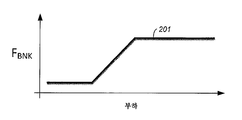
도 3은 본 발명의 실시예에 따른 부하 조건의 함수로서 의사 공진 스위칭(QRS) 블랭킹 주파수를 보여주는 플롯을 도시한다.
도 4는 본 발명의 실시예에 따른 수정된 능동 클램프 모드에서의 도 1의 컨버터의 신호 파형들을 도시한다.
도 5 내지 도 7은 본 발명의 실시예에 따른 상보적인 능동 클램프 모드에서의 도 1의 컨버터의 시뮬레이션 결과들을 도시한다.
도 8은 동일한 음의 전류에 대한 전력 손실의 함수로서 로우 라인 전압 입력 및 하이 라인 전압 입력에서의 스위칭 주파수의 플롯들을 도시한다.
도 9는 본 발명의 실시예에 따른 도 1의 컨버터의 능동 클램프 스위칭 모드들 사이의 전이를 그래프로 보여준다.
도 10은 본 발명의 실시예에 따른 능동 클램프 플라이백(ACF) 제어기를 도시한다.
도 11은 본 발명의 실시예에 따른 ACF 제어기를 도시한다.
도 12는 본 발명의 실시예에 따른 변압기 전압 및 전류의 파형들을 도시한다.
도 13은 본 발명의 실시예에 따른 ACF 제어기를 도시한다.
도 14는 본 발명의 실시예에 따른 도 1의 컨버터의 신호 파형들을 도시한다.
도 15는 본 발명의 실시예에 따른 ACF 제어기를 도시한다.
도 16은 본 발명의 실시예에 따른 도 1의 컨버터의 신호 파형들을 도시한다.
도 17 내지 도 19는 본 발명의 실시예들에 따른 출력 전압 감지 회로들의 개략도를 도시한다.
상이한 도면들에서의 동일한 참조 라벨의 사용은 동일하거나 유사한 컴포넌트들을 지시한다.1 shows an active clamp flyback converter according to an embodiment of the present invention.
Figure 2 shows the signal waveforms of the converter of Figure 1 in a complementary active clamp mode and in a modified active clamp mode according to an embodiment of the present invention.
Figure 3 shows a plot showing the quasi-resonant switching (QRS) blanking frequency as a function of the load condition according to an embodiment of the present invention.
Figure 4 shows the signal waveforms of the converter of Figure 1 in a modified active clamp mode according to an embodiment of the present invention.
5 to 7 show simulation results of the converter of FIG. 1 in a complementary active clamp mode according to an embodiment of the present invention.
Figure 8 shows plots of the switching frequency at the low line voltage input and the high line voltage input as a function of power loss for the same negative current.
Figure 9 graphically illustrates the transition between active clamp switching modes of the converter of Figure 1 according to an embodiment of the present invention.
10 illustrates an active clamp flyback (ACF) controller in accordance with an embodiment of the present invention.
11 shows an ACF controller according to an embodiment of the present invention.
Figure 12 shows waveforms of transformer voltage and current according to an embodiment of the present invention.
13 shows an ACF controller according to an embodiment of the present invention.
Figure 14 shows signal waveforms of the converter of Figure 1 according to an embodiment of the invention.
15 shows an ACF controller according to an embodiment of the present invention.
Figure 16 shows signal waveforms of the converter of Figure 1 according to an embodiment of the invention.
17-19 illustrate schematic diagrams of output voltage sensing circuits in accordance with embodiments of the present invention.
Use of the same reference label in different drawings indicates the same or similar components.
본 개시에서, 본 발명의 실시예들의 철저한 이해를 제공하기 위해, 회로들, 컴포넌트들 및 방법들의 예들과 같은 다수의 특정 세부 사항이 제공된다. 그러나, 당업자는 본 발명이 특정 세부 사항들 중 하나 이상 없이도 실시될 수 있음을 인식할 것이다. 다른 경우들에서, 잘 알려진 세부 사항들은 본 발명의 태양들을 모호하게 하는 것을 피하기 위해 도시되거나 설명되지 않는다.In this disclosure, numerous specific details are provided, such as examples of circuits, components and methods, in order to provide a thorough understanding of embodiments of the invention. However, those skilled in the art will recognize that the invention may be practiced without one or more of the specific details. In other instances, well-known details have not been shown or described in order to avoid obscuring aspects of the present invention.
일반적으로 말해서, 능동 클램프 플라이백 컨버터의 효율은 클램프 스위치와 변압기에서의 높은 RMS(root mean square) 전류에 의해 본질적으로 제한된다. 본 발명의 실시예들에서, RMS 전류는 부하 조건들에 기초하여 컨버터 스위칭 주파수를 변화시킴으로써 능동 클램프 스위칭 모드를 변경하고/하거나 음의 전류를 감소시키는 것에 의해 감소될 수 있다. 능동 클램프 스위칭 모드, 즉 클램프 스위치의 스위칭 알고리즘은 부하 조건들에 기초하여 제1 동작 모드에서 제2 동작 모드로 그리고 반대로 제2 동작 모드에서 제1 동작 모드로 변경될 수 있다. 부하 조건은 출력 전압 피드백 신호로부터 또는 예를 들어 전원 스위치의 드레인-소스 간 전류의 적분으로부터 도출되는 신호로부터 검출될 수 있다. 출력 전압 피드백 신호의 감쇠는 능동 클램프 스위칭 모드에 따라 변경될 수 있다.Generally speaking, the efficiency of the active clamp flyback converter is inherently limited by the high root mean square (RMS) current in the clamp switch and transformer. In embodiments of the present invention, the RMS current may be reduced by changing the active clamp switching mode and / or by reducing the negative current by varying the converter switching frequency based on load conditions. The active clamp switching mode, that is, the switching algorithm of the clamp switch, can be changed from the first operation mode to the second operation mode and vice versa, based on the load conditions, from the second operation mode to the first operation mode. The load condition can be detected from the output voltage feedback signal or from a signal derived, for example, from the integration of the drain-source current of the power switch. The attenuation of the output voltage feedback signal can be varied according to the active clamp switching mode.
도 1은 본 발명의 실시예에 따른 능동 클램프 플라이백 컨버터(100)를 도시한다. 도 1의 예에서, AC 소스는 풀 브리지 정류기(full-bridge rectifier)에 의해 정류되는 입력 전압(VIN)을 제공하고, 입력 커패시터(CIN)가 정류된 입력 전압을 수신한다. 변압기(T1)는 1차 권선(NP), 2차 권선(NS), 및 보조 권선(NA)을 갖는다. 분석 목적으로, 도 1은 변압기(T1)에 의해 관찰되는 자화 인덕턴스(도 1, 자화 인덕턴스 Lm), 자화 전류(도 1, 자화 전류 ILm), 누설 인덕턴스(도 1, 누설 인덕턴스 Llk) 및 누설 전류(도 1, 누설 전류 iLk)를 도시한다.Figure 1 illustrates an active
도 1의 예에서, 컨버터(100)는 전원 스위치로서의 역할을 하는 로우측 스위치(S1)를 갖는다. 일 실시예에서, 로우측 스위치(S1)는 1차 권선(NP)의 제1 단부에 연결된 드레인 및 전류 감지 저항기(RCS)의 제1 단부에 연결된 소스를 갖는 금속 산화물 반도체 전계 효과 트랜지스터(MOSFET)를 포함한다. 전류 감지 저항기(RCS)의 제2 단부는 접지에 연결된다. 2차측에서, 컨버터(100)는 2차 권선(NS)의 제1 단부에 연결된 애노드(anode)와 출력 커패시터(CO)의 제1 단부에 연결된 캐소드(cathode)를 갖는 다이오드 정류기(D1)를 포함한다. 출력 커패시터(CO)의 제2 단부 및 2차 권선(NS)의 제2 단부는 접지에 연결된다. DC 출력 전압(VOUT)은 출력 커패시터(CO)의 양단에 발생된다.In the example of Fig. 1, the
도 1의 예에서, 능동 클램핑은 클램프 커패시터(C2), 및 클램프 스위치로서의 역할을 하는 하이측 스위치(S2)에 의해 제공된다. 일 실시예에서, 하이측 스위치(S2)는 클램프 커패시터(C2)의 제1 단부에 연결된 드레인 및 로우측 스위치(S1)의 드레인에 그리고 1차 권선(NP)의 제1 단부에 연결된 소스를 갖는 MOSFET을 포함한다. 클램프 커패시터(C2)의 제2 단부는 1차 권선(NP)의 제2 단부에 연결된다.In the example of Figure 1, active clamping is provided by clamp capacitor C2 and a high side switch S2 acting as a clamp switch. In one embodiment, the high side switch S2 has a drain connected to the first end of the clamp capacitor C2 and a drain connected to the drain of the low side switch S1 and a source connected to the first end of the primary winding NP MOSFET. The second end of the clamp capacitor C2 is connected to the second end of the primary winding NP.
도 1의 예에서, 능동 클램프 플라이백(ACF) 제어기(101)는 로우측 스위치(S1) 및 하이측 스위치(S2)의 스위칭 동작을 제어한다. 일 실시예에서, ACF 제어기(101)는 하이측 스위치(S2)의 게이트를 구동하기 위한 HG 핀, 로우측 스위치(S1)의 게이트를 구동하기 위한 LG 핀, 감지 저항기(RCS) 상에 발생된 전류 감지 신호를 수신하기 위한 CS 핀, 능동 클램프 스위칭 모드 변경 포인트를 프로그래밍하기 위한 EC 핀, 전압 감지 신호를 수신하기 위한 VS 핀, 전원 전압을 수신하기 위한 VDD 핀, 및 출력 전압 피드백 신호(도 1, VFB)를 수신하기 위한 FB 핀을 포함하는 패키지를 갖는 집적 회로(IC)로서 구현된다. 출력 전압 피드백 신호는 출력 전압(VOUT)을 나타내고, 종래의 피드백 회로 블록(도시되지 않음)을 사용하여 생성될 수 있다. 능동 클램프 스위칭 모드가 제1 모드에서 제2 모드로, 그리고 그 반대로 전이하는 포인트는 EC 핀에 연결된 저항기(REC)의 저항을 선택함으로써 프로그래밍될 수 있다. ACF 제어기(101)는 본 발명의 장점들을 손상시킴이 없이 본 개시에 따른 다양한 아날로그, 디지털, 및/또는 혼합 회로들을 사용하여 구현될 수 있다.In the example of Fig. 1, the active clamp flyback (ACF)
도 1의 예에서, 보조 권선(NA)은 저항 분할기(R1 및 R2) 양단에 보조 전압(VAUX)을 발생시킨다. R2 양단의 전압은 감지 전압으로서 제어기(101)에 의해 수신되고, 이로부터 출력 전압 조건들이 보호 회로 등에 대해 감지될 수 있다. 저항 분할기(R1 및 R2) 양단의 전압은 또한 커패시터(C3) 양단에 전원 전압(VDD)을 발생시키는 데 이용된다.In the example of FIG. 1, the auxiliary winding NA generates an auxiliary voltage V AUX across the resistance dividers R1 and R2. The voltage across R2 is received by the
일 실시예에서, 제어기(101)는 2개의 능동 클램프 스위칭 모드, 즉 상보적인 능동 클램프 모드 및 수정된 능동 클램프 모드 중 하나에 따라 로우측 스위치(S1) 및 하이측 스위치(S2)의 스위칭 동작을 제어한다. 도 2는 본 발명의 실시예에 따른 상보적인 능동 클램프 모드(도 2, 130)에서 그리고 수정된 능동 클램프 모드(도 2, 140)에서의 컨버터(100)의 신호 파형들을 도시한다. 도 2는, 위에서 아래로, 로우측 스위치(S1)로의 로우측 게이트 구동 신호(도 2, LG), 턴 온 데드 타임 신호(도 2, ON_DT), 하이측 스위치(S2)로의 하이측 게이트 구동 신호(도 2, HG), 자화 전류(도 2, iLM), 로우측 스위치(S1)의 드레인-소스 간 전압(도 2, VDS_Lo), 하이측 스위치(S2)의 드레인-소스 간 전압(도 2, VDS_Hi), 및 다이오드 정류기(D1)의 방전(턴 온) 시간(도 2, TD(Tdis))의 파형들을 도시한다.In one embodiment, the
상보적인 능동 클램프 모드(도 2, 130)에서의 신호들을 참조하면, 일 실시예에서, 컨버터(100)의 스위칭 주파수(도 2, FS)는 로우측 스위치(S1)의 스위칭 주파수인 것으로 정의된다. 따라서, 로우측 스위치(S1)는 스위칭 사이클마다, 즉 컨버터(100)의 스위칭 주파수의 1주기(1/FS)에서 한 번 턴 온된다. 그의 이름이 암시하는 바와 같이, 상보적인 능동 클램프 모드에서, 하이측 스위치(S2)는 로우측 스위치(S1)가 오프일 때 온이고, 하이측 스위치(S2)는 로우측 스위치(S1)가 온일 때 오프이다. 하이측 스위치(S2)는 스위칭 사이클마다 한 번 턴 온된다. 하이측 스위치(S2)가 턴 오프될 때, 로우측 스위치(S1)는 턴 온 데드 타임 신호에 의해 지시된 데드 타임 후에 턴 온된다. 자화 전류는 로우측 스위치(S1)가 온일 때 증가하고, 로우측 스위치(S1)가 오프일 때 감소한다. 로우측 스위치(S1)가 오프일 때, 1차 권선(NP)으로부터의 전류는 하이측 스위치(S2)의 바디 다이오드를 통해 흘러 클램프 커패시터(C2)(도 1 참조)를 충전하고 클램프 전압(도 1, VCLAMP)을 발생시킨다. 하이측 스위치(S2)는 로우측 스위치(S1)가 턴 오프된 후 데드 타임 후에 턴 온된다. 일 실시예에서, 개선된 효율을 위해, 컨버터(100)의 스위칭 주파수는 상보적인 능동 클램프 모드에서 부하 조건에 기초하여 자동으로 조정된다. 컨버터(100)의 스위칭 주파수는 부하가 감소함에 따라 증가하고, 부하가 증가함에 따라 감소한다. 컨버터(100)는 바람직하게는 중부하 조건들 동안에는 상보적인 능동 클램프 모드에 놓인다.Referring to the signals in the complementary active clamp mode (Figure 2, 130), in one embodiment, the switching frequency (Figure 2, FS) of
수정된 능동 클램프 모드(도 2, 140)에서의 신호들을 참조하면, 로우측 스위치(S1)는 상보적인 능동 클램프 모드에서와 같이 턴 온 및 턴 오프된다. 주된 차이점은, 수정된 능동 클램프 모드에서는, 하이측 스위치(S2)가 컨버터(100)의 스위칭 사이클마다 두 번 턴 온된다는 것이다. 따라서, 일 실시예에서, 하이측 스위치(S2)로의 하이측 게이트 구동 신호는 스위칭 사이클마다 2개의 펄스를 갖는다. 로우측 스위치(S1)가 턴 오프될 때, 로우측 스위치(S1)의 드레인-소스 간 전압은 증가하며, 이때 하이측 게이트 구동 신호의 제1 펄스(도 2, 161)는 하이측 스위치(S2)의 드레인-소스 간 전압이 제로가 될 때 발생된다(즉, 제로 전압 스위칭(ZVS)). 하이측 게이트 구동 신호의 제2 펄스(도 2, 162)는 의사 공진 스위칭(QRS)에 의해, QRS 블랭킹 시간의 만료 후에 발생된다. 하이측 게이트 구동 신호의 제1 및 제2 펄스의 펄스 폭은 미리 설정되거나 적응적으로 설정될 수 있다. 일부 실시예들에서, 하이측 게이트 구동 신호의 제2 펄스의 펄스 폭은 컨버터(100)의 듀티 사이클에 기초하여 적응적으로 설정된다. 도 2의 예에서, 하이측 게이트 구동 신호의 제2 펄스는 QRS 블랭킹 시간의 만료 후에 로우측 스위치(S1)의 드레인-소스 간 전압의 피크에서 발생된다. 일 실시예에서, 개선된 효율을 위해, QRS 블랭킹 시간은 부하 조건에 기초하여 자동으로 조정된다. QRS 블랭킹 시간은 부하가 감소함에 따라 증가될 수 있고(즉, 더 길게 만들어질 수 있고), 부하가 증가함에 따라 감소될 수 있다(즉, 더 짧게 만들어질 수 있다). 컨버터(100)는 바람직하게는 중간 및 경부하 조건들 동안에는 수정된 능동 클램프 모드에 놓인다.Referring to the signals in the modified active clamp mode (FIG. 2, 140), the low side switch S1 is turned on and off as in the complementary active clamp mode. The main difference is that, in the modified active clamp mode, the high side switch S2 is turned on twice per switching cycle of the
도 3은 본 발명의 실시예에 따른 부하 조건의 함수로서 QRS 블랭킹 주파수(FBNK)를 보여주는 플롯(201)을 도시한다. 도 3의 예에서, QRS 블랭킹 시간, 즉 1/FBNK는 중부하 조건들에서는 더 짧고, 경부하 조건들에서는 더 길다. 잘 알려진 바와 같이, 부하가 컨버터로부터 다량의 전류를 끌어낼 때는 부하는 중부하이고, 부하가 컨버터로부터 소량의 전류를 끌어낼 때는 부하는 경부하이다. QRS 블랭킹 시간은 의사 공진 스위칭에 의한 하이측 스위치(S2)의 턴 온이 디스에이블되는 기간이다. 즉, 하이측 스위치(S2)는 QRS 블랭킹 시간 동안 의사 공진 스위칭에 의해 턴 온될 수 없다.Figure 3 shows a
설명된 바와 같이, 수정된 능동 클램프 모드에서는, 하이측 게이트 구동 신호의 제2 펄스는 의사 공진 스위칭에 의해 어서트된다. 일반적으로 말해서, 의사 공진 스위칭은 상보적인 스위칭에 비하여 더 낮은 도통 손실을 야기한다. 그러나, 부하가 감소함에 따라, 스위칭 손실의 비율이 증가한다. 따라서, 개선된 효율을 위해, 도 3에 도시된 바와 같이 부하가 감소할 때 QRS 블랭킹 시간이 증가된다(즉, QRS 블랭킹 주파수(FBNK)가 감소된다). 플롯(201)은 수정된 능동 클램프 모드에서의 조정 가능한 QRS 블랭킹 시간 특징의 일반적인 예시를 위해 제공된다는 점에 유의해야 한다. 더 구체적으로, 플롯(201)은 중부하 조건들 동안에 반드시 평탄한 응답을 갖지는 않는다.As described, in the modified active clamp mode, the second pulse of the high side gate drive signal is asserted by pseudo resonance switching. Generally speaking, pseudo-resonant switching causes lower conduction losses compared to complementary switching. However, as the load decreases, the ratio of switching losses increases. Thus, for improved efficiency, the QRS blanking time is increased (i.e., the QRS blanking frequency F BNK is reduced) as the load decreases, as shown in FIG. It should be noted that
도 4는 본 발명의 실시예에 따른 수정된 능동 클램프 모드에서의 컨버터(100)의 신호 파형들을 도시한다. 도 4는 로우측 스위치(S1)로의 로우측 게이트 구동 신호(도 4, LG), 하이측 스위치(S2)로의 하이측 게이트 구동 신호(도 4, HG), 및 로우측 스위치(S1)의 드레인-소스 간 전압(도 4, VDS_Lo)의 세부 사항들을 도시한다. 로우측 게이트 구동 신호가 디어서트되면, 로우측 스위치(S1)가 턴 오프되어, 로우측 스위치(S1)의 드레인-소스 간 전압이 증가하게 된다. 하이측 스위치(S2)의 ZVS에서 발생하는, 로우측 스위치(S1)의 드레인-소스 간 전압의 제1 피크에서, 하이측 게이트 구동 신호의 제1 펄스(P1)가 발생된다. 하이측 스위치(S2)가 턴 오프된 후 어떤 포인트에서, 로우측 스위치(S1)의 드레인-소스 간 전압이 발진하기 시작한다. 하이측 스위치(S2)는 QRS 블랭킹 시간(도 4, TBNK) 동안 턴 온되는 것이 디스에이블된다. QRS 블랭킹 시간의 만료 후에 로우측 스위치(S1)의 드레인-소스 간 전압의 피크가 발생할 때, 하이측 게이트 구동 신호의 제2 펄스(P2)가 발생된다. 설명된 바와 같이, QRS 블랭킹 시간은 수정된 능동 클램프 모드에서의 부하 조건들에 기초하여 적응적으로 조정될 수 있다.4 shows signal waveforms of
도 5 내지 도 7은 본 발명의 실시예에 따른 상보적인 능동 클램프 모드에서의 컨버터(100)의 시뮬레이션 결과들을 도시한다. 도 5 내지 도 7의 시뮬레이션 결과들은 0.5 옴의 드레인-소스 간 온 저항(Rdson)을 갖는 하이측 스위치(S2) 및 2 Ω 저항을 갖는 1차 권선(NP)을 가정한다. 도 5 내지 도 7에서, 상부 파형(플롯 211)은 하이측 스위치(S2)의 드레인-소스 간 전류 IDS에 대한 것이고, 하부 파형들은 자화 전류(플롯 212) 및 음의 전류(플롯 213)에 대한 것들이다. 도 5는 250 ㎑ 스위칭 주파수, 484 mA RMS의 하이측 스위치(S2) 전류, 540 mA RMS의 자화 전류, 및 780 mW의 총 전력 손실(대략 3% 손실)에서의 최대 부하에 대한 시뮬레이션 결과들을 도시한다. 도 6은 250 ㎑ 스위칭 주파수, 423 mA RMS의 하이측 스위치(S2) 전류, 426 mA RMS의 자화 전류, 및 580 mW의 총 전력 손실(대략 4.6% 손실)에서의 50% 부하(즉, 정격 부하의 절반)에 대한 시뮬레이션 결과들을 도시한다. 도 7은 400 ㎑ 스위칭 주파수, 283 mA RMS의 하이측 스위치(S2) 전류, 320 mA RMS의 자화 전류, 및 270 mW의 총 전력 손실(대략 2.2% 손실)에서의 50% 부하에 대한 시뮬레이션 결과들을 도시한다. 도 5 내지 도 7의 시뮬레이션 결과들은 스위칭 주파수를 증가시킴으로써 RMS 전류가 감소될 수 있음을 나타낸다. 도 5 내지 도 7의 시뮬레이션 결과들은 도 8의 플롯들(231 및 232)에서와 같이 요약될 수 있다. 도 8은 동일한 음의 전류에 대한 전력 손실의 함수로서 로우 라인 전압 입력에서의 스위칭 주파수(플롯(231)) 및 하이 라인 전압 입력에서의 스위칭 주파수(플롯(232))의 플롯들을 도시한다. 도 8에 도시된 바와 같이, 동일한 음의 전류에 대한 스위칭 주파수를 증가시키면 전력 손실이 감소된다.5-7 illustrate simulation results of the
도 9는 본 발명의 실시예에 따른 컨버터(100)의 능동 클램프 스위칭 모드들 사이의 전이를 그래프로 도시한다. 도 9의 예에서, 컨버터(100)는 모드 변경 포인트의 오른쪽으로는 상보적인 능동 클램프 모드(플롯(234))에 따라 능동 클램프 스위칭을 수행하고, 모드 변경 포인트의 왼쪽으로는 수정된 능동 클램프 모드(플롯(233))에 따라 능동 클램프 스위칭을 수행한다. 모드 변경 포인트는 정격 부하의 함수로서 선택될 수 있다. 일 실시예에서, 사용자는 컨버터(100)가 능동 클램프 모드에서 수정된 클램프 모드로 그리고 그 반대로 전이할 특정 부하 백분율을 프로그래밍할 수 있다(화살표 235 참조). 더 구체적으로, 컨버터(100)는 부하가 모드 변경 포인트 아래로 감소할 때는 상보적인 능동 클램프 스위칭에서 수정된 능동 클램프 스위칭으로 전이하고, 부하가 모드 변경 포인트 위로 증가할 때는 수정된 능동 클램프 모드에서 상보적인 능동 클램프 모드로 전이한다. 설명된 바와 같이, 상보적인 능동 클램프 모드에서는, 컨버터(100)의 스위칭 주파수(도 9, FS)는 부하가 증가함에 따라 감소되고 반대로 부하가 감소함에 따라 증가된다; 수정된 능동 클램프 모드에서는, QRS 블랭킹 시간(도 9, QRS 블랭킹 주파수(FBNK)의 역수)은 부하가 감소함에 따라 증가되고 반대로 부하가 증가함에 따라 감소된다. 부하 조건은 컨버터(100)의 출력 전압을 나타내는 출력 전압 피드백 신호로부터 또는 컨버터(100)의 출력 전력으로부터 검출될 수 있다.FIG. 9 graphically illustrates the transition between active clamp switching modes of
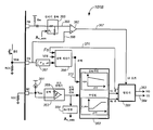
도 10은 본 발명의 실시예에 따른 ACF 제어기(101A)를 도시한다. ACF 제어기(101A)는 도 1의 ACF 제어기(101)의 특정 실시예이며, 여기서 상보적인 능동 클램프 모드에서의 컨버터(100)의 스위칭 주파수 또는 수정된 능동 클램프 모드에서의 QRS 블랭킹 주파수는 출력 전압을 나타내는 출력 전압 피드백 신호(도 10, VFB)에 기초하여 조정된다. 또한 ACF 제어기(101A)에서, 능동 클램프 스위칭 모드는 출력 전압 피드백 신호에 기초하여 선택된다. 이해될 수 있는 바와 같이, 출력 전압은 부하 조건에 대한 정보를 가지며, 고 부하 조건들에서는 낮아지는 경향이 있고 저 부하 조건들에서 높아지는 경향이 있다.10 shows an
도 10의 예에서, ACF 제어기(101A)는 발진기 블록(301), 능동 클램프 모드 블록(302), 모드 선택기 블록(303), 이득 변경 블록(304), 및 감쇠기 블록(305)을 포함한다. 이해될 수 있는 바와 같이, ACF 제어기(101A)의 회로 블록들은 본 발명의 장점들을 손상시킴이 없이 아날로그, 디지털, 또는 혼합 회로들을 사용하여 구현될 수 있다. 일반적으로 말해서, ACF 제어기(101A)는 다양한 회로들을 사용하여 본 명세서에서 제공된 파형들 및 설명들에 따라 구현될 수 있다.In the example of FIG. 10, the
도 10의 예에서, 발진기 블록(301)은, 어느 능동 클램프 스위칭 모드가 현재 선택되는지에 따라, 상보적인 능동 클램프 모드(도 2, 130 참조)에 따라 또는 수정된 능동 클램프 모드(도 2, 140 참조)에 따라 하이측 스위치(S2)를 구동하기 위한 하이측 게이트 구동 신호(도 10, 313) 및 로우측 스위치(S1)를 구동하기 위한 로우측 게이트 구동 신호(도 10, 314)를 생성하도록 구성된다. 하이측 및 로우측 게이트 구동 신호들은 직접 또는 다른 회로를 통해(예를 들어, 추가 처리를 위해), 각각, 하이측 스위치(S2) 및 로우측 스위치(S1)에 제공될 수 있다.In the example of FIG. 10, the
도 10의 예에서, 발진기 블록(301)은 로우측 스위치(S1)를 턴 오프하는 것을 지시하는 LG 오프 신호, 로우측 스위치(S1)를 턴 온하는 것을 지시하는 LG 온 신호, 및 하이측 스위치(S2)를 턴 온하는 것을 지시하는 HG 온 신호를 수신한다. 발진기 블록(301)은 LG 오프, LG 온, 및 HG 온 신호들에 따라 하이측 및 로우측 게이트 구동 신호들을 어서트/디어서트시킨다. 하이측 게이트 구동 신호는 HG 온 신호가 디어서트될 때 디어서트될 수 있으며; 따라서, 하이측 게이트 구동 신호는 반드시 별도의 신호에 의해 능동적으로 턴 오프될 필요는 없다는 점에 유의해야 한다.10, the
도 10의 예에서, 능동 클램프 모드 블록(302)은 상보적인 능동 클램프 모드 또는 수정된 능동 클램프 모드 중 어느 것이 현재 선택되든지 그에 따라 LG 온 및 HG 온 신호들을 생성하도록 구성된다. 능동 클램프 모드 블록(302)은 모드 선택기 블록(303)으로부터 수신된 모드 선택 신호(도 10, 315)에 따라 상보적인 능동 클램프 모드 또는 수정된 능동 클램프 모드에 대해 설정된다. 능동 클램프 모드 블록(302)은 부하 조건에 대해 알려주는, 출력 전압 피드백 신호(도 10, 316)를 수신하여, 상보적인 능동 클램프 모드에서의 컨버터(100)의 스위칭 주파수 또는 수정된 능동 클램프 모드에서의 QRS 블랭킹 시간을 조정한다.In the example of FIG. 10, the active
상보적인 능동 클램프 모드가 모드 선택기 블록(303)으로부터의 모드 선택 신호에 따라 선택될 때, 능동 클램프 모드 블록(302)은 출력 전압 피드백 신호에 의해 지시된 바와 같은 부하 조건에 따라 LG 온 신호를 생성한다. 더 구체적으로, 능동 클램프 모드 블록(302)은 부하가 증가할 때 감소되고 부하가 감소할 때 증가되는 주파수에서 LG 온 신호를 어서트시킨다. 능동 클램프 모드 블록(302)은 LG 온 신호가 디어서트될 때 데드 타임 후에 HG 온 신호를 어서트시킨다.When a complementary active clamp mode is selected in accordance with the mode selection signal from the
수정된 능동 클램프 모드가 모드 선택기 블록(303)으로부터의 모드 선택 신호에 따라 선택될 때, 일 실시예에서, 능동 클램프 모드 블록(302)은 처음에 하이측 스위치(S2)의 ZVS에 따라 스위칭 사이클 동안에 그리고 두 번째로 QRS 블랭킹 시간(도 4, TBNK)의 만료 후에 하이측 스위치(S2)의 QRS에 따라 스위칭 사이클 동안에 HG 온 신호를 어서트시킨다. 설명된 바와 같이, QRS 블랭킹 시간은 출력 전압 피드백 신호에 의해 지시된 바와 같은 부하 조건에 따라 조정된다. 능동 클램프 모드 블록(302)은 내부적으로 QRS 블랭킹 시간을 생성할 수 있다. 능동 클램프 모드 블록(302)은 부하가 감소할 때 QRS 블랭킹 시간을 길게 하고 부하가 증가할 때 QRS 블랭킹 시간을 단축시킬 수 있다. 능동 클램프 모드 블록(302)은 스위칭 사이클에서 HG 온 신호의 두 번째 어서션(assertion)의 끝에서 데드 타임 후에 LG 온 신호를 생성한다.When the modified active clamp mode is selected in accordance with the mode selection signal from the
도 10의 예에서, 전류원(311)은 능동 클램프 모드 블록(302)이 능동 클램프 스위칭 모드들을 변경하는 모드 변경 포인트를 사용자가 프로그래밍하는 것을 허용하도록 저항기(REC) 상에 전압을 발생시킨다. 모드 선택기 블록(303)은 EC 핀 상의 전압을 FB 핀 상의 출력 전압 피드백 신호와 비교하여 (출력 전압 피드백 신호에 의해 지시된 바와 같은) 부하 조건에 기초하여 능동 클램프 스위칭 모드를 자동으로 선택하고, 그에 따라 모드 선택 신호를 생성한다. 모드 선택 신호는 능동 클램프 모드 블록(302)에 제공되고(도 10, 315 참조) 이득 변경 블록(304)에 제공된다(도 10, 317 참조). 이득 변경 블록(304)은 능동 클램프 스위칭 모드에 따라 출력 전압 피드백 신호를 감쇠시키기 위해 감쇠기 블록(305)의 이득을 변경한다. 이는 유리하게도 능동 클램프 스위칭 모드 전이에 의해 야기되는 출력 전압 오버슈트를 제한한다. 증폭기(312)는 감쇠된 출력 전압 피드백 신호(도 10, 318)를 CS 핀 상의 전류 감지 신호(도 10, 319)와 비교하여 로우측 스위치(S1)를 턴 오프하는 LG 오프 신호(도 10, 320)를 생성한다.In the example of FIG. 10, the
도 11은 본 발명의 실시예에 따른 ACF 제어기(101B)를 도시한다. ACF 제어기(101B)는 도 1의 ACF 제어기(101)의 특정 실시예이며, 여기서 상보적인 능동 클램프 모드에서의 컨버터(100)의 스위칭 주파수 또는 수정된 능동 클램프 모드에서의 QRS 블랭킹 주파수는 컨버터(100)의 출력 전력에 기초하여 조정된다. ACF 제어기(101B)에서, 능동 클램프 스위칭 모드는 또한 출력 전력에 기초하여 선택된다.11 shows an
도 11의 예에서, ACF 제어기(101B)는 발진기 블록(351), 능동 클램프 모드 블록(352), 모드 선택기 블록(353), 이득 변경 블록(354), 감쇠기 블록(355), 전력 계산기 블록(356), 및 적분 블록(357)을 포함한다. 이해될 수 있는 바와 같이, ACF 제어기(101B)의 회로 블록들은 본 발명의 장점들을 손상시킴이 없이 아날로그, 디지털, 또는 혼합 회로들을 사용하여 구현될 수 있다. 일반적으로 말해서, ACF 제어기(101B)는 다양한 회로들을 사용하여 본 명세서에서 제공된 파형들 및 설명들에 따라 구현될 수 있다.11, the
도 11의 예에서, 발진기 블록(351)은, 어느 능동 클램프 스위칭 모드가 현재 선택되는지에 따라, 상보적인 능동 클램프 모드(도 2, 130 참조)에 따라 또는 수정된 능동 클램프 모드(도 2, 140 참조)에 따라 하이측 스위치(S2)를 구동하기 위한 하이측 게이트 구동 신호(도 11, 363) 및 로우측 스위치(S1)를 구동하기 위한 로우측 게이트 구동 신호(도 11, 364)를 생성하도록 구성된다. 하이측 및 로우측 게이트 구동 신호들은 직접 또는 다른 회로를 통해, 각각, 하이측 스위치(S2) 및 로우측 스위치(S1)에 제공될 수 있다. 도 11의 예에서, 발진기 블록(351)은 컨버터(100)의 스위칭 주파수를 지시하는, 로우측 스위치(S1)의 스위칭 주파수를 지시하는 스위칭 주파수 신호(도 11, 371)를 생성한다.11, the
발진기 블록(351)은 로우측 스위치(S1)를 턴 오프하는 것을 지시하는 LG 오프 신호, 로우측 스위치(S1)를 턴 온하는 것을 지시하는 LG 온 신호, 및 하이측 스위치(S2)를 턴 온하는 것을 지시하는 HG 온 신호를 수신한다. 발진기 블록(351)은 LG 오프, LG 온, 및 HG 온 신호들에 따라 하이측 및 로우측 게이트 구동 신호들을 어서트/디어서트시킨다. 하이측 게이트 구동 신호는 HG 온 신호가 디어서트될 때 디어서트될 수 있으며; 따라서, 하이측 게이트 구동 신호는 반드시 별도의 신호에 의해 능동적으로 턴 오프될 필요는 없다는 점에 유의해야 한다.The
도 11의 예에서, 능동 클램프 모드 블록(352)은 상보적인 능동 클램프 모드 또는 수정된 능동 클램프 모드 중 어느 것이 현재 선택되든지 그에 따라 LG 온 및 HG 온 신호들을 생성하도록 구성된다. 능동 클램프 모드 블록(352)은 모드 선택기 블록(353)으로부터 수신된 모드 선택 신호에 따라 상보적인 능동 클램프 모드 또는 수정된 능동 클램프 모드에 대해 설정된다. 능동 클램프 모드 블록(352)은 부하 조건에 대해 알려주는, 컨버터(100)의 출력 전력을 나타내는 출력 전력 신호(도 11, 372)를 수신하여, 상보적인 능동 클램프 모드에서의 컨버터(100)의 스위칭 주파수 또는 수정된 능동 클램프 모드에서의 QRS 블랭킹 시간을 조정한다.In the example of FIG. 11, the active
상보적인 능동 클램프 모드가 모드 선택기 블록(353)으로부터의 모드 선택 신호에 따라 선택될 때, 능동 클램프 모드 블록(352)은 전력 계산기 블록(356)으로부터 수신된 출력 전력 신호에 의해 지시된 바와 같은 부하 조건에 따라 LG 온 신호를 생성한다. 더 구체적으로, 능동 클램프 모드 블록(352)은 부하가 증가할 때 감소되고 부하가 감소할 때 증가되는 주파수에서 LG 온 신호를 어서트시킨다. 능동 클램프 모드 블록(352)은 LG 온 신호가 디어서트될 때 데드 타임 후에 HG 온 신호를 어서트시킨다.When a complementary active clamp mode is selected in accordance with the mode selection signal from the
수정된 능동 클램프 모드가 모드 선택기 블록(353)으로부터의 모드 선택 신호에 따라 선택될 때, 일 실시예에서, 능동 클램프 모드 블록(352)은 처음에 하이측 스위치(S2)의 ZVS에 따라 스위칭 사이클 동안에 그리고 두 번째로 QRS 블랭킹 시간(도 4, TBNK)의 만료 후에 하이측 스위치(S2)의 QRS에 따라 스위칭 사이클 동안에 HG 온 신호를 어서트시킨다. 설명된 바와 같이, 수정된 능동 클램프 모드에서, QRS 블랭킹 시간은, ACF 제어기(101B)에서 출력 전력 신호에 의해 지시되는 부하 조건에 따라 조정된다. 능동 클램프 모드 블록(352)은 내부적으로 QRS 블랭킹 시간을 생성할 수 있다. 능동 클램프 모드 블록(352)은 부하가 감소할 때 QRS 블랭킹 시간을 길게 하고 부하가 증가할 때 QRS 블랭킹 시간을 단축시킬 수 있다. 능동 클램프 모드 블록(352)은 스위칭 사이클에서 HG 온 신호의 두 번째 어서션의 끝에서 데드 타임 후에 LG 온 신호를 생성한다.When the modified active clamp mode is selected according to the mode selection signal from the
도 11의 예에서, 전류원(361)은 능동 클램프 모드 블록(352)이 능동 클램프 스위칭 모드들을 변경하는 모드 변경 포인트를 사용자가 프로그래밍하는 것을 허용하도록 저항기(REC) 상에 전압을 발생시킨다. 모드 선택기 블록(353)은 EC 핀 상의 전압을 출력 전력 신호(도 11, 368)와 비교하여 부하 조건에 기초하여 능동 클램프 스위칭 모드를 자동으로 선택하고, 그에 따라 모드 선택 신호를 생성한다. 모드 선택기 블록(353)은 모드 선택 신호를 능동 클램프 모드 블록(352)에 그리고 이득 변경 블록(354)에 제공한다. 이득 변경 블록(354)은 능동 클램프 스위칭 모드에 따라 FB 핀 상에서 수신된 출력 전압 피드백 신호를 감쇠시키기 위해 감쇠기 블록(355)의 이득을 변경한다. 이는 유리하게도 능동 클램프 스위칭 모드 전이에 의해 야기되는 출력 전압 오버슈트를 제한한다. 증폭기(362)는 감쇠된 출력 전압 피드백 신호(도 11, 365)를 CS 핀 상의 전류 감지 신호(도 11, 366)와 비교하여 로우측 스위치(S1)를 턴 오프하는 LG 오프 신호(도 11, 367)를 생성한다.In the example of Figure 11, the
도 11의 예에서, CS 핀은 로우측 스위치(S1)의 드레인 전류에 의해 발생된 전류 감지 전압(도 11, VCS)을 수신한다. 적분 블록(357)은 전류 감지 전압을 적분하고 적분된 전류 감지 전압을 전력 계산기 블록(356)에 제공한다. 이해될 수 있는 바와 같이, 컨버터(100)의 출력 전력은 다음과 같이 기술될 수 있으며,In the example of Fig. 11, the CS pin receives the current sense voltage (Fig. 11, VCS) generated by the drain current of the low side switch S1. The
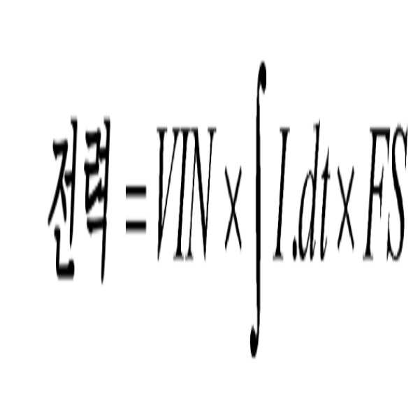
여기서, VIN은 입력 라인 전압이고, FS는 로우측 스위치(S1)의(또한 컨버터(100)의) 스위칭 주파수이고, I는 로우측 스위치(S1)의 드레인 전류이다. 전력 계산기 블록(356)은 입력 라인 전압(VIN), 스위칭 주파수 신호, 및 적분 블록(357)으로부터의 드레인 전류의 적분을 수신하여 출력 전력을 추정하고 능동 클램프 모드 블록(352)에 제공되고(도 11, 372 참조) 모드 선택기 블록(353)에 제공되는(도 11, 368 참조) 대응하는 출력 전력 신호를 생성한다.Here, VIN is the input line voltage, FS is the switching frequency of the low side switch S1 (also the converter 100), and I is the drain current of the low side switch S1. The
일반적으로 말해서, 하이측 스위치(S2)의 온 시간 동안 충분한 음의 전류를 확보함으로써 로우측 스위치(S1)의 ZVS가 행해질 수 있다. 음의 전류는 ZVS 지연 시간에 의해 제어될 수 있으며; ZVS 지연 시간 후에 로우측 스위치(S1)가 턴 온된다. 일 실시예에서, ZVS 지연 시간은 수정된 능동 클램프 모드에서의 하이측 게이트 구동 신호의 제2 펄스(도 2, 162)의 펄스 폭이다.Generally speaking, ZVS of the low-side switch S1 can be performed by securing a sufficient negative current during the ON time of the high-side switch S2. The negative current can be controlled by the ZVS delay time; After the ZVS delay time, the low side switch S1 is turned on. In one embodiment, the ZVS delay time is the pulse width of the second pulse (Figure 2, 162) of the high side gate drive signal in the modified active clamp mode.
ZVS 지연 시간은 내부 인덕터-커패시터(LC) 지연 및 이 예에서 로우측 스위치(S1)의 듀티 사이클인, 컨버터(100)의 듀티 사이클로부터 결정될 수 있다. LC 지연 시간은 미리 설정될 수 있고 ZVS 지연 시간은 듀티 사이클에 따라 적응적으로 변경될 수 있다. 로우측 스위치(S1)와 하이측 스위치(S2)의 스위칭 사이의 데드 타임은 ZVS 동작을 달성하도록 제어될 수 있다.The ZVS delay time can be determined from the duty cycle of
음의 전류는 다음 수학식으로부터 결정될 수 있으며,The negative current can be determined from the following equation,


여기서, Vin은 입력 전압이고, Vo는 출력 전압이고, n은 변압기의 권선비이고, Ceq는 등가 커패시턴스이고, Ineg는 음의 전류이고, Lm은 자화 인덕턴스이다. 이어서 다음과 같이 된다,Where V in is the input voltage, Vo is the output voltage, n is the turns ratio of the transformer, C eq is the equivalent capacitance, I neg is the negative current, and L m is the magnetizing inductance. Then,


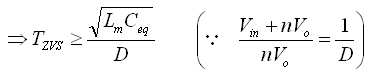

수학식 7에 의해 나타난 바와 같이, ZVS 지연 시간(TZVS)은 로우측 스위치(S1)의 듀티 사이클(D) 및 시간 지연(TD)에 기초하여 적응적으로 설정될 수 있다. 시간 지연(TD)은 제조 중에 (LC 지연 시간에 의해) 또는 사용자에 의해 미리 설정될 수 있어, ZVS 지연 시간이 로우측 스위치(S1)의 듀티 사이클에 의해 좌우되도록 허용할 수 있다.As shown by equation (7), the ZVS delay time (T ZVS ) can be adaptively set based on the duty cycle (D) and the time delay (T D ) of the low side switch (S1). The time delay T D can be preset during manufacture (by LC delay time) or by the user, allowing the ZVS delay time to be dependent on the duty cycle of the low side switch Sl.
도 12는 본 발명의 실시예에 따른 컨버터(100)의 변압기(T1)의 전압(플롯(401)) 및 전류(플롯(402))를 도시한다. 도 12에 도시된 바와 같이, 입력 전압(VIN)을 1차 권선(NP)에 인가하면 자화 전류가 증가한다. 자화 전류(즉, 플롯(402))는 입력 전압(VIN)이 1차 권선(NP)으로부터 제거될 때 감소한다. ZVS 지연 시간(도 12, TZVS)은 자화 전류의 제로 크로싱에서 시작된다. ZVS 지연 시간은, 변압기(T1)가 로우측 스위치(S1)의 ZVS를 허용하기에 충분한 음의 전류(도 12, Ineg)를 형성하도록, 로우측 스위치(S1)의 듀티 사이클에 기초하여 적응적으로 설정된다.12 shows the voltage (plot 401) and current (plot 402) of the transformer T1 of the
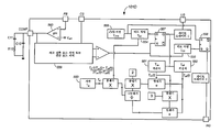
도 13은 본 발명의 실시예에 따른 ACF 제어기(101C)의 개략도를 도시한다. ACF 제어기(101C)는 도 1의 ACF 제어기(101)의 특정 구현이다. 도 13의 예에서, ACF 제어기(101C)는 선택 가능한 능동 클램프 스위칭 모드들을 갖지 않는다. 다른 실시예들에서, 하이측 게이트 구동 신호의 제2 펄스의 펄스 폭을 수정된 능동 클램프 모드에서 설정하기 위해 ACF 제어기(101C)의 특징들이 ACF 제어기(101A(도 10) 또는 101B(도 11))에 통합된다. 이해될 수 있는 바와 같이, 로우측 스위치(S1)의 ZVS에 관한 본 개시의 특징들이 본 발명의 장점들을 손상시킴이 없이 다양한 능동 클램프 플라이백 컨버터들에 통합될 수 있다.13 shows a schematic diagram of an
도 13의 예에서, 로우측 스위치(S1)의 듀티 사이클을 검출하기 위해 로우측 스위치(S1)의 온 시간(도 13, 501) 및 오프 시간(도 13, 502)을 측정하기 위해 카운터들이 이용된다. 듀티 사이클의 역수를 시간 지연(TD)(도 13, 503)과 곱하여 ZVS 지연 시간(도 13, 504)을 생성한다. 시간 지연(TD)은 프로그래밍 등을 위해 외부 컴포넌트들이 연결될 수 있는 추가 핀을 제공하는, ACF 제어기(101C) 집적 회로의 제조 동안의 트리밍에 의해 미리 설정될 수 있다. 일 실시예에서, ZVS 지연 시간은 로우측 스위치(S1)의 드레인-소스 간 전압이 그의 피크에 도달할 때 시작된다. ZVS 지연 시간 만료 후의 데드 타임(도 13, 505) 후에, 로우측 스위치(S1)는 플립-플롭(506)을 세트함으로써 턴 온된다.13, counters are used to measure the on-time (Fig. 13, 501) and the off-time (Fig. 13, 502) of the low-side switch S1 in order to detect the duty cycle of the low- do. The reciprocal of the duty cycle is multiplied by the time delay (T D ) (FIG. 13, 503) to generate the ZVS delay time (FIG. 13, 504). The time delay T D may be preset by trimming during fabrication of the
도 13의 예에서, ACF 제어기(101C)는 외부 커패시터들(C10 및 C11) 및 외부 저항기(R10)를 사용하여 컨버터(100)의 보상을 설정하기 위한 COMP 핀을 포함한다. FB 핀은 오류 증폭기(510)에 의해 기준 전압과 비교되는 출력 전압 피드백 신호를 수신한다. 로우측 스위치(S1)는 플립-플롭(506)을 리셋함으로써 피크 전류 모드 제어 또는 전압 모드 제어(도 13, 509)에 따라 턴 오프될 수 있다. 로우측 스위치(S1)가 턴 오프될 때, 하이측 스위치(S2)는 플립-플롭(508)을 세트함으로써 데드 타임(도 13, 507) 후에 턴 온된다.13, the
도 14는 본 발명의 실시예에 따른 컨버터(100)의 신호 파형들을 도시한다. 도 14는 로우측 스위치(S1)의 드레인 전압(플롯(531)), 변압기(T1)의 전압(플롯(532)), 및 변압기(T1)의 전류(플롯(533))를 도시한다. 도 14의 예에서, 데드 타임(TDT)은 로우측 스위치(S1)의 드레인 전압의 피크로부터 로우측 스위치(S1)의 드레인 및 소스 양단의 제로 전압(즉, ZVS)까지의 기간이고, 데드 타임(TDT1)은 변압기의 음의 전류가 크게 변하지 않는 기간이며, 데드 타임(TDT2)은 변압기 전류가 선형적으로 증가하는 것으로 간주될 수 있는 기간이다. 데드 타임(TDT)은 ZVS 조건을 충족시키기 위해 로우측 스위치(S1)를 턴 온하기 전의 데드 타임이라는 점에 유의한다. ZVS를 수행하기 위해서는, 변압기 전류가 제로에 도달하기 전에 로우측 스위치(S1)의 드레인 전압이 제로에 도달해야 한다. 즉,14 shows signal waveforms of


이다.to be.
변압기 전압 파형(도 14, 532)으로부터,From the transformer voltage waveforms (Figures 14 and 532)

이고 TDT에 대해 풀면And solves for T DT


이다.to be.
수학식 13은 로우측 스위치(S1)의 정확한 ZVS를 허용하는, 데드 타임(TDT)에 대한 적절한 값을 결정하는 수학식을 제공한다. 자화 인덕턴스(Lm) 및 등가 커패시턴스(Ceq)는 알려져 있거나 미리 설정될 수 있기 때문에, 정확한 ZVS를 제공하는 데드 타임은 로우측 스위치(S1)의 온(Ton) 및 오프(Toff) 시간들로부터 적응적으로 설정될 수 있다.Equation (13) provides a mathematical expression for determining an appropriate value for the dead time (T DT ), which allows the correct ZVS of the low
도 15는 본 발명의 실시예에 따른 ACF 제어기(101D)의 개략도를 도시한다. ACF 제어기(101D)는 도 1의 ACF 제어기(101)의 특정 구현이다. 도 15의 예에서, ACF 제어기(101D)는 선택 가능한 능동 클램프 스위칭 모드들을 갖지 않는다. 다른 실시예들에서, 로우측 스위치(S1)의 정확한 ZVS를 위해 로우측 스위치(S1)를 턴 온하기 전에 데드 타입을 설정하기 위해 ACF 제어기(101C)의 특징들이 ACF 제어기(101A(도 10), 101B(도 11), 또는 101C(도 13))에 통합된다. 이해될 수 있는 바와 같이, ZVS를 위한 적응적 데드 타임에 관한 본 개시의 특징들이 본 발명의 장점들을 손상시킴이 없이 다양한 능동 클램프 플라이백 컨버터들에 통합될 수 있다.15 shows a schematic diagram of an ACF controller 101D according to an embodiment of the present invention. The ACF controller 101D is a specific implementation of the
도 15의 예에서, 로우측 스위치(S1)의 온 시간(도 15, 551) 및 오프 시간(도 15, 552)을 측정하기 위해 카운터들이 이용된다. 로우측 스위치(S1)의 온 및 오프 시간들은 수학식 13에 따라 처리되며, 이때 수학식 13의 상수들은 데드 타임(TDT)(도 15, 554 및 555)을 적응적으로 생성하기 위해 시간 지연(TD)(도 15, 553)에 의해 설정된다. 시간 지연(TD)은 프로그래밍 등을 위해 외부 컴포넌트들이 연결될 수 있는 추가 핀을 제공하는, ACF 제어기(101D) 집적 회로의 제조 동안의 트리밍에 의해 미리 설정될 수 있다. 일 실시예에서, ZVS 지연 시간(도 15, 556)은 미리 설정된다. 이해될 수 있는 바와 같이, ZVS 지연 시간은 또한 앞서 설명된 바와 같이 적응적으로 설정될 수 있다. ZVS 지연 시간은 로우측 스위치(S1)의 드레인-소스 간 전압이 그의 피크에 도달할 때 시작된다. ZVS 지연 시간 만료 후의 데드 타임(TDT)(도 15, 554) 후에, 로우측 스위치(S1)는 플립-플롭(557)을 세트함으로써 턴 온된다.In the example of Fig. 15, counters are used to measure the ON time (Fig. 15, 551) and OFF time (Fig. 15, 552) of the low side switch S1. The on and off times of the low side switch S1 are processed according to Equation (13), where the constants in Equation (13) are time delayed to adaptively generate the dead time (T DT (Figures 15, 554 and 555) (T D ) (Fig. 15, 553). The time delay T D may be preset by trimming during fabrication of the ACF controller 101D integrated circuit, which provides additional pins to which external components may be connected for programming and the like. In one embodiment, the ZVS delay time (FIG. 15, 556) is preset. As can be appreciated, the ZVS delay time can also be adaptively set as described above. The ZVS delay time is started when the drain-source voltage of the low-side switch S1 reaches its peak. After the dead time T DT (Fig. 15, 554) after the expiration of the ZVS delay time, the low side switch S1 is turned on by setting the flip-
도 15의 예에서, ACF 제어기(101D)는 외부 커패시터들(C10 및 C11) 및 외부 저항기(R10)를 사용하여 컨버터(100)의 보상을 설정하기 위한 COMP 핀을 포함한다. FB 핀은 오류 증폭기(560)에 의해 기준 전압과 비교되는 출력 전압 피드백 신호를 수신한다. 로우측 스위치(S1)는 플립-플롭(557)을 리셋함으로써 피크 전류 모드 제어 또는 전압 모드 제어(도 15, 559)에 따라 턴 오프될 수 있다. 로우측 스위치(S1)가 턴 오프될 때, 하이측 스위치(S2)는 플립-플롭(558)을 세트함으로써 데드 타임(TDT)(도 15, 555) 후에 턴 온된다.In the example of FIG. 15, the ACF controller 101D includes a COMP pin for setting the compensation of the
일반적으로 말해서, ACF 제어기(101)와 같은 1차측 ACF 제어기는 출력 전압 과전압, 정전류 폴드백 등을 검출하기 위해 출력 전압 정보를 정확하게 감지할 수 있는 것이 필요할 수 있다. 본 발명의 실시예들에서, 출력 전압 정보는 변압기(T1)의 보조 권선(NA)으로부터 감지될 수 있다.Generally speaking, a primary ACF controller such as
도 16은 본 발명의 실시예에 따른 컨버터(100)의 신호 파형들을 도시한다. 도 16은 권선비 n을 곱한 출력 전압, 즉 nVo(도 16, 플롯(701)), 클램프 전압(Vclamp)(도 15, 플롯(702)), 보조 권선(NA) 상의 보조 전압(도 15, 플롯(703)), 및 출력 전압(도 16, 플롯(704))을 도시한다. 도 16의 예에서, nVo의 평균은 185 V이고, 클램프 전압의 평균은 189 V이고, 보조 전압의 평균은 185 V이다. 일반적으로 말해서, 보조 권선 전압 피크 값은 클램프 전압과 동일하며 nVo와 매우 유사하다. 즉, 출력 전압은 보조 전압의 피크, 보조 전압의 평균으로부터, 그리고/또는 샘플 및 유지 회로를 이용하여 특정 시점에서 정확하게 감지될 수 있다. 감지된 보조 전압은 출력 전압 과전압, 정전류 폴드백, 및 출력 전압 정보로부터 검출될 수 있는 다른 유해한 조건들을 검출하기 위해 임계치와 비교될 수 있다(또는 어떤 다른 방법으로 처리될 수 있다).16 shows signal waveforms of
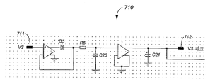
도 17은 본 발명의 실시예에 따른 출력 전압 감지 회로(710)의 개략도를 도시한다. 출력 전압 감지 회로(710)는 출력 전압을 감지하기 위해 ACF 제어기(101) 및 다른 1차측 ACF 제어기들에 통합될 수 있다. 출력 전압 감지 회로(710)는 보조 전압의 피크, 즉 보조 권선 상의 전압의 피크를 감지함으로써 출력 전압을 감지하도록 구성된다. 도 17의 예에서, 보조 전압은 ACF 제어기(101)의 VS 핀(도 17, 711; 또한 도 1, 101의 VS 핀 참조)에서 감지 전압(VS)으로서 검출된다. 출력 전압 감지 회로(710)는 노드(712)에서의 출력을 위해 감지 전압의 피크를 샘플링 및 유지한다.17 shows a schematic diagram of an output
도 18은 본 발명의 실시예에 따른 출력 전압 감지 회로(730)의 개략도를 도시한다. 출력 전압 감지 회로(730)는 출력 전압을 감지하기 위해 ACF 제어기(101) 및 다른 1차측 ACF 제어기들에 통합될 수 있다. 출력 전압 감지 회로(730)는 특정 시점에서 보조 전압의 피크를 샘플링 및 유지함으로써 출력 전압을 감지하도록 구성된다. 특정 시점은 보조 전압의 피크에 있도록 미리 설정된다. 도 18의 예에서, 보조 전압은 ACF 제어기(101)의 VS 핀(도 18, 731; 또한 도 1, 101의 VS 핀 참조)에서 감지 전압(VS)으로서 검출된다. 출력 전압 감지 회로(730)는 특정 시간에 감지 전압을 샘플링 및 유지하며, 특정 시간은 도 18의 예에서 하이측 스위치(S2)가 턴 오프된(도 18, 733) 후의 지연 시간(예컨대, 1㎲)이다. 시간 지연 회로(734)에 의해 설정되는, 지연 시간의 끝에서, 스위치(S16)는 노드(732)에서의 출력을 위해 커패시터(C14)에서 감지 전압을 샘플링 및 유지하기 위해 닫힌다.18 shows a schematic diagram of an output
도 19는 본 발명의 실시예에 따른 출력 전압 감지 회로(750)의 개략도를 도시한다. 출력 전압 감지 회로(750)는 출력 전압을 감지하기 위해 ACF 제어기(101) 및 다른 1차측 ACF 제어기들에 통합될 수 있다. 출력 전압 감지 회로(750)는, 언급된 바와 같이 nVo의 평균 및 클램프 전압의 평균과 매우 유사한, 보조 전압의 평균을 생성함으로써 출력 전압을 감지하도록 구성된다. 도 19의 예에서, 보조 전압은 ACF 제어기(101)의 VS 핀(도 19, 751; 또한 도 1, 101의 VS 핀 참조)에서 감지 전압(VS)으로서 검출된다.19 shows a schematic diagram of an output
도 19의 예에서, 출력 전압 감지 회로(750)는 피크 검출기(758) 및 최소 검출기(759)를 포함한다. 일 실시예에서, 피크 검출기(758)는 출력 전압 감지 회로(710)(도 17)와 동일한 방식으로 동작한다. 피크 검출기(758)는 감지 전압(도 19, 751)을 수신하고 노드(755)에서의 출력을 위해 감지 전압의 피크를 샘플링한다.In the example of FIG. 19, the output
일 실시예에서, 최소 검출기(759)는, 감지 전압의 최소를 샘플링한다는 점을 제외하고는, 출력 전압 감지 회로(730)(도 18)와 동일한 방식으로 동작한다. 더 구체적으로, 최소 검출기(759)는 하이측 스위치(S2)가 턴 오프된(도 19, 752) 후의 특정 시간에서 감지 전압을 샘플링 및 유지한다. 도 19의 예에서, 특정 시간은 보조 전압의 최소 값에 있도록 미리 설정된다. 특정 시간의 끝에서, 최소 검출기(759)는 감지 전압의 최소 값(도 19, 756)을 샘플링 및 유지한다. 감지 전압의 피크 및 최소 값들은 감지 전압의 평균으로서 노드(754)에서의 출력을 위해 커패시터(C51)에 유지된다.In one embodiment, the
본 발명의 실시예들은 적어도 다음을 추가로 포함한다:Embodiments of the present invention further include at least the following:
능동 클램프 플라이백 컨버터는 변압기의 1차 권선의 제1 단부에 연결된 제1 단부를 갖는 로우측 스위치 - 1차 권선의 제2 단부는 클램프 커패시터의 제1 단부에 연결됨 -; 1차 권선의 제1 단부 및 로우측 스위치의 제1 단부에 연결된 제1 단부를 갖는 하이측 스위치 - 하이측 스위치의 제2 단부는 클램프 커패시터의 제2 단부에 연결됨 -; 및 로우측 스위치의 스위칭 동작을 제어하기 위해 로우측 스위치의 제3 단부에 연결된 제1 핀, 하이측 스위치의 스위칭 동작을 제어하기 위해 하이측 스위치의 제3 단부에 연결된 제2 핀, 및 능동 클램프 플라이백 컨버터의 출력 전압을 나타내는 출력 전압 피드백 신호를 수신하는 제3 단부를 갖는 능동 클램프 플라이백(ACF) 제어기를 포함하며, ACF 제어기는 적어도 2개의 능동 클램프 스위칭 모드들로부터 선택되는 능동 클램프 스위칭 모드에 따라 하이측 스위치의 스위칭 동작을 제어하고, 능동 클램프 플라이백 컨버터의 부하의 조건에 기초하여 능동 클램프 스위칭 모드를 자동으로 선택하도록 구성되고, ACF 제어기는 지연 시간에 후속하는 데드 타임 후에 로우측 스위치를 턴 온하도록 구성되고, 지연 시간은 로우측 스위치의 드레인-소스 간 전압의 피크에서 시작된다.The active clamp flyback converter has a low side switch having a first end connected to a first end of the primary winding of the transformer, the second end of the primary winding being connected to a first end of the clamp capacitor; A high-side switch having a first end connected to the first end of the primary winding and the first end of the low-side switch, the second end of the high-side switch connected to the second end of the clamping capacitor; A first pin connected to a third end of the low side switch for controlling a switching operation of the low side switch, a second pin connected to a third end of the high side switch for controlling the switching operation of the high side switch, And an ACF controller having an ACF controller having a third end receiving an output voltage feedback signal indicative of an output voltage of the flyback converter, the ACF controller comprising an active clamp switching mode selected from at least two active clamp switching modes And the ACF controller is configured to automatically select an active clamp switching mode based on the condition of the load of the active clamp flyback converter, and after the dead time following the delay time, the low side switch And the delay time is set so that the drain-source voltage of the low-side switch It begins at large.
상기 능동 클램프 플라이백 컨버터의 다른 실시예에서, 지연 시간은 로우측 스위치의 듀티 사이클에 기초하여 적응적으로 조정된다.In another embodiment of the active clamp flyback converter, the delay time is adaptively adjusted based on the duty cycle of the low side switch.
상기 능동 클램프 플라이백 컨버터의 다른 실시예에서, 데드 타임은 로우측 스위치의 턴 온 시간 및 턴 오프 시간에 기초하여 적응적으로 조정된다.In another embodiment of the active clamp flyback converter, the dead time is adaptively adjusted based on the turn-on time and the turn-off time of the low-side switch.
능동 클램프 플라이백 컨버터는 변압기의 1차 권선의 제1 단부에 연결된 제1 단부를 갖는 로우측 스위치 - 1차 권선의 제2 단부는 클램프 커패시터의 제1 단부에 연결됨 -; 1차 권선의 제1 단부 및 로우측 스위치의 제1 단부에 연결된 제1 단부를 갖는 하이측 스위치 - 하이측 스위치의 제2 단부는 클램프 커패시터의 제2 단부에 연결됨 -; 및 로우측 스위치의 스위칭 동작을 제어하기 위해 로우측 스위치의 제3 단부에 연결된 제1 핀, 하이측 스위치의 스위칭 동작을 제어하기 위해 하이측 스위치의 제3 단부에 연결된 제2 핀, 및 능동 클램프 플라이백 컨버터의 출력 전압을 나타내는 출력 전압 피드백 신호를 수신하는 제3 단부를 갖는 능동 클램프 플라이백(ACF) 제어기를 포함하며, ACF 제어기는 적어도 2개의 능동 클램프 스위칭 모드들로부터 선택되는 능동 클램프 스위칭 모드에 따라 하이측 스위치의 스위칭 동작을 제어하고, 능동 클램프 플라이백 컨버터의 부하의 조건에 기초하여 능동 클램프 스위칭 모드를 자동으로 선택하도록 구성되고, ACF 제어기는 변압기의 보조 권선의 보조 전압으로부터 능동 클램프 플라이백 컨버터의 출력 전압을 검출하도록 구성된다.The active clamp flyback converter has a low side switch having a first end connected to a first end of the primary winding of the transformer, the second end of the primary winding being connected to a first end of the clamp capacitor; A high-side switch having a first end connected to the first end of the primary winding and the first end of the low-side switch, the second end of the high-side switch connected to the second end of the clamping capacitor; A first pin connected to a third end of the low side switch for controlling a switching operation of the low side switch, a second pin connected to a third end of the high side switch for controlling the switching operation of the high side switch, And an ACF controller having an ACF controller having a third end receiving an output voltage feedback signal indicative of an output voltage of the flyback converter, the ACF controller comprising an active clamp switching mode selected from at least two active clamp switching modes And the ACF controller is configured to automatically select the active clamp switching mode based on the conditions of the load of the active clamp flyback converter, and the ACF controller is configured to select the active clamp flyback from the auxiliary voltage of the auxiliary winding of the transformer, And to detect the output voltage of the back converter.
능동 클램프 플라이백 컨버터를 동작시키는 방법으로서, 방법은 로우측 스위치의 스위칭 동작을 제어하기 위한 로우측 게이트 구동 신호를 생성하는 단계 - 로우측 스위치의 제1 단부는 변압기의 1차 권선의 제1 단부에 연결됨 -; 하이측 스위치의 스위칭 동작을 제어하기 위한 하이측 게이트 구동 신호를 생성하는 단계 - 하이측 스위치의 제1 단부는 로우측 스위치 및 1차 권선의 제1 단부들에 연결되고, 하이측 스위치의 제2 단부는 클램프 커패시터의 제1 단부에 연결되고, 클램프 커패시터의 제2 단부는 1차 권선의 제2 단부에 연결됨 -; 능동 클램프 플라이백 컨버터의 부하를 검출하는 단계; 및 능동 클램프 플라이백 컨버터의 적어도 2개의 능동 클램프 스위칭 모드들로부터 선택되는 선택된 능동 클램프 스위칭 모드에 따라 하이측 스위치의 스위칭 동작을 제어하는 단계를 포함하고, 선택된 능동 클램프 스위칭 모드는 부하의 검출된 조건에 기초하여 선택되는, 방법.A method of operating an active clamp flyback converter, the method comprising: generating a low side gate drive signal for controlling a switching operation of a low side switch, the first end of the low side switch being connected to a first end of a primary winding of the transformer - connected to; Generating a high side gate drive signal for controlling a switching operation of the high side switch, the first end of the high side switch being connected to the first ends of the low side switch and the primary winding, The end connected to the first end of the clamp capacitor and the second end of the clamp capacitor connected to the second end of the primary winding; Detecting a load of the active clamp flyback converter; And controlling the switching operation of the high side switch in accordance with a selected active clamp switching mode selected from at least two active clamp switching modes of the active clamp flyback converter, wherein the selected active clamp switching mode is selected from the detected conditions of the load ≪ / RTI >
능동 클램프 플라이백 컨버터를 동작시키는 상기 방법의 다른 실시예에서, 선택된 능동 클램프 스위칭 모드는 상보적인 능동 클램프 모드이고, 방법은 상보적인 능동 클램프 모드 동안에 부하가 증가함에 따라 로우측 스위치의 스위칭 주파수를 감소시키는 단계를 더 포함한다.In another embodiment of the above method of operating the active clamp flyback converter, the selected active clamp switching mode is a complementary active clamp mode and the method reduces the switching frequency of the low side switch as the load increases during the complementary active clamp mode .
능동 클램프 플라이백 컨버터를 동작시키는 상기 방법의 다른 실시예에서, 선택된 능동 클램프 스위칭 모드는 수정된 능동 클램프 모드이고, 방법은 의사 공진 스위칭(QRS) 블랭킹 시간의 만료 후에 QRS에 따라 하이측 스위치를 턴 온하는 단계; 및 수정된 능동 클램프 모드에서 부하가 감소함에 따라 QRS 블랭킹 시간을 증가시키는 단계를 더 포함한다.In another embodiment of the above method of operating the active clamp flyback converter, the selected active clamp switching mode is a modified active clamp mode, and the method turns the high side switch according to QRS after the expiration of the quasi-resonance switching (QRS) blanking time Turning on; And increasing the QRS blanking time as the load decreases in the modified active clamp mode.
능동 클램프 플라이백 컨버터를 동작시키는 상기 방법의 다른 실시예에서, 선택된 능동 클램프 스위칭 모드는 수정된 능동 클램프 모드이고, 수정된 능동 클램프 모드에서, 방법은 능동 클램프 플라이백 컨버터의 스위칭 사이클에서 로우측 스위치가 턴 오프된 후에 하이측 스위치를 턴 온하기 위해 하이측 게이트 구동 신호의 제1 펄스를 생성하는 단계; 및 능동 클램프 플라이백 컨버터의 동일한 스위칭 사이클에서 하이측 스위치를 턴 온하기 위해 하이측 게이트 구동 신호의 제2 펄스를 생성하는 단계를 더 포함한다.In another embodiment of the above method of operating the active clamp flyback converter, the selected active clamp switching mode is a modified active clamp mode, and in a modified active clamp mode, the method includes switching the low side switch Generating a first pulse of the high side gate drive signal to turn on the high side switch after turning off the high side gate drive signal; And generating a second pulse of the high side gate drive signal to turn on the high side switch in the same switching cycle of the active clamp flyback converter.
능동 클램프 플라이백 컨버터를 동작시키는 상기 방법의 다른 실시예에서, 하이측 게이트 구동 신호의 제1 펄스는 제로 전압 스위칭(ZVS)에 따라 생성되고, 하이측 게이트 구동 신호의 제2 펄스는 의사 공진 스위칭(QRS) 블랭킹 시간의 만료 후에 QRS에 따라 생성된다.In another embodiment of the above method of operating the active clamp flyback converter, a first pulse of the high side gate drive signal is generated according to a zero voltage switch (ZVS) and a second pulse of the high side gate drive signal is generated by a quasi-resonant switching (QRS) is generated according to the QRS after the expiration of the blanking time.
능동 클램프 플라이백 컨버터를 동작시키는 상기 방법의 다른 실시예에서, 능동 클램프 플라이백 컨버터의 부하를 검출하는 단계는 로우측 스위치의 드레인 전류를 적분하여 적분된 신호를 생성하는 단계; 및 적분된 신호, 능동 클램프 플라이백 컨버터의 입력 전압, 및 로우측 스위치의 스위칭 주파수에 기초하여 플라이백 컨버터의 출력 전력을 결정하는 단계를 포함한다.In another embodiment of the method for operating an active clamp flyback converter, detecting the load of the active clamp flyback converter comprises integrating the drain current of the low side switch to produce an integrated signal; And determining the output power of the flyback converter based on the integrated signal, the input voltage of the active clamp flyback converter, and the switching frequency of the low side switch.
능동 클램프 플라이백 컨버터를 동작시키는 상기 방법의 다른 실시예에서, 방법은 변압기의 보조 권선의 보조 전압으로부터 능동 클램프 플라이백 컨버터의 출력 전압을 검출하는 단계를 더 포함한다.In another embodiment of the above method of operating the active clamp flyback converter, the method further comprises detecting an output voltage of the active clamp flyback converter from an auxiliary voltage of the auxiliary winding of the transformer.
능동 클램프 플라이백 컨버터를 위한 능동 클램프 플라이백(ACF) 제어기로서, 로우측 스위치의 게이트에 연결된 제1 핀; 하이측 스위치의 게이트에 연결된 제2 핀; 로우측 스위치의 스위칭 동작을 제어하기 위한 로우측 게이트 구동 신호를 생성하고, 하이측 스위치의 스위칭 동작을 제어하기 위한 하이측 게이트 구동 신호를 생성하고, 제1 능동 클램프 스위칭 모드 동안 능동 클램프 플라이백 컨버터의 부하가 증가함에 따라 로우측 스위치의 스위칭 주파수를 감소시키고, 제2 능동 클램프 스위칭 모드 동안 부하가 감소함에 따라 하이측 스위치의 의사 공진 스위칭(QRS) 블랭킹 시간을 증가시키고, 부하의 조건에 기초하여 제1 능동 클램프 스위칭 모드와 제2 능동 클램프 스위칭 모드 사이에서 스위칭하는 발진기를 포함하는, ACF 제어기.An active clamp flyback (ACF) controller for an active clamp flyback converter, comprising: a first pin coupled to a gate of a low side switch; A second pin connected to the gate of the high side switch; Side switch to generate a low-side gate drive signal for controlling the switching operation of the low-side switch, to generate a high-side gate drive signal for controlling the switching operation of the high-side switch, and to provide an active clamp flyback converter Resonant switching (QRS) blanking time of the high side switch as the load decreases during the second active clamp switching mode, and based on the condition of the load And an oscillator that switches between a first active clamp switching mode and a second active clamp switching mode.
상기 ACF 제어기의 다른 실시예에서, 발진기는 제로 전압 스위칭(ZVS)에 따라 하이측 게이트 구동 신호의 제1 펄스를 생성하고 QRS에 따라 하이측 게이트 구동 신호의 제2 펄스를 생성한다.In another embodiment of the ACF controller, the oscillator generates a first pulse of the high side gate drive signal in accordance with zero voltage switching (ZVS) and generates a second pulse of the high side gate drive signal in accordance with QRS.
상기 ACF 제어기의 다른 실시예에서, 로우측 스위치의 드레인은 변압기의 1차 권선의 제1 단부에 연결되고, 로우측 스위치의 소스는 접지에 연결되고, 하이측 스위치의 소스는 로우측 스위치의 드레인에 연결되고, 하이측 스위치의 드레인은 클램프 커패시터의 제1 단부에 연결되고, 클램프 커패시터의 제2 단부는 1차 권선의 제2 단부에 연결된다.In another embodiment of the ACF controller, the drain of the low side switch is connected to the first end of the primary winding of the transformer, the source of the low side switch is connected to ground and the source of the high side switch is the drain of the low side switch The drain of the high side switch is connected to the first end of the clamp capacitor and the second end of the clamp capacitor is connected to the second end of the primary winding.
능동 클램프 플라이백 컨버터에 대한 회로들 및 방법들이 개시되었다.Circuits and methods for an active clamp flyback converter have been disclosed.
본 발명의 특정 실시예들이 제공되었지만, 이들 실시예는 예시 목적을 위한 것이며 제한적인 것이 아니라는 것을 이해해야 한다. 본 개시를 읽는 당업자에게 많은 추가적인 실시예들이 명백할 것이다.While specific embodiments of the invention have been provided, it is to be understood that these embodiments are for the purpose of illustration and not of limitation. Many additional embodiments will be apparent to those skilled in the art upon reading this disclosure.
Claims (6)
변압기의 1차 권선의 제1 단부에 연결된 제1 단부를 갖는 로우측 스위치(low-side switch) - 상기 1차 권선의 제2 단부는 클램프 커패시터의 제1 단부에 연결됨 -;
상기 1차 권선의 상기 제1 단부 및 상기 로우측 스위치의 상기 제1 단부에 연결된 제1 단부를 갖는 하이측 스위치(high-side switch) - 상기 하이측 스위치의 제2 단부는 상기 클램프 커패시터의 제2 단부에 연결됨 -; 및
상기 로우측 스위치의 스위칭 동작을 제어하기 위해 상기 로우측 스위치의 제3 단부에 연결된 제1 핀, 상기 하이측 스위치의 스위칭 동작을 제어하기 위해 상기 하이측 스위치의 제3 단부에 연결된 제2 핀, 및 상기 능동 클램프 플라이백 컨버터의 출력 전압을 나타내는 출력 전압 피드백 신호를 수신하는 제3 단부를 갖는 능동 클램프 플라이백(ACF) 제어기 - 상기 ACF 제어기는 적어도 2개의 능동 클램프 스위칭 모드들로부터 선택되는 능동 클램프 스위칭 모드에 따라 상기 하이측 스위치의 상기 스위칭 동작을 제어하고, 상기 능동 클램프 플라이백 컨버터의 부하의 조건에 기초하여 상기 능동 클램프 스위칭 모드를 자동으로 선택하도록 구성됨 -
를 포함하는, 능동 클램프 플라이백 컨버터.As an active clamp flyback converter,
A low-side switch having a first end connected to a first end of the primary winding of the transformer, the second end of the primary winding connected to a first end of the clamp capacitor;
A high-side switch having a first end connected to the first end of the primary winding and a first end connected to the first end of the low-side switch, the second end of the high- Connected to two ends; And
A first pin connected to a third end of the low side switch for controlling a switching operation of the low side switch, a second pin connected to a third end of the high side switch for controlling a switching operation of the high side switch, And an ACF controller having an active clamp flyback (ACF) controller having a third end receiving an output voltage feedback signal indicative of an output voltage of the active clamp flyback converter, the ACF controller comprising an active clamp selected from at least two active clamp switching modes Wherein the controller is configured to control the switching operation of the high side switch according to a switching mode and to automatically select the active clamp switching mode based on a condition of a load of the active clamp flyback converter,
And an active clamp flyback converter.
상기 ACF 제어기는 상기 로우측 스위치의 상기 스위칭 동작을 제어하기 위해 상기 제1 핀에서 로우측 게이트 구동 신호를 생성하고, 상기 하이측 스위치의 상기 스위칭 동작을 제어하기 위해 상기 제2 핀에서 하이측 게이트 구동 신호를 생성하고, 상기 상보적인 능동 클램프 모드 동안 상기 부하가 증가함에 따라 상기 로우측 스위치의 스위칭 주파수를 감소시키도록 구성되는, 능동 클램프 플라이백 컨버터.The method of claim 1, wherein the active clamp switching mode is a complementary active clamp mode,
The ACF controller generates a low side gate drive signal at the first pin to control the switching operation of the low side switch and controls the high side gate at the second pin to control the switching operation of the high side switch, And to reduce the switching frequency of the low side switch as the load increases during the complementary active clamp mode.
상기 ACF 제어기는 상기 로우측 스위치의 상기 스위칭 동작을 제어하기 위해 상기 제1 핀에서 로우측 게이트 구동 신호를 생성하고, 상기 하이측 스위치의 상기 스위칭 동작을 제어하기 위해 상기 제2 핀에서 하이측 게이트 구동 신호를 생성하고, 상기 능동 클램프 플라이백 컨버터의 스위칭 사이클에서 상기 로우측 스위치가 턴 오프된 후에 상기 하이측 스위치를 턴 온하기 위해 상기 하이측 게이트 구동 신호의 제1 펄스를 생성하고, 상기 수정된 능동 클램프 모드에서 상기 능동 클램프 플라이백 컨버터의 동일한 스위칭 사이클에서 상기 하이측 스위치를 턴 온하기 위해 상기 하이측 게이트 구동 신호의 제2 펄스를 생성하도록 구성되는, 능동 클램프 플라이백 컨버터.2. The method of claim 1, wherein the active clamp switching mode is a modified active clamp mode,
The ACF controller generates a low side gate drive signal at the first pin to control the switching operation of the low side switch and controls the high side gate at the second pin to control the switching operation of the high side switch, Generating a drive signal and generating a first pulse of the high side gate drive signal to turn on the high side switch after the low side switch is turned off in a switching cycle of the active clamp flyback converter, Side gate drive signal to turn on the high side switch in the same switching cycle of the active clamp flyback converter in an active clamp mode.
Applications Claiming Priority (6)
| Application Number | Priority Date | Filing Date | Title |
|---|---|---|---|
| US201662307431P | 2016-03-12 | 2016-03-12 | |
| US62/307,431 | 2016-03-12 | ||
| US201662334104P | 2016-05-10 | 2016-05-10 | |
| US62/334,104 | 2016-05-10 | ||
| US15/418,887 | 2017-01-30 | ||
| US15/418,887 US10069426B2 (en) | 2016-03-12 | 2017-01-30 | Active clamp flyback converter |
Publications (1)
| Publication Number | Publication Date |
|---|---|
| KR20170106204A true KR20170106204A (en) | 2017-09-20 |
Family
ID=59787252
Family Applications (1)
| Application Number | Title | Priority Date | Filing Date |
|---|---|---|---|
| KR1020170028064A Abandoned KR20170106204A (en) | 2016-03-12 | 2017-03-06 | Active clamp flyback converter |
Country Status (3)
| Country | Link |
|---|---|
| US (1) | US10069426B2 (en) |
| KR (1) | KR20170106204A (en) |
| CN (2) | CN107181410B (en) |
Cited By (5)
| Publication number | Priority date | Publication date | Assignee | Title |
|---|---|---|---|---|
| WO2019123247A1 (en) * | 2017-12-21 | 2019-06-27 | Silanna Asia Pte Ltd | Power converter with active clamp |
| US10461626B1 (en) | 2019-01-14 | 2019-10-29 | Silanna Asia Pte Ltd | Active clamp circuit |
| US10707766B2 (en) | 2018-02-02 | 2020-07-07 | Silanna Asia Pte Ltd | Integrated self-driven active clamp |
| KR20220115519A (en) * | 2021-02-10 | 2022-08-17 | 후아웨이 디지털 파워 테크놀러지스 컴퍼니 리미티드 | Converter and power adapter |
| KR20230139857A (en) * | 2022-03-23 | 2023-10-06 | 중앙대학교 산학협력단 | Control device and control method to reduce the output voltage deviation of active clamp converter |
Families Citing this family (67)
| Publication number | Priority date | Publication date | Assignee | Title |
|---|---|---|---|---|
| EP3024133A1 (en) * | 2014-11-24 | 2016-05-25 | Broadband Power Solutions | DC-to-AC power converter |
| US9716437B2 (en) * | 2015-12-18 | 2017-07-25 | Champion Microelectronic Corporation | Power converter for a switching power supply and manner of operation thereof |
| TWI624144B (en) * | 2016-09-19 | 2018-05-11 | 國立成功大學 | Flyback converter and controlling method thereof |
| US9991803B1 (en) * | 2017-01-18 | 2018-06-05 | Semiconductor Components Industries, Llc | Reduction of electromagnetic interference in a flyback converter |
| US9935556B1 (en) * | 2017-01-27 | 2018-04-03 | Semiconductor Components Industries, Llc | Primary-side control of resonant converters |
| US20190036459A1 (en) * | 2017-04-28 | 2019-01-31 | Astec International Limited | Flyback power converters including adaptive clamp circuits for adjusting resonant frequencies |
| US10312817B2 (en) * | 2017-07-07 | 2019-06-04 | Semiconductor Components Industries, Llc | Systems and methods of active clamp flyback power converters |
| TWI652890B (en) * | 2017-07-27 | 2019-03-01 | 群光電能科技股份有限公司 | Power conversion system with clamp mode switching |
| JP6937638B2 (en) * | 2017-08-25 | 2021-09-22 | ローム株式会社 | DC / DC converters and their control circuits, control methods, and electronic devices |
| US10320301B2 (en) | 2017-09-15 | 2019-06-11 | Semiconductor Components Industries, Llc | Power converter responsive to device connection status |
| TWI650926B (en) * | 2017-10-16 | 2019-02-11 | 立錡科技股份有限公司 | Return-type power conversion circuit with active clamp and conversion control circuit and control method thereof |
| CN109713904B (en) * | 2017-10-26 | 2020-11-24 | 立锜科技股份有限公司 | Flyback power conversion circuit and conversion control circuit and control method therein |
| US10141830B1 (en) * | 2017-10-31 | 2018-11-27 | Semiconductor Components Industries, Llc | Burst operation of a switching controller having a plurality of foldback curves |
| US10530260B2 (en) * | 2018-01-19 | 2020-01-07 | Dialog Semiconductor Inc. | Adaptive control for zero-voltage switching in a multi-switch switching power converter |
| EP3764529B1 (en) * | 2018-03-07 | 2022-09-21 | Nissan Motor Co., Ltd. | Method for controlling resonant power conversion device, resonant power conversion device, and dc-dc converter |
| CN110247554B (en) * | 2018-03-09 | 2020-09-11 | 台达电子工业股份有限公司 | Transformer and its control method |
| US10438900B1 (en) | 2018-03-29 | 2019-10-08 | Alpha And Omega Semiconductor (Cayman) Ltd. | HV converter with reduced EMI |
| CN108738223B (en) * | 2018-06-18 | 2020-11-06 | 安徽航天环境工程有限公司 | Plasma treatment device for gaseous waste |
| CN108811291A (en) * | 2018-06-18 | 2018-11-13 | 安徽航天环境工程有限公司 | A kind of low-temperature plasma device |
| CN108771954A (en) * | 2018-06-18 | 2018-11-09 | 安徽航天环境工程有限公司 | A kind of includes the plasma treatment appts of nitrogen oxides and oxysulfide |
| EP3591826B1 (en) * | 2018-07-03 | 2021-02-24 | Delta Electronics (Shanghai) Co., Ltd. | Method and apparatus for controlling a flyback converter |
| US11349397B2 (en) * | 2018-07-03 | 2022-05-31 | Delta Electronics (Shanghai) Co., Ltd. | Method and apparatus for controlling a flyback converter |
| JP6853851B2 (en) * | 2018-07-03 | 2021-03-31 | 台達電子企業管理(上海)有限公司 | Flyback converter control method and equipment |
| CN108988647A (en) * | 2018-07-04 | 2018-12-11 | 广州金升阳科技有限公司 | A kind of switch converters |
| CN108809107B (en) * | 2018-07-13 | 2019-08-23 | 深圳南云微电子有限公司 | A kind of method and circuit of the self adaptive control of active clamp flyback converter |
| CN109245569B (en) * | 2018-09-18 | 2020-04-24 | 西安矽力杰半导体技术有限公司 | Flyback converter and control circuit thereof |
| TWI687034B (en) * | 2018-09-18 | 2020-03-01 | 通嘉科技股份有限公司 | Active clamp flyback converter capable of switching operation modes |
| CN110957915B (en) * | 2018-09-27 | 2021-09-07 | 通嘉科技股份有限公司 | Active-clamp flyback power converter with switchable operating modes |
| TWI672896B (en) * | 2018-09-28 | 2019-09-21 | 通嘉科技股份有限公司 | Active clamp flyback converters and control methods thereof |
| CN111030479B (en) * | 2018-10-09 | 2022-09-27 | 通嘉科技股份有限公司 | Active-clamp flyback power converter and associated control method |
| CN109639149B (en) | 2018-12-26 | 2020-07-28 | 西安华为技术有限公司 | ACF converter, voltage conversion method and electronic equipment |
| CN111585440B (en) * | 2019-02-18 | 2022-06-17 | 东南大学 | Control system and method of active clamp flyback converter |
| CN111585441B (en) * | 2019-02-18 | 2022-06-17 | 东南大学 | Control system and method for primary side regulation active clamping flyback converter |
| CN109713907B (en) * | 2019-03-05 | 2020-06-19 | 深圳南云微电子有限公司 | Control method and circuit of switching power supply |
| EP3959807B1 (en) * | 2019-04-24 | 2023-06-07 | Power Integrations, Inc. | Power converter comprising an active non-dissipative clamp circuit, and respective controller. |
| US11632054B2 (en) | 2019-04-24 | 2023-04-18 | Power Integrations, Inc. | Mode operation detection for control of a power converter with an active clamp switch |
| CN112117905B (en) * | 2019-06-20 | 2021-12-21 | 东南大学 | Control system and method of active clamp flyback converter |
| US11509227B2 (en) * | 2019-07-19 | 2022-11-22 | Texas Instruments Incorporated | Active clamp flyback converter |
| CN110677045B (en) * | 2019-09-20 | 2020-09-15 | 广州金升阳科技有限公司 | Control method of active clamp flyback converter |
| TWI708462B (en) * | 2019-09-25 | 2020-10-21 | 偉詮電子股份有限公司 | Control method in use of active-clamp flyback power converter |
| US10904975B1 (en) * | 2019-10-09 | 2021-01-26 | Infineon Technologies Austria Ag | Dimming for open-loop resonate converters |
| US10965218B1 (en) | 2019-11-15 | 2021-03-30 | Power Integrations, Inc. | Active clamp circuit with steering network |
| TWI729585B (en) * | 2019-11-22 | 2021-06-01 | 亞源科技股份有限公司 | Dual mode active clamp flyback converter |
| CN110912414B (en) * | 2019-12-11 | 2023-02-28 | 亚瑞源科技(深圳)有限公司 | Dual-mode active-clamping flyback converter |
| US10985665B1 (en) * | 2020-01-03 | 2021-04-20 | Huayuan Semiconductor (Shenzhen) Limited Company | Voltage sensing of an active clamp switching power converter circuit using an auxiliary winding having a same polarity as a primary winding |
| US11239740B2 (en) | 2020-03-18 | 2022-02-01 | Huayuan Semiconductor (Shenzhen) Limited Company | Voltage sensing of an active clamp switching power converter circuit using auxiliary winding having an opposite polarity as a primary winding |
| US11050350B1 (en) * | 2020-03-20 | 2021-06-29 | Huayuan Semiconductor (Shenzhen) Limited Company | Controlling an active clamp switching power converter circuit based on a sensed voltage drop on an auxiliary winding |
| CN114844185B (en) | 2020-04-10 | 2024-09-24 | 华为数字能源技术有限公司 | A charging device and control method thereof, and a charging system |
| CN111628630A (en) * | 2020-05-09 | 2020-09-04 | 华南师范大学 | Flyback conversion circuit and switching power supply circuit |
| TWI732581B (en) * | 2020-06-03 | 2021-07-01 | 亞源科技股份有限公司 | Conversion device with oscillation reduction control and method of operation of oscillation reduction control the same |
| CN114070074B (en) * | 2020-07-30 | 2022-12-30 | 华为数字能源技术有限公司 | Double-tube flyback conversion circuit, power module, electric automobile and control method |
| WO2022027658A1 (en) * | 2020-08-07 | 2022-02-10 | 华为数字能源技术有限公司 | Active clamp flyback circuit |
| CN111953186B (en) * | 2020-08-12 | 2024-03-29 | 东科半导体(安徽)股份有限公司 | Switching power supply control circuit |
| CN114568042B (en) * | 2020-09-30 | 2023-04-18 | 英诺赛科(苏州)科技有限公司 | Flyback converter and operation method thereof |
| CN112532066A (en) * | 2020-11-16 | 2021-03-19 | 上海百功半导体有限公司 | Novel zero-voltage switching control circuit and method and voltage converter |
| WO2022147683A1 (en) * | 2021-01-06 | 2022-07-14 | Astec International Limited | High side active clamp charging circuit |
| CN112928923B (en) * | 2021-02-01 | 2022-05-03 | 杭州电子科技大学 | Asymmetric half-bridge flyback converter and implementation method thereof |
| CN113937988B (en) * | 2021-06-28 | 2024-03-22 | 杰华特微电子股份有限公司 | Asymmetric half-bridge flyback converter and control method thereof |
| US12136883B2 (en) * | 2021-09-30 | 2024-11-05 | Stmicroelectronics S.R.L. | Method for operating in burst mode active clamp flyback converters and corresponding active clamp flyback converter apparatus |
| CN114710012B (en) * | 2021-11-04 | 2025-12-09 | 杰华特微电子股份有限公司 | Control method and control circuit of switching power supply and switching power supply |
| CN114189160B (en) * | 2021-12-07 | 2023-12-12 | 南京微盟电子有限公司 | Light-load conduction control method and circuit for clamping tube in active clamping flyback topology |
| CN118174555A (en) * | 2022-12-09 | 2024-06-11 | 台达电子企业管理(上海)有限公司 | Switching power converter and control method thereof |
| US20240322693A1 (en) * | 2023-03-24 | 2024-09-26 | Silanna Asia Pte Ltd | Flyback Converter Active Clamp Control System and Methods |
| JP2025010878A (en) * | 2023-07-10 | 2025-01-23 | サンケン電気株式会社 | Active clamp flyback converter and control IC |
| US20250149991A1 (en) * | 2023-11-02 | 2025-05-08 | Stmicroelectronics International N.V. | Automatic reverse current adjustment in an active clamp flyback converter |
| US20250373167A1 (en) * | 2024-05-31 | 2025-12-04 | Stmicroelectronics International N.V. | Active clamp flyback short circuit protection |
| CN120090442B (en) * | 2025-04-30 | 2025-08-01 | 无锡硅动力微电子股份有限公司 | A dual-phase configuration clamp drive circuit for a forward active clamp PWM controller |
Family Cites Families (24)
| Publication number | Priority date | Publication date | Assignee | Title |
|---|---|---|---|---|
| JP3580297B2 (en) * | 2002-04-01 | 2004-10-20 | 日産自動車株式会社 | Semiconductor device with current detection function |
| GB0523087D0 (en) * | 2005-11-11 | 2005-12-21 | Alstom Power Conversion Ltd | Power converters |
| US7778051B2 (en) * | 2007-03-14 | 2010-08-17 | System General Corp. | Output current control circuit for power converter with a changeable switching frequency |
| US20080316779A1 (en) * | 2007-06-19 | 2008-12-25 | Chandrasekaran Jayaraman | System and method for estimating input power for a power processing circuit |
| US7619909B2 (en) * | 2007-12-07 | 2009-11-17 | Leadtrend Technology Corp. | Control circuit for adjusting leading edge blanking time and power converting system using the same control circuit |
| EP2300695A1 (en) * | 2008-04-17 | 2011-03-30 | Andrew C. Berkun | Energy conversion devices and systems including the same |
| TWI358188B (en) * | 2008-09-17 | 2012-02-11 | Delta Electronics Inc | Forward-flyback converter with active-clamp circui |
| JP5170117B2 (en) * | 2010-01-18 | 2013-03-27 | 株式会社村田製作所 | Switching control circuit and switching power supply device |
| CN102684507A (en) * | 2011-03-17 | 2012-09-19 | 国琏电子(上海)有限公司 | Flyback switching power supply |
| CN102185484B (en) * | 2011-05-10 | 2013-09-18 | 成都芯源系统有限公司 | Switching power supply and control circuit and control method thereof |
| CN102185466B (en) * | 2011-05-24 | 2013-03-27 | 矽力杰半导体技术(杭州)有限公司 | Driving circuit and driving method applied to flyback-type converter and quasi-resonant soft-switching flyback-type converter applying same |
| CN102684460B (en) * | 2012-05-24 | 2014-07-16 | 佛山市南海赛威科技技术有限公司 | Frequency soft clamp system for quasi-resonant switching power supply and method |
| US9882497B2 (en) * | 2012-09-28 | 2018-01-30 | Microchip Technology Incorporated | Soft switching synchronous quasi resonant converter |
| US8929101B2 (en) * | 2012-12-17 | 2015-01-06 | Chung-Shan Institute Of Science And Technology | DC to DC converting circuit |
| US9391528B2 (en) * | 2012-12-27 | 2016-07-12 | Fairchild (Taiwan) Corporation | Active clamp circuits for flyback power converters |
| TWI525975B (en) * | 2013-02-18 | 2016-03-11 | 崇貿科技股份有限公司 | Control circuit of flyback power converter |
| US9136765B2 (en) * | 2013-03-08 | 2015-09-15 | Power Integrations, Inc. | Techniques for controlling a power converter using multiple controllers |
| US10205397B2 (en) * | 2014-07-10 | 2019-02-12 | Rompower Technology Holdings, Llc | Soft switching on all switching elements converter through current shaping “bucharest converter” |
| US9276483B2 (en) * | 2013-06-27 | 2016-03-01 | System General Corporation | Control circuit for active-clamp flyback power converter with programmable switching period |
| US9077254B2 (en) * | 2013-07-12 | 2015-07-07 | Solantro Semiconductor Corp. | Switching mode power supply using pulse mode active clamping |
| US9543821B2 (en) * | 2014-06-10 | 2017-01-10 | Power Integrations, Inc. | MOSFET driver with pulse timing pattern fault detection and adaptive safe operating area mode of operation |
| CN104601027A (en) * | 2015-01-12 | 2015-05-06 | 南京亚派科技股份有限公司 | Tandem double flyback quasi resonant converter suitable for neutral point clamped direct current bus |
| CN204517693U (en) * | 2015-01-12 | 2015-07-29 | 南京亚派科技股份有限公司 | A kind of two flyback quasi resonant convertor of series connection being applicable to neutral-point-clamped DC bus |
| US9716437B2 (en) * | 2015-12-18 | 2017-07-25 | Champion Microelectronic Corporation | Power converter for a switching power supply and manner of operation thereof |
-
2017
- 2017-01-30 US US15/418,887 patent/US10069426B2/en active Active
- 2017-03-06 KR KR1020170028064A patent/KR20170106204A/en not_active Abandoned
- 2017-03-10 CN CN201710139716.3A patent/CN107181410B/en active Active
- 2017-03-10 CN CN202011255748.8A patent/CN112271929B/en active Active
Cited By (13)
| Publication number | Priority date | Publication date | Assignee | Title |
|---|---|---|---|---|
| US10811986B2 (en) | 2017-12-21 | 2020-10-20 | Appulse Power Inc. | Power converter with active clamp |
| US10418912B2 (en) | 2017-12-21 | 2019-09-17 | Silanna Asia Pte Ltd | Power converter with active clamp |
| US11316436B2 (en) | 2017-12-21 | 2022-04-26 | Appulse Power Inc. | Active clamp controller circuit |
| WO2019123247A1 (en) * | 2017-12-21 | 2019-06-27 | Silanna Asia Pte Ltd | Power converter with active clamp |
| US11095228B2 (en) | 2018-02-02 | 2021-08-17 | Appulse Power Inc. | Integrated self-driven active clamp |
| US10707766B2 (en) | 2018-02-02 | 2020-07-07 | Silanna Asia Pte Ltd | Integrated self-driven active clamp |
| US11671026B2 (en) | 2018-02-02 | 2023-06-06 | Appulse Power Inc. | Integrated self-driven active clamp |
| US11038412B2 (en) | 2019-01-14 | 2021-06-15 | Appulse Power Inc. | Active clamp circuit |
| US10461626B1 (en) | 2019-01-14 | 2019-10-29 | Silanna Asia Pte Ltd | Active clamp circuit |
| US11456657B2 (en) | 2019-01-14 | 2022-09-27 | Appulse Power Inc. | Active clamp circuit |
| KR20220115519A (en) * | 2021-02-10 | 2022-08-17 | 후아웨이 디지털 파워 테크놀러지스 컴퍼니 리미티드 | Converter and power adapter |
| US11843318B2 (en) | 2021-02-10 | 2023-12-12 | Huawei Digital Power Technologies Co., Ltd. | Converter and power adapter for reducing energy loss |
| KR20230139857A (en) * | 2022-03-23 | 2023-10-06 | 중앙대학교 산학협력단 | Control device and control method to reduce the output voltage deviation of active clamp converter |
Also Published As
| Publication number | Publication date |
|---|---|
| CN107181410B (en) | 2020-12-08 |
| CN107181410A (en) | 2017-09-19 |
| CN112271929B (en) | 2024-05-28 |
| US20170264206A1 (en) | 2017-09-14 |
| CN112271929A (en) | 2021-01-26 |
| US10069426B2 (en) | 2018-09-04 |
Similar Documents
| Publication | Publication Date | Title |
|---|---|---|
| CN112271929B (en) | Active Clamp Flyback Converter | |
| US10879791B2 (en) | DC/DC resonant converters and power factor correction using resonant converters, and corresponding control methods | |
| US8054655B2 (en) | Tail current control of isolated converter and apparatus thereof | |
| US9948187B2 (en) | System and method for a switched-mode power supply | |
| EP3414824B1 (en) | Dc/dc resonant converters and power factor correction using resonant converters, and corresponding control methods | |
| US9647562B2 (en) | Power conversion with switch turn-off delay time compensation | |
| US10686387B2 (en) | Multi-transformer LLC resonant converter circuit | |
| TW201018062A (en) | Control circuit having off-time modulation to operate power converter at quasi-resonance and in continuous current mode | |
| US10418913B2 (en) | DC/DC resonant converters and power factor correction using resonant converters, and corresponding control methods | |
| US9935547B2 (en) | System and method for a switched-mode power supply | |
| JP2016174471A (en) | Snubber circuit | |
| US9001538B2 (en) | Switching power supply apparatus | |
| US10355610B2 (en) | LLC power converter and switching method thereof | |
| KR101141374B1 (en) | Boost converter | |
| KR20150044317A (en) | Converter and driving method thereof | |
| EP1513248A2 (en) | Switching electric source device | |
| US10734889B2 (en) | DC/DC resonant converters and power factor correction using resonant converters, and corresponding control methods | |
| US10447147B2 (en) | DC/DC resonant converters and power factor correction using resonant converters, and corresponding control methods | |
| US11699956B2 (en) | Cycle-by-cycle reverse current limiting in ACF converters | |
| WO2024201170A1 (en) | Flyback converter active clamp control system and methods | |
| Ghanbari et al. | Proposing a multimode switching control method for a half-bridge converter to improve its efficiency over the entire load variations | |
| EP4503412A1 (en) | Power converter with a sensing circuit and method | |
| TWI677177B (en) | Power supply control unit and isolation type switching power supply device |
Legal Events
| Date | Code | Title | Description |
|---|---|---|---|
| PA0109 | Patent application |
Patent event code: PA01091R01D Comment text: Patent Application Patent event date: 20170306 |
|
| PG1501 | Laying open of application | ||
| A201 | Request for examination | ||
| PA0201 | Request for examination |
Patent event code: PA02012R01D Patent event date: 20190215 Comment text: Request for Examination of Application Patent event code: PA02011R01I Patent event date: 20170306 Comment text: Patent Application |
|
| E902 | Notification of reason for refusal | ||
| PE0902 | Notice of grounds for rejection |
Comment text: Notification of reason for refusal Patent event date: 20200801 Patent event code: PE09021S01D |
|
| E701 | Decision to grant or registration of patent right | ||
| PE0701 | Decision of registration |
Patent event code: PE07011S01D Comment text: Decision to Grant Registration Patent event date: 20210203 |
|
| NORF | Unpaid initial registration fee | ||
| PC1904 | Unpaid initial registration fee |