EP3764529B1 - Method for controlling resonant power conversion device, resonant power conversion device, and dc-dc converter - Google Patents
Method for controlling resonant power conversion device, resonant power conversion device, and dc-dc converter Download PDFInfo
- Publication number
- EP3764529B1 EP3764529B1 EP18909189.5A EP18909189A EP3764529B1 EP 3764529 B1 EP3764529 B1 EP 3764529B1 EP 18909189 A EP18909189 A EP 18909189A EP 3764529 B1 EP3764529 B1 EP 3764529B1
- Authority
- EP
- European Patent Office
- Prior art keywords
- switching element
- frequency
- switching
- voltage
- delay time
- Prior art date
- Legal status (The legal status is an assumption and is not a legal conclusion. Google has not performed a legal analysis and makes no representation as to the accuracy of the status listed.)
- Active
Links
Images


Classifications
-
- H—ELECTRICITY
- H02—GENERATION; CONVERSION OR DISTRIBUTION OF ELECTRIC POWER
- H02M—APPARATUS FOR CONVERSION BETWEEN AC AND AC, BETWEEN AC AND DC, OR BETWEEN DC AND DC, AND FOR USE WITH MAINS OR SIMILAR POWER SUPPLY SYSTEMS; CONVERSION OF DC OR AC INPUT POWER INTO SURGE OUTPUT POWER; CONTROL OR REGULATION THEREOF
- H02M3/00—Conversion of DC power input into DC power output
- H02M3/02—Conversion of DC power input into DC power output without intermediate conversion into AC
- H02M3/04—Conversion of DC power input into DC power output without intermediate conversion into AC by static converters
- H02M3/10—Conversion of DC power input into DC power output without intermediate conversion into AC by static converters using discharge tubes with control electrode or semiconductor devices with control electrode
- H02M3/145—Conversion of DC power input into DC power output without intermediate conversion into AC by static converters using discharge tubes with control electrode or semiconductor devices with control electrode using devices of a triode or transistor type requiring continuous application of a control signal
- H02M3/155—Conversion of DC power input into DC power output without intermediate conversion into AC by static converters using discharge tubes with control electrode or semiconductor devices with control electrode using devices of a triode or transistor type requiring continuous application of a control signal using semiconductor devices only
- H02M3/156—Conversion of DC power input into DC power output without intermediate conversion into AC by static converters using discharge tubes with control electrode or semiconductor devices with control electrode using devices of a triode or transistor type requiring continuous application of a control signal using semiconductor devices only with automatic control of output voltage or current, e.g. switching regulators
-
- H—ELECTRICITY
- H02—GENERATION; CONVERSION OR DISTRIBUTION OF ELECTRIC POWER
- H02M—APPARATUS FOR CONVERSION BETWEEN AC AND AC, BETWEEN AC AND DC, OR BETWEEN DC AND DC, AND FOR USE WITH MAINS OR SIMILAR POWER SUPPLY SYSTEMS; CONVERSION OF DC OR AC INPUT POWER INTO SURGE OUTPUT POWER; CONTROL OR REGULATION THEREOF
- H02M1/00—Details of apparatus for conversion
- H02M1/08—Circuits specially adapted for the generation of control voltages for semiconductor devices incorporated in static converters
- H02M1/083—Circuits specially adapted for the generation of control voltages for semiconductor devices incorporated in static converters for the ignition at the zero crossing of the voltage or the current
-
- H—ELECTRICITY
- H02—GENERATION; CONVERSION OR DISTRIBUTION OF ELECTRIC POWER
- H02M—APPARATUS FOR CONVERSION BETWEEN AC AND AC, BETWEEN AC AND DC, OR BETWEEN DC AND DC, AND FOR USE WITH MAINS OR SIMILAR POWER SUPPLY SYSTEMS; CONVERSION OF DC OR AC INPUT POWER INTO SURGE OUTPUT POWER; CONTROL OR REGULATION THEREOF
- H02M3/00—Conversion of DC power input into DC power output
- H02M3/01—Resonant DC/DC converters
-
- H—ELECTRICITY
- H02—GENERATION; CONVERSION OR DISTRIBUTION OF ELECTRIC POWER
- H02M—APPARATUS FOR CONVERSION BETWEEN AC AND AC, BETWEEN AC AND DC, OR BETWEEN DC AND DC, AND FOR USE WITH MAINS OR SIMILAR POWER SUPPLY SYSTEMS; CONVERSION OF DC OR AC INPUT POWER INTO SURGE OUTPUT POWER; CONTROL OR REGULATION THEREOF
- H02M3/00—Conversion of DC power input into DC power output
- H02M3/02—Conversion of DC power input into DC power output without intermediate conversion into AC
- H02M3/04—Conversion of DC power input into DC power output without intermediate conversion into AC by static converters
- H02M3/10—Conversion of DC power input into DC power output without intermediate conversion into AC by static converters using discharge tubes with control electrode or semiconductor devices with control electrode
- H02M3/145—Conversion of DC power input into DC power output without intermediate conversion into AC by static converters using discharge tubes with control electrode or semiconductor devices with control electrode using devices of a triode or transistor type requiring continuous application of a control signal
- H02M3/155—Conversion of DC power input into DC power output without intermediate conversion into AC by static converters using discharge tubes with control electrode or semiconductor devices with control electrode using devices of a triode or transistor type requiring continuous application of a control signal using semiconductor devices only
-
- H—ELECTRICITY
- H02—GENERATION; CONVERSION OR DISTRIBUTION OF ELECTRIC POWER
- H02M—APPARATUS FOR CONVERSION BETWEEN AC AND AC, BETWEEN AC AND DC, OR BETWEEN DC AND DC, AND FOR USE WITH MAINS OR SIMILAR POWER SUPPLY SYSTEMS; CONVERSION OF DC OR AC INPUT POWER INTO SURGE OUTPUT POWER; CONTROL OR REGULATION THEREOF
- H02M1/00—Details of apparatus for conversion
- H02M1/0048—Circuits or arrangements for reducing losses
- H02M1/0054—Transistor switching losses
- H02M1/0058—Transistor switching losses by employing soft switching techniques, i.e. commutation of transistors when applied voltage is zero or when current flow is zero
-
- H—ELECTRICITY
- H02—GENERATION; CONVERSION OR DISTRIBUTION OF ELECTRIC POWER
- H02M—APPARATUS FOR CONVERSION BETWEEN AC AND AC, BETWEEN AC AND DC, OR BETWEEN DC AND DC, AND FOR USE WITH MAINS OR SIMILAR POWER SUPPLY SYSTEMS; CONVERSION OF DC OR AC INPUT POWER INTO SURGE OUTPUT POWER; CONTROL OR REGULATION THEREOF
- H02M7/00—Conversion of AC power input into DC power output; Conversion of DC power input into AC power output
- H02M7/42—Conversion of DC power input into AC power output without possibility of reversal
- H02M7/44—Conversion of DC power input into AC power output without possibility of reversal by static converters
- H02M7/48—Conversion of DC power input into AC power output without possibility of reversal by static converters using discharge tubes with control electrode or semiconductor devices with control electrode
- H02M7/4815—Resonant converters
-
- H—ELECTRICITY
- H02—GENERATION; CONVERSION OR DISTRIBUTION OF ELECTRIC POWER
- H02M—APPARATUS FOR CONVERSION BETWEEN AC AND AC, BETWEEN AC AND DC, OR BETWEEN DC AND DC, AND FOR USE WITH MAINS OR SIMILAR POWER SUPPLY SYSTEMS; CONVERSION OF DC OR AC INPUT POWER INTO SURGE OUTPUT POWER; CONTROL OR REGULATION THEREOF
- H02M7/00—Conversion of AC power input into DC power output; Conversion of DC power input into AC power output
- H02M7/42—Conversion of DC power input into AC power output without possibility of reversal
- H02M7/44—Conversion of DC power input into AC power output without possibility of reversal by static converters
- H02M7/48—Conversion of DC power input into AC power output without possibility of reversal by static converters using discharge tubes with control electrode or semiconductor devices with control electrode
- H02M7/4815—Resonant converters
- H02M7/4818—Resonant converters with means for adaptation of resonance frequency, e.g. by modification of capacitance or inductance of resonance circuits
-
- Y—GENERAL TAGGING OF NEW TECHNOLOGICAL DEVELOPMENTS; GENERAL TAGGING OF CROSS-SECTIONAL TECHNOLOGIES SPANNING OVER SEVERAL SECTIONS OF THE IPC; TECHNICAL SUBJECTS COVERED BY FORMER USPC CROSS-REFERENCE ART COLLECTIONS [XRACs] AND DIGESTS
- Y02—TECHNOLOGIES OR APPLICATIONS FOR MITIGATION OR ADAPTATION AGAINST CLIMATE CHANGE
- Y02B—CLIMATE CHANGE MITIGATION TECHNOLOGIES RELATED TO BUILDINGS, e.g. HOUSING, HOUSE APPLIANCES OR RELATED END-USER APPLICATIONS
- Y02B70/00—Technologies for an efficient end-user side electric power management and consumption
- Y02B70/10—Technologies improving the efficiency by using switched-mode power supplies [SMPS], i.e. efficient power electronics conversion e.g. power factor correction or reduction of losses in power supplies or efficient standby modes
Definitions
- the present invention relates to a method for controlling a resonance-type power converter, a resonance-type power converter, and a DC-DC converter.
- a control device of a resonance DC-DC converter including, based on a determined control amount, a frequency modulation control means for performing frequency modulation control of a semiconductor switching element at a frequency lower than a resonance frequency of a series resonant circuit, a fixed-frequency control means for performing fixed-frequency control by pulse-width modulation control or phase modulation control of a semiconductor switching element at the resonance frequency, and a pulse distribution means for generating driving pulse of the semiconductor switching element based on an output of the frequency modulation control means and fixed-frequency control means is known (Patent Document 1). Furthermore, Patent Document 2 describes a dual resonance circuit, where the switches of a dual-transistor pushpull configuration are operated under Zero Voltage Switching, ZVS, conditions. The switching frequency is variable between a lower resonance frequency and an upper resonance frequency. The switching is carried out based either on pulse frequency modulation, PFM, or pulse width modulation, PWM.
- a problem to be solved by the present invention is to provide a method for controlling a resonance-type power converter capable of enhancing efficiency of the resonance-type power converter by expanding a range of switching frequency capable of soft switching, a resonance-type power converter, and a DC-DC converter.
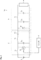
- Fig. 1 is a diagram illustrating structure of a power-conversion system including a resonance-type power converter according to the first embodiment.
- the power-conversion system 10 according to the first embodiment is used for hybrid vehicles capable of driving using a motor as a drive source, and electric vehicles driving using a motor as a drive source, etc.
- situations where the power-conversion system 10 is used are not particularly limited.
- the power-conversion system 10 is a system for supplying DC power of an input-voltage source 1 converted by the DC-DC converter to a load 4.
- the DC-DC converter is configured by an inverter 2 and a rectifier 3, and performs control of output power according to a supply state of the power to the load 4.
- the input-voltage source 1 generates and outputs DC power.
- the input-voltage source 1 rectifies AC voltage (for example, 200V) input from a commercial power supply by a rectifier circuit (not shown in the figure), and converts to DC voltage by smoothing with a smoothing circuit (not shown in the figure). Then, conversion to DC voltage of the predetermined target voltage is performed by DC-DC converter (not shown in the figure).
- the structure of the input-voltage source 1 is not limited and any structure capable of outputting predetermine DC voltage can be used.
- the inverter 2 convers DC voltage input from the input-voltage source 1 to AC voltage.
- the inverter 2 is a so-called class-E inverter that includes an input coil L c , a switching element S, a shunt capacitor C s , and a series resonant circuit consisting of a capacitor C 0 and a coil L 0 ,.
- the input coil L c is connected in series between an output terminal on a higher potential side of the input-voltage source 1 and a switching element S. Specifically, one end of the input coil L c is connected to the input-voltage source 1 and the other end of the input coil L c is connected to the switching element S. Since the input-voltage source 1 outputs certain DC voltage, the input coil L c supplies certain DC current to the switching element S.
- the input coil L c is a so-called choke coil.
- the switching element S switches an ON state and an OFF state according to a control signal input from the controller 5.
- the switching element S is explained as a Metal Oxide Semiconductor Field Effect Transistor (MOSFET), but the switching element S is not particularly limited.
- the switching element S may be, for example, a bipolar transistor controllable by current, or Insulated Gate Bipolar Transistor (IGBT) controllable by voltage, etc.
- a drain terminal of the switching element S is connected to the other end of the input coil L c .
- a source terminal of the switching element S is connected to an output terminal on a lower potential side of the input-voltage source 1.
- a control signal from the controller 5 is input.
- the control signal is a pulse signal that repeats a high level and a low level at a predetermined frequency.
- the predetermined frequency is a frequency for switching the switching element S, and in the following, also called as switching frequency f s .
- a diode that connects to the switching element S in parallel may be arranged.
- a structure connecting an anode terminal of a diode to the source terminal of the switching element S and connecting a cathode terminal of the diode to the drain terminal of the switching element S may be used.
- the shunt capacitor C s is a capacitor parallelly connected to the switching element S and that accumulates electric energy when the switching element S is in an OFF state. Then, after voltage at both ends the shunt capacitor C s reaches a peak, discharge is performed, and electric energy is released. At a timing voltage at both ends of the shunt capacitor C s reaches zero voltage, a state of the switching element S switches from the OFF state to ON state. Control of the switching element S by the controller 5 will be described in the following.
- the coil L 0 and the capacitor C 0 are the series resonant circuit designed so that their resonance frequency matches with a switching frequency f s ..
- One end of the coil L 0 is connected to the drain terminal of the switching element S and the other end of the input coil L c .
- the other end of the coil L 0 is connected to the other end of the capacitor C 0 .
- the other end of the capacitor C 0 is connected to the rectifier 3 described later.
- the series resonant circuit consisting of the coil L 0 and capacitor C 0 are explained as a resonant circuit. Because of the resonance characteristics of the resonant circuit, output voltage of the inverter 2 is represented by the shape of a sinusoidal wave whose period is a resonance frequency (switching frequency f s ).
- the rectifier 3 is arranged to an output side of the inverter 2 and converts the AC voltage output from the inverter 2 to DC voltage.
- the rectifier 3 includes a diode D, a shunt capacitor C d , coil L f , and capacitor Cf, and is a so-called class-E rectifier.
- the diode D is a diode that functions as a switching element. An anode terminal of the diode D is connected to the other end of the capacitor C 0 and a cathode terminal of the diode D is connected to an output terminal on the lower potential side of the input-voltage source 1.
- the shunt capacitor C d is parallelly connected to the diode D.
- the coil L f and the capacitor Cf configures a low pass filter.
- One end of the coil L f is connected to the other end of the capacitor C 0 , the anode terminal of the diode D, and one end of the shunt capacitor C d .
- the capacitor Cf is parallelly connected to the shunt capacitor C d .
- One end of the capacitor Cf is connected to the other end of the coil L f , and the other end of the capacitor Cf is connected to the output terminal on the lower potential side of the input-voltage source 1.
- the diode D performs half-rectifying operation and voltage rectified by the Diode D is converted to DC voltage by the low pass filter.
- the DC voltage of the input-voltage source 1, converted by the DC-DC converter, is input to the load 4.
- the load 4 for example, is a battery including a secondary battery or the like.
- the load 4 is explained as a battery.
- the load 4 is not limited to a battery, and any that can accumulate DC power from the input-voltage source 1, or drivable by the DC power may be used.
- the controller 5 includes a microcomputer including a Central Processing Unit (CPU), a Read Only Memory (ROM), and a Random Access Memory (RAM), and a Field-Programmable Gate Array (FPGA).
- CPU Central Processing Unit
- ROM Read Only Memory
- RAM Random Access Memory
- FPGA Field-Programmable Gate Array
- the controller 5 controls output power of the DC-DC converter. Specifically, the controller 5 generates a control signal for turning on and off the switching element S, and outputs to the gate terminal of the switching element S. For example, the controller 5 generates a pulse signal of the switching frequency f s based on a reference clock, amplifies the pulse signal to level capable of driving the switching element S in a drive circuit (not shown in the figure), and outputs to the gate terminal of the switching element S as a control signal. In this way, the switching element S is turned on or turned off.
- “turnon” is an operation in which the switching element S switches from an OFF state to an ON state
- an “turn-off” is an operation an operation in which the switching element S switches from an ON state to an OFF state.
- the detected value is input to the controller 5.
- the controller 5 performs feedback control based on an output current value. For example, based on the output current value, the controller 5 changes and adjusts frequency and duty ratio on the control signal. This allows the switching frequency f s and duty ratio of the switching element S to be changed to control the output power of the DC-DC converter.
- the duty ratio is a value indicating a ratio of an on period to a unit period when an on and off periods of the switching element S are defined as a unit period.
- the controller 5 generates a control signal that turns on the switching element S in a state where the voltage between the drain terminal and source terminal of the switching element S is zero voltage.
- the switching element S has an on-resistance between the drain terminal and source terminal due to its internal structure. For this reason, when the switching element switches from an OFF state to ON state in a state the predetermined voltage is applied between both terminals of the switching element, power consumption due to the voltage between both terminals of the switching element and the on-resistance generates and the power-conversion efficiency of the inverter is reduced (also called as a switching loss).
- the applied voltage between the drain terminal and the source terminal of the switching element S is represented by a sinusoidal voltage that varies over time due to the resonant characteristics of the resonant circuit.. For this reason, for example, when the switching element S is turned on in a state where the voltage between the drain terminal and source terminal is zero voltage, power consumption generated by the switching element S is greatly reduced, improving power-conversion efficiency of the inverter
- ZVS Zero Voltage Switching
- soft switching operation of ZVS or the like includes operation in which the switching element S turns is turned off in a state where the voltage between the drain terminal and source terminal is zero voltage.
- the controller 5 controls a timing of turning on the switching element when performing soft switching of the switching element S. Specifically, as shown in Fig. 2 , the controller 5 generates a control signal so as to delay turn on of the switching element S for the predetermined delay time T d (T d >0) after the voltage between the drain terminal and source terminal reaches zero voltage due to sinusoidal voltage. At the timing when the switching element is turned on, the voltage at both ends of the switching element is maintained at zero voltage.
- Fig. 2 is an example of a control signal output by the controller 5.
- Fig. 2(A) illustrates a control signal output by the controller 5 to the gate terminal of the switching element S
- Fig. 2(B) illustrates voltage V ds between the drain terminal and source terminal of the switching element S.
- a method for controlling delay time T d a method of changing frequency of the control signal, a method of changing a duty ratio of the control signal, or a combination of these methods may be mentioned.
- the controller 5 reads the delay time T d corresponding to the output current value and changes the frequency and duty ratio. For example, when the duty ratio of the control signal is reduced, the off period increases to the extent that the on period decreases. As a result, the timing of the switching element S switching from off to on can be delayed and the delay time T d can be increased. Conversely, when the duty ratio of the control signal is increased, the timing of the switching element S switching from off to on can be earlier and the delay time T d can be reduced.
- the controller 5 secures the delay time T d in a range of a predetermined switching frequency f s . Specifically, the controller 5 secures the delay time T d in a range where the switching frequency f s is higher than a series resonance frequency f r1 (f s >f r1 ).
- the series resonance frequency f r1 is a resonance frequency of the resonant circuit consisting of the coil L 0 and capacitor C 0 when the switching element S is in an ON state and can be represented by the following formula (1).
- ⁇ r 1 1 2 ⁇ L 0 C 0 [Numeral 1]
- f r1 represents a value of the series resonance frequency f r1
- L 0 represents a value of inductance of the coil L 0
- C 0 represents a value of the capacity of the capacitor C 0 .
- Fig. 3 is an example of a relationship between the output current of the DC-DC converter and frequency of the switching element according to the reference example.
- Fig. 3 is an example of using a battery as a load (corresponds to the load 4 in the present embodiment) and shows characteristics of each state of SOC. Incidentally, the state of SOC is shown in three levels according to the value of SOC (high SOC, middle SOC, and low SOC).
- the DC-DC converter according to the reference example has a same configuration except that the controller does not include a function for securing the delay time T d compared to the DC-DC converter according to the present embodiment.
- output power is controlled by controlling the switching frequency.
- the controller of the reference example when charging a battery at a maximum output current (in case of heavy load), the controller of the reference example generates a control signal such that the switching frequency f s is a frequency f 1 .
- the controller of the reference example controls the frequency of a control signal higher than the frequency f 1 .
- the controller of the reference example generates a control signal such that the switching frequency f s is a frequency f 2 (>frequency f 1 ).
- Fig. 4 is a figure corresponding to Fig. 3 and shows an example of a relationship between the switching frequency f s and soft switching in the reference example.
- Fig. 4(A) illustrates operation of the switching element in the reference example at the frequency f 1 shown in Fig. 3
- Fig. 4(B) illustrates operation of the switching element in the reference example at the frequency f 2 shown in Fig. 3 .
- (a) to (c) illustrate states of the switching element of the reference example.
- (a) illustrates gate voltage V gate
- (b) illustrates voltage V ds between the drain terminal and source terminal
- (c) illustrates drain current I d .
- the controller of the reference example In the case of heavy load, the controller of the reference example generates a control signal corresponding to the frequency f 1 illustrated in Fig. 3(A) and outputs to the switching element. In this case, as shown in Fig. 4(A) , after the voltage V ds reaches zero voltage, the gate voltage V gate begins to rise.
- the drain current I d does not flow when the gate voltage V gate begins to rise, and the switching element of the reference example performs soft switching.
- the controller of the reference example in the case of light load, the controller of the reference example generates a control signal corresponding to the frequency f 2 shown in Fig. 3(B) and outputs to the switching element in order to reduce the output current.
- the frequency of the control signal is higher than the frequency f 1
- the timing of the switching element switching from off to on is earlier compared to the timing in the case of frequency f 1 .becomes earlier compared to the timing when the frequency of the control is frequency f 1 .
- the gate voltage V gate rises.
- Drain current I d flows with the gate voltage V gate begins to rise, and the switching element of the reference example cannot perform operation of soft switching. This is because the controller of the reference example simply increased the frequency of the control signal to reduce the output current without securing the delay time T d .
- the controller of the reference example does not secure the delay time T d , the switching element can only perform operation of soft switching within a range of switching frequency f s , and power-conversion efficiency cannot be improved.
- the controller of the present embodiment secures the delay time T d in a predetermined range of switching frequency f s (f s >f r1 ), as described above. This allows the switching element S to operate soft switching in a wide range of the switching frequency f s compared to the DC-DC converter of the reference example. As a result, power-conversion efficiency can be improved.
- FIG. 5 is an example showing a relationship between the delay time T d and the applied voltage to the switching element S.
- Fig. 5(A) illustrates operation of the switching element when the delay time T d is greater than zero
- Fig. 5(B) illustrates operation of the switching element when the delay time T d is around zero (T d ⁇ 0).
- (a) to (c) illustrate states of the switching element.
- (a) illustrates the gate voltage V gate
- (b) illustrates voltage V ds between the drain terminal and source terminal
- (c) illustrates drain current I d .
- each DC-DC converter outputs the same output power.
- Non-patent Document 1 Technical Group on Nonlinear Problems, The Institute of Electronics, Information and Communication Engineers (IEICE), vol.114, no.414, pp.143-146, Jan. 2015 ).
- IEICE Institute of Electronics, Information and Communication Engineers
- the maximum voltage value of the voltage V ds is voltage V 2 when the delay time T d is around zero, as shown in Fig. 5(B) .
- the maximum voltage value of the voltage V ds is voltage V 1 that is lower than the voltage V 2 (V 1 ⁇ V 2 ) when the delay time T d is greater than zero, as shown in Fig. 5(A) .
- the voltage V ds between the drain terminal and source terminal of the switching element S also called as applied voltage to the switching element S
- the controller 5 sets the delay time within a range shown in the following formula (2) according to the load 4 or other circuit designs. [Numeral 2] 0 ⁇ T d ⁇ 1 2 ⁇ s
- T d represents a value of the delay time T d
- f s represents a switching frequency of the switching element S.
- the delay time T d is secured, and the switching element S is turned on within the delay time T d .
- This can expand a range of the switching frequency f s capable of soft switching and improve the power-conversion efficiency of the DC-DC converter.
- the applied voltage to the switching element S can be suppressed, the element with a low withstand voltage can be included in the selection target when the switching element S is selected, and the cost of the DC-DC converter can be reduced.
- the switching frequency f s is a frequency higher than the series resonance frequency f r1
- delay time T d can be secured. This allows the switching element S to perform soft switching while suppressing the applied voltage to the switching element S, even when the switching frequency f s is increased to reduce output power of the DC-DC converter. As a result, the cost and efficiency of the DC-DC converter can be reduced and improved.
- a detected value is acquired from a current sensor that detects the output current of the DC-DC converter, and a delay time T d is secured based on the output current value. This allows the cost of the DC-DC converter to be reduced without the need to provide a high-precision current sensor around the switching element S to detect the drain current of the switching element S.
- Fig. 6 is an example of a method for controlling the DC-DC converter according to the second embodiment.
- the controller 15 reduces the output power of the DC-DC converter while securing that delay time T d is greater than or equal to a predetermined value by controlling the switching frequency f s when the switching frequency f s satisfies the following formula (3).
- ⁇ r 1 ⁇ ⁇ s ⁇ ⁇ r 2 [Numeral 3]
- f s represents a value of the switching frequency of the switching element S
- f r1 represents a value of a series resonance frequency (see the above formula (1))
- f r2 represents a frequency value of a parallel resonance frequency.
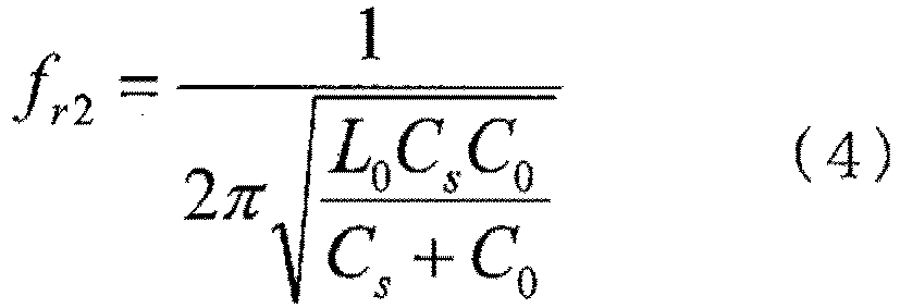
- the parallel resonance frequenczy f r2 is a resonance frequency in the OFF state of the switching element S, which is the resonant frequency of the resonant circuit consisting of the coil L 0 , the capacitor C 0 , and shunt capacitor C s , and is shown in formula (4) below.
- f r2 represents a value of a parallel resonance frequency
- L 0 represents an inductance value of the coil L 0
- C s represents a value of the capacity of the shunt capacitor C s .
- Fig. 6(b) is an example showing a relationship between the delay time T d and the switching frequency f s
- Fig. 6(c) is an example showing a relationship between the output power and the switching frequency f s of the DC-DC converter.
- the controller 15 sets a duty ratio when starting the control (for example, D U1 ) in order to make the delay time T d secure predetermined time even when the switching frequency f s is increased to a parallel resonance frequency f r2 .
- the controller 15 estimates a delay time T d capable of soft switching when the switching frequency f s is a parallel resonance frequency f r2 .
- the controller 15 can set a duty ratio when starting the control by calculating a delay time delay time T d when starting the control based on the estimated result.
- the controller 15 fixes the duty ratio to D U1 and increases the switching frequency f s from a series resonance frequency f r1 to the parallel resonance frequency f r2 by step-wisely increasing the frequency of the control signal in a fixed period unit based on the output current value.
- Fig. 6(b) shows that the delay time T d is reduced from a time T 1 to a time T 2 ( ⁇ T 1 ) according to the switching frequency f s when the switching frequency f s is increased from the series resonance frequency f r1 to the parallel resonance frequency f r2 .
- Each of the time T 1 and the time T 2 is a time that satisfy the above formula (2).
- the constant period of increasing the frequency (corresponding to the slope shown in Fig. 6(b) ) is preferably set accordingly based on the output current value.
- Fig. 6(c) shows that the output power reduces from power W 1 to power W 2 ( ⁇ Wi) when the switching frequency f s is increased from the series resonance frequency f r1 to the parallel resonance frequency f r2 .
- the controller 15 controls a duty ratio when the switching frequency f s satisfies the following formula (5) as a result of step-wisely increasing the frequency of the control signal.
- the controller 15 reduces the output power of the DC-DC converter while securing the delay time T d greater than or equal to a predetermined value.
- f s represents a value of the switching frequency of the switching element
- f r2 represents a value of the frequency of the parallel resonance frequency f r2 (see the above formula (4)).
- Fig. 6(d) is an example showing a relationship between the delay time T d and duty ratio
- Fig. 6(e) is an example of a relationship between the output power and duty ratio of the DC-DC converter.
- the controller 15 fixes the switching frequency f s to a predetermined frequency value (for example, switching frequency f s ⁇ f r2 ), and further reduces the output power of the DC-DC converter by step-wisely decreasing the duty ratio.
- Fig. 6(d) shows that the delay time T d increases from time T 2 to time T 3 (>T 2 ) according to the duty ratio when the duty ratio is reduced from D U1 to D U2 .
- Time T 3 is a value that satisfies the above formula (2).
- the constant period of reducing the duty ratio (corresponding to the slope shown in Fig. 6(d) ) is preferably set accordingly based on the output current value.
- Fig. 6(e) shows that the output power decreases from power W 2 to power W 3 ( ⁇ W 2 ) according to the duty ratio when the duty ratio is decreased from D U1 to D U2 .
- the switching frequency f s when the switching frequency f s satisfies the above formula (3), by fixing the duty ratio to a predetermined value and also increasing the switching frequency f s , the output power of the DC-DC converter is reduced. Then, when the increased switching frequency f s satisfies the above formula (5), the switching frequency f s is fixed to a value around the parallel resonance frequency f r2 and by reducing the duty ratio, the output power of the DC-DC converter is reduced. As shown in Fig. 7 , this allows the applied voltage to the switching element S to be suppressed compared to the DC-DC converter of the reference example, even when the output power of the DC-DC converter is reduced. Incidentally, Fig.
- FIG. 7 is an example showing a relationship between the output power of the DC-DC converter according to the second embodiment and the applied voltage to the switching element S.
- Fig. 7 shows a relationship between the output power of the DC-DC converter where the delay time T d is not secured and the applied voltage to the switching element S in a dotted line as a reference example.
- a duty ratio when starting control of the switching frequency f s is set so that the delay time T d is secured for a predetermined time even when the switching frequency f s is increased to the parallel resonance frequency f r2 This prevents unnecessary control of the duty ratio to secure the delay time T d in the range of frequencies until the switching frequency f s reaches the parallel resonance frequency f r2 .
- the switching element S can be made to operate soft switching and the applied voltage to the switching element S can be suppressed.
- Fig. 8 is an example of a method for controlling the DC-DC converter according to the third embodiment.
- the output power of the DC-DC converter is reduced in the order control opposite to the order of control described in the second embodiment. In other words, in the present embodiment, first, the output power is reduced by controlling the duty ratio and then the output power is reduced by controlling frequency.
- the controller 25 reduces the output power of the DC-DC converter while securing the delay time T d .
- Fig 8(b) is an example of a relationship between the delay time T d and duty ratio
- Fig. 8(e) is an example of a relationship between the output power and duty ratio of the DC-DC converter.
- the controller 25 fixes the switching frequency to a predetermined frequency value (for example, switching frequency f s ⁇ f r1 ), and step-wisely reduces the output power of the DC-DC converter by step-wisely decreasing the duty ratio.
- Fig. 8(b) shows that the delay time T d increases from time T 1 to time T 2 (>T 1 ) according to the duty ratio when the duty ratio is reduced from D U1 to D U2 .
- Each of time T 1 and time T 2 is a value that satisfy the above formula (2).
- the constant period of decreasing the duty ratio (corresponding to the slope shown in Fig. 8(b) ) is preferably set accordingly based on the output current value.
- Fig. 8(c) shows that the output power reduces from power W 1 to power W 2 ( ⁇ Wi) according to the duty ratio when the duty ratio is reduced form the duty ratio D U1 to D U2 .
- the controller 25 fixes the duty ratio to a predetermined value (for example, duty ratio D U2 ), and further reduces the output power of the DC-DC converter by step-wisely increasing the switching frequency f s .
- Fig. 8(d) shows that the output power decreases from the power W 2 to power W 3 ( ⁇ W 2 ) according to the switching frequency f s .
- the frequency f start represents a frequency set again when starting the frequency control.
- the frequency f start is the frequency for making the output power the DC-DC converter when starting the frequency control to the same power as the output power of the DC-DC converter when finishing the duty ratio control.
- Fig. 8(e) shows that the output power reduces form the power W 2 to power W 3 ( ⁇ W 2 ) according to the switching frequency f s when the switching frequency f s is increased from the frequency f start to the parallel resonance frequency f r2 .
- the switching frequency f s when the switching frequency f s satisfies the above formula (3), the switching frequency f s is fixed to a predetermined frequency and the output power of the DC-DC converter is reduced by reducing the duty ratio. Then, when the duty ratio reduces to the predetermined value, by fixing the duty ratio and increasing the switching frequency f s , the output power of the DC-DC converter is reduced.
- the noise generated by the switching of the switching element S, or the so-called switching noise to be predicted because the switching frequency fs is fixed at heavy load. As a result, the design of the noise filter can be simplified.
- Fig. 9 is an example of a method for controlling the DC-DC converter according to the fourth embodiment.
- the controller 35 when reducing the output the power of the DC-DC converter, the controller 35 repeatedly performs a frequency control for controlling the switching frequency f s and duty ratio control for controlling the duty ratio of the switching element S. Specifically, the controller 35 fixes the duty ratio and increases the switching frequency f s in the frequency control, and fixes the switching frequency f s and decreases the duty ratio in the duty ratio control. Also, the controller 35 performs each control in a range of switching frequency f s that is from a series resonance frequency f r1 to around the parallel resonance frequency f r2 . Additionally, the controller 35 performs each control so as to make the delay time T d satisfy the above formula (2).
- a control method shown in Fig. 9(a) to Fig. 9(d) is explained.
- the controller 35 may reduce the output power by starting with frequency control, then performing duty ratio control, and finally performing frequency control.
- the controller 35 may reduce the output power by starting with frequency control, then performing in the order of duty ratio control and frequency control, and finally performing duty ratio control.
- the controller 35 may reduce the output power by starting with duty ratio control, then performing frequency control, and finally performing duty ratio control.
- Fig. 9(c) the controller 35 may reduce the output power by starting with duty ratio control, then performing frequency control, and finally performing duty ratio control.
- the controller 35 may reduce the output power by starting with duty ratio control, then performing in the order of frequency control and duty ratio control, and finally performing frequency control.
- the control method shown in Fig. 9(a) to Fig. 9(d) is an example of a method for repeatedly performing frequency control and duty ratio control, and the number of times of frequency control and duty ratio control is not limited. If the delay time T d satisfies the above formula (2), the number of times of each control may be increased than the number of times of each control shown in Fig. 9(a) to Fig. 9(d) .
- the output power of the DC-DC converter is reduced by alternately repeating increase of the switching frequency f s while fixing the duty ratio and decrease of the duty ratio while fixing the switching frequency f s , the output power of the DC-DC converter is reduced.
- This allows soft switching to be performed in accordance with the application over a wide range of switching frequency f s while controlling the applied voltage to the switching element S, even if the application using the power-conversion system 10 is changed.
- the cost and efficiency of the DC-DC converter can be reduced and improved in various applications.
- a resonance-type power converter mounted on a DC-DC converter has been described as an example, but the present invention is not limited to the same.
- a DC-AC inverter configured only by an inverter 2 without a rectifier 3 may be used.
- a rectifier 3 a class-E rectifier circuit is used as an example, however, the rectifier is not limited thereto and a full-wave rectifier circuit may be used. This enables the rectification action to be realized with a generalpurpose and simple circuit configuration, thus further lowering the cost of the resonance-type power converter.
- the rectifier 3 may be a synchronous rectifier circuit.
- a method for securing a delay time T d based on a detected value from the current sensor detecting the output current of the DC-DC converter is used as an example, the invention is not limited thereto. Any value that has correlation with the applied voltage to the switching element S can be used.
- a voltage sensor that detects the voltage V ds between the drain terminal and source terminal of the switching element S may be provided around the switching element S, and a delay time T d may be secured based on the detected value of the voltage sensor. Since the delay time T d is secured based on the applied voltage to the switching element S itself, it can respond even if a load is unexpectedly applied to the switching element S for some reason. As a result, the load on the switching element S can be reduced, even for events that occur suddenly.
- a voltage sensor that detects voltage at both ends of the shunt capacitor C s may be provided, and a delay time T d may be secured based on the detected value of the voltage sensor. Since the voltage sensor detects voltage between both terminals of the switching element S without being affected by the parasitic inductance possessed with the switching element S, the applied voltage to the switching element S can be suppressed without depending on the structure of the switching element S.
- the delay time T d may be secured using a parameter that varies according to the output power.
- the delay time Td can be secured by using a map that shows a relationship between the parameters of the load and the applied voltage of the switching element S.
- the delay time T d is secured by controlling the switching frequency f s and duty ratio is described as an example, but the delay time T d may be secured by controlling either one of the switching frequency f s or the duty ratio.
- the delay time T d capable of soft switching may be estimated and the delay time T d when starting the frequency control may be calculated based on the estimated result. Then, the duty ratio may be set based on the calculated result. This allows soft switching over a wide range of switching frequency fs because the delay time Td can be secured for a predetermined period of time even if the frequency is increased to the parallel resonance frequency fr2, and the applied voltage to the switching element S can be suppressed.
- the maximum and minimum duty ratios corresponding to the maximum and minimum controllable output power values may be calculated. Then, the duty ratio may be controlled within the range of the calculated results to secure the delay time T d .
- the method for controlling the delay time Td is selected appropriately in accordance with a type or characteristics of the load 4 and the situation in which the power-conversion system 10 is used.
- the resonance-type power converter according to the present invention has been described using inverter 2 as an example, however, the present invention is not limited thereto.
- the switching element according to the present invention has been described using the switching element S as an example, however, the present invention is not limited thereto. Further variations and modifications are possible within the scope of the appended claims.
Landscapes
- Engineering & Computer Science (AREA)
- Power Engineering (AREA)
- Dc-Dc Converters (AREA)
Description
- The present invention relates to a method for controlling a resonance-type power converter, a resonance-type power converter, and a DC-DC converter.
- A control device of a resonance DC-DC converter including, based on a determined control amount, a frequency modulation control means for performing frequency modulation control of a semiconductor switching element at a frequency lower than a resonance frequency of a series resonant circuit, a fixed-frequency control means for performing fixed-frequency control by pulse-width modulation control or phase modulation control of a semiconductor switching element at the resonance frequency, and a pulse distribution means for generating driving pulse of the semiconductor switching element based on an output of the frequency modulation control means and fixed-frequency control means is known (Patent Document 1). Furthermore,
Patent Document 2 describes a dual resonance circuit, where the switches of a dual-transistor pushpull configuration are operated under Zero Voltage Switching, ZVS, conditions. The switching frequency is variable between a lower resonance frequency and an upper resonance frequency. The switching is carried out based either on pulse frequency modulation, PFM, or pulse width modulation, PWM. -
- [Patent Document 1]
WO 2013/114758 A - [Patent Document 2]
US2017214278 - In a prior art, there is a problem that a switching loss increases since soft switching cannot be performed when output power is reduced by increasing switching frequency of the switching element.
- A problem to be solved by the present invention is to provide a method for controlling a resonance-type power converter capable of enhancing efficiency of the resonance-type power converter by expanding a range of switching frequency capable of soft switching, a resonance-type power converter, and a DC-DC converter.
- The above problem is solved by the features of
method claim 1 and device claim 8. The dependent claims recite advantageous embodiments of the invention. - According to the present invention, efficiency of a resonance-type power converter can be enhanced.
-
-
Fig. 1 is a diagram of a power-conversion system including a resonance-type power converter according to a first embodiment. -
Fig. 2 is an example of a control signal output by a controller. -
Fig. 3 is an example of a relationship between output current of a DC-DC converter and a frequency of a switching element according to a reference example. -
Fig. 4 is an example of a relationship between switching frequency and soft switching in the reference example. -
Fig. 5 is an example of a relationship between delay time and applied voltage to a switching element. -
Fig. 6 is an example of a method for controlling the DC-DC converter according to a second embodiment. -
Fig. 7 is an example of a relationship between output power of the DC-DC converter according to the second embodiment and applied voltage to the switching element. -
Fig. 8 is an example of a method for controlling the DC-DC converter according to a third embodiment. -
Fig. 9 is an example of a method for controlling the DC-DC converter according to a fourth embodiment. - In the following, embodiments of the present invention will be explained with reference to the drawings.
-
Fig. 1 is a diagram illustrating structure of a power-conversion system including a resonance-type power converter according to the first embodiment. The power-conversion system 10 according to the first embodiment is used for hybrid vehicles capable of driving using a motor as a drive source, and electric vehicles driving using a motor as a drive source, etc. Incidentally, situations where the power-conversion system 10 is used are not particularly limited. - As shown in
Fig. 1 , the power-conversion system 10 is a system for supplying DC power of an input-voltage source 1 converted by the DC-DC converter to a load 4. The DC-DC converter is configured by aninverter 2 and arectifier 3, and performs control of output power according to a supply state of the power to the load 4. - The input-
voltage source 1 generates and outputs DC power. For example, the input-voltage source 1 rectifies AC voltage (for example, 200V) input from a commercial power supply by a rectifier circuit (not shown in the figure), and converts to DC voltage by smoothing with a smoothing circuit (not shown in the figure). Then, conversion to DC voltage of the predetermined target voltage is performed by DC-DC converter (not shown in the figure). Incidentally, the structure of the input-voltage source 1 is not limited and any structure capable of outputting predetermine DC voltage can be used. - The
inverter 2 convers DC voltage input from the input-voltage source 1 to AC voltage. Theinverter 2 is a so-called class-E inverter that includes an input coil Lc, a switching element S, a shunt capacitor Cs, and a series resonant circuit consisting of a capacitor C0 and a coil L0,. - The input coil Lc is connected in series between an output terminal on a higher potential side of the input-
voltage source 1 and a switching element S. Specifically, one end of the input coil Lc is connected to the input-voltage source 1 and the other end of the input coil Lc is connected to the switching element S. Since the input-voltage source 1 outputs certain DC voltage, the input coil Lc supplies certain DC current to the switching element S. The input coil Lc is a so-called choke coil. - The switching element S switches an ON state and an OFF state according to a control signal input from the controller 5. In the present embodiment, the switching element S is explained as a Metal Oxide Semiconductor Field Effect Transistor (MOSFET), but the switching element S is not particularly limited. The switching element S may be, for example, a bipolar transistor controllable by current, or Insulated Gate Bipolar Transistor (IGBT) controllable by voltage, etc. A drain terminal of the switching element S is connected to the other end of the input coil Lc. A source terminal of the switching element S is connected to an output terminal on a lower potential side of the input-
voltage source 1. To a gate terminal of the switching element S, a control signal from the controller 5 is input. The control signal is a pulse signal that repeats a high level and a low level at a predetermined frequency. The predetermined frequency is a frequency for switching the switching element S, and in the following, also called as switching frequency fs. When the control signal is at a low level, the switching element S becomes an OFF state and when the control signal is at a high level, the switching element S becomes an ON state. - Incidentally, when a function for operating diode is not available inside the switching element S, a diode that connects to the switching element S in parallel may be arranged. For example, a structure connecting an anode terminal of a diode to the source terminal of the switching element S and connecting a cathode terminal of the diode to the drain terminal of the switching element S may be used. By arranging such diode, the switching element S can be protected from a counter-electromotive force generated along with switching by the switching element S.
- The shunt capacitor Cs is a capacitor parallelly connected to the switching element S and that accumulates electric energy when the switching element S is in an OFF state. Then, after voltage at both ends the shunt capacitor Cs reaches a peak, discharge is performed, and electric energy is released. At a timing voltage at both ends of the shunt capacitor Cs reaches zero voltage, a state of the switching element S switches from the OFF state to ON state. Control of the switching element S by the controller 5 will be described in the following.
- The coil L0 and the capacitor C0 are the series resonant circuit designed so that their resonance frequency matches with a switching frequency fs.. One end of the coil L0 is connected to the drain terminal of the switching element S and the other end of the input coil Lc. The other end of the coil L0 is connected to the other end of the capacitor C0. The other end of the capacitor C0 is connected to the
rectifier 3 described later. Hereafter, for convenience of explanation, the series resonant circuit consisting of the coil L0 and capacitor C0 are explained as a resonant circuit. Because of the resonance characteristics of the resonant circuit, output voltage of theinverter 2 is represented by the shape of a sinusoidal wave whose period is a resonance frequency (switching frequency fs). - The
rectifier 3 is arranged to an output side of theinverter 2 and converts the AC voltage output from theinverter 2 to DC voltage. Therectifier 3 includes a diode D, a shunt capacitor Cd, coil Lf, and capacitor Cf, and is a so-called class-E rectifier. - The diode D is a diode that functions as a switching element. An anode terminal of the diode D is connected to the other end of the capacitor C0 and a cathode terminal of the diode D is connected to an output terminal on the lower potential side of the input-
voltage source 1. - The shunt capacitor Cd is parallelly connected to the diode D.
- The coil Lf and the capacitor Cf configures a low pass filter. One end of the coil Lf is connected to the other end of the capacitor C0, the anode terminal of the diode D, and one end of the shunt capacitor Cd. The capacitor Cf is parallelly connected to the shunt capacitor Cd. One end of the capacitor Cf is connected to the other end of the coil Lf, and the other end of the capacitor Cf is connected to the output terminal on the lower potential side of the input-
voltage source 1. The diode D performs half-rectifying operation and voltage rectified by the Diode D is converted to DC voltage by the low pass filter. - The DC voltage of the input-
voltage source 1, converted by the DC-DC converter, is input to the load 4. The load 4, for example, is a battery including a secondary battery or the like. In the present embodiment, the load 4 is explained as a battery. Incidentally, the load 4 is not limited to a battery, and any that can accumulate DC power from the input-voltage source 1, or drivable by the DC power may be used. - The controller 5 includes a microcomputer including a Central Processing Unit (CPU), a Read Only Memory (ROM), and a Random Access Memory (RAM), and a Field-Programmable Gate Array (FPGA).
- The controller 5 controls output power of the DC-DC converter. Specifically, the controller 5 generates a control signal for turning on and off the switching element S, and outputs to the gate terminal of the switching element S. For example, the controller 5 generates a pulse signal of the switching frequency fs based on a reference clock, amplifies the pulse signal to level capable of driving the switching element S in a drive circuit (not shown in the figure), and outputs to the gate terminal of the switching element S as a control signal. In this way, the switching element S is turned on or turned off. Incidentally, "turnon" is an operation in which the switching element S switches from an OFF state to an ON state, an "turn-off" is an operation an operation in which the switching element S switches from an ON state to an OFF state.
- In addition, from a current sensor (not shown in figure) that detects output current of the DC-DC converter, the detected value is input to the controller 5. The controller 5 performs feedback control based on an output current value. For example, based on the output current value, the controller 5 changes and adjusts frequency and duty ratio on the control signal. This allows the switching frequency fs and duty ratio of the switching element S to be changed to control the output power of the DC-DC converter. Incidentally, the duty ratio is a value indicating a ratio of an on period to a unit period when an on and off periods of the switching element S are defined as a unit period.
- Further, the controller 5 generates a control signal that turns on the switching element S in a state where the voltage between the drain terminal and source terminal of the switching element S is zero voltage. In general, the switching element S has an on-resistance between the drain terminal and source terminal due to its internal structure. For this reason, when the switching element switches from an OFF state to ON state in a state the predetermined voltage is applied between both terminals of the switching element, power consumption due to the voltage between both terminals of the switching element and the on-resistance generates and the power-conversion efficiency of the inverter is reduced (also called as a switching loss).
- As in the present embodiment, in the
inverter 2 with the resonant circuit consisting of the coil L0 and the capacitor C0, the applied voltage between the drain terminal and the source terminal of the switching element S is represented by a sinusoidal voltage that varies over time due to the resonant characteristics of the resonant circuit.. For this reason, for example, when the switching element S is turned on in a state where the voltage between the drain terminal and source terminal is zero voltage, power consumption generated by the switching element S is greatly reduced, improving power-conversion efficiency of the inverter - In the following explanation, for convenience of explanation, such operation of the switching element S is also called as Zero Voltage Switching (ZVS), zero voltage switching, or soft switching. Incidentally, operation of ZVS or the like includes operation in which the switching element S turns is turned off in a state where the voltage between the drain terminal and source terminal is zero voltage.
- In addition, the controller 5 controls a timing of turning on the switching element when performing soft switching of the switching element S. Specifically, as shown in
Fig. 2 , the controller 5 generates a control signal so as to delay turn on of the switching element S for the predetermined delay time Td (Td>0) after the voltage between the drain terminal and source terminal reaches zero voltage due to sinusoidal voltage. At the timing when the switching element is turned on, the voltage at both ends of the switching element is maintained at zero voltage. Incidentally,Fig. 2 is an example of a control signal output by the controller 5.Fig. 2(A) illustrates a control signal output by the controller 5 to the gate terminal of the switching element S, andFig. 2(B) illustrates voltage Vds between the drain terminal and source terminal of the switching element S. - As a method for controlling delay time Td, a method of changing frequency of the control signal, a method of changing a duty ratio of the control signal, or a combination of these methods may be mentioned. For example, when the preset delay time Td is stored in ROM or RAM according to the detected value from the current sensor, the controller 5 reads the delay time Td corresponding to the output current value and changes the frequency and duty ratio. For example, when the duty ratio of the control signal is reduced, the off period increases to the extent that the on period decreases. As a result, the timing of the switching element S switching from off to on can be delayed and the delay time Td can be increased. Conversely, when the duty ratio of the control signal is increased, the timing of the switching element S switching from off to on can be earlier and the delay time Td can be reduced.
- In addition, in the present embodiment, the controller 5 secures the delay time Td in a range of a predetermined switching frequency fs. Specifically, the controller 5 secures the delay time Td in a range where the switching frequency fs is higher than a series resonance frequency fr1 (fs>fr1). The series resonance frequency fr1 is a resonance frequency of the resonant circuit consisting of the coil L0 and capacitor C0 when the switching element S is in an ON state and can be represented by the following formula (1).

- Wherein, fr1 represents a value of the series resonance frequency fr1, L0 represents a value of inductance of the coil L0, and C0 represents a value of the capacity of the capacitor C0.
- Here, by referencing
Fig. 3 andFig. 4 , a relationship between the method for controlling the output power of the DC-DC converter and soft switching is explained using a reference example.Fig. 3 is an example of a relationship between the output current of the DC-DC converter and frequency of the switching element according to the reference example.Fig. 3 is an example of using a battery as a load (corresponds to the load 4 in the present embodiment) and shows characteristics of each state of SOC. Incidentally, the state of SOC is shown in three levels according to the value of SOC (high SOC, middle SOC, and low SOC). The DC-DC converter according to the reference example has a same configuration except that the controller does not include a function for securing the delay time Td compared to the DC-DC converter according to the present embodiment. - As shown in
Fig. 3 , in general, in a DC-DC converter with a class-E inverter, output power is controlled by controlling the switching frequency. For example, when charging a battery at a maximum output current (in case of heavy load), the controller of the reference example generates a control signal such that the switching frequency fs is a frequency f1. On the other hand, when the output current is reduced from the maximum output current because the charge of the battery, which is the load, is approaching full charge (in case of a light load), the controller of the reference example controls the frequency of a control signal higher than the frequency f1. For example, the controller of the reference example generates a control signal such that the switching frequency fs is a frequency f2(>frequency f1). -
Fig. 4 is a figure corresponding toFig. 3 and shows an example of a relationship between the switching frequency fs and soft switching in the reference example.Fig. 4(A) illustrates operation of the switching element in the reference example at the frequency f1 shown inFig. 3 , andFig. 4(B) illustrates operation of the switching element in the reference example at the frequency f2 shown inFig. 3 . InFigs. 4(A) and 4(B), (a) to (c) illustrate states of the switching element of the reference example. (a) illustrates gate voltage Vgate, (b) illustrates voltage Vds between the drain terminal and source terminal, and (c) illustrates drain current Id. - In the case of heavy load, the controller of the reference example generates a control signal corresponding to the frequency f1 illustrated in Fig. 3(A) and outputs to the switching element. In this case, as shown in
Fig. 4(A) , after the voltage Vds reaches zero voltage, the gate voltage Vgate begins to rise. - The drain current Id does not flow when the gate voltage
Vgate begins to rise, and the switching element of the reference example performs soft switching. - On the other hand, in the case of light load, the controller of the reference example generates a control signal corresponding to the frequency f2 shown in Fig. 3(B) and outputs to the switching element in order to reduce the output current. When the frequency of the control signal is higher than the frequency f1, the timing of the switching element switching from off to on is earlier compared to the timing in the case of frequency f1.becomes earlier compared to the timing when the frequency of the control is frequency f1. In this case, as shown in
Fig. 4(B) , before the voltage Vds reaches zero voltage, that is, before discharge of the electric charge accumulated in a shunt capacitor Cs finishes, the gate voltage Vgaterises. Drain current Id flows with the gate voltage Vgate begins to rise, and the switching element of the reference example cannot perform operation of soft switching. This is because the controller of the reference example simply increased the frequency of the control signal to reduce the output current without securing the delay time Td. - As mentioned above, because the controller of the reference example does not secure the delay time Td, the switching element can only perform operation of soft switching within a range of switching frequency fs, and power-conversion efficiency cannot be improved.
- In contrast, the controller of the present embodiment secures the delay time Td in a predetermined range of switching frequency fs (fs>fr1), as described above. This allows the switching element S to operate soft switching in a wide range of the switching frequency fs compared to the DC-DC converter of the reference example. As a result, power-conversion efficiency can be improved.
- Next, by referencing
Fig. 5 , a relationship between delay time Td and applied voltage to the switching element is explained.Fig. 5 is an example showing a relationship between the delay time Td and the applied voltage to the switching element S.Fig. 5(A) illustrates operation of the switching element when the delay time Td is greater than zero, andFig. 5(B) illustrates operation of the switching element when the delay time Td is around zero (Td≈ 0). InFigs. 5(A) and (B), (a) to (c) illustrate states of the switching element. (a) illustrates the gate voltage Vgate, (b) illustrates voltage Vds between the drain terminal and source terminal, and (c) illustrates drain current Id. Incidentally, inFigs. 5(A) and (B) , each DC-DC converter outputs the same output power. - As a control to operate the switching element S shown in
Fig. 5(B) , for example, control of E2-level DC-DC converter that calculates a switching frequency and duty ratio, makes the switching element soft switching and controls a constant voltage is known (Non-patent Document 1: Technical Group on Nonlinear Problems, The Institute of Electronics, Information and Communication Engineers (IEICE), vol.114, no.414, pp.143-146, Jan. 2015). In the control of the DC-DC converter described inNon-patent Document 1, the switching element operates as shown inFig. 5(B) because the delay time Td is not secured. - Regarding the voltage Vds, comparing
Fig. 5(A) and Fig. 5(B) , the maximum voltage value of the voltage Vds is voltage V2 when the delay time Td is around zero, as shown inFig. 5(B) . In contrast, the maximum voltage value of the voltage Vds is voltage V1 that is lower than the voltage V2 (V1<V2) when the delay time Td is greater than zero, as shown inFig. 5(A) . In other words, by securing the value of the delay time Td greater than zero, the voltage Vds between the drain terminal and source terminal of the switching element S (also called as applied voltage to the switching element S) can be suppressed. This is because, by making the delay time Td greater than zero, the on period of the switching element S is decreased and a charge quantity accumulated to the shunt capacitor Cs is decreased. Incidentally, in the present embodiment, the controller 5 sets the delay time within a range shown in the following formula (2) according to the load 4 or other circuit designs. [Numeral 2]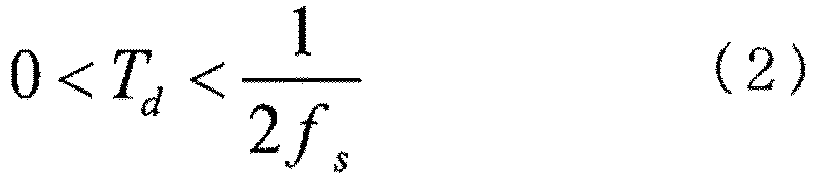
- Wherein, Td represents a value of the delay time Td, and fs represents a switching frequency of the switching element S.
- As mentioned above, in the present embodiment, by controlling at least either one of the switching frequency or the duty ratio of the switching element S, the delay time Td is secured, and the switching element S is turned on within the delay time Td. This can expand a range of the switching frequency fs capable of soft switching and improve the power-conversion efficiency of the DC-DC converter. In addition, since the applied voltage to the switching element S can be suppressed, the element with a low withstand voltage can be included in the selection target when the switching element S is selected, and the cost of the DC-DC converter can be reduced.
- In addition, in the present embodiment, when the switching frequency fs is a frequency higher than the series resonance frequency fr1, by controlling at least either one of the switching frequency or the duty ratio of the switching element S, delay time Td can be secured. This allows the switching element S to perform soft switching while suppressing the applied voltage to the switching element S, even when the switching frequency fs is increased to reduce output power of the DC-DC converter. As a result, the cost and efficiency of the DC-DC converter can be reduced and improved.
- Further, in the present embodiment, a detected value is acquired from a current sensor that detects the output current of the DC-DC converter, and a delay time Td is secured based on the output current value. This allows the cost of the DC-DC converter to be reduced without the need to provide a high-precision current sensor around the switching element S to detect the drain current of the switching element S.
- Next, a method for controlling the DC-DC converter according to the second embodiment will be explained. In the power-conversion system according to the present embodiment, except that the method for controlling the DC-DC converter by the controller 15 differs from the embodiment described above, the same configuration as the DC-DC converter according to the above-mentioned embodiment is included and the explanations in the above embodiment are accordingly referenced.
- Referencing
Fig. 6 , a control method by the controller 15 when reducing the output power of the DC-DC converter will be explained.Fig. 6 is an example of a method for controlling the DC-DC converter according to the second embodiment. As shown inFig. 6(a) ,the controller 15 reduces the output power of the DC-DC converter while securing that delay time Td is greater than or equal to a predetermined value by controlling the switching frequency fs when the switching frequency fs satisfies the following formula (3).

- Wherein, fs represents a value of the switching frequency of the switching element S, fr1 represents a value of a series resonance frequency (see the above formula (1)), and fr2 represents a frequency value of a parallel resonance frequency.
- Further, the parallel resonance frequenczy fr2 is a resonance frequency in the OFF state of the switching element S, which is the resonant frequency of the resonant circuit consisting of the coil L0, the capacitor C0, and shunt capacitor Cs, and is shown in formula (4) below.
- [Numeral 4]
- Wherein, fr2 represents a value of a parallel resonance frequency, L0 represents an inductance value of the coil L0, and Cs represents a value of the capacity of the shunt capacitor Cs.
- Next, a specific control method will be explained using
Fig. 6(b) and Fig. 6(c). Fig. 6(b) is an example showing a relationship between the delay time Td and the switching frequency fs, andFig. 6(c) is an example showing a relationship between the output power and the switching frequency fs of the DC-DC converter. - As shown in
Fig. 6(b) , when the switching frequency fs is higher than the series resonance frequency fr1 and lower than a parallel resonance frequency fr2, the controller 15 fixes the duty ratio to a predetermined value (for example, duty ratio = DU1), and step-wisely reduces the output power of the DC-DC converter by step-wisely increasing the switching frequency fs. - For example, first the controller 15 sets a duty ratio when starting the control (for example, DU1) in order to make the delay time Td secure predetermined time even when the switching frequency fs is increased to a parallel resonance frequency fr2. The controller 15, for example, estimates a delay time Td capable of soft switching when the switching frequency fs is a parallel resonance frequency fr2. The controller 15 can set a duty ratio when starting the control by calculating a delay time delay time Td when starting the control based on the estimated result. Then, when the output power of the DC-DC converter needs to be reduced, the controller 15 fixes the duty ratio to DU1 and increases the switching frequency fs from a series resonance frequency fr1 to the parallel resonance frequency fr2 by step-wisely increasing the frequency of the control signal in a fixed period unit based on the output current value.
Fig. 6(b) shows that the delay time Td is reduced from a time T1 to a time T2(<T1) according to the switching frequency fs when the switching frequency fs is increased from the series resonance frequency fr1 to the parallel resonance frequency fr2. Each of the time T1 and the time T2 is a time that satisfy the above formula (2). The constant period of increasing the frequency (corresponding to the slope shown inFig. 6(b) ) is preferably set accordingly based on the output current value. - In addition, when the switching frequency fs is increased, as shown in
Fig. 6(c) , the output power is reduced as the output current of the DC-DC converter is reduced.Fig. 6(c) shows that the output power reduces from power W1 to power W2 (<Wi) when the switching frequency fs is increased from the series resonance frequency fr1 to the parallel resonance frequency fr2. - Next, a method for controlling the DC-DC converter by the controller 15 after the switching frequency fs reaches the parallel resonance frequency fr2 is explained.
- As shown in
Fig. 6(a) , the controller 15 controls a duty ratio when the switching frequency fs satisfies the following formula (5) as a result of step-wisely increasing the frequency of the control signal. The controller 15 reduces the output power of the DC-DC converter while securing the delay time Td greater than or equal to a predetermined value. - [Numeral 5]

- Wherein, fs represents a value of the switching frequency of the switching element, fr2 represents a value of the frequency of the parallel resonance frequency fr2 (see the above formula (4)).
- Using
Fig. 6(d) and Fig. 6(e) , specific control method will be explained.Fig. 6(d) is an example showing a relationship between the delay time Td and duty ratio, andFig. 6(e) is an example of a relationship between the output power and duty ratio of the DC-DC converter. - When the switching frequency fs reaches around the parallel resonance frequency fr2, as shown in
Fig. 6(d) , the controller 15 fixes the switching frequency fs to a predetermined frequency value (for example, switching frequency fs≈fr2), and further reduces the output power of the DC-DC converter by step-wisely decreasing the duty ratio.Fig. 6(d) shows that the delay time Td increases from time T2 to time T3(>T2) according to the duty ratio when the duty ratio is reduced from DU1 to DU2. Time T3 is a value that satisfies the above formula (2). The constant period of reducing the duty ratio (corresponding to the slope shown inFig. 6(d) ) is preferably set accordingly based on the output current value. - In addition, when the duty ratio is reduced, as shown in
Fig. 6(e) , the output power is reduced as the output current of the DC-DC converter is reduced. This is because, along with decrease in the duty ratio, the on period of the switching element S decreases and a charge quantity accumulated to the shunt capacitor Cs is decreased.Fig. 6(e) shows that the output power decreases from power W2 to power W3(<W2) according to the duty ratio when the duty ratio is decreased from DU1 to DU2. - As mentioned above, in the present embodiment, when the switching frequency fs satisfies the above formula (3), by fixing the duty ratio to a predetermined value and also increasing the switching frequency fs, the output power of the DC-DC converter is reduced. Then, when the increased switching frequency fs satisfies the above formula (5), the switching frequency fs is fixed to a value around the parallel resonance frequency fr2 and by reducing the duty ratio, the output power of the DC-DC converter is reduced. As shown in
Fig. 7 , this allows the applied voltage to the switching element S to be suppressed compared to the DC-DC converter of the reference example, even when the output power of the DC-DC converter is reduced. Incidentally,Fig. 7 is an example showing a relationship between the output power of the DC-DC converter according to the second embodiment and the applied voltage to the switching element S.Fig. 7 shows a relationship between the output power of the DC-DC converter where the delay time Td is not secured and the applied voltage to the switching element S in a dotted line as a reference example. - In addition, in the present embodiment, a duty ratio when starting control of the switching frequency fs is set so that the delay time Td is secured for a predetermined time even when the switching frequency fs is increased to the parallel resonance frequency fr2 This prevents unnecessary control of the duty ratio to secure the delay time Td in the range of frequencies until the switching frequency fs reaches the parallel resonance frequency fr2.In addition, in a wide range of switching frequencies fs, the switching element S can be made to operate soft switching and the applied voltage to the switching element S can be suppressed.
- Next, a method for controlling a DC-DC converter according to a third embodiment will be explained. In the DC-DC converter according to the present embodiment, except that the method for controlling the DC-DC converter by the controller 25 differs from the embodiments described above, the same configuration as the DC-DC converter according to the above-mentioned embodiments is included and the explanations in the above embodiments are accordingly referenced.
- Using
Fig. 8 , a method for controlling the DC-DC converter by the controller 25 when the output power of the DC-DC converter is reduced is explained.Fig. 8 is an example of a method for controlling the DC-DC converter according to the third embodiment. In the present embodiment, the output power of the DC-DC converter is reduced in the order control opposite to the order of control described in the second embodiment. In other words, in the present embodiment, first, the output power is reduced by controlling the duty ratio and then the output power is reduced by controlling frequency. - As shown in
Fig. 8(a) , when the switching frequency fs satisfies the above formula (3), the controller 25 reduces the output power of the DC-DC converter while securing the delay time Td. - Next, specific control method is explained with reference to
Fig. 8(b) and Fig. 8(c). Fig 8(b) is an example of a relationship between the delay time Td and duty ratio, andFig. 8(e) is an example of a relationship between the output power and duty ratio of the DC-DC converter. - As shown in
Fig. 8(b) , when the switching frequency fs is higher than the series resonance frequency fr1 and lower than the parallel resonance frequency fr2, the controller 25 fixes the switching frequency to a predetermined frequency value (for example, switching frequency fs≈fr1), and step-wisely reduces the output power of the DC-DC converter by step-wisely decreasing the duty ratio.Fig. 8(b) shows that the delay time Td increases from time T1 to time T2(>T1) according to the duty ratio when the duty ratio is reduced from DU1 to DU2. Each of time T1 and time T2 is a value that satisfy the above formula (2). The constant period of decreasing the duty ratio (corresponding to the slope shown inFig. 8(b) ) is preferably set accordingly based on the output current value. - In addition, when the duty ratio is reduced, as shown in
Fig. 8(c) , the output power is reduced as the output current of the DC-DC converter is reduced.Fig. 8(c) shows that the output power reduces from power W1 to power W2 (<Wi) according to the duty ratio when the duty ratio is reduced form the duty ratio DU1 to DU2. - Next, a method for controlling the DC-DC converter by the controller 25 after the duty ratio reaches a predetermined value is explained.
- When the duty ratio reaches a predetermined value, as shown in
Fig. 8(d) , the controller 25 fixes the duty ratio to a predetermined value (for example, duty ratio DU2), and further reduces the output power of the DC-DC converter by step-wisely increasing the switching frequency fs..Fig. 8(d) shows that the output power decreases from the power W2 to power W3 (<W2) according to the switching frequency fs. when the switching frequency fs is increased from a frequency fstart to a parallel resonance frequency fr2.Incidentally, the frequency fstart represents a frequency set again when starting the frequency control. The frequency fstart is the frequency for making the output power the DC-DC converter when starting the frequency control to the same power as the output power of the DC-DC converter when finishing the duty ratio control. - In addition, when the switching frequency fs is increased, as shown in
Fig. 8(e) , the output power is reduced as the output current of the DC-DC converter is reduced.Fig. 8(e) shows that the output power reduces form the power W2 to power W3(<W2) according to the switching frequency fs when the switching frequency fs is increased from the frequency fstart to the parallel resonance frequency fr2. - As mentioned above, in the present embodiment, when the switching frequency fs satisfies the above formula (3), the switching frequency fs is fixed to a predetermined frequency and the output power of the DC-DC converter is reduced by reducing the duty ratio. Then, when the duty ratio reduces to the predetermined value, by fixing the duty ratio and increasing the switching frequency fs, the output power of the DC-DC converter is reduced. This allows the noise generated by the switching of the switching element S, or the so-called switching noise, to be predicted because the switching frequency fs is fixed at heavy load. As a result, the design of the noise filter can be simplified.
- Next, a method for controlling a DC-DC converter according to the fourth embodiment is explained. In the power-conversion system according to the present embodiment, except that the method for controlling the DC-DC converter by the controller 35 differs from the embodiments described above, the same configuration as the DC-DC converter according to the above-mentioned embodiments is included and the explanations in the above embodiments are accordingly referenced.
- Referencing
Fig. 9 , a control method by the controller 35 when reducing the output power of the DC-DC converter will be explained.Fig. 9 is an example of a method for controlling the DC-DC converter according to the fourth embodiment. - In the present embodiment, when reducing the output the power of the DC-DC converter, the controller 35 repeatedly performs a frequency control for controlling the switching frequency fs and duty ratio control for controlling the duty ratio of the switching element S. Specifically, the controller 35 fixes the duty ratio and increases the switching frequency fs in the frequency control, and fixes the switching frequency fs and decreases the duty ratio in the duty ratio control. Also, the controller 35 performs each control in a range of switching frequency fs that is from a series resonance frequency fr1 to around the parallel resonance frequency fr2. Additionally, the controller 35 performs each control so as to make the delay time Td satisfy the above formula (2).
- An example of a control method shown in
Fig. 9(a) to Fig. 9(d) is explained. For example, as shown inFig. 9(a) , the controller 35 may reduce the output power by starting with frequency control, then performing duty ratio control, and finally performing frequency control. In addition, for example, as shown inFig. 9(b) , the controller 35 may reduce the output power by starting with frequency control, then performing in the order of duty ratio control and frequency control, and finally performing duty ratio control. Furthermore, for example, as shown inFig. 9(c) , the controller 35 may reduce the output power by starting with duty ratio control, then performing frequency control, and finally performing duty ratio control. In addition, for example, as shown inFig. 9(d) , the controller 35 may reduce the output power by starting with duty ratio control, then performing in the order of frequency control and duty ratio control, and finally performing frequency control. Incidentally, the control method shown inFig. 9(a) to Fig. 9(d) is an example of a method for repeatedly performing frequency control and duty ratio control, and the number of times of frequency control and duty ratio control is not limited. If the delay time Td satisfies the above formula (2), the number of times of each control may be increased than the number of times of each control shown inFig. 9(a) to Fig. 9(d) . - As mentioned above, in the present embodiment, the output power of the DC-DC converter is reduced by alternately repeating increase of the switching frequency fs while fixing the duty ratio and decrease of the duty ratio while fixing the switching frequency fs, the output power of the DC-DC converter is reduced. This allows soft switching to be performed in accordance with the application over a wide range of switching frequency fs while controlling the applied voltage to the switching element S, even if the application using the power-
conversion system 10 is changed. As a result, the cost and efficiency of the DC-DC converter can be reduced and improved in various applications. - Incidentally, the embodiments explained above are described for easy understanding of the present invention, and are not for limiting the present invention. Accordingly, each element disclosed in the embodiments is intended to include all design changes and equivalents that correspond to the technical scope of the present invention.
- For example, in the above-described embodiments, the case of a resonance-type power converter mounted on a DC-DC converter has been described as an example, but the present invention is not limited to the same. For example, a DC-AC inverter configured only by an
inverter 2 without arectifier 3 may be used. - Also, for example, in the above embodiments, as a
rectifier 3, a class-E rectifier circuit is used as an example, however, the rectifier is not limited thereto and a full-wave rectifier circuit may be used. This enables the rectification action to be realized with a generalpurpose and simple circuit configuration, thus further lowering the cost of the resonance-type power converter. Incidentally, therectifier 3 may be a synchronous rectifier circuit. - Furthermore, in the present embodiments, a method for securing a delay time Td based on a detected value from the current sensor detecting the output current of the DC-DC converter is used as an example, the invention is not limited thereto. Any value that has correlation with the applied voltage to the switching element S can be used.
- For example, a voltage sensor that detects the voltage Vds between the drain terminal and source terminal of the switching element S may be provided around the switching element S, and a delay time Td may be secured based on the detected value of the voltage sensor. Since the delay time Td is secured based on the applied voltage to the switching element S itself, it can respond even if a load is unexpectedly applied to the switching element S for some reason. As a result, the load on the switching element S can be reduced, even for events that occur suddenly.
- In addition, a voltage sensor that detects voltage at both ends of the shunt capacitor Cs may be provided, and a delay time Td may be secured based on the detected value of the voltage sensor. Since the voltage sensor detects voltage between both terminals of the switching element S without being affected by the parasitic inductance possessed with the switching element S, the applied voltage to the switching element S can be suppressed without depending on the structure of the switching element S.
- Furthermore, for example, in a load driven according to the output power of the DC-DC converter, the delay time Td may be secured using a parameter that varies according to the output power. In this case, the delay time Td can be secured by using a map that shows a relationship between the parameters of the load and the applied voltage of the switching element S.
- In addition, for example, in the above embodiments, the configuration in which the delay time Td is secured by controlling the switching frequency fs and duty ratio is described as an example, but the delay time Td may be secured by controlling either one of the switching frequency fs or the duty ratio.
- For example, upon starting frequency control, even when the frequency is increased to the parallel resonance frequency fr2, the delay time Td capable of soft switching may be estimated and the delay time Td when starting the frequency control may be calculated based on the estimated result. Then, the duty ratio may be set based on the calculated result. This allows soft switching over a wide range of switching frequency fs because the delay time Td can be secured for a predetermined period of time even if the frequency is increased to the parallel resonance frequency fr2, and the applied voltage to the switching element S can be suppressed.
- Furthermore, for example, when the output power is controlled by duty ratio control, the maximum and minimum duty ratios corresponding to the maximum and minimum controllable output power values may be calculated. Then, the duty ratio may be controlled within the range of the calculated results to secure the delay time Td. The method for controlling the delay time Td is selected appropriately in accordance with a type or characteristics of the load 4 and the situation in which the power-
conversion system 10 is used. - Additionally, for example, in the present description, the resonance-type power converter according to the present invention has been described using
inverter 2 as an example, however, the present invention is not limited thereto. Further, in the present description, the switching element according to the present invention has been described using the switching element S as an example, however, the present invention is not limited thereto. Further variations and modifications are possible within the scope of the appended claims. -
- 10
- power-conversion system
- 1
- input-voltage source
- 2
- inverter
- 3
- rectifier
- 4
- load
- 5
- controller
Claims (8)
- A method for controlling a resonance-type power converter (10),- wherein the resonance-type power converter (10) includes an inverter (2) comprising a resonant circuit (L0, C0, CS) and a rectifier (3) connected to the inverter (2) and is configured to convert power of a DC power source (1) and to output a DC voltage of a predetermined target voltage,- wherein the method comprises:- when a switching frequency (fs ) of a switching element (S) included in the inverter (2) satisfies a following formula (1)
 - turning on the switching element (S) within the delay time (Td),- wherein when the switching frequency (fs ) satisfies a following formula (2),
 - wherein when the switching frequency (fs ) satisfies a following formula (3),
 - wherein, fr1 represents a resonance frequency of the resonant circuit (L0, C0, Cs) in an ON state of the switching element (S), fr2 represents a resonance frequency of the resonant circuit (L0, C0, Cs) in the OFF state of the switching element (S), and fs represents a switching frequency (fs ) of the switching element (S).
 - The method according to claim 1, further comprising setting a duty ratio when controlling a switching frequency (fs ) of the switching element (S) so that the delay time (Td) is secured for a predetermined time even when the switching frequency (fs ) is increased to a resonance frequency of the resonant circuit (L0, C0, Cs) in the OFF state of the switching element (S).
- The method according to any one of the preceding claims, further comprising:- acquiring an output current value of the resonance-type power converter (10); and- securing the delay time (Td) based on the output current.
- The method according to claim 1 or 2, further comprising:- acquiring a voltage value of the voltage (Vds) at both ends of the switching element (S); and- securing the delay time (Td) based on the voltage value of the voltage (Vds) at both ends of the switching element (S).
- The method according to claim 1 or 2, wherein:- the resonant circuit (L0, C0, Cs) includes a capacitor (C0) parallely connected to the switching element (S) and- the method further comprises:- acquiring a voltage value of the voltage (Vds) at both ends of the switching element (S) and- securing the delay time (Td) based on the voltage value of the voltage at both ends of the switching element (S).
- The method according to any one of the preceding claims, wherein:- the delay time (Td) is a value within a range of a following formula (5):
 - Td represents the delay time (Td) and fs represents a switching frequency of the switching element (S).
 - The method according to any one of the preceding claims, wherein the resonant circuit (L0, C0, Cs) includes a capacitor (C0) and an inductance (L0) serially connected to the switching element (S) and a capacitor (CS) parallelly connected to the switching element (S).
- A resonance-type power converter (10), comprising:- an inverter (2);- a switching element (S) included in the inverter (2) and configured to be parallelly connected to a DC power source (1);- a resonant circuit (L0, C0, Cs) connected to the switching element (S);- a rectifier (3) connected to the inverter (2); and- a controller (5, 15, 25, 35) for controlling the switching element (S),wherein the controller (5, 15, 25, 35) is configured to:- when a switching frequency (fs) satisfies a following formula (1),
 - to turn on the switching element (S) within the delay time (Td),- when the switching frequency (fs ) satisfies a following formula (2),to reduce output power of the resonance-type power converter (10) by stabilizing the duty ratio and raising the switching frequency (fs ), and
 - when the switching frequency (fs ) satisfies a following formula (3),to reduce output power by stabilizing the switching frequency (fs ) and reducing the duty ratio, and
wherein fr1 represents a resonance frequency of the resonant circuit (L0, C0, Cs) in an ON state of the switching element (S), fr2 represents a resonance frequency of the resonant circuit (L0, C0, Cs) in the OFF state of the switching element (S), and fs represents a switching frequency (fs ) of the switching element (S).
Applications Claiming Priority (1)
| Application Number | Priority Date | Filing Date | Title |
|---|---|---|---|
| PCT/JP2018/008821 WO2019171510A1 (en) | 2018-03-07 | 2018-03-07 | Method for controlling resonant power conversion device, resonant power conversion device, and dc-dc converter |
Publications (3)
| Publication Number | Publication Date |
|---|---|
| EP3764529A1 EP3764529A1 (en) | 2021-01-13 |
| EP3764529A4 EP3764529A4 (en) | 2021-02-24 |
| EP3764529B1 true EP3764529B1 (en) | 2022-09-21 |
Family
ID=67846510
Family Applications (1)
| Application Number | Title | Priority Date | Filing Date |
|---|---|---|---|
| EP18909189.5A Active EP3764529B1 (en) | 2018-03-07 | 2018-03-07 | Method for controlling resonant power conversion device, resonant power conversion device, and dc-dc converter |
Country Status (5)
| Country | Link |
|---|---|
| US (1) | US11342841B2 (en) |
| EP (1) | EP3764529B1 (en) |
| JP (1) | JP6919759B2 (en) |
| CN (1) | CN111869074B (en) |
| WO (1) | WO2019171510A1 (en) |
Families Citing this family (5)
| Publication number | Priority date | Publication date | Assignee | Title |
|---|---|---|---|---|
| US11381185B2 (en) * | 2018-06-08 | 2022-07-05 | Kabushiki Kaishatoshiba | Power control circuit and power generation system including the same |
| JP6954240B2 (en) * | 2018-07-19 | 2021-10-27 | オムロン株式会社 | Power converter |
| JP2023009455A (en) * | 2021-07-07 | 2023-01-20 | 日本電産モビリティ株式会社 | Vehicle control system, vehicle control device, and vehicle control method |
| EP4485785A4 (en) * | 2022-02-22 | 2025-03-26 | Nissan Motor Co., Ltd. | Electric-power conversion method and electric-power conversion device |
| CN118282218B (en) * | 2024-06-03 | 2024-08-27 | 深圳市能效电气技术有限公司 | Control method of isolated DC resonant converter based on CLASS E |
Family Cites Families (20)
| Publication number | Priority date | Publication date | Assignee | Title |
|---|---|---|---|---|
| US5066900A (en) * | 1989-11-14 | 1991-11-19 | Computer Products, Inc. | Dc/dc converter switching at zero voltage |
| JPH099615A (en) * | 1995-06-16 | 1997-01-10 | Matsushita Electric Ind Co Ltd | Switching power supply |
| DE10158794B4 (en) * | 2001-11-30 | 2008-05-29 | Friwo Gerätebau Gmbh | Inductive contactless power transformer |
| US7379309B2 (en) * | 2004-01-14 | 2008-05-27 | Vanner, Inc. | High-frequency DC-DC converter control |
| WO2006056928A1 (en) * | 2004-11-29 | 2006-06-01 | Philips Intellectual Property & Standards Gmbh | Multi-resonance converter |
| CN1992493B (en) * | 2005-12-30 | 2011-05-18 | 艾默生网络能源系统北美公司 | Resonance DC/DC converter and control method thereof |
| JP5034568B2 (en) | 2007-03-09 | 2012-09-26 | 富士電機株式会社 | Switching power supply |
| US7924580B2 (en) * | 2009-08-28 | 2011-04-12 | General Electric Company | Switching inverters and converters for power conversion |
| US20120044722A1 (en) | 2010-02-23 | 2012-02-23 | Slobodan Cuk | Isolated switching converter |
| EP2811638B1 (en) | 2012-02-03 | 2017-12-20 | Fuji Electric Co., Ltd. | Control device for resonance-type dc-dc converter |
| GB2517336A (en) | 2012-05-23 | 2015-02-18 | Sunedison Inc | Photovoltaic DC-AC converter with soft switching |
| JP5704124B2 (en) * | 2012-06-14 | 2015-04-22 | 株式会社村田製作所 | Switching power supply |
| CN103795252B (en) * | 2012-10-31 | 2016-02-24 | 中兴通讯股份有限公司 | A kind of control method of series resonant converter |
| ES2784300T3 (en) * | 2012-11-02 | 2020-09-24 | Univ Danmarks Tekniske | Self-oscillating resonant power converter |
| US10020747B2 (en) * | 2014-04-15 | 2018-07-10 | Danmarks Tekniske Universitet | Resonant DC-DC power converter assembly |
| JP6202222B2 (en) | 2014-11-17 | 2017-09-27 | 株式会社村田製作所 | Wireless power supply system |
| JP6467967B2 (en) | 2015-02-16 | 2019-02-13 | Tdk株式会社 | Resonant inverter and switching power supply |
| US10069426B2 (en) * | 2016-03-12 | 2018-09-04 | Semiconductor Components Industries, Llc | Active clamp flyback converter |
| JP2017184500A (en) * | 2016-03-30 | 2017-10-05 | 古河電気工業株式会社 | Switching power supply device |
| US9960689B1 (en) * | 2016-12-21 | 2018-05-01 | Mean Well (Guangzhou) Electronics Co., Ltd. | Resonant control device and resonant control method thereof |
-
2018
- 2018-03-07 EP EP18909189.5A patent/EP3764529B1/en active Active
- 2018-03-07 CN CN201880090662.9A patent/CN111869074B/en active Active
- 2018-03-07 US US16/977,876 patent/US11342841B2/en active Active
- 2018-03-07 WO PCT/JP2018/008821 patent/WO2019171510A1/en not_active Ceased
- 2018-03-07 JP JP2020504566A patent/JP6919759B2/en active Active
Also Published As
| Publication number | Publication date |
|---|---|
| WO2019171510A1 (en) | 2019-09-12 |
| CN111869074B (en) | 2024-06-07 |
| JPWO2019171510A1 (en) | 2021-02-04 |
| EP3764529A4 (en) | 2021-02-24 |
| EP3764529A1 (en) | 2021-01-13 |
| JP6919759B2 (en) | 2021-08-18 |
| US20210057995A1 (en) | 2021-02-25 |
| CN111869074A (en) | 2020-10-30 |
| US11342841B2 (en) | 2022-05-24 |
Similar Documents
| Publication | Publication Date | Title |
|---|---|---|
| EP3764529B1 (en) | Method for controlling resonant power conversion device, resonant power conversion device, and dc-dc converter | |
| CN107408889B (en) | Power converter | |
| EP2827485B1 (en) | Power feed device of inductive charging device | |
| CN103503292B (en) | Power-converting device and possess the vehicular electric power source device of this power-converting device | |
| US20110109283A1 (en) | System and method for controlling a converter | |
| US9780695B2 (en) | Control method of inverter circuit | |
| EP2429070A2 (en) | DC-DC converter with improved efficiency in a dual voltage network of a vehicle | |
| EP3783788B1 (en) | Method for controlling resonant power conversion device, and resonant power conversion device | |
| EP3582384A1 (en) | Power conversion device | |
| JP6361282B2 (en) | Non-contact power feeding device | |
| JP2013236428A (en) | Dc conversion device | |
| US20170110981A1 (en) | Power Conversion Method and Power Converter | |
| JP6132882B2 (en) | Power converter | |
| CN112400273B (en) | Switching Power Supply | |
| WO2018163794A1 (en) | Direct-current voltage conversion device | |
| JP4370844B2 (en) | DC converter | |
| CN109510501B (en) | A soft switching converter and wireless charging system | |
| EP4030608A1 (en) | Buck voltage regulator device | |
| EP3930164B1 (en) | Direct-current voltage conversion circuit and switching power source device | |
| US11870355B2 (en) | Power converting device, and control method for power converting device |
Legal Events
| Date | Code | Title | Description |
|---|---|---|---|
| STAA | Information on the status of an ep patent application or granted ep patent |
Free format text: STATUS: THE INTERNATIONAL PUBLICATION HAS BEEN MADE |
|
| PUAI | Public reference made under article 153(3) epc to a published international application that has entered the european phase |
Free format text: ORIGINAL CODE: 0009012 |
|
| STAA | Information on the status of an ep patent application or granted ep patent |
Free format text: STATUS: REQUEST FOR EXAMINATION WAS MADE |
|
| 17P | Request for examination filed |
Effective date: 20200902 |
|
| AK | Designated contracting states |
Kind code of ref document: A1 Designated state(s): AL AT BE BG CH CY CZ DE DK EE ES FI FR GB GR HR HU IE IS IT LI LT LU LV MC MK MT NL NO PL PT RO RS SE SI SK SM TR |
|
| AX | Request for extension of the european patent |
Extension state: BA ME |
|
| A4 | Supplementary search report drawn up and despatched |
Effective date: 20210122 |
|
| RIC1 | Information provided on ipc code assigned before grant |
Ipc: H02M 1/00 20060101ALI20210118BHEP Ipc: H02M 1/08 20060101ALI20210118BHEP Ipc: H02M 7/00 20060101ALI20210118BHEP Ipc: H02M 3/155 20060101AFI20210118BHEP |
|
| DAV | Request for validation of the european patent (deleted) | ||
| DAX | Request for extension of the european patent (deleted) | ||
| RIC1 | Information provided on ipc code assigned before grant |
Ipc: H02M 3/155 20060101AFI20210611BHEP Ipc: H02M 1/08 20060101ALI20210611BHEP Ipc: H02M 1/00 20060101ALI20210611BHEP Ipc: H02M 7/00 20060101ALI20210611BHEP |
|
| GRAP | Despatch of communication of intention to grant a patent |
Free format text: ORIGINAL CODE: EPIDOSNIGR1 |
|
| STAA | Information on the status of an ep patent application or granted ep patent |
Free format text: STATUS: GRANT OF PATENT IS INTENDED |
|
| INTG | Intention to grant announced |
Effective date: 20220708 |
|
| GRAS | Grant fee paid |
Free format text: ORIGINAL CODE: EPIDOSNIGR3 |
|
| GRAA | (expected) grant |
Free format text: ORIGINAL CODE: 0009210 |
|
| STAA | Information on the status of an ep patent application or granted ep patent |
Free format text: STATUS: THE PATENT HAS BEEN GRANTED |
|
| AK | Designated contracting states |
Kind code of ref document: B1 Designated state(s): AL AT BE BG CH CY CZ DE DK EE ES FI FR GB GR HR HU IE IS IT LI LT LU LV MC MK MT NL NO PL PT RO RS SE SI SK SM TR |
|
| REG | Reference to a national code |
Ref country code: GB Ref legal event code: FG4D |
|
| REG | Reference to a national code |
Ref country code: CH Ref legal event code: EP |
|
| REG | Reference to a national code |
Ref country code: IE Ref legal event code: FG4D |
|
| REG | Reference to a national code |
Ref country code: DE Ref legal event code: R096 Ref document number: 602018041009 Country of ref document: DE |
|
| REG | Reference to a national code |
Ref country code: AT Ref legal event code: REF Ref document number: 1520459 Country of ref document: AT Kind code of ref document: T Effective date: 20221015 |
|
| REG | Reference to a national code |
Ref country code: LT Ref legal event code: MG9D |
|
| REG | Reference to a national code |
Ref country code: NL Ref legal event code: MP Effective date: 20220921 |
|
| PG25 | Lapsed in a contracting state [announced via postgrant information from national office to epo] |
Ref country code: SE Free format text: LAPSE BECAUSE OF FAILURE TO SUBMIT A TRANSLATION OF THE DESCRIPTION OR TO PAY THE FEE WITHIN THE PRESCRIBED TIME-LIMIT Effective date: 20220921 Ref country code: RS Free format text: LAPSE BECAUSE OF FAILURE TO SUBMIT A TRANSLATION OF THE DESCRIPTION OR TO PAY THE FEE WITHIN THE PRESCRIBED TIME-LIMIT Effective date: 20220921 Ref country code: NO Free format text: LAPSE BECAUSE OF FAILURE TO SUBMIT A TRANSLATION OF THE DESCRIPTION OR TO PAY THE FEE WITHIN THE PRESCRIBED TIME-LIMIT Effective date: 20221221 Ref country code: LV Free format text: LAPSE BECAUSE OF FAILURE TO SUBMIT A TRANSLATION OF THE DESCRIPTION OR TO PAY THE FEE WITHIN THE PRESCRIBED TIME-LIMIT Effective date: 20220921 Ref country code: LT Free format text: LAPSE BECAUSE OF FAILURE TO SUBMIT A TRANSLATION OF THE DESCRIPTION OR TO PAY THE FEE WITHIN THE PRESCRIBED TIME-LIMIT Effective date: 20220921 Ref country code: FI Free format text: LAPSE BECAUSE OF FAILURE TO SUBMIT A TRANSLATION OF THE DESCRIPTION OR TO PAY THE FEE WITHIN THE PRESCRIBED TIME-LIMIT Effective date: 20220921 |
|
| REG | Reference to a national code |
Ref country code: AT Ref legal event code: MK05 Ref document number: 1520459 Country of ref document: AT Kind code of ref document: T Effective date: 20220921 |
|
| PG25 | Lapsed in a contracting state [announced via postgrant information from national office to epo] |
Ref country code: HR Free format text: LAPSE BECAUSE OF FAILURE TO SUBMIT A TRANSLATION OF THE DESCRIPTION OR TO PAY THE FEE WITHIN THE PRESCRIBED TIME-LIMIT Effective date: 20220921 Ref country code: GR Free format text: LAPSE BECAUSE OF FAILURE TO SUBMIT A TRANSLATION OF THE DESCRIPTION OR TO PAY THE FEE WITHIN THE PRESCRIBED TIME-LIMIT Effective date: 20221222 |
|
| PG25 | Lapsed in a contracting state [announced via postgrant information from national office to epo] |
Ref country code: SM Free format text: LAPSE BECAUSE OF FAILURE TO SUBMIT A TRANSLATION OF THE DESCRIPTION OR TO PAY THE FEE WITHIN THE PRESCRIBED TIME-LIMIT Effective date: 20220921 Ref country code: RO Free format text: LAPSE BECAUSE OF FAILURE TO SUBMIT A TRANSLATION OF THE DESCRIPTION OR TO PAY THE FEE WITHIN THE PRESCRIBED TIME-LIMIT Effective date: 20220921 Ref country code: PT Free format text: LAPSE BECAUSE OF FAILURE TO SUBMIT A TRANSLATION OF THE DESCRIPTION OR TO PAY THE FEE WITHIN THE PRESCRIBED TIME-LIMIT Effective date: 20230123 Ref country code: ES Free format text: LAPSE BECAUSE OF FAILURE TO SUBMIT A TRANSLATION OF THE DESCRIPTION OR TO PAY THE FEE WITHIN THE PRESCRIBED TIME-LIMIT Effective date: 20220921 Ref country code: CZ Free format text: LAPSE BECAUSE OF FAILURE TO SUBMIT A TRANSLATION OF THE DESCRIPTION OR TO PAY THE FEE WITHIN THE PRESCRIBED TIME-LIMIT Effective date: 20220921 Ref country code: AT Free format text: LAPSE BECAUSE OF FAILURE TO SUBMIT A TRANSLATION OF THE DESCRIPTION OR TO PAY THE FEE WITHIN THE PRESCRIBED TIME-LIMIT Effective date: 20220921 |
|
| PG25 | Lapsed in a contracting state [announced via postgrant information from national office to epo] |
Ref country code: SK Free format text: LAPSE BECAUSE OF FAILURE TO SUBMIT A TRANSLATION OF THE DESCRIPTION OR TO PAY THE FEE WITHIN THE PRESCRIBED TIME-LIMIT Effective date: 20220921 Ref country code: PL Free format text: LAPSE BECAUSE OF FAILURE TO SUBMIT A TRANSLATION OF THE DESCRIPTION OR TO PAY THE FEE WITHIN THE PRESCRIBED TIME-LIMIT Effective date: 20220921 Ref country code: IS Free format text: LAPSE BECAUSE OF FAILURE TO SUBMIT A TRANSLATION OF THE DESCRIPTION OR TO PAY THE FEE WITHIN THE PRESCRIBED TIME-LIMIT Effective date: 20230121 Ref country code: EE Free format text: LAPSE BECAUSE OF FAILURE TO SUBMIT A TRANSLATION OF THE DESCRIPTION OR TO PAY THE FEE WITHIN THE PRESCRIBED TIME-LIMIT Effective date: 20220921 |
|
| REG | Reference to a national code |
Ref country code: DE Ref legal event code: R097 Ref document number: 602018041009 Country of ref document: DE |
|
| PG25 | Lapsed in a contracting state [announced via postgrant information from national office to epo] |
Ref country code: NL Free format text: LAPSE BECAUSE OF FAILURE TO SUBMIT A TRANSLATION OF THE DESCRIPTION OR TO PAY THE FEE WITHIN THE PRESCRIBED TIME-LIMIT Effective date: 20220921 Ref country code: AL Free format text: LAPSE BECAUSE OF FAILURE TO SUBMIT A TRANSLATION OF THE DESCRIPTION OR TO PAY THE FEE WITHIN THE PRESCRIBED TIME-LIMIT Effective date: 20220921 |
|
| PLBE | No opposition filed within time limit |
Free format text: ORIGINAL CODE: 0009261 |
|
| STAA | Information on the status of an ep patent application or granted ep patent |
Free format text: STATUS: NO OPPOSITION FILED WITHIN TIME LIMIT |
|
| PG25 | Lapsed in a contracting state [announced via postgrant information from national office to epo] |
Ref country code: DK Free format text: LAPSE BECAUSE OF FAILURE TO SUBMIT A TRANSLATION OF THE DESCRIPTION OR TO PAY THE FEE WITHIN THE PRESCRIBED TIME-LIMIT Effective date: 20220921 |
|
| 26N | No opposition filed |
Effective date: 20230622 |
|
| PG25 | Lapsed in a contracting state [announced via postgrant information from national office to epo] |
Ref country code: SI Free format text: LAPSE BECAUSE OF FAILURE TO SUBMIT A TRANSLATION OF THE DESCRIPTION OR TO PAY THE FEE WITHIN THE PRESCRIBED TIME-LIMIT Effective date: 20220921 |
|
| PG25 | Lapsed in a contracting state [announced via postgrant information from national office to epo] |
Ref country code: MC Free format text: LAPSE BECAUSE OF FAILURE TO SUBMIT A TRANSLATION OF THE DESCRIPTION OR TO PAY THE FEE WITHIN THE PRESCRIBED TIME-LIMIT Effective date: 20220921 |
|
| REG | Reference to a national code |
Ref country code: CH Ref legal event code: PL |
|
| REG | Reference to a national code |
Ref country code: BE Ref legal event code: MM Effective date: 20230331 |
|
| PG25 | Lapsed in a contracting state [announced via postgrant information from national office to epo] |
Ref country code: LU Free format text: LAPSE BECAUSE OF NON-PAYMENT OF DUE FEES Effective date: 20230307 |
|
| REG | Reference to a national code |
Ref country code: IE Ref legal event code: MM4A |
|
| PG25 | Lapsed in a contracting state [announced via postgrant information from national office to epo] |
Ref country code: LI Free format text: LAPSE BECAUSE OF NON-PAYMENT OF DUE FEES Effective date: 20230331 Ref country code: IE Free format text: LAPSE BECAUSE OF NON-PAYMENT OF DUE FEES Effective date: 20230307 Ref country code: CH Free format text: LAPSE BECAUSE OF NON-PAYMENT OF DUE FEES Effective date: 20230331 |
|
| PG25 | Lapsed in a contracting state [announced via postgrant information from national office to epo] |
Ref country code: BE Free format text: LAPSE BECAUSE OF NON-PAYMENT OF DUE FEES Effective date: 20230331 |
|
| PG25 | Lapsed in a contracting state [announced via postgrant information from national office to epo] |
Ref country code: IT Free format text: LAPSE BECAUSE OF FAILURE TO SUBMIT A TRANSLATION OF THE DESCRIPTION OR TO PAY THE FEE WITHIN THE PRESCRIBED TIME-LIMIT Effective date: 20220921 |
|
| PG25 | Lapsed in a contracting state [announced via postgrant information from national office to epo] |
Ref country code: BG Free format text: LAPSE BECAUSE OF FAILURE TO SUBMIT A TRANSLATION OF THE DESCRIPTION OR TO PAY THE FEE WITHIN THE PRESCRIBED TIME-LIMIT Effective date: 20220921 |
|
| PG25 | Lapsed in a contracting state [announced via postgrant information from national office to epo] |
Ref country code: BG Free format text: LAPSE BECAUSE OF FAILURE TO SUBMIT A TRANSLATION OF THE DESCRIPTION OR TO PAY THE FEE WITHIN THE PRESCRIBED TIME-LIMIT Effective date: 20220921 |
|
| PG25 | Lapsed in a contracting state [announced via postgrant information from national office to epo] |
Ref country code: CY Free format text: LAPSE BECAUSE OF FAILURE TO SUBMIT A TRANSLATION OF THE DESCRIPTION OR TO PAY THE FEE WITHIN THE PRESCRIBED TIME-LIMIT; INVALID AB INITIO Effective date: 20180307 |
|
| PG25 | Lapsed in a contracting state [announced via postgrant information from national office to epo] |
Ref country code: HU Free format text: LAPSE BECAUSE OF FAILURE TO SUBMIT A TRANSLATION OF THE DESCRIPTION OR TO PAY THE FEE WITHIN THE PRESCRIBED TIME-LIMIT; INVALID AB INITIO Effective date: 20180307 |
|
| PG25 | Lapsed in a contracting state [announced via postgrant information from national office to epo] |
Ref country code: TR Free format text: LAPSE BECAUSE OF FAILURE TO SUBMIT A TRANSLATION OF THE DESCRIPTION OR TO PAY THE FEE WITHIN THE PRESCRIBED TIME-LIMIT Effective date: 20220921 |
|
| PGFP | Annual fee paid to national office [announced via postgrant information from national office to epo] |
Ref country code: GB Payment date: 20260220 Year of fee payment: 9 |
|
| PGFP | Annual fee paid to national office [announced via postgrant information from national office to epo] |
Ref country code: DE Payment date: 20260219 Year of fee payment: 9 |
|
| PGFP | Annual fee paid to national office [announced via postgrant information from national office to epo] |
Ref country code: FR Payment date: 20260219 Year of fee payment: 9 |