KR20100071621A - 반도체 칩 외관 검사 방법 및 그 장치 - Google Patents
반도체 칩 외관 검사 방법 및 그 장치 Download PDFInfo
- Publication number
- KR20100071621A KR20100071621A KR1020080130404A KR20080130404A KR20100071621A KR 20100071621 A KR20100071621 A KR 20100071621A KR 1020080130404 A KR1020080130404 A KR 1020080130404A KR 20080130404 A KR20080130404 A KR 20080130404A KR 20100071621 A KR20100071621 A KR 20100071621A
- Authority
- KR
- South Korea
- Prior art keywords
- wafer
- chip
- line scan
- semiconductor chip
- stage
- Prior art date
- Legal status (The legal status is an assumption and is not a legal conclusion. Google has not performed a legal analysis and makes no representation as to the accuracy of the status listed.)
- Granted
Links
Images


Classifications
-
- G—PHYSICS
- G01—MEASURING; TESTING
- G01N—INVESTIGATING OR ANALYSING MATERIALS BY DETERMINING THEIR CHEMICAL OR PHYSICAL PROPERTIES
- G01N21/00—Investigating or analysing materials by the use of optical means, i.e. using sub-millimetre waves, infrared, visible or ultraviolet light
- G01N21/84—Systems specially adapted for particular applications
- G01N21/88—Investigating the presence of flaws or contamination
- G01N21/95—Investigating the presence of flaws or contamination characterised by the material or shape of the object to be examined
-
- G—PHYSICS
- G01—MEASURING; TESTING
- G01N—INVESTIGATING OR ANALYSING MATERIALS BY DETERMINING THEIR CHEMICAL OR PHYSICAL PROPERTIES
- G01N21/00—Investigating or analysing materials by the use of optical means, i.e. using sub-millimetre waves, infrared, visible or ultraviolet light
- G01N21/84—Systems specially adapted for particular applications
- G01N21/88—Investigating the presence of flaws or contamination
- G01N21/8806—Specially adapted optical and illumination features
-
- G—PHYSICS
- G01—MEASURING; TESTING
- G01N—INVESTIGATING OR ANALYSING MATERIALS BY DETERMINING THEIR CHEMICAL OR PHYSICAL PROPERTIES
- G01N21/00—Investigating or analysing materials by the use of optical means, i.e. using sub-millimetre waves, infrared, visible or ultraviolet light
- G01N21/84—Systems specially adapted for particular applications
- G01N21/88—Investigating the presence of flaws or contamination
- G01N21/8851—Scan or image signal processing specially adapted therefor, e.g. for scan signal adjustment, for detecting different kinds of defects, for compensating for structures, markings, edges
-
- H—ELECTRICITY
- H10—SEMICONDUCTOR DEVICES; ELECTRIC SOLID-STATE DEVICES NOT OTHERWISE PROVIDED FOR
- H10P—GENERIC PROCESSES OR APPARATUS FOR THE MANUFACTURE OR TREATMENT OF DEVICES COVERED BY CLASS H10
- H10P74/00—Testing or measuring during manufacture or treatment of wafers, substrates or devices
- H10P74/20—Testing or measuring during manufacture or treatment of wafers, substrates or devices characterised by the properties tested or measured, e.g. structural or electrical properties
- H10P74/203—Structural properties, e.g. testing or measuring thicknesses, line widths, warpage, bond strengths or physical defects
-
- G—PHYSICS
- G01—MEASURING; TESTING
- G01N—INVESTIGATING OR ANALYSING MATERIALS BY DETERMINING THEIR CHEMICAL OR PHYSICAL PROPERTIES
- G01N21/00—Investigating or analysing materials by the use of optical means, i.e. using sub-millimetre waves, infrared, visible or ultraviolet light
- G01N21/84—Systems specially adapted for particular applications
- G01N21/88—Investigating the presence of flaws or contamination
- G01N21/8851—Scan or image signal processing specially adapted therefor, e.g. for scan signal adjustment, for detecting different kinds of defects, for compensating for structures, markings, edges
- G01N2021/8854—Grading and classifying of flaws
- G01N2021/8861—Determining coordinates of flaws
- G01N2021/8864—Mapping zones of defects
-
- G—PHYSICS
- G01—MEASURING; TESTING
- G01N—INVESTIGATING OR ANALYSING MATERIALS BY DETERMINING THEIR CHEMICAL OR PHYSICAL PROPERTIES
- G01N21/00—Investigating or analysing materials by the use of optical means, i.e. using sub-millimetre waves, infrared, visible or ultraviolet light
- G01N21/84—Systems specially adapted for particular applications
- G01N21/88—Investigating the presence of flaws or contamination
- G01N21/8851—Scan or image signal processing specially adapted therefor, e.g. for scan signal adjustment, for detecting different kinds of defects, for compensating for structures, markings, edges
- G01N2021/8854—Grading and classifying of flaws
- G01N2021/888—Marking defects
-
- G—PHYSICS
- G01—MEASURING; TESTING
- G01N—INVESTIGATING OR ANALYSING MATERIALS BY DETERMINING THEIR CHEMICAL OR PHYSICAL PROPERTIES
- G01N21/00—Investigating or analysing materials by the use of optical means, i.e. using sub-millimetre waves, infrared, visible or ultraviolet light
- G01N21/84—Systems specially adapted for particular applications
- G01N21/88—Investigating the presence of flaws or contamination
- G01N21/8851—Scan or image signal processing specially adapted therefor, e.g. for scan signal adjustment, for detecting different kinds of defects, for compensating for structures, markings, edges
- G01N2021/8887—Scan or image signal processing specially adapted therefor, e.g. for scan signal adjustment, for detecting different kinds of defects, for compensating for structures, markings, edges based on image processing techniques
Landscapes
- Physics & Mathematics (AREA)
- Health & Medical Sciences (AREA)
- Life Sciences & Earth Sciences (AREA)
- Chemical & Material Sciences (AREA)
- Analytical Chemistry (AREA)
- Biochemistry (AREA)
- General Health & Medical Sciences (AREA)
- General Physics & Mathematics (AREA)
- Immunology (AREA)
- Pathology (AREA)
- Engineering & Computer Science (AREA)
- Computer Vision & Pattern Recognition (AREA)
- Signal Processing (AREA)
- Investigating Materials By The Use Of Optical Means Adapted For Particular Applications (AREA)
- Testing Or Measuring Of Semiconductors Or The Like (AREA)
Abstract
Description
Claims (9)
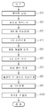
- 반도체 칩(6)의 영상을 획득하여 칩(6)의 불량 유무를 검사하는 반도체 칩 외관 검사 방법에 있어서,웨이퍼(5)를 로딩(S10)한 후, 각 칩(6)의 배열이 X-Y 스테이지(10)의 이송방향과 나란하도록 정렬하는 웨이퍼 정렬단계(S20)와,상기 웨이퍼 정렬단계(S20)를 거친 후, 웨이퍼(5)를 라인스캔 카메라(41)(Line scan camera)와 조명부(45)가 위치한 검사초기위치로 이동하는 웨이퍼 이동단계(S30)와,상기 웨이퍼 이동단계(S30)를 거친 후, 상기 조명부(45)를 온 시키고 상기 X-Y 스테이지(10)를 통해 웨이퍼(5)를 이동시키면서 웨이퍼(5)로부터 반사되는 빛을 라인스캔 카메라(41)로 스캔하는 1차 스캔단계(S40)와,상기 스캔단계를 거친 후, 상기 라인스캔 카메라(41)를 통해 스캔된 영상을 이용하여 각 칩(6)의 불량 유무를 분석하는 영상 분석단계(S70)와,상기 영상 분석단계(S70)를 거친 후, 불량 유무에 대한 분석결과를 맵데이터로 작성하는 불량칩 맵데이터 작성단계(S80)와,상기 불량칩 맵데이터 작성단계(S80)를 거친 후, 웨이퍼(5)의 기준위치를 삼고자 하는 복수개의 칩(6) 위에 마킹을 실시하는 칩 마킹단계(S90)를 포함하여 이루어진 것을 특징으로 하는 반도체 칩 외관 검사 방법.
- 제 1 항에 있어서,상기 1차 스캔단계(S40)와 영상 분석단계(S70)의 사이에는,상기 1차 스캔단계(S40)를 거친 후, 상기 조명부(45)의 광량을 1차 스캔단계(S40)시 보다 밝거나 또는 어둡게 재설정하는 광량 재설정 단계(S50)와, 상기 광량 재설정 단계(S50)를 거친 후, 상기 X-Y 스테이지(10)를 통해 웨이퍼(5)를 다시 이동시키면서 웨이퍼(5)로부터 반사되는 빛을 상기 라인스캔 카메라(41)로 다시 스캔하는 2차 스캔단계(S60)를 더 포함하는 것을 특징으로 하는 반도체 칩 외관 검사 방법.
- 제 1 항에 있어서,상기 웨이퍼 정렬단계(S20)는, 상기 X-Y 스테이지(10)의 상측에 설치된 회전 스테이지(20)에 상기 웨이퍼(5)가 붙착되어 있는 웨이퍼링(7)을 진공흡착으로 고정한 후, 에어리어 카메라(31)(Area camera)를 이용하여 웨이퍼(5)의 영상을 확인하면서 조이스틱을 통해 좌,우,전,후 및 회전시켜 각 칩(6)의 배열을 X-Y 스테이지(10)의 이송방향과 나란하도록 정렬하는 것을 특징으로 하는 반도체 칩 외관 검사 방법.
- 제 1 항에 있어서,상기 영상 분석단계(S70)는, 상기 라인스캔 카메라(41)를 통해 스캔된 영상의 그레이레벨 분포를 분석하여 불량칩에 해당되는 그레이레벨 분포를 갖는지 양품 칩에 해당되는 그레이레벨 분포를 갖는지 분석하여 칩(6)의 불량 유무를 판별하는 것을 특징으로 하는 반도체 칩 외관 검사 방법.
- 반도체 칩(6)의 영상을 획득하여 칩(6)의 불량 유무를 검사하는 반도체 칩 외관 검사 장치에 있어서,테이블(2)의 상측에 X-Y 방향으로 이동하도록 설치되는 X-Y 스테이지(10)와,상기 X-Y 스테이지(10)의 상측에 설치됨과 아울러 웨이퍼(5)가 부착되어 있는 웨이퍼링(7)을 고정하고 일정각도 회전시키는 회전 스테이지(20)와,상기 테이블(2)의 상측에 설치됨과 아울러 상기 웨이퍼(5)의 각 칩(6)의 배열을 정렬하기 위한 영상을 촬영하도록 에어리어 카메라(31)(Area camera)를 구비한 정렬부(30)와,상기 테이블(2)의 상측에서 정렬부(30)의 일측에 설치됨과 아울러 상기 웨이퍼(5)에 빛을 조사하는 조명부(45) 및 상기 웨이퍼(5)로부터 반사되는 빛을 스캔하는 라인스캔 카메라(41)(Line scan camera)를 구비한 스캔부(40)와,상기 조명부(45)의 광량을 제어하는 조명제어부와,상기 각 구성요소들을 제어함과 아울러 상기 라인스캔 카메라(41)를 통해 스캔된 영상을 이용하여 양품과 불량품을 판별하여 맵데이터를 작성하는 제어부를 포함하여 이루어진 것을 특징으로 하는 반도체 칩 외관 검사 장치.
- 제 5 항에 있어서,상기 라인스캔 카메라(41)는 상기 테이블(2)의 상측에 지지프레임(44)을 통해 일정높이에 설치되고, 상기 라인스캔 카메라(41)의 하부에는 고배율로 스캔할 수 있도록 하단에 렌즈(43)를 구비한 경통(42)이 설치되며,상기 조명부(45)는 상기 지지프레임(44)에 지지됨과 아울러 상기 렌즈(43)의 수직방향 하측으로 일정간격 이격되어 설치된 것을 특징으로 하는 반도체 칩 외관 검사 장치.
- 제 6 항에 있어서,상기 조명부(45)는,상기 지지프레임(44)에 지지되게 설치됨과 아울러 내부가 비어있는 하우징(46)과,상기 하우징(46)의 내부 일측에 설치되어 수평방향으로 빛을 조사하는 복수개의 LED(47)와,상기 하우징(46)의 내부 타측에 경사지게 설치되되 상기 렌즈(43)의 수직방향으로 동일선상에 위치하여 상기 LED(47)로부터 조사되는 빛을 상기 웨이퍼(5)측으로 반사시킴과 동시에 상기 웨이퍼(5)로부터 반사되는 빛이 자신을 통과되게 하는 하프미러(47)와,상기 하프미러(47)의 상,하측 방향과 대응하는 상기 하우징(46)의 상,하측면에 빛이 관통하도록 형성된 관통공(49)으로 이루어진 것을 특징으로 하는 반도체 칩 외관 검사 장치.
- 제 5 항에 있어서,상기 조명제어부는, 상기 라인스캔 카메라(41)를 이용하여 웨이퍼(5)를 1,2차에 걸쳐 스캔할 경우, 1차 스캔시의 조명부(45) 광량과 2차 스캔시의 조명부(45) 광량을 상이하게 설정하는 것을 특징으로 하는 반도체 칩 외관 검사 장치.
- 제 5 항에 있어서,상기 정렬부(30)에는 상기 라인스캔 카메라(41)를 통한 웨이퍼(5)의 전체 검사가 끝난 뒤 언로딩하기 전에 웨이퍼(5)의 기준위치를 설정하기 위해 복수개의 칩(6) 위에 잉크 마킹을 할 수 있도록 잉크마커(32)가 설치된 것을 특징으로 하는 반도체 칩 외관 검사 장치.
Priority Applications (1)
| Application Number | Priority Date | Filing Date | Title |
|---|---|---|---|
| KR1020080130404A KR101013573B1 (ko) | 2008-12-19 | 2008-12-19 | 반도체 칩 외관 검사 방법 및 그 장치 |
Applications Claiming Priority (1)
| Application Number | Priority Date | Filing Date | Title |
|---|---|---|---|
| KR1020080130404A KR101013573B1 (ko) | 2008-12-19 | 2008-12-19 | 반도체 칩 외관 검사 방법 및 그 장치 |
Publications (2)
| Publication Number | Publication Date |
|---|---|
| KR20100071621A true KR20100071621A (ko) | 2010-06-29 |
| KR101013573B1 KR101013573B1 (ko) | 2011-02-14 |
Family
ID=42369090
Family Applications (1)
| Application Number | Title | Priority Date | Filing Date |
|---|---|---|---|
| KR1020080130404A Expired - Fee Related KR101013573B1 (ko) | 2008-12-19 | 2008-12-19 | 반도체 칩 외관 검사 방법 및 그 장치 |
Country Status (1)
| Country | Link |
|---|---|
| KR (1) | KR101013573B1 (ko) |
Cited By (14)
| Publication number | Priority date | Publication date | Assignee | Title |
|---|---|---|---|---|
| KR101043236B1 (ko) * | 2010-11-17 | 2011-06-22 | 표준정보기술 주식회사 | Led 칩 외관 검사 장치 및 그 방법 |
| KR101462546B1 (ko) * | 2013-12-27 | 2014-11-17 | 주식회사 로보스타 | 엠엘씨씨칩 단면 검사장비 |
| KR20160066421A (ko) * | 2014-12-02 | 2016-06-10 | 세메스 주식회사 | 웨이퍼 검사 방법 |
| KR101667686B1 (ko) | 2016-06-29 | 2016-10-20 | 에스에스오트론 주식회사 | 반도체 패키지의 마킹 및 맵 형성 장치 |
| KR20170088285A (ko) * | 2016-01-22 | 2017-08-01 | 가부시기가이샤 디스코 | 웨이퍼의 가공 방법 |
| US10299210B2 (en) | 2015-01-21 | 2019-05-21 | Samsung Electronics Co., Ltd. | Method and apparatus for reducing power consumption of electronic device |
| CN111077155A (zh) * | 2018-10-18 | 2020-04-28 | 三星显示有限公司 | 显示面板检查系统和显示面板的检查方法 |
| CN111279181A (zh) * | 2017-10-25 | 2020-06-12 | 弗劳恩霍夫应用研究促进协会 | 用于对运动的构件进行光学监测的设备和方法 |
| CN113578790A (zh) * | 2021-08-02 | 2021-11-02 | 深圳瑞波光电子有限公司 | 一种芯片检测装置 |
| KR20220006180A (ko) * | 2020-07-08 | 2022-01-17 | 주식회사 라온옵틱스 | 행/열 인덱스 기반 led 웨이퍼 맵 생성 방법 및 시스템 |
| CN115078392A (zh) * | 2022-07-29 | 2022-09-20 | 深圳市泽信智能装备有限公司 | 一种半导体芯片缺陷检测设备及方法 |
| CN115954290A (zh) * | 2023-01-05 | 2023-04-11 | 华引芯(武汉)科技有限公司 | 一种芯片检测方法及其控制装置、存储介质 |
| CN117894720A (zh) * | 2024-03-15 | 2024-04-16 | 视睿(杭州)信息科技有限公司 | 半导体晶圆芯片分选方法及装置 |
| KR20240156176A (ko) * | 2023-04-21 | 2024-10-29 | 주식회사 넥사 | 웨이퍼 통합 검사 장치 |
Families Citing this family (3)
| Publication number | Priority date | Publication date | Assignee | Title |
|---|---|---|---|---|
| KR101192331B1 (ko) | 2012-08-23 | 2012-10-17 | 함상민 | 에어리어 카메라를 이용한 렌즈의 비전 검사장치 및 검사방법 |
| KR101407519B1 (ko) * | 2012-10-23 | 2014-06-13 | 한국기계연구원 | 캡슐형 가변축 복합 가공 장치의 스테이지 유닛 |
| KR102357695B1 (ko) * | 2020-08-03 | 2022-02-08 | (주) 인텍플러스 | 외관 검사 시스템 |
Family Cites Families (3)
| Publication number | Priority date | Publication date | Assignee | Title |
|---|---|---|---|---|
| JP2007234932A (ja) * | 2006-03-02 | 2007-09-13 | Olympus Corp | 外観検査装置 |
| JP2008180578A (ja) * | 2007-01-24 | 2008-08-07 | Toppan Printing Co Ltd | 周期性パターンのムラ検査装置 |
| KR100969283B1 (ko) * | 2007-05-16 | 2010-07-09 | 아주하이텍(주) | 광학 검사 장치 |
-
2008
- 2008-12-19 KR KR1020080130404A patent/KR101013573B1/ko not_active Expired - Fee Related
Cited By (17)
| Publication number | Priority date | Publication date | Assignee | Title |
|---|---|---|---|---|
| KR101043236B1 (ko) * | 2010-11-17 | 2011-06-22 | 표준정보기술 주식회사 | Led 칩 외관 검사 장치 및 그 방법 |
| KR101462546B1 (ko) * | 2013-12-27 | 2014-11-17 | 주식회사 로보스타 | 엠엘씨씨칩 단면 검사장비 |
| KR20160066421A (ko) * | 2014-12-02 | 2016-06-10 | 세메스 주식회사 | 웨이퍼 검사 방법 |
| US10299210B2 (en) | 2015-01-21 | 2019-05-21 | Samsung Electronics Co., Ltd. | Method and apparatus for reducing power consumption of electronic device |
| KR20170088285A (ko) * | 2016-01-22 | 2017-08-01 | 가부시기가이샤 디스코 | 웨이퍼의 가공 방법 |
| KR101667686B1 (ko) | 2016-06-29 | 2016-10-20 | 에스에스오트론 주식회사 | 반도체 패키지의 마킹 및 맵 형성 장치 |
| CN111279181A (zh) * | 2017-10-25 | 2020-06-12 | 弗劳恩霍夫应用研究促进协会 | 用于对运动的构件进行光学监测的设备和方法 |
| CN111279181B (zh) * | 2017-10-25 | 2023-10-03 | 弗劳恩霍夫应用研究促进协会 | 用于对运动的构件进行光学监测的设备和方法 |
| KR20200044252A (ko) * | 2018-10-18 | 2020-04-29 | 삼성디스플레이 주식회사 | 표시 패널 검사 시스템, 표시 패널 검사 방법 및 이를 이용한 표시 패널. |
| CN111077155A (zh) * | 2018-10-18 | 2020-04-28 | 三星显示有限公司 | 显示面板检查系统和显示面板的检查方法 |
| KR20220006180A (ko) * | 2020-07-08 | 2022-01-17 | 주식회사 라온옵틱스 | 행/열 인덱스 기반 led 웨이퍼 맵 생성 방법 및 시스템 |
| CN113578790A (zh) * | 2021-08-02 | 2021-11-02 | 深圳瑞波光电子有限公司 | 一种芯片检测装置 |
| CN115078392A (zh) * | 2022-07-29 | 2022-09-20 | 深圳市泽信智能装备有限公司 | 一种半导体芯片缺陷检测设备及方法 |
| CN115078392B (zh) * | 2022-07-29 | 2025-03-04 | 深圳市泽信智能装备有限公司 | 一种半导体芯片缺陷检测设备及方法 |
| CN115954290A (zh) * | 2023-01-05 | 2023-04-11 | 华引芯(武汉)科技有限公司 | 一种芯片检测方法及其控制装置、存储介质 |
| KR20240156176A (ko) * | 2023-04-21 | 2024-10-29 | 주식회사 넥사 | 웨이퍼 통합 검사 장치 |
| CN117894720A (zh) * | 2024-03-15 | 2024-04-16 | 视睿(杭州)信息科技有限公司 | 半导体晶圆芯片分选方法及装置 |
Also Published As
| Publication number | Publication date |
|---|---|
| KR101013573B1 (ko) | 2011-02-14 |
Similar Documents
| Publication | Publication Date | Title |
|---|---|---|
| KR101013573B1 (ko) | 반도체 칩 외관 검사 방법 및 그 장치 | |
| US7729528B2 (en) | Automated wafer defect inspection system and a process of performing such inspection | |
| CN101783306B (zh) | 检测晶片的系统和方法 | |
| CN101853797B (zh) | 用于检测晶片的系统和方法 | |
| CN104091766B (zh) | 检测晶片的系统和方法 | |
| KR101319682B1 (ko) | 전기 회로의 자동 수리 | |
| JP2008235892A (ja) | ウエハの縁部領域の欠陥の評価のための装置及び方法 | |
| JP2002014057A (ja) | 欠陥検査装置 | |
| KR101802843B1 (ko) | 자동 비전 검사 시스템 | |
| KR101514409B1 (ko) | 비전검사장치 | |
| JP2011158363A (ja) | Pga実装基板の半田付け検査装置 | |
| KR20220044741A (ko) | 웨이퍼 외관 검사 장치 및 방법 | |
| TWI502185B (zh) | 基板外觀自動檢測機 | |
| KR102764199B1 (ko) | 웨이퍼 외관 검사 장치 및 방법 | |
| KR100769691B1 (ko) | 탭 검사장치 및 이를 이용한 탭 검사방법 | |
| KR101030445B1 (ko) | Led 소자의 다이 및 와이어 본딩 검사 장치 및 그 방법 | |
| JP2002071576A (ja) | 外観検査装置および外観検査方法 | |
| KR20250148550A (ko) | 반도체 웨이퍼 검사 방법 및 반도체 웨이퍼 검사 장치 | |
| HK1201982B (en) | System and method for inspecting a wafer | |
| HK1149632B (en) | System and method for inspecting a wafer | |
| HK1165905A (en) | System and method for capturing illumination reflected in multiple directions |
Legal Events
| Date | Code | Title | Description |
|---|---|---|---|
| A201 | Request for examination | ||
| PA0109 | Patent application |
St.27 status event code: A-0-1-A10-A12-nap-PA0109 |
|
| PA0201 | Request for examination |
St.27 status event code: A-1-2-D10-D11-exm-PA0201 |
|
| PG1501 | Laying open of application |
St.27 status event code: A-1-1-Q10-Q12-nap-PG1501 |
|
| E902 | Notification of reason for refusal | ||
| PE0902 | Notice of grounds for rejection |
St.27 status event code: A-1-2-D10-D21-exm-PE0902 |
|
| E13-X000 | Pre-grant limitation requested |
St.27 status event code: A-2-3-E10-E13-lim-X000 |
|
| P11-X000 | Amendment of application requested |
St.27 status event code: A-2-2-P10-P11-nap-X000 |
|
| P13-X000 | Application amended |
St.27 status event code: A-2-2-P10-P13-nap-X000 |
|
| R18-X000 | Changes to party contact information recorded |
St.27 status event code: A-3-3-R10-R18-oth-X000 |
|
| E701 | Decision to grant or registration of patent right | ||
| PE0701 | Decision of registration |
St.27 status event code: A-1-2-D10-D22-exm-PE0701 |
|
| GRNT | Written decision to grant | ||
| PR0701 | Registration of establishment |
St.27 status event code: A-2-4-F10-F11-exm-PR0701 |
|
| PR1002 | Payment of registration fee |
St.27 status event code: A-2-2-U10-U11-oth-PR1002 Fee payment year number: 1 |
|
| PG1601 | Publication of registration |
St.27 status event code: A-4-4-Q10-Q13-nap-PG1601 |
|
| R18-X000 | Changes to party contact information recorded |
St.27 status event code: A-5-5-R10-R18-oth-X000 |
|
| LAPS | Lapse due to unpaid annual fee | ||
| PC1903 | Unpaid annual fee |
St.27 status event code: A-4-4-U10-U13-oth-PC1903 Not in force date: 20140201 Payment event data comment text: Termination Category : DEFAULT_OF_REGISTRATION_FEE |
|
| PC1903 | Unpaid annual fee |
St.27 status event code: N-4-6-H10-H13-oth-PC1903 Ip right cessation event data comment text: Termination Category : DEFAULT_OF_REGISTRATION_FEE Not in force date: 20140201 |
|
| R18-X000 | Changes to party contact information recorded |
St.27 status event code: A-5-5-R10-R18-oth-X000 |
|
| PN2301 | Change of applicant |
St.27 status event code: A-5-5-R10-R13-asn-PN2301 St.27 status event code: A-5-5-R10-R11-asn-PN2301 |
|
| P22-X000 | Classification modified |
St.27 status event code: A-4-4-P10-P22-nap-X000 |
|
| R18-X000 | Changes to party contact information recorded |
St.27 status event code: A-5-5-R10-R18-oth-X000 |
|
| R18-X000 | Changes to party contact information recorded |
St.27 status event code: A-5-5-R10-R18-oth-X000 |
|
| P22-X000 | Classification modified |
St.27 status event code: A-4-4-P10-P22-nap-X000 |