KR20090106743A - Manufacturing method of semiconductor device - Google Patents
Manufacturing method of semiconductor device Download PDFInfo
- Publication number
- KR20090106743A KR20090106743A KR1020080032064A KR20080032064A KR20090106743A KR 20090106743 A KR20090106743 A KR 20090106743A KR 1020080032064 A KR1020080032064 A KR 1020080032064A KR 20080032064 A KR20080032064 A KR 20080032064A KR 20090106743 A KR20090106743 A KR 20090106743A
- Authority
- KR
- South Korea
- Prior art keywords
- film
- metal film
- forming
- preliminary
- preliminary metal
- Prior art date
- Legal status (The legal status is an assumption and is not a legal conclusion. Google has not performed a legal analysis and makes no representation as to the accuracy of the status listed.)
- Withdrawn
Links
Images


Classifications
-
- H—ELECTRICITY
- H10—SEMICONDUCTOR DEVICES; ELECTRIC SOLID-STATE DEVICES NOT OTHERWISE PROVIDED FOR
- H10P—GENERIC PROCESSES OR APPARATUS FOR THE MANUFACTURE OR TREATMENT OF DEVICES COVERED BY CLASS H10
- H10P95/00—Generic processes or apparatus for manufacture or treatments not covered by the other groups of this subclass
- H10P95/06—Planarisation of inorganic insulating materials
- H10P95/062—Planarisation of inorganic insulating materials involving a dielectric removal step
-
- H—ELECTRICITY
- H10—SEMICONDUCTOR DEVICES; ELECTRIC SOLID-STATE DEVICES NOT OTHERWISE PROVIDED FOR
- H10P—GENERIC PROCESSES OR APPARATUS FOR THE MANUFACTURE OR TREATMENT OF DEVICES COVERED BY CLASS H10
- H10P14/00—Formation of materials, e.g. in the shape of layers or pillars
- H10P14/60—Formation of materials, e.g. in the shape of layers or pillars of insulating materials
- H10P14/63—Formation of materials, e.g. in the shape of layers or pillars of insulating materials characterised by the formation processes
- H10P14/6302—Non-deposition formation processes
- H10P14/6304—Formation by oxidation, e.g. oxidation of the substrate
- H10P14/6314—Formation by oxidation, e.g. oxidation of the substrate of a metallic layer
-
- H—ELECTRICITY
- H10—SEMICONDUCTOR DEVICES; ELECTRIC SOLID-STATE DEVICES NOT OTHERWISE PROVIDED FOR
- H10P—GENERIC PROCESSES OR APPARATUS FOR THE MANUFACTURE OR TREATMENT OF DEVICES COVERED BY CLASS H10
- H10P50/00—Etching of wafers, substrates or parts of devices
- H10P50/60—Wet etching
- H10P50/66—Wet etching of conductive or resistive materials
- H10P50/663—Wet etching of conductive or resistive materials by chemical means only
- H10P50/667—Wet etching of conductive or resistive materials by chemical means only by liquid etching only
Landscapes
- Mechanical Treatment Of Semiconductor (AREA)
- Internal Circuitry In Semiconductor Integrated Circuit Devices (AREA)
Abstract
반도체 소자의 제조방법이 개시되어 있다. 반도체 소자의 제조방법은, 반도체 기판 상부에 제1 예비금속막을 형성하는 단계와, 제1 스텝커버리지를 갖는 제1 예비금속막을 식각하여 제1 스텝커버리지 보다 작은 제2 스텝커버리지를 갖는 제2 예비금속막을 형성하는 단계와, 제2 예비금속막의 표면을 산화하여 제3 예비금속막을 형성하는 단계와, 제3 예비금속막 상에 형성된 산화막을 연마하여 평탄한 금속막을 형성하는 단계를 포함한다. 이로써, 본 발명에 따른 큰 스텝커버리지를 갖는 금속막의 표면을 산화막을 이용하여 안정적으로 연마해줌으로써, 금속막의 표면의 스텝커버리지를 감소 및 쉽게 연마할 수 있는 효과가 있다. A method for manufacturing a semiconductor device is disclosed. A method of manufacturing a semiconductor device includes forming a first preliminary metal film on a semiconductor substrate, etching the first preliminary metal film having a first step coverage, and a second preliminary metal having a second step coverage smaller than the first step coverage. Forming a film, oxidizing the surface of the second premetal film to form a third premetal film, and polishing an oxide film formed on the third premetal film to form a flat metal film. Thus, by stably polishing the surface of the metal film having a large step coverage according to the present invention using an oxide film, there is an effect that can reduce and easily polish the step coverage of the surface of the metal film.
Description
본 발명은 반도체 소자의 제조방법에 관한 것이다.The present invention relates to a method for manufacturing a semiconductor device.
반도체를 제조하기 위한 여러 공정 중 웨이퍼 상에 형성된 박막의 평탄화 및 불필요한 박막의 제거를 위해 웨이퍼에 대한 연마 가공을 수행하는 공정을 웨이퍼 연마 공정이라 한다. Among various processes for manufacturing a semiconductor, a process of performing a polishing process on a wafer to planarize a thin film formed on a wafer and to remove unnecessary thin films is called a wafer polishing process.
웨이퍼 연마 공정은 소형 경량화를 지향하는 최근의 반도체 추세에서 매우 중요하게 인식되고 있는 공정 중 하나로서, 최근에는 슬러리(Slurry)와 같은 화학 연마제와 기계적 연마 장치를 적절히 조합 사용하여 연마를 진행하는 화학적 기계적 연마 방법이 주로 사용되고 있다.The wafer polishing process is one of the most important processes in the recent semiconductor trend toward miniaturization and light weight, and recently, the chemical mechanical process that performs polishing using a suitable combination of a chemical polishing agent such as slurry and a mechanical polishing device is performed. Polishing methods are mainly used.
상기 화학적 기계적 연마 방법은 웨이퍼 상에 형성된 박막의 재질이 텅스텐, 구리, 알루미늄 등 금속 재질로 형성된 금속막일 경우에 많이 사용되는데, 예를 들어, 웨이퍼 상에 형성되어 있는 절연층에 그 절연층을 관통하는 비아(Via), 비트라인 등의 도전층을 형성할 경우, 그것들을 형성하고 남은 절연층 표면의 불필요한 금속막은 화학적 기계적 연마 방법을 통해 제거하게 된다.The chemical mechanical polishing method is often used when the material of the thin film formed on the wafer is a metal film formed of a metal material such as tungsten, copper, aluminum, for example, penetrates the insulating layer through the insulating layer formed on the wafer. In the case of forming conductive layers such as vias and bit lines, unnecessary metal films on the surface of the insulating layer remaining after the formation of the vias and bit lines are removed by chemical mechanical polishing.
종래의 금속막에 대한 화학적 기계적 연마 방법은 화학 연마제와 기계적 연 마 장치를 사용하여 웨이퍼 표면에 형성된 금속막의 제거 및 평탄화를 진행하는 화학적 기계적 연마 단계로만 이루어져 있었는데, 이는 박막이 균일하게 형성되는 등의 장점을 가진 반면 슬러리와 같은 고가의 화학 연마제가 많이 소모되고 공정의 진행시간이 길게 소요되어 직접적인 생산비용의 증가와 더불어 제품 생산의 소요시간이 증가한다는 단점을 가지고 있다.Conventional chemical mechanical polishing methods for metal films consisted only of chemical mechanical polishing steps that proceed with the removal and planarization of the metal film formed on the wafer surface using a chemical abrasive and a mechanical polishing device. On the other hand, it consumes a lot of expensive chemical abrasives such as slurry and takes a long time to process, which leads to an increase in direct production cost and an increase in production time.
화학적 기계적 연마 방법과 더불어 금속막을 제거할 수 있는 방법으로는 웨이퍼를 식각용 화학 용액에 노출시킴으로써 금속막을 식각하는 습식 식각 방법을 생각해 볼 수 있는데, 이는 그 비용이 저렴하고 공정의 진행 시간이 짧게 소요된다는 장점이 있으나 식각을 통해 형성되는 박막 경계면이 불균일하게 형성되고 또한 공정을 끝내는 시점인 엔드 포인트(End point)의 제어가 쉽지 않다는 단점을 가지고 있다.In addition to the chemical mechanical polishing method, a method of removing a metal film may be a wet etching method of etching a metal film by exposing a wafer to an etching chemical solution, which is inexpensive and requires a short process time. However, there is a disadvantage in that the thin film interface formed through etching is unevenly formed and control of the end point, which is the end point of the process, is not easy.
본 발명은 공정 진행에 소요되는 시간을 단축시키고, 고가인 화학 연마제의 소모량을 감소시킬 수 있도록 하여 제품생산에 있어서의 생산비용 절감 및 전체 생산시간의 단축을 가져올 수 있는 반도체 소자의 제조방법을 제공한다. The present invention provides a method of manufacturing a semiconductor device that can shorten the time required to proceed the process, and can reduce the consumption of expensive chemical abrasives, thereby reducing the production cost and shortening the overall production time in the production of the product. do.
본 발명의 일 실시예에 따른 반도체 소자의 제조방법은, 반도체 기판 상부에 제1 예비금속막을 형성하는 단계와, 제1 스텝커버리지를 갖는 상기 제1 예비금속막을 식각하여 상기 제1 스텝커버리지 보다 작은 제2 스텝커버리지를 갖는 제2 예비 금속막을 형성하는 단계와, 상기 제2 예비금속막의 표면을 산화하여 제3 예비금속막을 형성하는 단계와, 상기 제3 예비금속막 상에 형성된 산화막을 연마하여 평탄한 금속막을 형성하는 단계를 포함한다. A method of manufacturing a semiconductor device according to an embodiment of the present invention may include forming a first preliminary metal film on a semiconductor substrate, and etching the first preliminary metal film having a first step coverage to be smaller than the first step coverage. Forming a second preliminary metal film having a second step coverage, oxidizing a surface of the second premetal film to form a third premetal film, and polishing an oxide film formed on the third premetal film Forming a metal film.
여기서, 상기 제1 예비금속막을 형성하는 단계 이전에, 상기 반도체 기판 상에 절연막을 형성하는 단계와, 상기 절연막 상에 베리어막을 형성하는 단계를 더 포함한다. Here, before the forming of the first preliminary metal layer, the method may further include forming an insulating film on the semiconductor substrate and forming a barrier film on the insulating film.
상기 평탄한 상기 금속막을 형성하는 단계 이후에, 상기 금속막 상에 하드마스크막을 형성하는 단계와, 상기 하드마스크막의 일부로 정의된 비트라인 형성 영역을 노출하는 마스크 패턴을 형성하는 단계와, 상기 하드마스크막, 상기 금속막 및 상기 베리어막을 상기 마스크 패턴을 식각마스크로서 이용하여 패터닝하는 단계를 더 포함한다. After forming the planar metal layer, forming a hard mask layer on the metal layer, forming a mask pattern exposing a bit line forming region defined as part of the hard mask layer, and forming the hard mask layer; The method may further include patterning the metal layer and the barrier layer using the mask pattern as an etching mask.
상기 제1 예비금속막을 형성하는 단계에서 상기 제1 예비금속막은 텅스텐막이다. In the forming of the first preliminary metal film, the first preliminary metal film is a tungsten film.
상기 제2 예비금속막을 형성하는 단계에서, 상기 제1 예비금속막은 습식 에천트에 의하여 식각된다. In the forming of the second preliminary metal film, the first premetal film is etched by a wet etchant.
상기 습식 에천트는 스프레이(spray) 방식으로 제공된다. The wet etchant is provided by spraying.
상기 습식 에천트는 H2O2를 포함하는 H2O2용액, HF를 포함하는 HF용액, HNO3을 포함하는 HNO3용액, H2SO4, H2O2 및 H2O을 포함하는 SPM용액, NH4OH, H2O2 및 H2O을 포함하는 SC-1용액, HCl, H2O2 및 H2O을 포함하는 SC-2용액 및 H2O2와 HF를 혼합한 혼 합용액 중 어느 하나를 포함한다. SPM containing H 2 O 2 solution containing the wet etchant H 2 O 2, HNO 3 solution, H 2 SO 4, H 2 O 2 and H 2 O containing HF solution, HNO 3 containing HF Solution, SC-1 solution containing NH 4 OH, H 2 O 2 and H 2 O, SC-2 solution containing HCl, H 2 O 2 and H 2 O and a mixture of H 2 O 2 and HF It contains any one of the solution.
상기 제3 예비금속막을 형성하는 단계에서, 상기 제2 예비금속막은 오존을 포함하는 순수(O3 DI water)에 의하여 산화된다. In the forming of the third preliminary metal film, the second premetal film is oxidized by pure water (O 3 DI water) containing ozone.
상기 평탄한 상기 금속막을 형성하는 단계에서, 상기 산화막은 화학적 기계적 연마(Chemical mechanical polishing) 공정에 의하여 연마된다. In the forming of the flat metal film, the oxide film is polished by a chemical mechanical polishing process.
본 발명의 다른 실시예에 따른 반도체 소자의 제조방법은, 반도체 기판 상부에 제1 예비금속막을 형성하는 단계와, 제1 사이즈를 갖는 제1 요철부를 갖는 상기 제1 예비금속막을 식각하여 상기 제1 요철부 보다 작은 제2 사이즈를 갖는 제2 요철부를 갖는 제2 예비금속막을 형성하는 단계와, 상기 제2 예비금속막의 표면을 산화하여 제3 예비금속막을 형성하는 단계와, 상기 제3 예비금속막 상에 형성된 산화막을 연마하여 평탄한 금속막을 형성하는 단계를 포함한다. According to another aspect of the present invention, there is provided a method of manufacturing a semiconductor device, including forming a first preliminary metal film on a semiconductor substrate, etching the first preliminary metal film having a first uneven portion having a first size, and etching the first preliminary metal film. Forming a second premetal film having a second uneven portion having a second size smaller than the uneven portion, oxidizing the surface of the second premetal film to form a third premetal film, and the third premetal film Polishing the oxide film formed on the substrate to form a flat metal film.
상기 제1 예비금속막을 형성하는 단계 이전에, 상기 반도체 기판 상에 절연막을 형성하는 단계와, 상기 절연막 상에 베리어막을 형성하는 단계를 더 포함한다. Prior to forming the first preliminary metal film, the method may further include forming an insulating film on the semiconductor substrate and forming a barrier film on the insulating film.
상기 평탄한 상기 금속막을 형성하는 단계 이후에, 상기 금속막 상에 하드마스크막을 형성하는 단계와, 상기 하드마스크막의 일부로 정의된 비트라인 형성 영역을 노출하는 마스크 패턴을 형성하는 단계와, 상기 하드마스크막, 상기 금속막 및 상기 베리어막을 상기 마스크 패턴을 식각마스크로서 이용하여 패터닝하는 단계를 더 포함한다. After forming the planar metal layer, forming a hard mask layer on the metal layer, forming a mask pattern exposing a bit line forming region defined as part of the hard mask layer, and forming the hard mask layer; The method may further include patterning the metal layer and the barrier layer using the mask pattern as an etching mask.
상기 제1 예비금속막을 형성하는 단계에서 상기 제1 예비금속막은 텅스텐막이다. In the forming of the first preliminary metal film, the first preliminary metal film is a tungsten film.
상기 제2 예비금속막을 형성하는 단계에서, 상기 제1 예비금속막은 습식 에천트에 의하여 식각된다. In the forming of the second preliminary metal film, the first premetal film is etched by a wet etchant.
상기 습식 에천트는 스프레이(spray) 방식으로 제공된다. The wet etchant is provided by spraying.
상기 습식 에천트는 H2O2를 포함하는 H2O2용액, HF를 포함하는 HF용액, HNO3을 포함하는 HNO3용액, H2SO4, H2O2 및 H2O을 포함하는 SPM용액, NH4OH, H2O2 및 H2O을 포함하는 SC-1용액, HCl, H2O2 및 H2O을 포함하는 SC-2용액 및 H2O2와 HF를 혼합한 혼합용액 중 어느 하나를 포함한다. SPM containing H 2 O 2 solution containing the wet etchant H 2 O 2, HNO 3 solution, H 2 SO 4, H 2 O 2 and H 2 O containing HF solution, HNO 3 containing HF Solution, SC-1 solution containing NH 4 OH, H 2 O 2 and H 2 O, SC-2 solution containing HCl, H 2 O 2 and H 2 O and a mixture of H 2 O 2 and HF mixed Any one of the solutions.
상기 제3 예비금속막을 형성하는 단계에서, 상기 제2 예비금속막은 오존을 포함하는 순수(O3 DI water)에 의하여 산화된다. In the forming of the third preliminary metal film, the second premetal film is oxidized by pure water (O 3 DI water) containing ozone.
상기 평탄한 상기 금속막을 형성하는 단계에서, 상기 산화막은 화학적 기계적 연마(Chemical mechanical polishing) 공정에 의하여 연마된다.In the forming of the flat metal film, the oxide film is polished by a chemical mechanical polishing process.
본 발명은 금속막을 평탄화하기 위한 연마 공정을 수행하기 전에 습식 식각 공정 및 세정 공정을 인-시튜(In-Situ) 방식으로 수행하여 상기 금속막의 표면에 산화막을 형성시킨 후, 상기 산화막을 이용하여 상기 금속막의 표면을 안정적으로 연마한다. According to the present invention, a wet etching process and a cleaning process are performed in an in-situ manner to form an oxide film on the surface of the metal film before the polishing process for flattening the metal film. The surface of the metal film is polished stably.
이렇게 하면, 상기 금속막 표면의 거칠기를 감소시킬 수 있을 뿐만 아니라, 상기 연마 공정 중 상기 산화막에 의하여 공정 진행에 소요되는 시간을 단축시킬 수 있으며, 고가인 화학 연마제의 소모량을 감소시킬 수 있다. In this way, not only the roughness of the surface of the metal film can be reduced, but also the time required for the process progress by the oxide film during the polishing process can be shortened, and the consumption of expensive chemical abrasives can be reduced.
그 결과, 제품생산에 있어서의 생산비용 및 전체 생산시간을 단축시킬 수 있다. As a result, it is possible to shorten the production cost and overall production time in the production of the product.
이하, 첨부된 도면을 참조하여 본 발명의 바람직한 실시예를 상세하게 설명하도록 한다. Hereinafter, exemplary embodiments of the present invention will be described in detail with reference to the accompanying drawings.
본 발명에서 빈번하게 사용되는 용어인 스텝커버리지는, 예를 들어, 금속막의 표면으로부터 돌출된 철부와 오목하게 들어간 요부들에 대해 경사진 단차비를 말한다. Step coverage, which is a term frequently used in the present invention, refers to a stepped ratio that is inclined, for example, with respect to convex portions projecting from the surface of the metal film and concave portions.
도 1 내지 도 7들은 본 발명의 실시예에 따른 반도체 소자의 제조방법을 설명하기 위한 공정별 단면도들이다. 1 to 7 are cross-sectional views of processes for describing a method of manufacturing a semiconductor device according to an embodiment of the present invention.
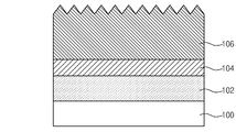
도 1은 반도체 기판 상부에 제1 예비금속막을 형성한 단면도이다. 1 is a cross-sectional view of forming a first preliminary metal film on a semiconductor substrate.
도 1을 참조하면, 반도체 기판(100) 상에는 절연막(102)이 형성되며, 상기 절연막(102)은, 예를 들어, 산화막일 수 있다. Referring to FIG. 1, an
상기 절연막(102) 상에는 베리어막(104) 및 제1 예비금속막(106)이 형성된다. 상기 베리어막(104)은, 예를 들어, 텅스텐질화막일 수 있으며, 상기 제1 예비금속막(106)은, 예를 들어, 제1 스텝커버리지를 갖는 텅스텐막일 수 있다. The
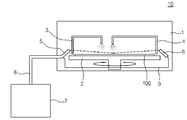
도 2는 본 발명에 따른 반도체 소자의 제조방법에서의 평탄화가 수행되는 연마 장비에 포함된 세정 장비를 나타낸 도면이다. 2 is a view showing the cleaning equipment included in the polishing equipment is performed planarization in the method of manufacturing a semiconductor device according to the present invention.
도 2를 참조하면, 본 발명의 실시예에 따른 세정 장비(10)는 챔버(1), 제1 습식 에천트 제공부(3), 제2 습식 에천트 제공부(4), 제1 오존-순수 제공부(5), 제2 오존-순수 제공부(6) 및 오존-순수 공급부(7)를 포함한다. 2, the
상기 챔버(1) 내에는 로딩부(2)가 배치되며, 상기 로딩부(2) 상에는 반도체 기판(100)이 배치된다. 상기 로딩부(2)는 상기 반도체 기판(100)을 로딩하고 수용한다. The
상기 챔버(1)는 상기 제1 및 제2 습식 에천트 제공부(3, 4)들로부터 제공된 습식 에천트들이 상기 반도체 기판(100)에 형성된 박막들과 반응하기에 적합한 공정 환경을 제공한다. The
여기서, 상기 습식 에천트는, 예를 들어, H2O2를 포함하는 H2O2용액, HF를 포함하는 HF용액, HNO3을 포함하는 HNO3용액, H2SO4, H2O2 및 H2O을 포함하는 SPM용액, NH4OH, H2O2 및 H2O을 포함하는 SC-1용액, HCl, H2O2 및 H2O을 포함하는 SC-2용액 및 H2O2와 HF를 혼합한 혼합용액 중 어느 하나일 수 있으며, 상기 습식 에천트는, 예를 들어, 상기 반도체 기판(100) 상에 스프레이(spray) 방식으로 제공될 수 있다. Here, the wet etchant, for example, H 2 O 2 solution containing H 2 O 2 , HF solution containing HF, HNO 3 solution containing HNO 3 , H 2 SO 4 , H 2 O 2 And SPM solution containing H 2 O, NH 4 OH, H 2 O 2 and SC-1 solution containing H 2 O, HCl, H 2 O 2 and the SC-2 solution and H 2 O containing H 2 O It may be any one of a mixed solution of 2 and HF, the wet etchant, for example, may be provided on the
한편, 상기 제1 및 제2 습식 에천트 제공부(3, 4)들은 상기 반도체 기판(100)에 형성된 박막들과 상기 습식 에천트가 반응하도록 상기 챔버(1)에 상기 습식 에천트를 공급하는 습식 에천트 공급부(도시안됨)와 연결되며, 상기 습식 에천트 공급부는 상기 챔버(1)의 외부에 배치될 수 있다. Meanwhile, the first and second wet
계속해서, 상기 제1 및 제2 오존-순수 제공부(5, 6)들은 상기 챔버(1)에 오 존을 포함하는 순수를 공급하는 오존-순수 공급부(7)와 연결되며, 상기 오존-순수 공급부(7)는 상기 챔버(1)의 외부에 배치된다. Subsequently, the first and second ozone-pure
상기 제1 및 제2 오존-순수 제공부(5, 6)들에는 상기 오존을 포함하는 순수를 공급하기 위한 제1배관(8) 및 제2배관(9)이 연결된다. The first and second ozone-pure
본 실시예에 따른, 상기 세정 장비를 이용하여 상기 반도체 기판(100)에 형성된 박막들의 표면에 후술될 산화막을 형성시킨 후, 상기 산화막을 이용하여 상기 반도체 기판(100)에 형성된 박막들의 스텝커버리지를 낮춘다. After forming the oxide film to be described later on the surface of the thin film formed on the
이렇게 하면, 후속 연마 공정에서 공정 진행에 소요되는 시간을 단축시킬 수 있을 뿐만 아니라 고가인 화학 연마제의 소모량을 감소시킬 수 있다. This not only shortens the time required for the process in the subsequent polishing process but also reduces the consumption of expensive chemical abrasives.
또한, 상기 반도체 기판(100)에 형성된 박막들의 표면을 상기 산화막을 이용하여 안정적으로 연마해줄 수 있어, 그 결과, 균일한 막을 형성할 수 있다. In addition, the surfaces of the thin films formed on the
도 3은 도 2에 도시된 세정 장비를 이용하여 제1 예비금속막을 식각하여 제2 예비금속막을 형성한 단면도이다. FIG. 3 is a cross-sectional view of a second preliminary metal film formed by etching the first preliminary metal film by using the cleaning equipment illustrated in FIG. 2.
도 3을 참조하면, 상기 베리어막(104) 상에 제1 예비금속막(106)이 형성된 후, 상기 제1 예비금속막(106)은 도 2에 도시된 세정 장비(10)을 이용하여 식각된다. Referring to FIG. 3, after the first
상기 제1 예비금속막(106a)은, 예를 들어, 상기 제1 및 제2 습식 에천트 제공부(3, 4)들로부터 제공된 상기 습식 에천트에 의하여 식각된다.The first
이 결과, 상기 베리어막(104) 상에는 상기 제1 스텝커버리지 보다 작은 제2 스텝커버리지를 갖는 제2 예비금속막(106a)이 형성된다. As a result, a second
도 4는 도 3의 제2 예비금속막의 표면을 산화하여 산화막을 갖는 제3 예비금속막을 형성한 단면도이다. 4 is a cross-sectional view of a third premetal film having an oxide film formed by oxidizing the surface of the second premetal film of FIG. 3.
도 4를 참조하면, 상기 베리어막(104) 상에 제2 예비금속막(106a)이 형성된 후, 상기 제2 예비금속막(106a)의 표면은, 예를 들어, 오존을 포함하는 순수(O3 DI water)에 의하여 산화되어, 상기 베리어막(104) 상에는 제3 예비금속막(106b)이 형성된다. Referring to FIG. 4, after the second
이때, 상기 제2 예비금속막(106a)의 표면은 상기 오존을 포함하는 순수에 의하여 산화하여 상기 제3 예비금속막(106b) 상에는 산화막(106c)이 형성된다. In this case, the surface of the second
도 5는 산화막을 갖는 제3 예비금속막 상에 형성된 산화막을 연마하여 금속막을 형성한 단면도이다. 5 is a cross-sectional view of a metal film formed by polishing an oxide film formed on a third preliminary metal film having an oxide film.
도 5를 참조하면, 상기 베리어막(104) 상에 상기 산화막(106c)을 갖는 제3 예비금속막(106b)이 형성된 후, 상기 산화막(106c)은, 예를 들어, 화학적 기계적 연마(Chemical mechanical polishing) 공정에 의하여 연마되어 상기 제3 예비금속막(106b)으로부터 제거된다. Referring to FIG. 5, after the third
이로써, 상기 베리어막(104) 상에는 평탄면을 갖는 금속막(106d)이 형성된다. As a result, a
본 실시예에 의하면, 큰 스텝커버리지를 갖는 금속막을 평탄화하기 위한 연마 공정을 수행하기 전에 습식 식각 공정 및 세정 공정을 인-시튜(In-Situ) 방식으로 수행하여 상기 금속막의 표면의 스텝커버리지를 감소 및 쉽게 연마되는 산화막 을 형성한 후, 상기 산화막 및 상기 금속막을 연마하여 상기 금속막의 표면의 거칠기를 감소시킬 수 있다. According to this embodiment, before performing the polishing process for planarizing the metal film having a large step coverage, the wet etching process and the cleaning process are performed in an in-situ manner to reduce the step coverage of the surface of the metal film. And after forming the easily polished oxide film, the oxide film and the metal film may be polished to reduce the roughness of the surface of the metal film.
또한, 상기 연마 공정 중 상기 산화막에 의하여 공정 진행에 소요되는 시간을 단축시킬 수 있으며, 고가인 화학 연마제의 소모량을 감소시킬 수 있다. In addition, it is possible to shorten the time required to proceed the process by the oxide film during the polishing process, it is possible to reduce the consumption of expensive chemical abrasives.
도 6은 도 5의 금속막 상에 하드마스크막 및 마스크 패턴을 형성한 단면도이다. 6 is a cross-sectional view of a hard mask film and a mask pattern formed on the metal film of FIG. 5.
도 6을 참조하면, 상기 베리어막(104) 상에 평탄면을 갖는 금속막(106d)이 형성된 후, 상기 평탄면을 갖는 금속막(106d) 상에는 하드마스크막(108)이 형성된다. 상기 하드마스크막(108)은, 예를 들어, 질화막일 수 있다. Referring to FIG. 6, after the
상기 하드마스크막(108) 상에는 비트라인 형성 영역을 노출하는 마스크 패턴(110)이 형성된다. The
도 7은 마스크 패턴을 식각마스크로서 이용하여 하드마스크막의 하부 박막들을 패터닝한 단면도이다. 7 is a cross-sectional view of patterning lower layers of a hard mask layer using a mask pattern as an etching mask.
도 7을 참조하면, 상기 하드마스크막(108) 상에 마스크 패턴(110)이 형성된 후, 상기 하드마스크막(108), 상기 금속막(106d) 및 상기 베리어막(104)은 상기 마스크 패턴(110)을 식각마스크로서 이용하여 식각되어, 상기 절연막(102) 상에는 베리어막 패턴(104a), 금속막 패턴(106e) 및 하드마스크막 패턴(108a)으로 이루어진 비트라인(BL)이 형성된다. Referring to FIG. 7, after the
이와 다르게, 본 발명의 다른 실시예에 따른 반도체 소자의 제조방법에서 명명된 제1 및 제2 사이즈들을 갖는 제1 및 제2 요철부들은 상기 본 발명의 일 실시 예에 따른 반도체 소자의 제조방법에서 명명된 제1 및 제2 스텝커버리지들과 실질적으로 동일한 역할을 한다.Alternatively, the first and second uneven portions having the first and second sizes named in the method of manufacturing a semiconductor device according to another embodiment of the present invention may be used in the method of manufacturing a semiconductor device according to an embodiment of the present invention. It serves substantially the same as the named first and second step coverages.
한편, 제1 사이즈를 갖는 제1 요철부를 갖는 제1 예비금속막을 형성한 후, 상기 제1 요철부를 갖는 상기 제1 예비금속막을 식각하여 상기 제1 요철부 보다 작은 제2 사이즈를 갖는 제2 요철부를 갖는 제2 예비금속막을 형성한다. 그런 다음, 상기 제2 예비금속막의 표면을 산화하여 제3 예비금속막을 형성한다. Meanwhile, after the first preliminary metal film having the first uneven portion having the first size is formed, the first premetal film having the first uneven portion is etched to form the second unevenness having a second size smaller than the first uneven portion. A second preliminary metal film having a portion is formed. Then, the surface of the second premetal film is oxidized to form a third premetal film.
계속해서, 상기 제3 예비금속막 상에 형성된 산화막을 연마하여 평탄한 금속막을 형성한다. Subsequently, the oxide film formed on the third preliminary metal film is polished to form a flat metal film.
이렇게 하면, 큰 사이즈를 갖는 요철부를 갖는 금속막을 산화막을 이용하여 안정적으로 연마해줌으로써, 금속막의 표면의 요철부를 감소 및 쉽게 연마할 수 있으며, 그 결과, 실질적으로 동일한 본 발명의 효과를 얻을 수 있다. In this way, by stably polishing the metal film having the concave-convex portion having a large size by using the oxide film, the concave-convex portion on the surface of the metal film can be reduced and easily polished, and as a result, the effect of the present invention that is substantially the same can be obtained. .
이후, 일련의 후속 공정들을 차례로 수행하여 본 발명의 실시예에 따른 반도체 소자를 완성한다.Thereafter, a series of subsequent processes are performed in sequence to complete the semiconductor device according to the embodiment of the present invention.
이상, 여기에서는 본 발명을 특정 실시예에 관련하여 도시하고 설명하였지만, 본 발명이 그에 한정되는 것은 아니며, 이하의 특허청구의 범위는 본 발명의 정신과 분야를 이탈하지 않는 한도 내에서 본 발명이 다양하게 개조 및 변형될 수 있다는 것을 당업계에서 통상의 지식을 가진 자가 용이하게 알 수 있다. As mentioned above, although the present invention has been illustrated and described with reference to specific embodiments, the present invention is not limited thereto, and the following claims are not limited to the scope of the present invention without departing from the spirit and scope of the present invention. It can be easily understood by those skilled in the art that can be modified and modified.
도 1은 반도체 기판 상부에 제1 예비금속막을 형성한 단면도이다. 1 is a cross-sectional view of forming a first preliminary metal film on a semiconductor substrate.
도 2는 본 발명에 따른 반도체 소자의 제조방법에서의 평탄화가 수행되는 연마 장비에 포함된 세정 장비를 나타낸 도면이다. 2 is a view showing the cleaning equipment included in the polishing equipment is performed planarization in the method of manufacturing a semiconductor device according to the present invention.
도 3은 도 2에 도시된 연마 장비를 이용하여 제1 예비금속막을 식각하여 제2 예비금속막을 형성한 단면도이다. FIG. 3 is a cross-sectional view of a second preliminary metal film formed by etching the first preliminary metal film using the polishing apparatus illustrated in FIG. 2.
도 4는 도 3의 제2 예비금속막의 표면을 산화하여 산화막을 갖는 제3 예비금속막을 형성한 단면도이다. 4 is a cross-sectional view of a third premetal film having an oxide film formed by oxidizing the surface of the second premetal film of FIG. 3.
도 5는 산화막을 갖는 제3 예비금속막 상에 형성된 산화막을 연마하여 금속막을 형성한 단면도이다. 5 is a cross-sectional view of a metal film formed by polishing an oxide film formed on a third preliminary metal film having an oxide film.
도 6은 도 5의 금속막 상에 하드마스크막 및 마스크 패턴을 형성한 단면도이다. 6 is a cross-sectional view of a hard mask film and a mask pattern formed on the metal film of FIG. 5.
도 7은 마스크 패턴을 식각마스크로서 이용하여 하드마스크막의 하부 박막들을 패터닝한 단면도이다. 7 is a cross-sectional view of patterning lower layers of a hard mask layer using a mask pattern as an etching mask.
Claims (18)
Priority Applications (1)
| Application Number | Priority Date | Filing Date | Title |
|---|---|---|---|
| KR1020080032064A KR20090106743A (en) | 2008-04-07 | 2008-04-07 | Manufacturing method of semiconductor device |
Applications Claiming Priority (1)
| Application Number | Priority Date | Filing Date | Title |
|---|---|---|---|
| KR1020080032064A KR20090106743A (en) | 2008-04-07 | 2008-04-07 | Manufacturing method of semiconductor device |
Publications (1)
| Publication Number | Publication Date |
|---|---|
| KR20090106743A true KR20090106743A (en) | 2009-10-12 |
Family
ID=41536628
Family Applications (1)
| Application Number | Title | Priority Date | Filing Date |
|---|---|---|---|
| KR1020080032064A Withdrawn KR20090106743A (en) | 2008-04-07 | 2008-04-07 | Manufacturing method of semiconductor device |
Country Status (1)
| Country | Link |
|---|---|
| KR (1) | KR20090106743A (en) |
-
2008
- 2008-04-07 KR KR1020080032064A patent/KR20090106743A/en not_active Withdrawn
Similar Documents
| Publication | Publication Date | Title |
|---|---|---|
| CN101271835B (en) | Method for manufacturing semiconductor device and semiconductor manufacturing equipment | |
| US20200118823A1 (en) | Systems and Methods for Chemical Mechanical Polish and Clean | |
| CN100419963C (en) | Formation of semiconductor structures using a combination of planarization methods and electropolishing | |
| JP2009010322A (en) | Chemical mechanical polishing method for semiconductor device | |
| US20030211814A1 (en) | Method for achieving uniform CU CMP polishing | |
| CN1328776C (en) | Method for planarization etch with in-situ monitoring by interferometry prior to recess etch | |
| US20030129846A1 (en) | Method for achieving a uniform material removal rate in a CMP process | |
| US20200407594A1 (en) | CMP Slurry Solution for Hardened Fluid Material | |
| US7510965B2 (en) | Method for fabricating a dual damascene structure | |
| KR20090106743A (en) | Manufacturing method of semiconductor device | |
| CN106960816A (en) | The method of Dual graphing | |
| JP4301305B2 (en) | Substrate polishing method and semiconductor device manufacturing method | |
| US11189497B2 (en) | Chemical mechanical planarization using nano-abrasive slurry | |
| JP2008021704A (en) | Manufacturing method of semiconductor device | |
| US20060157080A1 (en) | Cleaning method for semiconductor wafer | |
| KR100906043B1 (en) | Method of Cleaning Semiconductor Devices | |
| KR20040075251A (en) | Chemical mechanical polishing method for metal layer including the wet etching step | |
| KR20020048647A (en) | Method for cleaning in semiconductor device | |
| KR100485169B1 (en) | Method of polishing semiconductor device | |
| KR100561524B1 (en) | Device Separator Formation Method | |
| KR20090068640A (en) | CPM device for manufacturing semiconductor device and CPM method using same | |
| KR100205317B1 (en) | Method of planarizing insulating film of semiconductor device | |
| JP2000164576A (en) | Method for manufacturing semiconductor device | |
| JP2008072123A (en) | Method for forming conductive pattern of semiconductor element | |
| KR20020048632A (en) | Method for chemical mechanical polishing of semiconductor device |
Legal Events
| Date | Code | Title | Description |
|---|---|---|---|
| PA0109 | Patent application |
St.27 status event code: A-0-1-A10-A12-nap-PA0109 |
|
| PG1501 | Laying open of application |
St.27 status event code: A-1-1-Q10-Q12-nap-PG1501 |
|
| PN2301 | Change of applicant |
St.27 status event code: A-3-3-R10-R13-asn-PN2301 St.27 status event code: A-3-3-R10-R11-asn-PN2301 |
|
| PN2301 | Change of applicant |
St.27 status event code: A-3-3-R10-R13-asn-PN2301 St.27 status event code: A-3-3-R10-R11-asn-PN2301 |
|
| PC1203 | Withdrawal of no request for examination |
St.27 status event code: N-1-6-B10-B12-nap-PC1203 |
|
| WITN | Application deemed withdrawn, e.g. because no request for examination was filed or no examination fee was paid | ||
| PN2301 | Change of applicant |
St.27 status event code: A-3-3-R10-R13-asn-PN2301 St.27 status event code: A-3-3-R10-R11-asn-PN2301 |
|
| P22-X000 | Classification modified |
St.27 status event code: A-2-2-P10-P22-nap-X000 |
|
| P22-X000 | Classification modified |
St.27 status event code: A-2-2-P10-P22-nap-X000 |